1
Department of Electronics and Communication Engineering
µW & FIBER OPTICS
MANUAL
EEC-751
DEPARTMENT OF ELECTRONICS AND COMMUNICATION
ENGINEERING 27, Knowledge Park-III, Greater Noida, (U.P.)
Phone : 0120-2323854-58
website :- www.dronacharya.info
2
Department of Electronics and Communication Engineering
CONTENTS
1. Syllabus for EEC-751 Lab………………………………. 3
2. Study and Evaluation Scheme…………………………… 4
3. List of Experiments……………………………………… 5
4. Index……………………………………………………... 6
5. Experiment No. 1………………………………………… 7
6. Experiment No. 2………………………………………… 11
7. Experiment No. 3………………………………………......15
8. Experiment No. 4………………………………………......18
9. Experiment No. 5………………………………………… 20
10. Experiment No. 6……………………………………........ 24
11. Experiment No. 7………………………………………… 27
12. Experiment No. 8………………………………………… 30
13. Experiment No. 9………………………………………… 35
14. Experiment No. 10………………………………………...39
15. Experiment No. 11………………………………………...44
3
Department of Electronics and Communication Engineering
SYLLABUS FOR µW & FIBER OPTICS
EEC -751: µW & FIBER OPTICS
1. Study of Reflex Klystron Characteristics.
2. Measurement of guide wavelength and frequency of the signal in a
rectangular Waveguide using slotted line carriage in a Micro wave
Bench.
3. Measurement of impedance of an unknown load connected at the
output end of the slotted line carriage in a Micro wave Bench
4. Determine the S-parameter of a Magic Tee.
5. Measurement of attenuation of a attenuator and isolation, insertion
loss, cross coupling of a circulator.
6. Determine coupling coefficient, Insertion loss, Directivity and
Isolation coefficient of Multi-Hole directional coupler.
7. Study of waveguide horn and its radiation pattern and determination
of the beam width.
8. To setting up fiber optic analog link.
9. Study and measurement of losses in optical fiber.
10. Study and measurement of numerical aperture of optical fiber.
11. Study and measure characteristics of fiber optic LED’s and photo
detector
4
Department of Electronics and Communication Engineering
STUDY AND EVALUATION SCHEME
SESSIONAL EVALUATION:-
CLASS TEST : 10 MARKS
TEACHER’S ASSESMENT : 10 MARKS
EXTERNAL EXAM : 30 MARKS
TOTAL : 50 MARKS
5
Department of Electronics and Communication Engineering
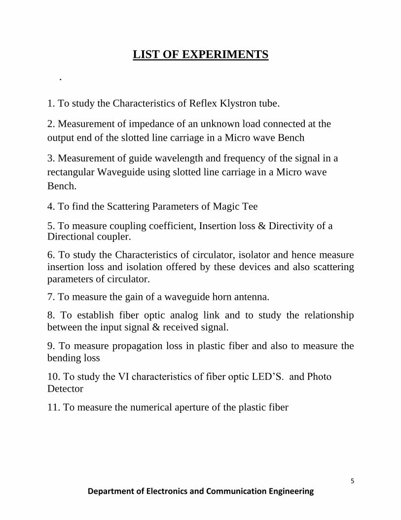
LIST OF EXPERIMENTS
.
1. To study the Characteristics of Reflex Klystron tube.
2. Measurement of impedance of an unknown load connected at the
output end of the slotted line carriage in a Micro wave Bench
3. Measurement of guide wavelength and frequency of the signal in a
rectangular Waveguide using slotted line carriage in a Micro wave
Bench.
4. To find the Scattering Parameters of Magic Tee
5. To measure coupling coefficient, Insertion loss & Directivity of a Directional coupler.
6. To study the Characteristics of circulator, isolator and hence measure
insertion loss and isolation offered by these devices and also scattering
parameters of circulator.
7. To measure the gain of a waveguide horn antenna.
8. To establish fiber optic analog link and to study the relationship
between the input signal & received signal.
9. To measure propagation loss in plastic fiber and also to measure the
bending loss
10. To study the VI characteristics of fiber optic LED’S. and Photo
Detector
11. To measure the numerical aperture of the plastic fiber

6
Department of Electronics and Communication Engineering
INDEX
S.NO. NAME OF EXPERIMENT DATE OF
EVALUATION GRADE
7
Department of Electronics and Communication Engineering
Experiment No.-1
Objective: To study the Characteristics of Reflex Klystron tube
Equipments required:
Klystron tube, Klystron power supply, Klystron mount, Isolator, Frequency Meter, Variable
Attenuator, Detector mount, Wave guide stand, Cooling fan, VSWR meter, Cables and
accessories.
Theory:
The Reflex Klystron makes the use of velocity modulation to transform a continuous electron
beam into microwave power. Electrons emitted from the cathode are accelerated & passed
through the positive resonator towards negative reflector, which retards and finally reflects the
electrons and the electrons turn back through the resonator. Suppose an RF-field exists between
the resonators, the electrons traveling for-ward will be accelerated or retarded, as the voltage at
the resonator changes in amplitude. The accelerated electrons leave the resonator at an increased
velocity and the retarded electrons leave at the reduced velocity. The electrons leaving the
resonator will need different time to return, due to change in velocities. As a result, returning
electrons group together in bunches, as the electron bunches pass through resonator, they interact
with voltage at resonator grids. If the bunches pass the grid at such a time that the electrons are
slowed down by the voltage then energy will be delivered to the resonator; and Klystron will
oscillate.
Procedure:
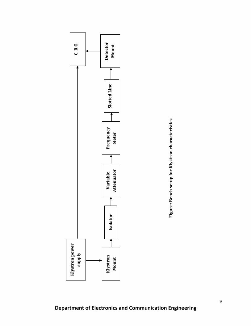
(1) Set up the components and equipment as shown in fig.
(2) Keep position of variable attenuator at minimum position.
(3) Keep beam voltage knob fully anti-clock wise and repeller voltage to fully clockwise.
(4) Switch on the Klystron power supply and oscilloscope.
(5) Switch on beam voltage switch (HT) and set beam voltage to 300v by beam voltage
control knob,
(6) Keep amplifier knob of FM modulator to maximum position and rotate the reflector
voltage anticlockwise to get modes.
8
Department of Electronics and Communication Engineering
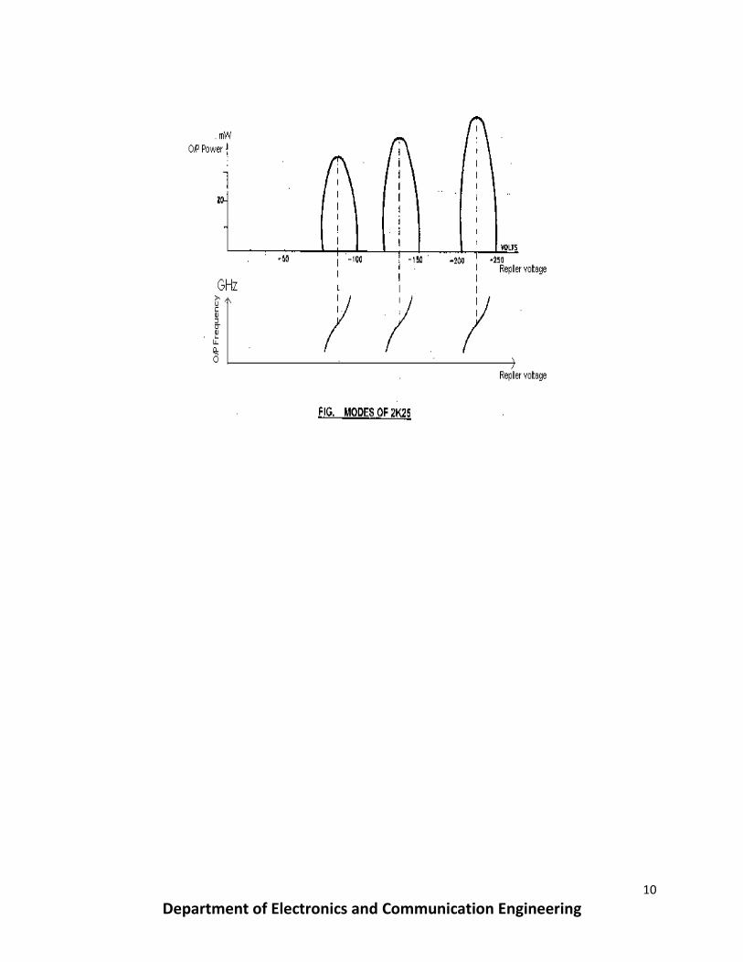
(7) By changing the repeller voltage and amplitude of FM modulation, any mode of klystron
tube can be seen on CRO.
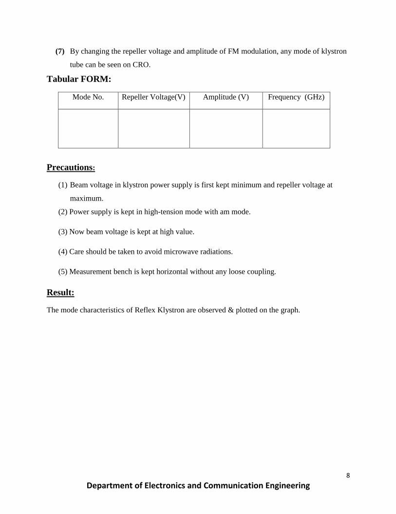
Tabular FORM:
Mode No. Repeller Voltage(V) Amplitude (V) Frequency (GHz)
Precautions:
(1) Beam voltage in klystron power supply is first kept minimum and repeller voltage at
maximum.
(2) Power supply is kept in high-tension mode with am mode.
(3) Now beam voltage is kept at high value.
(4) Care should be taken to avoid microwave radiations.
(5) Measurement bench is kept horizontal without any loose coupling.
Result:
The mode characteristics of Reflex Klystron are observed & plotted on the graph.
9
Department of Electronics and Communication Engineering
Kly
stro
n
Mo
un
t Is
ola
tor
Va
ria
ble
Att
en
ua
tor
Fre
qu
en
cy
Me
ter
Slo
tte
d L
ine
C R
O
De
tect
or
Mo
un
t
Kly
stro
n p
ow
er
sup
ply
Fig
ure
: Be
nch
se
tup
fo
r K
lyst
ron
ch
ara
cte
rist
ics
10
Department of Electronics and Communication Engineering
11
Department of Electronics and Communication Engineering
Experiment No.-2
Objective:
Measurement of impedance of an unknown load connected at the output end of the slotted line
carriage in a Micro wave Bench
Equipment required:
Klystron Power Supply, Reflex Klystron Tube with Klystron Mount, Isolator, Frequency Meter,
Variable Attenuator, Slotted Line, Tunable Probe, Detector Mount, Wave Guide Stands, VSWR
Meter, Oscilloscope, Movable Short /Termination or any unknown load.
Theory:
The impedance at any point on a transmission line can be written in the form R+jx. For comparison SWR
can be calculated
1
1
RS
R
Where Reflection coefficient (R ) 0
0
Z Z
Z Z
Zo = Characteristics impedance of wIg at operating frequency.
Z is the load impedance. The measurement is performed in following way.
The unknown device is connected to the slotted line and the position of one minima’s is determined. The
unknown device is replaced by movable short to the slotted. Line. Two successive minima positions are
noted. The twice of the difference between minima position will be guide wavelength. One of the minima
is used as reference for Impedance measurement. Find the difference of reference minima and minima
position obtained from unknown load. Let it be 'd'. Take a smith chart, taking '1' as center, draw a circle of
radius equal to so. Mark a point on circumference of smith chart towards load side at a distance equal to
dli.g. Join the center with this point. Find the point where it cut the drawn circle. The co-ordinates 'of this
point will show the normalized impedance of load.
12
Department of Electronics and Communication Engineering
Procedure:
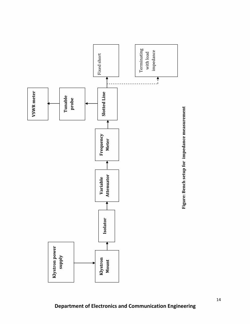
1. Set up the equipment’s as shown in the figure.
2. Set the variable attenuator at minimum position.
3. Keep the control knobs of VSWR Meter as below
a. Range - 50db positions
b. Input Switch - Crystal Low Impedance
c. Meter Switch - Normal position
d. Gain (Coarse-Fine) - Mid position
4. Keep the Control. Knobs of Klystron power supply as below
a. Beam voltage switch - OFF
b. Mod switch - AM
c. Beam Voltage knob - Fully anticlockwise
d. Reflector Voltage - Fully clockwise
e. AM - Amplitude - Around fully clockwise
f. AM - Frequency knob - Around Mid position.
5. Switch 'ON' the Klystron power supply, VSWR Meter and cooling fan.
6. Switch 'ON' the Beam Voltage Switch position and set beam voltage at 300 V with help of beam
voltage knob.
7. Adjust the reflector voltage knob to get some deflection in VSWR Meter.
8. Maximize the deflection with AM amplitude and frequency control knob of power supply.
9. Tune the plunger of Klystron Mount for Maximum deflection.
10. Tune the reflector voltage knob for maximum deflection.
11. Tune the probe for maximum deflection in VSWR meter.
12. Tune the frequency meter knob to get a 'dip' on the VSWR meter and note down the frequency
directly from frequency meter.
13. Load end terminate with the device under test (DUT). Find VSWR of DUT using direct method
or double minima method accordingly.
14. Note down the SWR S. also note down the minima position, let it be d.
15. Remove DUT and place moveable short at slotted line. The plunger of short should be at zero.
(i.e. moveable short is used as short).
16. Note the position of two successive minima position. Let it be as d1 and d2 . Hence
λg = 2(d1~ d2)
17. calculate d/ λg find out normalized impedance.

13
Department of Electronics and Communication Engineering
Observations:
Frequency
of Excited
Wave
Load
VSWR
Position of minimum Shift in
minima
</4=(d)
Direction of shift
towards
load/generator
Load Short
dl1 d1
dl2 d2
Calculations:
(A). Using formula:
The impedance can be calculated by using the following formula
Zin = Zo { [1-j S tan (2d/g)] / [S-j tan (2d/g) ] }
Where Zo = / { 1- (2o /
2c )
(+d) is for shift in minima towards load.
(-) is for shift in minima towards generator.
Precautions:
1. Keep the cooling fan towards the reflex Klystron.
2. Do not look into the transmitting Horn.
3. Do not apply ever repellar voltages as zero volts.
Result:
The unknown load impendence is calculated using formula and is verified.
14
Department of Electronics and Communication Engineering
Fig
ure
: Be
nch
se
tup
fo
r i
mp
ed
an
ce m
ea
sure
me
nt
Kly
stro
n
Mo
un
t Is
ola
tor
Va
ria
ble
Att
en
ua
tor
Fre
qu
en
cy
Me
ter
Slo
tte
d L
ine
F
ixed
sh
ort
Kly
stro
n p
ow
er
sup
ply
T
un
ab
le
pro
be
VS
WR
me
ter
Ter
min
atin
g
wit
h lo
ad
imp
edan
ce
15
Department of Electronics and Communication Engineering
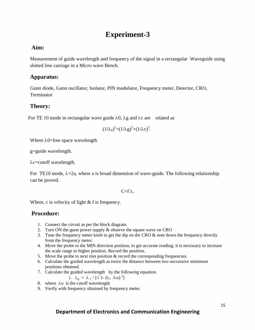
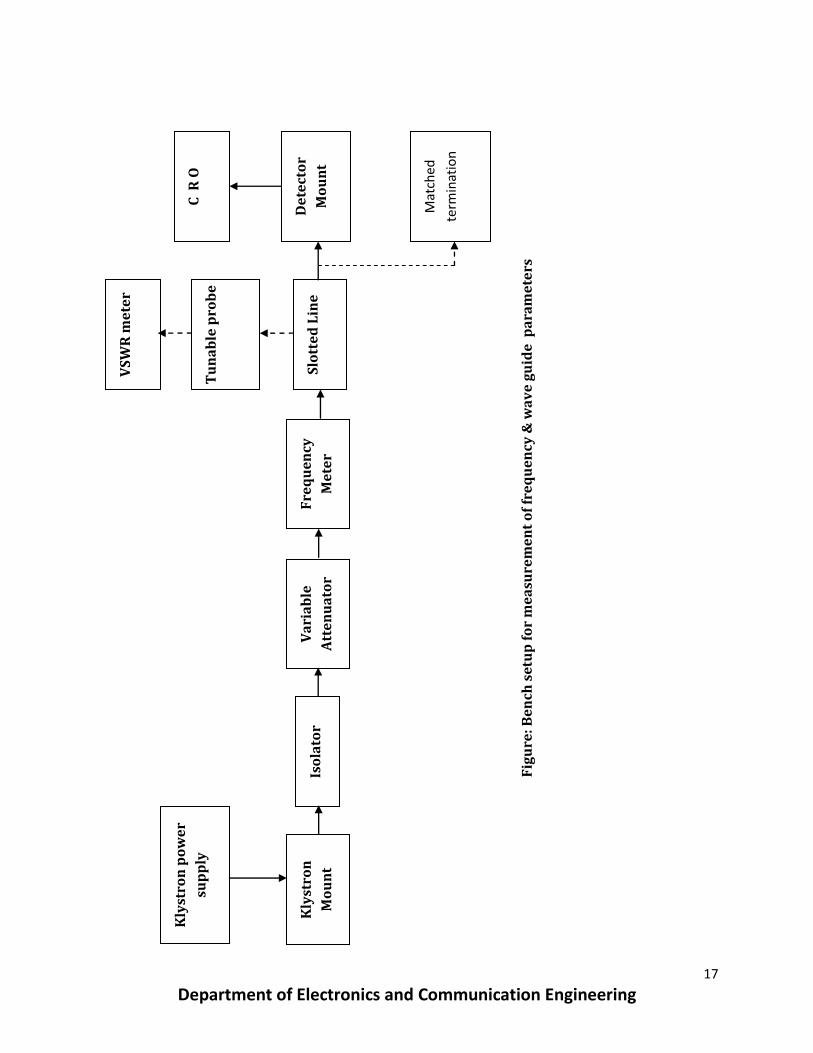
Experiment-3
Aim:
Measurement of guide wavelength and frequency of the signal in a rectangular Waveguide using
slotted line carriage in a Micro wave Bench.
Apparatus:
Gunn diode, Gunn oscillator, Isolator, PIN modulator, Frequency meter, Detector, CRO,
Terminator
Theory:
For TE 10 mode in rectangular wave guide 0, g and c are related as
(1/0)2=(1/g)
2+(1/c)
2.
Where 0=free space wavelength
g=guide wavelength.
c=cutoff wavelength.
For TE10 mode, =2a, where a is broad dimension of wave-guide. The following relationship
can be proved.
C=f .
Where, c is velocity of light & f is frequency.
Procedure:
1. Connect the circuit as per the block diagram.
2. Turn ON the gunn power supply & observe the square wave on CRO
3. Tune the frequency meter knob to get the dip on the CRO & note down the frequency directly
from the frequency meter.
4. Move the probe to the MIN direction position, to get accurate reading; it is necessary to increase
the scale range to higher position. Record the position.
5. Move the probe to next min position & record the corresponding frequencies.
6. Calculate the guided wavelength as twice the distance between two successive minimum
positions obtained.
7. Calculate the guided wavelength by the following equation.
i. g = f / [ 1- (f /o) 2]
8. where o is the cutoff wavelength
9. Verify with frequency obtained by frequency meter.

16
Department of Electronics and Communication Engineering
Calculations:
(1/0) = [(1/g)2+(1/c)
2]
and ‘f ‘is found from the above formula.
Precautions:
1. Care should be taken to avoid microwave radiation.
2. Loose coupling must be avoided.
3. Output signal is kept as high as possible.
4. Care should be taken while increasing distance on vernier scale.
Result:
Hence measured the frequency and waveguide parameters.
17
Department of Electronics and Communication Engineering
Fig
ure
: Be
nch
se
tup
fo
r m
ea
sure
me
nt
of
fre
qu
en
cy &
wa
ve
gu
ide
pa
ram
ete
rs
Kly
stro
n
Mo
un
t Is
ola
tor
Va
ria
ble
Att
en
ua
tor
Fre
qu
en
cy
Me
ter
Slo
tte
d L
ine
C R
O
De
tect
or
Mo
un
t
Kly
stro
n p
ow
er
sup
ply
Tu
na
ble
pro
be
Mat
ched
term
inat
ion
VS
WR
me
ter
18
Department of Electronics and Communication Engineering
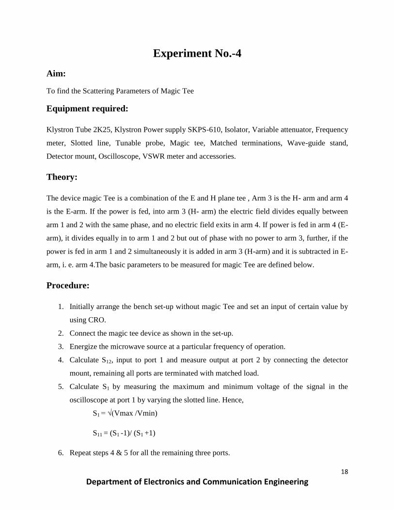
Experiment No.-4
Aim:
To find the Scattering Parameters of Magic Tee
Equipment required:
Klystron Tube 2K25, Klystron Power supply SKPS-610, Isolator, Variable attenuator, Frequency
meter, Slotted line, Tunable probe, Magic tee, Matched terminations, Wave-guide stand,
Detector mount, Oscilloscope, VSWR meter and accessories.
Theory:
The device magic Tee is a combination of the E and H plane tee , Arm 3 is the H- arm and arm 4
is the E-arm. If the power is fed, into arm 3 (H- arm) the electric field divides equally between
arm 1 and 2 with the same phase, and no electric field exits in arm 4. If power is fed in arm 4 (E-
arm), it divides equally in to arm 1 and 2 but out of phase with no power to arm 3, further, if the
power is fed in arm 1 and 2 simultaneously it is added in arm 3 (H-arm) and it is subtracted in E-
arm, i. e. arm 4.The basic parameters to be measured for magic Tee are defined below.
Procedure:
1. Initially arrange the bench set-up without magic Tee and set an input of certain value by
using CRO.
2. Connect the magic tee device as shown in the set-up.
3. Energize the microwave source at a particular frequency of operation.
4. Calculate S12, input to port 1 and measure output at port 2 by connecting the detector
mount, remaining all ports are terminated with matched load.
5. Calculate S1 by measuring the maximum and minimum voltage of the signal in the
oscilloscope at port 1 by varying the slotted line. Hence,
S1 = √(Vmax /Vmin)
S11 = (S1 -1)/ (S1 +1)
6. Repeat steps 4 & 5 for all the remaining three ports.
19
Department of Electronics and Communication Engineering
Observations:
S11 S12 S13 S14
S21 S22 S23 S24
S = S31 S32 S33 S34
S41 S42 S43 S44
Precautions:
1. Keep the cooling fan towards the reflex Klystron.
2. Do not look into the transmitting Horn.
3. Do not apply ever repellar voltages as zero volts.
Result:
The scattering matrix of magic tee is found.
20
Department of Electronics and Communication Engineering
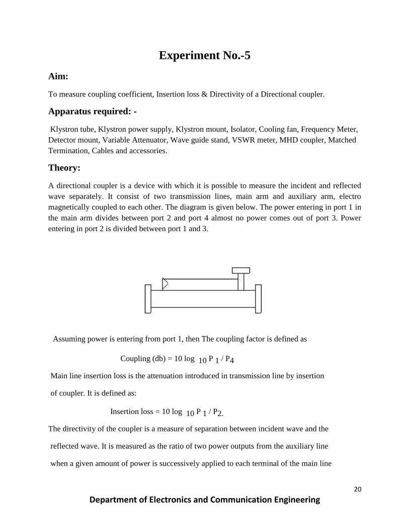
Experiment No.-5
Aim:
To measure coupling coefficient, Insertion loss & Directivity of a Directional coupler.
Apparatus required: -
Klystron tube, Klystron power supply, Klystron mount, Isolator, Cooling fan, Frequency Meter,
Detector mount, Variable Attenuator, Wave guide stand, VSWR meter, MHD coupler, Matched
Termination, Cables and accessories.
Theory:
A directional coupler is a device with which it is possible to measure the incident and reflected
wave separately. It consist of two transmission lines, main arm and auxiliary arm, electro
magnetically coupled to each other. The diagram is given below. The power entering in port 1 in
the main arm divides between port 2 and port 4 almost no power comes out of port 3. Power
entering in port 2 is divided between port 1 and 3.
Assuming power is entering from port 1, then The coupling factor is defined as
Coupling (db) = 10 log 10 P 1 / P4
Main line insertion loss is the attenuation introduced in transmission line by insertion
of coupler. It is defined as:
Insertion loss = 10 log 10 P 1 / P2.
The directivity of the coupler is a measure of separation between incident wave and the
reflected wave. It is measured as the ratio of two power outputs from the auxiliary line
when a given amount of power is successively applied to each terminal of the main line
21
Department of Electronics and Communication Engineering
with other port terminated by matched load. Hence Directivity is given by
D (db) = 10 log 10 P4f / P4r
Where P4f is the measured power at port 4 with equal amount of power is fed and P4r to
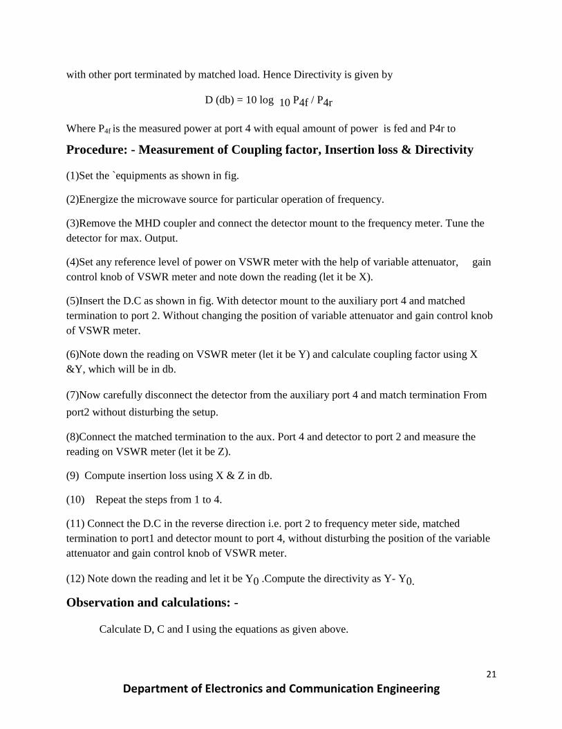
Procedure: - Measurement of Coupling factor, Insertion loss & Directivity
(1)Set the `equipments as shown in fig.
(2)Energize the microwave source for particular operation of frequency.
(3)Remove the MHD coupler and connect the detector mount to the frequency meter. Tune the
detector for max. Output.
(4)Set any reference level of power on VSWR meter with the help of variable attenuator, gain
control knob of VSWR meter and note down the reading (let it be X).
(5)Insert the D.C as shown in fig. With detector mount to the auxiliary port 4 and matched
termination to port 2. Without changing the position of variable attenuator and gain control knob
of VSWR meter.
(6)Note down the reading on VSWR meter (let it be Y) and calculate coupling factor using X
&Y, which will be in db.
(7)Now carefully disconnect the detector from the auxiliary port 4 and match termination From
port2 without disturbing the setup.
(8)Connect the matched termination to the aux. Port 4 and detector to port 2 and measure the
reading on VSWR meter (let it be Z).
(9) Compute insertion loss using X & Z in db.
(10) Repeat the steps from 1 to 4.
(11) Connect the D.C in the reverse direction i.e. port 2 to frequency meter side, matched
termination to port1 and detector mount to port 4, without disturbing the position of the variable
attenuator and gain control knob of VSWR meter.
(12) Note down the reading and let it be Y0 .Compute the directivity as Y- Y0.
Observation and calculations: -
Calculate D, C and I using the equations as given above.

22
Department of Electronics and Communication Engineering
Result
The measured value for MHD coupler are
Coupling coefficient =
Insertion loss =
Directivity =
23
Department of Electronics and Communication Engineering
Kly
stro
n
Mo
un
t Is
ola
tor
Va
ria
ble
Att
en
ua
tor
Fre
qu
en
cy
Me
ter
Slo
tte
d L
ine
C R
O
De
tect
or
Mo
un
t
Kly
stro
n p
ow
er
sup
ply
Tu
na
ble
pro
be
Mat
ched
term
inat
ion
VS
WR
me
ter
24
Department of Electronics and Communication Engineering
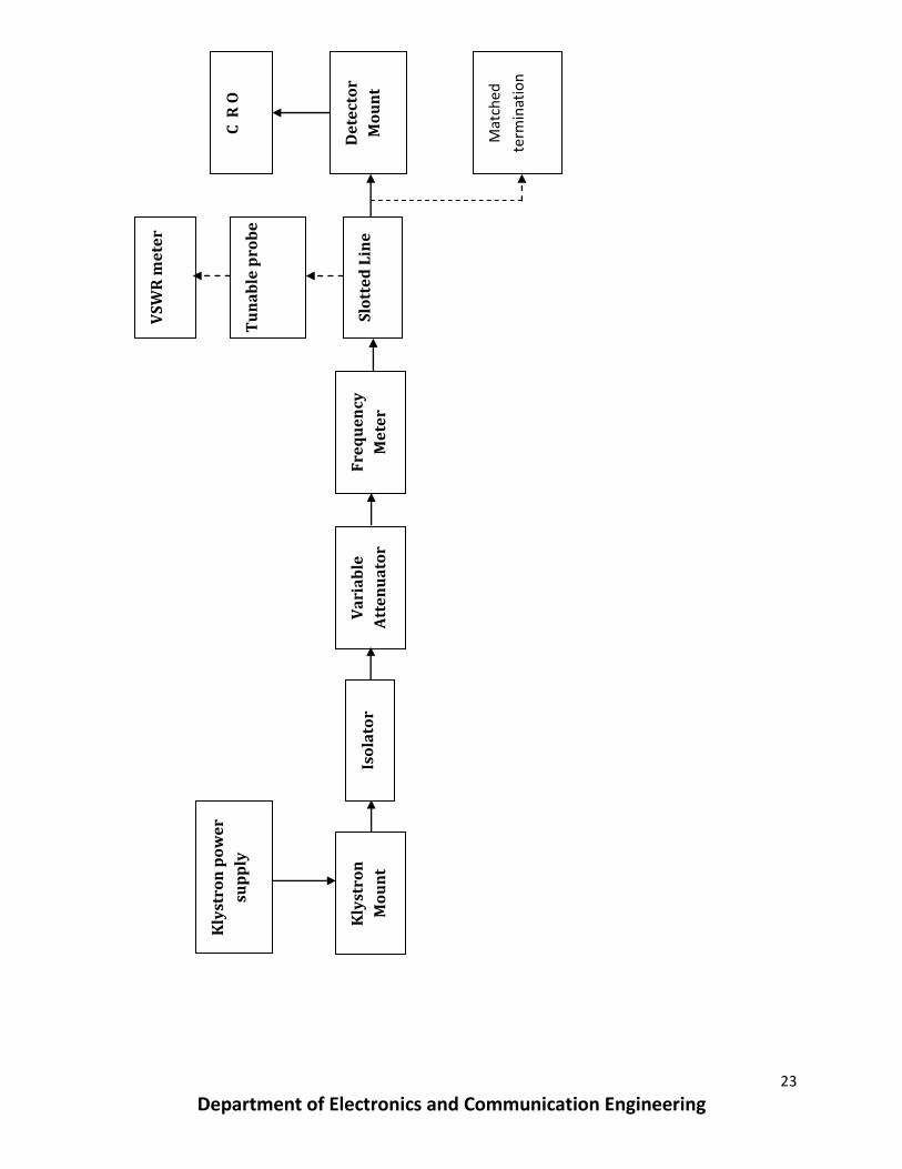
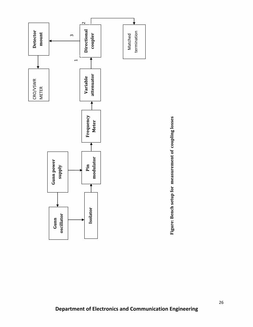
Experiment no.-6
Aim:
To study the Characteristics of circulator, isolator and hence measure insertion loss and isolation
offered by these devices and also scattering parameters of circulator.
Equipment required:
Klystron Power Supply, Reflex Klystron Tube with Klystron Mount, Isolator, Frequency Meter,
Variable Attenuator, Slotted Line, Tunable Probe, Detector Mount, Wave Guide Stands, VSWR
Meter, Oscilloscope, Movable Short /Termination, circulator, isolator.
Theory:
Ferrites are non-metallic materials with magnetic properties. Ferrites have one more peculiar
property, which is useful at microwave frequencies, i.e, and the non-reciprocal property. When
two circular polarized waves one rotating clockwise and other anti-clockwise are made to
propagate through ferrite, the material reacts differently to the two rotating fields, thereby
presenting different effective permeability’s to both the waves. Isolator and circulator are two
microwave devices that make use of Faraday rotation principle.
Circulator
Circulator is multi-port device such that wave incident on nth port is coupled to (n+1)th port
only. That is if power is incident in port 1, port 2 is coupled but not port 3.
Isolator
An isolator is a two - ports device that transfers energy from input to output with little
attenuation and from output to input with very high attenuation. This is generally used
between the source and rest of the setup to avoid over loading of the source due to reflected
power
Insertion Loss
25
Department of Electronics and Communication Engineering
Insertion Loss is the ratio of power supplied by a source to the input arm, to the power detected
by the detector in the coupled arm with all ports matched termination.
Isolation
Isolation is the ratio of power fed in arm 1 by a matched generator to the power detected in port 3
by detector with port 2 terminated in matched loads.
Procedure:
Measurement of Insertion loss and Isolation
1. Set up the components and equipment’s as shown in fig. without the ferrite device i.e.,
directly connect detector with VSWR meter in order to measure input.
2. Keep the control knobs of VSWR Meter as below
a. Range - 50db positions
b. Input Switch - Crystal Low Impedance
c. Meter Switch - Normal position
d. Gain (Coarse-Fine) - Mid position
3. Keep the Control. Knobs of Klystron power supply as below
a. Beam voltage switch - OFF
b. Mod switch - AM
c. Beam Voltage knob - Fully anticlockwise
d. Reflector Voltage - Fully clockwise
e. AM - Amplitude - Around fully clockwise
f. AM - Frequency knob - Around Mid position.
4. Energize the microwave source for particular frequency of operation.
5. Set some reference reading in VSWR meter by adjusting the variable attenuator. Note
this attenuator setting as (A1) dB.
26
Department of Electronics and Communication Engineering
Gu
nn
osc
illa
tor
Iso
lato
r P
in
mo
du
lato
r
Fre
qu
en
cy
Me
ter
Va
ria
ble
att
en
ua
tor
De
tect
or
mo
un
t
Dir
ect
ion
al
cou
ple
r
Gu
nn
po
we
r
sup
ply
1
2
3
Mat
ched
term
inat
ion
CR
O/V
SWR
MET
ER
Fig
ure
: Be
nch
se
tup
fo
r m
ea
sure
me
nt
of
co
up
lin
g l
oss
es
27
Department of Electronics and Communication Engineering
Experiment No.-7
Aim :
To measure the gain of a waveguide horn antenna.
Apparatus required :
Microwave source, Frequency meter, Isolator, Variable attenuator, Detector mount, Two horn
antenna, Turn table, VSWR meter and Accessories.
Theory:
If a transmission line propagating energy is left open at one end, there will be radiation from this
end. In case of a rectangular waveguide this antenna presents a mismatch of about 2 : 1 and it
radiates in many directions. The match will improve if the open waveguide is a horn shape. The
radiation pattern of an antenna is a diagram of field strength or more often the power intensity as
a function of the aspect angle at a constant distance from the radiating antenna. The power
intensity at the maximum of the main lobe compared to the power intensity achieved from an
imaginary Omni directional antenna (radiating equally in all direction) with the same power fed
to the antenna is defined as in gain of the antenna.
3 db Beam Width
The angle between the two points on a main lobe where the power intensity is half the maximum
power intensity. When measuring an antenna pattern, it is normally most interesting to plot the
pattern far from the antenna.
Far field pattern is achieved at a minimum distance of 2D (for rectangular Horn Antenna)
0
where D is size of the broad wall of horn aperture in free space wave length.
It is also very important to avoid disturbing reflection. Antenna measurement are normally made
at outdoor rangers or in so called anechoic chambers made of absorbing materials.
Antenna measurements are mostly made with unknown antenna as receiver. There are several
methods to measure the gain of antenna. One method is to compare the unknown antenna with a
standard gain antenna with known gain. An another method is to use two identical antennas, as
transmitter and other as receiver from following formula the gain can be calculated.
Pr = P t 0 G 1G2
(4 S)
28
Department of Electronics and Communication Engineering
Where Pt = Transmitted Power ,
Pr = Received Power,
G1, G2 = Gain of transmitting & receiving antenna
t 0 = free space wavelength
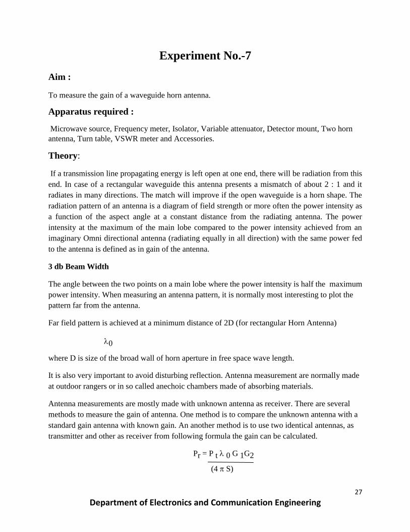
Block diagram:
Procedure: -
GAIN MEASUREMENT
1. Set up the equipments as shown in Fig. Both horns should be in line.
2. Keep the range db switch of VSWR meter at 50 db position with gain control full.
3. Energize the Gunn Oscillator for maximum output at desired frequency with modulating
amplitude and frequency of Gunn Power Supply and by tuning of detector.
4. Obtain full scale deflection in VSWR meter with variable attenuator.
5. Replace the transmitting horn by detector mount and change the appropriate range db position
to get the deflection on Scale (do not touch the gain control knob). Note and record the range db
position and deflection of VSWR meter.
6. Calculate the difference in db between the power measured in step 4 and 5.

29
Department of Electronics and Communication Engineering
7. Convert G into db in above example
G db =- 10 log 318 =- 15.02 db
8. The same set up can be used for other frequency of operation.
Precautions:-
1. Use fan to keep the Klystron temperature low.
2. Ensure tight connections of the apparatus
3. Avoid cross connections of the threads.
4. Use stabilized power supply.
30
Department of Electronics and Communication Engineering
Experiment No.-8
Aim:
To establish fiber optic analog link and to study the relationship between the input signal &
received signal.
Equipment required
Link-A kit, 1 Meter Fiber cable, 20 MHz Dual Channel Oscilloscope, Power supply
THEORY
Fiber Optic Links can be used for transmission of digital as well as analog signals. Basically a
fiber optic link contains three main elements, a transmitter, an optical fiber and a receiver. The
transmitter module takes the input signal in electrical form and then transforms it into optical
(light) energy containing the same information. The optical fiber is the medium, which carries
this energy to the receiver. At the receiver, light is converted back into electrical form with the
same pattern as originally fed to the transmitter.
TRANSMITTER
Fiber optic transmitters are typically composed of a buffer, driver and optical source. The buffer
electronics provides both an electrical connection and isolation between the transmitter and the
electrical system supplying the data. The driver electronics provides electrical power to the
optical source in a fashion that duplicates the pattern of data being fed to the transmitter. Finally
the optical source (LED) converts the electrical current to light energy with the same pattern. The
LED SFH756V supplied with the kit operates inside the visible light spectrum. Its optical output
is centered at near visible wavelength of 660 nm. The emission spectrum is broad, so a dark red
glow can usually be seen when the LED is on. The LED SFH450V supplied with the kit operates
outside the visible light spectrum. Its optical output is centered at near infrared wavelength of
950 nm.
RECEIVER
The function of the receiver is to convert the optical energy into electrical form, which is then
conditioned to reproduce the transmitted electrical signal in its original form. The detector

31
Department of Electronics and Communication Engineering
SFH250V used in the kit has a diode type output. The parameters usually considered in the case
of detector are it's responsivity at peak wavelength and response time. SFH250V has
responsivity of about 4 μA per 10 μW of incident optical energy at 950 nm and it has rise and
fall time of 0.01μsec. PIN photodiode is normally reverse biased. When optical signal falls on
the diode, reverse current start to flow, thus diode acts as closed switch and in the absence of
light intensity; it acts as an open switch. Since PIN diode usually has low responsivity, a trans
impedance amplifier is used to convert this reverse current into voltage. This voltage is then
amplified with the help of another amplifier circuit. This voltage is the duplication of the
transmitted electrical signal.
Procedure
1. Slightly unscrew the cap of LED SFH 756V TX1 (660 nm) from kit. Do not remove the
cap from the connector. Once the cap is loosened, insert the fiber into the cap and assure
that the fiber is properly fixed. Now tight the cap by screwing it back. Keep INTENSITY
pot P3 at minimum position i.e. fully anticlockwise.
2. Make the connections and jumper settings as shown in Fig. Connect the power supply
cables with proper polarity to kit. While connecting this, ensure that the power supply is
OFF.
3. Switch on the Power supply.
4. Select the frequency range of Function Generator with the help of Range Selection
Switch SW1, frequency can be varied with pot P2. adjust the voltage LEVEL of the sine
wave with pot P1 as per following setting
FREQUENCY: 1 KHz, LEVEL: 2V p-p
5. Connect SINE post of the Function Generator section to IN post of Analog Buffer
Section.
6. Connect OUT post of the Analog Buffer Section to TX IN post of TRANSMITTER.
7. Connect the other end of the fiber to detector SFH 250V (RX 1) in kit very carefully.
8. Check the output signal of the Analog Buffer at its OUT post in Kit. It should be same as
that of the applied input signal.
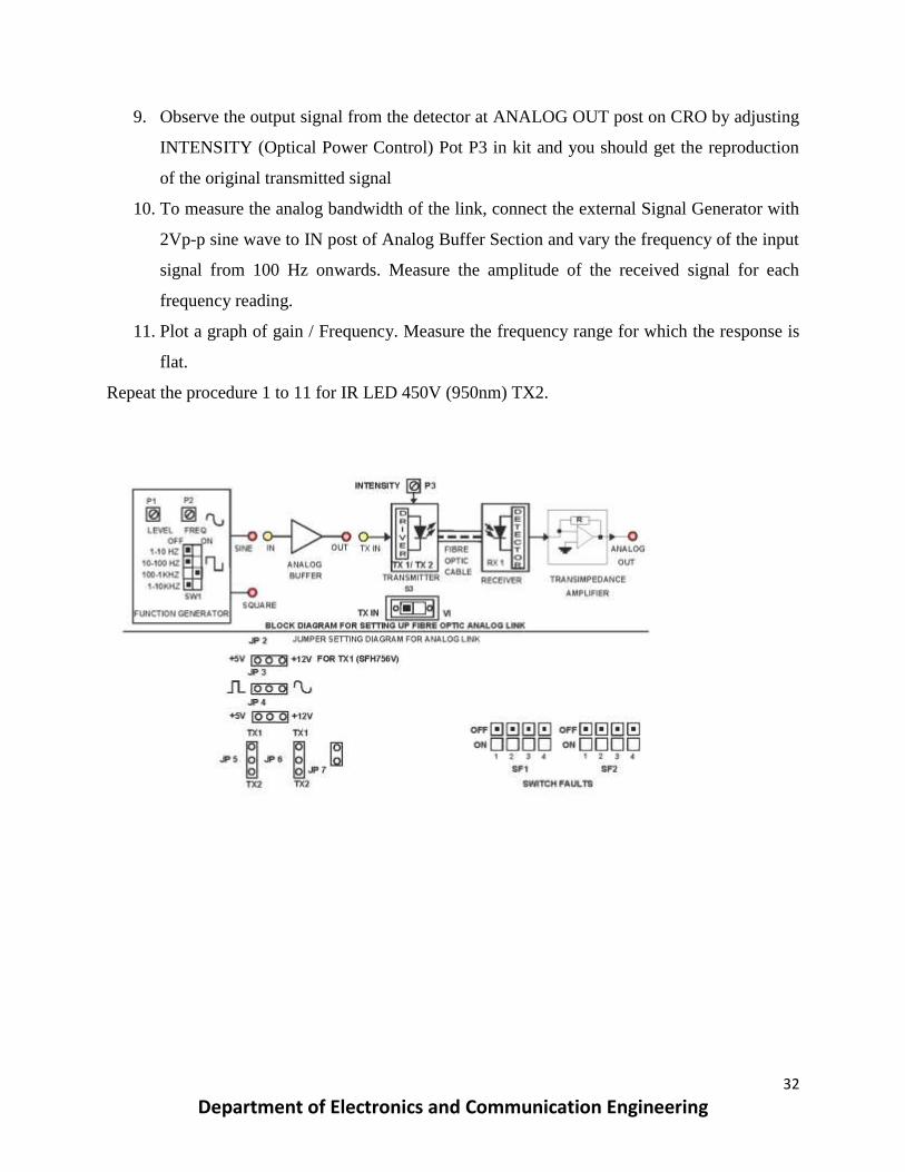
32
Department of Electronics and Communication Engineering
9. Observe the output signal from the detector at ANALOG OUT post on CRO by adjusting
INTENSITY (Optical Power Control) Pot P3 in kit and you should get the reproduction
of the original transmitted signal
10. To measure the analog bandwidth of the link, connect the external Signal Generator with
2Vp-p sine wave to IN post of Analog Buffer Section and vary the frequency of the input
signal from 100 Hz onwards. Measure the amplitude of the received signal for each
frequency reading.
11. Plot a graph of gain / Frequency. Measure the frequency range for which the response is
flat.
Repeat the procedure 1 to 11 for IR LED 450V (950nm) TX2.
33
Department of Electronics and Communication Engineering
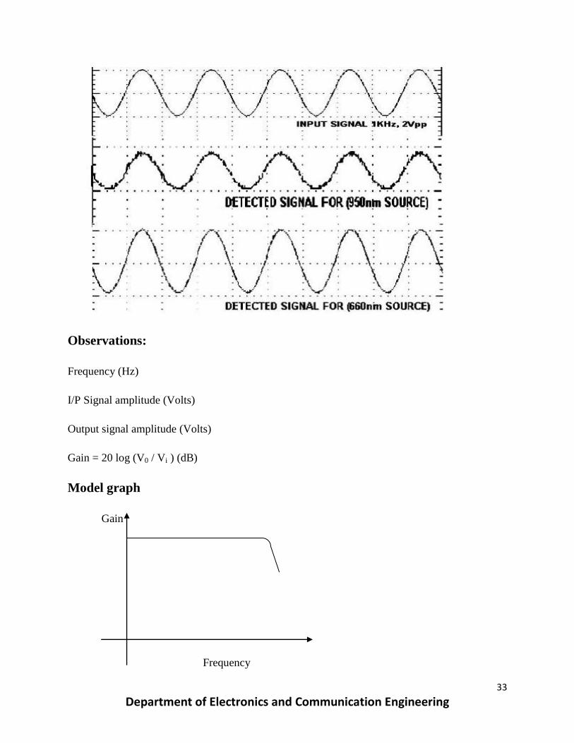
Observations:
Frequency (Hz)
I/P Signal amplitude (Volts)
Output signal amplitude (Volts)
Gain = 20 log (V0 / Vi ) (dB)
Model graph
Gain
Frequency
34
Department of Electronics and Communication Engineering
Precautions:
It is very important that the optical sources be properly aligned with the cable and the distance
from the launched point and the cable be properly selected to ensure that the maximum amount
of optical power is transferred to the cable.
Result:
On optical fiber link is established. The frequency response is observed. A graph is drawn
between gains in (dB) Vs frequency in Hz.
35
Department of Electronics and Communication Engineering
Experiment No.-9
Aim:
To measure propagation loss in plastic fiber and also to measure the bending loss
Equipment required:
Link-A kit, 20 MHz Dual Trace Oscilloscope, 1 & 3 Meter Fiber cable, Power supply.
Theory:
Optical fibers are available in different variety of materials. These materials are usually selected
by taking into account their absorption characteristics for different wavelengths of light. In case
of optical fiber, since the signal is transmitted in the form of light, which is completely different
in nature as that of electrons, one has to consider the interaction of matter with the radiation to
study the losses in fiber. Losses are introduced in fiber due to various reasons. As light
propagates from one end of fiber to another end, part of it is absorbed in the material exhibiting
absorption loss. Also part of the light is reflected back or in some other directions from the
impurity particles present in the material contributing to the loss of the signal at the other end of
the fiber. In general terms it is known as propagation loss. Plastic fibers have higher loss of the
order of 180 dB/Km. whenever the condition for angle of incidence of the incident light is
violated the losses are introduced due to refraction of light. This occurs when fiber is subjected
to bending. Lower the radius of curvature more is the loss. Another loss are due to the coupling
of fiber at LED and photo detector ends.
Procedure:
1. Slightly unscrew the cap of LED SFH 756V TX1 (660 nm) from kit. Do not remove the
cap from the connector. Once the cap is loosened, insert the fiber into the cap and assure
that the fiber is properly fixed. Now tight the cap by screwing it back. Keep INTENSITY
pot P3 at minimum position i.e. fully anticlockwise.
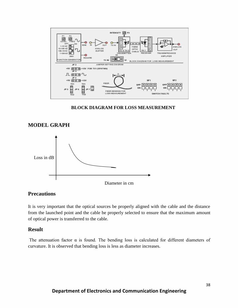
2. Make the connections and Jumper settings as shown in block diagram Connect the power
supply cables with proper polarity to kit. While connecting this, ensure that the power
supply is OFF.
36
Department of Electronics and Communication Engineering
3. Set the sine wave with 1 KHz, 2V p-p amplitude and connect it to IN post of analog
buffer.
4. Connect the other end of the fiber to detector SFH 250V (RX 1) in kit very carefully
Keep all the switch faults in OFF position.
5. Switch on the power supply.
6. Observe the output signal from the detector at ANALOG OUT post on CRO by adjusting
INTENSITY (Optical Power Control) Pot P3 in kit and you should get the reproduction
of the original transmitted signal. Mark this amplitude level as V1.
7. Now replace 1-meter fiber by 3-meter fiber without disturbing any of the previous
settings. Measure the amplitude level at the receiver side again. You will notice that it is
less than the previous one. Mark this as V2.
8. If alpha is the attenuation of the fiber then we have, P1/P2=V1/V2=e [-alpha (L1+L2)]
where alpha = nepers / meter L1 = fiber length for V1 L2 = fiber length for V2 This alpha
is for the wavelength of 950 nm. To get the alpha for 660 nm wavelengths proceed as
follows.
9. Repeat the above steps and replacing SFH 450V(950nm) by SFH 756V(660nm).
10. Make the Jumper settings as shown in the fig.
11. Compare the values of alpha and find out the wavelength, which has less attenuation in
the fiber.
Measurement of bending losses
1. Repeat all the steps from 1 to 11 as above.
2. Bend the fiber in a loop as shown in block diagram Measure the amplitude of the
received signal.
3. Keep reducing the diameter to about 2 cm & take corresponding output voltage readings.
(Do not reduce loop diameter less than 2 cm.)
4. Plot a graph of the received signal amplitude versus the loop diameter.
37
Department of Electronics and Communication Engineering
Calculations
For 1 mt cable
Input voltage (V1) = 1 Volt
Output voltage(V2) =
Frequency = 1KHz
For 3mt cable
Input voltage (V1) = 1 Volt
Output voltage(V2) =
Frequency = 1KHz
Attenuation loss
V1 / V2 = exp [- (l1 +l2) ] l1 = 1 mt ; l2 = 3mt ; = nepers / mt
Observations
Input voltage (V1) = 1 Volt
S.No Diameter
(cm)
Out put Voltage
(volts)
Loss in dB = -20 log10
( V0 / Vi )
38
Department of Electronics and Communication Engineering
BLOCK DIAGRAM FOR LOSS MEASUREMENT
MODEL GRAPH
Loss in dB
Diameter in cm
Precautions
It is very important that the optical sources be properly aligned with the cable and the distance
from the launched point and the cable be properly selected to ensure that the maximum amount
of optical power is transferred to the cable.
Result
The attenuation factor α is found. The bending loss is calculated for different diameters of
curvature. It is observed that bending loss is less as diameter increases.
39
Department of Electronics and Communication Engineering
Experiment No.10
Aim:
To study the VI characteristics of fiber optic LED’S. and Photo Detector
Equipment required
Link-A kit, 20 MHz Dual Trace Oscilloscope, 1 & 3 Meter Fiber cable, Power supply,
Voltmeter, Current meter, Jumper Connecting Wires-4.
Theory
In optical fiber communication system, electrical signal is first converted into optical signal with
the help of E/O conversion device as LED. After this optical signal is transmitted through optical
fiber, it is retrieved in its original electrical form with the help O/E conversion device as photo
detector.
Different technologies employed in chip fabrication lead to significant variation in parameters
for the various emitter diodes. All the emitters distinguish themselves in offering high output
power coupled into the plastic fiber. Data sheets for LEDs usually specify electrical and optical
characteristics, out of which are important peak wavelength of emission, conversion efficiency
(usually specified in terms of power launched in optical fiber for specified forward current),
optical rise and fall times which put the limitation on operating frequency, maximum forward
current through LED and typical forward voltage across LED.
Photo detectors usually come in variety of forms like photoconductive, photovoltaic, transistor
type output and diode type output. Here also characteristics to be taken into account are response
time of the detector, which puts the imitation on the operating frequency, wavelength sensitivity
and responsivity.
Procedure
(A) Characteristics of Fiber Optic LED
1. Make the jumper and switch settings as shown in the jumper diagram. Keep pot P4 in
fully clockwise position.
2. Connect the ammeter with the jumper connecting wires (provided along with the kit) in
jumpers JP3 as shown in the diagram.
40
Department of Electronics and Communication Engineering
3. Connect the voltmeter with the jumper wires to JP5 and JP2 at positions as shown in the
diagram.
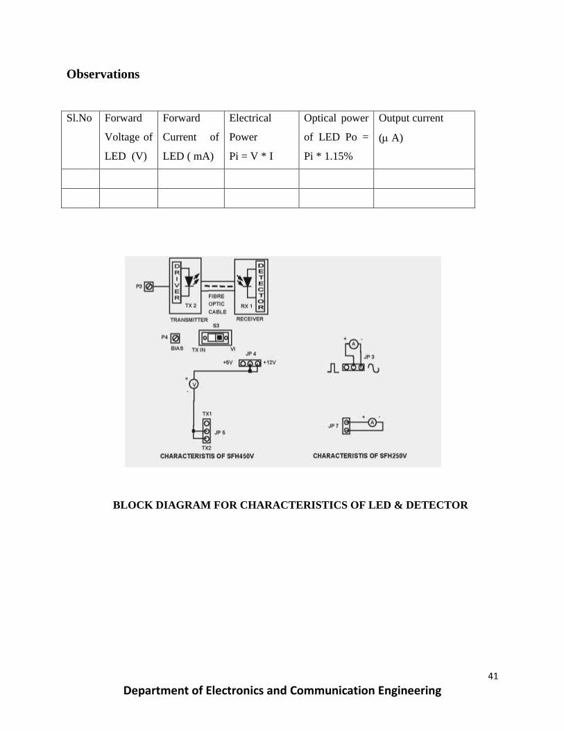
4. Switch on the power supply. Keep the potentiometer P3 in its minimum position (fully
anticlockwise position), P4 is used to control biasing voltage of the LED. To get the VI
characteristics of LED, rotate P3 slowly and measure forward current and corresponding
forward voltage of the LED, Take number of such readings for forward voltage, forward
current & optical power. Keep SW towards VI position.
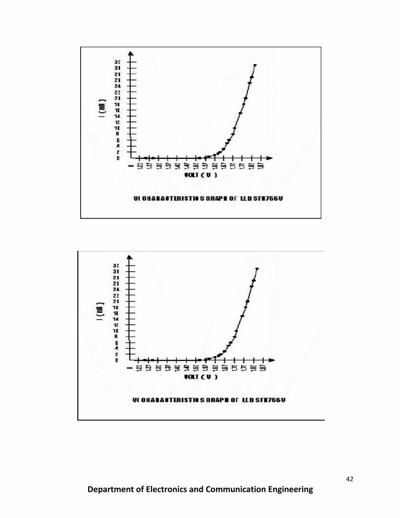
5. For each reading taken above, find out the power, which is product of I and V. This is the
electrical power supplied to the LED. Data sheets for the LED specifies optical power
coupled into plastic fiber when forward current was 10 micro A as 200microW. This
means that the electrical power at 10mA current is converted into 200 micro W of optical
energy. Hence the efficiency of the LED comes out to be approx. 1.15%.
6. With this efficiency assumed, find out optical power coupled into plastic optical fiber for
each of the reading in step 4. Plot the graph of forward current v/s output optical power of
the LED.
7. Repeat the above procedure by using SFH 450V (950 nm) LED.
(B) Characteristics of detector
1. Make the jumper and switch settings as shown in the jumper diagram. Keep pot P4 in
fully clockwise position.
2. Connect the ammeter with the jumper connecting wires (provided along with the kit) in
jumpers JP7 as shown in the diagram.
3. Connect 1Meter Fiber between TX1 & RX1.
4. Measure the current flowing through Detector (RX1) SFH250V at corresponding optical
power output (Normally in u A) as per the table.
5. We can observe that as incident optical power on detector increases, current flowing
through the detector increases.
41
Department of Electronics and Communication Engineering
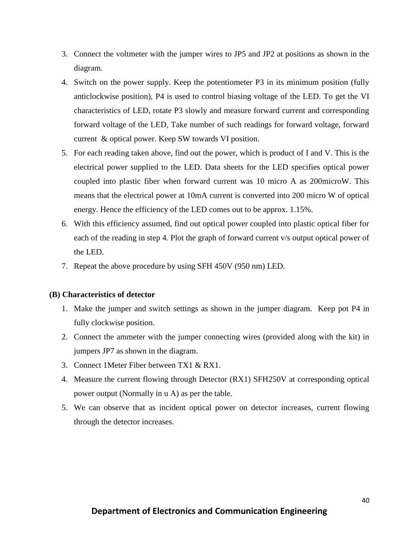
Observations
Sl.No Forward
Voltage of
LED (V)
Forward
Current of
LED ( mA)
Electrical
Power
Pi = V * I
Optical power
of LED Po =
Pi * 1.15%
Output current
( A)
BLOCK DIAGRAM FOR CHARACTERISTICS OF LED & DETECTOR
42
Department of Electronics and Communication Engineering
43
Department of Electronics and Communication Engineering
Precautions
It is very important that the optical sources be properly aligned with the cable and the distance
from the launched point and the cable be properly selected to ensure that the maximum amount
of optical power is transferred to the cable.
Result:
The characteristics of LED & DETECTOR are found.
44
Department of Electronics and Communication Engineering
Experiment No.-11
Aim:
To measure the numerical aperture of the plastic fiber
Equipment required
Link-A kit, 1 Meter Fiber cable, NA JIG, Steel Ruler, Power supply
Theory
Numerical aperture refers to the maximum angle at which the light incident on the fiber end is
totally internally reflected and is transmitted properly along the fiber. The cone formed by the
rotation of this angle along the axis of the fiber is the cone acceptance of the fiber. The light ray
should strike the fiber end within its cone of acceptance, else it is refracted out of the fiber core.
Considerations in na measurement
1. It is very important that the optical source should be properly aligned with the cable and
distance from the launched point and the cable is properly selected to ensure that the
maximum amount of optical power is transferred to the cable.
This experiment is best performed in a less illuminated room.
Procedure
1. Slightly unscrew the cap of LED SFH756V (660 nm). Do not remove the cap from the
connector. Once the cap is loosened, insert the fiber into the cap. Now tight the cap by
screwing it back. Keep Jumpers JP2 towards +5V position, JP3 towards sine position,
JP5 & JP6 towards TX1 position.
2. Connect the power supply cables with proper polarity to kit. While connecting this,
ensure that the power supply is OFF. Do not apply any TTL signal from Function
Generator. Make the connections as shown in block diagram.
3. Keep Pot P3 fully Clockwise Position and P4 fully anticlockwise position.
4. Switch on the power supply.
5. Insert the other end of the fiber into the numerical aperture measurement jig. Hold the
white sheet facing the fiber. Adjust the fiber such that its cut face is perpendicular to the
axis of the fiber.
45
Department of Electronics and Communication Engineering
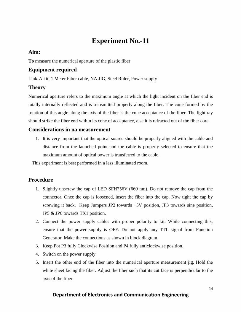
6. Keep the distance of about 10 mm between the fiber tip and the screen. Gently tighten the
screw and thus fix the fiber in the place.
7. Now adjust Pot P4 fully Clockwise Position and observe the illuminated circular patch of
light on the screen.
8. Measure exactly the distance d and also the vertical and horizontal diameters MR and PN
indicated in the block diagram.
9. Mean radius is calculated using the following formula. r = (MR + PN) / 4
10. Find the numerical aperture of the fiber using the formula. NA =
sinmax = r / √d2+ r
2
Where max is the maximum angle at which the light incident is properly transmitted
through the fiber
BLOCK DIAGRAM FOR NUMERICAL APERTURE SET UP
46
Department of Electronics and Communication Engineering
Observations
Sl.No Distance between source
and center of circular
patch AO = d cm
Vertical
Diameter
MR cm
Horizontal
diameter
PN cm
Calculations
Mean radius r = (MR+PN) /4
Numerical Aperture NA = sinmax = r / √d2+ r
2
Precautions
It is very important that the optical sources be properly aligned with the cable and the distance
from the launched point and the cable be properly selected to ensure that the maximum amount
of optical power is transferred to the cable.
Result
The Numerical Aperture of the optical fiber is found.