Keysight RF Microwave Lab Courseware – Preview Package Note: This is a preview lab sheet sample package which covering lab 1 to lab 7 This preview lab package only displays selected pages or sections from each lab

Welcome message from author
This document is posted to help you gain knowledge. Please leave a comment to let me know what you think about it! Share it to your friends and learn new things together.
Transcript
Keysight RF Microwave Lab Courseware – Preview Package Note: This is a preview lab sheet sample package
which covering lab 1 to lab 7 This preview lab package only displays
selected pages or sections from each lab
Keysight RF Microwave Circuit Design, Simulation and Measurement Courseware, 5G NR Band 2
Keysight RF Microwave Lab Courseware RF Microwave Circuit Design, Simulation and Measurement Courseware, 5G NR Band Lab 1: Transmission Lines
Lab Sheet
Keysight RF Microwave Circuit Design, Simulation and Measurement Courseware, 5G NR Band 3
Notices
Copyright Notice © Keysight Technologies 2019 No part of this manual may be reproduced in any form or by any means (including electronic storage and retrieval or translation into a foreign language) without prior agreement and written consent from Keysight Technologies as governed by United States and international copyright laws.
Trademarks Wi-Fi® is a registered trademark of Wi-Fi Alliance®.
Edition Edition 1, May 2019
Printed in: Printed in Malaysia
All rights reserved. License terms – see www.keysight.com/find/courseware
Published by: Keysight Technologies Bayan Lepas Free Industrial Zone, 11900 Penang, Malaysia
Technology Licenses The hardware and/or software described in this document are furnished under a license and may be used or copied only in accordance with the terms of such license.
Declaration of Conformity Declarations of Conformity for this product and for other Keysight products may be downloaded from the Web. Go to http://www.keysight.com/go/conformity. You can then search by product number to find the latest Declaration of Conformity.
U.S. Government Rights The Software is “commercial computer software,” as defined by Federal Acquisition Regulation (“FAR”) 2.101. Pursuant to FAR 12.212 and 27.405-3 and Department of Defense FAR Supplement (“DFARS”) 227.7202, the U.S. government acquires commercial computer software under the same terms by which the software is customarily provided to the public. Accordingly, Keysight provides the Software to U.S. government customers under its standard commercial license, which is embodied in its End User License Agreement (EULA), a copy of which can be found at http://www.keysight.com/find/sweula. The license set forth in the EULA represents the exclusive authority by which the U.S. gov-ernment may use, modify, distribute, or dis-close the Software. The EULA and the li-cense set forth therein, does not require or permit, among other things, that Keysight: (1) Furnish technical information related to commercial computer software or com-mercial computer software documentation that is not customarily provided to the public; or (2) Relinquish to, or otherwise provide, the government rights in excess of these rights customarily provided to the public to use, modify, reproduce, release, perform, display, or disclose commercial computer software or commercial computer software documentation. No additional government requirements beyond those set forth in the EULA shall apply, except to the extent that those terms, rights, or licenses are explicitly required from all providers of commercial computer software pursuant to the FAR and the DFARS and are set forth specifically in writing else- where in the EULA. Keysight shall be under no obligation to update, revise or otherwise modify the Software. With respect to any technical data as defined by FAR 2.101, pursuant to FAR 12.211 and 27.404.2 and DFARS 227.7102, the U.S. government acquires no greater than Limited Rights as defined in FAR 27.401 or DFAR 227.7103-5 (c), as applicable in any technical data.
Warranty THE MATERIAL CONTAINED IN THIS DOCUMENT IS PROVIDED “AS IS,” AND IS SUBJECT TO BEING CHANGED, WITHOUT NOTICE, IN FUTURE EDI-TIONS. FURTHER, TO THE MAXIMUM EXTENT PERMITTED BY APPLICABLE LAW, KEYSIGHT DISCLAIMS ALL WAR-RANTIES, EITHER EXPRESS OR IM-PLIED, WITH REGARD TO THIS MANU-AL AND ANY INFORMATION CON-TAINED HEREIN, INCLUD ING BUT NOT LIMITED TO THE IMPLIED WARRANTIES OF MERCHANTABILITY AND FITNESS FOR A PARTICULAR PURPOSE. KEYSIGHT SHALL NOT BE LIABLE FOR ERRORS OR FOR INCIDENTAL OR CONSEQUENTIAL DAMAGES IN CONNECTION WITH THE FURNISHING, USE, OR PERFORMANCE OF THIS DOCUMENT OR OF ANY INFORMATION CON- TAINED HEREIN. SHOULD KEYSIGHT AND THE USER HAVE A SEPARATE WRITTEN AGREEMENT WITH WAR-RANTY TERMS COVERING THE MATE-RIAL IN THIS DOCUMENT THAT CON-FLICT WITH THESE TERMS, THE WAR-RANTY TERMS IN THE SEPARATE AGREEMENT SHALL CONTROL.
Safety Information
CAUTION A CAUTION notice denotes a hazard. It calls attention to an operating procedure, practice, or the like that, if not correctly performed or adhered to, could result in damage to the product or loss of important data. Do not proceed beyond a CAUTION notice until the indicated conditions are fully understood and met.
WARNING A WARNING notice denotes a hazard. It calls attention to an operating procedure, practice, or the like that, if not correctly performed or adhered to, could result in personal injury or death. Do not proceed beyond a WARNING notice until the indicated conditions are fully understood and met.
Keysight RF Microwave Circuit Design, Simulation and Measurement Courseware, 5G NR Band 4
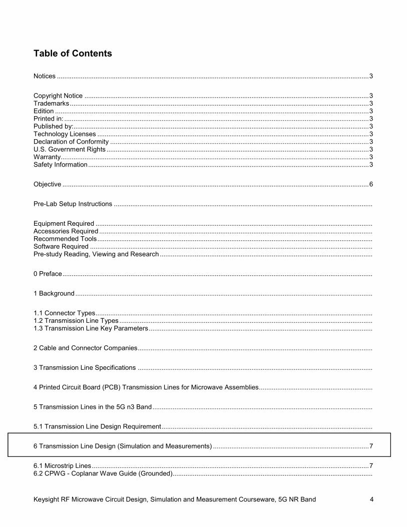
Table of Contents
Notices .......................................................................................................................................................................... 3
Copyright Notice ........................................................................................................................................................... 3 Trademarks ................................................................................................................................................................... 3 Edition ........................................................................................................................................................................... 3 Printed in: ...................................................................................................................................................................... 3 Published by:................................................................................................................................................................. 3 Technology Licenses .................................................................................................................................................... 3 Declaration of Conformity ............................................................................................................................................. 3 U.S. Government Rights ............................................................................................................................................... 3 Warranty ........................................................................................................................................................................ 3 Safety Information ......................................................................................................................................................... 3
Objective ....................................................................................................................................................................... 6
Pre-Lab Setup Instructions .............................................................................................................................................
Equipment Required ....................................................................................................................................................... Accessories Required ..................................................................................................................................................... Recommended Tools ...................................................................................................................................................... Software Required .......................................................................................................................................................... Pre-study Reading, Viewing and Research ....................................................................................................................
0 Preface .........................................................................................................................................................................
1 Background ..................................................................................................................................................................
1.1 Connector Types ....................................................................................................................................................... 1.2 Transmission Line Types .......................................................................................................................................... 1.3 Transmission Line Key Parameters ..........................................................................................................................
2 Cable and Connector Companies ................................................................................................................................
3 Transmission Line Specifications ................................................................................................................................
4 Printed Circuit Board (PCB) Transmission Lines for Microwave Assemblies ..............................................................
5 Transmission Lines in the 5G n3 Band ........................................................................................................................
5.1 Transmission Line Design Requirement ...................................................................................................................
6 Transmission Line Design (Simulation and Measurements) ..................................................................................... 7
6.1 Microstrip Lines ....................................................................................................................................................... 7 6.2 CPWG - Coplanar Wave Guide (Grounded) .............................................................................................................
Keysight RF Microwave Circuit Design, Simulation and Measurement Courseware, 5G NR Band 5
7 Measure the Performance of Physical Transmission Lines ..................................................................................... 20
7.1 Procedure to Measure Frequency Domain Performance of Transmission Lines ................................................. 20 7.2 Measurement Results for Transmission Lines...................................................................................................... 22 7.3 Procedure to Measure Time Domain for Cable and Connectors (Distance to Fault) ............................................... Measurement Results for Cable and Connectors ...........................................................................................................
Post-Lab Writeup ............................................................................................................................................................
References ......................................................................................................................................................................
Appendix A: FieldFox NA and CAT Calibration ..............................................................................................................
Background ..................................................................................................................................................................... Accessories Required ..................................................................................................................................................... Calibration Procedure ..................................................................................................................................................... Notes on CalRdy, Interpolation and Questionable Accuracy from the FieldFox Manual................................................ CalReady (displayed as CalRdy) .................................................................................................................................... Interpolation * .................................................................................................................................................................. Cal ON ? – Questionable Accuracy ................................................................................................................................
Appendix B: Saving Data on the FieldFox ......................................................................................................................
Saving with a USB Drive ................................................................................................................................................. Using BenchVue or FieldFox Data Link and FieldFox Remote Display to Control, Get Screens or Get Data ...............
Appendix C: Error Launching EMPro ..............................................................................................................................
Keysight RF Microwave Circuit Design, Simulation and Measurement Courseware, 5G NR Band 6
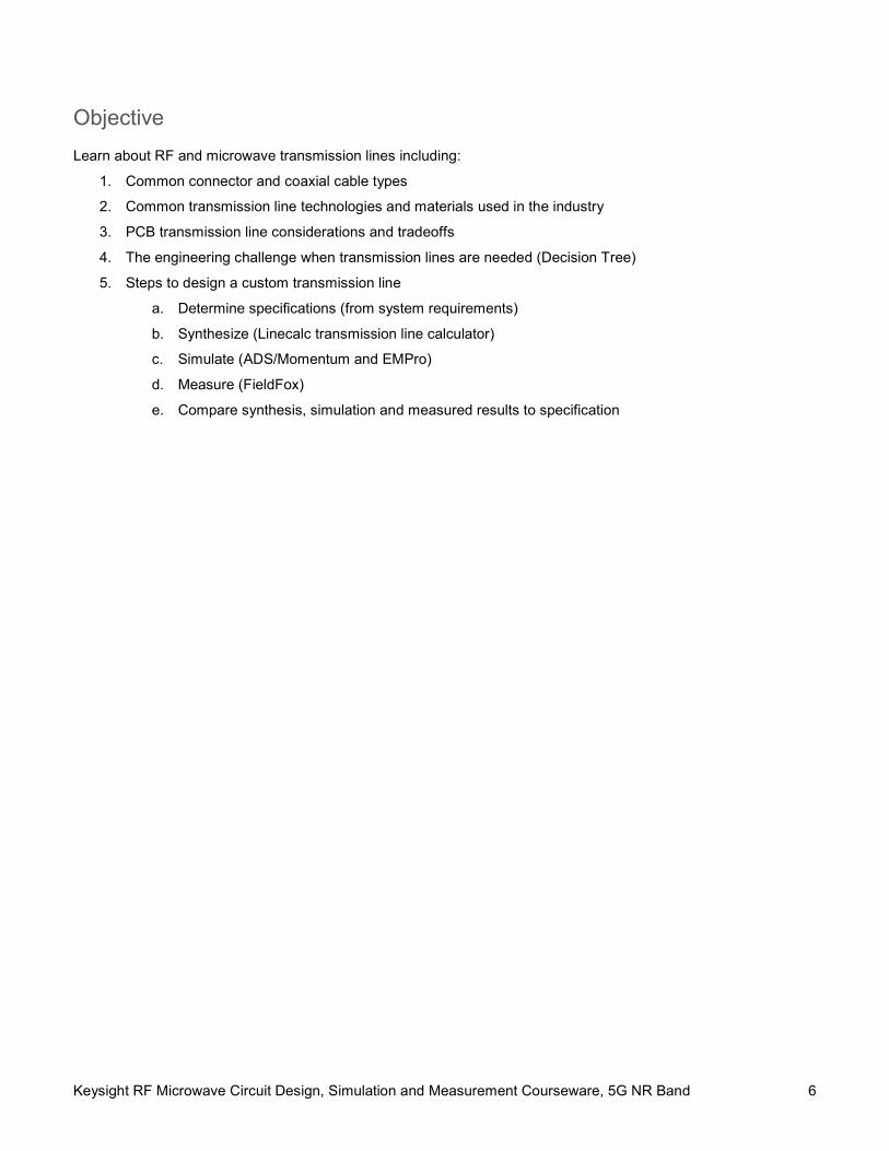
Objective
Learn about RF and microwave transmission lines including:
1. Common connector and coaxial cable types
2. Common transmission line technologies and materials used in the industry
3. PCB transmission line considerations and tradeoffs
4. The engineering challenge when transmission lines are needed (Decision Tree)
5. Steps to design a custom transmission line
a. Determine specifications (from system requirements)
b. Synthesize (Linecalc transmission line calculator)
c. Simulate (ADS/Momentum and EMPro)
d. Measure (FieldFox)
e. Compare synthesis, simulation and measured results to specification
Keysight RF Microwave Circuit Design, Simulation and Measurement Courseware, 5G NR Band 7
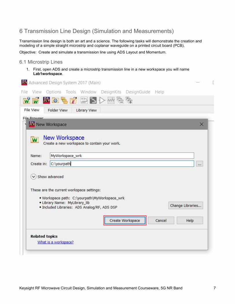
6 Transmission Line Design (Simulation and Measurements)
Transmission line design is both an art and a science. The following tasks will demonstrate the creation and modeling of a simple straight microstrip and coplanar waveguide on a printed circuit board (PCB).
Objective: Create and simulate a transmission line using ADS Layout and Momentum.
6.1 Microstrip Lines
1. First, open ADS and create a microstrip transmission line in a new workspace you will name Lab1workspace.
Keysight RF Microwave Circuit Design, Simulation and Measurement Courseware, 5G NR Band 8
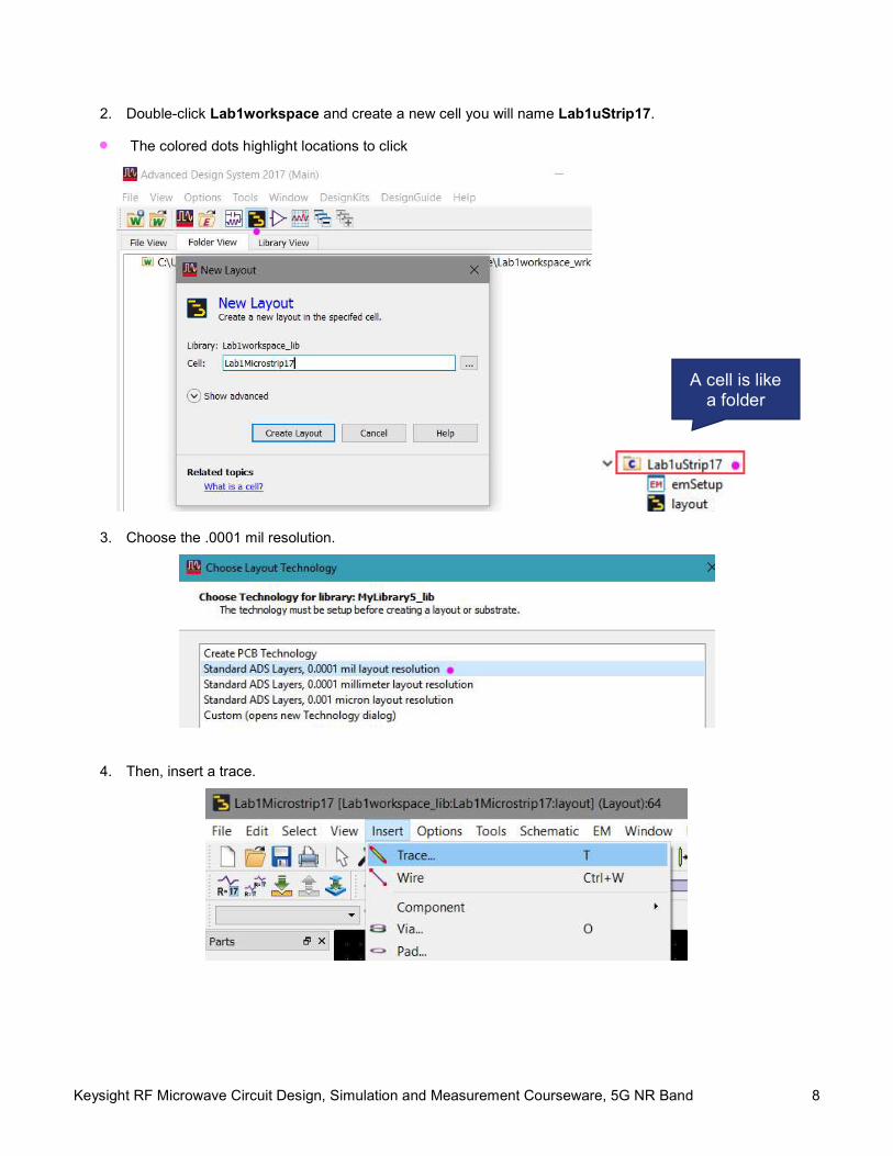
2. Double-click Lab1workspace and create a new cell you will name Lab1uStrip17.
The colored dots highlight locations to click
3. Choose the .0001 mil resolution.
4. Then, insert a trace.
A cell is like a folder
Keysight RF Microwave Circuit Design, Simulation and Measurement Courseware, 5G NR Band 9
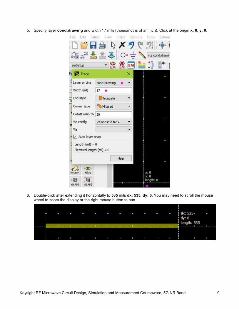
5. Specify layer cond:drawing and width 17 mils (thousandths of an inch). Click at the origin x: 0, y: 0.
6. Double-click after extending it horizontally to 535 mils dx: 535, dy: 0. You may need to scroll the mouse wheel to zoom the display or the right mouse button to pan.
Keysight RF Microwave Circuit Design, Simulation and Measurement Courseware, 5G NR Band 10
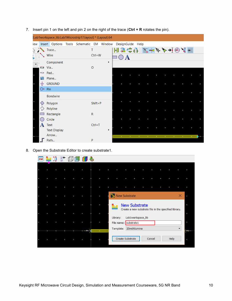
7. Insert pin 1 on the left and pin 2 on the right of the trace (Ctrl + R rotates the pin).
8. Open the Substrate Editor to create substrate1.
Keysight RF Microwave Circuit Design, Simulation and Measurement Courseware, 5G NR Band 11
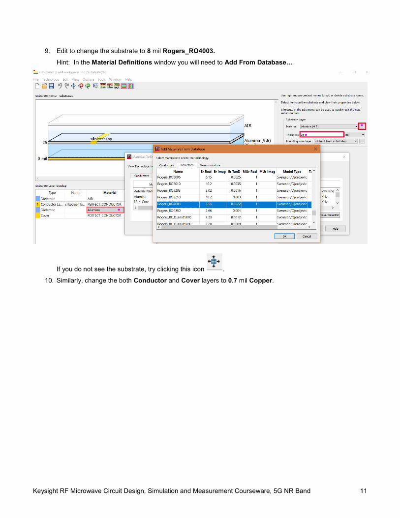
9. Edit to change the substrate to 8 mil Rogers_RO4003.
Hint: In the Material Definitions window you will need to Add From Database…
If you do not see the substrate, try clicking this icon .
10. Similarly, change the both Conductor and Cover layers to 0.7 mil Copper.
Keysight RF Microwave Circuit Design, Simulation and Measurement Courseware, 5G NR Band 12
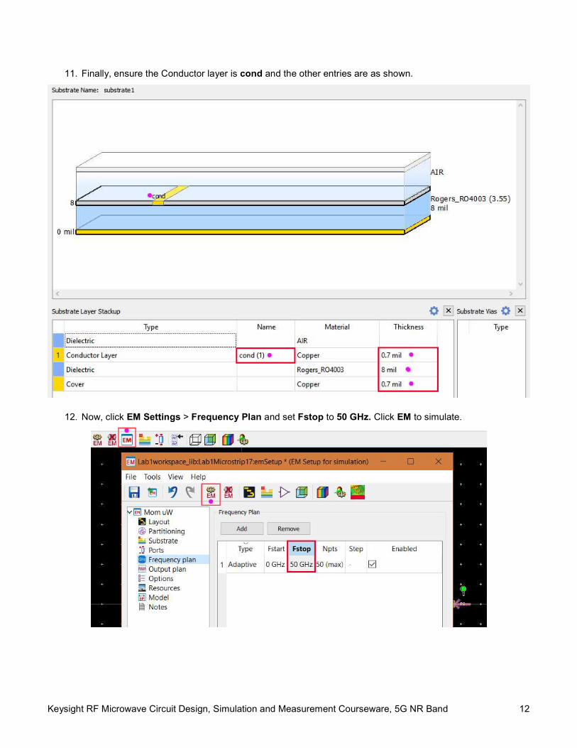
11. Finally, ensure the Conductor layer is cond and the other entries are as shown.
12. Now, click EM Settings > Frequency Plan and set Fstop to 50 GHz. Click EM to simulate.
Keysight RF Microwave Circuit Design, Simulation and Measurement Courseware, 5G NR Band 13
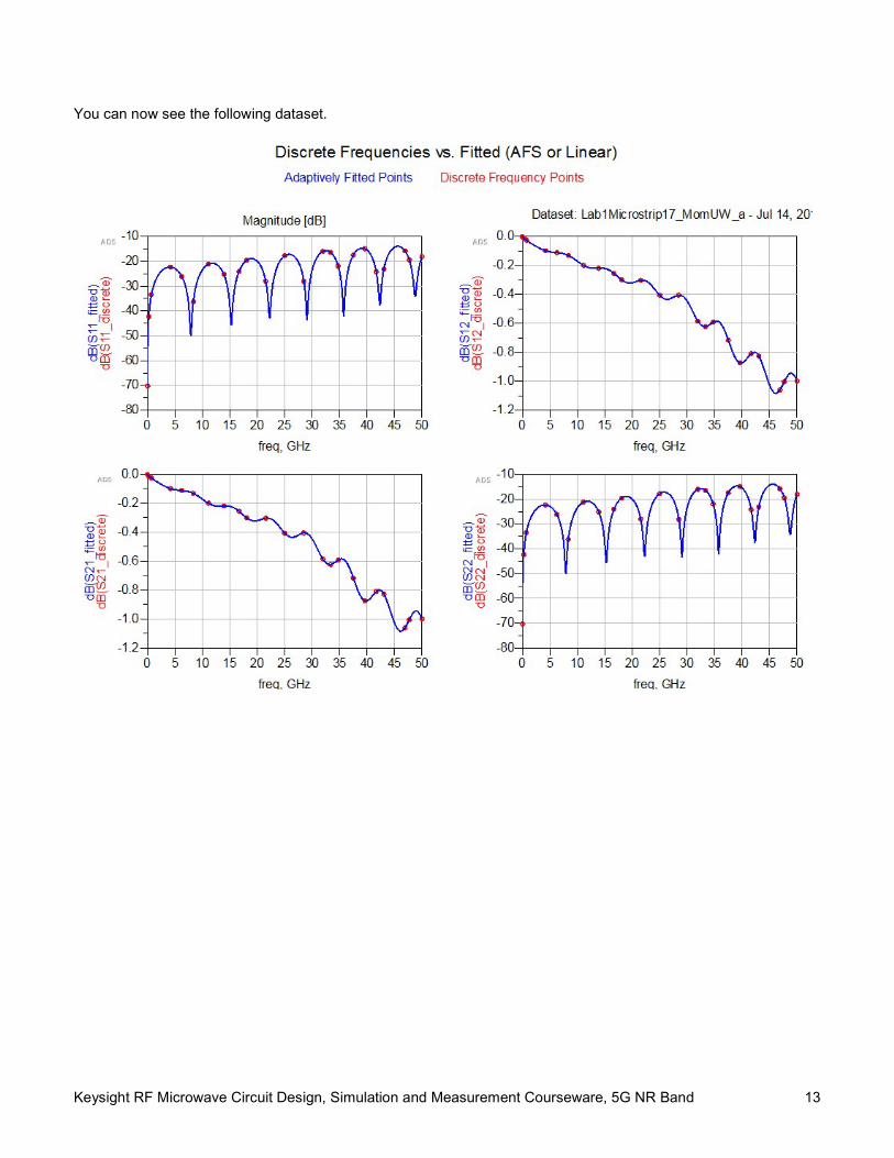
You can now see the following dataset.
Keysight RF Microwave Circuit Design, Simulation and Measurement Courseware, 5G NR Band 14
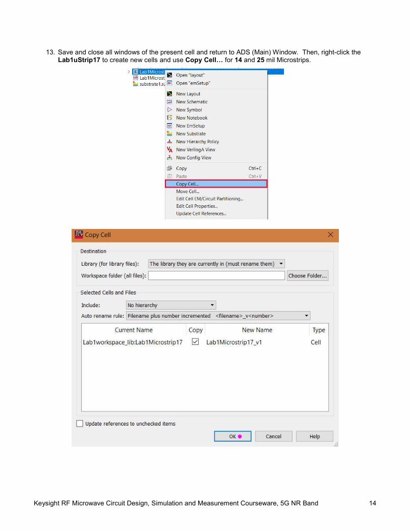
13. Save and close all windows of the present cell and return to ADS (Main) Window. Then, right-click the Lab1uStrip17 to create new cells and use Copy Cell… for 14 and 25 mil Microstrips.
Keysight RF Microwave Circuit Design, Simulation and Measurement Courseware, 5G NR Band 15
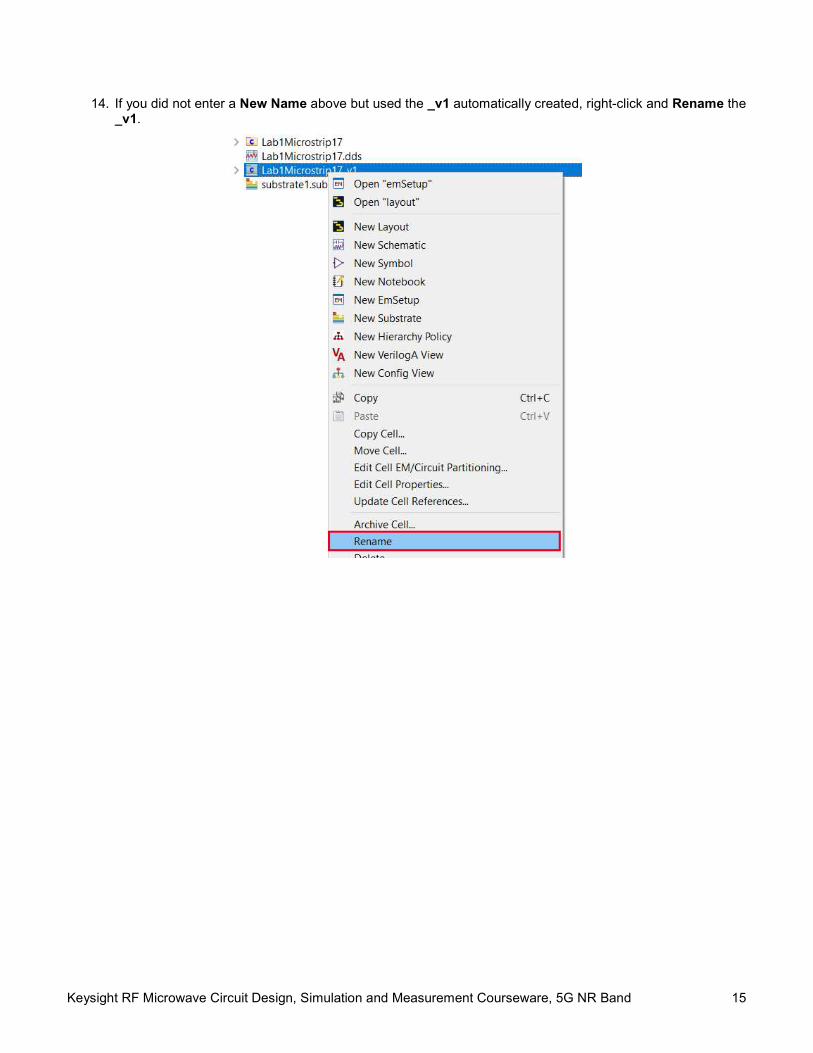
14. If you did not enter a New Name above but used the _v1 automatically created, right-click and Rename the _v1.
Keysight RF Microwave Circuit Design, Simulation and Measurement Courseware, 5G NR Band 16
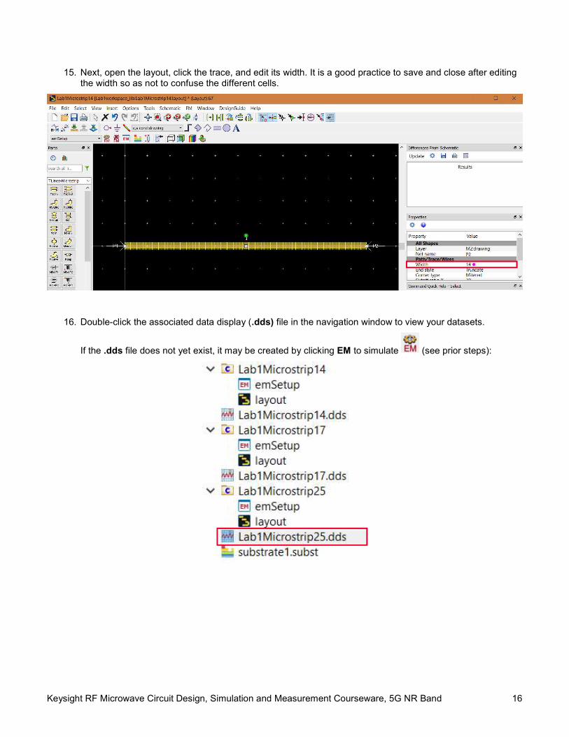
15. Next, open the layout, click the trace, and edit its width. It is a good practice to save and close after editing the width so as not to confuse the different cells.
16. Double-click the associated data display (.dds) file in the navigation window to view your datasets.
If the .dds file does not yet exist, it may be created by clicking EM to simulate (see prior steps):
Keysight RF Microwave Circuit Design, Simulation and Measurement Courseware, 5G NR Band 17
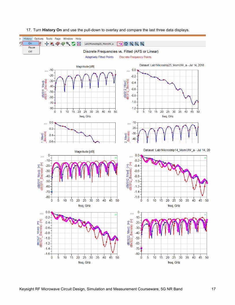
17. Turn History On and use the pull-down to overlay and compare the last three data displays.
Keysight RF Microwave Circuit Design, Simulation and Measurement Courseware, 5G NR Band 18
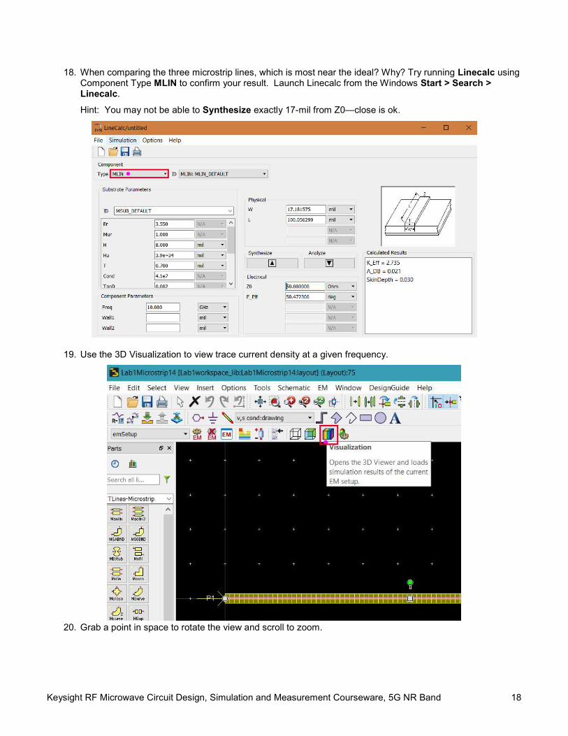
18. When comparing the three microstrip lines, which is most near the ideal? Why? Try running Linecalc using Component Type MLIN to confirm your result. Launch Linecalc from the Windows Start > Search > Linecalc.
Hint: You may not be able to Synthesize exactly 17-mil from Z0—close is ok.
19. Use the 3D Visualization to view trace current density at a given frequency.
20. Grab a point in space to rotate the view and scroll to zoom.
Keysight RF Microwave Circuit Design, Simulation and Measurement Courseware, 5G NR Band 19
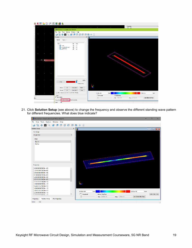
21. Click Solution Setup (see above) to change the frequency and observe the different standing wave pattern for different frequencies. What does blue indicate?
Keysight RF Microwave Circuit Design, Simulation and Measurement Courseware, 5G NR Band 20
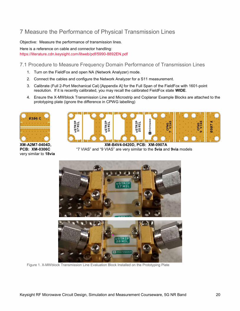
7 Measure the Performance of Physical Transmission Lines
Objective: Measure the performance of transmission lines.
Here is a reference on cable and connector handling: https://literature.cdn.keysight.com/litweb/pdf/5990-8892EN.pdf
7.1 Procedure to Measure Frequency Domain Performance of Transmission Lines 1. Turn on the FieldFox and open NA (Network Analyzer) mode.
2. Connect the cables and configure the Network Analyzer for a S11 measurement.
3. Calibrate (Full 2-Port Mechanical Cal) [Appendix A] for the Full Span of the FieldFox with 1601-point resolution. If it is recently calibrated, you may recall the calibrated FieldFox state WIDE.
4. Ensure the X-MWblock Transmission Line and Microstrip and Coplanar Example Blocks are attached to the prototyping plate (ignore the difference in CPWG labelling)
XM-A2M7-0404D, XM-B4V4-0420D, PCB: XM-0907A PCB: XM-0306C “7 VIAS” and “9 VIAS” are very similar to the 5via and 9via models very similar to 18via
Figure 1. X-MWblock Transmission Line Evaluation Block Installed on the Prototyping Plate
Keysight RF Microwave Circuit Design, Simulation and Measurement Courseware, 5G NR Band 21
5. Attach two X-MWprobes to the first of five lines which you simulated as Lab1uStrip17 and connect cables.
6. You may find it useful to use Keysight BenchVue to record measurements. For more information, see the Appendix.
7. Record numeric results on the table below.
8. Repeat for the remaining lines (see table below).
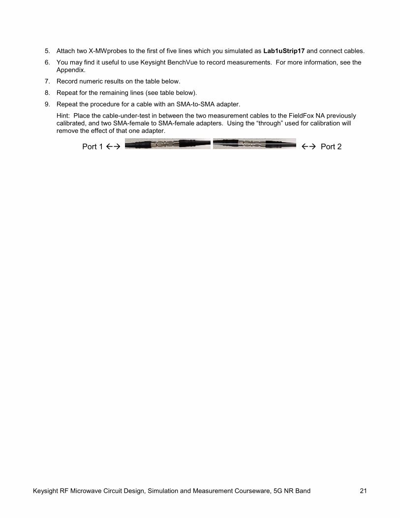
9. Repeat the procedure for a cable with an SMA-to-SMA adapter.
Hint: Place the cable-under-test in between the two measurement cables to the FieldFox NA previously calibrated, and two SMA-female to SMA-female adapters. Using the “through” used for calibration will remove the effect of that one adapter.
Port 1 Port 2
Keysight RF Microwave Circuit Design, Simulation and Measurement Courseware, 5G NR Band 22
7.2 Measurement Results for Transmission Lines Table 2. Transmission Line Results
Line Max Return Loss S11 to 4 GHz (dB)
Max Return Loss S11 to 12 GHz (dB)
Max Insertion Loss S21 to 4 GHz (dB)
Max Insertion Loss S21 to 12 GHz (dB)
Lab1uStrip17 Lab1uStrip14 Lab1uStrip25 Lab1CPWG17x11_5via Lab1CPWG17x11_9via Lab1CPWG17x11_18via 36-in Coaxial Cable 18-inch Coaxial Cable
Note for the last measurement you may need to change the scale to 0.3 dB/Div to measure cable loss.
1. How do the measured results compare with the Momentum simulations?
Note: The Keysight N9918A 26.5 GHz or N9950A 50 GHz FieldFox or equivalent NA will be required to resolve and observe via placement differences on the CPWG.
2. Open the completed EMPro simulation Lab1CPWG17x11_18via, Save the FieldFox measurement as an S2P file to the FieldFox Internal Device or USB Device, transfer to your computer using Keysight FieldFox Data Link (Send to PC) or a USB memory stick, then Read… it into the EMPro simulation for comparison. A sample Lab1CPWG17x11_18via.s2p is provided below.
Using Keysight FieldFox Data Link: Save, then Show, then Send to PC.
Keysight RF Microwave Circuit Design, Simulation and Measurement Courseware, 5G NR Band 23
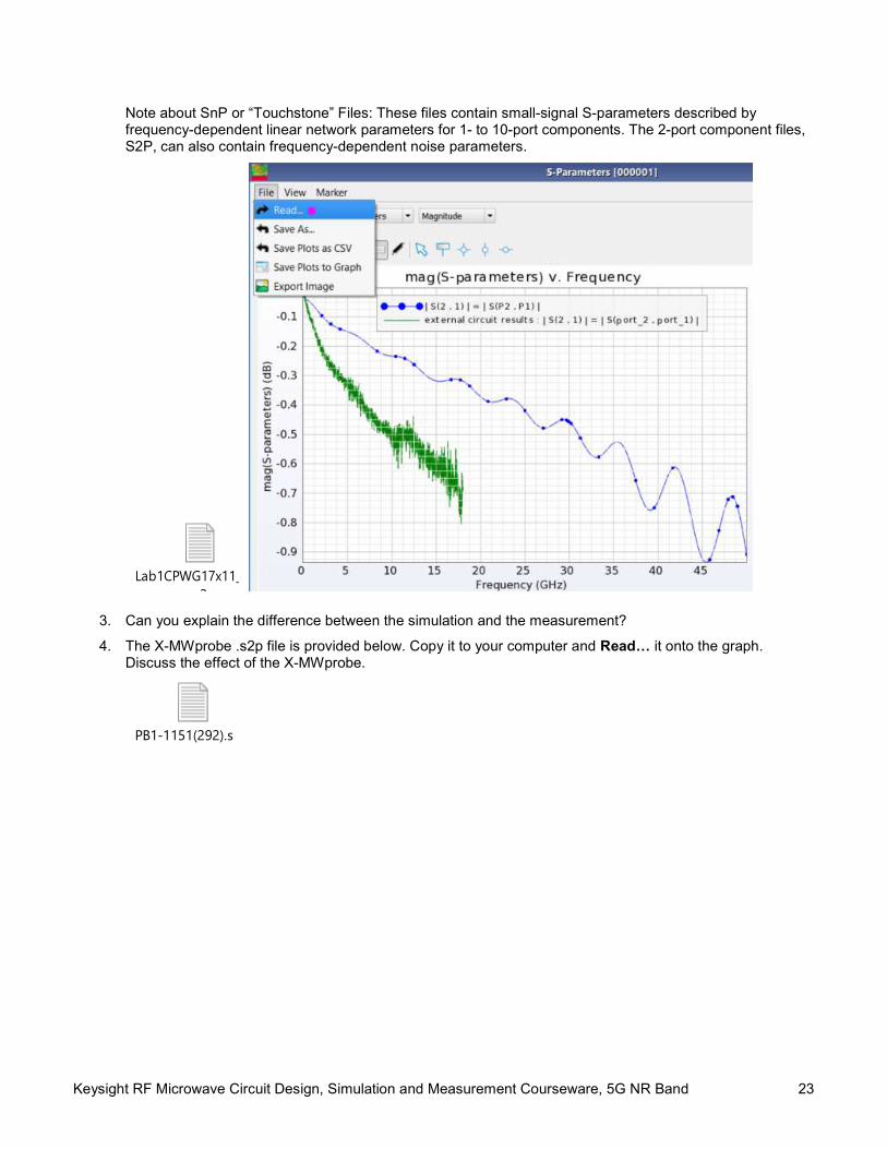
Note about SnP or “Touchstone” Files: These files contain small-signal S-parameters described by frequency-dependent linear network parameters for 1- to 10-port components. The 2-port component files, S2P, can also contain frequency-dependent noise parameters.
Lab1CPWG17x11_18vi
a.s2p
3. Can you explain the difference between the simulation and the measurement?
4. The X-MWprobe .s2p file is provided below. Copy it to your computer and Read… it onto the graph. Discuss the effect of the X-MWprobe.
PB1-1151(292).s2p
Keysight RF Microwave Circuit Design, Simulation and Measurement Courseware, 5G NR Band 24
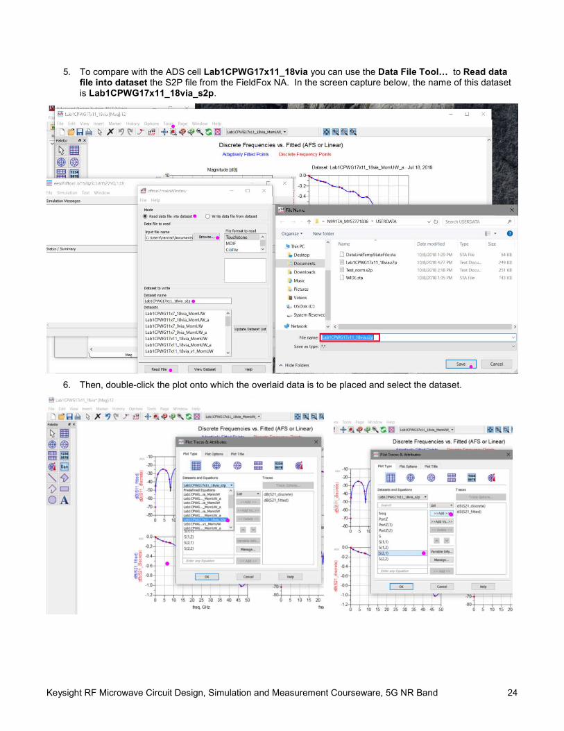
5. To compare with the ADS cell Lab1CPWG17x11_18via you can use the Data File Tool… to Read data file into dataset the S2P file from the FieldFox NA. In the screen capture below, the name of this dataset is Lab1CPWG17x11_18via_s2p.
6. Then, double-click the plot onto which the overlaid data is to be placed and select the dataset.
Keysight RF Microwave Circuit Design, Simulation and Measurement Courseware, 5G NR Band 25
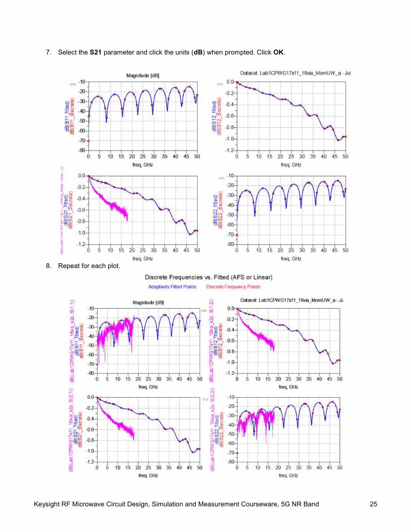
7. Select the S21 parameter and click the units (dB) when prompted. Click OK.
8. Repeat for each plot.
Keysight RF Microwave Circuit Design, Simulation and Measurement Courseware, 5G NR Band 26
Keysight RF Microwave Lab Courseware RF Microwave Circuit Design, Simulation and Measurement Courseware, 5G NR Band Lab 2: Filters
Lab Sheet

Keysight RF Microwave Circuit Design, Simulation and Measurement Courseware, 5G NR Band 27
Notices
Copyright Notice © Keysight Technologies 2019 No part of this manual may be reproduced in any form or by any means (including electronic storage and retrieval or translation into a foreign language) without prior agreement and written consent from Keysight Technologies as governed by United States and international copyright laws.
Edition Edition 1, May 2019
Printed in: Printed in Malaysia
All rights reserved. License terms – see www.keysight.com/find/courseware
Published by: Keysight Technologies Bayan Lepas Free Industrial Zone, 11900 Penang, Malaysia
Technology Licenses The hardware and/or software described in this document are furnished under a license and may be used or copied only in accordance with the terms of such license.
Declaration of Conformity Declarations of Conformity for this product and for other Keysight products may be downloaded from the Web. Go to http://www.keysight.com/go/conformity. You can then search by product number to find the latest Declaration of Conformity.
U.S. Government Rights The Software is “commercial computer software,” as defined by Federal Acquisition Regulation (“FAR”) 2.101. Pursuant to FAR 12.212 and 27.405-3 and Department of Defense FAR Supplement (“DFARS”) 227.7202, the U.S. government acquires commercial computer software under the same terms by which the software is customarily provided to the public. Accordingly, Keysight provides the Software to U.S. government customers under its standard commercial license, which is embodied in its End User License Agreement (EULA), a copy of which can be found at http://www.keysight.com/find/sweula. The license set forth in the EULA represents the exclusive authority by which the U.S. gov-ernment may use, modify, distribute, or dis-close the Software. The EULA and the li-cense set forth therein, does not require or permit, among other things, that Keysight: (1) Furnish technical information related to commercial computer software or com-mercial computer software documentation that is not customarily provided to the public; or (2) Relinquish to, or otherwise provide, the government rights in excess of these rights customarily provided to the public to use, modify, reproduce, release, perform, display, or disclose commercial computer software or commercial computer software documentation. No additional government requirements beyond those set forth in the EULA shall apply, except to the extent that those terms, rights, or licenses are explicitly required from all providers of commercial computer software pursuant to the FAR and the DFARS and are set forth specifically in writing else- where in the EULA. Keysight shall be under no obligation to update, revise or otherwise modify the Software. With respect to any technical data as defined by FAR 2.101, pursuant to FAR 12.211 and 27.404.2 and DFARS 227.7102, the U.S. government acquires no greater than Limited Rights as defined in FAR 27.401 or DFAR 227.7103-5 (c), as applicable in any technical data.
Warranty THE MATERIAL CONTAINED IN THIS DOCUMENT IS PROVIDED “AS IS,” AND IS SUBJECT TO BEING CHANGED, WITHOUT NOTICE, IN FUTURE EDI-TIONS. FURTHER, TO THE MAXIMUM EXTENT PERMITTED BY APPLICABLE LAW, KEYSIGHT DISCLAIMS ALL WAR-RANTIES, EITHER EXPRESS OR IM-PLIED, WITH REGARD TO THIS MANU-AL AND ANY INFORMATION CON-TAINED HEREIN, INCLUD ING BUT NOT LIMITED TO THE IMPLIED WARRANTIES OF MERCHANTABILITY AND FITNESS FOR A PARTICULAR PURPOSE. KEYSIGHT SHALL NOT BE LIABLE FOR ERRORS OR FOR INCIDENTAL OR CONSEQUENTIAL DAMAGES IN CONNECTION WITH THE FURNISHING, USE, OR PERFORMANCE OF THIS DOCUMENT OR OF ANY INFORMATION CON- TAINED HEREIN. SHOULD KEYSIGHT AND THE USER HAVE A SEPARATE WRITTEN AGREEMENT WITH WAR-RANTY TERMS COVERING THE MATE-RIAL IN THIS DOCUMENT THAT CON-FLICT WITH THESE TERMS, THE WAR-RANTY TERMS IN THE SEPARATE AGREEMENT SHALL CONTROL.
Safety Information
CAUTION A CAUTION notice denotes a hazard. It calls attention to an operating procedure, practice, or the like that, if not correctly performed or adhered to, could result in damage to the product or loss of important data. Do not proceed beyond a CAUTION notice until the indicated conditions are fully understood and met.
WARNING A WARNING notice denotes a hazard. It calls attention to an operating procedure, practice, or the like that, if not correctly performed or adhered to, could result in personal injury or death. Do not proceed beyond a WARNING notice until the indicated conditions are fully understood and met.
Keysight RF Microwave Circuit Design, Simulation and Measurement Courseware, 5G NR Band 28
Table of Contents
Notices ........................................................................................................................................................................ 27
Copyright Notice ......................................................................................................................................................... 27 Edition ......................................................................................................................................................................... 27 Printed in: .................................................................................................................................................................... 27 Published by:............................................................................................................................................................... 27 Technology Licenses .................................................................................................................................................. 27 Declaration of Conformity ........................................................................................................................................... 27 U.S. Government Rights ............................................................................................................................................. 27 Warranty ...................................................................................................................................................................... 27 Safety Information ....................................................................................................................................................... 27
Objective ..................................................................................................................................................................... 30
Pre-Lab Setup Instructions .............................................................................................................................................
Equipment Required ....................................................................................................................................................... Accessories Required ..................................................................................................................................................... Recommended Tools ...................................................................................................................................................... Software Required .......................................................................................................................................................... Pre-study reading and viewing........................................................................................................................................
1 Background ..................................................................................................................................................................
2 Filter Specifications ......................................................................................................................................................
3 Common Filter Technologies (Physical Types and Attributes) ....................................................................................
4 Filter Companies ..........................................................................................................................................................
5 The Engineer’s Challenge ............................................................................................................................................
5.1 Single Mixer Converter Design Example .................................................................................................................. 5.2 RF and IF Filter Design Specifications .....................................................................................................................
6 Filter Design .................................................................................................................................................................
6.1 Evaluate Off-the-Shelf RF and IF Filter Choices ...................................................................................................... 6.1.1 Evaluate an LTCC Filter for the RF Filter .............................................................................................................. 6.1.2 Evaluate a BAW Filter for the RF Filter .................................................................................................................. 6.1.3 Evaluate a SAW Device for the IF Filter ................................................................................................................ 6.2 Design a Lumped Element Low Pass Filter for the IF Filter ..................................................................................... 6.2.1 Synthesize the Lumped Element Filter .................................................................................................................. 6.2.2 Run Pre-prepared Inductor Simulations ................................................................................................................ 6.2.3 Run the Pre-prepared Low Pass Filter Simulation ................................................................................................ 6.2.4 Open in EMPro to Understand Filter Response ....................................................................................................
Keysight RF Microwave Circuit Design, Simulation and Measurement Courseware, 5G NR Band 29
7 Measure the Performance of the Built Low Pass Filter ........................................................................................... 31
7.1 Procedure to Measure the Filter Performance...................................................................................................... 31 7.2 Plot Synthesized, Simulated and Measured Data on the Same Plot ................................................................... 33 7.3 Tune the LPF by Hand .......................................................................................................................................... 34 7.4 Select the IF Filter ................................................................................................................................................. 34
Post-Lab Writeup ........................................................................................................................................................ 35
Appendix A: FieldFox Calibration................................................................................................................................ 36
Appendix B: Saving Data on the FieldFox .................................................................................................................. 37

Keysight RF Microwave Circuit Design, Simulation and Measurement Courseware, 5G NR Band 30
Objective
In this lab, you will learn about RF and microwave filters including:
6. Ideal filter response versus real world
7. Common filter technologies used in industry (close-up and In-production assembly)
8. Filter companies and types of filters offered
9. Filter specifications
After this introductory information about filters, you will use a design specification as you design, synthesize, simulate, build and verify performance:
10. The Engineering Challenge – Decision Tree
11. Steps to design a custom filter (168.5 MHz lumped element filter)
a. Determine specifications from system requirement
b. Synthesize (Genesys Synthesis)
c. Simulate (ADS/Momentum and EMpro)
d. Prototype / Tune (X-MWblock on Prototype Station)
e. Measure (FieldFox)
f. Compare synthesis, simulation, and measurements to specification
Keysight RF Microwave Circuit Design, Simulation and Measurement Courseware, 5G NR Band 31
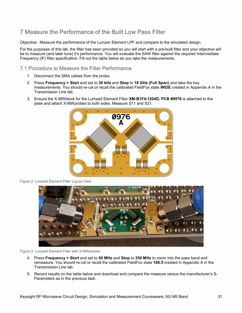
7 Measure the Performance of the Built Low Pass Filter
Objective: Measure the performance of the Lumper Element LPF and compare to the simulated design.
For the purposes of this lab, the filter has been provided so you will start with a pre-built filter and your objective will be to measure (and later tune) it’s performance. You will evaluate the SAW filter against the required Intermediate Frequency (IF) filter specification. Fill out the table below as you take the measurements.
7.1 Procedure to Measure the Filter Performance
1. Disconnect the SMA cables from the probe.
2. Press Frequency > Start and set to 30 kHz and Stop to 18 GHz (Full Span) and take the key measurements. You should re-cal or recall the calibrated FieldFox state WIDE created in Appendix A in the Transmission Line lab.
3. Ensure the X-MWblock for the Lumped Element Filter XM-B1F4-1204D, PCB #0976 is attached to the plate and attach X-MWprobes to both sides. Measure S11 and S21.
Figure 2. Lumped Element Filter Layout View
Figure 3. Lumped Element Filter with X-MWprobes
4. Press Frequency > Start and set to 50 MHz and Stop to 350 MHz to zoom into the pass band and remeasure. You should re-cal or recall the calibrated FieldFox state 168.5 created in Appendix A in the Transmission Line lab.
5. Record results on the table below and download and compare the measure versus the manufacturer’s S-Parameters as in the previous task.
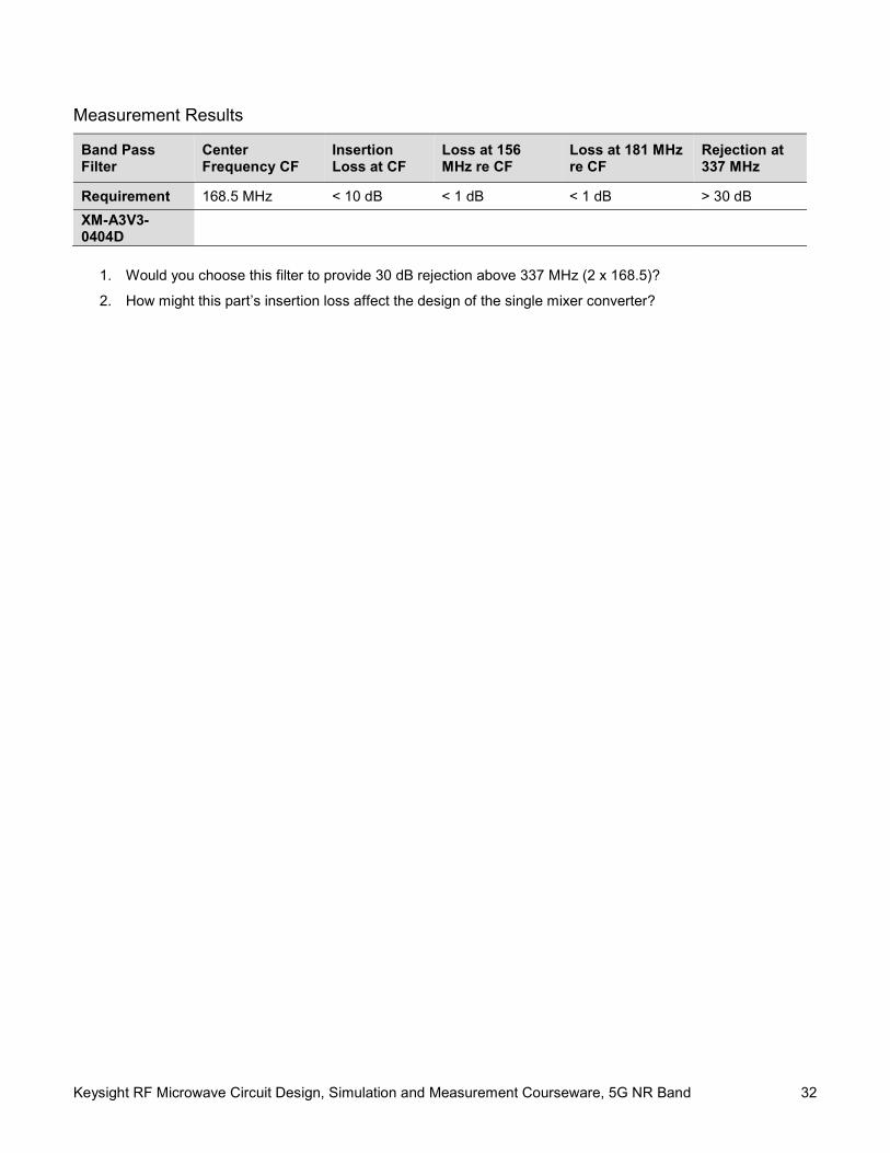
Keysight RF Microwave Circuit Design, Simulation and Measurement Courseware, 5G NR Band 32
Measurement Results
Band Pass Filter
Center Frequency CF
Insertion Loss at CF
Loss at 156 MHz re CF
Loss at 181 MHz re CF
Rejection at 337 MHz
Requirement 168.5 MHz < 10 dB < 1 dB < 1 dB > 30 dB
XM-A3V3-0404D
1. Would you choose this filter to provide 30 dB rejection above 337 MHz (2 x 168.5)?
2. How might this part’s insertion loss affect the design of the single mixer converter?
Keysight RF Microwave Circuit Design, Simulation and Measurement Courseware, 5G NR Band 33
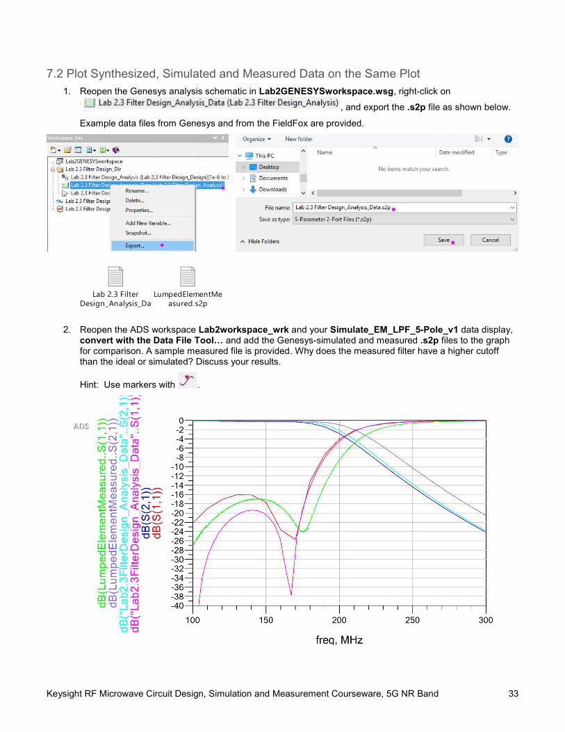
7.2 Plot Synthesized, Simulated and Measured Data on the Same Plot 1. Reopen the Genesys analysis schematic in Lab2GENESYSworkspace.wsg, right-click on
, and export the .s2p file as shown below.
Example data files from Genesys and from the FieldFox are provided.
Lab 2.3 Filter Design_Analysis_Data.s2p
LumpedElementMeasured.s2p
2. Reopen the ADS workspace Lab2workspace_wrk and your Simulate_EM_LPF_5-Pole_v1 data display,
convert with the Data File Tool… and add the Genesys-simulated and measured .s2p files to the graph for comparison. A sample measured file is provided. Why does the measured filter have a higher cutoff than the ideal or simulated? Discuss your results.
Hint: Use markers with .
Keysight RF Microwave Circuit Design, Simulation and Measurement Courseware, 5G NR Band 34
7.3 Tune the LPF by Hand
1. Ensure that you are displaying both S21 and S11 as large as possible on the same display effects.
2. Use a non-metallic pick (such as a toothpick) to gently and very-slightly spread the coils of the two inductors in the filter while watching the FieldFox display.
3. Press the coils closer together using two picks.
4. Describe the changes of the filter response.
7.4 Select the IF Filter Although the lumped element filter has better insertion loss and may have sufficient rejection at 337 MHz, its size and cost may make it unsuitable for use in mass-produced mobile systems. You will choose the second-best filter, the SAW filter, for the 5G n3 Receiver.
Since this filter has significantly higher insertion loss, how will the radio design proceed?

Keysight RF Microwave Circuit Design, Simulation and Measurement Courseware, 5G NR Band 35
Post-Lab Writeup
1. Provide screen captures of all measured data in a single document
2. Label each plot according to the lab step where it was captured.
3. If your results do not match your expectations, explain why.

Keysight RF Microwave Circuit Design, Simulation and Measurement Courseware, 5G NR Band 36
Appendix A: FieldFox Calibration
Please see Appendix in the first Lab Sheet.

Keysight RF Microwave Circuit Design, Simulation and Measurement Courseware, 5G NR Band 37
Appendix B: Saving Data on the FieldFox
Please see Appendix in the first Lab Sheet.
Page 38
Find us at www.keysight.com
Learn more at: www.keysight.com
For more information on Keysight Technologies’ products, applications or services, please contact your local Keysight office. The complete list is available at: www.keysight.com/find/contactus
This information is subject to change without notice. © Keysight Technologies, 2019, Published in USA, Aug 12, 2019, 5992-3916EN
Keysight RF Microwave Lab Courseware RF Microwave Circuit Design, Simulation and Measurement Courseware, 5G NR Band Lab 3: Low Noise Amplifiers (LNA)
Lab Sheet

Keysight RF Microwave Circuit Design, Simulation and Measurement Courseware, 5G NR Band 39
Notices
Copyright Notice © Keysight Technologies 2019 No part of this manual may be reproduced in any form or by any means (including electronic storage and retrieval or translation into a foreign language) without prior agreement and written consent from Keysight Technologies as governed by United States and international copyright laws.
Edition Edition 1, May 2019
Printed in: Printed in Malaysia
All rights reserved. License terms – see www.keysight.com/find/courseware
Published by: Keysight Technologies Bayan Lepas Free Industrial Zone, 11900 Penang, Malaysia
Technology Licenses The hardware and/or software described in this document are furnished under a license and may be used or copied only in accordance with the terms of such license.
Declaration of Conformity Declarations of Conformity for this product and for other Keysight products may be downloaded from the Web. Go to http://www.keysight.com/go/conformity. You can then search by product number to find the latest Declaration of Conformity.
U.S. Government Rights The Software is “commercial computer software,” as defined by Federal Acquisition Regulation (“FAR”) 2.101. Pursuant to FAR 12.212 and 27.405-3 and Department of Defense FAR Supplement (“DFARS”) 227.7202, the U.S. government acquires commercial computer software under the same terms by which the software is customarily provided to the public. Accordingly, Keysight provides the Software to U.S. government customers under its standard commercial license, which is embodied in its End User License Agreement (EULA), a copy of which can be found at http://www.keysight.com/find/sweula. The license set forth in the EULA represents the exclusive authority by which the U.S. gov-ernment may use, modify, distribute, or dis-close the Software. The EULA and the li-cense set forth therein, does not require or permit, among other things, that Keysight: (1) Furnish technical information related to commercial computer software or com-mercial computer software documentation that is not customarily provided to the public; or (2) Relinquish to, or otherwise provide, the government rights in excess of these rights customarily provided to the public to use, modify, reproduce, release, perform, display, or disclose commercial computer software or commercial computer software documentation. No additional government requirements beyond those set forth in the EULA shall apply, except to the extent that those terms, rights, or licenses are explicitly required from all providers of commercial computer software pursuant to the FAR and the DFARS and are set forth specifically in writing else- where in the EULA. Keysight shall be under no obligation to update, revise or otherwise modify the Software. With respect to any technical data as defined by FAR 2.101, pursuant to FAR 12.211 and 27.404.2 and DFARS 227.7102, the U.S. government acquires no greater than Limited Rights as defined in FAR 27.401 or DFAR 227.7103-5 (c), as applicable in any technical data.
Warranty THE MATERIAL CONTAINED IN THIS DOCUMENT IS PROVIDED “AS IS,” AND IS SUBJECT TO BEING CHANGED, WITHOUT NOTICE, IN FUTURE EDI-TIONS. FURTHER, TO THE MAXIMUM EXTENT PERMITTED BY APPLICABLE LAW, KEYSIGHT DISCLAIMS ALL WAR-RANTIES, EITHER EXPRESS OR IM-PLIED, WITH REGARD TO THIS MANU-AL AND ANY INFORMATION CON-TAINED HEREIN, INCLUD ING BUT NOT LIMITED TO THE IMPLIED WARRANTIES OF MERCHANTABILITY AND FITNESS FOR A PARTICULAR PURPOSE. KEYSIGHT SHALL NOT BE LIABLE FOR ERRORS OR FOR INCIDENTAL OR CONSEQUENTIAL DAMAGES IN CONNECTION WITH THE FURNISHING, USE, OR PERFORMANCE OF THIS DOCUMENT OR OF ANY INFORMATION CON- TAINED HEREIN. SHOULD KEYSIGHT AND THE USER HAVE A SEPARATE WRITTEN AGREEMENT WITH WAR-RANTY TERMS COVERING THE MATE-RIAL IN THIS DOCUMENT THAT CON-FLICT WITH THESE TERMS, THE WAR-RANTY TERMS IN THE SEPARATE AGREEMENT SHALL CONTROL.
Safety Information
CAUTION A CAUTION notice denotes a hazard. It calls attention to an operating procedure, practice, or the like that, if not correctly performed or adhered to, could result in damage to the product or loss of important data. Do not proceed beyond a CAUTION notice until the indicated conditions are fully understood and met.
WARNING A WARNING notice denotes a hazard. It calls attention to an operating procedure, practice, or the like that, if not correctly performed or adhered to, could result in personal injury or death. Do not proceed beyond a WARNING notice until the indicated conditions are fully understood and met.
Keysight RF Microwave Circuit Design, Simulation and Measurement Courseware, 5G NR Band 40
Table of Contents
Notices ........................................................................................................................................................................ 39
Copyright Notice ......................................................................................................................................................... 39 Edition ......................................................................................................................................................................... 39 Printed in: .................................................................................................................................................................... 39 Published by:............................................................................................................................................................... 39 Technology Licenses .................................................................................................................................................. 39 Declaration of Conformity ........................................................................................................................................... 39 U.S. Government Rights ............................................................................................................................................. 39 Warranty ...................................................................................................................................................................... 39 Safety Information ....................................................................................................................................................... 39
Objective ..................................................................................................................................................................... 42
Pre-Lab Setup Instructions .............................................................................................................................................
Equipment Required ....................................................................................................................................................... Accessories Required ..................................................................................................................................................... Recommended Tools ...................................................................................................................................................... Software Required .......................................................................................................................................................... Pre-Study Reading and Viewing .....................................................................................................................................
1 Background ..................................................................................................................................................................
2 Common Amplifier Types .............................................................................................................................................
3 Amplifier Performance Parameters ..............................................................................................................................
4 Amplifier Companies ....................................................................................................................................................
5 The Engineer’s Challenge - LNA Selection, Simulation and Measurement ................................................................
5.1 Single Mixer Converter Design Example .................................................................................................................. 5.2 LNA Design Requirement .........................................................................................................................................
6 Simulate and Measure the LNA ............................................................................................................................... 43
6.1 Create a Simple Simulation Model of an LNA ...................................................................................................... 43 6.1.0 Create a Model of the TQL9092 LNA and Simulate NF .................................................................................... 44 6.1.1 Examine the Effect of Attenuator Placement on NF .......................................................................................... 48 6.1.2 Explore Genesys Cascaded NF ........................................................................................................................ 49 6.1.3 Explore Simulations of Linearity – OIP3 ............................................................................................................ 51 6.1.4 Explore Simulations of Linearity – Gain Compression (OP1dB) ....................................................................... 54 6.2 Select from two Real LNAs ................................................................................................................................... 56 6.3 Set Up and Measure a Real Amplifier’s Supply Current ....................................................................................... 57 Procedure to Set Up and Measure Supply Current .................................................................................................... 57
Keysight RF Microwave Circuit Design, Simulation and Measurement Courseware, 5G NR Band 41
Results: Measured Supply Current ............................................................................................................................ 58 6.4 Measure a Real Amplifier’s Gain and Return Loss ................................................................................................... Procedure to Measure Gain and Return Loss ................................................................................................................ Results: Measured Gain and Return Loss ..................................................................................................................... 6.5 Measure a Real Amplifier’s Noise Figure ................................................................................................................. Learn About the Spectrum Analyzer’s Pre-Amplifier (Preamp) ...................................................................................... Procedure to Measure Noise Figure ............................................................................................................................... Summary of Noise Figure Equations .............................................................................................................................. Results: Measured Noise Figure.................................................................................................................................... 6.6 Measure a Real Amplifier’s Linearity – Output Third-Order Intercept OIP3 ............................................................. Procedure to Measure OIP3 ........................................................................................................................................... Results: Measured OIP3 ................................................................................................................................................ 6.7 Measure a Real Amplifier’s Linearity – Gain Compression OP1dB ......................................................................... Procedure to Measure Gain Compression OP1dB ......................................................................................................... Results: Measured OP1dB ............................................................................................................................................ 6.8 Repeat the Measurements for the TQL9092 at 3.3 V (optional)............................................................................... 6.9 Repeat the Measurements for the ADL5611 (optional) ............................................................................................
Reference........................................................................................................................................................................
Appendix A – Configuring the LNA for Probing on the X-MWplate ................................................................................
Keysight RF Microwave Circuit Design, Simulation and Measurement Courseware, 5G NR Band 42
Objective
In this lab, you will learn about RF and microwave amplifiers including:
12. Ideal amplifier response versus real-world
13. Common amplifier technologies used in industry (close-up and In-production assembly)
14. Amplifier companies and types of amplifiers offered
15. Amplifier specifications
After this introductory information about amplifiers, you will simulate an ideal amplifier using a design specification and evaluate two industry devices with similar performance before selecting the most appropriate device. Then you will measure to verify performance.
16. Steps to select a Low Noise Amplifier (LNA)
a. Determine Specifications (from System Requirements)
b. Synthesize (Genesys Synthesis)
c. Simulate (ADS/Momentum)
d. Prototype (X-MWblock on Prototype Station)
e. Measure (FieldFox and Signal Analyzer)
f. Compare Simulation and Measurements to Specification
Keysight RF Microwave Circuit Design, Simulation and Measurement Courseware, 5G NR Band 43
6 Simulate and Measure the LNA
You will first develop a simple simulation of the TQL9092 LNA and use it evaluate performance in Genesys. You will then measure the typical LNA performance parameters and compare to the data sheet.
6.1 Create a Simple Simulation Model of an LNA
Objective: Synthesize an Ideal Amplifier and then change the characteristics to emulate real world Additive Noise and Linearity for the TQL9092.
Keysight Genesys employs different types of simulation including Linear, RF System (Spectrasys), and Harmonic Balance. In this lab, you will begin with Linear which is the fastest and simplest simulation for basic circuits and systems. You will simulate Gain, Return Loss, and Noise using Linear Simulation. Linear simulations are also referred to as small signal performance of the amplifier.
When you require the non-linear portion of the same amplifier model, you will change to RF System simulation. This will allow the use of Multi-source signal sources and non-linear characteristics such as Intermodulation Products (IP3), Gain Compression, and Saturation.
Please review this information on Genesys: https://www.keysight.com/en/pc-1297125/genesys-rf-and-microwave-design-software?nid=-34275.0.00&cc=US&lc=eng
In the future Mixer lab, you will use Harmonic Balance as it best predicts harmonics, mixing products and phase noise. For more information please see this:
https://www.keysight.com/main/editorial.jspx?cc=US&lc=eng&ckey=1823632&nid=-34275.0.00&id=1823632&cmpid=zzfindeesof-genesys-harbec
In addition, here is a video on Harmonic Balance in Genesys: https://www.youtube.com/watch?v=Q894CVTWU8E
Keysight RF Microwave Circuit Design, Simulation and Measurement Courseware, 5G NR Band 44
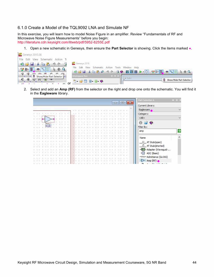
6.1.0 Create a Model of the TQL9092 LNA and Simulate NF
In this exercise, you will learn how to model Noise Figure in an amplifier. Review “Fundamentals of RF and Microwave Noise Figure Measurements” before you begin: http://literature.cdn.keysight.com/litweb/pdf/5952-8255E.pdf
1. Open a new schematic in Genesys, then ensure the Part Selector is showing. Click the items marked ●.
or
2. Select and add an Amp (RF) from the selector on the right and drop one onto the schematic. You will find it in the Eagleware library.
Keysight RF Microwave Circuit Design, Simulation and Measurement Courseware, 5G NR Band 45
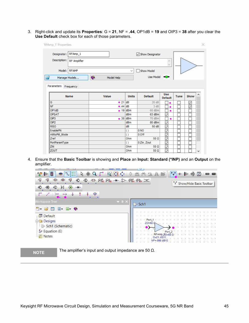
3. Right-click and update its Properties: G = 21, NF = .44, OP1dB = 19 and OIP3 = 38 after you clear the Use Default check box for each of those parameters.
4. Ensure that the Basic Toolbar is showing and Place an Input: Standard (*INP) and an Output on the
amplifier.
NOTE The amplifier’s input and output impedance are 50 Ω.
Keysight RF Microwave Circuit Design, Simulation and Measurement Courseware, 5G NR Band 46
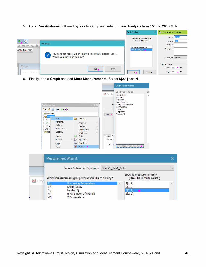
5. Click Run Analyses, followed by Yes to set up and select Linear Analysis from 1500 to 2000 MHz.
6. Finally, add a Graph and add More Measurements. Select S[2,1] and N.
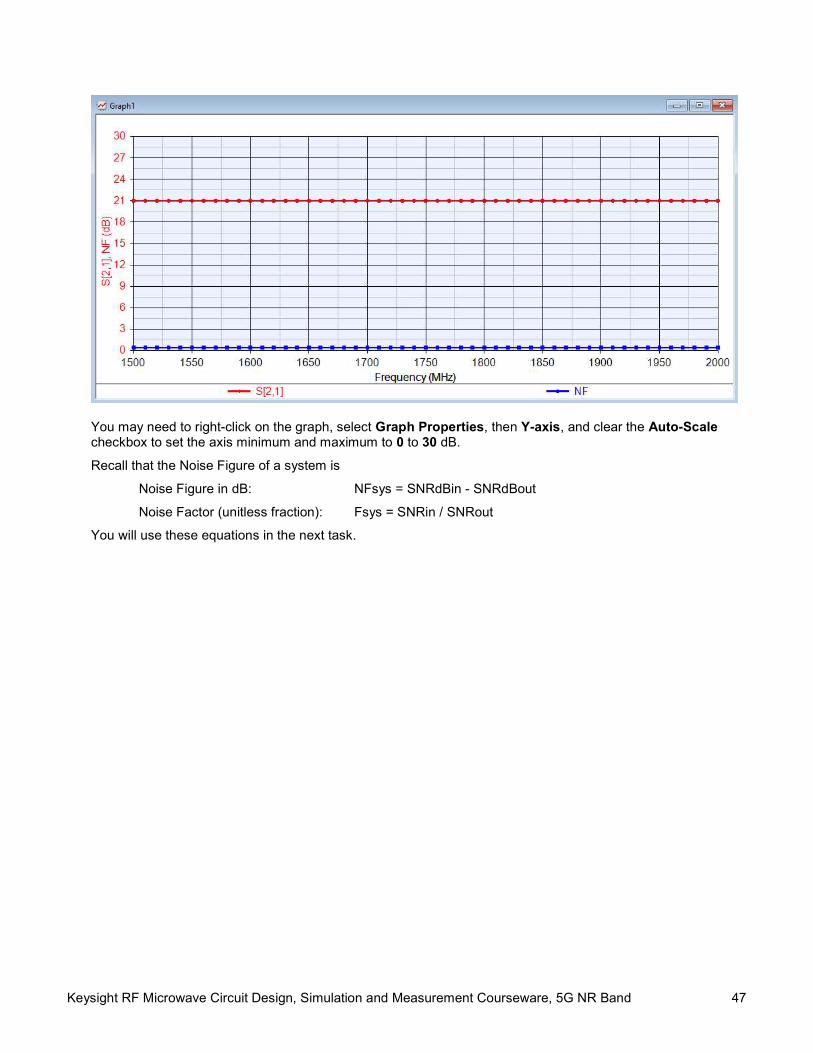
Keysight RF Microwave Circuit Design, Simulation and Measurement Courseware, 5G NR Band 47
You may need to right-click on the graph, select Graph Properties, then Y-axis, and clear the Auto-Scale checkbox to set the axis minimum and maximum to 0 to 30 dB.
Recall that the Noise Figure of a system is
Noise Figure in dB: NFsys = SNRdBin - SNRdBout
Noise Factor (unitless fraction): Fsys = SNRin / SNRout
You will use these equations in the next task.
Keysight RF Microwave Circuit Design, Simulation and Measurement Courseware, 5G NR Band 48
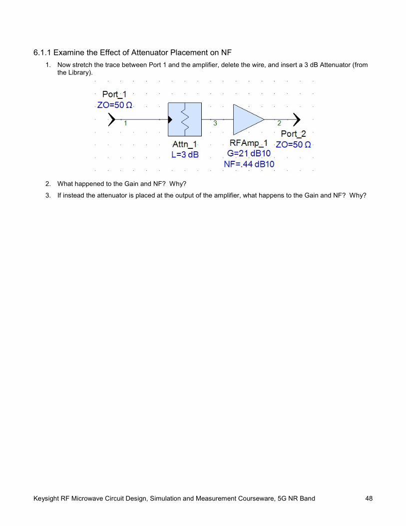
6.1.1 Examine the Effect of Attenuator Placement on NF
1. Now stretch the trace between Port 1 and the amplifier, delete the wire, and insert a 3 dB Attenuator (from the Library).
2. What happened to the Gain and NF? Why?
3. If instead the attenuator is placed at the output of the amplifier, what happens to the Gain and NF? Why?
Keysight RF Microwave Circuit Design, Simulation and Measurement Courseware, 5G NR Band 49
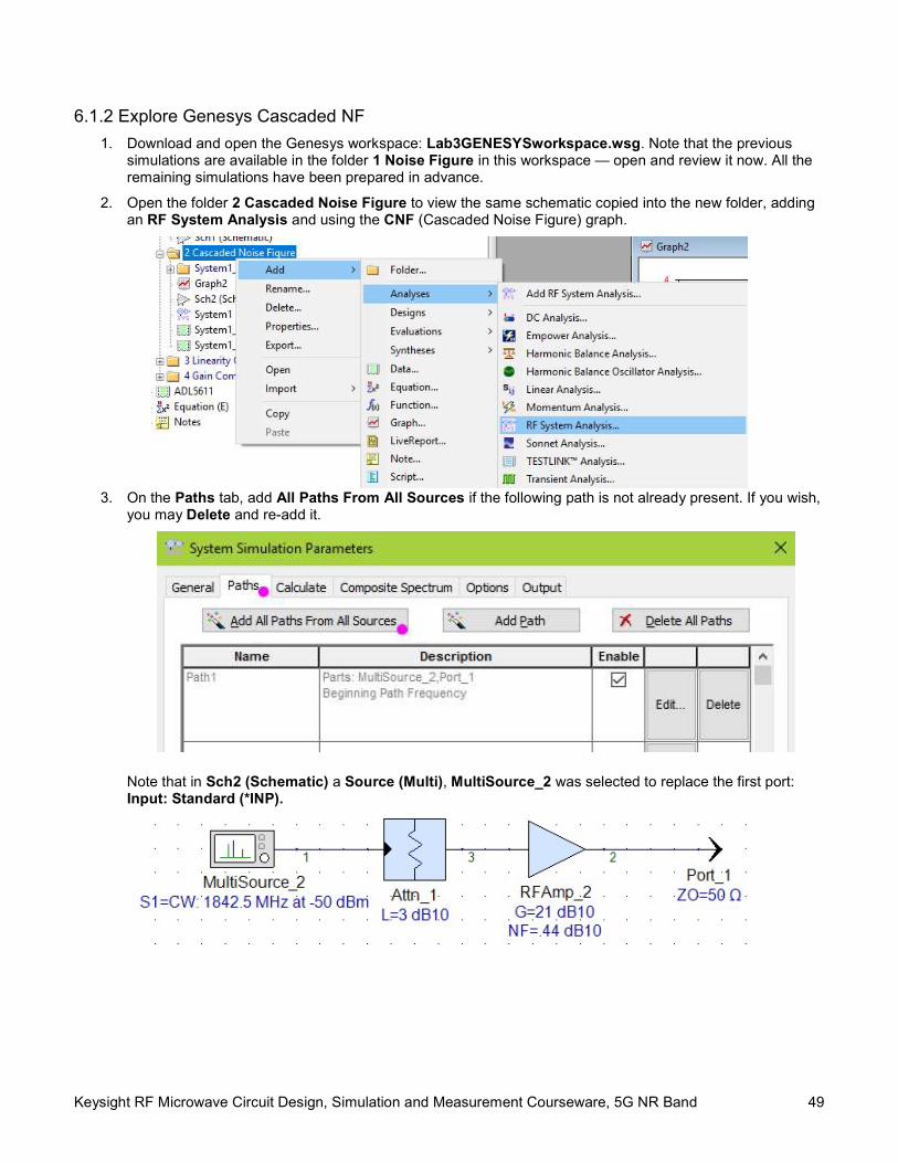
6.1.2 Explore Genesys Cascaded NF
1. Download and open the Genesys workspace: Lab3GENESYSworkspace.wsg. Note that the previous simulations are available in the folder 1 Noise Figure in this workspace — open and review it now. All the remaining simulations have been prepared in advance.
2. Open the folder 2 Cascaded Noise Figure to view the same schematic copied into the new folder, adding an RF System Analysis and using the CNF (Cascaded Noise Figure) graph.
3. On the Paths tab, add All Paths From All Sources if the following path is not already present. If you wish,
you may Delete and re-add it.
Note that in Sch2 (Schematic) a Source (Multi), MultiSource_2 was selected to replace the first port: Input: Standard (*INP).
Keysight RF Microwave Circuit Design, Simulation and Measurement Courseware, 5G NR Band 50
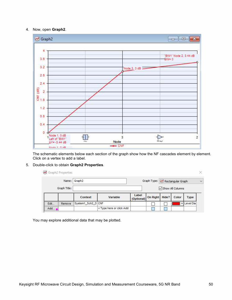
4. Now, open Graph2.
The schematic elements below each section of the graph show how the NF cascades element by element. Click on a vertex to add a label.
5. Double-click to obtain Graph2 Properties.
You may explore additional data that may be plotted.
Keysight RF Microwave Circuit Design, Simulation and Measurement Courseware, 5G NR Band 51
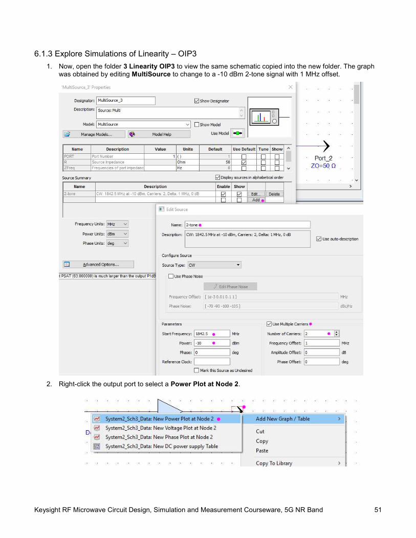
6.1.3 Explore Simulations of Linearity – OIP3
1. Now, open the folder 3 Linearity OIP3 to view the same schematic copied into the new folder. The graph was obtained by editing MultiSource to change to a -10 dBm 2-tone signal with 1 MHz offset.
2. Right-click the output port to select a Power Plot at Node 2.
Keysight RF Microwave Circuit Design, Simulation and Measurement Courseware, 5G NR Band 52
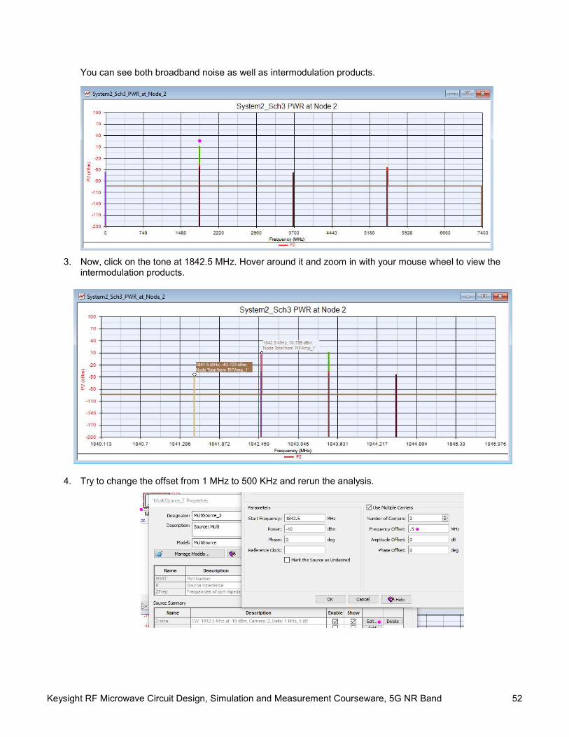
You can see both broadband noise as well as intermodulation products.
3. Now, click on the tone at 1842.5 MHz. Hover around it and zoom in with your mouse wheel to view the
intermodulation products.
4. Try to change the offset from 1 MHz to 500 KHz and rerun the analysis.
Keysight RF Microwave Circuit Design, Simulation and Measurement Courseware, 5G NR Band 53
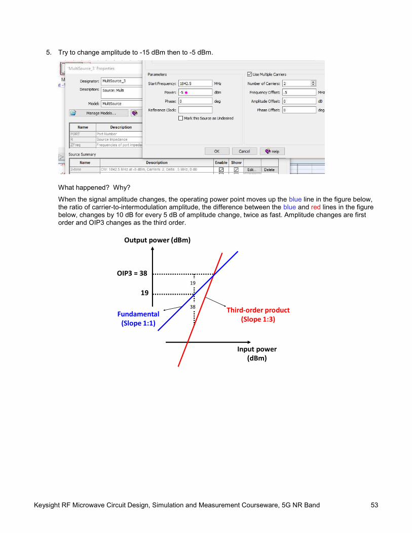
5. Try to change amplitude to -15 dBm then to -5 dBm.
What happened? Why?
When the signal amplitude changes, the operating power point moves up the blue line in the figure below, the ratio of carrier-to-intermodulation amplitude, the difference between the blue and red lines in the figure below, changes by 10 dB for every 5 dB of amplitude change, twice as fast. Amplitude changes are first order and OIP3 changes as the third order.
Output power (dBm)
Input power(dBm)
OIP3 = 38
1919
38Fundamental
(Slope 1:1)
Third-order product(Slope 1:3)
Keysight RF Microwave Circuit Design, Simulation and Measurement Courseware, 5G NR Band 54
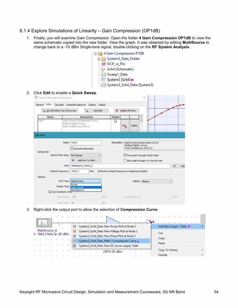
6.1.4 Explore Simulations of Linearity – Gain Compression (OP1dB)
1. Finally, you will examine Gain Compression. Open the folder 4 Gain Compression OP1dB to view the same schematic copied into the new folder. View the graph. It was obtained by editing MultiSource to change back to a -10 dBm Single-tone signal, double-clicking on the RF System Analysis.
2. Click Edit to enable a Quick Sweep.
3. Right-click the output port to allow the selection of Compression Curve.
Keysight RF Microwave Circuit Design, Simulation and Measurement Courseware, 5G NR Band 55
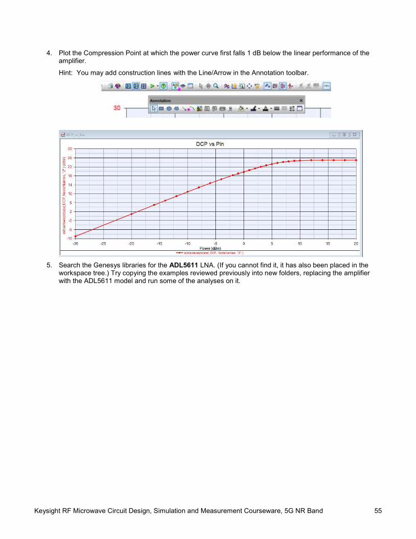
4. Plot the Compression Point at which the power curve first falls 1 dB below the linear performance of the amplifier.
Hint: You may add construction lines with the Line/Arrow in the Annotation toolbar.
5. Search the Genesys libraries for the ADL5611 LNA. (If you cannot find it, it has also been placed in the
workspace tree.) Try copying the examples reviewed previously into new folders, replacing the amplifier with the ADL5611 model and run some of the analyses on it.
Keysight RF Microwave Circuit Design, Simulation and Measurement Courseware, 5G NR Band 56
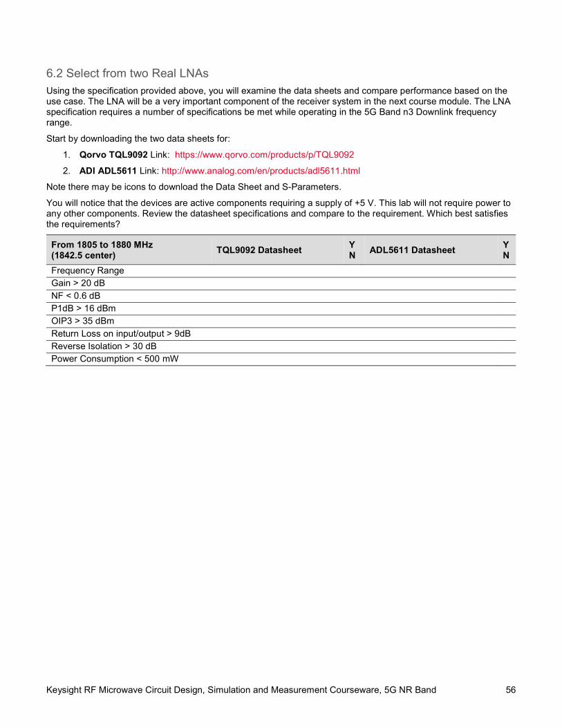
6.2 Select from two Real LNAs Using the specification provided above, you will examine the data sheets and compare performance based on the use case. The LNA will be a very important component of the receiver system in the next course module. The LNA specification requires a number of specifications be met while operating in the 5G Band n3 Downlink frequency range.
Start by downloading the two data sheets for:
1. Qorvo TQL9092 Link: https://www.qorvo.com/products/p/TQL9092
2. ADI ADL5611 Link: http://www.analog.com/en/products/adl5611.html
Note there may be icons to download the Data Sheet and S-Parameters.
You will notice that the devices are active components requiring a supply of +5 V. This lab will not require power to any other components. Review the datasheet specifications and compare to the requirement. Which best satisfies the requirements?
From 1805 to 1880 MHz (1842.5 center)
TQL9092 Datasheet Y N
ADL5611 Datasheet Y N
Frequency Range Gain > 20 dB NF < 0.6 dB P1dB > 16 dBm OIP3 > 35 dBm Return Loss on input/output > 9dB Reverse Isolation > 30 dB Power Consumption < 500 mW
Keysight RF Microwave Circuit Design, Simulation and Measurement Courseware, 5G NR Band 57
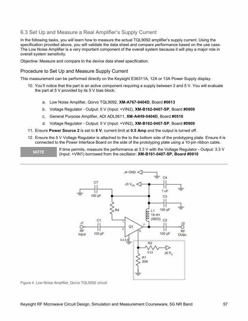
6.3 Set Up and Measure a Real Amplifier’s Supply Current In the following tasks, you will learn how to measure the actual TQL9092 amplifier’s supply current. Using the specification provided above, you will validate the data sheet and compare performance based on the use case. The Low Noise Amplifier is a very important component of the overall system because it will play a major role in overall system sensitivity.
Objective: Measure and compare to the device data sheet specification.
Procedure to Set Up and Measure Supply Current
This measurement can be performed directly on the Keysight E36311A, 12A or 13A Power Supply display.
10. You’ll notice that the part is an active component requiring a supply between 3 and 5 V. You will evaluate the part at 5 V provided by its 5 V bias block:
a. Low Noise Amplifier, Qorvo TQL9092, XM-A767-0404D, Board #0613
b. Voltage Regulator - Output: 5 V (Input: +VIN2), XM-B162-0407-SP, Board #0909
c. General Purpose Amplifier, ADI ADL5611, XM-A4H9-0404D, Board #0516
d. Voltage Regulator - Output: 5 V (Input: +VIN2), XM-B162-0407-SP, Board #0909
11. Ensure Power Source 2 is set to 6 V, current limit at 0.5 Amp and the output is turned off.
12. Ensure the 5 V Voltage Regulator is attached to the to the bottom side of the prototyping plate. Ensure it is connected to the Power Interface Board on the side of the prototyping plate using a 10-pin ribbon cable.
NOTE If time permits, measure the performance at 3.3 V with the Voltage Regulator - Output: 3.3 V (Input: +VIN1) borrowed from the oscillator: XM-B161-0407-SP, Board #0910
Figure 4. Low Noise Amplifier, Qorvo TQL9092 circuit
Keysight RF Microwave Circuit Design, Simulation and Measurement Courseware, 5G NR Band 58
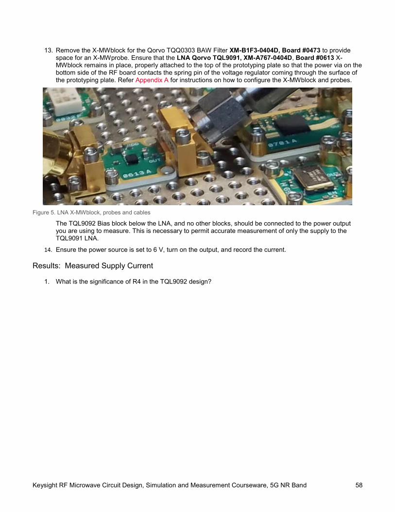
13. Remove the X-MWblock for the Qorvo TQQ0303 BAW Filter XM-B1F3-0404D, Board #0473 to provide space for an X-MWprobe. Ensure that the LNA Qorvo TQL9091, XM-A767-0404D, Board #0613 X-MWblock remains in place, properly attached to the top of the prototyping plate so that the power via on the bottom side of the RF board contacts the spring pin of the voltage regulator coming through the surface of the prototyping plate. Refer Appendix A for instructions on how to configure the X-MWblock and probes.
Figure 5. LNA X-MWblock, probes and cables
The TQL9092 Bias block below the LNA, and no other blocks, should be connected to the power output you are using to measure. This is necessary to permit accurate measurement of only the supply to the TQL9091 LNA.
14. Ensure the power source is set to 6 V, turn on the output, and record the current.
Results: Measured Supply Current
1. What is the significance of R4 in the TQL9092 design?
Keysight RF Microwave Circuit Design, Simulation and Measurement Courseware, 5G NR Band 59
Keysight RF Microwave Lab Courseware RF Microwave Circuit Design, Simulation and Measurement Courseware, 5G NR Band Lab 4: Driver and Power Amplifiers
Lab Sheet
Keysight RF Microwave Circuit Design, Simulation and Measurement Courseware, 5G NR Band 60
Notices
Copyright Notice © Keysight Technologies 2019 No part of this manual may be reproduced in any form or by any means (including electronic storage and retrieval or translation into a foreign language) without prior agreement and written consent from Keysight Technologies as governed by United States and international copyright laws.
Edition Edition 1, May 2019
Printed in: Printed in Malaysia
All rights reserved. License terms – see www.keysight.com/find/courseware
Published by: Keysight Technologies Bayan Lepas Free Industrial Zone, 11900 Penang, Malaysia
Technology Licenses The hardware and/or software described in this document are furnished under a license and may be used or copied only in accordance with the terms of such license.
Declaration of Conformity Declarations of Conformity for this product and for other Keysight products may be downloaded from the Web. Go to http://www.keysight.com/go/conformity. You can then search by product number to find the latest Declaration of Conformity.
U.S. Government Rights The Software is “commercial computer software,” as defined by Federal Acquisition Regulation (“FAR”) 2.101. Pursuant to FAR 12.212 and 27.405-3 and Department of Defense FAR Supplement (“DFARS”) 227.7202, the U.S. government acquires commercial computer software under the same terms by which the software is customarily provided to the public. Accordingly, Keysight provides the Software to U.S. government customers under its standard commercial license, which is embodied in its End User License Agreement (EULA), a copy of which can be found at http://www.keysight.com/find/sweula. The license set forth in the EULA represents the exclusive authority by which the U.S. gov-ernment may use, modify, distribute, or dis-close the Software. The EULA and the li-cense set forth therein, does not require or permit, among other things, that Keysight: (1) Furnish technical information related to commercial computer software or com-mercial computer software documentation that is not customarily provided to the public; or (2) Relinquish to, or otherwise provide, the government rights in excess of these rights customarily provided to the public to use, modify, reproduce, release, perform, display, or disclose commercial computer software or commercial computer software documentation. No additional government requirements beyond those set forth in the EULA shall apply, except to the extent that those terms, rights, or licenses are explicitly required from all providers of commercial computer software pursuant to the FAR and the DFARS and are set forth specifically in writing else- where in the EULA. Keysight shall be under no obligation to update, revise or otherwise modify the Software. With respect to any technical data as defined by FAR 2.101, pursuant to FAR 12.211 and 27.404.2 and DFARS 227.7102, the U.S. government acquires no greater than Limited Rights as defined in FAR 27.401 or DFAR 227.7103-5 (c), as applicable in any technical data.
Warranty THE MATERIAL CONTAINED IN THIS DOCUMENT IS PROVIDED “AS IS,” AND IS SUBJECT TO BEING CHANGED, WITHOUT NOTICE, IN FUTURE EDI-TIONS. FURTHER, TO THE MAXIMUM EXTENT PERMITTED BY APPLICABLE LAW, KEYSIGHT DISCLAIMS ALL WAR-RANTIES, EITHER EXPRESS OR IM-PLIED, WITH REGARD TO THIS MANU-AL AND ANY INFORMATION CON-TAINED HEREIN, INCLUD ING BUT NOT LIMITED TO THE IMPLIED WARRANTIES OF MERCHANTABILITY AND FITNESS FOR A PARTICULAR PURPOSE. KEYSIGHT SHALL NOT BE LIABLE FOR ERRORS OR FOR INCIDENTAL OR CONSEQUENTIAL DAMAGES IN CONNECTION WITH THE FURNISHING, USE, OR PERFORMANCE OF THIS DOCUMENT OR OF ANY INFORMATION CON- TAINED HEREIN. SHOULD KEYSIGHT AND THE USER HAVE A SEPARATE WRITTEN AGREEMENT WITH WAR-RANTY TERMS COVERING THE MATE-RIAL IN THIS DOCUMENT THAT CON-FLICT WITH THESE TERMS, THE WAR-RANTY TERMS IN THE SEPARATE AGREEMENT SHALL CONTROL.
Safety Information
CAUTION A CAUTION notice denotes a hazard. It calls attention to an operating procedure, practice, or the like that, if not correctly performed or adhered to, could result in damage to the product or loss of important data. Do not proceed beyond a CAUTION notice until the indicated conditions are fully understood and met.
WARNING A WARNING notice denotes a hazard. It calls attention to an operating procedure, practice, or the like that, if not correctly performed or adhered to, could result in personal injury or death. Do not proceed beyond a WARNING notice until the indicated conditions are fully understood and met.
Keysight RF Microwave Circuit Design, Simulation and Measurement Courseware, 5G NR Band 61
Table of Contents
Notices ........................................................................................................................................................................ 60
Copyright Notice ......................................................................................................................................................... 60 Edition ......................................................................................................................................................................... 60 Printed in: .................................................................................................................................................................... 60 Published by:............................................................................................................................................................... 60 Technology Licenses .................................................................................................................................................. 60 Declaration of Conformity ........................................................................................................................................... 60 U.S. Government Rights ............................................................................................................................................. 60 Warranty ...................................................................................................................................................................... 60 Safety Information ....................................................................................................................................................... 60
Objective ..................................................................................................................................................................... 63
Pre-Lab Setup Instructions .............................................................................................................................................
Equipment Required ....................................................................................................................................................... Accessories Required ..................................................................................................................................................... Recommended Tools ...................................................................................................................................................... Software Required .......................................................................................................................................................... Pre-study Reading and Viewing......................................................................................................................................
1 Background ..................................................................................................................................................................
2 Common Amplifier Types .............................................................................................................................................
3 Amplifier Performance Parameters ..............................................................................................................................
4 Amplifier Companies ....................................................................................................................................................
5 The Engineer’s Challenge: PA Simulation and Measurement ....................................................................................
5.1 Power Amplifier Design Specification ....................................................................................................................... PA Specification .............................................................................................................................................................. PA Design Criteria ..........................................................................................................................................................
6 Design Matching Networks and Evaluate the Power Amplifier ....................................................................................
6.1 Evaluate the Candidate Amplifier from its Datasheet ............................................................................................... 6.2 Design Amplifier Matching Networks and Evaluate Gain and Return Loss .............................................................. 6.3 Using ADS Evaluate Gain and Return Loss using an EM Field Simulation ............................................................. 6.4 Evaluate the Design’s Stability ................................................................................................................................. 6.5 Optimization, Further Tuning and Monte Carlo Analysis .......................................................................................... 6.6 Measure a Real PA’s Supply Current ....................................................................................................................... 6.7 Measure a Real PA’s Gain and Return Loss ............................................................................................................ Procedure to Measure Gain and Return Loss ................................................................................................................
Keysight RF Microwave Circuit Design, Simulation and Measurement Courseware, 5G NR Band 62
Results: Measured Gain and Return Loss ..................................................................................................................... 6.8 Measure a Real PA’s Linearity – Output Third-Order Intercept OIP3 ...................................................................... Procedure to Measure OIP3 of the PA ........................................................................................................................... Results: Measured OIP3 of the PA ................................................................................................................................
7 Choose a Driver for the Power Amplifier ................................................................................................................. 64
7.1 Evaluate the Driver Candidates from their Datasheets ........................................................................................ 64 Note: Before you begin measuring… ......................................................................................................................... 65 7.2 Measure the Driver Candidates’ Supply Current .................................................................................................. 66 7.3 Measure the Driver Candidates’ Gain, Return Loss and Isolation........................................................................ 69 Procedure to Measure Gain, Return Loss and OIP3 of the Driver ............................................................................. 69 Results: Measured Gain, Return Loss and Isolation ................................................................................................. 71 7.4 Measure the Driver Candidates’ Linearity – OIP3 ................................................................................................ 72 Procedure to Measure OIP3 ....................................................................................................................................... 72 Results: Measured OIP3 of the Driver ....................................................................................................................... 73 7.5 Measure the Driver’s Linearity – Gain Compression OP1dB ............................................................................... 74 Procedure to Measure Gain Compression OP1dB ..................................................................................................... 74 Results: Measured OP1dB ........................................................................................................................................ 74
8 Measure the Composite Driver plus PA .......................................................................................................................
Note: Before you begin measuring ................................................................................................................................ 8.1 Measure the Composite Gain, Return Loss and Isolation ........................................................................................ Procedure to Measure Gain, Return Loss and Isolation ................................................................................................. Results: Measured Gain, Return Loss and Isolation ..................................................................................................... 8.2 Measure the Composite Linearity – OP1dB ............................................................................................................. Procedure to Measure Composite Gain Compression ................................................................................................... Results: Measured OP1dB and Harmonics ................................................................................................................... 8.3 Measure the Composite Linearity – OIP3 ................................................................................................................. Procedure to Measure OIP3 of the Composite Amplifier ................................................................................................ Results: Measured OIP3 of the Composite Amplifier .................................................................................................... 8.4 Repeat the Measurements for the Composite Amplifier using the Gali-51+ (optional) ............................................ 8.5 Repeat the Measurements with Higher Fidelity Signal Generators (optional) ..........................................................
Reference........................................................................................................................................................................
Keysight RF Microwave Circuit Design, Simulation and Measurement Courseware, 5G NR Band 63
Objective
In the previous lab, you learned about RF and microwave amplifiers including:
17. Ideal amplifier response versus real world
18. Common amplifier technologies used in industry
19. Amplifier companies and types of amplifiers offered
20. Amplifier specifications
21. Steps to select a low noise amplifier (LNA)
In this lab, you will learn about driver and power amplifiers including steps to select match a Power Amplifier (PA).
1. Determine Specifications (from System Requirements)
2. Synthesize Matching Networks (Genesys Synthesis)
3. Simulate (ADS/Momentum)
4. Prototype (X-MWblock on Prototype Station)
5. Measure (FieldFox and Signal Analyzer)
6. Compare Simulation and Measurements to Specification
Now that you know more about power amplifiers, you will be provided a design specification from which you will simulate an ideal amplifier, build using an industry device with similar performance and measure to verify performance.
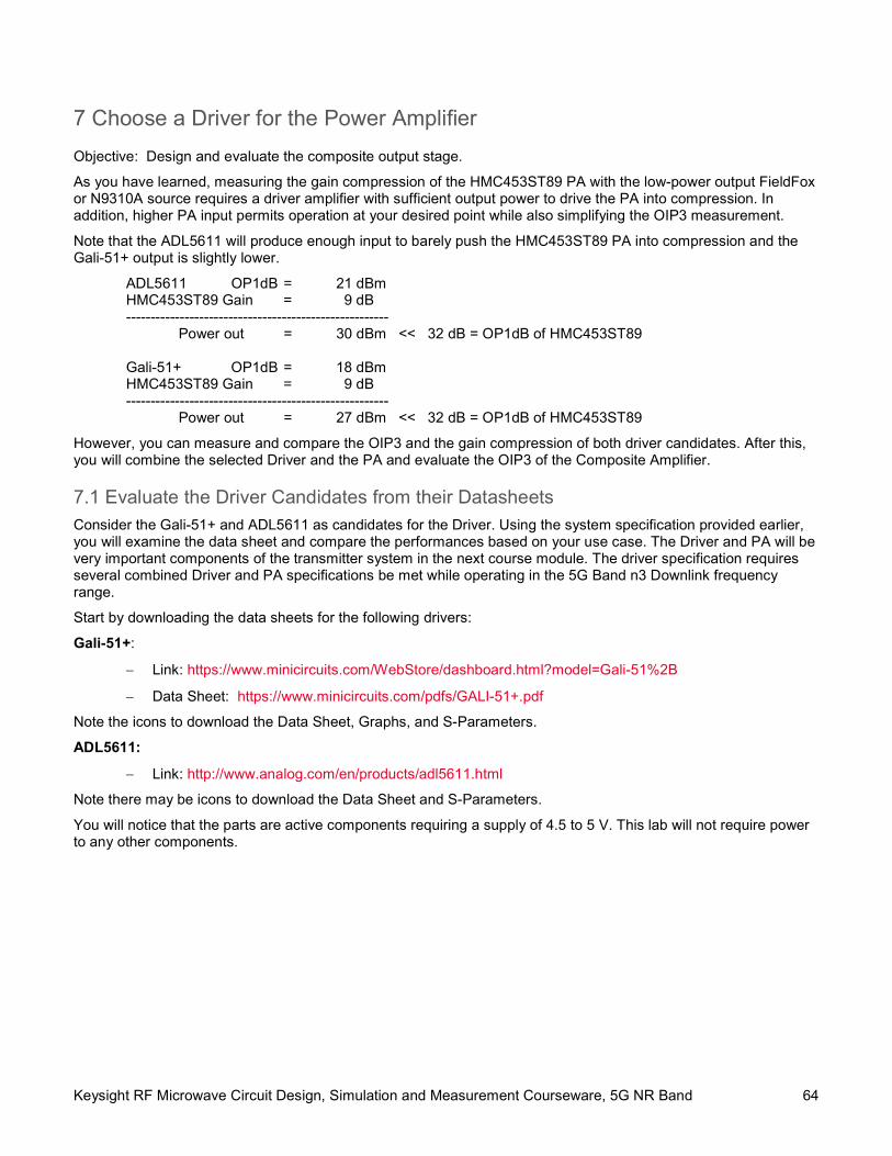
Keysight RF Microwave Circuit Design, Simulation and Measurement Courseware, 5G NR Band 64
7 Choose a Driver for the Power Amplifier
Objective: Design and evaluate the composite output stage.
As you have learned, measuring the gain compression of the HMC453ST89 PA with the low-power output FieldFox or N9310A source requires a driver amplifier with sufficient output power to drive the PA into compression. In addition, higher PA input permits operation at your desired point while also simplifying the OIP3 measurement.
Note that the ADL5611 will produce enough input to barely push the HMC453ST89 PA into compression and the Gali-51+ output is slightly lower.
ADL5611 OP1dB = 21 dBm HMC453ST89 Gain = 9 dB ------------------------------------------------------
Power out = 30 dBm << 32 dB = OP1dB of HMC453ST89
Gali-51+ OP1dB = 18 dBm HMC453ST89 Gain = 9 dB ------------------------------------------------------
Power out = 27 dBm << 32 dB = OP1dB of HMC453ST89
However, you can measure and compare the OIP3 and the gain compression of both driver candidates. After this, you will combine the selected Driver and the PA and evaluate the OIP3 of the Composite Amplifier.
7.1 Evaluate the Driver Candidates from their Datasheets Consider the Gali-51+ and ADL5611 as candidates for the Driver. Using the system specification provided earlier, you will examine the data sheet and compare the performances based on your use case. The Driver and PA will be very important components of the transmitter system in the next course module. The driver specification requires several combined Driver and PA specifications be met while operating in the 5G Band n3 Downlink frequency range.
Start by downloading the data sheets for the following drivers:
Gali-51+:
Link: https://www.minicircuits.com/WebStore/dashboard.html?model=Gali-51%2B
Data Sheet: https://www.minicircuits.com/pdfs/GALI-51+.pdf
Note the icons to download the Data Sheet, Graphs, and S-Parameters.
ADL5611:
Link: http://www.analog.com/en/products/adl5611.html
Note there may be icons to download the Data Sheet and S-Parameters.
You will notice that the parts are active components requiring a supply of 4.5 to 5 V. This lab will not require power to any other components.
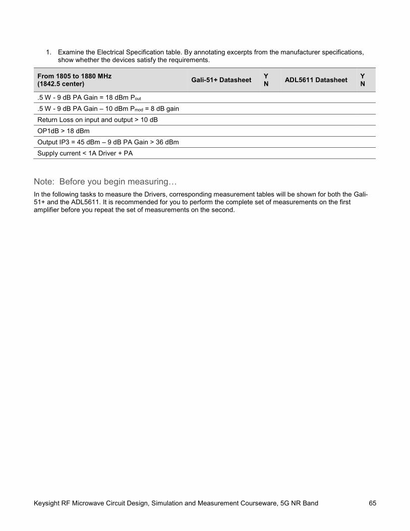
Keysight RF Microwave Circuit Design, Simulation and Measurement Courseware, 5G NR Band 65
1. Examine the Electrical Specification table. By annotating excerpts from the manufacturer specifications, show whether the devices satisfy the requirements.
From 1805 to 1880 MHz (1842.5 center)
Gali-51+ Datasheet Y N
ADL5611 Datasheet Y N
.5 W - 9 dB PA Gain = 18 dBm Pout
.5 W - 9 dB PA Gain – 10 dBm Pmod = 8 dB gain
Return Loss on input and output > 10 dB
OP1dB > 18 dBm
Output IP3 = 45 dBm – 9 dB PA Gain > 36 dBm
Supply current < 1A Driver + PA
Note: Before you begin measuring… In the following tasks to measure the Drivers, corresponding measurement tables will be shown for both the Gali-51+ and the ADL5611. It is recommended for you to perform the complete set of measurements on the first amplifier before you repeat the set of measurements on the second.
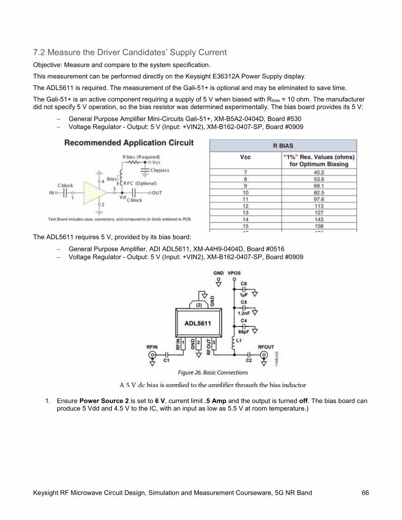
Keysight RF Microwave Circuit Design, Simulation and Measurement Courseware, 5G NR Band 66
7.2 Measure the Driver Candidates’ Supply Current
Objective: Measure and compare to the system specification.
This measurement can be performed directly on the Keysight E36312A Power Supply display.
The ADL5611 is required. The measurement of the Gali-51+ is optional and may be eliminated to save time.
The Gali-51+ is an active component requiring a supply of 5 V when biased with Rbias = 10 ohm. The manufacturer did not specify 5 V operation, so the bias resistor was determined experimentally. The bias board provides its 5 V:
General Purpose Amplifier Mini-Circuits Gali-51+, XM-B5A2-0404D, Board #530 Voltage Regulator - Output: 5 V (Input: +VIN2), XM-B162-0407-SP, Board #0909
The ADL5611 requires 5 V, provided by its bias board:
General Purpose Amplifier, ADI ADL5611, XM-A4H9-0404D, Board #0516 Voltage Regulator - Output: 5 V (Input: +VIN2), XM-B162-0407-SP, Board #0909
1. Ensure Power Source 2 is set to 6 V, current limit .5 Amp and the output is turned off. The bias board can produce 5 Vdd and 4.5 V to the IC, with an input as low as 5.5 V at room temperature.)
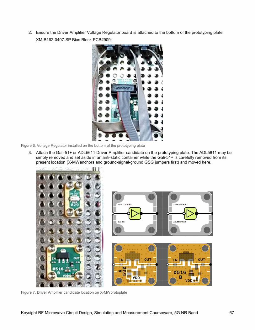
Keysight RF Microwave Circuit Design, Simulation and Measurement Courseware, 5G NR Band 67
2. Ensure the Driver Amplifier Voltage Regulator board is attached to the bottom of the prototyping plate:
XM-B162-0407-SP Bias Block PCB#909:
Figure 6. Voltage Regulator installed on the bottom of the prototyping plate
3. Attach the Gali-51+ or ADL5611 Driver Amplifier candidate on the prototyping plate. The ADL5611 may be simply removed and set aside in an anti-static container while the Gali-51+ is carefully removed from its present location (X-MWanchors and ground-signal-ground GSG jumpers first) and moved here.
Figure 7. Driver Amplifier candidate location on X-MWprotoplate
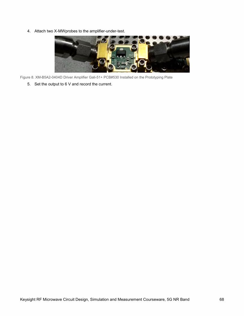
Keysight RF Microwave Circuit Design, Simulation and Measurement Courseware, 5G NR Band 68
4. Attach two X-MWprobes to the amplifier-under-test.
Figure 8. XM-B5A2-0404D Driver Amplifier Gali-51+ PCB#530 Installed on the Prototyping Plate
5. Set the output to 6 V and record the current.
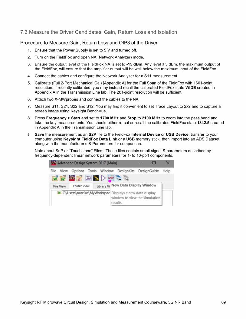
Keysight RF Microwave Circuit Design, Simulation and Measurement Courseware, 5G NR Band 69
7.3 Measure the Driver Candidates’ Gain, Return Loss and Isolation
Procedure to Measure Gain, Return Loss and OIP3 of the Driver
1. Ensure that the Power Supply is set to 5 V and turned off.
2. Turn on the FieldFox and open NA (Network Analyzer) mode.
3. Ensure the output level of the FieldFox NA is set to -15 dBm. Any level ≤ 3 dBm, the maximum output of the FieldFox, will ensure that the amplifier output will be well below the maximum input of the FieldFox.
4. Connect the cables and configure the Network Analyzer for a S11 measurement.
5. Calibrate (Full 2-Port Mechanical Cal) [Appendix A] for the Full Span of the FieldFox with 1601-point resolution. If recently calibrated, you may instead recall the calibrated FieldFox state WIDE created in Appendix A in the Transmission Line lab. The 201-point resolution will be sufficient.
6. Attach two X-MWprobes and connect the cables to the NA.
7. Measure S11, S21, S22 and S12. You may find it convenient to set Trace Layout to 2x2 and to capture a screen image using Keysight BenchVue.
8. Press Frequency > Start and set to 1700 MHz and Stop to 2100 MHz to zoom into the pass band and take the key measurements. You should either re-cal or recall the calibrated FieldFox state 1842.5 created in Appendix A in the Transmission Line lab.
9. Save the measurement as an S2P file to the FieldFox Internal Device or USB Device, transfer to your computer using Keysight FieldFox Data Link or a USB memory stick, then import into an ADS Dataset along with the manufacturer’s S-Parameters for comparison.
Note about SnP or “Touchstone” Files: These files contain small-signal S-parameters described by frequency-dependent linear network parameters for 1- to 10-port components.
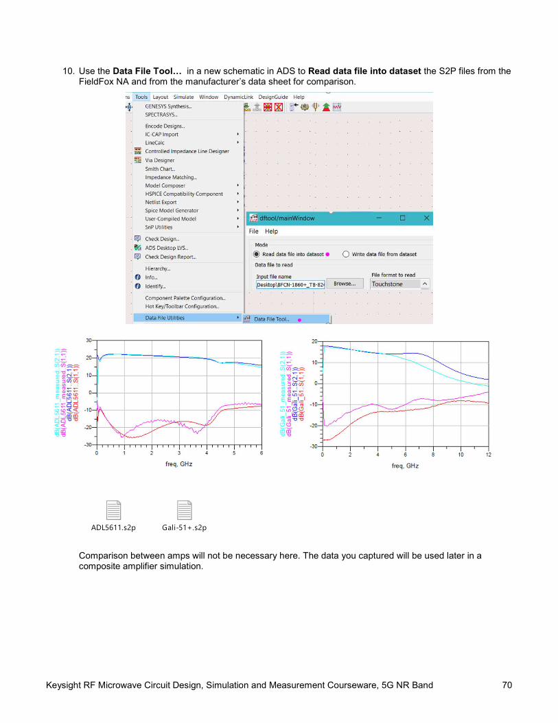
Keysight RF Microwave Circuit Design, Simulation and Measurement Courseware, 5G NR Band 70
10. Use the Data File Tool… in a new schematic in ADS to Read data file into dataset the S2P files from the FieldFox NA and from the manufacturer’s data sheet for comparison.
ADL5611.s2p Gali-51+.s2p
Comparison between amps will not be necessary here. The data you captured will be used later in a composite amplifier simulation.
Keysight RF Microwave Circuit Design, Simulation and Measurement Courseware, 5G NR Band 71
Results: Measured Gain, Return Loss and Isolation
1. Repeat after setting the span from 1700 to 2100 MHz. How do the measurements compare to the data sheets and to each other?
2. You are driving the amplifier input at approximately -15.5 dBm which is 4.5 dB higher than -20 dBm at which the manufacturer graphs describe performance.
Signal Generator = -15 dBm Cable Loss (qty 2) = - .5 dB --------------------------------------------------------- Driver output power = -15.5 dBm
How might this affect the measurement?
3. Try displaying the Smith chart for S11 and S22.
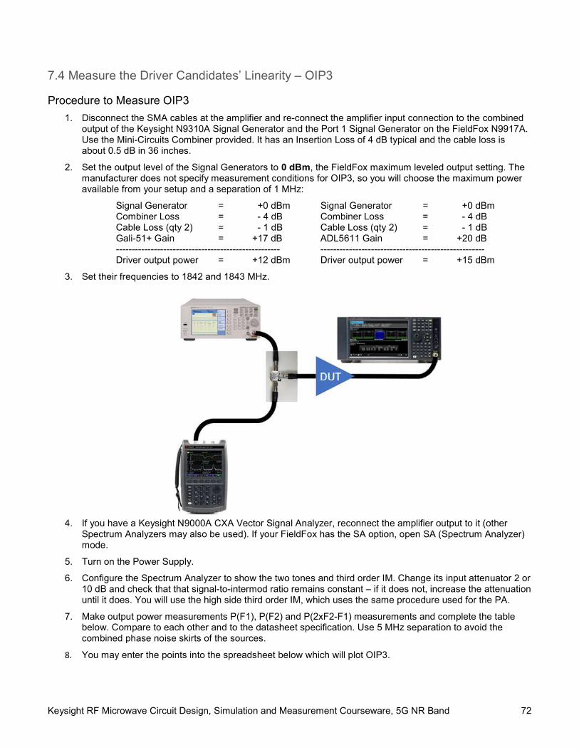
Keysight RF Microwave Circuit Design, Simulation and Measurement Courseware, 5G NR Band 72
7.4 Measure the Driver Candidates’ Linearity – OIP3
Procedure to Measure OIP3
1. Disconnect the SMA cables at the amplifier and re-connect the amplifier input connection to the combined output of the Keysight N9310A Signal Generator and the Port 1 Signal Generator on the FieldFox N9917A. Use the Mini-Circuits Combiner provided. It has an Insertion Loss of 4 dB typical and the cable loss is about 0.5 dB in 36 inches.
2. Set the output level of the Signal Generators to 0 dBm, the FieldFox maximum leveled output setting. The manufacturer does not specify measurement conditions for OIP3, so you will choose the maximum power available from your setup and a separation of 1 MHz:
Signal Generator = +0 dBm Signal Generator = +0 dBm Combiner Loss = - 4 dB Combiner Loss = - 4 dB Cable Loss (qty 2) = - 1 dB Cable Loss (qty 2) = - 1 dB Gali-51+ Gain = +17 dB ADL5611 Gain = +20 dB ---------------------------------------------------- ---------------------------------------------------- Driver output power = +12 dBm Driver output power = +15 dBm
3. Set their frequencies to 1842 and 1843 MHz.
4. If you have a Keysight N9000A CXA Vector Signal Analyzer, reconnect the amplifier output to it (other
Spectrum Analyzers may also be used). If your FieldFox has the SA option, open SA (Spectrum Analyzer) mode.
5. Turn on the Power Supply.
6. Configure the Spectrum Analyzer to show the two tones and third order IM. Change its input attenuator 2 or 10 dB and check that that signal-to-intermod ratio remains constant – if it does not, increase the attenuation until it does. You will use the high side third order IM, which uses the same procedure used for the PA.
7. Make output power measurements P(F1), P(F2) and P(2xF2-F1) measurements and complete the table below. Compare to each other and to the datasheet specification. Use 5 MHz separation to avoid the combined phase noise skirts of the sources.
8. You may enter the points into the spreadsheet below which will plot OIP3.
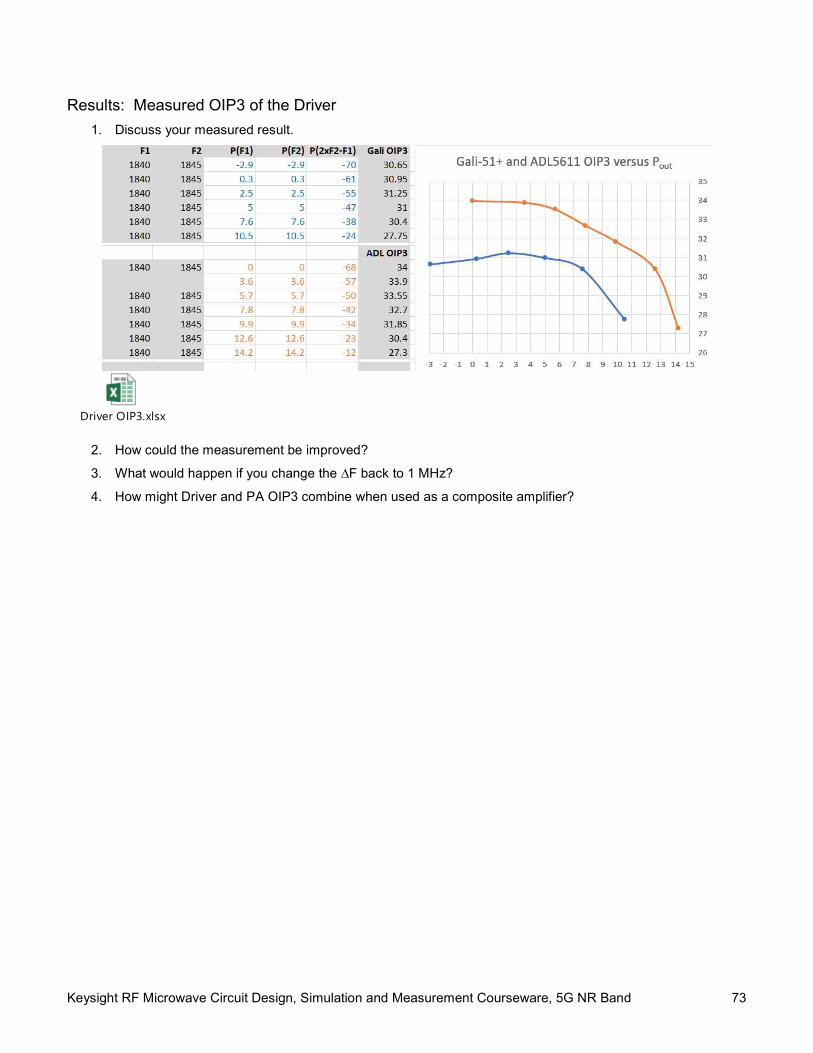
Keysight RF Microwave Circuit Design, Simulation and Measurement Courseware, 5G NR Band 73
Results: Measured OIP3 of the Driver 1. Discuss your measured result.
Driver OIP3.xlsx
2. How could the measurement be improved?
3. What would happen if you change the ∆F back to 1 MHz?
4. How might Driver and PA OIP3 combine when used as a composite amplifier?
Keysight RF Microwave Circuit Design, Simulation and Measurement Courseware, 5G NR Band 74
7.5 Measure the Driver’s Linearity – Gain Compression OP1dB
Procedure to Measure Gain Compression OP1dB
1. Ensure the power supply is set to 6 V and the output is turned off.
2. Disconnect the SMA cables at the amplifier and re-connect the Driver input connection directly to the output of the Keysight N9310A Signal Generator. This connection provides the highest power you can deliver to the amplifier which is necessary to drive it into compression.
3. Set the output level of the Signal Generator to -30 dBm to produce the following amplifier output.
Signal Generator = -30 dBm Signal Generator = -30 dBm Cable Loss (qty 2) = - 1 dB Cable Loss (qty 2) = - 1 dB Gali-51+ Gain = +16 dB ADL5611 Gain = +20 dB ------------------------------------------------------ ------------------------------------------------------ Driver output power = -15 dBm Driver output power = -11 dBm
4. Ensure that the Driver output is cabled to the Spectrum Analyzer and turn on the Power Supply.
5. Configure the Spectrum Analyzer to measure the 1842.5 MHz amplifier output.
6. Measure the output power and repeat for increasing power to fill in the table.
7. Repeat for the second amplifier. Show how you measured the power in the resulting spectrum.
Results: Measured OP1dB
Gali-51+ (Vdd=7 V) (this is provided as reference only since the kit does not provide the ability to bias at 7 V.)
Pin dBm -30 -20 -10 -5 -4 -3 -2 -1 0 1 2 3 4 5 10
PoutDriver’ -15 -5 5 10 11 12 13 14 15 16 17 18 19 20 22
PoutDriver -15 -5 5 10 11 12 13 13.9 14.9 15.8 16.5 17 17.4 17.6 18.4 Gali-51+ (Vdd=5 V)
Pin dBm -30 -20 -10 -5 -4 -3 -2 -1 0 1 2 3 4 5 10
PoutDriver’ -15 -5 5 10 11 12 13 14 15 16 17 18 19 20 22
PoutDriver
ADL5611 Pin dBm -30 -20 -10 -5 -4 -3 -2 -1 0 1 2 3 4 5 10
PoutDriver’ -10 0 10 15 16 17 18 19 20 21 22 23 24 25 30
PoutDriver
Keysight RF Microwave Circuit Design, Simulation and Measurement Courseware, 5G NR Band 75
1. Highlight the 1 dB Gain Compression Point. How does the measurement compare with the data sheet? Can you operate near the Compression Point?
2. Which amplifier should be selected as the driver?
Keysight RF Microwave Circuit Design, Simulation and Measurement Courseware, 5G NR Band 76
Keysight RF Microwave Lab Courseware RF Microwave Circuit Design, Simulation and Measurement Courseware, 5G NR Band Lab 5: Oscillators and Synthesizers
Lab Sheet

Keysight RF Microwave Circuit Design, Simulation and Measurement Courseware, 5G NR Band 77
Notices
Copyright Notice © Keysight Technologies 2019 No part of this manual may be reproduced in any form or by any means (including electronic storage and retrieval or translation into a foreign language) without prior agreement and written consent from Keysight Technologies as governed by United States and international copyright laws.
Edition Edition 1, May 2019
Printed in: Printed in Malaysia
All rights reserved. License terms – see www.keysight.com/find/courseware
Published by: Keysight Technologies Bayan Lepas Free Industrial Zone, 11900 Penang, Malaysia
Technology Licenses The hardware and/or software described in this document are furnished under a license and may be used or copied only in accordance with the terms of such license.
Declaration of Conformity Declarations of Conformity for this product and for other Keysight products may be downloaded from the Web. Go to http://www.keysight.com/go/conformity. You can then search by product number to find the latest Declaration of Conformity.
U.S. Government Rights The Software is “commercial computer software,” as defined by Federal Acquisition Regulation (“FAR”) 2.101. Pursuant to FAR 12.212 and 27.405-3 and Department of Defense FAR Supplement (“DFARS”) 227.7202, the U.S. government acquires commercial computer software under the same terms by which the software is customarily provided to the public. Accordingly, Keysight provides the Software to U.S. government customers under its standard commercial license, which is embodied in its End User License Agreement (EULA), a copy of which can be found at http://www.keysight.com/find/sweula. The license set forth in the EULA represents the exclusive authority by which the U.S. gov-ernment may use, modify, distribute, or dis-close the Software. The EULA and the li-cense set forth therein, does not require or permit, among other things, that Keysight: (1) Furnish technical information related to commercial computer software or com-mercial computer software documentation that is not customarily provided to the public; or (2) Relinquish to, or otherwise provide, the government rights in excess of these rights customarily provided to the public to use, modify, reproduce, release, perform, display, or disclose commercial computer software or commercial computer software documentation. No additional government requirements beyond those set forth in the EULA shall apply, except to the extent that those terms, rights, or licenses are explicitly required from all providers of commercial computer software pursuant to the FAR and the DFARS and are set forth specifically in writing else- where in the EULA. Keysight shall be under no obligation to update, revise or otherwise modify the Software. With respect to any technical data as defined by FAR 2.101, pursuant to FAR 12.211 and 27.404.2 and DFARS 227.7102, the U.S. government acquires no greater than Limited Rights as defined in FAR 27.401 or DFAR 227.7103-5 (c), as applicable in any technical data.
Warranty THE MATERIAL CONTAINED IN THIS DOCUMENT IS PROVIDED “AS IS,” AND IS SUBJECT TO BEING CHANGED, WITHOUT NOTICE, IN FUTURE EDI-TIONS. FURTHER, TO THE MAXIMUM EXTENT PERMITTED BY APPLICABLE LAW, KEYSIGHT DISCLAIMS ALL WAR-RANTIES, EITHER EXPRESS OR IM-PLIED, WITH REGARD TO THIS MANU-AL AND ANY INFORMATION CON-TAINED HEREIN, INCLUD ING BUT NOT LIMITED TO THE IMPLIED WARRANTIES OF MERCHANTABILITY AND FITNESS FOR A PARTICULAR PURPOSE. KEYSIGHT SHALL NOT BE LIABLE FOR ERRORS OR FOR INCIDENTAL OR CONSEQUENTIAL DAMAGES IN CONNECTION WITH THE FURNISHING, USE, OR PERFORMANCE OF THIS DOCUMENT OR OF ANY INFORMATION CON- TAINED HEREIN. SHOULD KEYSIGHT AND THE USER HAVE A SEPARATE WRITTEN AGREEMENT WITH WAR-RANTY TERMS COVERING THE MATE-RIAL IN THIS DOCUMENT THAT CON-FLICT WITH THESE TERMS, THE WAR-RANTY TERMS IN THE SEPARATE AGREEMENT SHALL CONTROL.
Safety Information
CAUTION A CAUTION notice denotes a hazard. It calls attention to an operating procedure, practice, or the like that, if not correctly performed or adhered to, could result in damage to the product or loss of important data. Do not proceed beyond a CAUTION notice until the indicated conditions are fully understood and met.
WARNING A WARNING notice denotes a hazard. It calls attention to an operating procedure, practice, or the like that, if not correctly performed or adhered to, could result in personal injury or death. Do not proceed beyond a WARNING notice until the indicated conditions are fully understood and met.
Keysight RF Microwave Circuit Design, Simulation and Measurement Courseware, 5G NR Band 78
Table of Contents
Notices ........................................................................................................................................................................ 77
Copyright Notice ......................................................................................................................................................... 77 Edition ......................................................................................................................................................................... 77 Printed in: .................................................................................................................................................................... 77 Published by:............................................................................................................................................................... 77 Technology Licenses .................................................................................................................................................. 77 Declaration of Conformity ........................................................................................................................................... 77 U.S. Government Rights ............................................................................................................................................. 77 Warranty ...................................................................................................................................................................... 77 Safety Information ....................................................................................................................................................... 77
Objective ..................................................................................................................................................................... 80
Pre-Lab Setup Instructions .............................................................................................................................................
Equipment Required ....................................................................................................................................................... Accessories Required ..................................................................................................................................................... Suggested Tools ............................................................................................................................................................. Software Required .......................................................................................................................................................... Optional Software ........................................................................................................................................................... Pre-lab Reading .............................................................................................................................................................. References ......................................................................................................................................................................
1 Background ..................................................................................................................................................................
Receiver System Overview .............................................................................................................................................
2 Common Oscillator and Synthesizer Technologies (Physical Attributes) ....................................................................
3 Synthesizer and Oscillator Companies ........................................................................................................................
4 Oscillator and Synthesizer Specifications ....................................................................................................................
5 The Engineer’s Challenge - Oscillator Selection, Simulation and Measurement ........................................................
5.1 Single Mixer Converter Design Example .................................................................................................................. 5.2 LO Design Requirement ...........................................................................................................................................
6 Reference Oscillator Investigation and Measurement Techniques .............................................................................
6.1 Compare the N9310A and SM77D Data Sheets ...................................................................................................... 6.2 Measuring the N9310A at 100 MHz with an Oscilloscope........................................................................................ 6.3 Measuring the N9310A at 100 MHz with Spectrum Analysis ................................................................................... 6.4 Measuring the N9310A at 100 MHz with an SA with Phase Noise Analysis. ........................................................... 6.5 Measuring the SM77D TCXO with Phase Noise Analysis. .......................................................................................
Keysight RF Microwave Circuit Design, Simulation and Measurement Courseware, 5G NR Band 79
Results: Measured Phase Noise ...................................................................................................................................
7 PLL Design, Simulation and Measurement .................................................................................................................
7.1 Reference Oscillator and Synthesizer Design Example using N9310A as a Reference .......................................... 7.2 Reference Oscillator and Synthesizer Design Example using TCXO as a Reference. ............................................
8 Reference Oscillator and Synthesizer Cascade Investigation and Measurement Techniques ............................... 81
8.1 Measuring the Performance of Synthesizer with N9310A as the Reference Oscillator ....................................... 81 8.2 Measuring the Performance of Synthesizer with TCXO as the Reference Oscillator .......................................... 84
Post-Lab Writeup ........................................................................................................................................................ 88
Appendix A - Set up using ADS PLL with Noisy Reference and VCO in PLL Loop ................................................... 89
Keysight RF Microwave Circuit Design, Simulation and Measurement Courseware, 5G NR Band 80
Objective
In this lab, you will learn about RF and microwave oscillators including:
22. Typical heterodyne receiver system block diagram (with focus on the first stage conversion) and the role of the local oscillators (LO)
23. Ideal local oscillator performance versus real world
24. Common oscillator technologies in the Industry (close-up and in production assembly)
25. Oscillator companies and types of oscillators offered
26. Oscillator specifications
27. Synthesizer companies and types of Phase Locked Loops (PLLs) and Voltage Controlled Oscillator (VCOs) offered
28. Synthesizer specifications
29. Importance of phase noise and design techniques to minimize it.
30. The interaction of the reference oscillator, VCO and the PLL loop filter on phase noise
After this information on oscillators, you will use a design specification to design, synthesize, simulate, build, and verify performance:
31. The Engineering Challenge – Decision Tree
32. Steps to design a custom oscillator (2011 MHz PLL with integrated oscillator)
a. Determine specifications from system requirements.
b. Determine the requirements for the reference oscillator.
c. Determine the requirements for the VCO and PLL.
d. Synthesize Loop (ADIsimPLL).
e. Simulate Noise (using ADISimPLL).
f. Prototype / Tune (X-MWblock PLL/VCO on Prototype Station).
g. Measure (CXA).
h. Compare synthesis, simulation, and measurements to specification.
General Flow:
1. Go over phase noise, what it is, and its effects on system performance.
2. Perform first phase noise measurement: Connect N9310A to CXA with phase noise analysis.
3. Use CXA and XMW PLL and measure phase noise.
4. Measure phase noise of reference oscillator.
5. Measure phase noise of entire system.
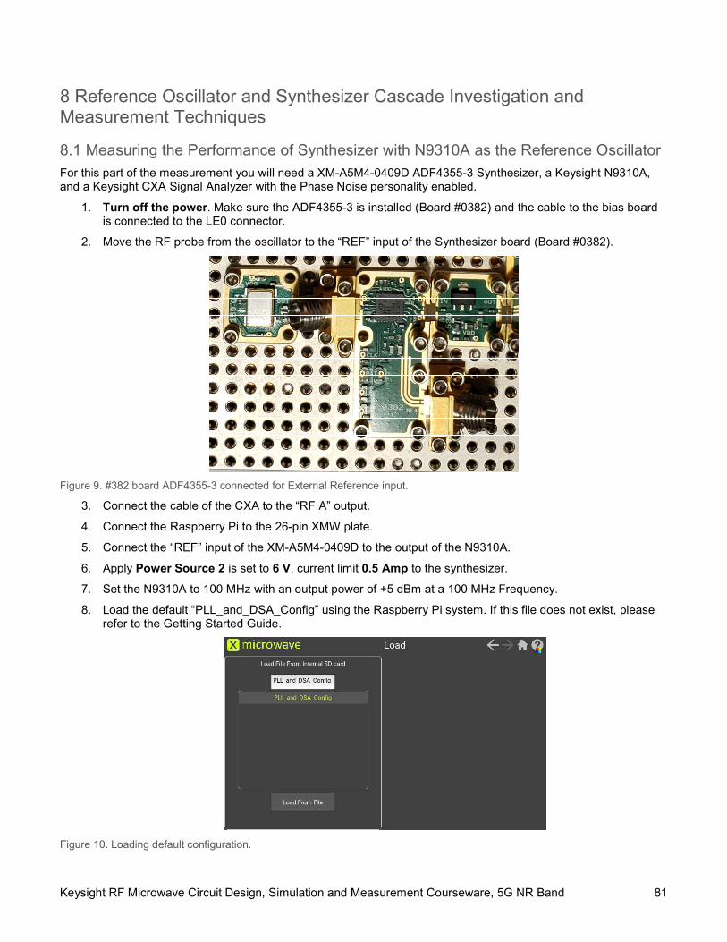
Keysight RF Microwave Circuit Design, Simulation and Measurement Courseware, 5G NR Band 81
8 Reference Oscillator and Synthesizer Cascade Investigation and Measurement Techniques
8.1 Measuring the Performance of Synthesizer with N9310A as the Reference Oscillator
For this part of the measurement you will need a XM-A5M4-0409D ADF4355-3 Synthesizer, a Keysight N9310A, and a Keysight CXA Signal Analyzer with the Phase Noise personality enabled.
1. Turn off the power. Make sure the ADF4355-3 is installed (Board #0382) and the cable to the bias board is connected to the LE0 connector.
2. Move the RF probe from the oscillator to the “REF” input of the Synthesizer board (Board #0382).
Figure 9. #382 board ADF4355-3 connected for External Reference input.
3. Connect the cable of the CXA to the “RF A” output.
4. Connect the Raspberry Pi to the 26-pin XMW plate.
5. Connect the “REF” input of the XM-A5M4-0409D to the output of the N9310A.
6. Apply Power Source 2 is set to 6 V, current limit 0.5 Amp to the synthesizer.
7. Set the N9310A to 100 MHz with an output power of +5 dBm at a 100 MHz Frequency.
8. Load the default “PLL_and_DSA_Config” using the Raspberry Pi system. If this file does not exist, please refer to the Getting Started Guide.
Figure 10. Loading default configuration.
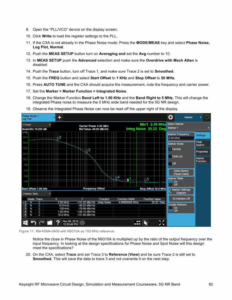
Keysight RF Microwave Circuit Design, Simulation and Measurement Courseware, 5G NR Band 82
9. Open the “PLL/VCO” device on the display screen.
10. Click Write to load the register settings to the PLL.
11. If the CXA is not already in the Phase Noise mode: Press the MODE/MEAS key and select Phase Noise, Log Plot, Normal.
12. Push the MEAS SETUP button turn on Averaging and set the Avg number to 10.
13. In MEAS SETUP push the Advanced selection and make sure the Overdrive with Mech Atten is disabled.
14. Push the Trace button, turn off Trace 1, and make sure Trace 2 is set to Smoothed.
15. Push the FREQ button and select Start Offset to 1 KHz and Stop Offset to 50 MHz.
16. Press AUTO TUNE and the CXA should acquire the measurement, note the frequency and carrier power.
17. Set the Marker > Marker Function > Integrated Noise.
18. Change the Marker Function Band Left to 1.00 KHz and the Band Right to 5 MHz. This will change the integrated Phase noise to measure the 5 MHz wide band needed for the 5G NR design.
19. Observe the Integrated Phase Noise can now be read off the upper right of the display.
Figure 11. XM-A5M4-0409 with N9310A as 100 MHz reference.
Notice the close in Phase Noise of the N9310A is multiplied up by the ratio of the output frequency over the input frequency. In looking at the design specifications for Phase Noise and Spot Noise will this design meet the specifications?
20. On the CXA, select Trace and set Trace 3 to Reference (View) and be sure Trace 2 is still set to Smoothed. This will save the data to trace 3 and not overwrite it on the next step.
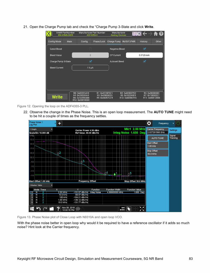
Keysight RF Microwave Circuit Design, Simulation and Measurement Courseware, 5G NR Band 83
21. Open the Charge Pump tab and check the “Charge Pump 3-State and click Write.
Figure 12. Opening the loop on the ADF4355-3 PLL.
22. Observe the change in the Phase Noise. This is an open loop measurement. The AUTO TUNE might need to be hit a couple of times as the frequency settles.
Figure 13. Phase Noise plot of Close Loop with N9310A and open loop VCO.
With the phase noise better in open loop why would it be required to have a reference oscillator if it adds so much noise? Hint look at the Carrier frequency.
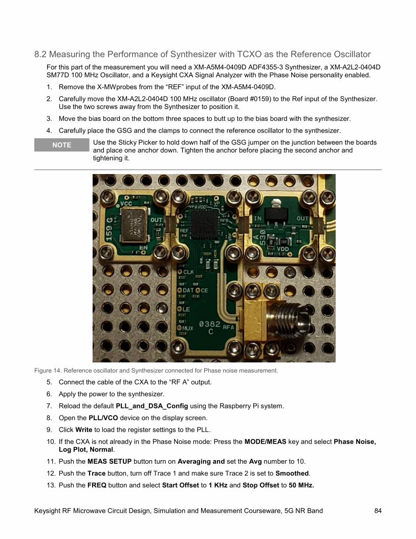
Keysight RF Microwave Circuit Design, Simulation and Measurement Courseware, 5G NR Band 84
8.2 Measuring the Performance of Synthesizer with TCXO as the Reference Oscillator For this part of the measurement you will need a XM-A5M4-0409D ADF4355-3 Synthesizer, a XM-A2L2-0404D SM77D 100 MHz Oscillator, and a Keysight CXA Signal Analyzer with the Phase Noise personality enabled.
1. Remove the X-MWprobes from the “REF” input of the XM-A5M4-0409D.
2. Carefully move the XM-A2L2-0404D 100 MHz oscillator (Board #0159) to the Ref input of the Synthesizer. Use the two screws away from the Synthesizer to position it.
3. Move the bias board on the bottom three spaces to butt up to the bias board with the synthesizer.
4. Carefully place the GSG and the clamps to connect the reference oscillator to the synthesizer.
NOTE Use the Sticky Picker to hold down half of the GSG jumper on the junction between the boards and place one anchor down. Tighten the anchor before placing the second anchor and tightening it.
Figure 14. Reference oscillator and Synthesizer connected for Phase noise measurement.
5. Connect the cable of the CXA to the “RF A” output.
6. Apply the power to the synthesizer.
7. Reload the default PLL_and_DSA_Config using the Raspberry Pi system.
8. Open the PLL/VCO device on the display screen.
9. Click Write to load the register settings to the PLL.
10. If the CXA is not already in the Phase Noise mode: Press the MODE/MEAS key and select Phase Noise, Log Plot, Normal.
11. Push the MEAS SETUP button turn on Averaging and set the Avg number to 10.
12. Push the Trace button, turn off Trace 1 and make sure Trace 2 is set to Smoothed.
13. Push the FREQ button and select Start Offset to 1 KHz and Stop Offset to 50 MHz.
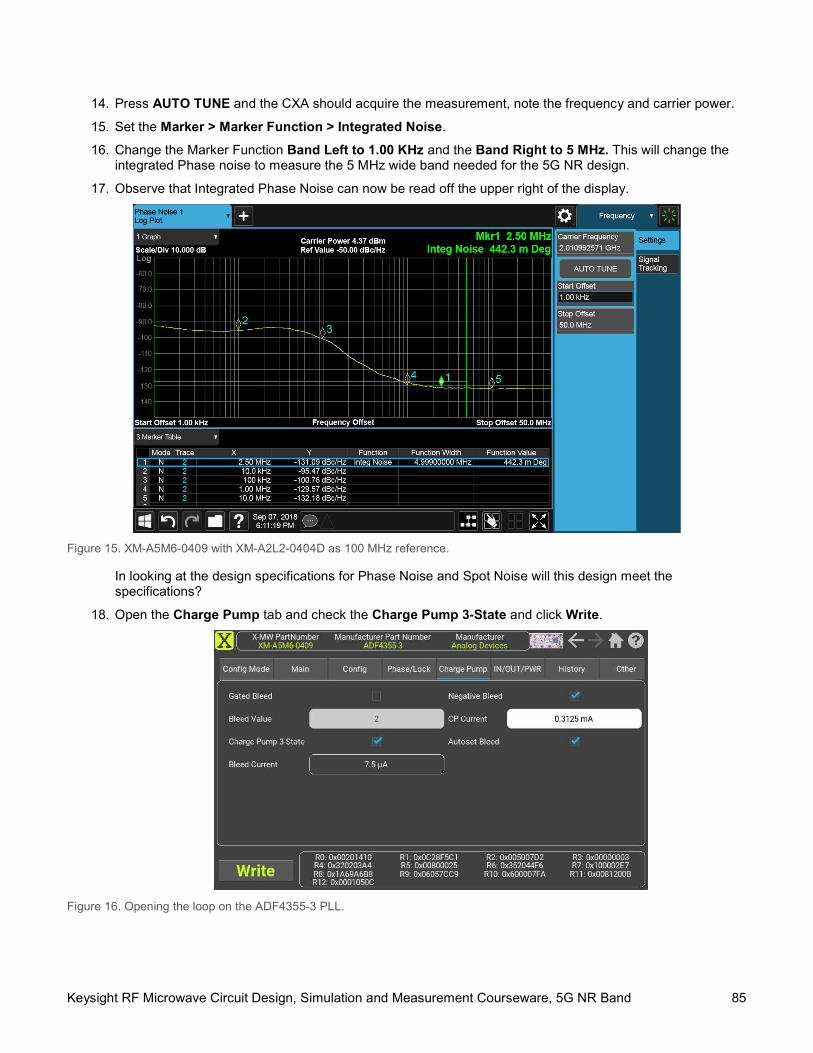
Keysight RF Microwave Circuit Design, Simulation and Measurement Courseware, 5G NR Band 85
14. Press AUTO TUNE and the CXA should acquire the measurement, note the frequency and carrier power.
15. Set the Marker > Marker Function > Integrated Noise.
16. Change the Marker Function Band Left to 1.00 KHz and the Band Right to 5 MHz. This will change the integrated Phase noise to measure the 5 MHz wide band needed for the 5G NR design.
17. Observe that Integrated Phase Noise can now be read off the upper right of the display.
Figure 15. XM-A5M6-0409 with XM-A2L2-0404D as 100 MHz reference.
In looking at the design specifications for Phase Noise and Spot Noise will this design meet the specifications?
18. Open the Charge Pump tab and check the Charge Pump 3-State and click Write.
Figure 16. Opening the loop on the ADF4355-3 PLL.
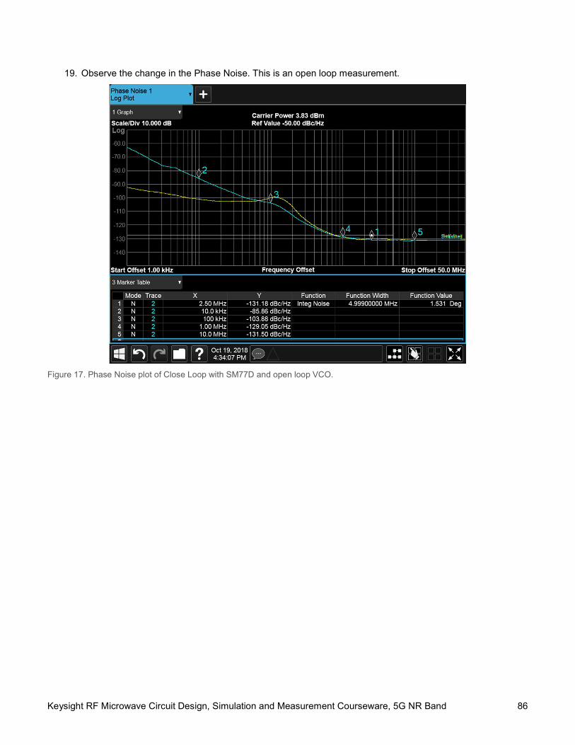
Keysight RF Microwave Circuit Design, Simulation and Measurement Courseware, 5G NR Band 86
19. Observe the change in the Phase Noise. This is an open loop measurement.
Figure 17. Phase Noise plot of Close Loop with SM77D and open loop VCO.
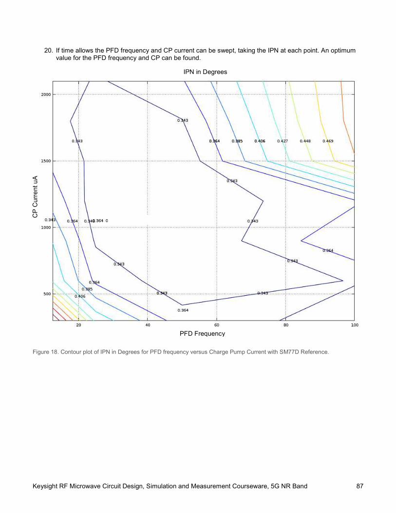
Keysight RF Microwave Circuit Design, Simulation and Measurement Courseware, 5G NR Band 87
20. If time allows the PFD frequency and CP current can be swept, taking the IPN at each point. An optimum value for the PFD frequency and CP can be found.
Figure 18. Contour plot of IPN in Degrees for PFD frequency versus Charge Pump Current with SM77D Reference.
CP
Cu
rre
nt u
A
PFD Frequency
IPN in Degrees
Keysight RF Microwave Circuit Design, Simulation and Measurement Courseware, 5G NR Band 88
Post-Lab Writeup
4. Provide screen captures of all measured data in a single document
5. Label each plot according to the lab step where it was captured.
6. If your results do not match your expectations, explain why.
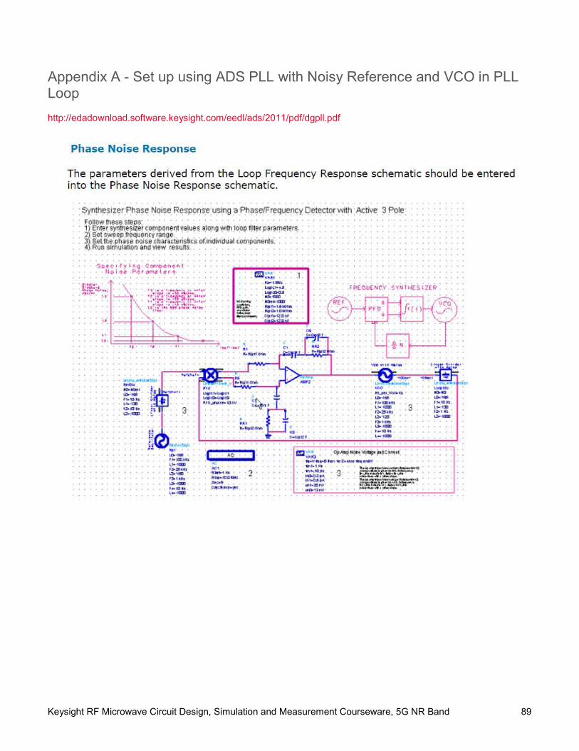
Keysight RF Microwave Circuit Design, Simulation and Measurement Courseware, 5G NR Band 89
Appendix A - Set up using ADS PLL with Noisy Reference and VCO in PLL Loop
http://edadownload.software.keysight.com/eedl/ads/2011/pdf/dgpll.pdf
Page 90
Find us at www.keysight.com
Learn more at: www.keysight.com
For more information on Keysight Technologies’ products, applications or services, please contact your local Keysight office. The complete list is available at: www.keysight.com/find/contactus
This information is subject to change without notice. © Keysight Technologies, 2019, Published in USA, Aug 12, 2019, 5992-3916EN
Keysight RF Microwave Lab Courseware RF Microwave Circuit Design, Simulation and Measurement Courseware, 5G NR Band Lab 6: Mixers
Lab Sheet

Keysight RF Microwave Circuit Design, Simulation and Measurement Courseware, 5G NR Band 91
Notices
Copyright Notice © Keysight Technologies 2019 No part of this manual may be reproduced in any form or by any means (including electronic storage and retrieval or translation into a foreign language) without prior agreement and written consent from Keysight Technologies as governed by United States and international copyright laws.
Edition Edition 1, May 2019
Printed in: Printed in Malaysia
All rights reserved. License terms – see www.keysight.com/find/courseware
Published by: Keysight Technologies Bayan Lepas Free Industrial Zone, 11900 Penang, Malaysia
Technology Licenses The hardware and/or software described in this document are furnished under a license and may be used or copied only in accordance with the terms of such license.
Declaration of Conformity Declarations of Conformity for this product and for other Keysight products may be downloaded from the Web. Go to http://www.keysight.com/go/conformity. You can then search by product number to find the latest Declaration of Conformity.
U.S. Government Rights The Software is “commercial computer software,” as defined by Federal Acquisition Regulation (“FAR”) 2.101. Pursuant to FAR 12.212 and 27.405-3 and Department of Defense FAR Supplement (“DFARS”) 227.7202, the U.S. government acquires commercial computer software under the same terms by which the software is customarily provided to the public. Accordingly, Keysight provides the Software to U.S. government customers under its standard commercial license, which is embodied in its End User License Agreement (EULA), a copy of which can be found at http://www.keysight.com/find/sweula. The license set forth in the EULA represents the exclusive authority by which the U.S. gov-ernment may use, modify, distribute, or dis-close the Software. The EULA and the li-cense set forth therein, does not require or permit, among other things, that Keysight: (1) Furnish technical information related to commercial computer software or com-mercial computer software documentation that is not customarily provided to the public; or (2) Relinquish to, or otherwise provide, the government rights in excess of these rights customarily provided to the public to use, modify, reproduce, release, perform, display, or disclose commercial computer software or commercial computer software documentation. No additional government requirements beyond those set forth in the EULA shall apply, except to the extent that those terms, rights, or licenses are explicitly required from all providers of commercial computer software pursuant to the FAR and the DFARS and are set forth specifically in writing else- where in the EULA. Keysight shall be under no obligation to update, revise or otherwise modify the Software. With respect to any technical data as defined by FAR 2.101, pursuant to FAR 12.211 and 27.404.2 and DFARS 227.7102, the U.S. government acquires no greater than Limited Rights as defined in FAR 27.401 or DFAR 227.7103-5 (c), as applicable in any technical data.
Warranty THE MATERIAL CONTAINED IN THIS DOCUMENT IS PROVIDED “AS IS,” AND IS SUBJECT TO BEING CHANGED, WITHOUT NOTICE, IN FUTURE EDI-TIONS. FURTHER, TO THE MAXIMUM EXTENT PERMITTED BY APPLICABLE LAW, KEYSIGHT DISCLAIMS ALL WAR-RANTIES, EITHER EXPRESS OR IM-PLIED, WITH REGARD TO THIS MANU-AL AND ANY INFORMATION CON-TAINED HEREIN, INCLUD ING BUT NOT LIMITED TO THE IMPLIED WARRANTIES OF MERCHANTABILITY AND FITNESS FOR A PARTICULAR PURPOSE. KEYSIGHT SHALL NOT BE LIABLE FOR ERRORS OR FOR INCIDENTAL OR CONSEQUENTIAL DAMAGES IN CONNECTION WITH THE FURNISHING, USE, OR PERFORMANCE OF THIS DOCUMENT OR OF ANY INFORMATION CON- TAINED HEREIN. SHOULD KEYSIGHT AND THE USER HAVE A SEPARATE WRITTEN AGREEMENT WITH WAR-RANTY TERMS COVERING THE MATE-RIAL IN THIS DOCUMENT THAT CON-FLICT WITH THESE TERMS, THE WAR-RANTY TERMS IN THE SEPARATE AGREEMENT SHALL CONTROL.
Safety Information
CAUTION A CAUTION notice denotes a hazard. It calls attention to an operating procedure, practice, or the like that, if not correctly performed or adhered to, could result in damage to the product or loss of important data. Do not proceed beyond a CAUTION notice until the indicated conditions are fully understood and met.
WARNING A WARNING notice denotes a hazard. It calls attention to an operating procedure, practice, or the like that, if not correctly performed or adhered to, could result in personal injury or death. Do not proceed beyond a WARNING notice until the indicated conditions are fully understood and met.
Keysight RF Microwave Circuit Design, Simulation and Measurement Courseware, 5G NR Band 92
Table of Contents
Notices ........................................................................................................................................................................ 91
Copyright Notice ......................................................................................................................................................... 91 Edition ......................................................................................................................................................................... 91 Printed in: .................................................................................................................................................................... 91 Published by:............................................................................................................................................................... 91 Technology Licenses .................................................................................................................................................. 91 Declaration of Conformity ........................................................................................................................................... 91 U.S. Government Rights ............................................................................................................................................. 91 Warranty ...................................................................................................................................................................... 91 Safety Information ....................................................................................................................................................... 91
Objective ..................................................................................................................................................................... 94
Pre-Lab Setup Instructions .............................................................................................................................................
Equipment Required ....................................................................................................................................................... Accessories Required ..................................................................................................................................................... Software Required .......................................................................................................................................................... Suggested Tools ............................................................................................................................................................ Pre-study reading and viewing........................................................................................................................................
1 Background: What is a Mixer? .....................................................................................................................................
Study the difference in the output Spectral Content of the Ideal Mixer and the Ideal Summer ...................................... Real World Mixer and Summer Waveforms ...................................................................................................................
2 Common Mixer Technologies ......................................................................................................................................
3 Mixer Companies .........................................................................................................................................................
4 Mixer Specifications .....................................................................................................................................................
5 The Engineer’s Challenge - Mixer Selection, Simulation and Measurement ..............................................................
5.1 Single Mixer Converter Design Example .................................................................................................................. 5.2 Mixer Design Requirement .......................................................................................................................................
6 Harmonic Balanced Simulation ....................................................................................................................................
6.1 Genesys Simulation, Synthesis and Comparing Mixers. .......................................................................................... 6.2 Single Diode Unbalanced Mixer. .............................................................................................................................. 6.3 Dual Diode Single Balanced Mixer. .......................................................................................................................... 6.4 Double Balanced Mixer. ............................................................................................................................................ 6.5 Triple (Double-Double) Balanced Mixer. ...................................................................................................................
Keysight RF Microwave Circuit Design, Simulation and Measurement Courseware, 5G NR Band 93
6.6 Simulating S-Parameters of Mixers using Genesys .................................................................................................
7 Measurement of Mixers ........................................................................................................................................... 95
7.1 Measurement of LO Power and Phase Noise ...................................................................................................... 96 7.2 Measurement of Mini-Circuits ADE-1LH Low Frequency Mixer ........................................................................... 99 7.3 Measurement Marki T3 Triple Balanced Mixer ................................................................................................... 103 7.3.1 Measurement of Phase Noise Combining. ...................................................................................................... 108 7.4 Measurement of Mini-Circuits SIM-63 ...................................................................................................................... 7.4.1 Measurement of SIM-63 S11/VSWR .....................................................................................................................
Post-Lab Writeup ............................................................................................................................................................
Appendix A: Configuring the CXA for Phase Noise Measurements. ..............................................................................
Appendix B: Mixer References ......................................................................................................................................
Keysight RF Microwave Circuit Design, Simulation and Measurement Courseware, 5G NR Band 94
Objective
In this lab you will learn about RF and microwave mixers including:
33. Ideal mixer response versus real world
34. Common mixer technologies in industry (close-up and in production assembly)
35. Mixer companies and types of filters offered
36. Mixer specifications
After this introduction to mixers, you will be use a design specification to develop a frequency plan, simulate, build, and verify performance:
37. The engineering challenge explained
38. Steps to develop a frequency plan
a. Determine specifications from system requirements
b. Prototype (X-MWblock on Prototype Station)
c. Measure (FieldFox and CXA)
d. Compare simulation and measurements to specifications
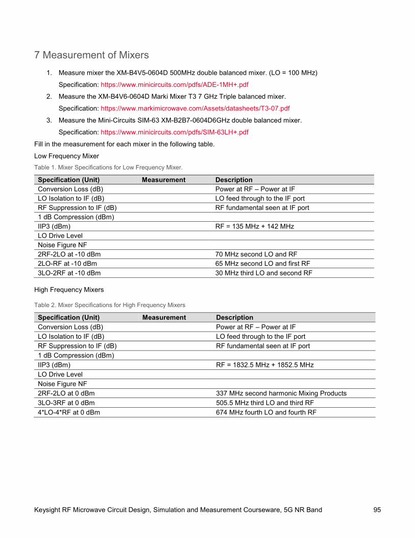
Keysight RF Microwave Circuit Design, Simulation and Measurement Courseware, 5G NR Band 95
7 Measurement of Mixers
1. Measure mixer the XM-B4V5-0604D 500MHz double balanced mixer. (LO = 100 MHz)
Specification: https://www.minicircuits.com/pdfs/ADE-1MH+.pdf
2. Measure the XM-B4V6-0604D Marki Mixer T3 7 GHz Triple balanced mixer.
Specification: https://www.markimicrowave.com/Assets/datasheets/T3-07.pdf
3. Measure the Mini-Circuits SIM-63 XM-B2B7-0604D6GHz double balanced mixer.
Specification: https://www.minicircuits.com/pdfs/SIM-63LH+.pdf
Fill in the measurement for each mixer in the following table.
Low Frequency Mixer
Table 1. Mixer Specifications for Low Frequency Mixer.
Specification (Unit) Measurement Description Conversion Loss (dB) Power at RF – Power at IF LO Isolation to IF (dB) LO feed through to the IF port RF Suppression to IF (dB) RF fundamental seen at IF port 1 dB Compression (dBm) IIP3 (dBm) RF = 135 MHz + 142 MHz LO Drive Level Noise Figure NF 2RF-2LO at -10 dBm 70 MHz second LO and RF 2LO-RF at -10 dBm 65 MHz second LO and first RF
3LO-2RF at -10 dBm 30 MHz third LO and second RF High Frequency Mixers
Table 2. Mixer Specifications for High Frequency Mixers
Specification (Unit) Measurement Description
Conversion Loss (dB) Power at RF – Power at IF
LO Isolation to IF (dB) LO feed through to the IF port
RF Suppression to IF (dB) RF fundamental seen at IF port
1 dB Compression (dBm)
IIP3 (dBm) RF = 1832.5 MHz + 1852.5 MHz
LO Drive Level
Noise Figure NF
2RF-2LO at 0 dBm 337 MHz second harmonic Mixing Products
3LO-3RF at 0 dBm 505.5 MHz third LO and third RF
4*LO-4*RF at 0 dBm 674 MHz fourth LO and fourth RF
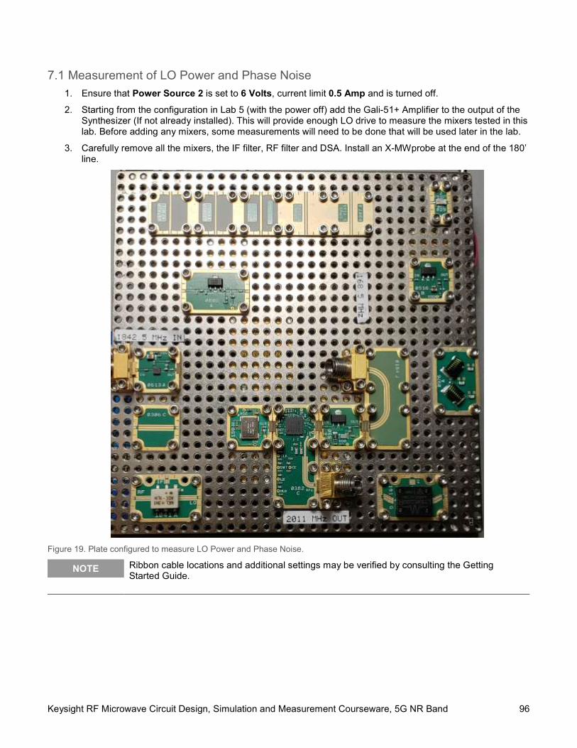
Keysight RF Microwave Circuit Design, Simulation and Measurement Courseware, 5G NR Band 96
7.1 Measurement of LO Power and Phase Noise
1. Ensure that Power Source 2 is set to 6 Volts, current limit 0.5 Amp and is turned off.
2. Starting from the configuration in Lab 5 (with the power off) add the Gali-51+ Amplifier to the output of the Synthesizer (If not already installed). This will provide enough LO drive to measure the mixers tested in this lab. Before adding any mixers, some measurements will need to be done that will be used later in the lab.
3. Carefully remove all the mixers, the IF filter, RF filter and DSA. Install an X-MWprobe at the end of the 180’ line.
Figure 19. Plate configured to measure LO Power and Phase Noise.
NOTE Ribbon cable locations and additional settings may be verified by consulting the Getting Started Guide.
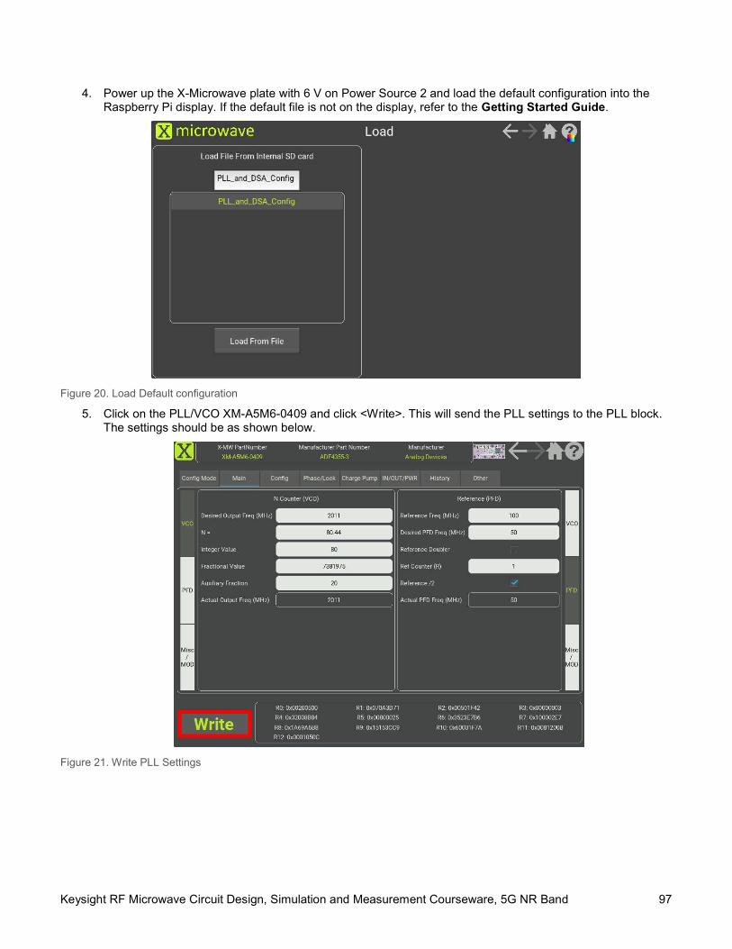
Keysight RF Microwave Circuit Design, Simulation and Measurement Courseware, 5G NR Band 97
4. Power up the X-Microwave plate with 6 V on Power Source 2 and load the default configuration into the Raspberry Pi display. If the default file is not on the display, refer to the Getting Started Guide.
Figure 20. Load Default configuration
5. Click on the PLL/VCO XM-A5M6-0409 and click <Write>. This will send the PLL settings to the PLL block. The settings should be as shown below.
Figure 21. Write PLL Settings
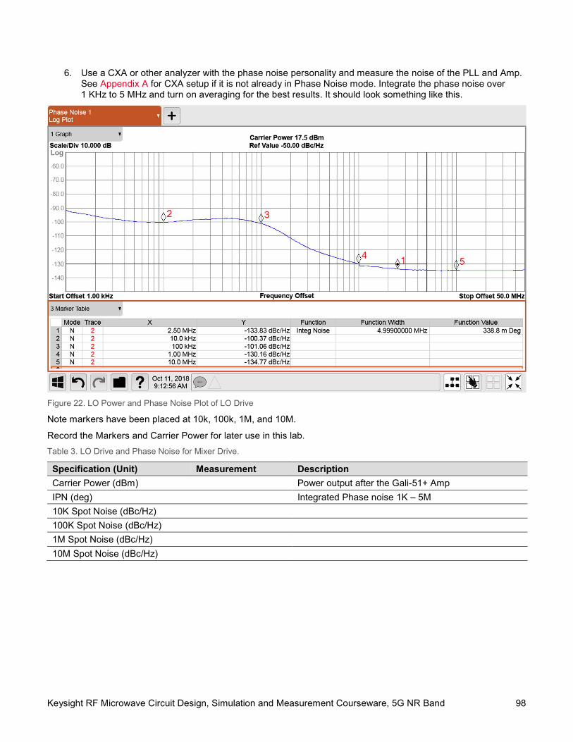
Keysight RF Microwave Circuit Design, Simulation and Measurement Courseware, 5G NR Band 98
6. Use a CXA or other analyzer with the phase noise personality and measure the noise of the PLL and Amp. See Appendix A for CXA setup if it is not already in Phase Noise mode. Integrate the phase noise over 1 KHz to 5 MHz and turn on averaging for the best results. It should look something like this.
Figure 22. LO Power and Phase Noise Plot of LO Drive
Note markers have been placed at 10k, 100k, 1M, and 10M.
Record the Markers and Carrier Power for later use in this lab.
Table 3. LO Drive and Phase Noise for Mixer Drive.
Specification (Unit) Measurement Description
Carrier Power (dBm) Power output after the Gali-51+ Amp
IPN (deg) Integrated Phase noise 1K – 5M
10K Spot Noise (dBc/Hz)
100K Spot Noise (dBc/Hz)
1M Spot Noise (dBc/Hz)
10M Spot Noise (dBc/Hz)
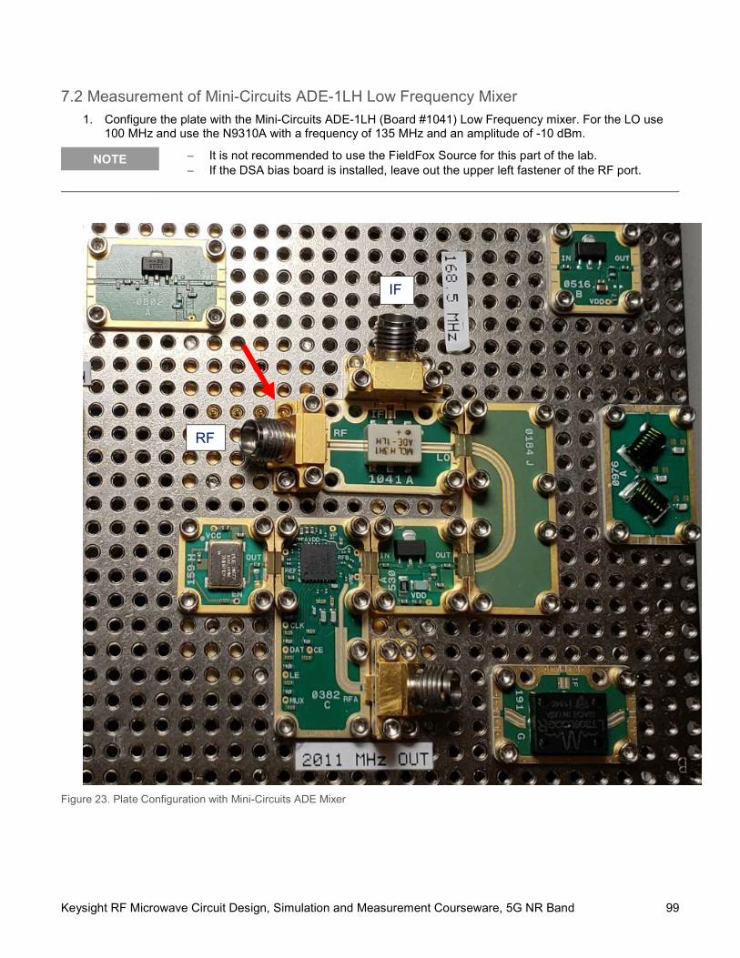
Keysight RF Microwave Circuit Design, Simulation and Measurement Courseware, 5G NR Band 99
7.2 Measurement of Mini-Circuits ADE-1LH Low Frequency Mixer 1. Configure the plate with the Mini-Circuits ADE-1LH (Board #1041) Low Frequency mixer. For the LO use
100 MHz and use the N9310A with a frequency of 135 MHz and an amplitude of -10 dBm.
NOTE It is not recommended to use the FieldFox Source for this part of the lab. If the DSA bias board is installed, leave out the upper left fastener of the RF port.
Figure 23. Plate Configuration with Mini-Circuits ADE Mixer
IF
RF
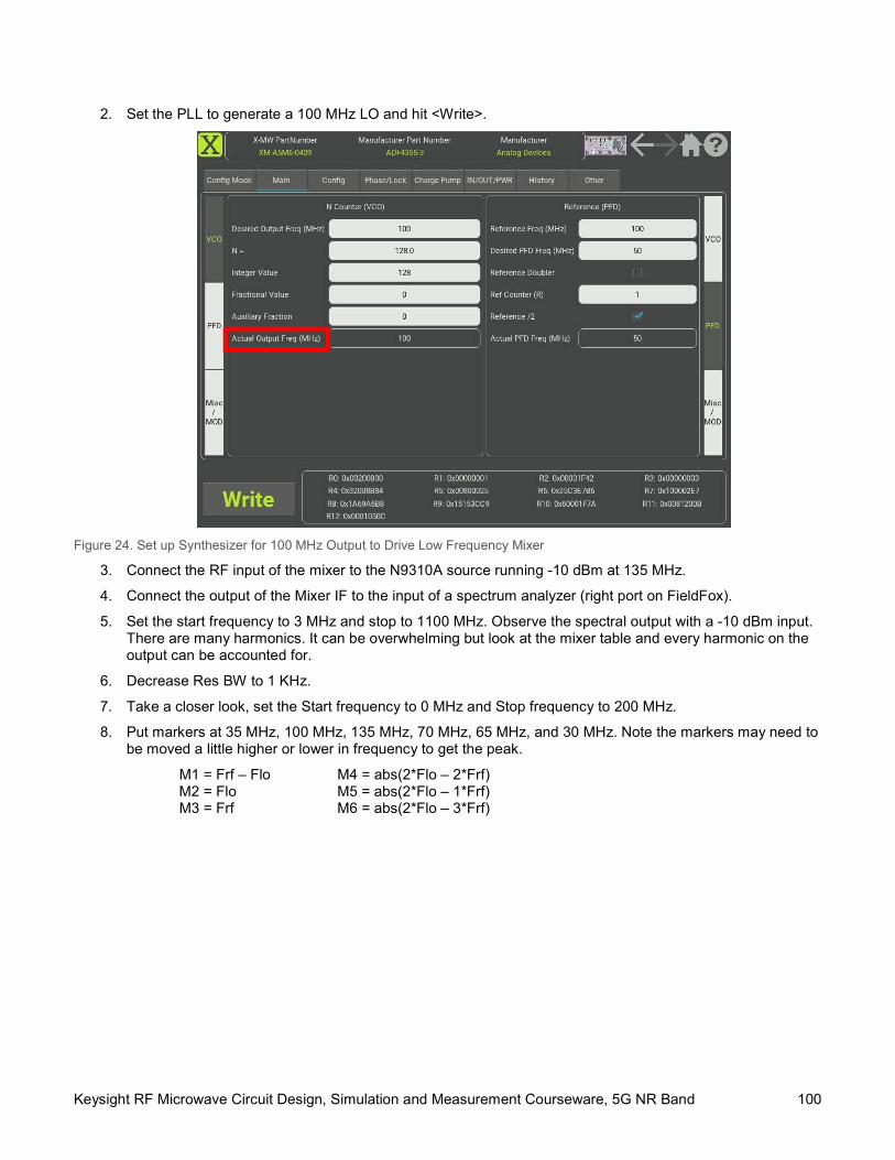
Keysight RF Microwave Circuit Design, Simulation and Measurement Courseware, 5G NR Band 100
2. Set the PLL to generate a 100 MHz LO and hit <Write>.
Figure 24. Set up Synthesizer for 100 MHz Output to Drive Low Frequency Mixer
3. Connect the RF input of the mixer to the N9310A source running -10 dBm at 135 MHz.
4. Connect the output of the Mixer IF to the input of a spectrum analyzer (right port on FieldFox).
5. Set the start frequency to 3 MHz and stop to 1100 MHz. Observe the spectral output with a -10 dBm input. There are many harmonics. It can be overwhelming but look at the mixer table and every harmonic on the output can be accounted for.
6. Decrease Res BW to 1 KHz.
7. Take a closer look, set the Start frequency to 0 MHz and Stop frequency to 200 MHz.
8. Put markers at 35 MHz, 100 MHz, 135 MHz, 70 MHz, 65 MHz, and 30 MHz. Note the markers may need to be moved a little higher or lower in frequency to get the peak.
M1 = Frf – Flo M4 = abs(2*Flo – 2*Frf) M2 = Flo M5 = abs(2*Flo – 1*Frf)
M3 = Frf M6 = abs(2*Flo – 3*Frf)
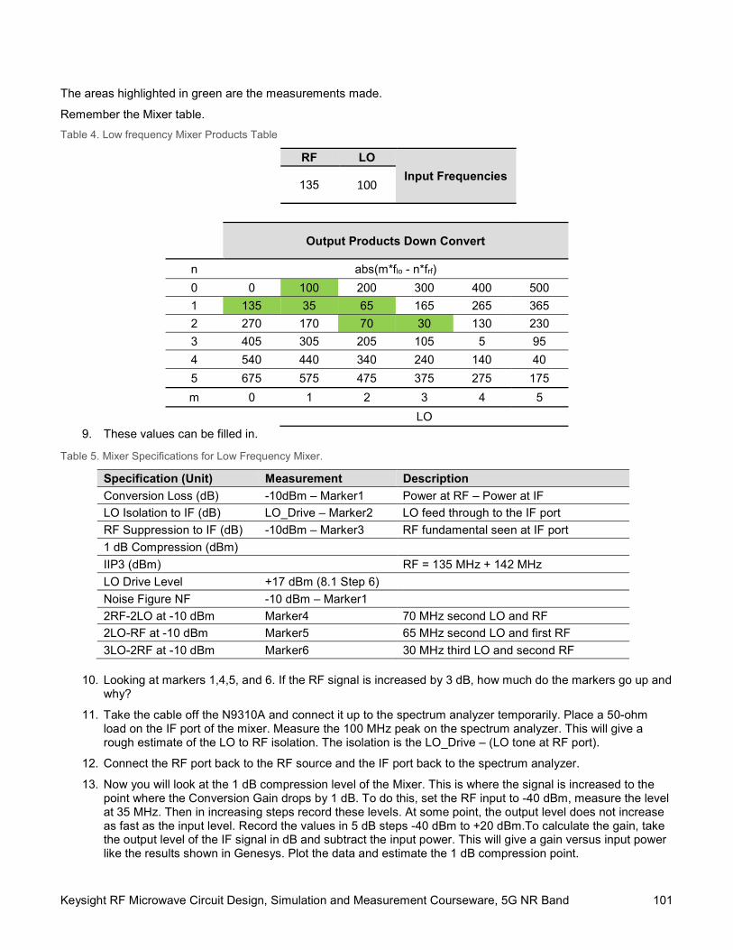
Keysight RF Microwave Circuit Design, Simulation and Measurement Courseware, 5G NR Band 101
The areas highlighted in green are the measurements made.
Remember the Mixer table.
Table 4. Low frequency Mixer Products Table
RF LO
Input Frequencies
135 100
Output Products Down Convert
n abs(m*flo - n*frf)
0 0 100 200 300 400 500
1 135 35 65 165 265 365
2 270 170 70 30 130 230
3 405 305 205 105 5 95
4 540 440 340 240 140 40
5 675 575 475 375 275 175
m 0 1 2 3 4 5 LO
9. These values can be filled in.
Table 5. Mixer Specifications for Low Frequency Mixer.
Specification (Unit) Measurement Description
Conversion Loss (dB) -10dBm – Marker1 Power at RF – Power at IF
LO Isolation to IF (dB) LO_Drive – Marker2 LO feed through to the IF port
RF Suppression to IF (dB) -10dBm – Marker3 RF fundamental seen at IF port
1 dB Compression (dBm)
IIP3 (dBm) RF = 135 MHz + 142 MHz
LO Drive Level +17 dBm (8.1 Step 6)
Noise Figure NF -10 dBm – Marker1
2RF-2LO at -10 dBm Marker4 70 MHz second LO and RF
2LO-RF at -10 dBm Marker5 65 MHz second LO and first RF
3LO-2RF at -10 dBm Marker6 30 MHz third LO and second RF
10. Looking at markers 1,4,5, and 6. If the RF signal is increased by 3 dB, how much do the markers go up and why?
11. Take the cable off the N9310A and connect it up to the spectrum analyzer temporarily. Place a 50-ohm load on the IF port of the mixer. Measure the 100 MHz peak on the spectrum analyzer. This will give a rough estimate of the LO to RF isolation. The isolation is the LO_Drive – (LO tone at RF port).
12. Connect the RF port back to the RF source and the IF port back to the spectrum analyzer.
13. Now you will look at the 1 dB compression level of the Mixer. This is where the signal is increased to the point where the Conversion Gain drops by 1 dB. To do this, set the RF input to -40 dBm, measure the level at 35 MHz. Then in increasing steps record these levels. At some point, the output level does not increase as fast as the input level. Record the values in 5 dB steps -40 dBm to +20 dBm.To calculate the gain, take the output level of the IF signal in dB and subtract the input power. This will give a gain versus input power like the results shown in Genesys. Plot the data and estimate the 1 dB compression point.
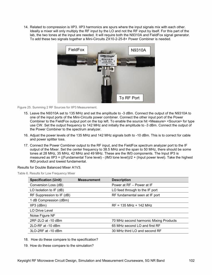
Keysight RF Microwave Circuit Design, Simulation and Measurement Courseware, 5G NR Band 102
14. Related to compression is IIP3. IIP3 harmonics are spurs where the input signals mix with each other. Ideally a mixer will only multiply the RF input by the LO and not the RF input by itself. For this part of the lab, the two tones at the input are needed. It will require both the N9310A and FieldFox signal generator. To add these two signals together a Mini-Circuits ZX10-2-25-8+ Power Combiner is needed.
Figure 25. Summing 2 RF Sources for IIP3 Measurement.
15. Leave the N9310A set to 135 MHz and set the amplitude to -3 dBm. Connect the output of the N9310A to one of the input ports of the Mini-Circuits power combiner. Connect the other input port of the Power Combiner to the FieldFox output port on the top left. To enable the source hit <Measure> <Source> for type use CW. Set the output frequency to 142 MHz and initially the amplitude to -3 dBm. Connect the output of the Power Combiner to the spectrum analyzer.
16. Adjust the power levels of the 135 MHz and 142 MHz signals both to -10 dBm. This is to correct for cable and power splitter loss.
17. Connect the Power Combiner output to the RF input, and the FieldFox spectrum analyzer port to the IF output of the Mixer. Set the center frequency to 38.5 MHz and the span to 50 MHz, there should be some tones at 28 MHz, 35 MHz, 42 MHz and 49 MHz. These are the IM3 components. The Input IP3 is measured as IIP3 = ((Fundamental Tone level) - (IM3 tone level))/2 + (Input power level). Take the highest IM3 product and lowest fundamental.
Results for Double Balanced Mixer A1V3.
Table 6. Results for Low Frequency Mixer
Specification (Unit) Measurement Description
Conversion Loss (dB) Power at RF – Power at IF
LO Isolation to IF (dB) LO feed through to the IF port
RF Suppression to IF (dB) RF fundamental seen at IF port
1 dB Compression (dBm)
IIP3 (dBm) RF = 135 MHz + 142 MHz
LO Drive Level
Noise Figure NF
2RF-2LO at -10 dBm 70 MHz second harmonic Mixing Products
2LO-RF at -10 dBm 65 MHz second LO and first RF
3LO-2RF at -10 dBm 30 MHz third LO and second RF
18. How do these compare to the specification?
19. How do these compare to the simulation?
N9310A FieldFox
To RF Port
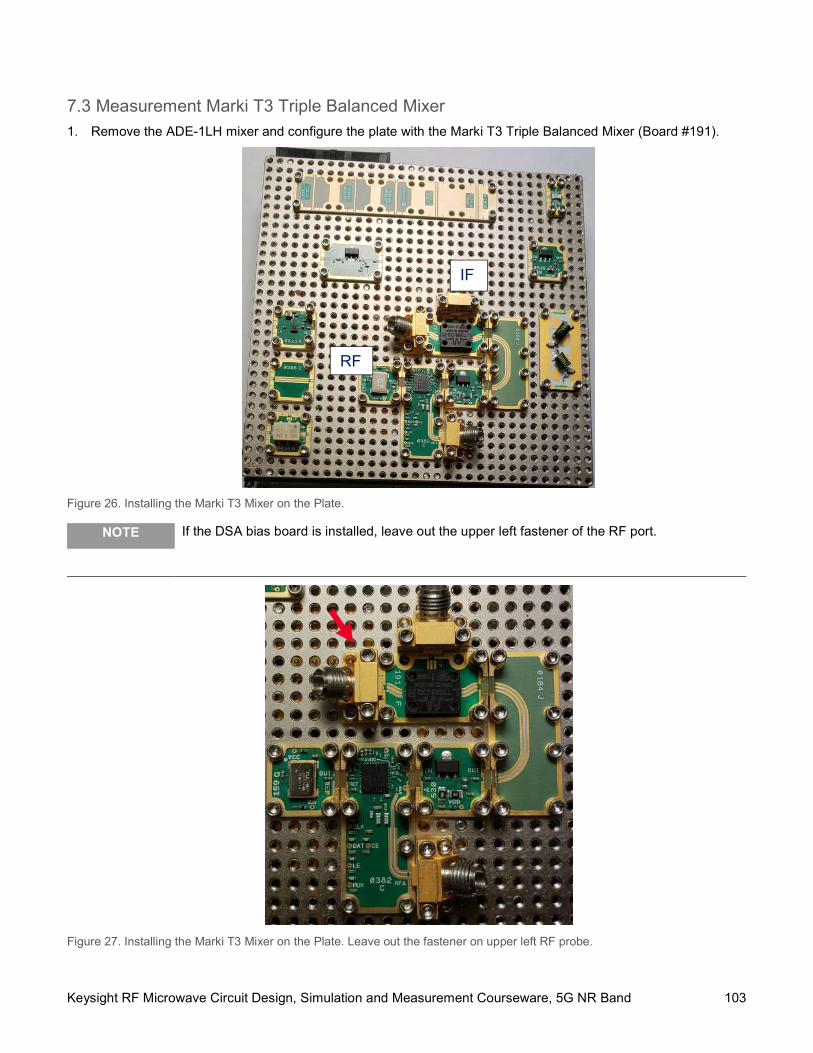
Keysight RF Microwave Circuit Design, Simulation and Measurement Courseware, 5G NR Band 103
7.3 Measurement Marki T3 Triple Balanced Mixer
1. Remove the ADE-1LH mixer and configure the plate with the Marki T3 Triple Balanced Mixer (Board #191).
Figure 26. Installing the Marki T3 Mixer on the Plate.
NOTE If the DSA bias board is installed, leave out the upper left fastener of the RF port.
Figure 27. Installing the Marki T3 Mixer on the Plate. Leave out the fastener on upper left RF probe.
IF
RF
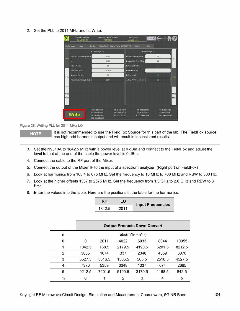
Keysight RF Microwave Circuit Design, Simulation and Measurement Courseware, 5G NR Band 104
2. Set the PLL to 2011 MHz and hit Write.
Figure 28. Writing PLL for 2011 MHz LO
NOTE It is not recommended to use the FieldFox Source for this part of the lab. The FieldFox source has high odd harmonic output and will result in inconsistent results.
3. Set the N9310A to 1842.5 MHz with a power level at 0 dBm and connect to the FieldFox and adjust the level to that at the end of the cable the power level is 0 dBm.
4. Connect the cable to the RF port of the Mixer.
5. Connect the output of the Mixer IF to the input of a spectrum analyzer. (Right port on FieldFox)
6. Look at harmonics from 168.4 to 675 MHz. Set the frequency to 10 MHz to 700 MHz and RBW to 300 Hz.
7. Look at the higher offsets 1337 to 2575 MHz. Set the frequency from 1.3 GHz to 2.6 GHz and RBW to 3 KHz.
8. Enter the values into the table. Here are the positions in the table for the harmonics.
RF LO Input Frequencies
1842.5 2011
Output Products Down Convert
n abs(m*flo - n*frf)
0 0 2011 4022 6033 8044 10055
1 1842.5 168.5 2179.5 4190.5 6201.5 8212.5
2 3685 1674 337 2348 4359 6370
3 5527.5 3516.5 1505.5 505.5 2516.5 4527.5
4 7370 5359 3348 1337 674 2685
5 9212.5 7201.5 5190.5 3179.5 1168.5 842.5
m 0 1 2 3 4 5
Keysight RF Microwave Circuit Design, Simulation and Measurement Courseware, 5G NR Band 105
9. Enter the numbers into a table.
Table 7. Spur Frequencies and Spur levels for Marki T3 Mixer
RF n abs(n*flo - m*frf)
0
1
2
3
4
m 0 1 2 3 4 LO
From specification https://www.markimicrowave.com/Assets/datasheets/T3-07.pdf a Spur calculator was generated. Open this calculator and compare the measured data to the specification.
Microsoft Excel Worksheet
Since the original table was for -5 dBm RF, the RF drive filed will need to be updated. Also, enter your measured conversion loss in the Blue field to correct for any extra loss seen. This will adjust the spur calculations accordingly. The IF peak on the output graph should match your IF level at 168.5 MHz.
Table 8. Expected Spur Levels for Marki T3 Mixer
Output Levels
abs(m*flo - n*frf)
0xLO 1xLO 2xLO 3xLO 4xLO 5xLO
0xRF
1xRF
2xRF
3xRF
4xRF
5xRF
The output IF is -6.126 dBm at 168.5 MHz which is the carrier power at the ouput. To calculate the expected spur power at the output of the mixer subtract the spur table entry from the the fundamental output power.
How did the mixer output spurs compair versus the calculated values from the spur table?
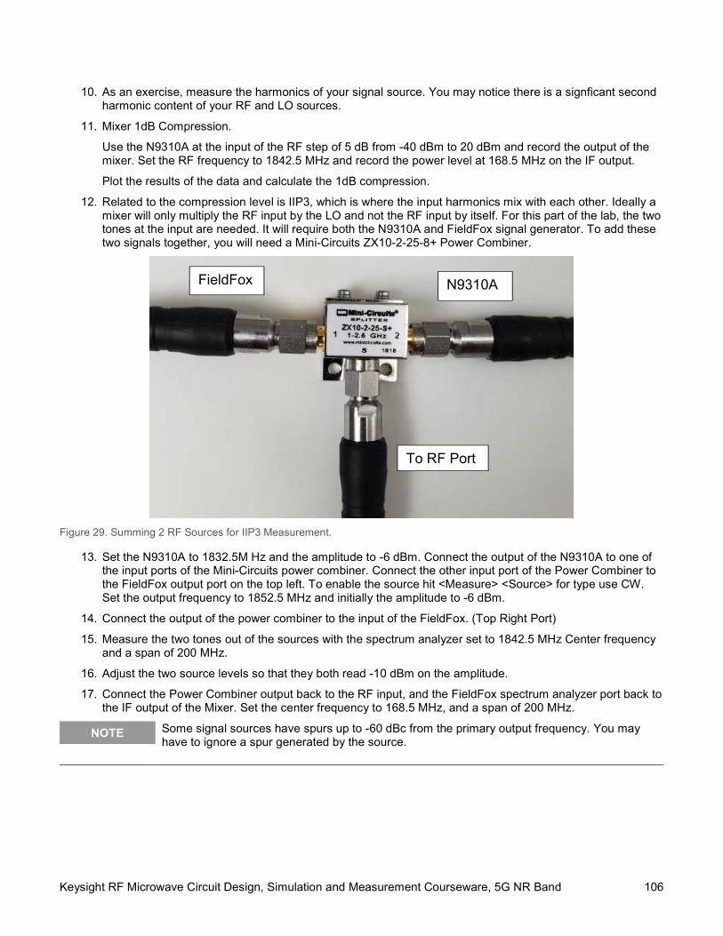
Keysight RF Microwave Circuit Design, Simulation and Measurement Courseware, 5G NR Band 106
10. As an exercise, measure the harmonics of your signal source. You may notice there is a signficant second harmonic content of your RF and LO sources.
11. Mixer 1dB Compression.
Use the N9310A at the input of the RF step of 5 dB from -40 dBm to 20 dBm and record the output of the mixer. Set the RF frequency to 1842.5 MHz and record the power level at 168.5 MHz on the IF output.
Plot the results of the data and calculate the 1dB compression.
12. Related to the compression level is IIP3, which is where the input harmonics mix with each other. Ideally a mixer will only multiply the RF input by the LO and not the RF input by itself. For this part of the lab, the two tones at the input are needed. It will require both the N9310A and FieldFox signal generator. To add these two signals together, you will need a Mini-Circuits ZX10-2-25-8+ Power Combiner.
Figure 29. Summing 2 RF Sources for IIP3 Measurement.
13. Set the N9310A to 1832.5M Hz and the amplitude to -6 dBm. Connect the output of the N9310A to one of the input ports of the Mini-Circuits power combiner. Connect the other input port of the Power Combiner to the FieldFox output port on the top left. To enable the source hit <Measure> <Source> for type use CW. Set the output frequency to 1852.5 MHz and initially the amplitude to -6 dBm.
14. Connect the output of the power combiner to the input of the FieldFox. (Top Right Port)
15. Measure the two tones out of the sources with the spectrum analyzer set to 1842.5 MHz Center frequency and a span of 200 MHz.
16. Adjust the two source levels so that they both read -10 dBm on the amplitude.
17. Connect the Power Combiner output back to the RF input, and the FieldFox spectrum analyzer port back to the IF output of the Mixer. Set the center frequency to 168.5 MHz, and a span of 200 MHz.
NOTE Some signal sources have spurs up to -60 dBc from the primary output frequency. You may have to ignore a spur generated by the source.
N9310A FieldFox
To RF Port
Keysight RF Microwave Circuit Design, Simulation and Measurement Courseware, 5G NR Band 107
18. There should now be some tones at 158.5 and 178.5 MHz which are the fundamental tones. There should also be two other tones at 138.5 and 198.5 MHz which are the IM3 products. The Input IP3 is measured as IIP3 = ((Fundamental Tone level) - (IM3 tone level))/2 + (Input power level). Take the highest IM3 product and lowest fundamental.
Results for Triple Balanced Mixer
Table 9. Results for the Marki T3 Mixer
Specification (Unit) Measurement Description Conversion Loss (dB) Power at RF – Power at IF LO Isolation to IF (dB) LO feed through to the IF port RF Suppression to IF (dB) RF at RF fundamental seen at IF port 1 dB Compression (dBm) IIP3 (dBm) RF = 1832.5 MHz + 1852.5 MHz LO Drive Level Noise Figure NF 2RF-2LO at 0 dBm 337 MHz second harmonic Mixing Products 3LO-3RF at 0 dBm 505.5 MHz third LO and third RF 4*LO-4*RF at 0 dBm 674 MHz fourth LO and fourth RF
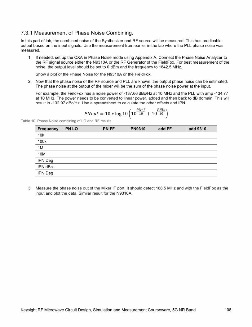
Keysight RF Microwave Circuit Design, Simulation and Measurement Courseware, 5G NR Band 108
7.3.1 Measurement of Phase Noise Combining. In this part of lab, the combined noise of the Synthesizer and RF source will be measured. This has predicable output based on the input signals. Use the measurement from earlier in the lab where the PLL phase noise was measured.
1. If needed, set up the CXA in Phase Noise mode using Appendix A. Connect the Phase Noise Analyzer to the RF signal source either the N9310A or the RF Generator of the FieldFox. For best measurement of the noise, the output level should be set to 0 dBm and the frequency to 1842.5 MHz.
Show a plot of the Phase Noise for the N9310A or the FieldFox.
2. Now that the phase noise of the RF source and PLL are known, the output phase noise can be estimated. The phase noise at the output of the mixer will be the sum of the phase noise power at the input.
For example, the FieldFox has a noise power of -137.66 dBc/Hz at 10 MHz and the PLL with amp -134.77 at 10 MHz. The power needs to be converted to linear power, added and then back to dB domain. This will result in -132.97 dBc/Hz. Use a spreadsheet to calculate the other offsets and IPN.
𝑃𝑁𝑜𝑢𝑡 = 10 ∗ log 10 10 + 10
Table 10. Phase Noise combining of LO and RF results
Frequency PN LO PN FF PN9310 add FF add 9310
10k
100k
1M
10M
IPN Deg
IPN dBc
IPN Deg
3. Measure the phase noise out of the Mixer IF port. It should detect 168.5 MHz and with the FieldFox as the input and plot the data. Similar result for the N9310A.
Keysight RF Microwave Circuit Design, Simulation and Measurement Courseware, 5G NR Band 109
Keysight RF Microwave Lab
Courseware RF Microwave Circuit Design, Simulation and Measurement Courseware, 5G NR Band Lab 7: 5G Receiver Design, Simulation and Measurement
Lab Sheet

Keysight RF Microwave Circuit Design, Simulation and Measurement Courseware, 5G NR Band 110
Notices
Copyright Notice © Keysight Technologies 2019 No part of this manual may be reproduced in any form or by any means (including electronic storage and retrieval or translation into a foreign language) without prior agreement and written consent from Keysight Technologies as governed by United States and international copyright laws.
Edition Edition 1, May 2019
Printed in: Printed in Malaysia
All rights reserved. License terms – see www.keysight.com/find/courseware
Published by: Keysight Technologies Bayan Lepas Free Industrial Zone, 11900 Penang, Malaysia
Technology Licenses The hardware and/or software described in this document are furnished under a license and may be used or copied only in accordance with the terms of such license.
Declaration of Conformity Declarations of Conformity for this product and for other Keysight products may be downloaded from the Web. Go to http://www.keysight.com/go/conformity. You can then search by product number to find the latest Declaration of Conformity.
U.S. Government Rights The Software is “commercial computer software,” as defined by Federal Acquisition Regulation (“FAR”) 2.101. Pursuant to FAR 12.212 and 27.405-3 and Department of Defense FAR Supplement (“DFARS”) 227.7202, the U.S. government acquires commercial computer software under the same terms by which the software is customarily provided to the public. Accordingly, Keysight provides the Software to U.S. government customers under its standard commercial license, which is embodied in its End User License Agreement (EULA), a copy of which can be found at http://www.keysight.com/find/sweula. The license set forth in the EULA represents the exclusive authority by which the U.S. gov-ernment may use, modify, distribute, or dis-close the Software. The EULA and the li-cense set forth therein, does not require or permit, among other things, that Keysight: (1) Furnish technical information related to commercial computer software or com-mercial computer software documentation that is not customarily provided to the public; or (2) Relinquish to, or otherwise provide, the government rights in excess of these rights customarily provided to the public to use, modify, reproduce, release, perform, display, or disclose commercial computer software or commercial computer software documentation. No additional government requirements beyond those set forth in the EULA shall apply, except to the extent that those terms, rights, or licenses are explicitly required from all providers of commercial computer software pursuant to the FAR and the DFARS and are set forth specifically in writing else- where in the EULA. Keysight shall be under no obligation to update, revise or otherwise modify the Software. With respect to any technical data as defined by FAR 2.101, pursuant to FAR 12.211 and 27.404.2 and DFARS 227.7102, the U.S. government acquires no greater than Limited Rights as defined in FAR 27.401 or DFAR 227.7103-5 (c), as applicable in any technical data.
Warranty THE MATERIAL CONTAINED IN THIS DOCUMENT IS PROVIDED “AS IS,” AND IS SUBJECT TO BEING CHANGED, WITHOUT NOTICE, IN FUTURE EDI-TIONS. FURTHER, TO THE MAXIMUM EXTENT PERMITTED BY APPLICABLE LAW, KEYSIGHT DISCLAIMS ALL WAR-RANTIES, EITHER EXPRESS OR IM-PLIED, WITH REGARD TO THIS MANU-AL AND ANY INFORMATION CON-TAINED HEREIN, INCLUD ING BUT NOT LIMITED TO THE IMPLIED WARRANTIES OF MERCHANTABILITY AND FITNESS FOR A PARTICULAR PURPOSE. KEYSIGHT SHALL NOT BE LIABLE FOR ERRORS OR FOR INCIDENTAL OR CONSEQUENTIAL DAMAGES IN CONNECTION WITH THE FURNISHING, USE, OR PERFORMANCE OF THIS DOCUMENT OR OF ANY INFORMATION CON- TAINED HEREIN. SHOULD KEYSIGHT AND THE USER HAVE A SEPARATE WRITTEN AGREEMENT WITH WAR-RANTY TERMS COVERING THE MATE-RIAL IN THIS DOCUMENT THAT CON-FLICT WITH THESE TERMS, THE WAR-RANTY TERMS IN THE SEPARATE AGREEMENT SHALL CONTROL.
Safety Information
CAUTION A CAUTION notice denotes a hazard. It calls attention to an operating procedure, practice, or the like that, if not correctly performed or adhered to, could result in damage to the product or loss of important data. Do not proceed beyond a CAUTION notice until the indicated conditions are fully understood and met.
WARNING A WARNING notice denotes a hazard. It calls attention to an operating procedure, practice, or the like that, if not correctly performed or adhered to, could result in personal injury or death. Do not proceed beyond a WARNING notice until the indicated conditions are fully understood and met.
Keysight RF Microwave Circuit Design, Simulation and Measurement Courseware, 5G NR Band 111
Table of Contents
Notices ...................................................................................................................................................................... 110
Copyright Notice ....................................................................................................................................................... 110 Edition ....................................................................................................................................................................... 110 Printed in: .................................................................................................................................................................. 110 Published by:............................................................................................................................................................. 110 Technology Licenses ................................................................................................................................................ 110 Declaration of Conformity ......................................................................................................................................... 110 U.S. Government Rights ........................................................................................................................................... 110 Warranty .................................................................................................................................................................... 110 Safety Information ..................................................................................................................................................... 110
Objective ................................................................................................................................................................... 113
Pre-Lab Setup Instructions .............................................................................................................................................
Equipment Required ....................................................................................................................................................... Accessories Required ..................................................................................................................................................... Software Required .......................................................................................................................................................... Suggested Tools ............................................................................................................................................................ Pre-study reading and viewing........................................................................................................................................
1 Communication System Overview ...............................................................................................................................
Direct Conversion Receiver ............................................................................................................................................ Multi-Conversion Baseband Sampled Receiver ............................................................................................................. Single Conversion Intermediate Frequency (IF) Sampled Receiver ..............................................................................
2 Engineering Design Cycle ............................................................................................................................................
3 Frequency Planning .....................................................................................................................................................
4 RX Converter Synthesis and Simulation ......................................................................................................................
5 Specification Budgeting ...............................................................................................................................................
6 Simulate the Performance of the Single Conversion Receiver....................................................................................
7 Measure the Performance of the Single Conversion Receiver.............................................................................. 114
7.1 Measure the Receiver’s Supply Current ............................................................................................................. 114 7.2 Measure the Receiver’s Gain.............................................................................................................................. 116 7.3 Measure the Receiver’s Spurious Responses .................................................................................................... 117 7.4 Measure the Receiver’s Noise Figure ................................................................................................................. 118 7.5 Measure the Receiver’s OIP3 ............................................................................................................................. 122

Keysight RF Microwave Circuit Design, Simulation and Measurement Courseware, 5G NR Band 112
Results: Measured OIP3 .......................................................................................................................................... 123
Post-Lab Writeup ............................................................................................................................................................
Keysight RF Microwave Circuit Design, Simulation and Measurement Courseware, 5G NR Band 113
Objective
In this lab you will learn about Single Conversion Receivers:
39. Common Receiver Architectures
40. Engineering Design Cycle
41. Frequency Planning (SystemVue)
42. System Level Synthesis Overview
43. Specification Budgeting
44. Steps to design a Single Conversion Receiver
a. Determine Specifications (from system requirements)
b. Simulate (SystemVue)
c. Measure (various instruments)
d. Compare Synthesis, Simulation and Measured results to specification
45. Conclusions from this course
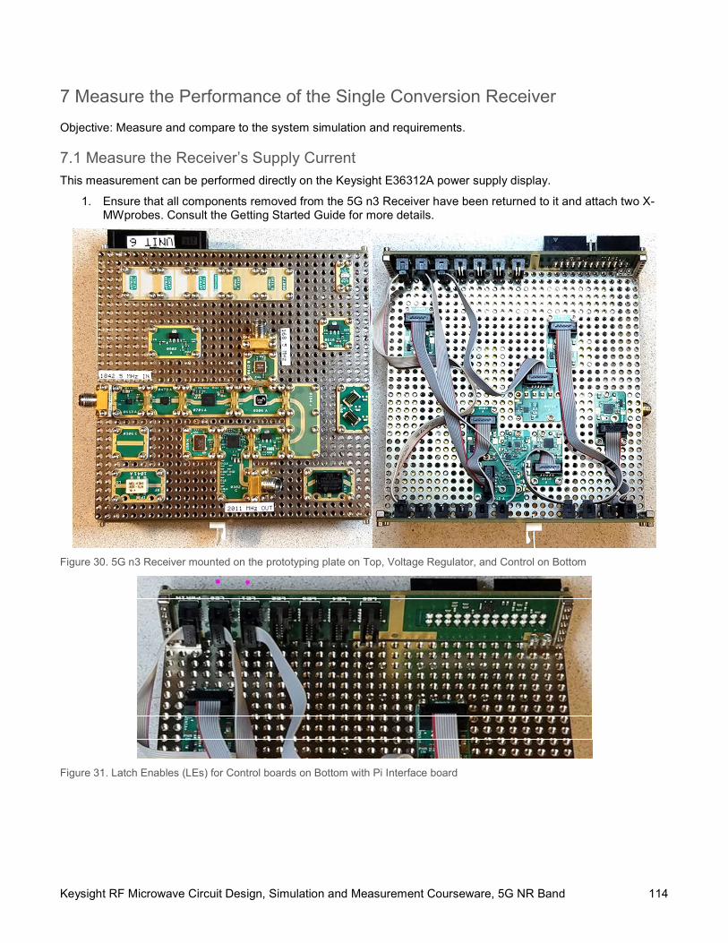
Keysight RF Microwave Circuit Design, Simulation and Measurement Courseware, 5G NR Band 114
7 Measure the Performance of the Single Conversion Receiver
Objective: Measure and compare to the system simulation and requirements.
7.1 Measure the Receiver’s Supply Current This measurement can be performed directly on the Keysight E36312A power supply display.
1. Ensure that all components removed from the 5G n3 Receiver have been returned to it and attach two X-MWprobes. Consult the Getting Started Guide for more details.
Figure 30. 5G n3 Receiver mounted on the prototyping plate on Top, Voltage Regulator, and Control on Bottom
Figure 31. Latch Enables (LEs) for Control boards on Bottom with Pi Interface board
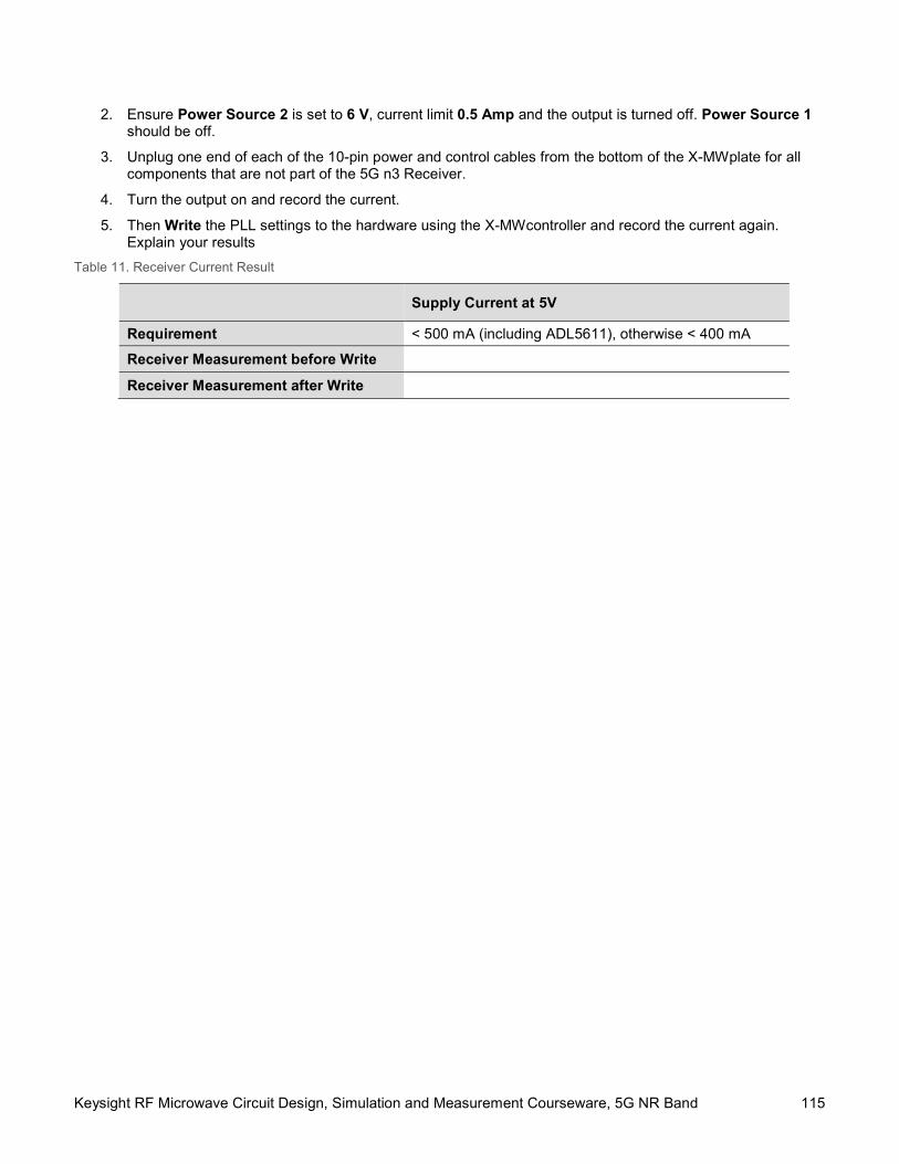
Keysight RF Microwave Circuit Design, Simulation and Measurement Courseware, 5G NR Band 115
2. Ensure Power Source 2 is set to 6 V, current limit 0.5 Amp and the output is turned off. Power Source 1 should be off.
3. Unplug one end of each of the 10-pin power and control cables from the bottom of the X-MWplate for all components that are not part of the 5G n3 Receiver.
4. Turn the output on and record the current.
5. Then Write the PLL settings to the hardware using the X-MWcontroller and record the current again. Explain your results
Table 11. Receiver Current Result
Supply Current at 5V
Requirement < 500 mA (including ADL5611), otherwise < 400 mA
Receiver Measurement before Write
Receiver Measurement after Write
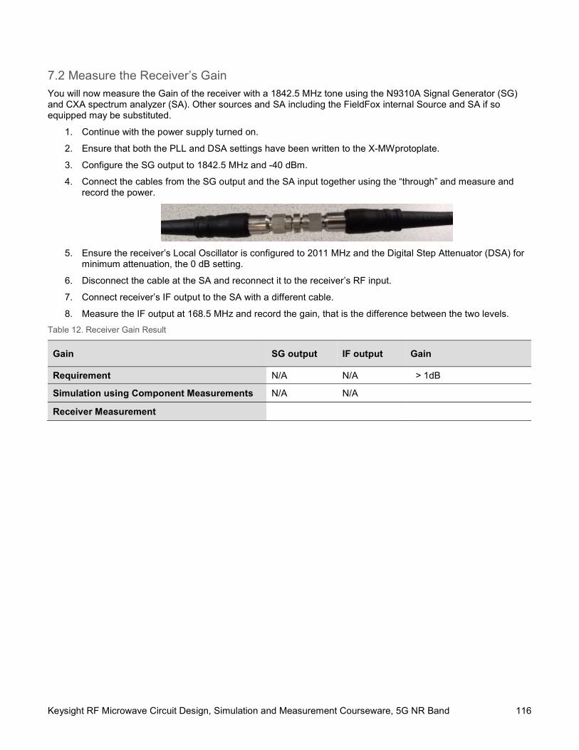
Keysight RF Microwave Circuit Design, Simulation and Measurement Courseware, 5G NR Band 116
7.2 Measure the Receiver’s Gain You will now measure the Gain of the receiver with a 1842.5 MHz tone using the N9310A Signal Generator (SG) and CXA spectrum analyzer (SA). Other sources and SA including the FieldFox internal Source and SA if so equipped may be substituted.
1. Continue with the power supply turned on.
2. Ensure that both the PLL and DSA settings have been written to the X-MWprotoplate.
3. Configure the SG output to 1842.5 MHz and -40 dBm.
4. Connect the cables from the SG output and the SA input together using the “through” and measure and record the power.
5. Ensure the receiver’s Local Oscillator is configured to 2011 MHz and the Digital Step Attenuator (DSA) for
minimum attenuation, the 0 dB setting.
6. Disconnect the cable at the SA and reconnect it to the receiver’s RF input.
7. Connect receiver’s IF output to the SA with a different cable.
8. Measure the IF output at 168.5 MHz and record the gain, that is the difference between the two levels.
Table 12. Receiver Gain Result
Gain SG output IF output Gain
Requirement N/A N/A > 1dB
Simulation using Component Measurements N/A N/A
Receiver Measurement
Keysight RF Microwave Circuit Design, Simulation and Measurement Courseware, 5G NR Band 117
7.3 Measure the Receiver’s Spurious Responses You will now measure the spurious responses of the receiver with the same 1842.5 MHz tone at -40 dBm used above.
1. Continue with the power supply turned on, minimum attenuation and the LO at 2011 MHz.
2. Measure the spurious response at 2 x 168.5 MHz = 337 MHz.
3. Measure the spurious response at 1842.5 MHz (input feedthrough).
4. Measure the spurious response at 2011 MHz (LO feedthrough).
Why are the two feedthrough numbers so different?
Table 13. Receiver Spurious Results
Spurious Responses 337 MHz 1842.5 MHz Input Feedthrough
2011 MHz LO Feedthrough
Requirement < -100 dBm < -100 dBm < -80 dBm
Simulation using Component Measurements
Receiver Measurement of Spurious
Spurious (re-stated) relative to Input or LO
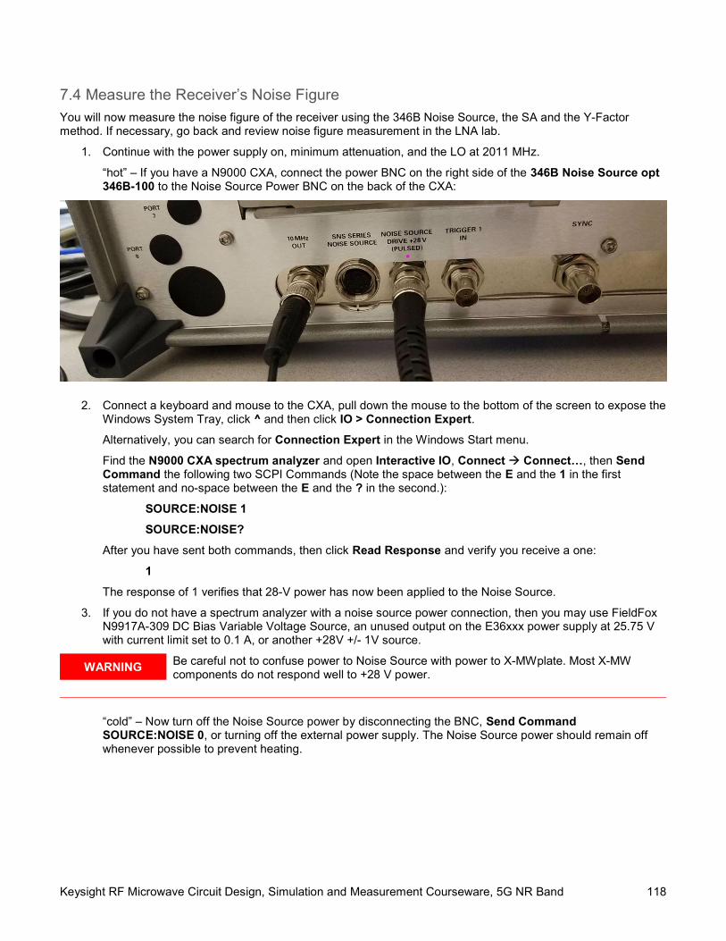
Keysight RF Microwave Circuit Design, Simulation and Measurement Courseware, 5G NR Band 118
7.4 Measure the Receiver’s Noise Figure You will now measure the noise figure of the receiver using the 346B Noise Source, the SA and the Y-Factor method. If necessary, go back and review noise figure measurement in the LNA lab.
1. Continue with the power supply on, minimum attenuation, and the LO at 2011 MHz.
“hot” – If you have a N9000 CXA, connect the power BNC on the right side of the 346B Noise Source opt 346B-100 to the Noise Source Power BNC on the back of the CXA:
2. Connect a keyboard and mouse to the CXA, pull down the mouse to the bottom of the screen to expose the Windows System Tray, click ^ and then click IO > Connection Expert.
Alternatively, you can search for Connection Expert in the Windows Start menu.
Find the N9000 CXA spectrum analyzer and open Interactive IO, Connect Connect…, then Send Command the following two SCPI Commands (Note the space between the E and the 1 in the first statement and no-space between the E and the ? in the second.):
SOURCE:NOISE 1
SOURCE:NOISE?
After you have sent both commands, then click Read Response and verify you receive a one:
1
The response of 1 verifies that 28-V power has now been applied to the Noise Source.
3. If you do not have a spectrum analyzer with a noise source power connection, then you may use FieldFox N9917A-309 DC Bias Variable Voltage Source, an unused output on the E36xxx power supply at 25.75 V with current limit set to 0.1 A, or another +28V +/- 1V source.
WARNING Be careful not to confuse power to Noise Source with power to X-MWplate. Most X-MW components do not respond well to +28 V power.
“cold” – Now turn off the Noise Source power by disconnecting the BNC, Send Command SOURCE:NOISE 0, or turning off the external power supply. The Noise Source power should remain off whenever possible to prevent heating.
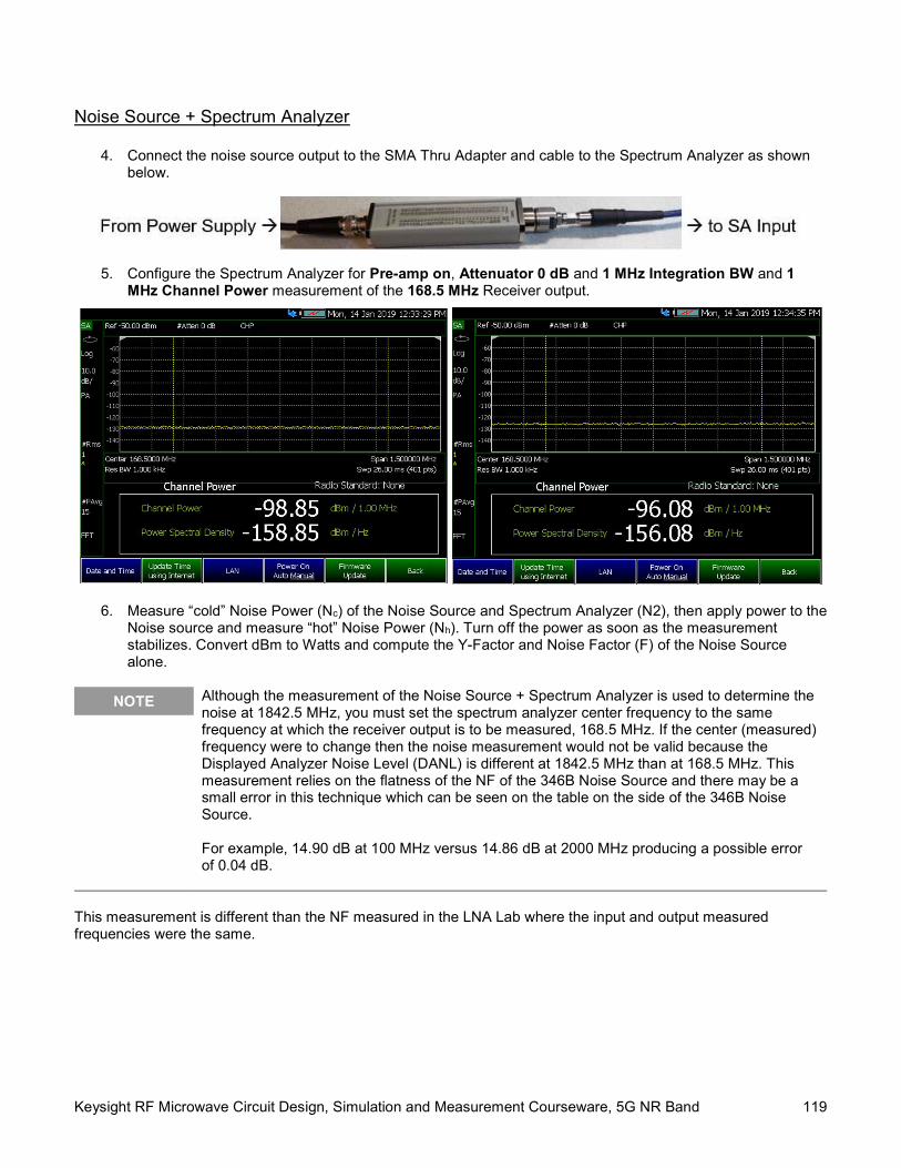
Keysight RF Microwave Circuit Design, Simulation and Measurement Courseware, 5G NR Band 119
Noise Source + Spectrum Analyzer
4. Connect the noise source output to the SMA Thru Adapter and cable to the Spectrum Analyzer as shown below.
5. Configure the Spectrum Analyzer for Pre-amp on, Attenuator 0 dB and 1 MHz Integration BW and 1
MHz Channel Power measurement of the 168.5 MHz Receiver output.
6. Measure “cold” Noise Power (Nc) of the Noise Source and Spectrum Analyzer (N2), then apply power to the Noise source and measure “hot” Noise Power (Nh). Turn off the power as soon as the measurement stabilizes. Convert dBm to Watts and compute the Y-Factor and Noise Factor (F) of the Noise Source alone.
NOTE Although the measurement of the Noise Source + Spectrum Analyzer is used to determine the noise at 1842.5 MHz, you must set the spectrum analyzer center frequency to the same frequency at which the receiver output is to be measured, 168.5 MHz. If the center (measured) frequency were to change then the noise measurement would not be valid because the Displayed Analyzer Noise Level (DANL) is different at 1842.5 MHz than at 168.5 MHz. This measurement relies on the flatness of the NF of the 346B Noise Source and there may be a small error in this technique which can be seen on the table on the side of the 346B Noise Source. For example, 14.90 dB at 100 MHz versus 14.86 dB at 2000 MHz producing a possible error of 0.04 dB.
This measurement is different than the NF measured in the LNA Lab where the input and output measured frequencies were the same.
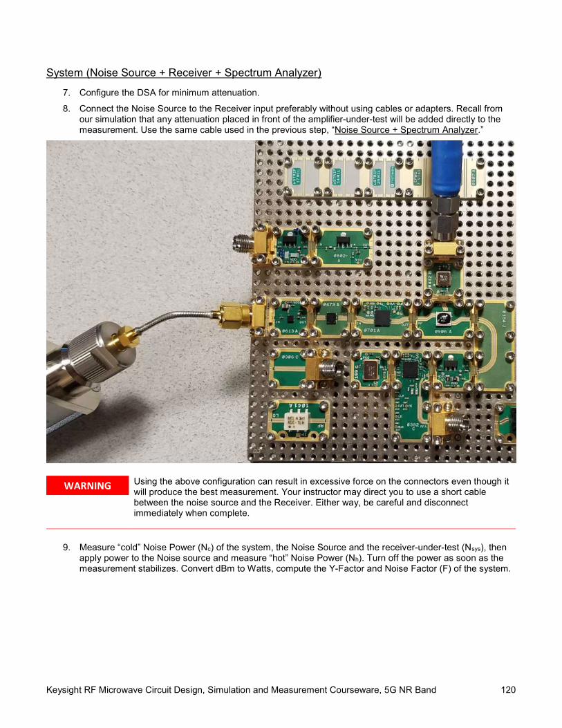
Keysight RF Microwave Circuit Design, Simulation and Measurement Courseware, 5G NR Band 120
System (Noise Source + Receiver + Spectrum Analyzer)
7. Configure the DSA for minimum attenuation.
8. Connect the Noise Source to the Receiver input preferably without using cables or adapters. Recall from our simulation that any attenuation placed in front of the amplifier-under-test will be added directly to the measurement. Use the same cable used in the previous step, “Noise Source + Spectrum Analyzer.”
WARNING Using the above configuration can result in excessive force on the connectors even though it will produce the best measurement. Your instructor may direct you to use a short cable between the noise source and the Receiver. Either way, be careful and disconnect immediately when complete.
9. Measure “cold” Noise Power (Nc) of the system, the Noise Source and the receiver-under-test (Nsys), then
apply power to the Noise source and measure “hot” Noise Power (Nh). Turn off the power as soon as the measurement stabilizes. Convert dBm to Watts, compute the Y-Factor and Noise Factor (F) of the system.
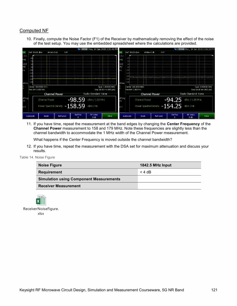
Keysight RF Microwave Circuit Design, Simulation and Measurement Courseware, 5G NR Band 121
Computed NF
10. Finally, compute the Noise Factor (F1) of the Receiver by mathematically removing the effect of the noise of the test setup. You may use the embedded spreadsheet where the calculations are provided.
11. If you have time, repeat the measurement at the band edges by changing the Center Frequency of the Channel Power measurement to 158 and 179 MHz. Note these frequencies are slightly less than the channel bandwidth to accommodate the 1 MHz width of the Channel Power measurement.
What happens if the Center Frequency is moved outside the channel bandwidth?
12. If you have time, repeat the measurement with the DSA set for maximum attenuation and discuss your results.
Table 14. Noise Figure
Noise Figure 1842.5 MHz Input
Requirement < 4 dB
Simulation using Component Measurements
Receiver Measurement
ReceiverNoiseFigure.xlsx
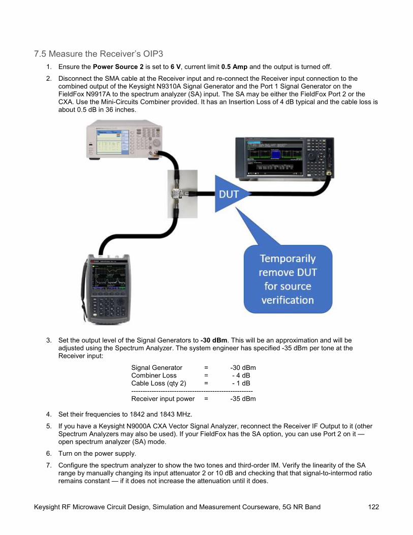
Keysight RF Microwave Circuit Design, Simulation and Measurement Courseware, 5G NR Band 122
7.5 Measure the Receiver’s OIP3
1. Ensure the Power Source 2 is set to 6 V, current limit 0.5 Amp and the output is turned off.
2. Disconnect the SMA cable at the Receiver input and re-connect the Receiver input connection to the combined output of the Keysight N9310A Signal Generator and the Port 1 Signal Generator on the FieldFox N9917A to the spectrum analyzer (SA) input. The SA may be either the FieldFox Port 2 or the CXA. Use the Mini-Circuits Combiner provided. It has an Insertion Loss of 4 dB typical and the cable loss is about 0.5 dB in 36 inches.
3. Set the output level of the Signal Generators to -30 dBm. This will be an approximation and will be adjusted using the Spectrum Analyzer. The system engineer has specified -35 dBm per tone at the Receiver input:
Signal Generator = -30 dBm Combiner Loss = - 4 dB Cable Loss (qty 2) = - 1 dB ------------------------------------------------------ Receiver input power = -35 dBm
4. Set their frequencies to 1842 and 1843 MHz.
5. If you have a Keysight N9000A CXA Vector Signal Analyzer, reconnect the Receiver IF Output to it (other Spectrum Analyzers may also be used). If your FieldFox has the SA option, you can use Port 2 on it — open spectrum analyzer (SA) mode.
6. Turn on the power supply.
7. Configure the spectrum analyzer to show the two tones and third-order IM. Verify the linearity of the SA range by manually changing its input attenuator 2 or 10 dB and checking that that signal-to-intermod ratio remains constant — if it does not increase the attenuation until it does.
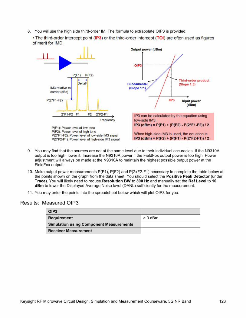
Keysight RF Microwave Circuit Design, Simulation and Measurement Courseware, 5G NR Band 123
8. You will use the high side third-order IM. The formula to extrapolate OIP3 is provided:
9. You may find that the sources are not at the same level due to their individual accuracies. If the N9310A output is too high, lower it. Increase the N9310A power if the FieldFox output power is too high. Power adjustment will always be made at the N9310A to maintain the highest possible output power at the FieldFox output.
10. Make output power measurements P(F1), P(F2) and P(2xF2-F1) necessary to complete the table below at the points shown on the graph from the data sheet. You should select the Positive Peak Detector (under Trace). You will likely need to reduce Resolution BW to 300 Hz and manually set the Ref Level to 10 dBm to lower the Displayed Average Noise level (DANL) sufficiently for the measurement.
11. You may enter the points into the spreadsheet below which will plot OIP3 for you.
Results: Measured OIP3
OIP3
Requirement > 0 dBm
Simulation using Component Measurements
Receiver Measurement

Page 124
Find us at www.keysight.com
Learn more at: www.keysight.com
For more information on Keysight Technologies’ products, applications or services, please contact your local Keysight office. The complete list is available at: www.keysight.com/find/contactus
This information is subject to change without notice. © Keysight Technologies, 2019, Published in USA, Aug 12, 2019, 5992-3916EN
Related Documents