MEMS/NEMS Devices Applications
Micro-electromechanical Systems (MEMS) Nano-electromechanical Systems (NEMS)
The key roles
in many important areas
Chapter 8
MEMS/NEMS Devices
• MEMS are inherently small, thus offering attractive characteristics such as reduced size, weight, and power dissipation and improved speed and precision compared to their macroscopic counterparts.
• A physical displacement of a sensor or an actuator( 驱动器 ) is typically on the same order (等级) of magnitude (数量级) .
• Most MEMS devices exhibit a length or width ranging from micrometers (微米) to several hundreds of micrometers with a thickness from sub-micrometer up to tens of micrometers, depending upon the fabrication(制备) technique employed.
MEMS/NEMS Devices
They have played key roles in many important areas
• transportation,
• communication, • automated manufacturing (制造) , • environmental monitoring, • health care, • defense systems, • and a wide range of consumer products.
MEMS/NEMS Devices
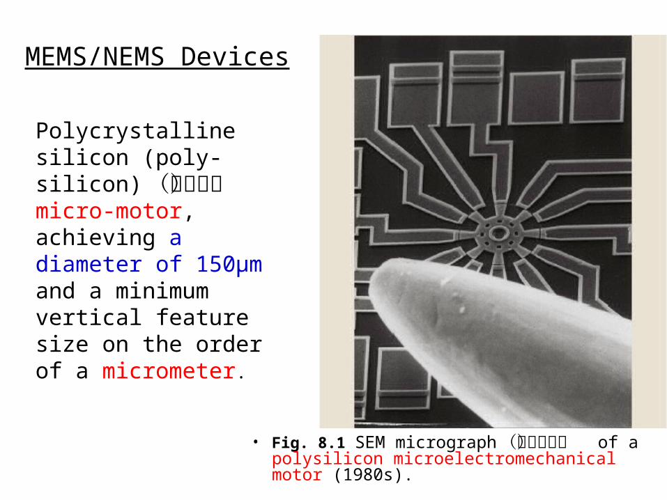
• Fig. 8.1 SEM micrograph (显微照片) of a polysilicon microelectromechanical motor (1980s).
Polycrystalline silicon (poly-silicon) (多晶硅) micro-motor, achieving a diameter of 150μm and a minimum vertical feature size on the order of a micrometer.
MEMS/NEMS Devices
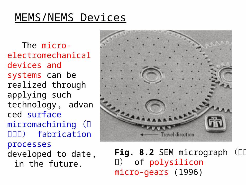
Fig. 8.2 SEM micrograph (显微照片) of polysilicon micro-gears (1996)
The micro-electromechanical devices and systems can be realized through applying such technology , advanced surface micromachining (微细加工) fabrication processes developed to date , in the future.
MEMS/NEMS Devices
Pressure Sensor• Pressure sensors are one of the early devices realized
by silicon micromachining technologies and have become successful commercial products.
• The devices have been widely used in various industrial and biomedical applications.
• Silicon bulk (体硅) and surface micromachining techniques have been used for sensor batch fabrication(成批生产) , thus achieving size miniaturization and low cost.
• Two types of pressure sensors – piezo-resistive (压阻型) and capacitive (电容式)
MEMS/NEMS DevicesPiezo-resistive Pressure Sensor
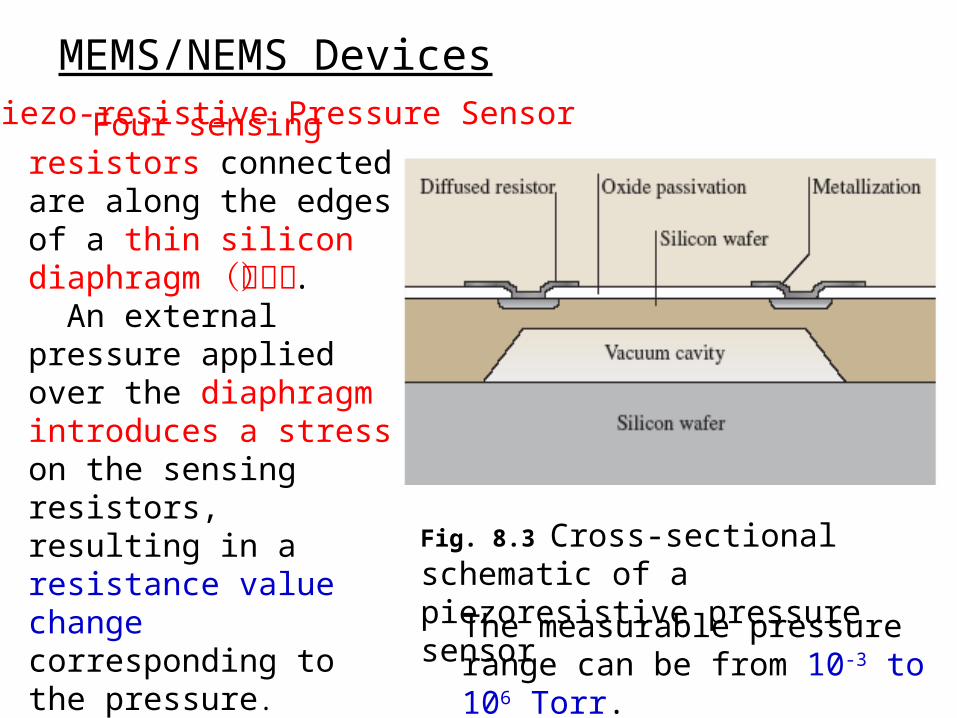
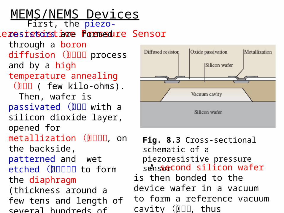
Fig. 8.3 Cross-sectional schematic of a piezoresistive pressure sensor
Four sensing resistors connected are along the edges of a thin silicon diaphragm (隔板) . An external pressure applied over the diaphragm introduces a stress on the sensing resistors, resulting in a resistance value change corresponding to the pressure.
The measurable pressure range can be from 10-3 to 106 Torr.
MEMS/NEMS Devices
Piezo-resistive Pressure Sensor
Fig. 8.3 Cross-sectional schematic of a piezoresistive pressure sensor
First, the piezo-resistors are formed through a boron diffusion (硼扩散) process and by a high temperature annealing (退火) ( few kilo-ohms). Then, wafer is passivated(钝化) with a silicon dioxide layer, opened for metallization(敷金属) , on the backside, patterned and wet etched(湿法光刻) to form the diaphragm (thickness around a few tens and length of several hundreds of micrometers).
A second silicon wafer is then bonded to the device wafer in a vacuum to form a reference vacuum cavity (空腔) , thus completing the sensor.
MEMS/NEMS DevicesPiezo-resistive Pressure Sensor
The piezo-resistive sensors are - simple to fabricate and - can be readily interfaced (接口) with electronic systems. However, the resistors are - temperature dependent and - consume DC power (直流电源) . - Long-term characteristic drift and resistor thermal noise ultimately limit the sensor resolution. .
MEMS/NEMS Devices
Capacitive Sensor
• Capacitive pressure sensors are attractive because they are virtually temperature independent and consume zero DC power. The devices do not exhibit initial turn-on drift and are stable over time.
• Furthermore, CMOS microelectronic circuits can be readily interfaced with the sensors to provide advanced signal conditioning and processing, thus improving overall system performance.
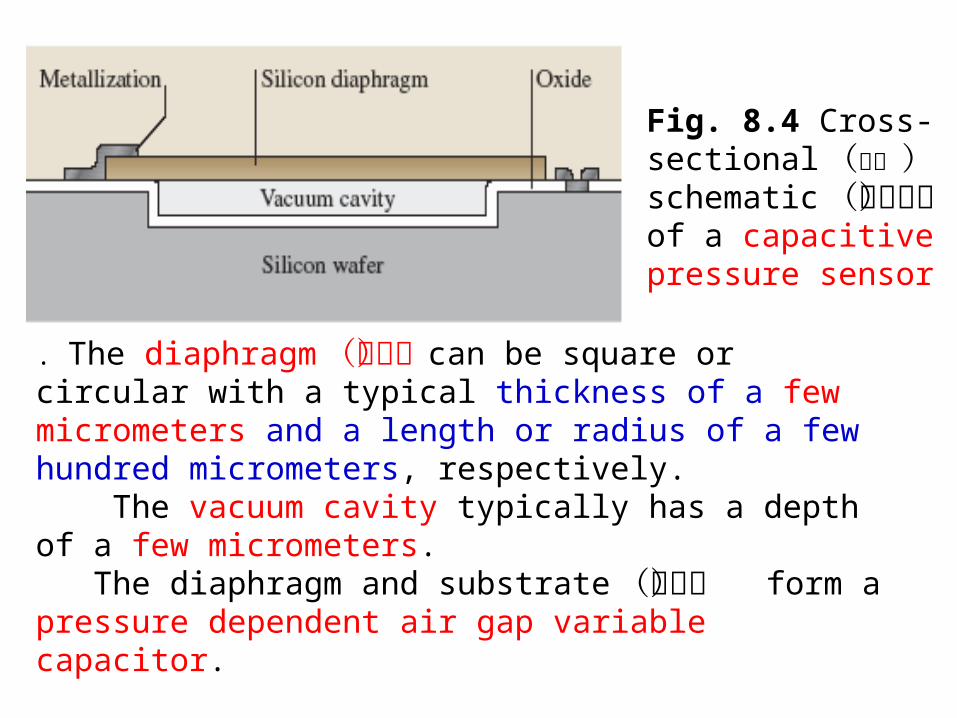
Fig. 8.4 Cross-sectional (断层 ) schematic (原理图) of a capacitive pressure sensor
. The diaphragm (隔板) can be square or circular with a typical thickness of a few micrometers and a length or radius of a few hundred micrometers, respectively. The vacuum cavity typically has a depth of a few micrometers. The diaphragm and substrate (衬底) form a pressure dependent air gap variable capacitor.
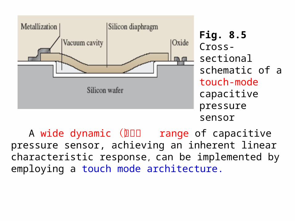
Fig. 8.5 Cross-sectional schematic of a touch-mode capacitive pressure sensor
A wide dynamic (动态) range of capacitive pressure sensor, achieving an inherent linear characteristic response,
can be implemented by employing a touch mode architecture.
MEMS/NEMS Devices
Capacitive Sensor
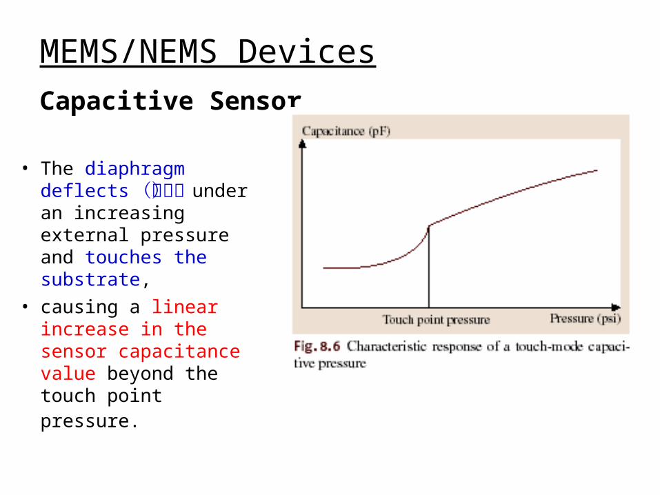
• The diaphragm deflects (偏转) under an increasing external pressure and touches the substrate,
• causing a linear increase in the sensor capacitance value beyond the touch point pressure.
MEMS/NEMS Devices
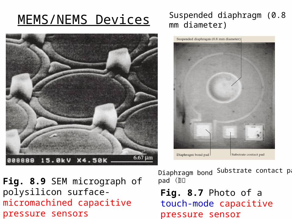
Fig. 8.7 Photo of a touch-mode capacitive pressure sensor
Fig. 8.9 SEM micrograph of polysilicon surface-micromachined capacitive pressure sensors
Suspended diaphragm (0.8 mm diameter)
Diaphragm bond pad(垫)
Substrate contact pad
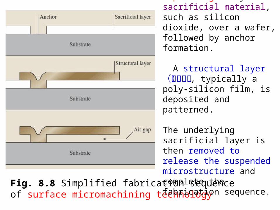
Fig. 8.8 Simplified fabrication sequence of surface micromachining technology
The process starts by depositing a layer of sacrificial material, such as silicon dioxide, over a wafer, followed by anchor formation.
A structural layer (结构层) , typically a poly-silicon film, is deposited and patterned.
The underlying sacrificial layer is then removed to release the suspended microstructure and complete the fabrication sequence.
MEMS/NEMS Devices inertial sensors
• Micro-machined inertial (惯性) sensors, silicon-based MEMS sensors, consist of accelerometers (加速度传感器) and gyroscopes (回转仪) and have been successfully commercialized.
• Inertial sensors fabricated by micromachining technology can achieve reduced size, weight, and cost, all which are critical for consumer applications.
• More importantly, these sensors can be integrated with microelectronic circuits to achieve a functional micro-system with high performance.
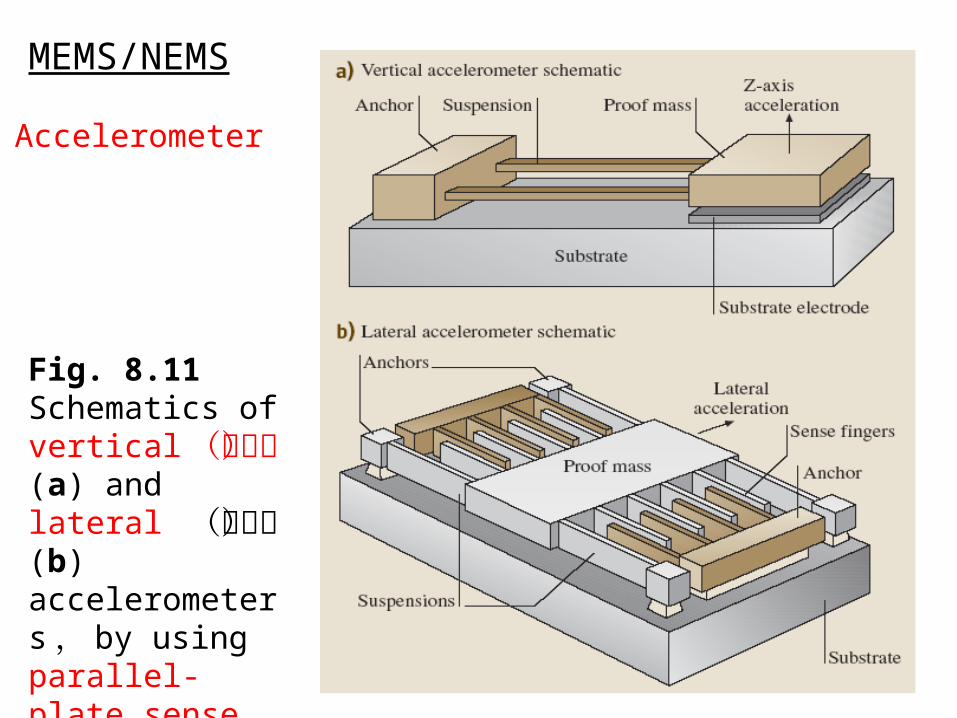
MEMS/NEMS
Fig. 8.11 Schematics of vertical (垂直) (a) and lateral (水平) (b) accelerometers ,by using parallel-plate sense capacitance
Accelerometer
MEMS/NEMS
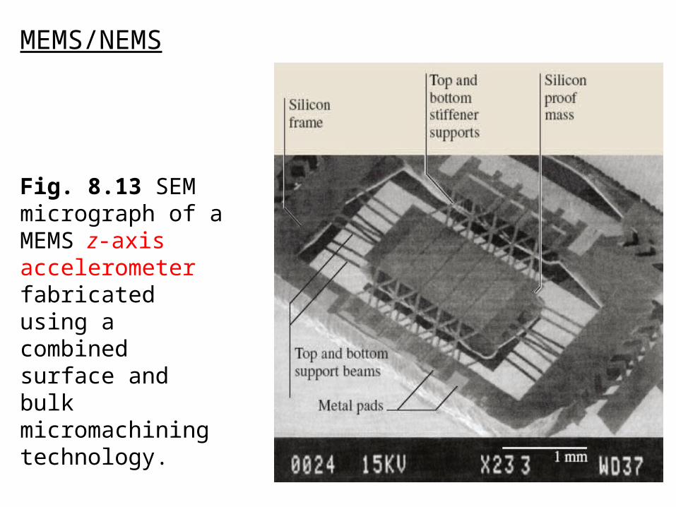
Fig. 8.13 SEM micrograph of a MEMS z-axis accelerometerfabricated using a combined surface and bulk micromachining technology.
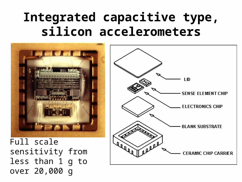
Integrated capacitive type, silicon accelerometers
Full scale sensitivity from less than 1 g to over 20,000 g
MEMS/NEMS
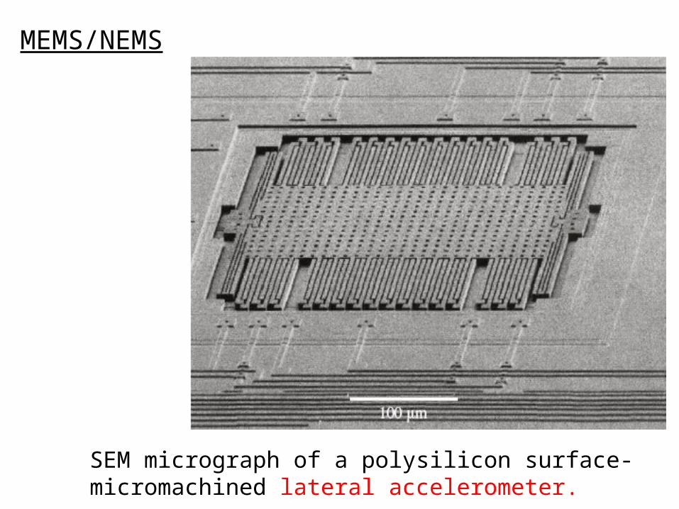
SEM micrograph of a polysilicon surface-micromachined lateral accelerometer.
MEMS/NEMS Devices
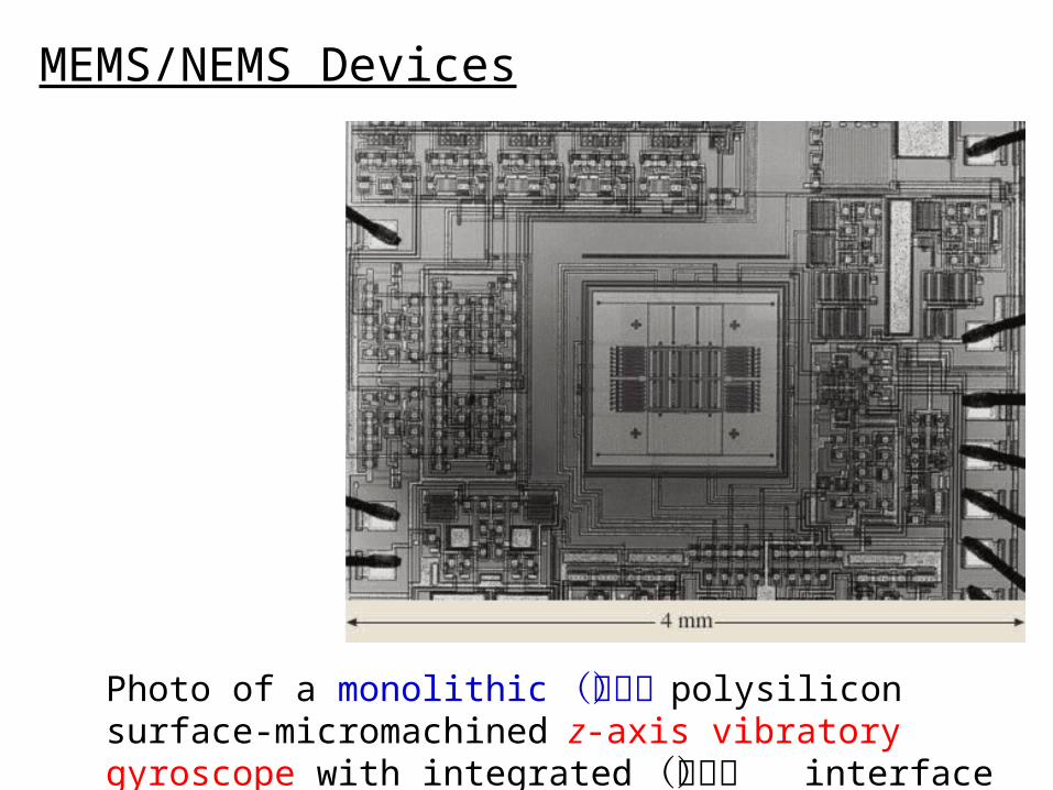
Photo of a monolithic (单片) polysilicon surface-micromachined z-axis vibratory gyroscope with integrated(集成) interface and control electronics
MEMS/NEMS Devices
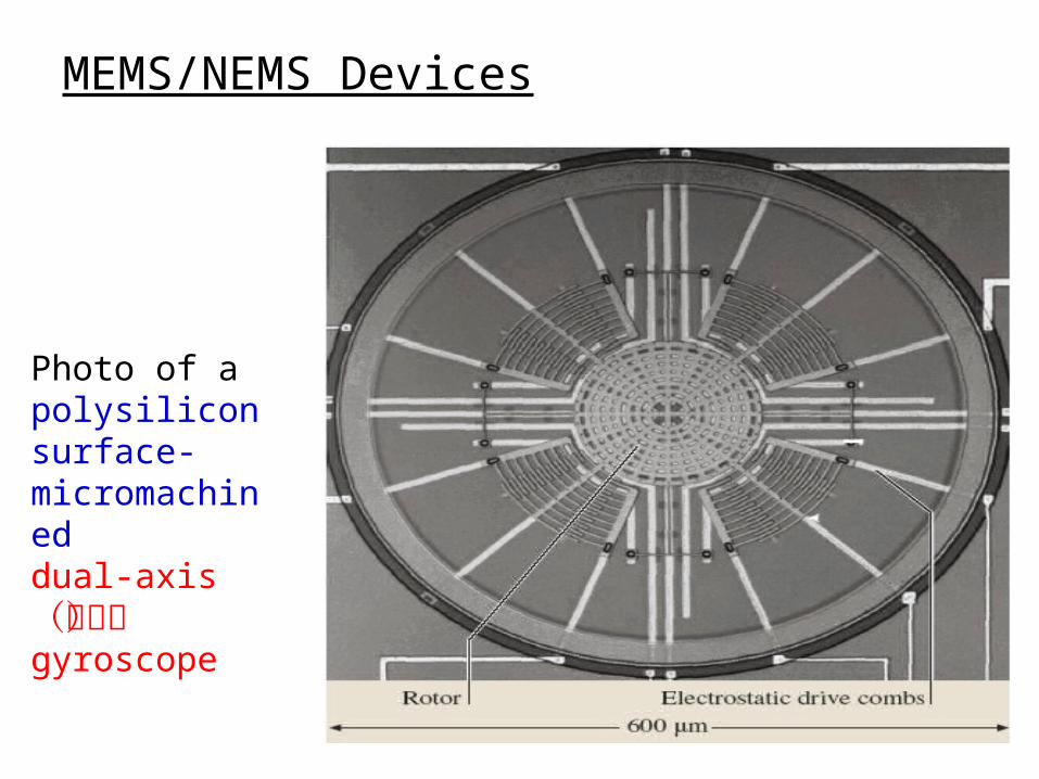
Photo of a polysilicon surface-micromachineddual-axis (双轴) gyroscope
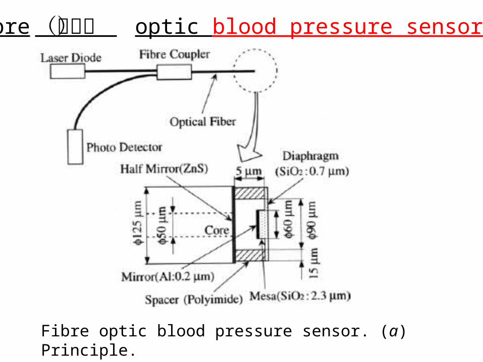
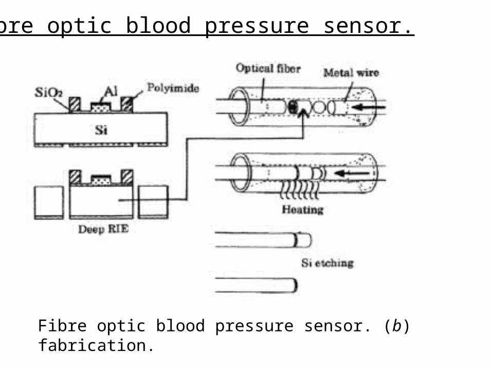
Fibre (纤维) optic blood pressure sensor.
Fibre optic blood pressure sensor. (a) Principle.
Fibre optic blood pressure sensor.
Fibre optic blood pressure sensor. (b) fabrication.
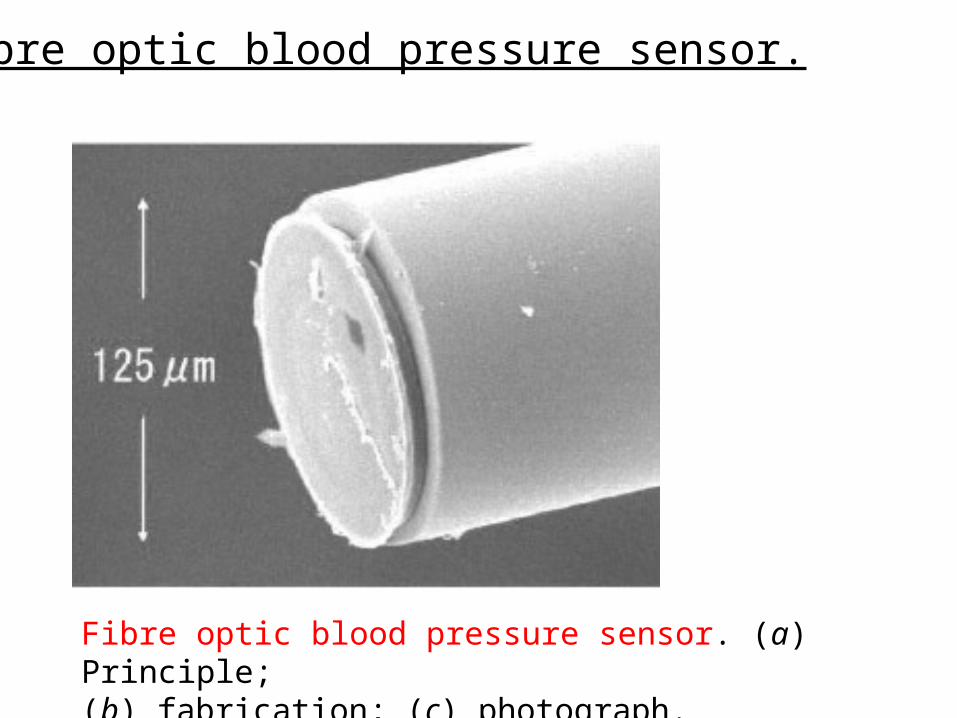
Fibre optic blood pressure sensor. (a) Principle;(b) fabrication; (c) photograph.
Fibre optic blood pressure sensor.
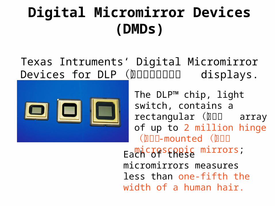
Digital Micromirror Devices (DMDs)
Texas Intruments‘ Digital Micromirror Devices for DLP (数字光处理技术) displays.
The DLP™ chip, light switch, contains a rectangular (矩形) array of up to 2 million hinge(铰链) -mounted (悬挂) microscopic mirrors;
Each of these micromirrors measures less than one-fifth the width of a human hair.
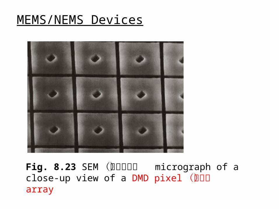
Fig. 8.23 SEM (扫描电镜) micrograph of a close-up view of a DMD pixel (像素) array
MEMS/NEMS Devices
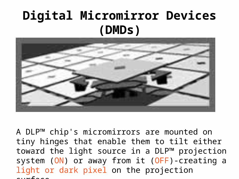
Digital Micromirror Devices (DMDs)
A DLP™ chip's micromirrors are mounted on tiny hinges that enable them to tilt either toward the light source in a DLP™ projection system (ON) or away from it (OFF)-creating a light or dark pixel on the projection surface.
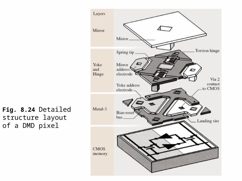
Fig. 8.24 Detailed structure layout of a DMD pixel
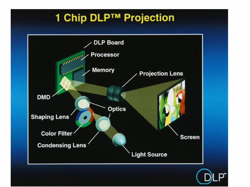
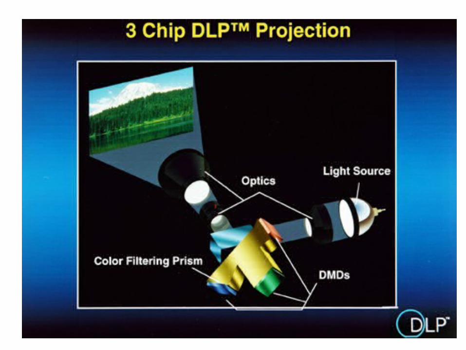
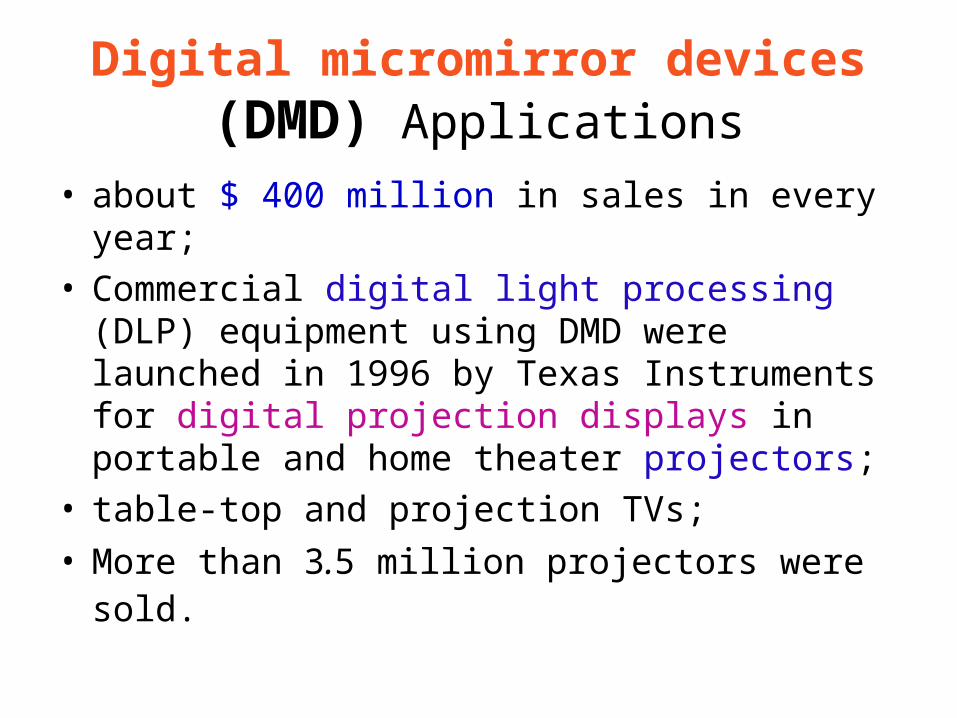
Digital micromirror devices (DMD) Applications
• about $ 400 million in sales in every year; • Commercial digital light processing (DLP)
equipment using DMD were launched in 1996 by Texas Instruments for digital projection displays in portable and home theater projectors;
• table-top and projection TVs;
• More than 3.5 million projectors were sold.
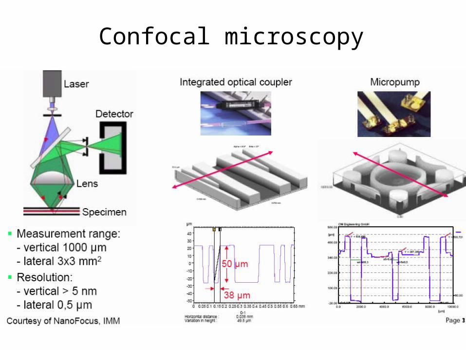
Confocal microscopy
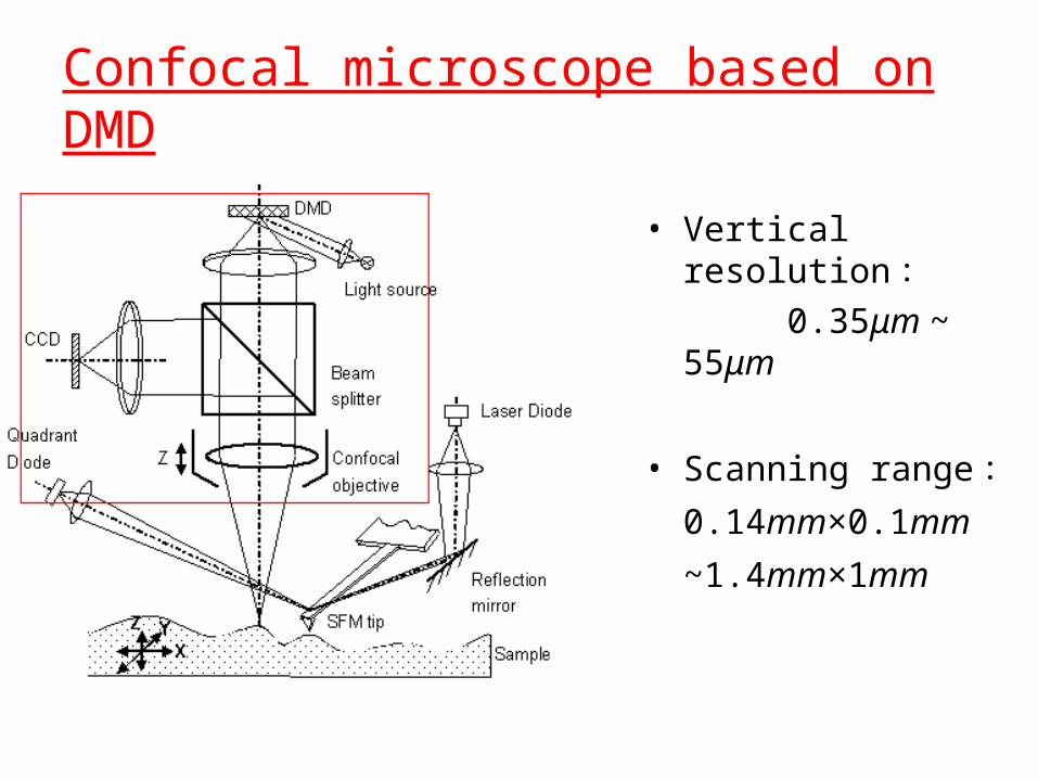
Confocal microscope based on DMD
• Vertical resolution :0.35μm ~
55μm
• Scanning range :0.14mm×0.1mm
~1.4mm×1mm
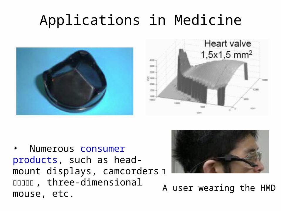
Applications in Medicine
A user wearing the HMD
• Numerous consumer products, such as head-mount displays, camcorders 可携式摄像机 , three-dimensional mouse, etc.
MEMS Fabrication Techniques
Karlsruhe Research Center NSLS/BNL
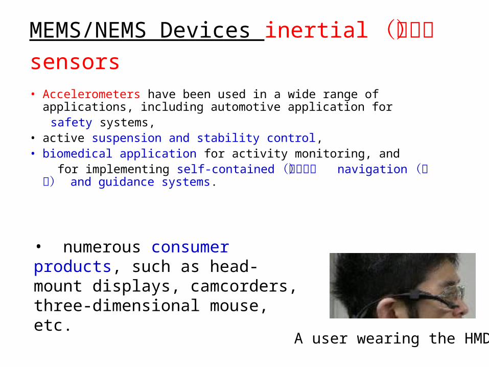
MEMS/NEMS Devices inertial (惯性) sensors • Accelerometers have been used in a wide range of applications, including
automotive application for safety systems, • active suspension and stability control, • biomedical application for activity monitoring, and for implementing self-contained (自容式) navigation (导航) and
guidance systems.
A user wearing the HMD
• numerous consumer products, such as head-mount displays, camcorders, three-dimensional mouse, etc.
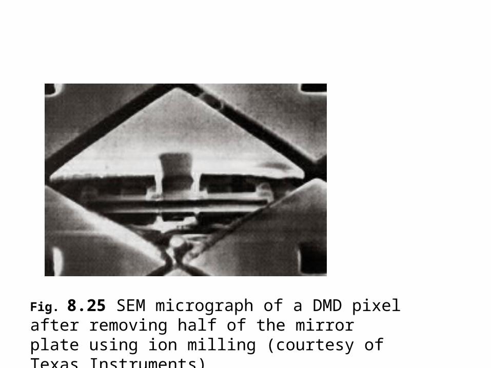
Fig. 8.25 SEM micrograph of a DMD pixel after removing half of the mirror plate using ion milling (courtesy of Texas Instruments)
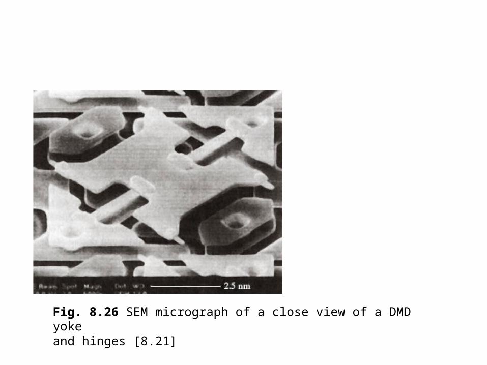
Fig. 8.26 SEM micrograph of a close view of a DMD yokeand hinges [8.21]
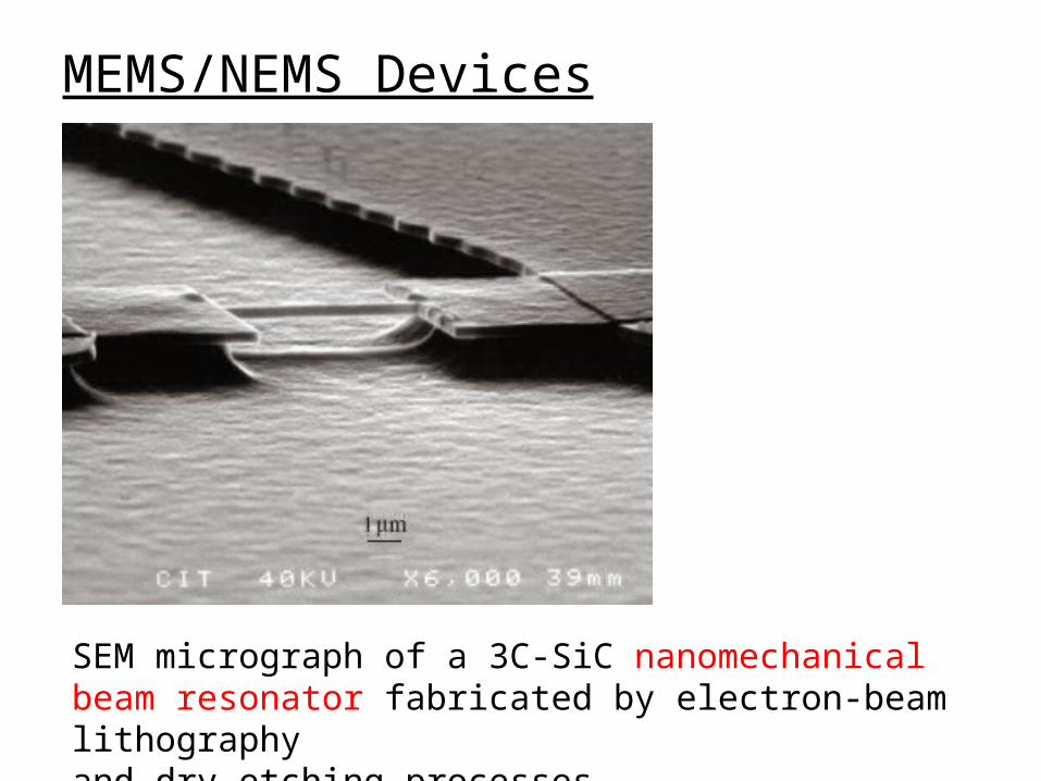
SEM micrograph of a 3C-SiC nanomechanical beam resonator fabricated by electron-beam lithography and dry etching processes
MEMS/NEMS Devices
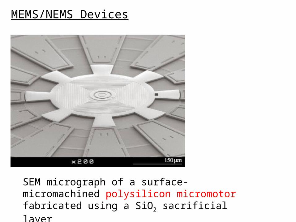
SEM micrograph of a surface-micromachined polysilicon micromotor fabricated using a SiO2 sacrificial layer
MEMS/NEMS Devices
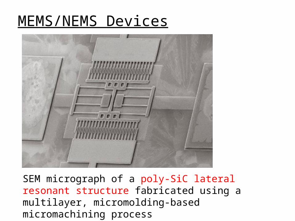
SEM micrograph of a poly-SiC lateral resonant structure fabricated using a multilayer, micromolding-based micromachining process
MEMS/NEMS Devices
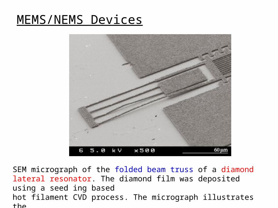
SEM micrograph of the folded beam truss of a diamond lateral resonator. The diamond film was deposited using a seed ing based hot filament CVD process. The micrograph illustrates the challenges currently facing diamond
MEMS/NEMS Devices
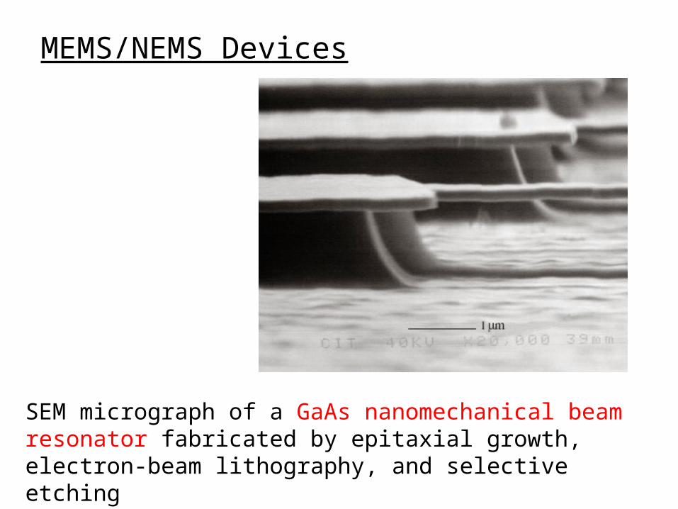
SEM micrograph of a GaAs nanomechanical beam resonator fabricated by epitaxial growth, electron-beam lithography, and selective etching
MEMS/NEMS Devices
MEMS Fabrication Techniques
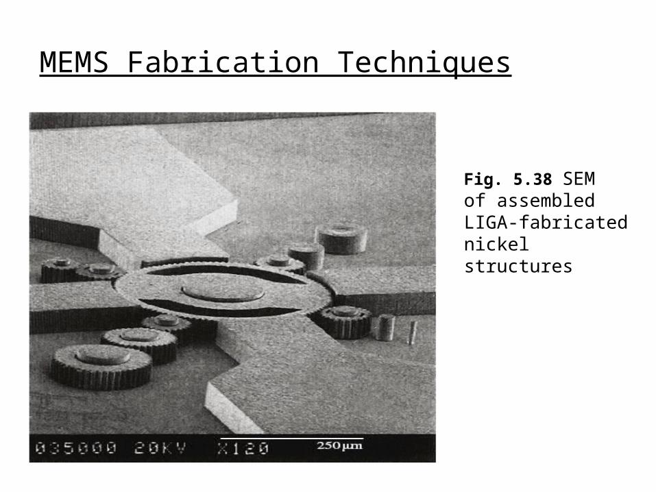
Fig. 5.38 SEMof assembled LIGA-fabricated nickel structures