Single Crystal Diamond NEMS Switch Meiyong Liao Optical and Electronic Materials Unit National Institute for Materials Science, Japan

Welcome message from author
This document is posted to help you gain knowledge. Please leave a comment to let me know what you think about it! Share it to your friends and learn new things together.
Transcript

Single Crystal Diamond NEMS Switch
Meiyong LiaoOptical and Electronic Materials Unit
National Institute for Materials Science, Japan

普段の生活のエネルギー消費を減らす必要!
ナノマシンスイチ:省エネルギー技術(ゼロ)として期待 。
待機電力消費---半導体スイッチ
機器が非使用状態、若しくは何らかの入力(命令指示)待ちの時に定常的に消費している電力
平成20年度
1-5 W
5-10W

MEMS switch: Merits
Poor
Poor
Poor(<25dB)
Large (>1dB)
Fast (10ns)
>1 uW
Large
Semiconductor switch
Excellent
Excellent
Good(>30dB)
Small(<0.2dB)
Slow (10µs)
~0
zero
MEMS switch
High and low temperatures
Linearity
Isolation
Insertion loss
Speed
Power loss
Leakage
Property
Advantages over semiconductor devices
But, poor reliability due to (i) Surface stiction(ii) Mechanical abrasion
Semiconductor devices consume power in OFF state!
VGVD
A
カンチレバー
ドレイン ゲート
ソース
OFF state
VD
A
VG
ドレイン ゲート
ソース
ON stateMEMS switch

Diamond MEMS: route toward high reliability and high performance
2 3 4 5 6 7 8
2500
5000
7500
10000
12500
15000
17500
20000
2L
dEfρ
∝
GaN
ZnO
Ni
Si3N
4
Si
Au
SiC
Diamond
AlN
W
Fe
Accoust
ic v
elo
city
(m/s)
Lattice constant (A)
The highest Young’s modulus
The lowest friction coefficient
Hydrophobic surface
Highest thermal conductivity
Tunable electrical conductivityThe best material
Merits
Current MEMS: intrinsic limitations !!

Challenges and Strategies in Diamond MEMS
What process….? What device concept……?
DifficultiesBatch fabrication of single crystal diamond MEMS structures.Lack of device concepts compatible with the fabrication
process.
AimsEstablish unique process for diamond MEMS structures. Develop high-performance diamond MEMS/NEMS devices.Create novel device concepts.
StrategiesNo direct deposition of diamond on sacrificial layers. Diamond-on-Diamond lateral device concept.

Diamond growthMPCVD
Parameters:Gas: H2 (500 sccm), CH4 (0.4 sccm)RF Power: 400 WPressure: 80 TorrSub. Tem: 900-950oC[B]:1000 ppm 1020cm-3
Substrate: Ib (100)---100 ppm nitrogenThickness: 0.1-0.5µm

Batch production of micro-scale M/NEMS structures
air gap
M. Y. Liao, et al, J. Micromech. Mircoeng. 20,085002 (2010)
W=400nm
W=200nm
W=200nm
M. Y. Liao, et al,Advanced Materials 22, 5393 (2010)

Quality of the MEMS/NEMS structure
1000 1100 1200 1300 1400 1500 16000.2
0.3
0.4
0.5
0.6
0.7
Inte
nsi
ty (
a.u.)
Wavenumber (cm-1)
260 280 300 320 340 360 380
π∗
Counts
(a.
u.)
Energy loss (eV)
Protection Pt layer
Boron doped diamond
diamond
graphite
diamond
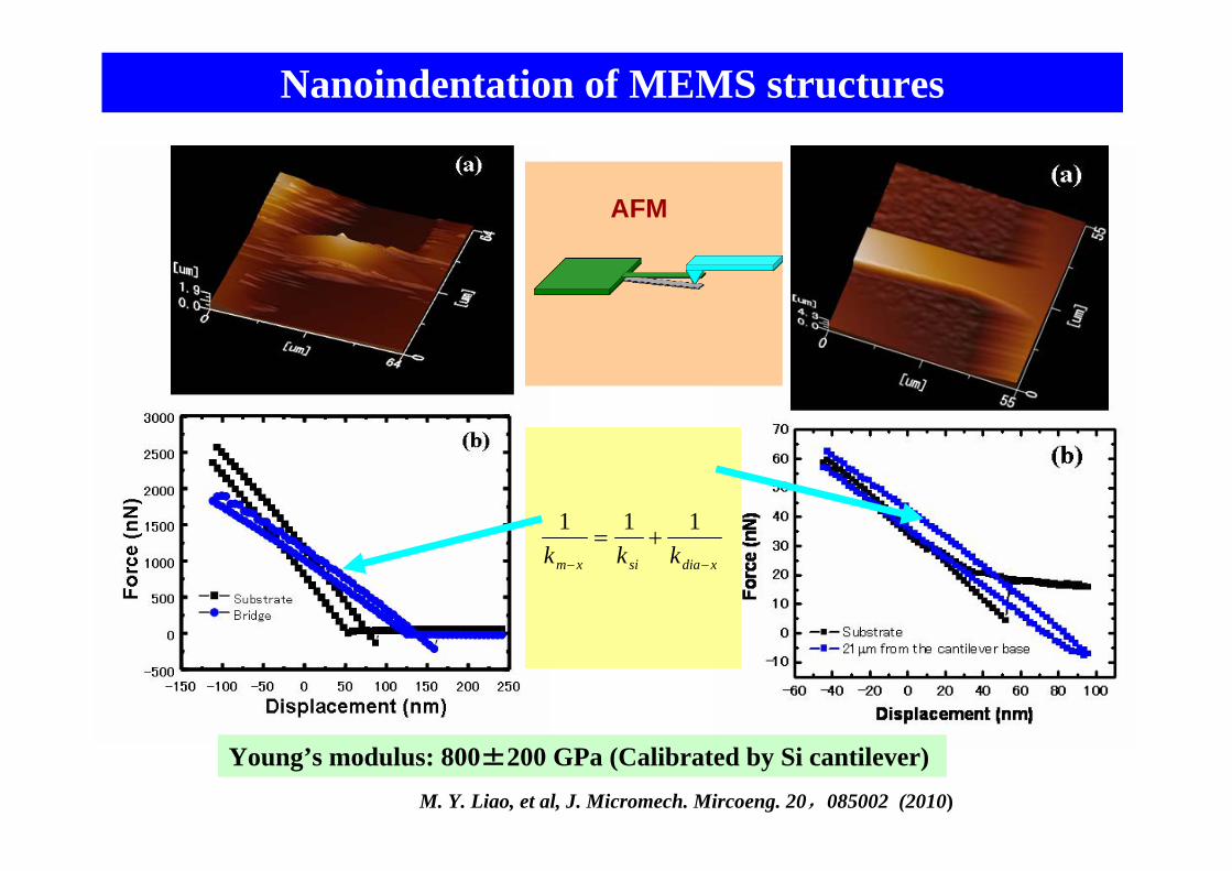
Nanoindentation of MEMS structures
Young’s modulus: 800±200 GPa (Calibrated by Si cantilever)
xdiasixm kkk −−
+=111
AFM
M. Y. Liao, et al, J. Micromech. Mircoeng. 20,085002 (2010)

Nanoelectromechanical switch: 2-terminal
0 2 4 6 8 10 12 14 16 18 2010-14
10-13
10-12
10-11
10-10
10-9
Cur
rent
(A)
Voltage (V)0 10 20 30 40 50 60 70 80
10-14
10-13
10-12
10-11
10-10
10-9
10-8
10-7
10-6
10-5
Curr
ent
(A)
Voltage (V)0 5 10 15 20
10-14
10-13
10-12
10-11
10-10
10-9
10-8
Cur
rent
(A)
Voltage (V)
A A A

Nanoelectromechanical switch: 3-terminal
-80 -60 -40 -20 010-16
10-14
10-12
10-10
10-8
1st 2nd 3rd
Dra
in c
urre
nt (A
)
Gate voltage (V)-80 -60 -40 -20 0 20 40 60 80
10-13
10-12
10-11
10-10
10-9
10-8
Dain voltage =10 V
Dra
in c
urre
nt (A
)
Gate Voltage (V)
2µm
5µmON-stateOFF-state
VG
A
D
VD
G
S
0 50 100 150 20010-14
10-13
10-12
10-11
10-10
Cur
rent
(A)
Time (s)
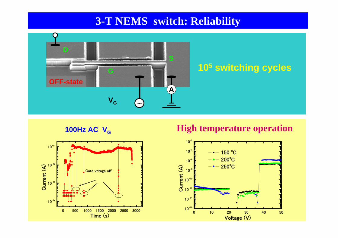
3-T NEMS switch: Reliability
S
G
D
OFF-state
~VG
A
105 switching cycles
0 500 1000 1500 2000 2500 3000
10-14
10-13
10-12
10-11
Gate votage off
Curr
ent
(A)
Time (s)
100Hz AC VG
0 10 20 30 40 5010-16
10-14
10-12
10-10
10-8
10-6
10-4
10-2
150 oC
200oC
250oC
Curr
ent
(A)
Voltage (V)
High temperature operation

Modeling and simulation of NEMS switch
Gate DrainSource
0V)(ε =∇⋅∇−
Tes DE)(nnD)(E
21F ⋅+⋅−=
Potential in the air around the beam
Fes: Electrostatic force density of the beamE: electric field, D: displacement vector
Pull-in voltage: defined as the beam contact to the gate.L: length, W: width, t: thickness
B=E0t3g3
)Wgc(1cLε
B4cV3
22
40
1inpull
+=−
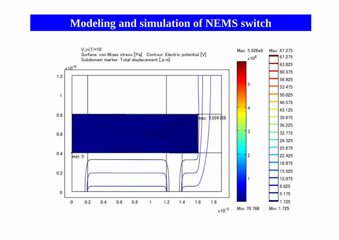
Modeling and simulation of NEMS switch

Comparison between experiment and simulation:
0 10 20 30 40 500
20
40
60
80
Pul
l in
voltag
e (
V)
Drain voltage (V)
0 10 20 30 40 50 60 70 80 900
200
400
600
800
1000
Str
ess
(M
Pa)
Gate voltage (V)
High Young’s ModulusGood reproducibility Consistence between experiment and simulationYoung’s modulus=1100GPa
Joint stress much lowerthan fracture strength
Drain voltage affecting pull-in voltage

Applications of diamond M/NEMS Switch: H4
携帯電話や無線LANなどの無線通信
耐環境デバイス:高温論理回路
メモリ
(待機ゼロ)電源制御装置
ナノ・マクロマシンスイッチ
High
power Hightemperature
High
frequencyHighreliability

Summary
For the first time
Single-crystal diamond NEMS switch was fabricated.
Batch production of SCD MEMS/NEMS structures were developed.
The diamond NEMS switches exhibit high performance.(1) High controllability .(2) High reproducibility.(3) Good reliability.
Modeling and simulation were made and were consistent with experiments
Related Documents