Proof Copy Mechanical Properties of Ultrananocrystalline Diamond Thin Films Relevant to MEMS/NEMS Devices by H.D. Espinosa, B.C. Prorok, B. Peng, K.H. Kim, N. Moldovan, O. Auciello, J.A. Carlisle, D.M. Gruen, and D.C. Mancini ABSTRACT—The mechanical properties of ultrananocrys- talline diamond (UNCD) thin films were measured using mi- crocantilever deflection and membrane deflection techniques. Bending tests on several free-standing UNCD cantilevers, 0.5 µm thick, 20 µm wide and 80 µm long, yielded elastic modulus values of 916–959 GPa. The tests showed good re- producibility by repeated testing on the same cantilever and by testing several cantilevers of different lengths. The largest source of error in the method was accurate measurement of film thickness. Elastic modulus measurements performed with the novel membrane deflection experiment (MDE), developed by Espinosa and co-workers, gave results similar to those from the microcantilever-based tests. Tests were performed on UNCD specimens grown by both micro and nano wafer- seeding techniques. The elastic modulus was measured to be between 930–970 GPa for the microseeding and between 945–963 GPa for the nanoseeding technique. The MDE test also provided the fracture strength, which for UNCD was found to vary from 0.89 to 2.42 GPa for the microseeded samples and from 3.95 to 5.03 for the nanoseeded samples. The nar- rowing of the elastic modulus variation and major increase in fracture strength is believed to result from a reduction in sur- face roughness, less stress concentration, when employing the nanoseeding technique. Although both methods yielded reliable values of elastic modulus, the MDE was found to be more versatile since it yielded additional information about the structure and material properties, such as strength and initial stress state. KEY WORDS—AUTHOR: PLEASE PROVIDE Introduction Silicon has been the dominant material in the micro- electronics revolution of the 20th century and has been the precursor to the microelectromechanical/ nanoelec- tromechanical systems (MEMS/NEMS) revolution currently H.D. Espinosa is a (TITLE), B.C. Prorok is a (TITLE), B. Peng is a (TITLE), and K.H. Kim is a (TITLE), Department of Mechanical Engineering, Northwestern University, Evanston, IL 60208-3111. N. Moldovan is a (TITLE), O. Auciello is a (TITLE), J.A. Carlisle is a (TITLE), D.M. Gruen is a (TITLE), and D.C. Mancini is a (TITLE), Materials Science and Experimental Facilities Divisions, Argonne National Laboratory, Argonne, IL 60439. H.D. Espinosa is the author to whom correspondence should be addressed: [email protected]. Original manuscript submitted: xxx. Final manuscript received: xxx. underway. It has been the material of choice for current MEMS devices, mainly because devices can be fashioned using standard microfabrication techniques. 1,2 However, Si is not the best choice for devices where friction and wear are present since its poor mechanical and tribological properties limit its performance. 3,4 Thus, new and robust materials with exceptional and tailorable properties must be sought to meet the stringent demands that MEMS/NEMS devices require. Diamond Films for Micro and Nano Devices Carbon in its various forms, specifically diamond, may be- come a key material for the manufacturing of MEMS/NEMS devices in the 21st century. The new ultrananocrystalline di- amond (UNCD) developed at Argonne National Laboratory 5 is emerging as one of the most promising forms of dia- mond with unique multifunctional properties. The UNCD films are grown using a microwave plasma chemical vapor deposition (CVD) technique involving a new CH 4 /Ar chem- istry. The process yields films with extremely small grain size (2–5 nm), significantly smaller than nanocrystalline di- amond films (30–100 nm grain size) produced by the con- ventional CH 4 /H chemistry. 6,7 The films possess many of the outstanding physical properties of diamond, i.e., they ex- hibit exceptional hardness, extremely low friction coefficient and wear, high thermal and electrical conductivity (the latter when doped with nitrogen 8 ), high electrical resistance when grown with hydrogen addition to the CH 4 /Ar plasma, and high chemical inertness, optical transmittance, electrical car- rier mobility, and dielectric breakdown strength. UNCD is characterized by a unique microstructure of sp 3 - bonded grains and atomic grain boundaries (2–4 Å) with sub- stantial sp 2 coordination. Preliminary results have shown that this unique microstructure results in outstanding mechanical properties (∼97 GPa hardness and 967 GPa Young’s mod- ulus, which are similar to single-crystal diamond 9 ), unique tribological properties (coefficient of friction of the order of ∼0.02–0.03 10 ), and field-induced electron emission (thresh- old voltage ∼2–3 V µm −1 11 ). In addition, n-type doping of UNCD thin films, a long sought goal of researchers in diamond thin-film research, has been demonstrated, further broadening the range of applications of UNCD by achiev- ing significant electrical conduction via nitrogen doping. 8,12 UNCD also exhibits unique inert electrochemical and bio- compatible properties that make it suitable for biological applications. 13 Preliminary work by investigators at Argonne National Laboratory has demonstrated the feasibility of fabricating © 2003 Society for Experimental Mechanics Experimental Mechanics • 1

Welcome message from author
This document is posted to help you gain knowledge. Please leave a comment to let me know what you think about it! Share it to your friends and learn new things together.
Transcript

Proo
f Cop
y
Mechanical Properties of Ultrananocrystalline DiamondThin Films Relevant to MEMS/NEMS Devices
by H.D. Espinosa, B.C. Prorok, B. Peng, K.H. Kim, N. Moldovan, O. Auciello,J.A. Carlisle, D.M. Gruen, and D.C. Mancini
ABSTRACT—The mechanical properties of ultrananocrys-talline diamond (UNCD) thin films were measured using mi-crocantilever deflection and membrane deflection techniques.Bending tests on several free-standing UNCD cantilevers,0.5 µm thick, 20 µm wide and 80 µm long, yielded elasticmodulus values of 916–959 GPa. The tests showed good re-producibility by repeated testing on the same cantilever andby testing several cantilevers of different lengths. The largestsource of error in the method was accurate measurement offilm thickness. Elastic modulus measurements performed withthe novel membrane deflection experiment (MDE), developedby Espinosa and co-workers, gave results similar to thosefrom the microcantilever-based tests. Tests were performedon UNCD specimens grown by both micro and nano wafer-seeding techniques. The elastic modulus was measured tobe between 930–970 GPa for the microseeding and between945–963 GPa for the nanoseeding technique. The MDE testalso provided the fracture strength, which for UNCD was foundto vary from 0.89 to 2.42 GPa for the microseeded samplesand from 3.95 to 5.03 for the nanoseeded samples. The nar-rowing of the elastic modulus variation and major increase infracture strength is believed to result from a reduction in sur-face roughness, less stress concentration, when employingthe nanoseeding technique. Although both methods yieldedreliable values of elastic modulus, the MDE was found to bemore versatile since it yielded additional information about thestructure and material properties, such as strength and initialstress state.
KEY WORDS—AUTHOR: PLEASE PROVIDE
Introduction
Silicon has been the dominant material in the micro-electronics revolution of the 20th century and has beenthe precursor to the microelectromechanical/ nanoelec-tromechanical systems (MEMS/NEMS) revolution currently
H.D. Espinosa is a (TITLE), B.C. Prorok is a (TITLE), B. Peng isa (TITLE), and K.H. Kim is a (TITLE), Department of MechanicalEngineering, Northwestern University, Evanston, IL 60208-3111. N.Moldovan is a (TITLE), O. Auciello is a (TITLE), J.A. Carlisle is a(TITLE), D.M. Gruen is a (TITLE), and D.C. Mancini is a (TITLE),Materials Science and Experimental Facilities Divisions, Argonne NationalLaboratory, Argonne, IL 60439. H.D. Espinosa is the author to whomcorrespondence should be addressed: [email protected].
Original manuscript submitted: xxx.Final manuscript received: xxx.
underway. It has been the material of choice for currentMEMS devices, mainly because devices can be fashionedusing standard microfabrication techniques.1,2 However, Siis not the best choice for devices where friction and wear arepresent since its poor mechanical and tribological propertieslimit its performance.3,4 Thus, new and robust materials withexceptional and tailorable properties must be sought to meetthe stringent demands that MEMS/NEMS devices require.
Diamond Films for Micro and Nano Devices
Carbon in its various forms, specifically diamond, may be-come a key material for the manufacturing of MEMS/NEMSdevices in the 21st century. The new ultrananocrystalline di-amond (UNCD) developed at Argonne National Laboratory5
is emerging as one of the most promising forms of dia-mond with unique multifunctional properties. The UNCDfilms are grown using a microwave plasma chemical vapordeposition (CVD) technique involving a new CH4/Ar chem-istry. The process yields films with extremely small grainsize (2–5 nm), significantly smaller than nanocrystalline di-amond films (30–100 nm grain size) produced by the con-ventional CH4/H chemistry.6,7 The films possess many ofthe outstanding physical properties of diamond, i.e., they ex-hibit exceptional hardness, extremely low friction coefficientand wear, high thermal and electrical conductivity (the latterwhen doped with nitrogen8), high electrical resistance whengrown with hydrogen addition to the CH4/Ar plasma, andhigh chemical inertness, optical transmittance, electrical car-rier mobility, and dielectric breakdown strength.
UNCD is characterized by a unique microstructure of sp3-bonded grains and atomic grain boundaries (2–4 Å) with sub-stantial sp2 coordination. Preliminary results have shown thatthis unique microstructure results in outstanding mechanicalproperties (∼97 GPa hardness and 967 GPa Young’s mod-ulus, which are similar to single-crystal diamond9), uniquetribological properties (coefficient of friction of the order of∼0.02–0.0310), and field-induced electron emission (thresh-old voltage ∼2–3 V µm−1 11). In addition, n-type dopingof UNCD thin films, a long sought goal of researchers indiamond thin-film research, has been demonstrated, furtherbroadening the range of applications of UNCD by achiev-ing significant electrical conduction via nitrogen doping.8,12
UNCD also exhibits unique inert electrochemical and bio-compatible properties that make it suitable for biologicalapplications.13
Preliminary work by investigators at Argonne NationalLaboratory has demonstrated the feasibility of fabricating
© 2003 Society for Experimental Mechanics Experimental Mechanics • 1

Proo
f Cop
y
two-dimensional (2D) and three-dimensional (3D) MEMScomponents that can be the basis for the fabrication of com-plete MEMS/NEMS devices.11,14,15 Components, such ascantilevers, and multilevel devices, such as microturbines,have already been produced. These preliminary develop-ments are promising steps toward full-scale application ofUNCD components in functional MEMS devices. However,before full-scale integration can occur, several intrinsic mate-rial properties, such as elastic modulus, plasticity and fractureof undoped and doped UNCD, must be well characterized tofully exploit the potential of this material.
Microscale Mechanical Testing
Several mechanical testing schemes exist for examiningthe microscale mechanical properties of materials and struc-tures. Extensive reviews exist on the subject.16–18 Bendingtests on micromachined beams were first performed by Weihset al.19 and repeated by others.20,21 The method involves de-flecting a cantilever-like beam fixed at one end to the sub-strate. A nanoindenter is used to deflect the beam and mea-sures the load–deflection response. From this information, thestiffness of the beam is found and can be used to determine theelastic modulus of the material. Special attention should beplaced on accurately measuring the beam dimensions as wellas designing dimensions and testing conditions to minimizeboundary, Poisson, and stress concentration effects.
The membrane deflection experiment (MDE), developedby Espinosa et al.,22–24 is a novel microscale mechanical testfor evaluating elasticity, plasticity, and fracture of thin films.It works by stretching a free-standing thin-film membrane ina fixed–fixed configuration where the membrane is attachedat both ends and spans a micromachined window beneath; seeFig. 1(a). A nanoindenter applies a line-load at the center ofthe span to achieve deflection. Simultaneously, deflection isrecorded by the nanoindenter displacement sensor and by aninterferometer focused on the bottom side of the membranethrough-view window in the wafer; see Fig. 1(b). The geom-etry of the membranes is such that it contains tapered regionsto eliminate boundary failure effects. The basic architecturecan be described as double-dog-bone. The result is direct ten-sion, in the absence of strain gradients, of the gaged region.From this measurement, we determine mechanical propertiessuch as Young’s modulus, residual stress state, and yield andfracture stresses.
In this paper, we use microcantilever deflection and themembrane deflection experiment techniques to gain a betterunderstanding of the elastic modulus and strength of UNCDthin films. We have taken special care to design differentspecimen characteristics for each technique in an attempt tominimize effects in each that may hinder accurate propertymeasurements.
Experimental Procedure
Specimen Design
Two types of specimens were used in this study. The first isa free-standing, thin-film cantilever structure made of UNCDwith film thickness ranging from 0.55 to 0.65 µm. The film isgrown directly onto a Si substrate as described below. Figure 2shows a 3D schematic view of the cantilever structure. Thedimensions of the cantilever are defined on the figure with tas the thickness, b as the width (20 µm for all cantilevers),
PV
Wafer
Optics
MirauMicroscopeObjective
PMPM
θ
LM
∆(b)
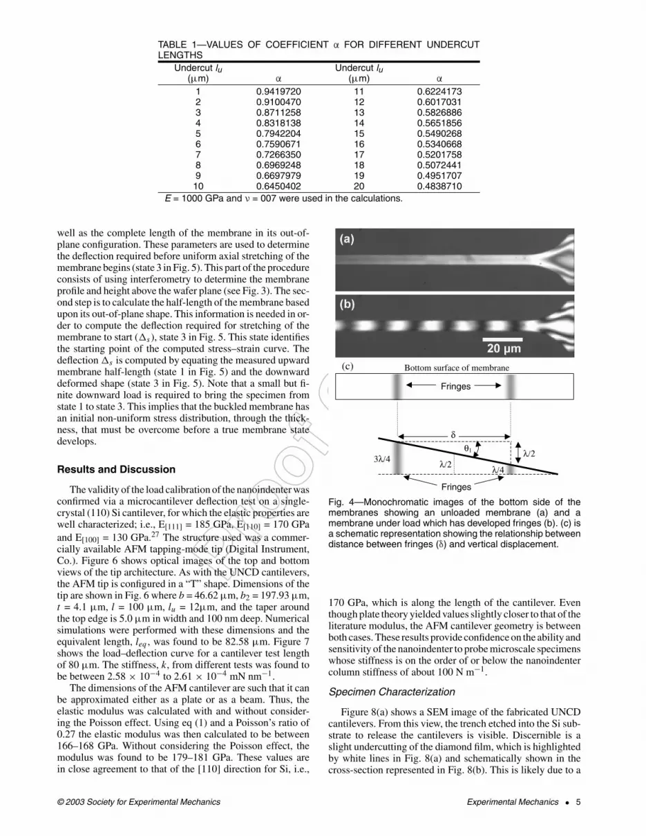
Fig. 1—(a) Optical image of three as-microfabricated MDEmembranes; (b) side view of the MDE test showing verticalload being applied by the nanoindenter, PV, the membranein-plane load, PM, and the position of the Mirau microscopeobjective
l
tb
UNCD Film
Si Substrate
Undercut
Fig. 2—Schematic 3D view of a free-standing cantileverstructure. Geometric parameters are defined in the text.
and l as the cantilever length at the point of contact duringdeflection. The overall length of the cantilevers is 200 µm.The structure of the cantilevers contained an etching undercutthat resulted in the specimens having a “T” shape (Fig. 2).This is accounted for in the data reduction procedure and isdescribed later. The second type of specimen consists of spe-cially designed double-dog-bone, free-standing membranesas shown in Fig. 1(a). Specimens with a width of ∼13.5 µmwere tested.
UNCD Film Growth and Specimen Microfabrication
The UNCD films were produced by a microwave plasma-assisted CVD technique developed at Argonne National Lab-oratory. Details of the synthesis are given in Gruen.5 The
2 • Vol. 43, No. 3, September 2003 © 2003 Society for Experimental Mechanics
Proo
f Cop
y
procedure yields UNCD films with grains 2–5 nm in diam-eter. UNCD films 0.5–0.6 µm thick were made to fabricatethe cantilevers and the MDE specimens.
The cantilevers and MDE specimens were microfabricatedusing standard procedures. The following is a summary of thesteps used in fabricating the UNCD cantilevers. A similarprocedure was used to fabricate the MDE specimens.
1. Seeding the Si wafer and UNCD growth (0.5–0.6 µm).
2. Deposition of 300 nm Al by sputtering. Al is used asmask material due to its resistance to oxygen RIE.
3. Photoresist spin-coating with S 1805; exposure withKarl Suss MA6; developing; postbaking.
4. Wet chemical etching of Al.
5. O2reactive ion etching (RIE), 50 mTorr, 200 W, untilthe exposed UNCD is etched away. During the etching,the photoresist is also removed. Removal of Al maskusing wet etching.
6. Si wafer KOH etching from the front side (90 min,KOH 30% at 80◦C) using the UNCD pattern as a mask-ing layer. Cantilevers were so released. Underetchingof UNCD cantilevers is possible due to a slight mis-alignment of the Si wafer <110> direction with respectto the cantilever structure.
Characterization Protocol
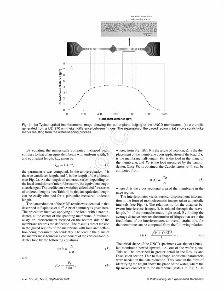
Both cantilever and membrane specimen structures werecharacterized by a variety of techniques. Dimensions of thecantilevers were measured with a translation stage possessinga resolution of 1 µm or better. The thickness of both struc-tures was measured with a discrete wavelength ellipsometerand verified by cross-section scanning electron microscopy(SEM). Characterization of the out-of-plane initial cantilevershape was carried out by scanning the surface with a Mi-croXAM 3-D surface profilometer. Scans were also madeafter testing to identify permanent changes in cantilever de-flection. Both were performed at identical temperature andhumidity conditions. Evaluation of surface roughness wasnecessary to ascertain its effect on determining the cross-sectional area and to ascertain the effect of seeding on theresulting thin-film surface characteristics. Therefore, root-mean-square (rms) values of the film surface roughness weremeasured via atomic force microscopy (AFM).
Due to intrinsic strains and differences in thermal expan-sion coefficient between the UNCD film and the Si substrate,αUNCD = 1.5 × 10⁻⁶ ◦K−1 and αSi = 2.5 × 10⁻⁶ ◦K−1,the membranes exhibited an upward, out-of-plane buckling,shown in Fig. 3(a). The out-of-plane shape was character-ized by interferometry. Figure 3(b) shows a typical profileexhibited by the membranes. This information is valuable indetermining the height and point of contact between the in-denter tip and membrane as well as the deflection where thestraining of the membrane begins, described later in the DataReduction section.
A final feature in the characterization of the UNCD film isnon-uniformities that exist in the specimens due to the waferseeding process required for UNCD deposition. Two seedingprocesses were used in the experiments described in this pa-per. One such process involved mechanical polishing of the
Si substrate surface with micrometer-size diamond powder.This seeding process resulted in diamond particles generat-ing defect sites on the substrate surface that, in turn, initiatedfilm growth and at the same time led to scratch-like markson the surface of the UNCD film; see the optical microscopeimage of a UNCD film in Fig. 3(a). These scratches pro-duce stress concentrations detrimental to the film strength.A second seeding process consisted of the ultrasonic deposi-tion of nanosized diamond powder on the Si substrate. Thisprocess significantly reduced the film roughness and elimi-nated scratch-like features on the surface of the film. We willdiscuss quantitative measurements in the Results section.
Mechanical Testing
Mechanical testing involved deflection of thin-film UNCDcantilevers and stretching of thin-film UNCD membraneswith a nanoindenter. The cantilever deflection was carriedout at different characteristic cantilever lengths and the MDEtest was performed on specimens with different widths. De-tails of the MDE testing procedure were reported in Espinosaet al.22–24 In both techniques, a nanoindenter deflected thespecimens to a prescribed value. Load and deflection arerecorded by the nanoindenter in both cases. For the MDEtests, deflection is also recorded by an interferometer. Al-though the two match well, the interferometer allows the ex-periment to be viewed in situ and important time signaturessuch as point of tip–membrane contact and membrane failureare determined.
Data Reduction
The raw data obtained from the tests were processed to ob-tain the quantities of interest. For instance, in both cantileverand membrane deflection tests the load obtained from thenanoindenter was properly reduced to remove thermal driftand support spring stiffness of the nanoindenter column. Thisprocedure is described elsewhere.22–26 The resulting load–deflection curve was then analyzed using cantilever and mem-brane formulae. In the case of the cantilever tests, the initiallinear part of the curve was used to measure stiffness. Usingthis value and the standard stiffness equation for deflection ofa uniform beam, with plate modulus to account for the largewidth to length ratio, the Young’s modulus of the film wasidentified, namely
k = Eb
4(1 − ν2)
(t
l
)3
, (1)
where k is the stiffness, E is the Young’s modulus, b is thecantilever width, v is the Poisson’s ratio, t is the thicknessand l is the length of the cantilever at the point of contact.However, since the Poisson’s ratio for diamond is 0.07, thePoisson effect can be ignored and the equation becomes thatof a uniform beam.
In order to account for the T-shaped geometry of the can-tilevers, finite element analyses (FEA) were performed us-ing ANSYS 5.7 to obtain beam stiffness. The structure wasmeshed with SHELL63 elements. A Young’s modulus of1000 GPa and a Poisson’s ratio of 0.07 were used as inputparameters accounting for material properties. The simulatedconcentrated load was applied at the free-end and deflectionat this point was used for the calculation of the T-shaped beamstiffness.
© 2003 Society for Experimental Mechanics Experimental Mechanics • 3
Proo
f Cop
y
(a)
(b)
12 µm
Non-uniformities due to wafer seeding process
Fig. 3—(a) Typical optical interferometric image showing the out-of-plane bulging of the UNCD membranes; (b) x-z profilegenerated from a λ/2 (270 nm) height difference between fringes. The expansion of the gaged region in (a) shows scratch-likemarks resulting from the wafer-seeding process.
By equating the numerically computed T-shaped beamstiffness to that of an equivalent beam with uniform width, b,and equivalent length, leq , given by
leq = l + αlu, (2)
the parameter α was computed. In the above equation, l isthe true cantilever length, and lu is the length of the undercut(see Fig. 2). As the length of undercut varies depending onthe local conditions of microfabrication, the equivalent lengthalso changes. The coefficientαwas then calculated for a seriesof undercut lengths (see Table 1) so that an equivalent lengthcan be easily obtained for a particular measured undercutlength.
The data reduction of the MDE results was identical to thatdescribed in Espinosa et al.25 A brief summary is given here.The procedure involves applying a line-load, with a nanoin-denter, at the center of the spanning membrane. Simultane-ously, an interferometer focused on the bottom side of themembrane records the deflection. The result is direct tensionin the gaged regions of the membrane with load and deflec-tion being measured independently. The load in the plane ofthe membrane is found as a component of the vertical nanoin-denter load by the following equations
tan θ = ∆
LM
(3)
and
PM = PV
2 sin θ, (4)
where, from Fig. 1(b), θ is the angle of rotation, ∆ is the dis-placement of the membrane upon application of the load, LM
is the membrane half-length, PM is the load in the plane ofthe membrane, and PV is the load measured by the nanoin-denter. Once PM is obtained, the Cauchy stress, σ(t), can becomputed from
σ (t) = PM
A, (5)
where A is the cross-sectional area of the membrane in thegage region.
The interferometer yields vertical displacement informa-tion in the form of monochromatic images taken at periodicintervals (see Fig. 4). The relationship for the distance be-tween interference fringes, δ, is related through the wave-length, λ, of the monochromatic light used. By finding theaverage distance between the number of fringes that are in thefocal plane of the interferometer, an overall strain, ε(t), forthe membrane can be computed from the following relation:
ε (t) =√
δ2 + (λ/2)2
δ− 1. (6)
The initial shape of the UNCD specimens was that of a buck-led membrane bowed upward, i.e., out of the wafer plane.This will be described in greater detail in the Results andDiscussion section. Due to this shape, additional parameterswere needed in the data reduction. This came in the form ofidentifying the height above the plane of the wafer, where thetip makes contact with the membrane (state 1 in Fig. 5), as
4 • Vol. 43, No. 3, September 2003 © 2003 Society for Experimental Mechanics
Proo
f Cop
y
TABLE 1—VALUES OF COEFFICIENT α FOR DIFFERENT UNDERCUTLENGTHS
Undercut lu Undercut lu(µm) α (µm) α
1 0.9419720 11 0.62241732 0.9100470 12 0.60170313 0.8711258 13 0.58268864 0.8318138 14 0.56518565 0.7942204 15 0.54902686 0.7590671 16 0.53406687 0.7266350 17 0.52017588 0.6969248 18 0.50724419 0.6697979 19 0.4951707
10 0.6450402 20 0.4838710E = 1000 GPa and ν = 007 were used in the calculations.
well as the complete length of the membrane in its out-of-plane configuration. These parameters are used to determinethe deflection required before uniform axial stretching of themembrane begins (state 3 in Fig. 5). This part of the procedureconsists of using interferometry to determine the membraneprofile and height above the wafer plane (see Fig. 3). The sec-ond step is to calculate the half-length of the membrane basedupon its out-of-plane shape. This information is needed in or-der to compute the deflection required for stretching of themembrane to start (∆s), state 3 in Fig. 5. This state identifiesthe starting point of the computed stress–strain curve. Thedeflection ∆s is computed by equating the measured upwardmembrane half-length (state 1 in Fig. 5) and the downwarddeformed shape (state 3 in Fig. 5). Note that a small but fi-nite downward load is required to bring the specimen fromstate 1 to state 3. This implies that the buckled membrane hasan initial non-uniform stress distribution, through the thick-ness, that must be overcome before a true membrane statedevelops.
Results and Discussion
The validity of the load calibration of the nanoindenter wasconfirmed via a microcantilever deflection test on a single-crystal (110) Si cantilever, for which the elastic properties arewell characterized; i.e., E[111] = 185 GPa, E[110] = 170 GPaand E[100] = 130 GPa.27 The structure used was a commer-cially available AFM tapping-mode tip (Digital Instrument,Co.). Figure 6 shows optical images of the top and bottomviews of the tip architecture. As with the UNCD cantilevers,the AFM tip is configured in a “T” shape. Dimensions of thetip are shown in Fig. 6 where b = 46.62 µm, b2 = 197.93 µm,t = 4.1 µm, l = 100 µm, lu = 12µm, and the taper aroundthe top edge is 5.0 µm in width and 100 nm deep. Numericalsimulations were performed with these dimensions and theequivalent length, leq , was found to be 82.58 µm. Figure 7shows the load–deflection curve for a cantilever test lengthof 80 µm. The stiffness, k, from different tests was found tobe between 2.58 × 10⁻⁴ to 2.61 × 10⁻⁴ mN nm−1.
The dimensions of the AFM cantilever are such that it canbe approximated either as a plate or as a beam. Thus, theelastic modulus was calculated with and without consider-ing the Poisson effect. Using eq (1) and a Poisson’s ratio of0.27 the elastic modulus was then calculated to be between166–168 GPa. Without considering the Poisson effect, themodulus was found to be 179–181 GPa. These values arein close agreement to that of the [110] direction for Si, i.e.,
(c)
3λ/4 λ/2 λ/4
λ/2
Fringes
Bottom surface of membrane
Fringes
θ1
δ
Fig. 4—Monochromatic images of the bottom side of themembranes showing an unloaded membrane (a) and amembrane under load which has developed fringes (b). (c) isa schematic representation showing the relationship betweendistance between fringes (δ) and vertical displacement.
170 GPa, which is along the length of the cantilever. Eventhough plate theory yielded values slightly closer to that of theliterature modulus, the AFM cantilever geometry is betweenboth cases. These results provide confidence on the ability andsensitivity of the nanoindenter to probe microscale specimenswhose stiffness is on the order of or below the nanoindentercolumn stiffness of about 100 N m−1.
Specimen Characterization
Figure 8(a) shows a SEM image of the fabricated UNCDcantilevers. From this view, the trench etched into the Si sub-strate to release the cantilevers is visible. Discernible is aslight undercutting of the diamond film, which is highlightedby white lines in Fig. 8(a) and schematically shown in thecross-section represented in Fig. 8(b). This is likely due to a
© 2003 Society for Experimental Mechanics Experimental Mechanics • 5

Proo
f Cop
y0
0.2
0.4
0.6
0.8
1
1.2
0 5000 10000 15000 20000
Displacement (nm)
Lo
ad (
mN
)t = 0
t = t1
t = t2
∆ c
∆s
1
2
3
1 23
(a)
(b)
Fig. 5—(a) Schematic representations of the side view of theMDE test at three different states. The first state correspondsto the buckled membrane with deflection ∆c at the middleof the span. The second state is associated to a downwarddeflection equal and opposite to the buckled deflection ∆c.State 3 corresponds to a downward membrane deformation,with deflection ∆s , in which the membrane length is equalto the membrane length in the buckled configuration (state1). These three states are shown on the load-displacementcurve in (b).
lu
l
bb2
[110]�
Point ofLoading
Fig. 6—Optical images of (a) the top view and (b) the bottomview of a silicon AFM tapping-mode tip. Undercut length islabeled as lu.
0
0.2
0.4
0.6
0.8
1
1.2
1.4
1.6
1.8
0 1000 2000 3000 4000 5000 6000 7000
Displacement (nm)
Lo
ad (
mN
)
Fig. 7—Load-displacement curve for single-crystal siliconcantilever used to verify the nanoindenter load calibration
Undercut
Undercut
(b)
(a)
Fig. 8—(a) SEM image of the free-standing cantilevers; (b)schematic side view illustrating the undercut of the UNCD film
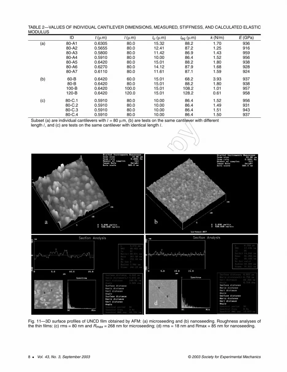
slight misalignment of the (110) wafer direction with respectto the cantilever structure defined by the photolithographicmask. The effect of this undercut requires that a calculationof an effective length be made for the cantilevers as discussedin the Data Reduction section. The undercut varied from die todie, in the range of 11–15 µm. Undercut values for individualcantilevers are given in Table 1. Figure 9(a) shows a head-onview of the end of a UNCD cantilever and Fig. 9(b) shows aclose-up of the as-etched surface. All tested cantilevers hada length of 200 µm and a width of 20 µm.
6 • Vol. 43, No. 3, September 2003 © 2003 Society for Experimental Mechanics
Proo
f Cop
y
(a)
(b)
Fig. 9—SEM image of the free end (a), and zoom to showthickness and quality of the etched surfaces (b)
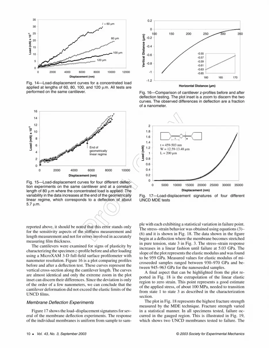
One of the most important dimensions of the cantilevers inrelation to the experiments discussed here is their thickness.We can see that when eq (1) is expressed in terms of the elasticmodulus, the film thickness becomes cubed in the denomina-tor. Small errors in this value, which is in the submicrometerregime for the tested UNCD films, can then create larger er-rors in modulus. To this end, each cantilever thickness wasindividually and carefully measured by discrete wavelengthellipsometry. Values for different cantilevers range from 0.57to 0.64 µm and are listed in Table 2.
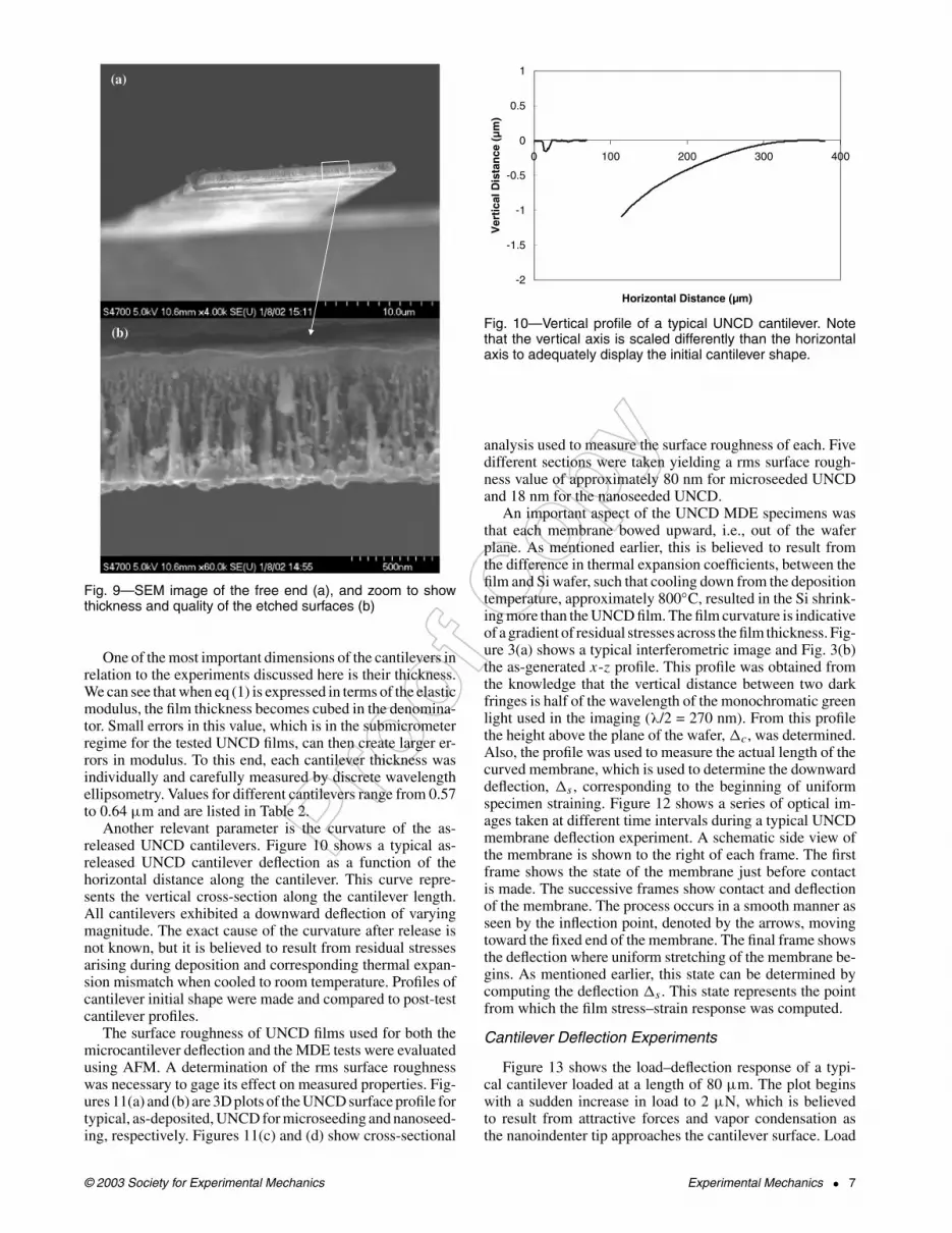
Another relevant parameter is the curvature of the as-released UNCD cantilevers. Figure 10 shows a typical as-released UNCD cantilever deflection as a function of thehorizontal distance along the cantilever. This curve repre-sents the vertical cross-section along the cantilever length.All cantilevers exhibited a downward deflection of varyingmagnitude. The exact cause of the curvature after release isnot known, but it is believed to result from residual stressesarising during deposition and corresponding thermal expan-sion mismatch when cooled to room temperature. Profiles ofcantilever initial shape were made and compared to post-testcantilever profiles.
The surface roughness of UNCD films used for both themicrocantilever deflection and the MDE tests were evaluatedusing AFM. A determination of the rms surface roughnesswas necessary to gage its effect on measured properties. Fig-ures 11(a) and (b) are 3D plots of the UNCD surface profile fortypical, as-deposited, UNCD for microseeding and nanoseed-ing, respectively. Figures 11(c) and (d) show cross-sectional
-2
-1.5
-1
-0.5
0
0.5
1
0 100 200 300 400
Horizontal Distance (µm)
Ver
tica
l Dis
tan
ce (
µm
)
Fig. 10—Vertical profile of a typical UNCD cantilever. Notethat the vertical axis is scaled differently than the horizontalaxis to adequately display the initial cantilever shape.
analysis used to measure the surface roughness of each. Fivedifferent sections were taken yielding a rms surface rough-ness value of approximately 80 nm for microseeded UNCDand 18 nm for the nanoseeded UNCD.
An important aspect of the UNCD MDE specimens wasthat each membrane bowed upward, i.e., out of the waferplane. As mentioned earlier, this is believed to result fromthe difference in thermal expansion coefficients, between thefilm and Si wafer, such that cooling down from the depositiontemperature, approximately 800◦C, resulted in the Si shrink-ing more than the UNCD film. The film curvature is indicativeof a gradient of residual stresses across the film thickness. Fig-ure 3(a) shows a typical interferometric image and Fig. 3(b)the as-generated x-z profile. This profile was obtained fromthe knowledge that the vertical distance between two darkfringes is half of the wavelength of the monochromatic greenlight used in the imaging (λ/2 = 270 nm). From this profilethe height above the plane of the wafer, ∆c, was determined.Also, the profile was used to measure the actual length of thecurved membrane, which is used to determine the downwarddeflection, ∆s , corresponding to the beginning of uniformspecimen straining. Figure 12 shows a series of optical im-ages taken at different time intervals during a typical UNCDmembrane deflection experiment. A schematic side view ofthe membrane is shown to the right of each frame. The firstframe shows the state of the membrane just before contactis made. The successive frames show contact and deflectionof the membrane. The process occurs in a smooth manner asseen by the inflection point, denoted by the arrows, movingtoward the fixed end of the membrane. The final frame showsthe deflection where uniform stretching of the membrane be-gins. As mentioned earlier, this state can be determined bycomputing the deflection ∆s . This state represents the pointfrom which the film stress–strain response was computed.
Cantilever Deflection Experiments
Figure 13 shows the load–deflection response of a typi-cal cantilever loaded at a length of 80 µm. The plot beginswith a sudden increase in load to 2 µN, which is believedto result from attractive forces and vapor condensation asthe nanoindenter tip approaches the cantilever surface. Load
© 2003 Society for Experimental Mechanics Experimental Mechanics • 7
Proo
f Cop
y
TABLE 2—VALUES OF INDIVIDUAL CANTILEVER DIMENSIONS, MEASURED, STIFFNESS, AND CALCULATED ELASTICMODULUS
ID t (µm) l (µm) lu (µm) leq (µm) k (N/m) E (GPa)(a) 80-A1 0.6305 80.0 15.32 88.2 1.70 936
80-A2 0.5655 80.0 12.41 87.2 1.25 91680-A3 0.5800 80.0 11.42 86.9 1.43 95980-A4 0.5910 80.0 10.00 86.4 1.52 95680-A5 0.6420 80.0 15.01 88.2 1.80 93880-A6 0.6270 80.0 14.12 87.9 1.68 92880-A7 0.6110 80.0 11.61 87.1 1.59 924
(b) 60-B 0.6420 60.0 15.01 68.2 3.93 93780-B 0.6420 80.0 15.01 88.2 1.80 938
100-B 0.6420 100.0 15.01 108.2 1.01 957120-B 0.6420 120.0 15.01 128.2 0.61 958
(c) 80-C.1 0.5910 80.0 10.00 86.4 1.52 95680-C.2 0.5910 80.0 10.00 86.4 1.49 93180-C.3 0.5910 80.0 10.00 86.4 1.51 94380-C.4 0.5910 80.0 10.00 86.4 1.50 937
Subset (a) are individual cantilevers with l = 80 µm, (b) are tests on the same cantilever with differentlength l, and (c) are tests on the same cantilever with identical length l.
a b
c d
Fig. 11—3D surface profiles of UNCD film obtained by AFM: (a) microseeding and (b) nanoseeding. Roughness analyses ofthe thin films: (c) rms = 80 nm and Rmax = 268 nm for microseeding; (d) rms = 18 nm and Rmax = 85 nm for nanoseeding.
8 • Vol. 43, No. 3, September 2003 © 2003 Society for Experimental Mechanics

Proo
f Cop
y
t = 0
t = 20
t = 5
t = 10
t = 15
Stress-strain curve begins at this point
t = 0
t = 20
t = 5
t = 10
t = 15
t = 0
t = 20
t = 5
t = 10
t = 15
Stress-strain curve begins at this point
Fig. 12—Optical interferometric images of the MDE specimen gauged region at five different time intervals with correspondingside-view schematic diagram showing the x-z profile of the membrane. The solid arrow denotes the position of the curvatureinflection point and the outlined arrow the position of the nanoindenter tip. Uniform straining begins at the last frame andrepresents the beginning of the computed stress-strain response.
0.0
2.0
4.0
6.0
8.0
10.0
12.0
14.0
16.0
18.0
0 2000 4000 6000 8000 10000 12000
Displacement (nm)
Lo
ad (
mN
) x1
0-3
Slope = 1.7 x 10⁻⁶
Fig. 13—Load-deflection curve for an 80 µm long cantilever.The slope, obtained from minimum square fit, represents thecantilever stiffness.
remains at this level for a period of time before increasingwith deflection in a linear manner. The extrapolation of thislinear region back to the zero-load and zero-displacementorigin indicates that this phenomenon is likely due to variousmechanisms occurring when contact is being made betweenthe two bodies.
The slope of the linear region in Fig. 13 represents the elas-tic stiffness, k, of the UNCD cantilever. Using the parametersl = 80 µm, lu = 15.32 µm, k = 1.7 N m−1, t = 0.6305 µm,and b = 20 µm for the cantilever; eq (2) provides the equiv-alent length, leq= 88.2 µm, and eq (1) the Young’s modulus,E = 937 GPa. This value is higher than the modulus mea-sured by nanoindentation, which yielded an average value of886 GPa.9 Results of stiffness for several other cantilevers are
given in Table 2. Measured values of elastic modulus for thin-film UNCD ranged from 916–959 GPa, subset (a) in Table 2.This scatter is the result of experimental errors associated tosmall inaccuracies in measuring film thickness.
Deflection tests for different cantilever lengths were alsoperformed successively on the same cantilever by applyingthe contact force at lengths of 60, 80, 100, and 120 µm.The load–displacement responses are compared in Fig. 14.Each length exhibited linear behavior after contact with thecantilever surface. The stiffness increased proportionally asthe cantilever length decreased in accordance with eq (1).The elastic modulus was calculated for each length and islisted in Table 2 as subset (b). Values of 937, 938, 957 and958 GPa were obtained for cantilever lengths of 60–120 µm,respectively. All values fall well within the range measuredin subset (a) where all cantilevers had a length of 80 µm. Al-though these results suggest a transition from lower to highermodulus between lengths of 60–80 µm and 100–120 µm, webelieve this is not a real trend but only a manifestation of thenormal scatter and experimental error of the technique. Sincethe tests were performed on the same cantilever where eachtest uses the same measured thickness, this error representsirregularities in measured stiffness and/or in the positioningof the nanoindenter tip with respect to the beam fixed support.
Deflection tests were also performed successively on thesame cantilever to examine repeatability of the technique.Figure 15 shows the load–displacement curves for four suc-cessive tests on the same cantilever. The curves and measuredstiffness match well between tests. Values of stiffness andcalculated elastic modulus are listed as subset (c) in Table 2.Stiffness varied from 1.49 to 1.52 N m−1 with correspondingvarying moduli of 931–956 GPa. These data provide confi-dence in the repeatability of the cantilever-based experimentsto yield measured stiffness and modulus values to within 2.7percent error. As with the different cantilever length tests
© 2003 Society for Experimental Mechanics Experimental Mechanics • 9
Proo
f Cop
y
0
5
10
15
20
25
30
35
0 2000 4000 6000 8000 10000 12000
Displacement (nm)
Lo
ad (
mN
) x
10-3
l = 60 µm
80 µm
100 µm
120 µm
Fig. 14—Load-displacement curves for a concentrated loadapplied at lengths of 60, 80, 100, and 120 µm. All tests areperformed on the same cantilever.
0
2
4
6
8
10
12
14
16
0 2000 4000 6000 8000 10000
Displacement (nm)
Lo
ad (
mN
) x
10-3
End ofgeometricallylinear regime
Fig. 15—Load-displacement curves for four different deflec-tion experiments on the same cantilever and at a constantlength of 80 µm where the concentrated load is applied. Thevariability in the data increases at the end of the geometricallylinear regime, which corresponds to a deflection of about5.7 µm.
reported above, it should be noted that this error stands onlyfor the sensitivity aspects of the stiffness measurement andlength measurement and not for errors involved in accuratelymeasuring film thickness.
The cantilevers were examined for signs of plasticity bycharacterizing the specimen z-profile before and after loadingusing a MicroXAM 3-D full-field surface profilometer withnanometer resolution. Figure 16 is a plot comparing profilesbefore and after a deflection test. These curves represent thevertical cross-section along the cantilever length. The curvesare almost identical and only the extreme zoom in the plotinset can discern their differences. Since the deviation is onlyof the order of a few nanometers, we can conclude that thecantilever deformation did not exceed the elastic limits of theUNCD films.
Membrane Deflection Experiments
Figure 17 shows the load–displacement signatures for sev-eral of the membrane deflection experiments. The responseof the individual membranes is uniform from sample to sam-
-1.2
-1
-0.8
-0.6
-0.4
-0.2
0
0.2
100 150 200 250 300 350
Horizontal Distance (µm)
Ver
tica
l Dis
tan
ce (
µm
)
-0.65-0.63-0.61-0.59-0.57-0.55
160 165 170
Fig. 16—Comparison of cantilever z-profiles before and afterdeflection testing. The plot inset is a zoom to discern the twocurves. The observed differences in deflection are a fractionof a nanometer.
0
0.2
0.4
0.6
0.8
1
1.2
1.4
1.6
1.8
2
0 5000 10000 15000 20000 25000 30000 35000
Displacement (nm)
Lo
ad (
mN
)
L W
t = 459-503 nmW = 12.59-13.48 µmL = 200 µm
Fig. 17—Load-displacement signatures of four differentUNCD MDE tests
ple with each exhibiting a statistical variation in failure point.The stress–strain behavior was obtained using equations (3)–(6) and it is shown in Fig. 18. The data shown in the figurebegin at a deflection where the membrane becomes stretchedin pure tension, state 3 in Fig. 3. The stress–strain responseincreases in a linear fashion until failure at 5.03 GPa. Theslope of the plot represents the elastic modulus and was foundto be 959 GPa. Measured values for elastic modulus of mi-croseeded samples ranged between 930–970 GPa and be-tween 945–963 GPa for the nanoseeded samples.
A final aspect that can be highlighted from the plot re-ported in Fig. 18 is the extrapolation of the linear elasticregion to zero strain. This point represents a good estimateof the applied stress, of about 100 MPa, needed to transitionfrom state 1 to state 3 as described in the characterizationsection.
The plot in Fig. 18 represents the highest fracture strengthmeasured by the MDE technique. Fracture strength variedin a statistical manner. In all specimens tested, failure oc-curred in the gauged region. This is illustrated in Fig. 19,which shows two UNCD membranes tested to failure. The
10 • Vol. 43, No. 3, September 2003 © 2003 Society for Experimental Mechanics

Proo
f Cop
y
0.0
1000.0
2000.0
3000.0
4000.0
5000.0
6000.0
0 0.001 0.002 0.003 0.004 0.005 0.006
Strain
Str
ess
(MP
a)
Slope = 949 GPa
σ0 ~ 100 MPa
σf = 5.03 GPa
Fig. 18—Stress-strain curve representative of a typicalUNCD MDE sample. An elastic modulus of 949 GPa, afracture stress of 5.03 GPa, and an estimated initial stress of100 MPa were identified.
upper sample has failed on the right-hand gage while thebottom sample has failed simultaneously in both gaged re-gions. Fracture strength varied from 0.89 to 2.42 GPa forthe microseeded samples and from 3.95 to 5.03 GPa for thenanoseeded samples. The variation is believed to result fromdifferences in specimen flaws generated during the seeding,deposition, and microfabrication processes. We attribute thelow fracture values of the microseeded samples to scratch-like and other defects identified on the film surface as shownin the inset of Fig. 3. We believe that these defects originatedfrom the seeding process used to grow the UNCD films andthat they affect the fracture strength more than the materialmoduli. The new nanoseeding process significantly reducedthe surface roughness and eliminated scratch-like and othersurface defects. As a result, the process not only reduced thespreading in measured elastic modulus but also more thandoubled the film fracture strength. It is expected that furtherimprovements in processing can improve fracture strength toeven higher values.
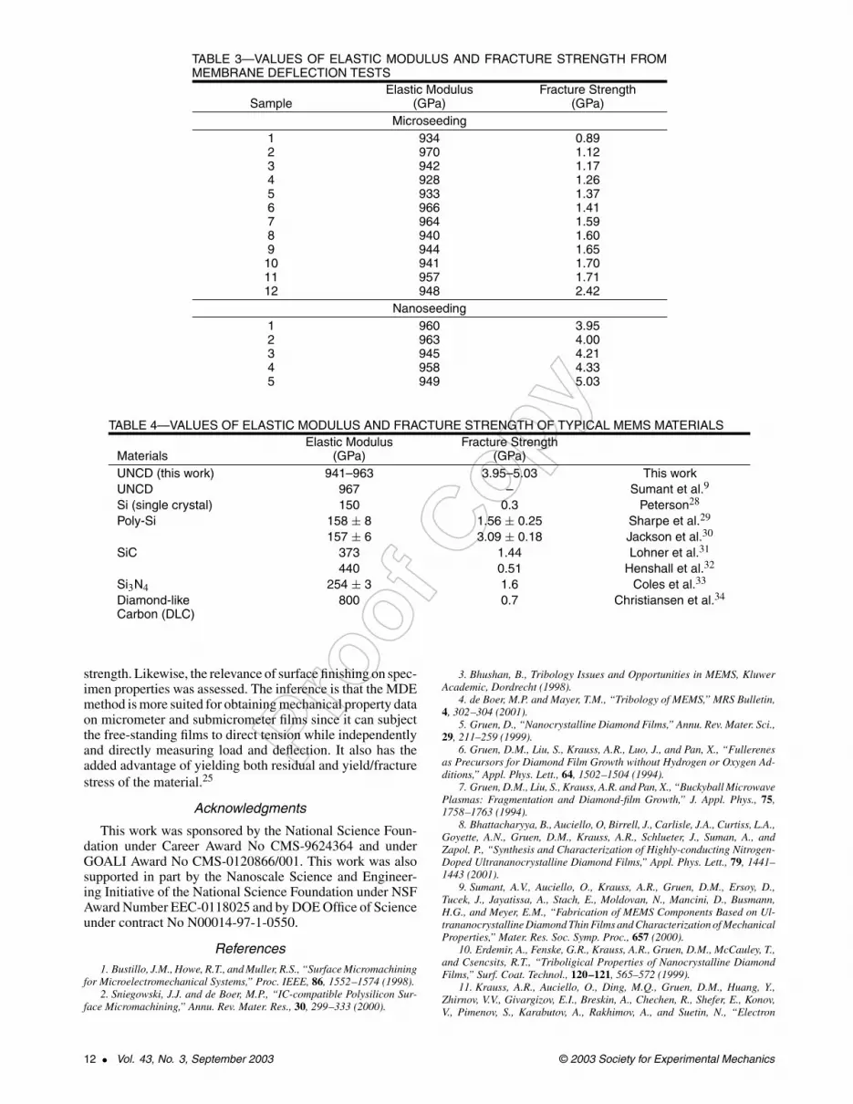
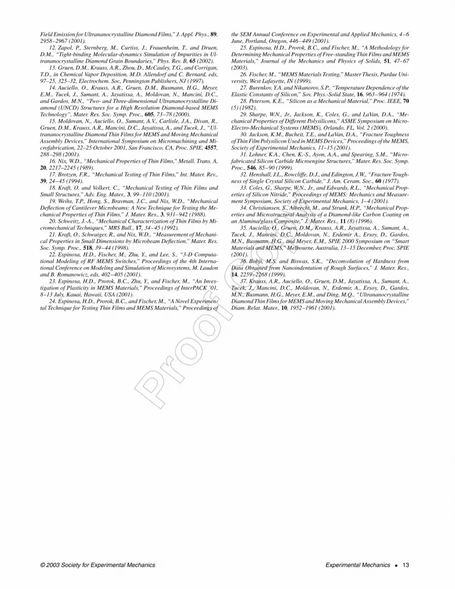
Table 3 summarizes the results on both microseeded andnanoseeded specimens tested by the MDE technique. Themeasured properties are very promising when compared toother common MEMS materials; see Table 4. The elasticmodulus is considerably higher than that for single-crystalSi, polycrystalline Si, SiC, Si3N4, or diamond-like carbon(literature references for these materials are given in Table4). The fracture strength of UNCD is also unmatched. Theresults of this work demonstrate the significant mechanicaladvantages that UNCD can provide to MEMS/NEMS de-vices. When combined with the other significant propertiesmentioned in the introduction, it is clear that UNCD is poisedto gain attention in the field.
Conclusions
In this work, microcantilever deflection and membranedeflection experiments were used to determine the elasticmodulus and strength of UNCD thin films. Values of mod-ulus ranging from 916 to 959 GPa were measured with thecantilever deflection technique. A comparison of cantilevertopography before and after deflection testing reveals iden-
Fig. 19—SEM image of two MDE specimens after testing.Both membranes show that failure occurs in the gagedregions where axial deformation is uniform.
tical shape and suggests that the elastic limit of UNCD wasnot exceeded. The largest source of error in the method wasbelieved to be accurate measurement of the film thickness,which in the modulus calculation is cubed and in the denom-inator, see eq (1). The test was also verified by deflecting asingle-crystal silicon cantilever of a common AFM tapping-mode tip. The elastic modulus measured was consistent withthe literature value of 170 GPa in the [110] direction.
Characterization of the UNCD films by the MDE yieldedelastic modulus values between 930–970 GPa for the mi-croseeded samples and between 945–963 GPa for thenanoseeded samples. These results agreed well with those ob-tained by the microcantilever-based technique and prior mea-surements using nanoindentation,9 although the MDE resultsexhibited a smaller degree of variability. The fracture strengthof the UNCD membrane varied from 0.89 to 2.42 GPa forthe microseeded samples and from 3.95 to 5.03 GPa for thenanoseeded samples. This increase is believed to result fromfewer flaws through the nanoseeding process. The out-of-plane initial shape of the MDE membranes challenged thedata reduction; however, its careful consideration in the dataprocessing allowed for an interpretation of the material re-sponse in pure tension. Future work will involve a more in-depth study of fracture behavior with specimens of a moreuniform size and with fewer and smaller flaws through bettercontrol of the wafer processing variables.
The characterization of mechanical properties of thin-film-based MEMS structures, such as those discussed in thispaper, is quite challenging because properties may dependnot only on the intrinsic microstructure or composition of thematerial but also on specific features of the film manufac-turing process. In this work, reliable data on material prop-erties were extracted by the utilization of microscale testingmethodologies. The results of both testing methods used inthe work discussed here yielded very similar elastic modu-lus values, although the cantilever deflection technique wasonly able to characterize the material’s elastic modulus andnot the strength. The MDE method proved to be more ver-satile and yielded other material properties such as fracture
© 2003 Society for Experimental Mechanics Experimental Mechanics • 11
Proo
f Cop
y
TABLE 3—VALUES OF ELASTIC MODULUS AND FRACTURE STRENGTH FROMMEMBRANE DEFLECTION TESTS
Elastic Modulus Fracture StrengthSample (GPa) (GPa)
Microseeding1 934 0.892 970 1.123 942 1.174 928 1.265 933 1.376 966 1.417 964 1.598 940 1.609 944 1.65
10 941 1.7011 957 1.7112 948 2.42
Nanoseeding1 960 3.952 963 4.003 945 4.214 958 4.335 949 5.03
TABLE 4—VALUES OF ELASTIC MODULUS AND FRACTURE STRENGTH OF TYPICAL MEMS MATERIALSElastic Modulus Fracture Strength
Materials (GPa) (GPa)UNCD (this work) 941–963 3.95–5.03 This workUNCD 967 – Sumant et al.9
Si (single crystal) 150 0.3 Peterson28
Poly-Si 158 ± 8 1.56 ± 0.25 Sharpe et al.29
157 ± 6 3.09 ± 0.18 Jackson et al.30
SiC 373 1.44 Lohner et al.31
440 0.51 Henshall et al.32
Si3N4 254 ± 3 1.6 Coles et al.33
Diamond-like 800 0.7 Christiansen et al.34
Carbon (DLC)
strength. Likewise, the relevance of surface finishing on spec-imen properties was assessed. The inference is that the MDEmethod is more suited for obtaining mechanical property dataon micrometer and submicrometer films since it can subjectthe free-standing films to direct tension while independentlyand directly measuring load and deflection. It also has theadded advantage of yielding both residual and yield/fracturestress of the material.25
Acknowledgments
This work was sponsored by the National Science Foun-dation under Career Award No CMS-9624364 and underGOALI Award No CMS-0120866/001. This work was alsosupported in part by the Nanoscale Science and Engineer-ing Initiative of the National Science Foundation under NSFAward Number EEC-0118025 and by DOE Office of Scienceunder contract No N00014-97-1-0550.
References1. Bustillo, J.M., Howe, R.T., and Muller, R.S., “Surface Micromachining
for Microelectromechanical Systems,” Proc. IEEE, 86, 1552–1574 (1998).2. Sniegowski, J.J. and de Boer, M.P., “IC-compatible Polysilicon Sur-
face Micromachining,” Annu. Rev. Mater. Res., 30, 299–333 (2000).
3. Bhushan, B., Tribology Issues and Opportunities in MEMS, KluwerAcademic, Dordrecht (1998).
4. de Boer, M.P. and Mayer, T.M., “Tribology of MEMS,” MRS Bulletin,4, 302–304 (2001).
5. Gruen, D., “Nanocrystalline Diamond Films,” Annu. Rev. Mater. Sci.,29, 211–259 (1999).
6. Gruen, D.M., Liu, S., Krauss, A.R., Luo, J., and Pan, X., “Fullerenesas Precursors for Diamond Film Growth without Hydrogen or Oxygen Ad-ditions,” Appl. Phys. Lett., 64, 1502–1504 (1994).
7. Gruen, D.M., Liu, S., Krauss, A.R. and Pan, X., “Buckyball MicrowavePlasmas: Fragmentation and Diamond-film Growth,” J. Appl. Phys., 75,1758–1763 (1994).
8. Bhattacharyya, B., Auciello, O, Birrell, J., Carlisle, J.A., Curtiss, L.A.,Goyette, A.N., Gruen, D.M., Krauss, A.R., Schlueter, J., Suman, A., andZapol, P., “Synthesis and Characterization of Highly-conducting Nitrogen-Doped Ultrananocrystalline Diamond Films,” Appl. Phys. Lett., 79, 1441–1443 (2001).
9. Sumant, A.V., Auciello, O., Krauss, A.R., Gruen, D.M., Ersoy, D.,Tucek, J., Jayatissa, A., Stach, E., Moldovan, N., Mancini, D., Busmann,H.G., and Meyer, E.M., “Fabrication of MEMS Components Based on Ul-trananocrystalline Diamond Thin Films and Characterization of MechanicalProperties,” Mater. Res. Soc. Symp. Proc., 657 (2000).
10. Erdemir, A., Fenske, G.R., Krauss, A.R., Gruen, D.M., McCauley, T.,and Csencsits, R.T., “Triboligical Properties of Nanocrystalline DiamondFilms,” Surf. Coat. Technol., 120–121, 565–572 (1999).
11. Krauss, A.R., Auciello, O., Ding, M.Q., Gruen, D.M., Huang, Y.,Zhirnov, V.V., Givargizov, E.I., Breskin, A., Chechen, R., Shefer, E., Konov,V., Pimenov, S., Karabutov, A., Rakhimov, A., and Suetin, N., “Electron
12 • Vol. 43, No. 3, September 2003 © 2003 Society for Experimental Mechanics
Proo
f Cop
y
Field Emission for Ultrananocrystalline Diamond Films,” J. Appl. Phys., 89,2958–2967 (2001).
12. Zapol, P., Sternberg, M., Curtiss, J., Frauenheim, T., and Druen,D.M., “Tight-binding Molecular-dynamics Simulation of Impurities in Ul-trananocrystalline Diamond Grain Boundaries,” Phys. Rev. B, 65 (2002).
13. Gruen, D.M., Krauss, A.R., Zhou, D., McCauley, T.G., and Corrigan,T.D., in Chemical Vapor Deposition, M.D. Allendorf and C. Bernard, eds,97–25, 325–32, Electrochem. Soc, Pennington Publishers, NJ (1997).
14. Auciello, O., Krauss, A.R., Gruen, D.M., Busmann, H.G., Meyer,E.M., Tucek, J., Sumant, A., Jayatissa, A., Moldovan, N., Mancini, D.C.,and Gardos, M.N., “Two- and Three-dimensional Ultrananocrystalline Di-amond (UNCD) Structures for a High Resolution Diamond-based MEMSTechnology”, Mater. Res. Soc. Symp. Proc., 605, 73–78 (2000).
15. Moldovan, N., Auciello, O., Sumant, A.V., Carlisle, J.A., Divan, R.,Gruen, D.M., Krauss, A.R., Mancini, D.C., Jayatissa, A., and Tucek, J., “Ul-trananocrystalline Diamond Thin Films for MEMS and Moving MechanicalAssembly Devices,” International Symposium on Micromachining and Mi-crofabrication, 22–25 October 2001, San Francisco, CA, Proc. SPIE, 4557,288–298 (2001).
16. Nix, W.D., “Mechanical Properties of Thin Films,” Metall. Trans. A,20, 2217–2245 (1989).
17. Brotzen, F.R., “Mechanical Testing of Thin Films,” Int. Mater. Rev.,39, 24–45 (1994).
18. Kraft, O. and Volkert, C., “Mechanical Testing of Thin Films andSmall Structures,” Adv. Eng. Mater., 3, 99–110 (2001).
19. Weihs, T.P., Hong, S., Bravman, J.C., and Nix, W.D., “MechanicalDeflection of Cantilever Microbeams: A New Technique for Testing the Me-chanical Properties of Thin Films,” J. Mater. Res., 3, 931–942 (1988).
20. Schweitz, J.-A., “Mechanical Characterization of Thin Films by Mi-cromechanical Techniques,” MRS Bull., 17, 34–45 (1992).
21. Kraft, O., Schwaiger, R., and Nix, W.D., “Measurement of Mechani-cal Properties in Small Dimensions by Microbeam Deflection,” Mater. Res.Soc. Symp. Proc., 518, 39–44 (1998).
22. Espinosa, H.D., Fischer, M., Zhu, Y., and Lee, S., “3-D Computa-tional Modeling of RF MEMS Switches,” Proceedings of the 4th Interna-tional Conference on Modeling and Simulation of Microsystems, M. Laudonand B. Romanowicz, eds, 402–405 (2001).
23. Espinosa, H.D., Prorok, B.C., Zhu, Y., and Fischer, M., “An Inves-tigation of Plasticity in MEMS Materials,” Proceedings of InterPACK ’01,8–13 July, Kauai, Hawaii, USA (2001).
24. Espinosa, H.D., Prorok, B.C., and Fischer, M., “A Novel Experimen-tal Technique for Testing Thin Films and MEMS Materials,” Proceedings of
the SEM Annual Conference on Experimental and Applied Mechanics, 4–6June, Portland, Oregon, 446–449 (2001).
25. Espinosa, H.D., Prorok, B.C., and Fischer, M., “A Methodology forDetermining Mechanical Properties of Free-standing Thin Films and MEMSMaterials,” Journal of the Mechanics and Physics of Solids, 51, 47–67(2003).
26. Fischer, M., “MEMS Materials Testing,” Master Thesis, Purdue Uni-versity, West Lafayette, IN (1999).
27. Burenkov, Y.A. and Nikanorov, S.P., “Temperature Dependence of theElastic Constants of Silicon,” Sov. Phys.-Solid State, 16, 963–964 (1974).
28. Peterson, K.E., “Silicon as a Mechanical Material,” Proc. IEEE, 70(5) (1982).
29. Sharpe, W.N., Jr., Jackson, K., Coles, G., and LaVan, D.A., “Me-chanical Properties of Different Polysilicons,” ASME Symposium on Micro-Electro-Mechanical Systems (MEMS), Orlando, FL, Vol. 2 (2000).
30. Jackson, K.M., Bucheit, T.E., and LaVan, D.A., “Fracture Toughnessof Thin Film Polysilicon Used in MEMS Devices,” Proceedings of the MEMS,Society of Experimental Mechanics, 11–15 (2001).
31. Lohner, K.A., Chen, K.-S., Ayon, A.A., and Spearing, S.M., “Micro-fabricated Silicon Carbide Microengine Structures,” Mater. Res. Soc. Symp.Proc., 546, 85–90 (1999).
32. Henshall, J.L., Rowcliffe, D.J., and Edington, J.W., “Fracture Tough-ness of Single Crystal Silicon Carbide,” J. Am. Ceram. Soc., 60 (1977).
33. Coles, G., Sharpe, W.N., Jr., and Edwards, R.L., “Mechanical Prop-erties of Silicon Nitride,” Proceedings of MEMS: Mechanics and Measure-ment Symposium, Society of Experimental Mechanics, 1–4 (2001).
34. Christiansen, S., Albrecht, M., and Strunk, H.P., “Mechanical Prop-erties and Microstructural Analysis of a Diamond-like Carbon Coating onan Alumina/glass Composite,” J. Mater. Res., 11 (8) (1996).
35. Auciello, O., Gruen, D.M., Krauss, A.R., Jayatissa, A., Sumant, A.,Tucek, J., Mancini, D.C., Moldovan, N., Erdemir A., Ersoy, D., Gardos,M.N., Busmann, H.G., and Meyer, E.M., SPIE 2000 Symposium on “SmartMaterials and MEMS,” Melbourne, Australia, 13–15 December, Proc. SPIE(2001).
36. Bobji, M.S. and Biswas, S.K., “Deconvolution of Hardness fromData Obtained from Nanoindentation of Rough Surfaces,” J. Mater. Res.,14, 2259–2268 (1999).
37. Krauss, A.R., Auciello, O., Gruen, D.M., Jayatissa, A., Sumant, A.,Tucek, J., Mancini, D.C., Moldovan, N., Erdemir, A., Ersoy, D., Gardos,M.N., Busmann, H.G., Meyer, E.M., and Ding, M.Q., “UltrananocrystallineDiamond Thin Films for MEMS and Moving Mechanical Assembly Devices,”Diam. Relat. Mater., 10, 1952–1961 (2001).
© 2003 Society for Experimental Mechanics Experimental Mechanics • 13
Related Documents