1/10October 2002
SEPARATE CLOCK-UP AND CLOCK-DOWN LINES
CAPABLE OF DRIVING COMMON CATHODE LEDS AND OTHER DISPLAYS DIRECTLY
ALLOWS CASCADING WITHOUT ANY EXTERNAL CIRCUITRY
MAXIMUM INPUT CURRENT OF 1 µA AT 18 V (full package-temperature range)
QUIESCENT CURRENT SPECIFIED UP TO 20V
STANDARDIZED, SYMMETRICAL OUTPUT CHARACTERISTCS
5V, 10V AND 15V PARAMETRIC RATINGS INPUT LEAKAGE CURRENT
II = 100nA (MAX) AT VDD = 18V TA = 25°C 100% TESTED FOR QUIESCENT CURRENT MEETS ALL REQUIREMENTS OF JEDEC
JESD13B "STANDARD SPECIFICATIONS FOR DESCRIPTION OF B SERIES CMOS DEVICES"
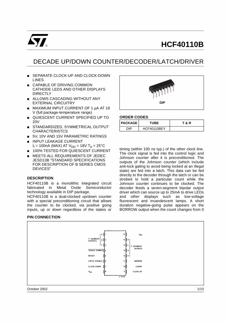
DESCRIPTIONHCF40110B is a monolithic integrated circuitfabricated in Metal Oxide Semiconductortechnology available in DIP package. HCF40110B is a dual-clocked up/down counterwith a special preconditioning circuit that allowsthe counter to be clocked, via positive goinginputs, up or down regardless of the states or
timing (within 100 ns typ.) of the other clock line.The clock signal is fed into the control logic andJohnson counter after it is preconditioned. Theoutputs of the Johnson counter (which includeanti-lock gating to avoid being locked at an illegalstate) are fed into a latch. This data can be feddirectly to the decoder through the latch or can bestrobed to hold a particular count while theJohnson counter continues to be clocked. Thedecoder feeds a seven-segment bipolar outputdriver which can source up to 25mA to drive LEDsand other displays such as low-voltagefluorescent and incandescent lamps. A shortduration negative-going pulse appears on theBORROW output when the count changes from 0
HCF40110B
DECADE UP/DOWN COUNTER/DECODER/LATCH/DRIVER
PIN CONNECTION
ORDER CODES
PACKAGE TUBE T & R
DIP HCF40110BEY
DIP
HCF40110B
2/10
to 9 or the CARRY output when the count changesfrom 9 to 0. At other times the BORROW andBORROW outputs can be tied directly to the
clock-up and clock-down lines, respectively, ofanother HCF40110B for easy cascading ofseveral counters.
INPUT EQUIVALENT CIRCUIT PIN DESCRIPTION
FUNCTIONAL DIAGRAM (One Half)
PIN No SYMBOL NAME AND FUNCTION
1, 15, 14, 13, 12, 3, 2
a, b, c, d, e, f, g
7 Segment Outputs
4Toggle Enable
Enable Johnson Counter
5 Reset Reset Input
6 Latch Enable Latch Enable
7 Clock Down Clock Down
9 Clock Up Clock Up
10 Carry Carry Output
11 Borrow Borrow Output
8 VSS Negative Supply Voltage
16 VDD Positive Supply Voltage
HCF40110B
3/10
TRUTH TABLES
X : Don’t Care* : Typically 100 ns between clock-up and clock-down positive transitions are required to ensure proper counting
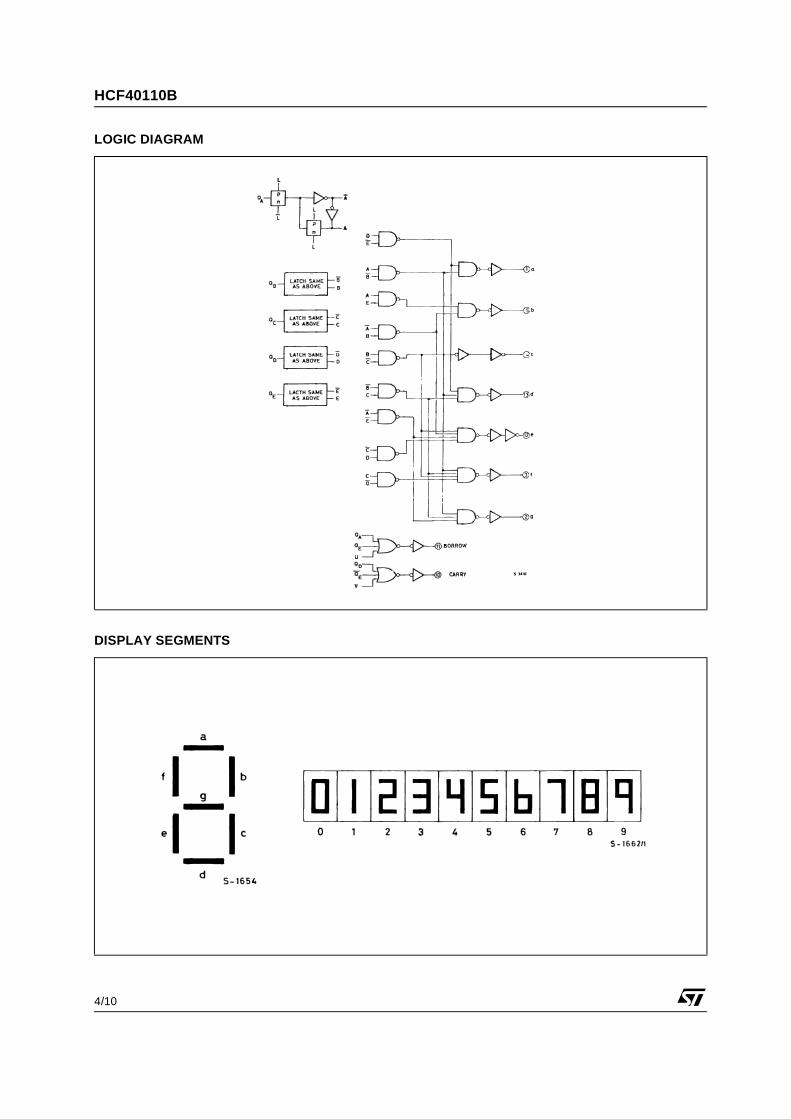
LOGIC DIAGRAM
CLOCK UP*
CLOCK DOWN*
LATCH ENABLE
TOGGLE ENABLE RESET COUNTER DISPLAY
X L L L Increments by 1 Follows Counter
X L L L Decrements by 1 Follows Counter
X X L No Change No Change
X X X X H Goes to 00000 Follow Counter (Display = 0)
X X X H L Inhibited Remains Fixed
X H L L Increments by 1 Remains Fixed
X H L L Decrements by 1 Remains Fixed
HCF40110B
4/10
LOGIC DIAGRAM
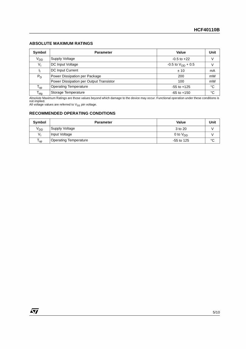
DISPLAY SEGMENTS
HCF40110B
5/10
ABSOLUTE MAXIMUM RATINGS
Absolute Maximum Ratings are those values beyond which damage to the device may occur. Functional operation under these conditions is not implied.All voltage values are referred to VSS pin voltage.
RECOMMENDED OPERATING CONDITIONS
Symbol Parameter Value Unit
VDD Supply Voltage -0.5 to +22 V
VI DC Input Voltage -0.5 to VDD + 0.5 V
II DC Input Current ± 10 mA
PD Power Dissipation per Package 200 mW
Power Dissipation per Output Transistor 100 mW
Top Operating Temperature -55 to +125 °C
Tstg Storage Temperature -65 to +150 °C
Symbol Parameter Value Unit
VDD Supply Voltage 3 to 20 V
VI Input Voltage 0 to VDD V
Top Operating Temperature -55 to 125 °C
HCF40110B
6/10
DC SPECIFICATIONS
The Noise Margin for both "1" and "0" level is: 1V min. with VDD=5V, 2V min. with VDD=10V, 2.5V min. with VDD=15V
Symbol Parameter
Test Condition Value
UnitVI(V)
VO(V)
|IO|(µA)
VDD(V)
TA = 25°C -40 to 85°C -55 to 125°C
Min. Typ. Max. Min. Max. Min. Max.
IL Quiescent Current 0/5 5 0.04 5 150 150
µA0/10 10 0.04 10 300 300
0/15 15 0.04 20 600 600
0/20 20 0.08 100 3000 3000
VOH High Level Output Voltage
0/5 <1 5 4.95 4.95 4.95
V0/10 <1 10 9.95 9.95 9.95
0/15 <1 15 14.95 14.95 14.95
VOL Low Level Output Voltage
5/0 <1 5 0.05 0.05 0.05
V10/0 <1 10 0.05 0.05 0.05
15/0 <1 15 0.05 0.05 0.05
VIH High Level Input Voltage
0.5/4.5 <1 5 3.5 3.5 3.5
V1/9 <1 10 7 7 7
1.5/13.5 <1 15 11 11 11
VIL Low Level Input Voltage
4.5/0.5 <1 5 1.5 1.5 1.5
V9/1 <1 10 3 3 3
13.5/1.5 <1 15 4 4 4
IOH Output Drive Current
0/5 2.5 <1 5 -1.36 -3.2 -1.1 -1.1
mA0/5 4.6 <1 5 -0.44 -1 -0.36 -0.36
0/10 9.5 <1 10 -1.1 -2.6 -0.9 -0.9
0/15 13.5 <1 15 -3.0 -6.8 -2.4 -2.4
IOL Output Sink Current Q
0/5 0.4 <1 5 1.74 4 1.43 1.43
mA0/10 0.5 <1 10 4.42 10.4 3.74 3.74
0/15 1.5 <1 15 11.56 27.2 9.52 9.52
IOL Output Sink Current
0/5 0.4 <1 5 0.44 1 0.36 0.36
mA0/10 0.5 <1 10 1.1 2.6 0.9 0.9
0/15 1.5 <1 15 3.0 6.8 2.4 2.4
II Input Leakage Current
0/18 Any Input 18 ±10-5 ±0.1 ±1 ±1 µA
IOZ 3-State Output Leakage Current
0/18 Any Input 18 ±10-4 ±0.4 ±12 ±12 µA
CI Input Capacitance Any Input 5 7.5 pF
HCF40110B
7/10
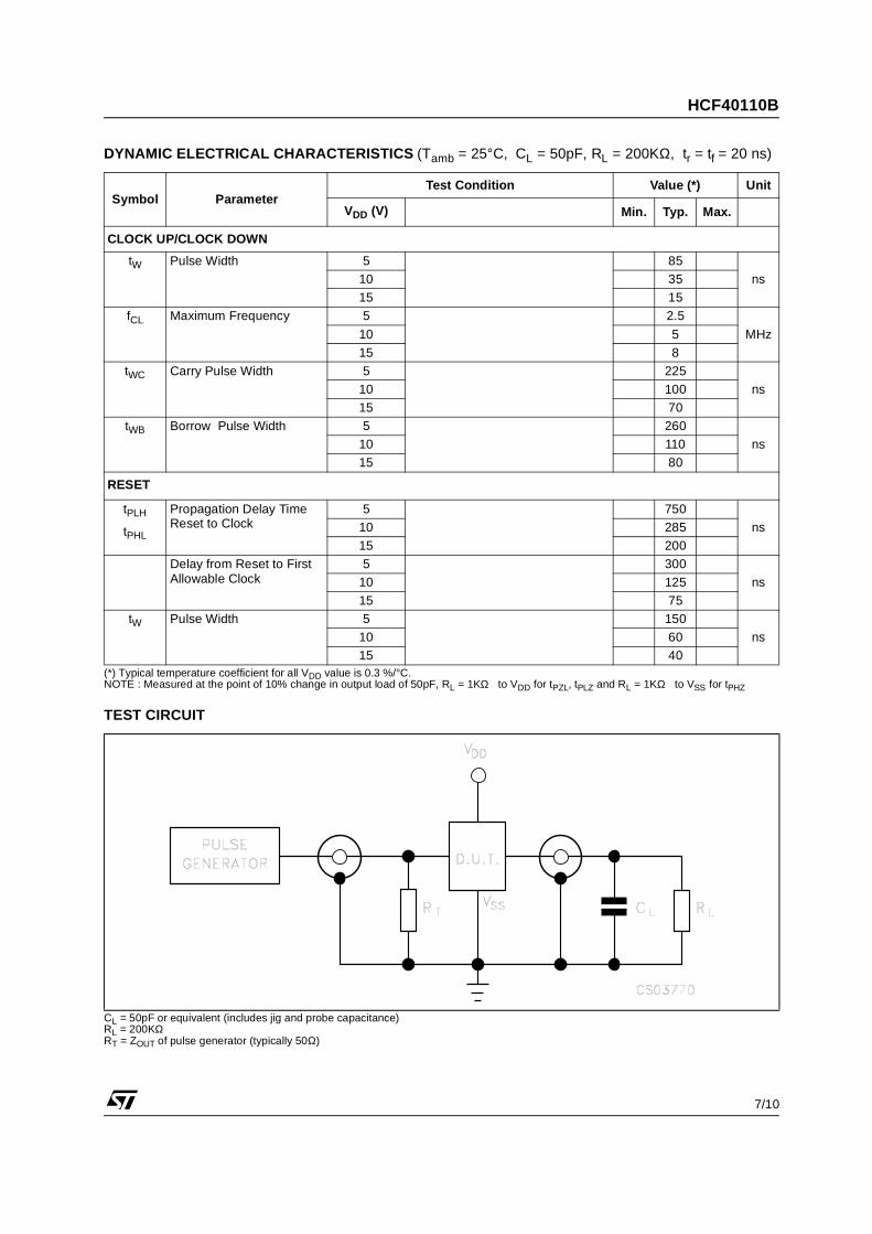
DYNAMIC ELECTRICAL CHARACTERISTICS (Tamb = 25°C, CL = 50pF, RL = 200KΩ, tr = tf = 20 ns)
(*) Typical temperature coefficient for all VDD value is 0.3 %/°C.NOTE : Measured at the point of 10% change in output load of 50pF, RL = 1KΩ to VDD for tPZL, tPLZ and RL = 1KΩ to VSS for tPHZ
TEST CIRCUIT
CL = 50pF or equivalent (includes jig and probe capacitance)RL = 200KΩRT = ZOUT of pulse generator (typically 50Ω)
Symbol ParameterTest Condition Value (*) Unit
VDD (V) Min. Typ. Max.
CLOCK UP/CLOCK DOWN
tW Pulse Width 5 85
ns10 35
15 15
fCL Maximum Frequency 5 2.5
MHz10 5
15 8
tWC Carry Pulse Width 5 225
ns10 100
15 70
tWB Borrow Pulse Width 5 260
ns10 110
15 80
RESET
tPLH
tPHL
Propagation Delay Time Reset to Clock
5 750
ns10 285
15 200
Delay from Reset to First Allowable Clock
5 300
ns10 125
15 75
tW Pulse Width 5 150
ns10 60
15 40
HCF40110B
8/10
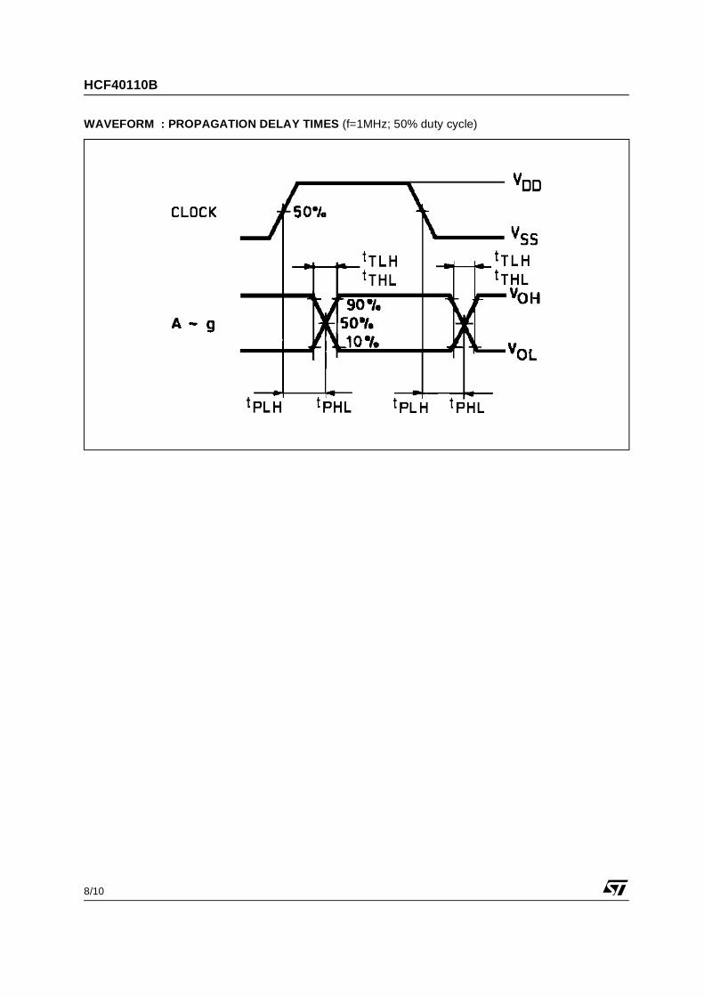
WAVEFORM : PROPAGATION DELAY TIMES (f=1MHz; 50% duty cycle)
HCF40110B
9/10
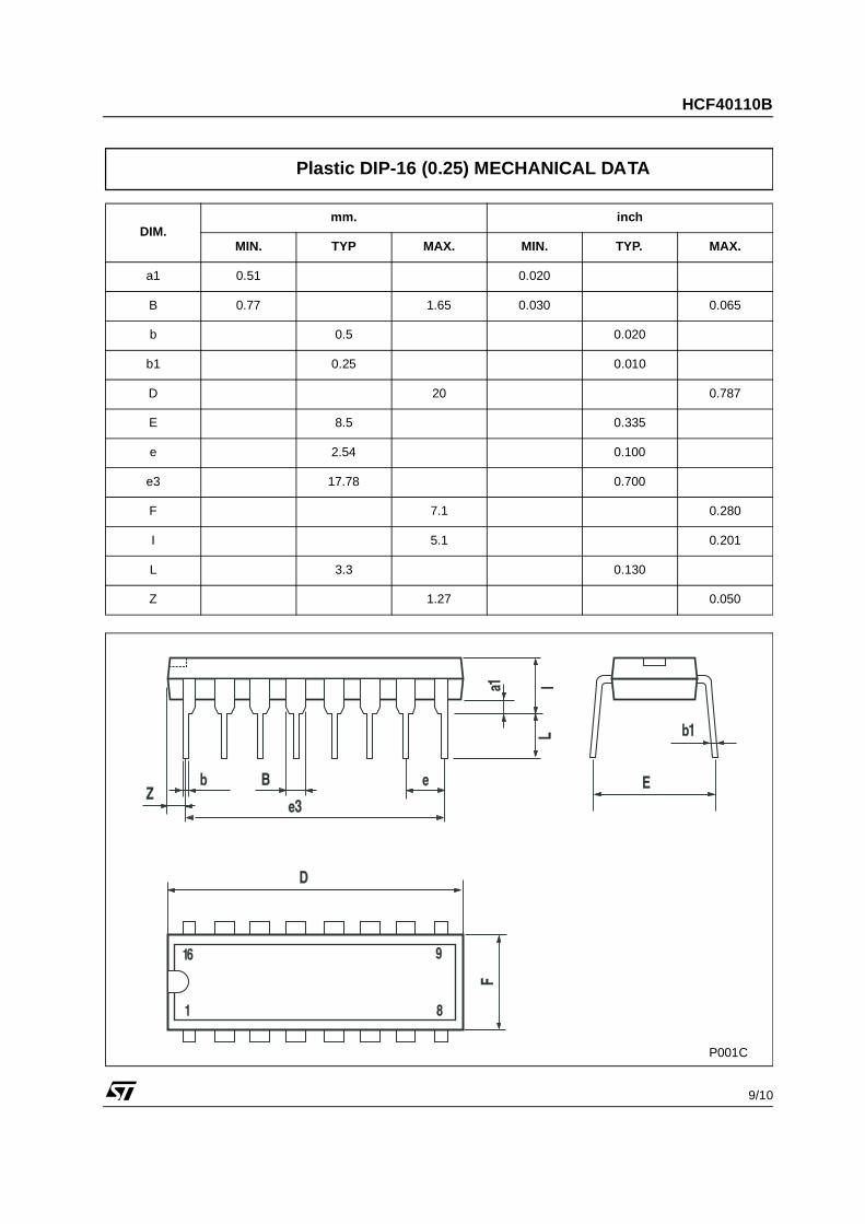
DIM.mm. inch
MIN. TYP MAX. MIN. TYP. MAX.
a1 0.51 0.020
B 0.77 1.65 0.030 0.065
b 0.5 0.020
b1 0.25 0.010
D 20 0.787
E 8.5 0.335
e 2.54 0.100
e3 17.78 0.700
F 7.1 0.280
I 5.1 0.201
L 3.3 0.130
Z 1.27 0.050
Plastic DIP-16 (0.25) MECHANICAL DATA
P001C
HCF40110B
10/10
Information furnished is believed to be accurate and reliable. However, STMicroelectronics assumes no res ponsibility for theconsequences of use of such information nor for any infringement of patents or other rights of third parties which may result f romits use. No license is granted by implication or otherwise under any patent or patent rights of STMicroelectronics. Specificati onsmentioned in this publication are subject to change without notice. This publication supersedes and replaces all informationpreviously supplied. STMicroelectronics products are not authorized for use as critical components in life support devi ces orsystems without express written approval of STMicroelectronics.
© The ST logo is a registered trademark of STMicroelectronics
© 2002 STMicroelectronics - Printed in Italy - All Rights ReservedSTMicroelectronics GROUP OF COMPANIES
Australia - Brazil - Canada - China - Finland - France - Germany - Hong Kong - India - Israel - Italy - Japan - Malaysia - Malta - Morocco Singapore - Spain - Sweden - Switzerland - United Kingdom - United States.
© http://www.st.com
Mouser Electronics
Authorized Distributor
Click to View Pricing, Inventory, Delivery & Lifecycle Information: STMicroelectronics:
HCF40110BEY