High Voltage Latch-Up Proof, 4-/8-Channel Multiplexers
Data Sheet ADG5408/ADG5409
Rev. C Document Feedback Information furnished by Analog Devices is believed to be accurate and reliable. However, no responsibility is assumed by Analog Devices for its use, nor for any infringements of patents or other rights of third parties that may result from its use. Specifications subject to change without notice. No license is granted by implication or otherwise under any patent or patent rights of Analog Devices. Trademarks and registered trademarks are the property of their respective owners.
One Technology Way, P.O. Box 9106, Norwood, MA 02062-9106, U.S.A. Tel: 781.329.4700 ©2010–2013 Analog Devices, Inc. All rights reserved. Technical Support www.analog.com
FEATURES Latch-up proof 8 kV human body model (HBM) ESD rating Low on resistance (13.5 Ω) ±9 V to ±22 V dual-supply operation 9 V to 40 V single-supply operation 48 V supply maximum ratings Fully specified at ±15 V, ±20 V, +12 V, and +36 V VSS to VDD analog signal range
APPLICATIONS Relay replacement Automatic test equipment Data acquisition Instrumentation Avionics Audio and video switching Communication systems
FUNCTIONAL BLOCK DIAGRAMS
ADG5408
S1
S8
D
ADG5409
S1A
S4B
DA
DB
S4A
S1B
1-OF-4DECODER
1-OF-8DECODER
A0 A1 ENA0 A1 A2 EN 0920
6-00
1
Figure 1.
GENERAL DESCRIPTION The ADG5408/ADG5409 are monolithic CMOS analog multi-plexers comprising eight single channels and four differential channels, respectively. The ADG5408 switches one of eight inputs to a common output, as determined by the 3-bit binary address lines, A0, A1, and A2. The ADG5409 switches one of four differential inputs to a common differential output, as determined by the 2-bit binary address lines, A0 and A1.
An EN input on both devices enables or disables the device. When EN is disabled, all channels switch off. The on-resistance profile is very flat over the full analog input range, which ensures good linearity and low distortion when switching audio signals. High switching speed also makes the parts suitable for video signal switching.
Each switch conducts equally well in both directions when on, and each switch has an input signal range that extends to the power supplies. In the off condition, signal levels up to the supplies are blocked.
The ADG5408/ADG5409 do not have VL pins; rather, the logic power supply is generated internally by an on-chip voltage generator.
PRODUCT HIGHLIGHTS 1. Trench isolation guards against latch-up. A dielectric trench
separates the P and N channel transistors thereby preventing latch-up even under severe overvoltage conditions.
2. Low RON. 3. Dual-supply operation. For applications where the analog
signal is bipolar, the ADG5408/ADG5409 can be operated from dual supplies up to ±22 V.
4. Single-supply operation. For applications where the analog signal is unipolar, the ADG5408/ADG5409 can be operated from a single rail power supply up to 40 V.
5. 3 V logic compatible digital inputs: VINH = 2.0 V, VINL = 0.8 V. 6. No VL logic power supply required.

ADG5408/ADG5409 Data Sheet
Rev. C | Page 2 of 24
TABLE OF CONTENTS Features .............................................................................................. 1 Applications ....................................................................................... 1 Functional Block Diagrams ............................................................. 1 General Description ......................................................................... 1 Product Highlights ........................................................................... 1
Revision History ........................................................................... 2 Specifications ..................................................................................... 3
±15 V Dual Supply ....................................................................... 3 ±20 V Dual Supply ....................................................................... 4 12 V Single Supply ........................................................................ 5 36 V Single Supply ........................................................................ 6 Continuous Current per Channel, Sx or D ............................... 8
Absolute Maximum Ratings ............................................................9 ESD Caution...................................................................................9
Pin Configurations and Function Descriptions ......................... 10 Typical Performance Characteristics ........................................... 12 Test Circuits ..................................................................................... 16 Terminology .................................................................................... 18 Trench Isolation .............................................................................. 19 Applications Information .............................................................. 20 Outline Dimensions ....................................................................... 21
Ordering Guide .......................................................................... 22
REVISION HISTORY 3/13—Rev. B to Rev. C
Changes to Table 5 and Table 6 ....................................................... 8 Changed ADG5408 Peak Current from 370 mA to 435 mA; Changed ADG5409 Peak Current from 275 mA to 300 mA; Changed Reflow Soldering Peak Temperature, Pb Free from 260(+0/−5)°C to As per JEDEC J-STD-020; Table 7 ................... 9 Changes to Figure 25, Figure 26, and Figure 29 ......................... 16
5/12—Rev. A to Rev. B
Removed Automotive Information (Throughout)....................... 1 Changes to Ordering Guide .......................................................... 22 Deleted Automotive Products Section ......................................... 22
6/11—Rev. 0 to Rev. A
Change to Features Section ............................................................. 1 Change to ISS Parameter, Table 2 ..................................................... 5 Changes to Figure 3 ........................................................................ 10 Changes to Figure 5 ........................................................................ 11 Updated Outline Dimensions ....................................................... 21 Changes to Ordering Guide .......................................................... 21 Added Automotive Products Section........................................... 21
7/10—Revision 0: Initial Version

Data Sheet ADG5408/ADG5409
Rev. C | Page 3 of 24
SPECIFICATIONS ±15 V DUAL SUPPLY VDD = +15 V ± 10%, VSS = −15 V ± 10%, GND = 0 V, unless otherwise noted.
Table 1. Parameter 25°C −40°C to +85°C −40°C to +125°C Unit Test Conditions/Comments ANALOG SWITCH
Analog Signal Range VDD to VSS V On Resistance, RON 13.5 Ω typ VS = ±10 V, IS = −10 mA; see Figure 26 15 18 22 Ω max VDD = +13.5 V, VSS = −13.5 V On-Resistance Match Between
Channels, ∆RON 0.3 Ω typ VS = ±10 V, IS = −10 mA
0.8 1.3 1.4 Ω max On-Resistance Flatness, RFLAT (ON) 1.8 Ω typ VS = ±10 V, IS = −10 mA 2.2 2.6 3 Ω max
LEAKAGE CURRENTS VDD = +16.5 V, VSS = −16.5 V Source Off Leakage, IS (Off ) ±0.05 nA typ VS = ±10 V, VD = 10 V; see Figure 29 ±0.25 ±1 ±7 nA max Drain Off Leakage, ID (Off ) ±0.1 nA typ VS = ±10 V, VD = 10 V; see Figure 29 ±0.4 ±4 ±30 nA max Channel On Leakage, ID (On), IS (On) ±0.1 nA typ VS = VD = ±10 V; see Figure 25 ±0.4 ±4 ±30 nA max
DIGITAL INPUTS
Input High Voltage, VINH 2.0 V min Input Low Voltage, VINL 0.8 V max Input Current, IINL or IINH 0.002 µA typ VIN = VGND or VDD ±0.1 µA max Digital Input Capacitance, CIN 3 pF typ
DYNAMIC CHARACTERISTICS1 Transition Time, tTRANSITION 170 ns typ RL = 300 Ω, CL = 35 pF 217 258 292 ns max VS = 10 V; see Figure 32 tON (EN) 140 ns typ RL = 300 Ω, CL = 35 pF 175 213 242 ns max VS = 10 V; see Figure 34 tOFF (EN) 130 ns typ RL = 300 Ω, CL = 35 pF 161 183 198 ns max VS = 10 V; see Figure 34 Break-Before-Make Time Delay, tD 50 ns typ RL = 300 Ω, CL = 35 pF
16 ns min VS1 = VS2 = 10 V; see Figure 33 Charge Injection, QINJ 115 pC typ VS = 0 V, RS = 0 Ω, CL = 1 nF;
see Figure 35 Off Isolation −60 dB typ RL = 50 Ω, CL = 5 pF, f = 1 MHz; see
Figure 28 Channel-to-Channel Crosstalk −60 dB typ RL = 50 Ω, CL = 5 pF, f = 1 MHz; see
Figure 27 Total Harmonic Distortion + Noise 0.01 % typ RL = 1 kΩ, 15 V p-p, f = 20 Hz to 20 kHz;
see Figure 30 −3 dB Bandwidth RL = 50 Ω, CL = 5 pF; see Figure 31
ADG5408 50 MHz typ ADG5409 87 MHz typ
Insertion Loss 0.9 dB typ RL = 50 Ω, CL = 5 pF, f = 1 MHz; Figure 31
CS (Off ) 15 pF typ VS = 0 V, f = 1 MHz CD (Off )
ADG5408 102 pF typ VS = 0 V, f = 1 MHz ADG5409 50 pF typ VS = 0 V, f = 1 MHz

ADG5408/ADG5409 Data Sheet
Rev. C | Page 4 of 24
Parameter 25°C −40°C to +85°C −40°C to +125°C Unit Test Conditions/Comments CD (On), CS (On)
ADG5408 133 pF typ VS = 0 V, f = 1 MHz ADG5409 81 pF typ VS = 0 V, f = 1 MHz
POWER REQUIREMENTS VDD = +16.5 V, VSS = −16.5 V IDD 45 µA typ Digital inputs = 0 V or VDD
55 70 µA max ISS 0.001 µA typ Digital inputs = 0 V or VDD
1 µA max VDD/VSS ±9/±22 V min/V max GND = 0 V
1 Guaranteed by design; not subject to production test.
±20 V DUAL SUPPLY VDD = +20 V ± 10%, VSS = −20 V ± 10%, GND = 0 V, unless otherwise noted.
Table 2. Parameter 25°C −40°C to +85°C −40°C to +125°C Unit Test Conditions/Comments ANALOG SWITCH
Analog Signal Range VDD to VSS V On Resistance, RON 12.5 Ω typ VS = ±15 V, IS = −10 mA; see Figure 26 14 17 21 Ω max VDD = +18 V, VSS = −18 V On-Resistance Match Between
Channels, ∆RON 0.3 Ω typ VS = ±15 V, IS = −10 mA
0.8 1.3 1.4 Ω max On-Resistance Flatness, RFLAT (ON) 2.3 Ω typ VS = ±15 V, IS = −10 mA 2.7 3.1 3.5 Ω max
LEAKAGE CURRENTS VDD = +22 V, VSS = −22 V Source Off Leakage, IS (Off ) ±0.1 nA typ VS = ±15 V, VD = 15 V; see Figure 29 ±0.25 ±1 ±7 nA max Drain Off Leakage, ID (Off ) ±0.15 nA typ VS = ±15 V, VD = 15 V; see Figure 29 ±0.4 ±4 ±30 nA max Channel On Leakage, ID (On), IS (On) ±0.15 nA typ VS = VD = ±15 V; see Figure 25 ±0.4 ±4 ±30 nA max
DIGITAL INPUTS Input High Voltage, VINH 2.0 V min Input Low Voltage, VINL 0.8 V max Input Current, IINL or IINH 0.002 µA typ VIN = VGND or VDD ±0.1 µA max Digital Input Capacitance, CIN 3 pF typ
DYNAMIC CHARACTERISTICS1 Transition Time, tTRANSITION 160 ns typ RL = 300 Ω, CL = 35 pF 207 237 262 ns max VS = 10 V; see Figure 32 tON (EN) 140 ns typ RL = 300 Ω, CL = 35 pF 165 194 218 ns max VS = 10 V; see Figure 34 tOFF (EN) 133 ns typ RL = 300 Ω, CL = 35 pF 153 174 189 ns max VS = 10 V; see Figure 34 Break-Before-Make Time Delay, tD 38 ns typ RL = 300 Ω, CL = 35 pF
11 ns min VS1 = VS2 = 10 V; see Figure 33 Charge Injection, QINJ 155 pC typ VS = 0 V, RS = 0 Ω, CL = 1 nF; see
Figure 35 Off Isolation −60 dB typ RL = 50 Ω, CL = 5 pF, f = 1 MHz; see
Figure 28 Channel-to-Channel Crosstalk −60 dB typ RL = 50 Ω, CL = 5 pF, f = 1 MHz;
see Figure 27

Data Sheet ADG5408/ADG5409
Rev. C | Page 5 of 24
Parameter 25°C −40°C to +85°C −40°C to +125°C Unit Test Conditions/Comments Total Harmonic Distortion + Noise 0.012 % typ RL = 1 kΩ, 20 V p-p, f = 20 Hz to 20 kHz;
see Figure 30 −3 dB Bandwidth RL = 50 Ω, CL = 5 pF; see Figure 31
ADG5408 50 MHz typ ADG5409 88 MHz typ
Insertion Loss 0.8 dB typ RL = 50 Ω, CL = 5 pF, f = 1 MHz; see Figure 31
CS (Off ) 17 pF typ VS = 0 V, f = 1 MHz CD (Off )
ADG5408 98 pF typ VS = 0 V, f = 1 MHz ADG5409 48 pF typ VS = 0 V, f = 1 MHz
CD (On), CS (On) ADG5408 128 pF typ VS = 0 V, f = 1 MHz ADG5409 80 pF typ VS = 0 V, f = 1 MHz
POWER REQUIREMENTS VDD = +22 V, VSS = −22 V IDD 50 µA typ Digital inputs = 0 V or VDD
70 110 µA max ISS 0.001 µA typ Digital inputs = 0 V or VDD 1 µA max VDD/VSS ±9/±22 V min/V max GND = 0 V
1 Guaranteed by design; not subject to production test.
12 V SINGLE SUPPLY VDD = 12 V ± 10%, VSS = 0 V, GND = 0 V, unless otherwise noted.
Table 3. Parameter 25°C −40°C to +85°C −40°C to +125°C Unit Test Conditions/Comments ANALOG SWITCH
Analog Signal Range 0 V to VDD V On Resistance, RON 26 Ω typ VS = 0 V to 10 V, IS = −10 mA; see
Figure 26 30 36 42 Ω max VDD = 10.8 V, VSS = 0 V On-Resistance Match Between
Channels, ∆RON 0.3 Ω typ VS = 0 V to 10 V, IS = −10 mA
1 1.5 1.6 Ω max On-Resistance Flatness, RFLAT (ON) 5.5 Ω typ VS = 0 V to 10 V, IS = −10 mA 6.5 8 12 Ω max
LEAKAGE CURRENTS VDD = 13.2 V, VSS = 0 V Source Off Leakage, IS (Off ) ±0.02 nA typ VS = 1 V/10 V, VD = 10 V/1 V; see
Figure 29 ±0.25 ±1 ±7 nA max Drain Off Leakage, ID (Off ) ±0.05 nA typ VS = 1 V/10 V, VD = 10 V/1 V; see
Figure 29 ±0.4 ±4 ±30 nA max Channel On Leakage, ID (On), IS (On) ±0.05 nA typ VS = VD = 1 V/10 V; see Figure 25 ±0.4 ±4 ±30 nA max
DIGITAL INPUTS Input High Voltage, VINH 2.0 V min Input Low Voltage, VINL 0.8 V max Input Current, IINL or IINH 0.002 µA typ VIN = VGND or VDD ±0.1 µA max Digital Input Capacitance, CIN 3 pF typ

ADG5408/ADG5409 Data Sheet
Rev. C | Page 6 of 24
Parameter 25°C −40°C to +85°C −40°C to +125°C Unit Test Conditions/Comments DYNAMIC CHARACTERISTICS1
Transition Time, tTRANSITION 230 ns typ RL = 300 Ω, CL = 35 pF 321 388 430 ns max VS = 8 V; see Figure 32 tON (EN) 215 ns typ RL = 300 Ω, CL = 35 pF 276 345 397 ns max VS = 8 V; see Figure 34 tOFF (EN) 134 ns typ RL = 300 Ω, CL = 35 pF 161 187 209 ns max VS = 8 V; see Figure 34 Break-Before-Make Time Delay, tD 118 ns typ RL = 300 Ω, CL = 35 pF
55 ns min VS1 = VS2 = 8 V; see Figure 33 Charge Injection, QINJ 45 pC typ VS = 6 V, RS = 0 Ω, CL = 1 nF; see
Figure 35 Off Isolation −60 dB typ RL = 50 Ω, CL = 5 pF, f = 1 MHz;
see Figure 28 Channel-to-Channel Crosstalk −60 dB typ RL = 50 Ω, CL = 5 pF, f = 1 MHz;
see Figure 27 Total Harmonic Distortion + Noise 0.1 % typ RL = 1 kΩ, 6 V p-p, f = 20 Hz to 20 kHz;
see Figure 30 −3 dB Bandwidth RL = 50 Ω, CL = 5 pF; see Figure 31
ADG5408 35 MHz typ ADG5409 74 MHz typ
Insertion Loss −1.8 dB typ RL = 50 Ω, CL = 5 pF, f = 1 MHz; see Figure 31
CS (Off ) 22 pF typ VS = 6 V, f = 1 MHz CD (Off )
ADG5408 119 pF typ VS = 6 V, f = 1 MHz ADG5409 59 pF typ VS = 6 V, f = 1 MHz
CD (On), CS (On) ADG5408 146 pF typ VS = 6 V, f = 1 MHz ADG5409 86 pF typ VS = 6 V, f = 1 MHz
POWER REQUIREMENTS VDD = 13.2 V IDD 40 µA typ Digital inputs = 0 V or VDD
50 65 µA max VDD 9/40 V min/V max GND = 0 V, VSS = 0 V
1 Guaranteed by design; not subject to production test.
36 V SINGLE SUPPLY VDD = 36 V ± 10%, VSS = 0 V, GND = 0 V, unless otherwise noted.
Table 4. Parameter 25°C −40°C to +85°C −40°C to +125°C Unit Test Conditions/Comments ANALOG SWITCH
Analog Signal Range 0 V to VDD V On Resistance, RON 14.5 Ω typ VS = 0 V to 30 V, IS = −10 mA; see
Figure 26 16 19 23 Ω max VDD = 32.4 V, VSS = 0 V On-Resistance Match Between
Channels, ∆RON 0.3 Ω typ VS = 0 V to 30 V, IS = −10 mA
0.8 1.3 1.4 Ω max On-Resistance Flatness, RFLAT (ON) 3.5 Ω typ VS = 0 V to 30 V, IS = −10 mA 4.3 5.5 6.5 Ω max
LEAKAGE CURRENTS VDD =39.6 V, VSS = 0 V Source Off Leakage, IS (Off ) ±0.1 nA typ VS = 1 V/30 V, VD = 30 V/1 V; see
Figure 29 ±0.25 ±1 ±7 nA max

Data Sheet ADG5408/ADG5409
Rev. C | Page 7 of 24
Parameter 25°C −40°C to +85°C −40°C to +125°C Unit Test Conditions/Comments Drain Off Leakage, ID (Off ) ±0.15 nA typ VS = 1 V/30 V, VD = 30 V/1 V; see
Figure 29 ±0.4 ±4 ±30 nA max Channel On Leakage, ID (On), IS (On) ±0.15 nA typ VS = VD = 1 V/30 V; see Figure 25 ±0.4 ±4 ±30 nA max
DIGITAL INPUTS Input High Voltage, VINH 2.0 V min Input Low Voltage, VINL 0.8 V max Input Current, IINL or IINH 0.002 µA typ VIN = VGND or VDD ±0.1 µA max Digital Input Capacitance, CIN 3 pF typ
DYNAMIC CHARACTERISTICS1 Transition Time, tTRANSITION 187 ns typ RL = 300 Ω, CL = 35 pF 242 257 281 ns max VS = 18 V; see Figure 32 tON (EN) 160 ns typ RL = 300 Ω, CL = 35 pF 195 219 237 ns max VS = 18 V; see Figure 34 tOFF (EN) 147 ns typ RL = 300 Ω, CL = 35 pF 184 184 190 ns max VS = 18 V; see Figure 34 Break-Before-Make Time Delay, tD 53 ns typ RL = 300 Ω, CL = 35 pF
17 ns min VS1 = VS2 = 18 V; see Figure 33 Charge Injection, QINJ 150 pC typ VS = 18 V, RS = 0 Ω, CL = 1 nF;
see Figure 35 Off Isolation −60 dB typ RL = 50 Ω, CL = 5 pF, f = 1 MHz;
see Figure 28 Channel-to-Channel Crosstalk −60 dB typ RL = 50 Ω, CL = 5 pF, f = 1 MHz;
see Figure 27 Total Harmonic Distortion + Noise 0.4 % typ RL = 1 kΩ, 18 V p-p, f = 20 Hz to 20 kHz;
see Figure 30 −3 dB Bandwidth RL = 50 Ω, CL = 5 pF; see Figure 31
ADG5408 45 MHz typ ADG5409 76 MHz typ
Insertion Loss −1 dB typ RL = 50 Ω, CL = 5 pF, f = 1 MHz; see Figure 31
CS (Off ) 18 pF typ VS = 18 V, f = 1 MHz CD (Off )
ADG5408 120 pF typ VS = 18 V, f = 1 MHz ADG5409 60 pF typ VS = 18 V, f = 1 MHz
CD (On), CS (On) ADG5408 137 pF typ VS = 18 V, f = 1 MHz ADG5409 80 pF typ VS = 18 V, f = 1 MHz
POWER REQUIREMENTS VDD = 39.6 V IDD 80 µA typ Digital inputs = 0 V or VDD
100 130 µA max VDD 9/40 V min/V max GND = 0 V, VSS = 0 V
1 Guaranteed by design; not subject to production test.

ADG5408/ADG5409 Data Sheet
Rev. C | Page 8 of 24
CONTINUOUS CURRENT PER CHANNEL, Sx OR D
Table 5. ADG5408 Parameter 25°C 85°C 125°C Unit CONTINUOUS CURRENT, Sx OR D
VDD = +15 V, VSS = −15 V TSSOP (θJA = 112.6°C/W) 120 78 50 mA maximum LFCSP (θJA = 30.4°C/W) 207 113 60 mA maximum
VDD = +20 V, VSS = −20 V TSSOP (θJA = 112.6°C/W) 127 81 51 mA maximum LFCSP (θJA = 30.4°C/W) 218 117 61 mA maximum
VDD = 12 V, VSS = 0 V TSSOP (θJA = 112.6°C/W) 97 66 44 mA maximum LFCSP (θJA = 30.4°C/W) 168 99 57 mA maximum
VDD = 36 V, VSS = 0 V TSSOP (θJA = 112.6°C/W) 125 80 50 mA maximum LFCSP (θJA = 30.4°C/W) 214 116 61 mA maximum
Table 6. ADG5409 Parameter 25°C 85°C 125°C Unit CONTINUOUS CURRENT, Sx OR D
VDD = +15 V, VSS = −15 V TSSOP (θJA = 112.6°C/W) 90 62 43 mA maximum LFCSP (θJA = 30.4°C/W) 156 95 55 mA maximum
VDD = +20 V, VSS = −20 V TSSOP (θJA = 112.6°C/W) 95 65 44 mA maximum LFCSP (θJA = 30.4°C/W) 165 98 56 mA maximum
VDD = 12 V, VSS = 0 V TSSOP (θJA = 112.6°C/W) 71 51 35 mA maximum LFCSP (θJA = 30.4°C/W) 126 81 50 mA maximum
VDD = 36 V, VSS = 0 V TSSOP (θJA = 112.6°C/W) 92 64 43 mA maximum LFCSP (θJA = 30.4°C/W) 161 97 56 mA maximum

Data Sheet ADG5408/ADG5409
Rev. C | Page 9 of 24
ABSOLUTE MAXIMUM RATINGS TA = 25°C, unless otherwise noted.
Table 7. Parameter Rating VDD to VSS 48 V VDD to GND −0.3 V to +48 V VSS to GND +0.3 V to −48 V Analog Inputs1 VSS − 0.3 V to VDD + 0.3 V or
30 mA, whichever occurs first Digital Inputs1 VSS − 0.3 V to VDD + 0.3 V or
30 mA, whichever occurs first Peak Current, Sx or D Pins
ADG5408 435 mA (pulsed at 1 ms, 10% duty cycle maximum)
ADG5409 300 mA (pulsed at 1 ms, 10% duty cycle maximum)
Continuous Current, Sx or D2 Data + 15% Temperature Range
Operating −40°C to +125°C Storage −65°C to +150°C
Junction Temperature 150°C Thermal Impedance, θJA
16-Lead TSSOP (4-Layer Board)
112.6°C/W
16-Lead LFCSP (4-Layer Board)
30.4°C/W
Reflow Soldering Peak Temperature, Pb Free
As per JEDEC J-STD-020
1 Overvoltages at the Ax, EN, Sx, and D pins are clamped by internal diodes. Limit current to the maximum ratings given.
2 See Table 5.
Stresses above those listed under Absolute Maximum Ratings may cause permanent damage to the device. This is a stress rating only; functional operation of the device at these or any other conditions above those indicated in the operational section of this specification is not implied. Exposure to absolute maximum rating conditions for extended periods may affect device reliability.
Only one absolute maximum rating can be applied at any one time.
ESD CAUTION
ADG5408/ADG5409 Data Sheet
Rev. C | Page 10 of 24
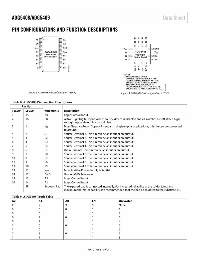
PIN CONFIGURATIONS AND FUNCTION DESCRIPTIONS
1
2
3
4
5
6
7
8
16
15
14
13
12
11
10
9
EN
VSS
S1
S4
S3
S2
A0
A2
GND
VDD
S7
D S8
S6
S5
A1
ADG5408TOP VIEW
(Not to Scale)
0920
6-00
2
Figure 2. ADG5408 Pin Configuration (TSSOP)
1VSS
NOTES1. THE EXPOSED PAD IS CONNECTED INTERNALLY. FOR INCREASED RELIABILITY OF THE SOLDER JOINTS AND MAXIMUM THERMAL CAPABILITY, IT IS RECOMMENDED THAT THE PAD BE SOLDERED TO THE SUBSTRATE, VSS.
2S13S24S3
11 VDD
12 GND
10 S5
9 S6
5S4
6D
7S8
8S7
15A
0
16EN
14A
1
13A
2
0920
6-00
3
TOP VIEW(Not to Scale)
ADG5408
Figure 3. ADG5408 Pin Configuration (LFCSP)
Table 8. ADG5408 Pin Function Descriptions Pin No.
TSSOP LFCSP Mnemonic Description 1 15 A0 Logic Control Input. 2 16 EN Active High Digital Input. When low, the device is disabled and all switches are off. When high,
Ax logic inputs determine on switches. 3 1 VSS Most Negative Power Supply Potential. In single-supply applications, this pin can be connected
to ground. 4 2 S1 Source Terminal 1. This pin can be an input or an output. 5 3 S2 Source Terminal 2. This pin can be an input or an output. 6 4 S3 Source Terminal 3. This pin can be an input or an output. 7 5 S4 Source Terminal 4. This pin can be an input or an output. 8 6 D Drain Terminal. This pin can be an input or an output. 9 7 S8 Source Terminal 8. This pin can be an input or an output. 10 8 S7 Source Terminal 7. This pin can be an input or an output. 11 9 S6 Source Terminal 6. This pin can be an input or an output. 12 10 S5 Source Terminal 5. This pin can be an input or an output. 13 11 VDD Most Positive Power Supply Potential. 14 12 GND Ground (0 V) Reference. 15 13 A2 Logic Control Input. 16 14 A1 Logic Control Input. EP Exposed Pad The exposed pad is connected internally. For increased reliability of the solder joints and
maximum thermal capability, it is recommended that the pad be soldered to the substrate, VSS.
Table 9. ADG5408 Truth Table A2 A1 A0 EN On Switch X X X 0 None 0 0 0 1 1 0 0 1 1 2 0 1 0 1 3 0 1 1 1 4 1 0 0 1 5 1 0 1 1 6 1 1 0 1 7 1 1 1 1 8

Data Sheet ADG5408/ADG5409
Rev. C | Page 11 of 24
1
2
3
4
5
6
7
8
16
15
14
13
12
11
10
9
EN
VSS
S1A
S4A
S3A
S2A
A0
GND
VDD
S1B
S4B
DA DB
S3B
S2B
A1
ADG5409TOP VIEW
(Not to Scale)
0920
6-00
4
Figure 4. ADG5409 Pin Configuration (TSSOP)
1VSS
2S1A3S2A
4S3A
11 S1B
12 VDD
10 S2B
9 S3B
5S4
A
6D
A
7D
B
8S4
B
15A
0
16EN
14A
1
13G
ND
NOTES1. THE EXPOSED PAD IS CONNECTED INTERNALLY. FOR INCREASED RELIABILITY OF THE SOLDER JOINTS AND MAXIMUM THERMAL CAPABILITY, IT IS RECOMMENDED THAT THE PAD BE SOLDERED TO THE SUBSTRATE, VSS.
0920
6-00
5
TOP VIEW(Not to Scale)
ADG5409
Figure 5. ADG5409 Pin Configuration (LFCSP)
Table 10. ADG5409 Pin Function Descriptions Pin No.
TSSOP LFCSP Mnemonic Description 1 15 A0 Logic Control Input. 2 16 EN Active High Digital Input. When low, the device is disabled and all switches are off. When high,
Ax logic inputs determine on switches. 3 1 VSS Most Negative Power Supply Potential. In single-supply applications, this pin can be connected
to ground. 4 2 S1A Source Terminal 1A. This pin can be an input or an output. 5 3 S2A Source Terminal 2A. This pin can be an input or an output. 6 4 S3A Source Terminal 3A. This pin can be an input or an output. 7 5 S4A Source Terminal 4A. This pin can be an input or an output. 8 6 DA Drain Terminal A. This pin can be an input or an output. 9 7 DB Drain Terminal B. This pin can be an input or an output. 10 8 S4B Source Terminal 4B. This pin can be an input or an output. 11 9 S3B Source Terminal 3B. This pin can be an input or an output. 12 10 S2B Source Terminal 2B. This pin can be an input or an output. 13 11 S1B Source Terminal 1B. This pin can be an input or an output. 14 12 VDD Most Positive Power Supply Potential. 15 13 GND Ground (0 V) Reference. 16 14 A1 Logic Control Input. EP Exposed
Pad The exposed pad is connected internally. For increased reliability of the solder joints and maximum thermal capability, it is recommended that the pad be soldered to the substrate, VSS.
Table 11. ADG5409 Truth Table A1 A0 EN On Switch Pair X X 0 None 0 0 1 1 0 1 1 2 1 0 1 3 1 1 1 4

ADG5408/ADG5409 Data Sheet
Rev. C | Page 12 of 24
TYPICAL PERFORMANCE CHARACTERISTICS
0
5
10
15
20
25
–18 –14 –10 –6 –2 2 6 10 14 18
ON
RES
ISTA
NC
E (Ω
)
VS, VD (V)
TA = 25°CVDD = +9VVSS = –9V
VDD = +10VVSS = –10V
VDD = +11VVSS = –11V
VDD = +13.5VVSS = –13.5V VDD = +15V
VSS = –15VVDD = +16.5VVSS = –16.5V
0920
6-02
8
Figure 6. RON as a Function of VS, VD (Dual Supply)
0
2
4
6
8
10
12
14
16
–25 –20 –15 –10 –5 0 5 10 15 20 25
ON
RES
ISTA
NC
E (Ω
)
VS, VD (V)
TA = 25°C
VDD = +22VVSS = –22V
VDD = +20VVSS = –20V
VDD = +18VVSS = –18V
0920
6-02
9
Figure 7. RON as a Function of VS, VD (Dual Supply)
0
–5
–10
–15
–20
–25
–30
–35
0 –2 –4 –6 –8 –10 –12 –14
ON
RES
ISTA
NC
E (Ω
)
VS, VD (V)
TA = 25°C
VDD = 9VVSS = 0V
VDD = 10VVSS = 0V VDD = 10.8V
VSS = 0V
VDD = 11VVSS = 0VVDD = 12V
VSS = 0VVDD = 13.2VVSS = 0V
0920
6-02
3
Figure 8. RON as a Function of VS, VD (Single Supply)
0
2
4
6
8
10
12
14
16
0 5 10 15 20 25 30 35 40 45
ON
RES
ISTA
NC
E (Ω
)
VS, VD (V)
TA = 25°C
VDD = 39.6VVSS = 0V
VDD = 36VVSS = 0V
VDD = 32.4VVSS = 0V
0920
6-02
7
Figure 9. RON as a Function of VS, VD (Single Supply)
0
5
10
15
20
25
–15 –10 –5 0 5 10 15
ON
RES
ISTA
NC
E (Ω
)
VS, VD (V)
VDD = +15VVSS = –15V
TA = +125°C
TA = +85°C
TA = +25°C
TA = –40°C
0920
6-03
0
Figure 10. RON as a Function of VS (VD) for Different Temperatures,
±15 V Dual Supply
0
5
10
15
20
25
–20 –15 –10 –5 0 5 10 15 20
ON
RES
ISTA
NC
E (Ω
)
TA = +125°C
TA = +85°C
TA = +25°C
TA = –40°C
VS, VD (V)
VDD = +20VVSS = –20V
0920
6-02
4
Figure 11. RON as a Function of VS (VD) for Different Temperatures,
±20 V Dual Supply

Data Sheet ADG5408/ADG5409
Rev. C | Page 13 of 24
0
5
10
15
20
25
30
35
40
0 2 4 6 8 10 12
VS, VD (V)
ON
RES
ISTA
NC
E (Ω
)
TA = +125°C
TA = +85°C
TA = +25°C
TA = –40°C
VDD = 12VVSS = 0V
0920
6-03
1
Figure 12. RON as a Function of VS (VD) for Different Temperatures,
12 V Single Supply
0
5
10
15
20
25
0 5 10 15 20 25 30 35 40
ON
RES
ISTA
NC
E (Ω
)
TA = +125°C
TA = +85°C
TA = +25°C
TA = –40°C
VS, VD (V)
VDD = 36VVSS = 0V
0920
6-03
2
Figure 13. RON as a Function of VD (VS) for Different Temperatures,
36 V Single Supply
0 25 50 75 100 125
LEA
KA
GE
CU
RR
ENT
(nA
)
TEMPERATURE (°C)
0.5
–1.0
0
–2.0
–0.5
–1.5
VDD = +15VVSS = –15VVBIAS = +10V/–10V
ID, IS (ON) + +
ID, IS (ON) – –
ID (OFF) + –
IS (OFF) + –
IS (OFF) – + ID (OFF) – +
0920
6-03
4
Figure 14. Leakage Currents vs. Temperature, ±15 V Dual Supply
0 25 50 75 100 125
LEA
KA
GE
CU
RR
ENT
(nA
)
TEMPERATURE (°C)
1
–1
0
–3
–2
VDD = +20VVSS = –20VVBIAS = +15V/–15V
ID, IS (ON) + +
ID, IS (ON) – –
ID (OFF) + –
IS (OFF) + –
IS (OFF) – +ID (OFF) – +
0920
6-03
5
Figure 15. Leakage Currents vs. Temperature, ±20 V Dual Supply
0 25 50 75 100 125
LEA
KA
GE
CU
RR
ENT
(nA
)
TEMPERATURE (°C)
0.5
–1.0
0
–2.0
–0.5
–1.5
VDD = 12VVSS = 0VVBIAS = 1V/10V
ID, IS (ON) + +
ID, IS (ON) – –
ID (OFF) + –
IS (OFF) + –
ID (OFF) – +
IS (OFF) – +
0920
6-03
3
Figure 16. Leakage Currents vs. Temperature, 12 V Single Supply
0 25 50 75 100 125
LEA
KA
GE
CU
RR
ENT
(nA
)
TEMPERATURE (°C)
1
–1
0
–3
–2
VDD = +36VVSS = 0VVBIAS = 1V/30V
ID, IS (ON) + +
ID, IS (ON) – –
ID (OFF) + –
IS (OFF) + –
IS (OFF) – +ID (OFF) – +
0920
6-03
6
Figure 17. Leakage Currents vs. Temperature, 36 V Single Supply

ADG5408/ADG5409 Data Sheet
Rev. C | Page 14 of 24
–100
–90
–80
–70
–60
–50
–40
–30
–20
–10
0
OFF
ISO
LATI
ON
(dB
)
FREQUENCY (Hz)
100k10k 1M 10M 100M 1G1k
TA = 25°CVDD = +15VVSS = –15V
0920
6-02
1
Figure 18. Off Isolation vs. Frequency, ±15 V Dual Supply
–100
–90
–80
–70
–60
–50
–40
–30
–20
–10
0
CR
OSS
TALK
(dB
)
FREQUENCY (Hz)
10k 100k 1M 10M 100M 1G
TA = 25°CVDD = +15VVSS = –15V
0920
6-02
6
Figure 19. Crosstalk vs. Frequency, ±15 V Dual Supply
0
50
100
150
200
250
300
20 10 0 10 20 30 40
CH
AR
GE
INJE
CTI
ON
(pC
)
TA = 25°C VDD = +20VVSS = –20V
VDD = +15VVSS = –15V
VDD = +36VVSS = 0V
VDD = +12VVSS = 0V
VS (V) 0920
6-01
9
Figure 20. Charge Injection vs. Source Voltage
–100
–90
–80
–70
–60
–50
–40
–30
–20
–10
0
AC
PSR
R (d
B)
FREQUENCY (Hz)
1k 1M 10M10k 100k
TA = 25°CVDD = +15VVSS = –15V
NO DECOUPLINGCAPACITORS
DECOUPLINGCAPACITORS
0920
6-02
2
Figure 21. ACPSRR vs. Frequency, ±15 V Dual Supply
0
0.02
0.04
0.06
0.08
0.10
0.12
0 5 10 15 20
THD
+ N
(%)
FREQUENCY (kHz)
VDD = 12V, VSS = 0V, VS = 6V p-p
VDD = 36V, VSS = 0V, VS = 18V p-p
VDD = 15V, VSS = 15V, VS = 15V p-p
VDD = 20V, VSS = 20V, VS = 20V p-p
LOAD = 1kΩTA = 25°C
0920
6-02
5
Figure 22. THD + N vs. Frequency
–5.0
–4.5
–4.0
–3.5
–3.0
–2.5
–2.0
–1.5
–1.0
–0.5
0
INSE
RTI
ON
LO
SS (d
B)
FREQUENCY (Hz)
10k 100k 1M 10M 100M1k 1G
ADG5408
ADG5409
TA = 25°CVDD = +15VVSS = –15V
0920
6-02
0
Figure 23. Bandwidth

Data Sheet ADG5408/ADG5409
Rev. C | Page 15 of 24
0
50
100
150
200
250
300
350
400
–40 –20 0 20 40 60 80 100 120
TIM
E (n
s)
VDD = +12V, VSS = 0V
VDD = +15V, VSS = –15V
VDD = +36V, VSS = 0V
VDD = +20V, VSS = –20V
TEMPERATURE (°C) 0920
6-01
8
Figure 24. tTRANSITION Times vs. Temperature

ADG5408/ADG5409 Data Sheet
Rev. C | Page 16 of 24
TEST CIRCUITS
0920
6-00
8
S2
VD VD
S8
S1 DID (ON)
NC
NC = NO CONNECT
A
Figure 25. On Leakage
0920
6-00
6
IDS
S D
VS
V
RON = V/IDS
Figure 26. On Resistance
CHANNEL-TO-CHANNEL CROSSTALK = 20 logVOUT
GND
S1
D
S2
VOUT
NETWORKANALYZER
RL50Ω
RL50Ω
VS
VS
VDD VSS
0.1µF
VDD
0.1µF
VSS
0920
6-01
4
Figure 27. Channel-to-Channel Crosstalk
VOUT
50Ω
NETWORKANALYZER
RL50Ω
Sx
D
VS
VDD VSS
0.1µF
VDD
0.1µF
VSS
GND
50Ω
OFF ISOLATION = 20 logVOUT
VS 0920
6-01
3
Figure 28. Off Isolation
0920
6-00
7
S1 D
VS VD
IS (OFF)
S8
ID (OFF)
AA
A
Figure 29. Off Leakage
VOUT
RS
AUDIO PRECISION
RL10kΩ
IN
VIN
Sx
D
VSV p-p
VDD VSS
0.1µF
VDD
0.1µF
VSS
GND
0920
6-01
5
Figure 30. THD + Noise Figure
VOUT
50Ω
NETWORKANALYZER
RL50Ω
Sx
D
INSERTION LOSS = 20 logVOUT WITH SWITCH
VOUT WITHOUT SWITCH
VS
VDD VSS
0.1µF
VDD
0.1µF
VSS
GND
0920
6-01
7Figure 31. Bandwidth

Data Sheet ADG5408/ADG5409
Rev. C | Page 17 of 24
3V
0V
OUTPUT
tr < 20nstf < 20ns
ADDRESSDRIVE (VIN)
tTRANSITION tTRANSITION
50% 50%
90%
90%
OUTPUTADG5408*
A0
A1
A2
50Ω
300ΩGND
S1
S2 TO S7
S8
D
35pF
VIN
2.4V EN
VDD VSS
VDD VSS
VS1
VS8
*SIMILAR CONNECTION FOR ADG5409. 0920
6-00
9
Figure 32. Address to Output Switching Times, tTRANSITION
OUTPUTADG5408*
A0
A1
A2
50Ω
300ΩGND
S1
S2 TO S7
S8
D
35pF
VIN
2.4V EN
VDD VSS
VDD VSS
VS
*SIMILAR CONNECTION FOR ADG5409.
3V
0V
OUTPUT80% 80%
ADDRESSDRIVE (VIN)
tD
0920
6-01
0
Figure 33. Break-Before-Make Delay, tD
OUTPUTADG5408*
A0
A1
A2
50Ω 300ΩGND
S1
S2 TO S8
D
35pFVIN
EN
VDD VSS
VDD VSS
VS
*SIMILAR CONNECTION FOR ADG5409.
3V
0V
OUTPUT
50% 50%
tOFF (EN)tON (EN)
0.9VO 0.9VO
ENABLEDRIVE (VIN)
0920
6-01
1
Figure 34. Enable Delay, tON (EN), tOFF (EN)
3V
VIN
VOUT
QINJ = CL × ∆VOUT
∆VOUTDSx
EN
GNDCL1nF
VOUT
VIN
RS
VS
VDD VSS
VDD VSS
A0
A1
A2
ADG5408*
*SIMILAR CONNECTION FOR ADG5409. 0920
6-01
2
Figure 35. Charge Injection

ADG5408/ADG5409 Data Sheet
Rev. C | Page 18 of 24
TERMINOLOGY IDD IDD represents the positive supply current.
ISS ISS represents the negative supply current.
VD, VS VD and VS represent the analog voltage on Terminal D and Terminal S, respectively.
RON RON is the ohmic resistance between Terminal D and Terminal S.
∆RON ∆RON represents the difference between the RON of any two channels.
RFLAT (ON) The difference between the maximum and minimum value of on resistance as measured over the specified analog signal range is represented by RFLAT (ON).
IS (Off) IS (Off) is the source leakage current with the switch off.
ID (Off) ID (Off) is the drain leakage current with the switch off.
ID (On), IS (On) ID (On) and IS (On) represent the channel leakage currents with the switch on.
VINL VINL is the maximum input voltage for Logic 0.
VINH VINH is the minimum input voltage for Logic 1.
IINL, IINH IINL and IINH represent the low and high input currents of the digital inputs.
CD (Off) CD (Off) represents the off switch drain capacitance, which is measured with reference to ground.
CS (Off) CS (Off) represents the off switch source capacitance, which is measured with reference to ground.
CD (On), CS (On) CD (On) and CS (On) represent on switch capacitances, which are measured with reference to ground.
CIN CIN represents digital input capacitance.
tON (EN) tON (EN) represents the delay time between the 50% and 90% points of the digital input and switch on condition.
tOFF (EN) tOFF (EN) represents the delay time between the 50% and 90% points of the digital input and switch off condition.
tTRANSITION Delay time between the 50% and 90% points of the digital inputs and the switch on condition when switching from one address state to another.
tD
tD represents the off time measured between the 80% point of both switches when switching from one address state to another.
Off Isolation Off isolation is a measure of unwanted signal coupling through an off channel.
Charge Injection Charge injection is a measure of the glitch impulse transferred from the digital input to the analog output during switching.
Crosstalk Crosstalk is a measure of unwanted signal that is coupled through from one channel to another as a result of parasitic capacitance.
Bandwidth Bandwidth is the frequency at which the output is attenuated by 3 dB.
On Response On response is the frequency response of the on switch.
Total Harmonic Distortion + Noise (THD + N) The ratio of the harmonic amplitude plus noise of the signal to the fundamental is represented by THD + N.
AC Power Supply Rejection Ratio (ACPSRR) ACPSRR is a measure of the ability of a part to avoid coupling noise and spurious signals that appear on the supply voltage pin to the output of the switch. The dc voltage on the device is modulated by a sine wave of 0.62 V p-p. The ratio of the amplitude of signal on the output to the amplitude of the modulation is the ACPSRR.

Data Sheet ADG5408/ADG5409
Rev. C | Page 19 of 24
TRENCH ISOLATION In the ADG5408/ADG5409, an insulating oxide layer (trench) is placed between the NMOS and the PMOS transistors of each CMOS switch. Parasitic junctions, which occur between the transistors in junction isolated switches, are eliminated, and the result is a completely latch-up proof switch.
In junction isolation, the N and P wells of the PMOS and NMOS transistors form a diode that is reverse-biased under normal operation. However, during overvoltage conditions, this diode can become forward-biased. A silicon controlled rectifier (SCR) type circuit is formed by the two transistors causing a significant amplification of the current that, in turn, leads to latch-up. With trench isolation, this diode is removed, and the result is a latch-up proof switch.
0920
6-01
6
NMOS PMOS
P-WELL N-WELL
BURIED OXIDE LAYER
HANDLE WAFER
TRENCH
Figure 36. Trench Isolation

ADG5408/ADG5409 Data Sheet
Rev. C | Page 20 of 24
APPLICATIONS INFORMATION The ADG54xx family switches and multiplexers provide a robust solution for instrumentation, industrial, aerospace, and other harsh environments that are prone to latch-up, which is an undesirable high current state that can lead to device failure and persist until the power supply is turned off. The ADG5408/ ADG5409 high voltage switches allow single-supply operation
from 9 V to 40 V and dual-supply operation from ±9 V to ±22 V. The ADG5408/ADG5409 (as well as select devices within the same family) achieve an 8 kV human body model ESD rating that provides a robust solution eliminating the need for separate protect circuitry designs in some applications.

Data Sheet ADG5408/ADG5409
Rev. C | Page 21 of 24
OUTLINE DIMENSIONS
16 9
81
PIN 1
SEATINGPLANE
8°0°
4.504.404.30
6.40BSC
5.105.004.90
0.65BSC
0.150.05
1.20MAX
0.200.09 0.75
0.600.45
0.300.19
COPLANARITY0.10
COMPLIANT TO JEDEC STANDARDS MO-153-AB Figure 37. 16-Lead Thin Shrink Small Outline Package [TSSOP]
(RU-16) Dimensions shown in millimeters
2.702.60 SQ2.50
COMPLIANT TO JEDEC STANDARDS MO-220-WGGC.
1
0.65BSC
BOTTOM VIEWTOP VIEW
16
589
1213
4
EXPOSEDPAD
PIN 1INDICATOR
4.104.00 SQ3.90
0.450.400.35
SEATINGPLANE
0.800.750.70 0.05 MAX
0.02 NOM
0.20 REF
0.20 MIN
COPLANARITY0.08
PIN 1INDICATOR
0.350.300.25
FOR PROPER CONNECTION OFTHE EXPOSED PAD, REFER TOTHE PIN CONFIGURATION ANDFUNCTION DESCRIPTIONSSECTION OF THIS DATA SHEET.
08-1
6-20
10-C
Figure 38. 16-Lead Lead Frame Chip Scale Package [LFCSP_WQ]
4 mm × 4 mm Body, Very Very Thin Quad (CP-16-17)
Dimensions shown in millimeters

ADG5408/ADG5409 Data Sheet
Rev. C | Page 22 of 24
ORDERING GUIDE Model1 Temperature Range Package Description Package Option ADG5408BRUZ −40°C to +125°C 16-Lead Thin Shrink Small Outline Package [TSSOP] RU-16 ADG5408BRUZ-REEL7 −40°C to +125°C 16-Lead Thin Shrink Small Outline Package [TSSOP] RU-16 ADG5408BCPZ-REEL7 −40°C to +125°C 16-Lead Lead Frame Chip Scale Package [LFCSP_WQ] CP-16-17 ADG5409BRUZ −40°C to +125°C 16-Lead Thin Shrink Small Outline Package [TSSOP] RU-16 ADG5409BRUZ-REEL7 −40°C to +125°C 16-Lead Thin Shrink Small Outline Package [TSSOP] RU-16 ADG5409BCPZ-REEL7 −40°C to +125°C 16-Lead Lead Frame Chip Scale Package [LFCSP_WQ] CP-16-17 1 Z = RoHS Compliant Part.

Data Sheet ADG5408/ADG5409
Rev. C | Page 23 of 24
NOTES
ADG5408/ADG5409 Data Sheet
Rev. C | Page 24 of 24
NOTES
©2010–2013 Analog Devices, Inc. All rights reserved. Trademarks and registered trademarks are the property of their respective owners. D09206-0-3/13(C)