LOGIC CIRCUITS Ho Kyung Kim, Ph.D. [email protected] School of Mechanical Engineering Pusan National University Basic Experiment and Design of Electronics

Welcome message from author
This document is posted to help you gain knowledge. Please leave a comment to let me know what you think about it! Share it to your friends and learn new things together.
Transcript
LOGIC CIRCUITS
Ho Kyung Kim, Ph.D.
School of Mechanical Engineering
Pusan National University
Basic Experiment and Design of Electronics
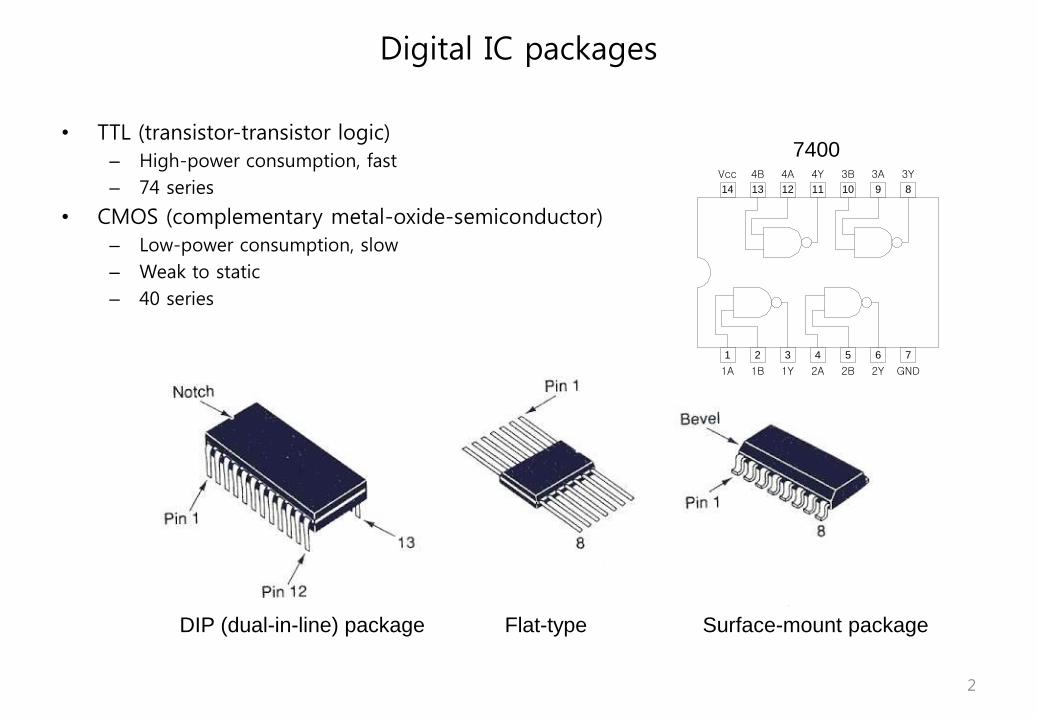
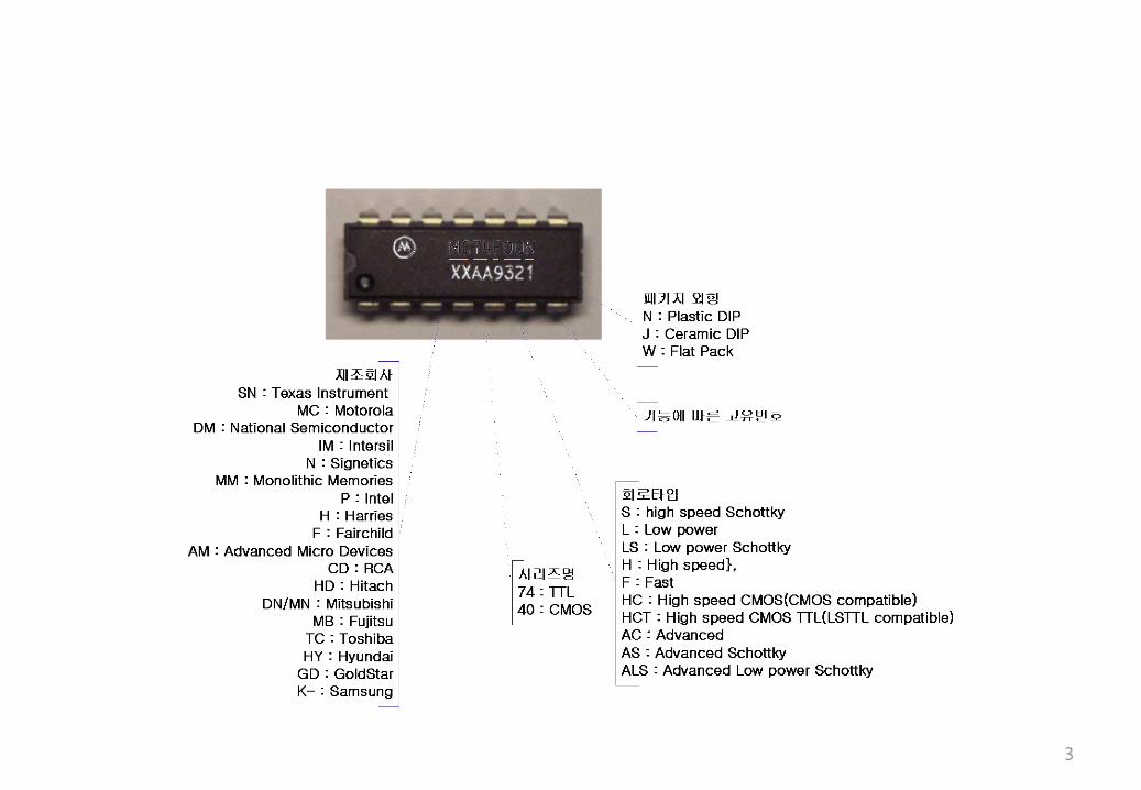
Digital IC packages
• TTL (transistor-transistor logic)
– High-power consumption, fast
– 74 series
• CMOS (complementary metal-oxide-semiconductor)
– Low-power consumption, slow
– Weak to static
– 40 series
2
1 2 3 4 5 6 7
814 13 12 11 10 9
1Y 2A1A 1B
Vcc 4Y 3B4B
2B GND
3A4A
2Y
3Y
DIP (dual-in-line) package Flat-type Surface-mount package
7400
3
Outline
• Combinational logic circuits
– Output depends on only the present inputs; not on the past inputs
– Multiplex
– ROM
– Decoder
– RAM
– PLD
• Sequential logic circuits
– Output depends on both the present and past inputs; hence having “memory” function
– Flip-flops
– Counters
4
• Multiplex
• ROM
• Decoder
• RAM
• PLD
Combinational logic circuits (modules)
5
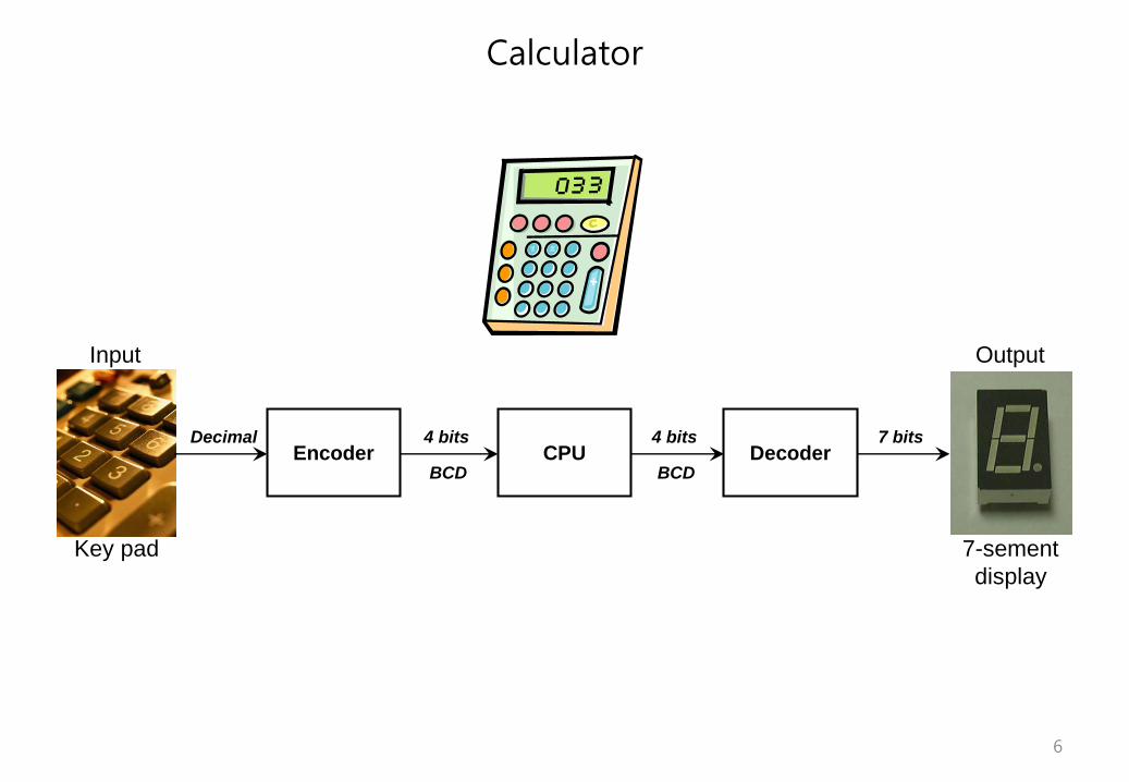
Calculator
Encoder CPU Decoder
Input
Key pad
Decimal 4 bits
BCD
4 bits
BCD
7 bits
Output
7-sement
display
6
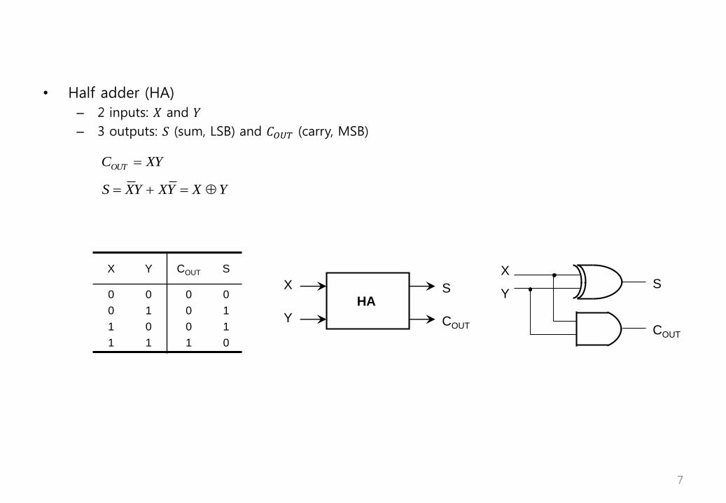
• Half adder (HA)
– 2 inputs: 𝑋 and 𝑌
– 3 outputs: 𝑆 (sum, LSB) and 𝐶𝑂𝑈𝑇 (carry, MSB)
X Y COUT S
0
0
1
1
0
1
0
1
0
0
0
1
0
1
1
0
HA
X
Y
S
COUT
X
YS
COUT
XYCOUT
YXYXYXS
7
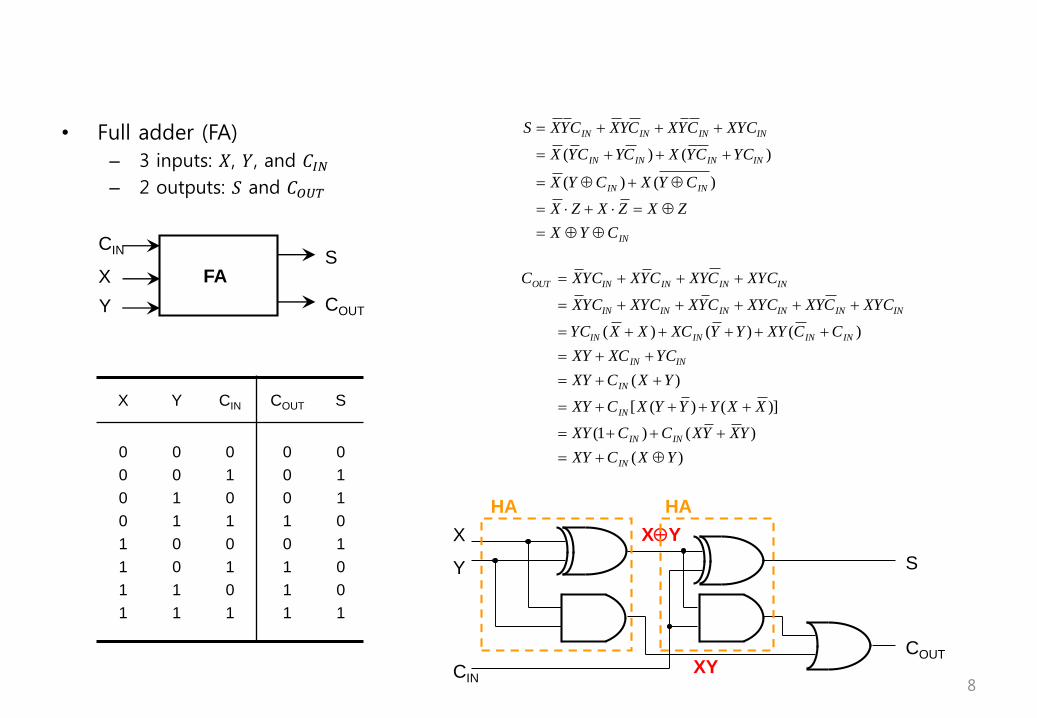
• Full adder (FA)
– 3 inputs: 𝑋, 𝑌, and 𝐶𝐼𝑁
– 2 outputs: 𝑆 and 𝐶𝑂𝑈𝑇
X Y CIN COUT S
0
0
0
0
1
1
1
1
0
0
1
1
0
0
1
1
0
1
0
1
0
1
0
1
0
0
0
1
0
1
1
1
0
1
1
0
1
0
0
1
IN
ININ
ININININ
ININININ
CYX
ZXZXZX
CYXCYX
YCCYXCYCYX
XYCCYXCYXCYXS
)()(
)()(
)(
)()1(
)]()([
)(
)()()(
YXCXY
YXYXCCXY
XXYYYXCXY
YXCXY
YCXCXY
CCXYYYXCXXYC
XYCCXYXYCCYXXYCYCX
XYCCXYCYXYCXC
IN
ININ
IN
IN
ININ
ININININ
ININININININ
ININININOUT
FAX
Y
S
COUT
CIN
X
Y
COUT
S
CINXY
XY
HA HA
8
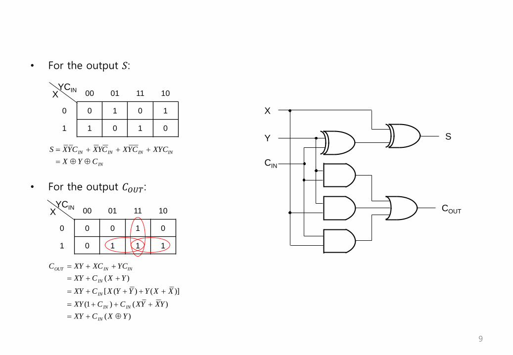
• For the output 𝑆:
• For the output 𝐶𝑂𝑈𝑇 :
00 01 11 10
0 0 1 0 1
1 1 0 1 0
YCINX
IN
ININININ
CYX
XYCCYXCYXCYXS
00 01 11 10
0 0 0 1 0
1 0 1 1 1
YCINX
)(
)()1(
)]()([
)(
YXCXY
YXYXCCXY
XXYYYXCXY
YXCXY
YCXCXYC
IN
ININ
IN
IN
ININOUT
Y S
COUT
X
CIN
9
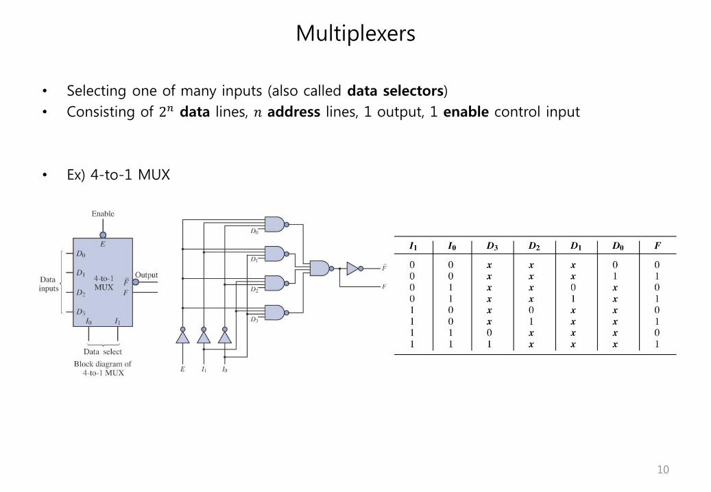
• Selecting one of many inputs (also called data selectors)
• Consisting of 2𝑛 data lines, 𝑛 address lines, 1 output, 1 enable control input
• Ex) 4-to-1 MUX
Multiplexers
10
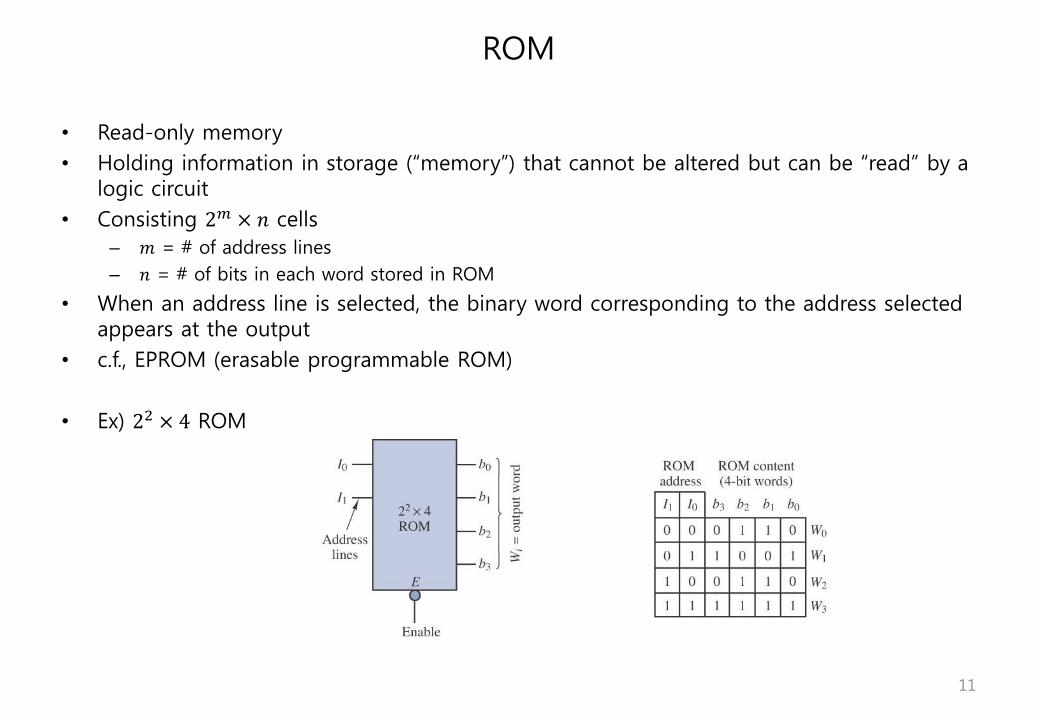
• Read-only memory
• Holding information in storage (“memory”) that cannot be altered but can be “read” by a logic circuit
• Consisting 2𝑚 × 𝑛 cells
– 𝑚 = # of address lines
– 𝑛 = # of bits in each word stored in ROM
• When an address line is selected, the binary word corresponding to the address selected appears at the output
• c.f., EPROM (erasable programmable ROM)
• Ex) 22 × 4 ROM
ROM
11
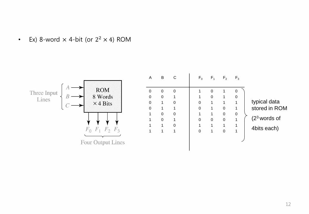
• Ex) 8-word × 4-bit (or 22 × 4) ROM
A B C F0 F1 F2 F3
0
0
0
0
1
1
1
1
0
0
1
1
0
0
1
1
0
1
0
1
0
1
0
1
1
1
0
0
1
0
1
0
0
0
1
1
1
0
1
1
1
1
1
0
0
0
1
0
0
0
1
1
0
1
1
1
typical data
stored in ROM
(23 words of
4bits each)
12
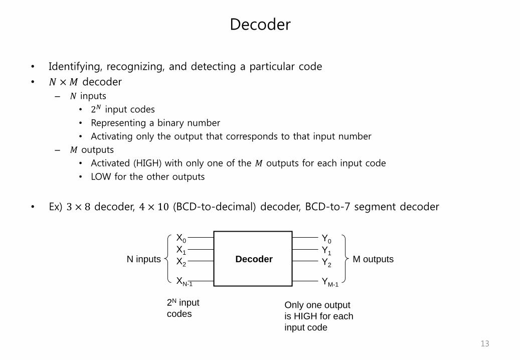
• Identifying, recognizing, and detecting a particular code
• 𝑁 × 𝑀 decoder
– 𝑁 inputs
• 2𝑁 input codes
• Representing a binary number
• Activating only the output that corresponds to that input number
– 𝑀 outputs
• Activated (HIGH) with only one of the 𝑀 outputs for each input code
• LOW for the other outputs
• Ex) 3 × 8 decoder, 4 × 10 (BCD-to-decimal) decoder, BCD-to-7 segment decoder
Decoder
Decoder
X0
X1
X2
XN-1
Y0
Y1
Y2
YM-1
2N input
codesOnly one output
is HIGH for each
input code
N inputs M outputs
13
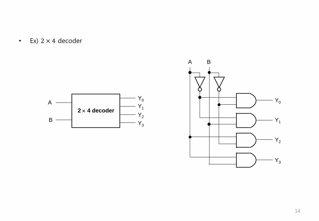
• Ex) 2 × 4 decoder
2 4 decoder
A
B
Y0
Y1
Y2
Y3
Y0
Y1
Y2
Y3
A B
14
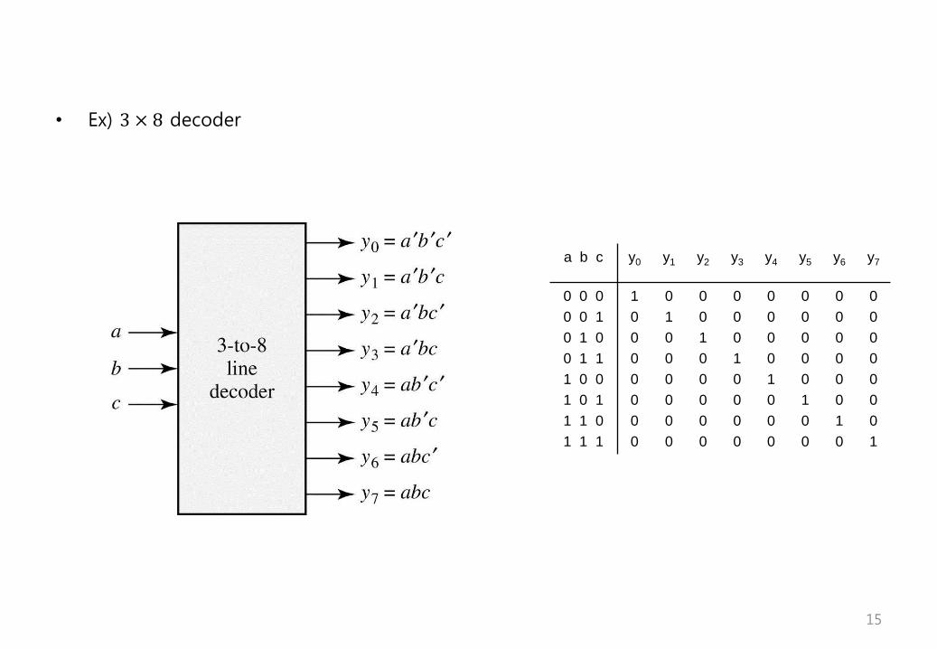
• Ex) 3 × 8 decoder
a b c y0 y1 y2 y3 y4 y5 y6 y7
0 0 0
0 0 1
0 1 0
0 1 1
1 0 0
1 0 1
1 1 0
1 1 1
1
0
0
0
0
0
0
0
0
1
0
0
0
0
0
0
0
0
1
0
0
0
0
0
0
0
0
1
0
0
0
0
0
0
0
0
1
0
0
0
0
0
0
0
0
1
0
0
0
0
0
0
0
0
1
0
0
0
0
0
0
0
0
1
15
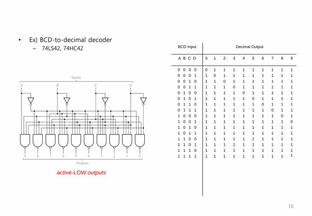
• Ex) BCD-to-decimal decoder
– 74LS42, 74HC42 BCD Input Decimal Output
A B C D 0 1 2 3 4 5 6 7 8 9
0 0 0 0
0 0 0 1
0 0 1 0
0 0 1 1
0 1 0 0
0 1 0 1
0 1 1 0
0 1 1 1
1 0 0 0
1 0 0 1
1 0 1 0
1 0 1 1
1 1 0 0
1 1 0 1
1 1 1 0
1 1 1 1
0
1
1
1
1
1
1
1
1
1
1
1
1
1
1
1
1
0
1
1
1
1
1
1
1
1
1
1
1
1
1
1
1
1
0
1
1
1
1
1
1
1
1
1
1
1
1
1
1
1
1
0
1
1
1
1
1
1
1
1
1
1
1
1
1
1
1
1
0
1
1
1
1
1
1
1
1
1
1
1
1
1
1
1
1
0
1
1
1
1
1
1
1
1
1
1
1
1
1
1
1
1
0
1
1
1
1
1
1
1
1
1
1
1
1
1
1
1
1
0
1
1
1
1
1
1
1
1
1
1
1
1
1
1
1
1
0
1
1
1
1
1
1
1
1
1
1
1
1
1
1
1
1
0
1
1
1
1
1
1
active-LOW outputs
16
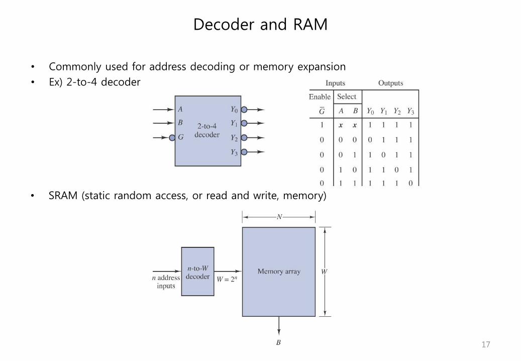
• Commonly used for address decoding or memory expansion
• Ex) 2-to-4 decoder
Decoder and RAM
• SRAM (static random access, or read and write, memory)
17
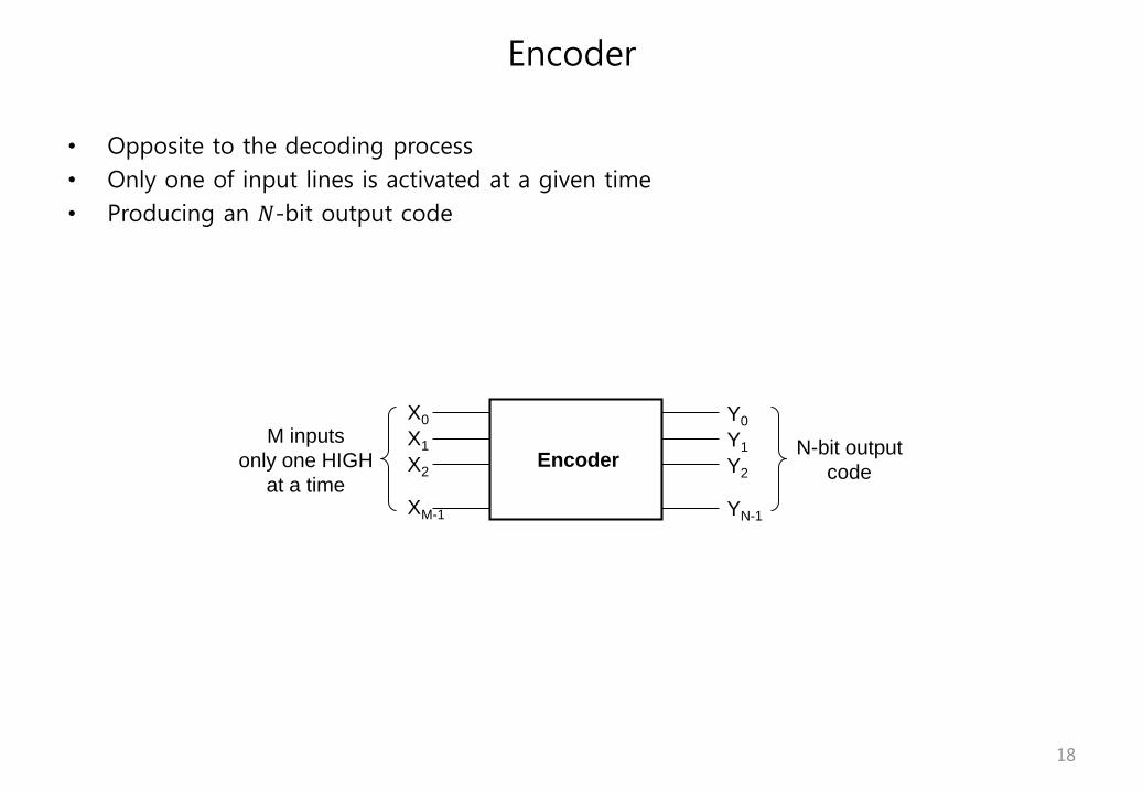
• Opposite to the decoding process
• Only one of input lines is activated at a given time
• Producing an 𝑁-bit output code
Encoder
Encoder
X0
X1
X2
XM-1
Y0
Y1
Y2
YN-1
M inputs
only one HIGH
at a time
N-bit output
code
18
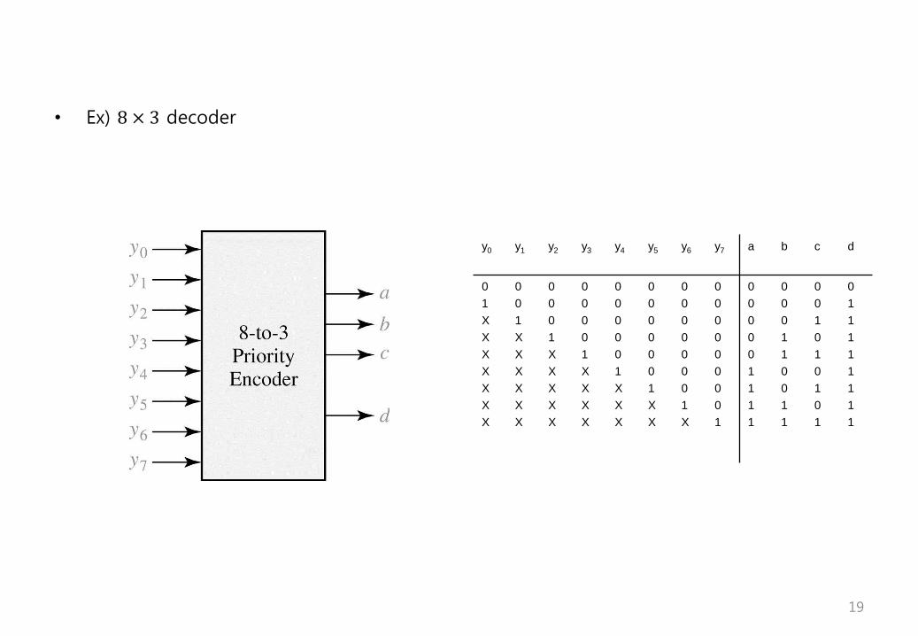
• Ex) 8 × 3 decoder
y0 y1 y2 y3 y4 y5 y6 y7 a b c d
0
1
X
X
X
X
X
X
X
0
0
1
X
X
X
X
X
X
0
0
0
1
X
X
X
X
X
0
0
0
0
1
X
X
X
X
0
0
0
0
0
1
X
X
X
0
0
0
0
0
0
1
X
X
0
0
0
0
0
0
0
1
X
0
0
0
0
0
0
0
0
1
0
0
0
0
0
1
1
1
1
0
0
0
1
1
0
0
1
1
0
0
1
0
1
0
1
0
1
0
1
1
1
1
1
1
1
1
19
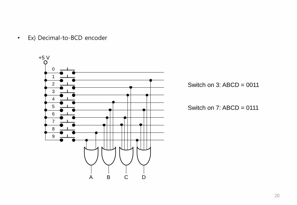
• Ex) Decimal-to-BCD encoder
A B C D
+5 V
0
1
2
3
4
5
6
7
8
9
Switch on 3: ABCD = 0011
Switch on 7: ABCD = 0111
20
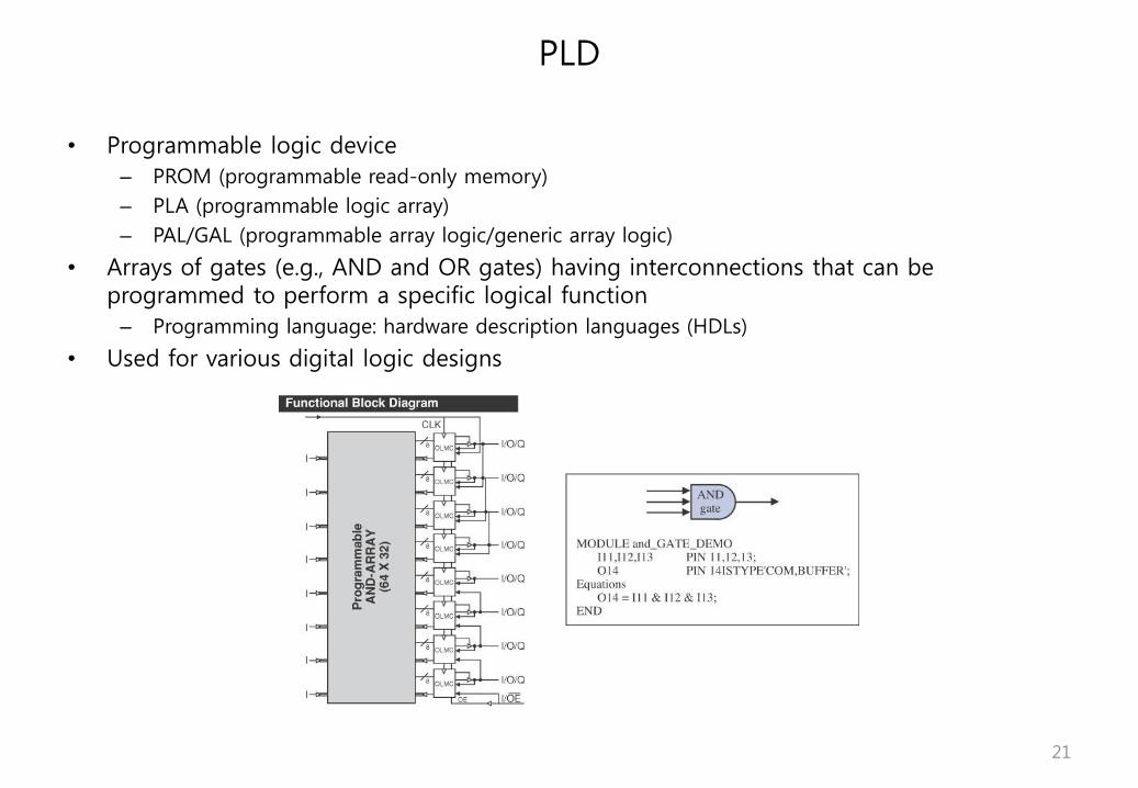
• Programmable logic device
– PROM (programmable read-only memory)
– PLA (programmable logic array)
– PAL/GAL (programmable array logic/generic array logic)
• Arrays of gates (e.g., AND and OR gates) having interconnections that can be programmed to perform a specific logical function
– Programming language: hardware description languages (HDLs)
• Used for various digital logic designs
PLD
21
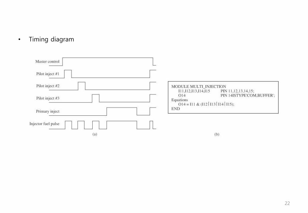
• Timing diagram
22
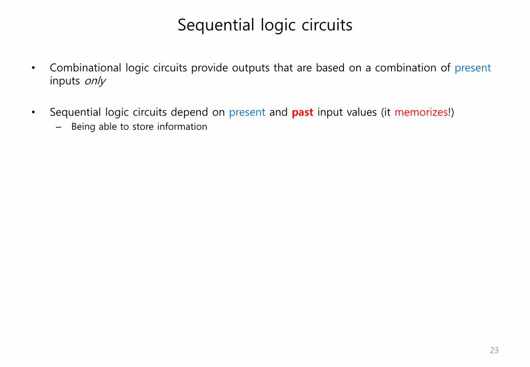
• Combinational logic circuits provide outputs that are based on a combination of present inputs only
• Sequential logic circuits depend on present and past input values (it memorizes!)
– Being able to store information
Sequential logic circuits
23
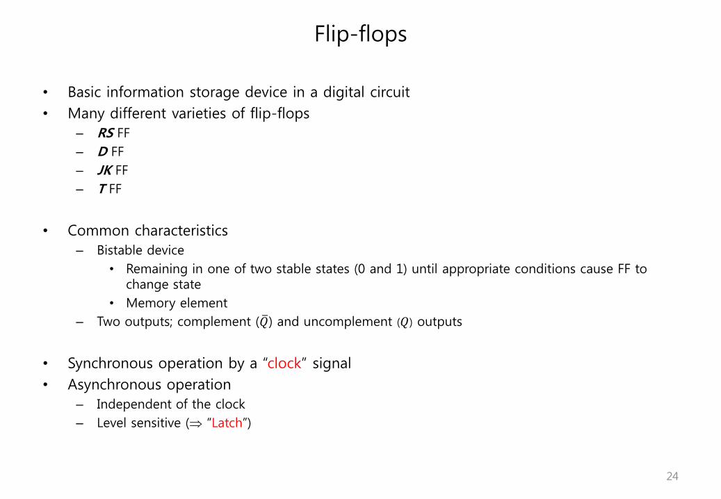
• Basic information storage device in a digital circuit
• Many different varieties of flip-flops
– RS FF
– D FF
– JK FF
– T FF
• Common characteristics
– Bistable device
• Remaining in one of two stable states (0 and 1) until appropriate conditions cause FF to change state
• Memory element
– Two outputs; complement ( 𝑄) and uncomplement (𝑄) outputs
• Synchronous operation by a “clock” signal
• Asynchronous operation
– Independent of the clock
– Level sensitive ( “Latch”)
Flip-flops
24
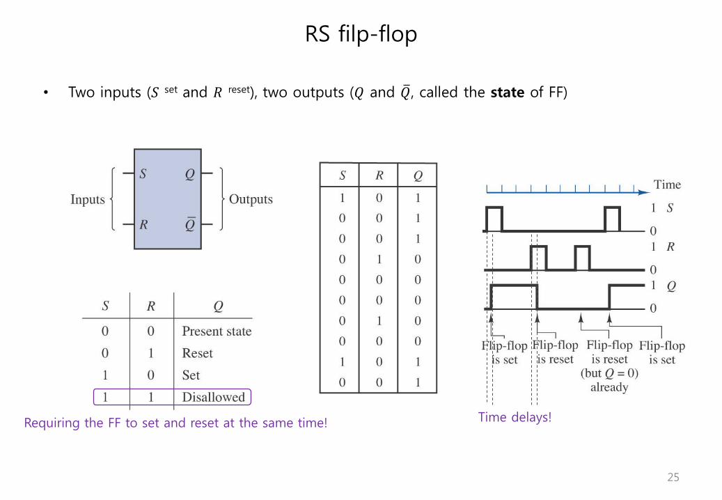
• Two inputs (𝑆 set and 𝑅 reset), two outputs (𝑄 and 𝑄, called the state of FF)
RS filp-flop
Requiring the FF to set and reset at the same time! Time delays!
25
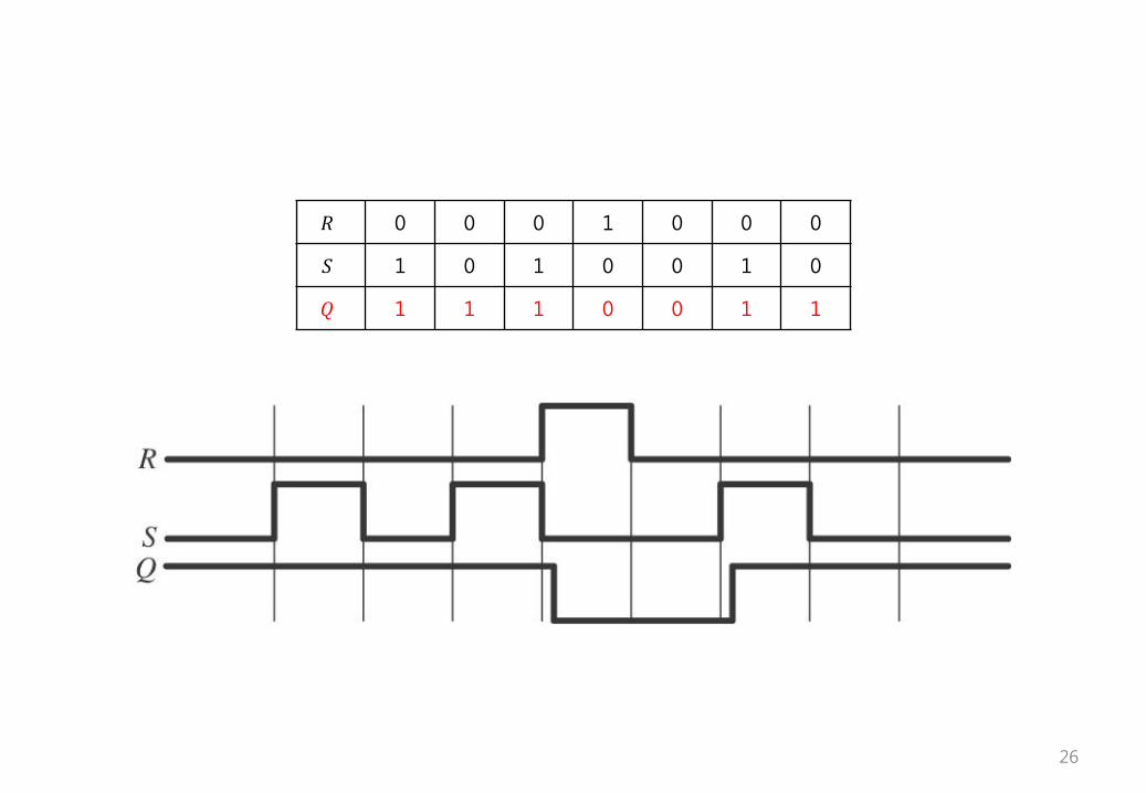
𝑅 0 0 0 1 0 0 0
𝑆 1 0 1 0 0 1 0
𝑄 1 1 1 0 0 1 1
26
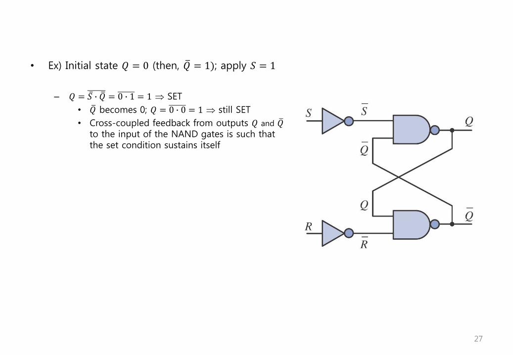
• Ex) Initial state 𝑄 = 0 (then, 𝑄 = 1); apply 𝑆 = 1
– 𝑄 = 𝑆 ∙ 𝑄 = 0 ∙ 1 = 1 SET
• 𝑄 becomes 0; 𝑄 = 0 ∙ 0 = 1 still SET
• Cross-coupled feedback from outputs 𝑄 and 𝑄to the input of the NAND gates is such that the set condition sustains itself
27
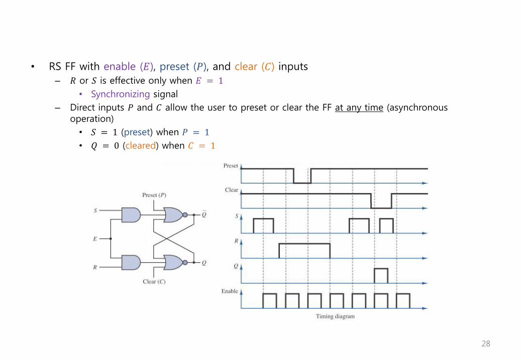
• RS FF with enable (𝐸), preset (𝑃), and clear (𝐶) inputs
– 𝑅 or 𝑆 is effective only when 𝐸 = 1
• Synchronizing signal
– Direct inputs 𝑃 and 𝐶 allow the user to preset or clear the FF at any time (asynchronous operation)
• 𝑆 = 1 (preset) when 𝑃 = 1
• 𝑄 = 0 (cleared) when 𝐶 = 1
28
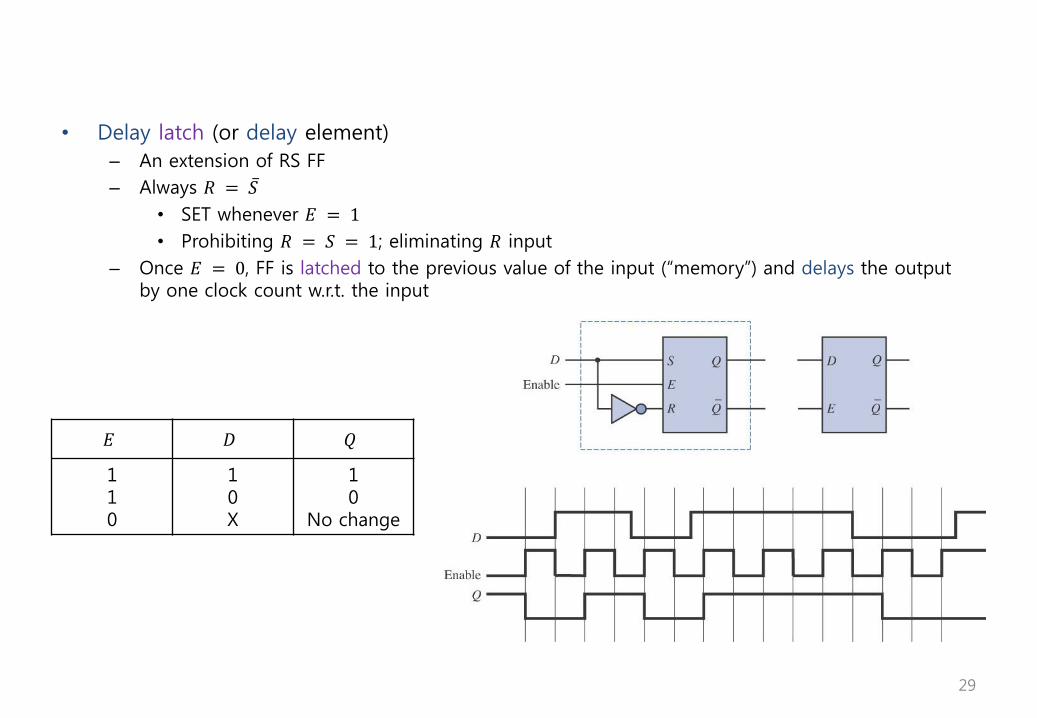
• Delay latch (or delay element)
– An extension of RS FF
– Always 𝑅 = 𝑆
• SET whenever 𝐸 = 1
• Prohibiting 𝑅 = 𝑆 = 1; eliminating 𝑅 input
– Once 𝐸 = 0, FF is latched to the previous value of the input (“memory”) and delays the output by one clock count w.r.t. the input
𝐸 𝐷 𝑄
110
10X
10
No change
29
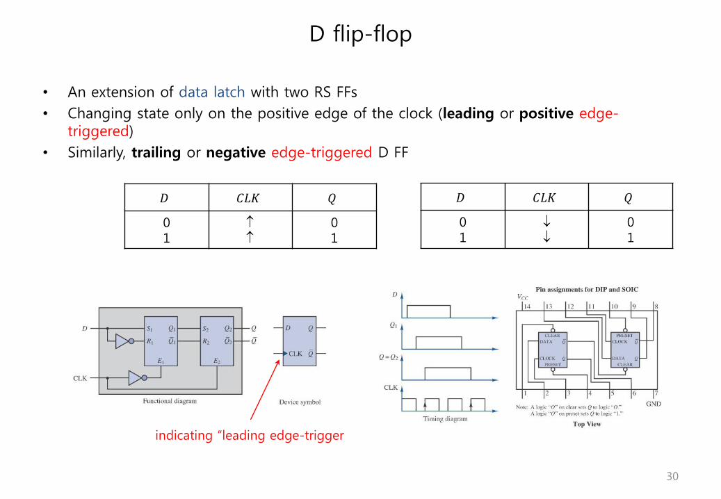
• An extension of data latch with two RS FFs
• Changing state only on the positive edge of the clock (leading or positive edge-triggered)
• Similarly, trailing or negative edge-triggered D FF
D flip-flop
𝐷 𝐶𝐿𝐾 𝑄
01
01
indicating “leading edge-trigger
𝐷 𝐶𝐿𝐾 𝑄
01
01
30
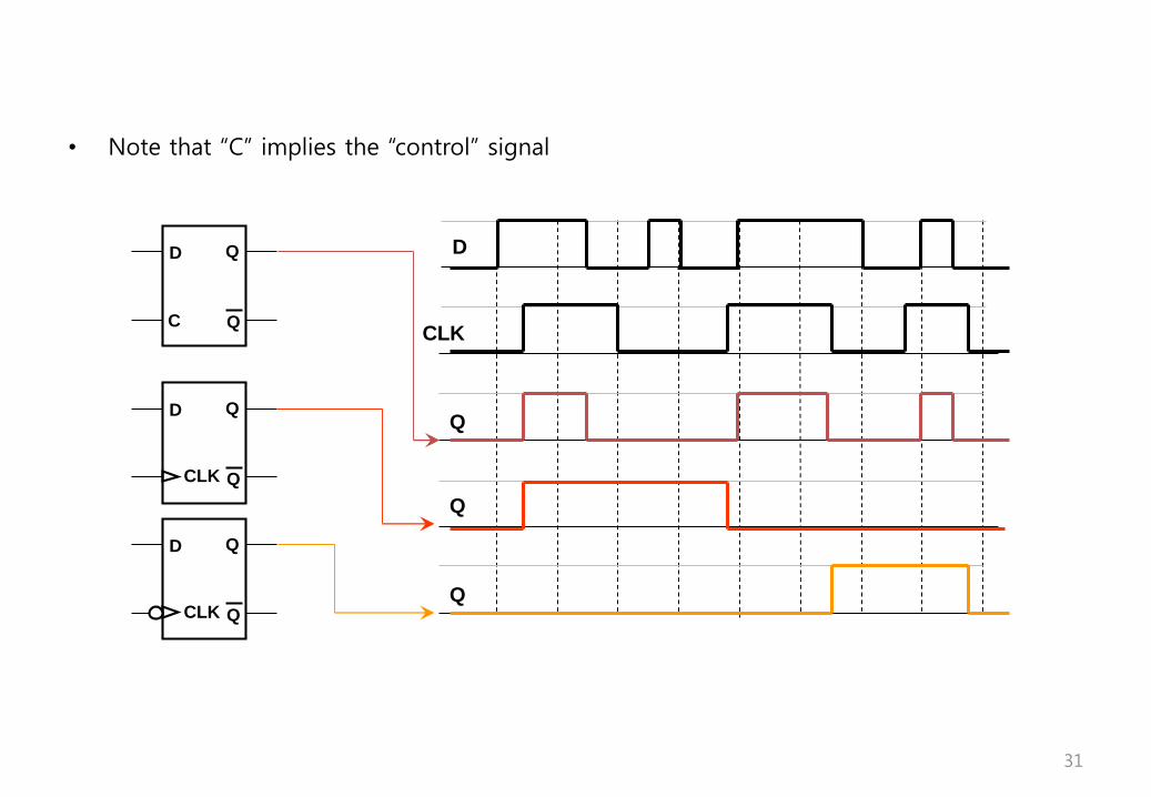
• Note that “C” implies the “control” signal
31
Q
Q
Q
CLK
DD
C
Q
Q
D Q
QCLK
D Q
QCLK
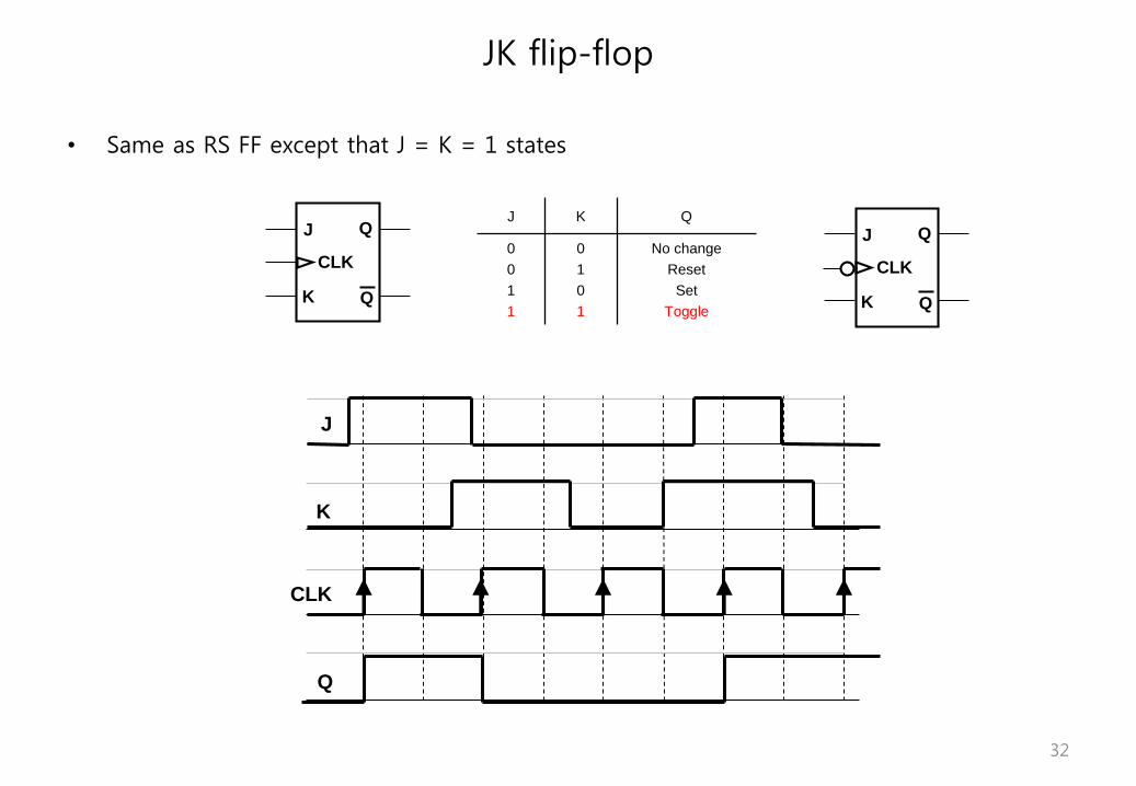
• Same as RS FF except that J = K = 1 states
JK flip-flop
32
J K Q
0
0
1
1
0
1
0
1
No change
Reset
Set
Toggle
J
K
Q
Q
CLK
J
K
Q
Q
CLK
K
CLK
Q
J
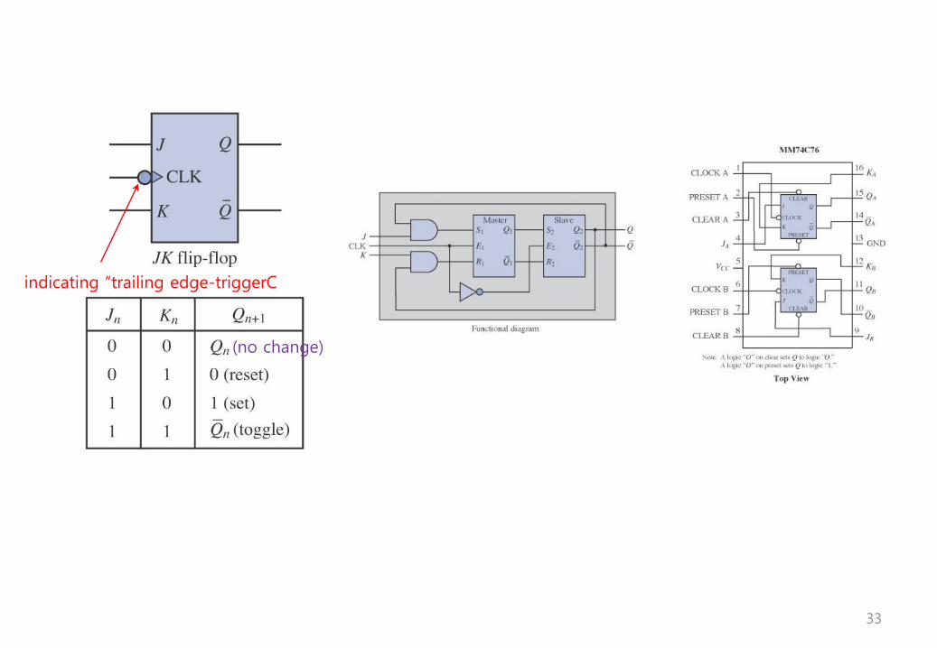
indicating “trailing edge-triggerC
(no change)
33
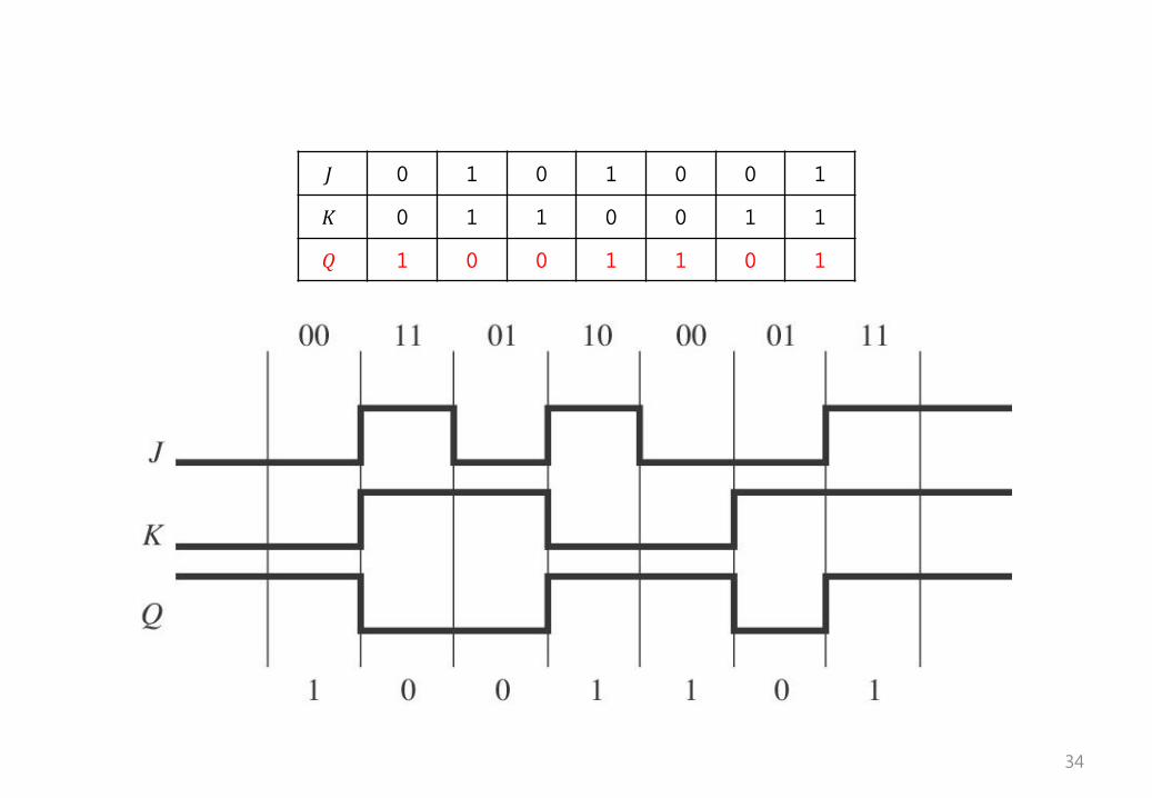
𝐽 0 1 0 1 0 0 1
𝐾 0 1 1 0 0 1 1
𝑄 1 0 0 1 1 0 1
34
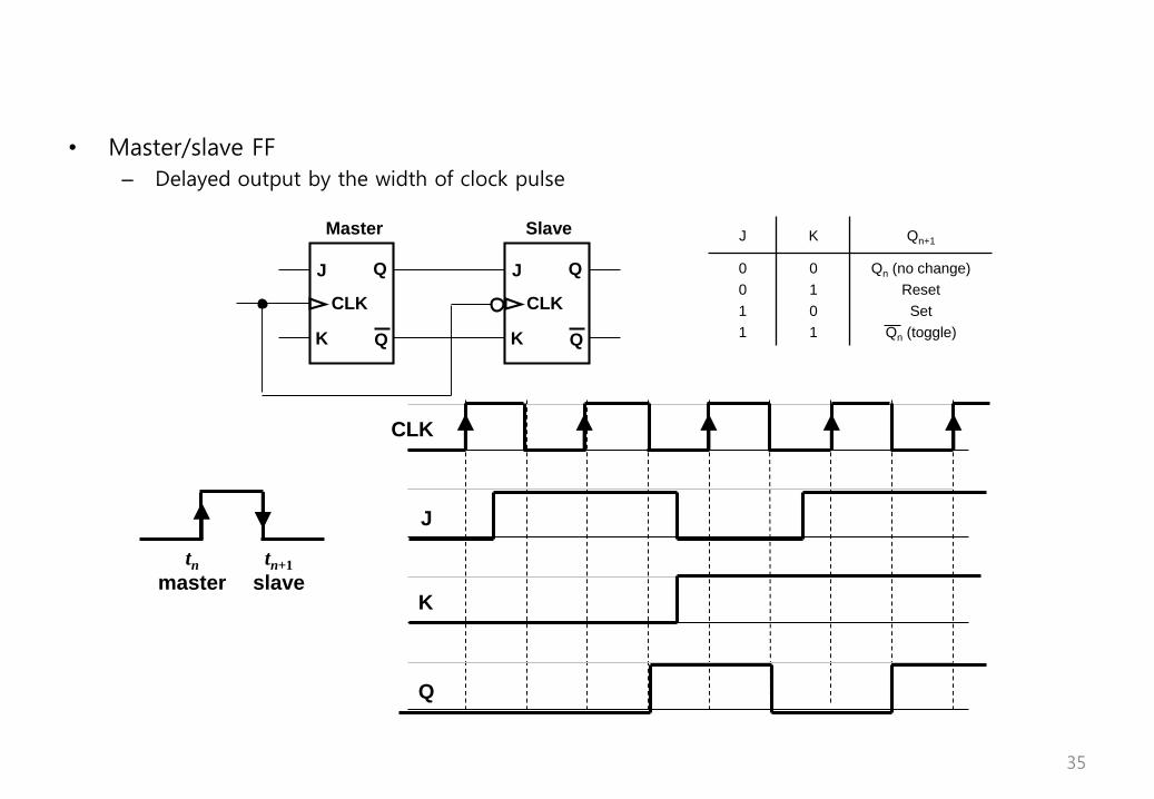
• Master/slave FF
– Delayed output by the width of clock pulse
35
J
K
Q
Q
CLK
J
K
Q
Q
CLK
Master Slave
J
K
Q
CLK
tnmaster
tn+1
slave
J K Qn+1
0
0
1
1
0
1
0
1
Qn (no change)
Reset
Set
Qn (toggle)
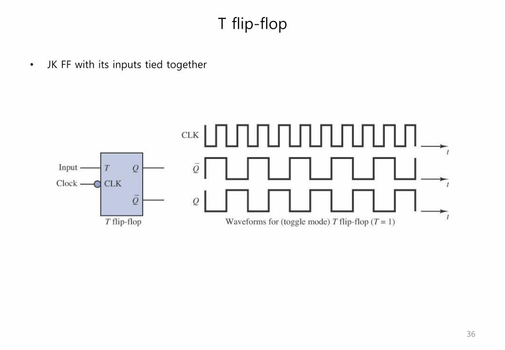
• JK FF with its inputs tied together
T flip-flop
36
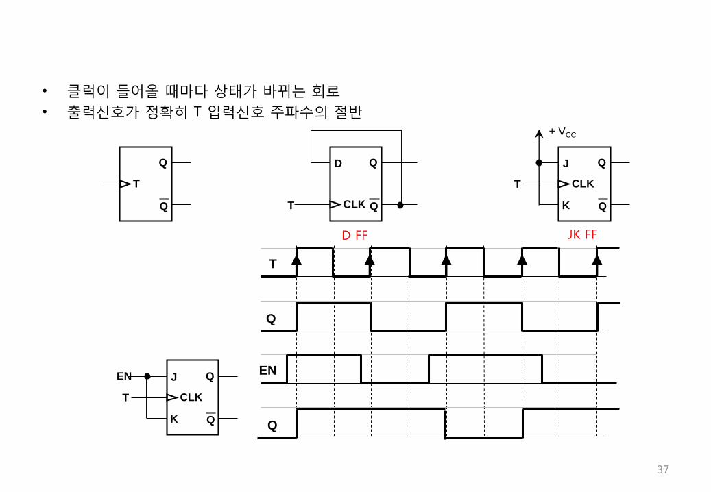
• 클럭이 들어올 때마다 상태가 바뀌는 회로
• 출력신호가 정확히 T 입력신호 주파수의 절반
37
Q
Q
T
D Q
QCLKT
J
K
Q
Q
CLKT
+ VCC
J
K
Q
Q
CLKT
EN
Q
EN
Q
T
D FF JK FF
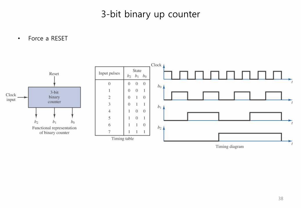
• Force a RESET
3-bit binary up counter
38
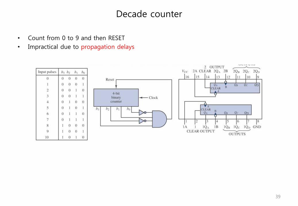
• Count from 0 to 9 and then RESET
• Impractical due to propagation delays
Decade counter
39
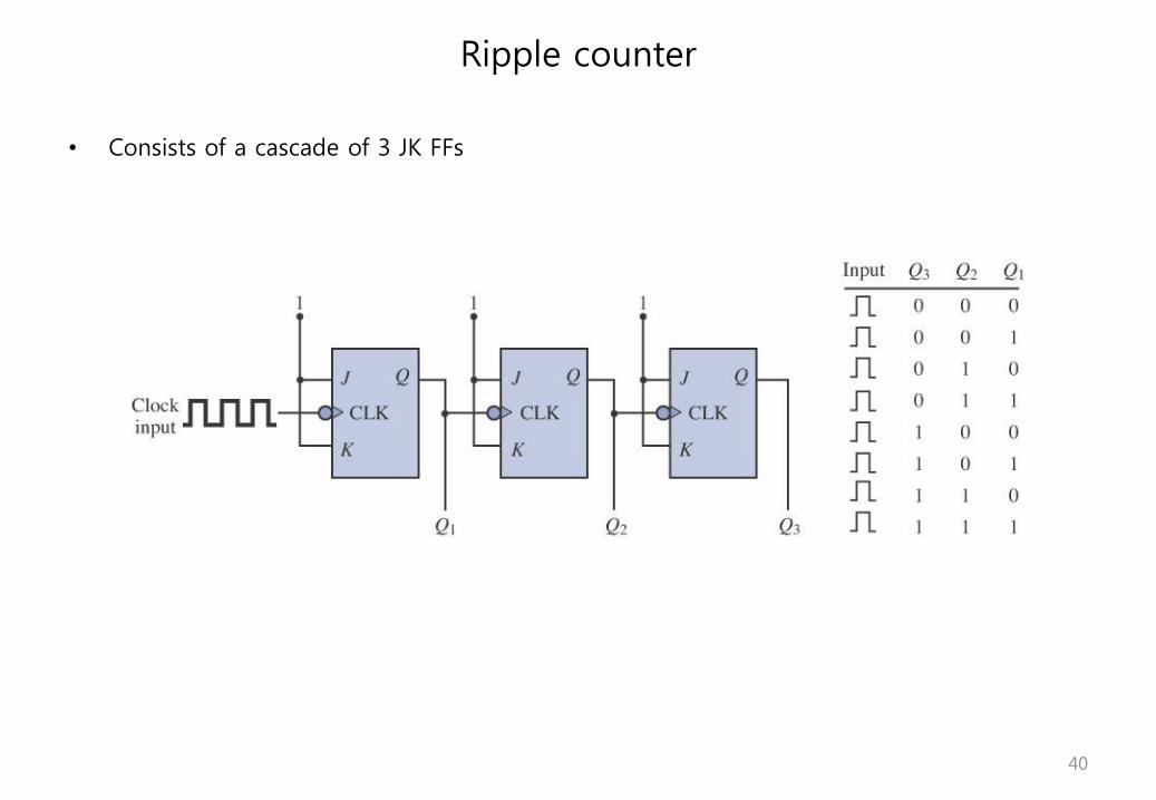
• Consists of a cascade of 3 JK FFs
Ripple counter
40
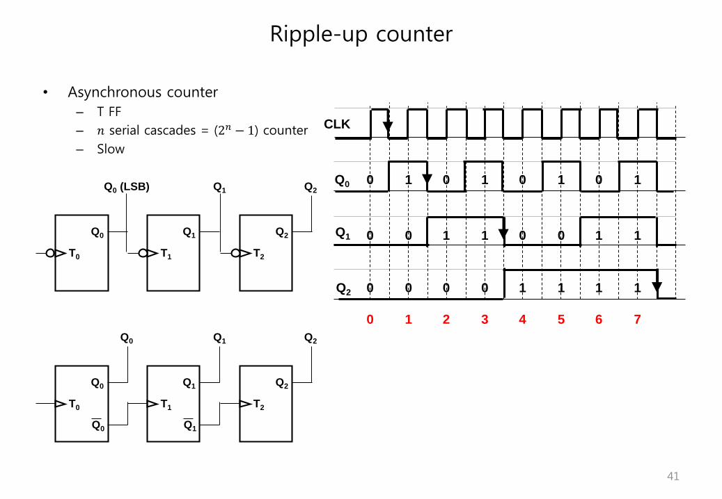
• Asynchronous counter
– T FF
– 𝑛 serial cascades = (2𝑛 − 1) counter
– Slow
Ripple-up counter
41
Q0
T0
Q1
T1
Q2
T2
Q0 (LSB) Q1 Q2
Q0
Q1
Q2
CLK
0
0
0
0
1
0
0
1
0
1
0
2
1
1
0
3
0
0
1
4
1
0
1
5
0
1
1
6
1
1
1
7
Q0
T0
Q1
T1
Q2
T2
Q0 Q1 Q2
Q0 Q1
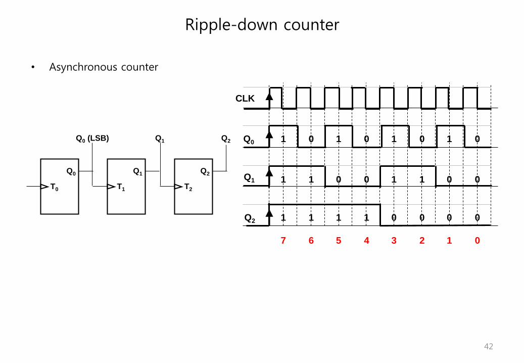
• Asynchronous counter
Ripple-down counter
42
Q0
T0
Q1
T1
Q2
T2
Q0 (LSB) Q1 Q2 Q0
Q1
Q2
CLK
1
1
1
7
0
1
1
6
1
0
1
5
0
0
1
4
1
1
0
3
0
1
0
2
1
0
0
1
0
0
0
0
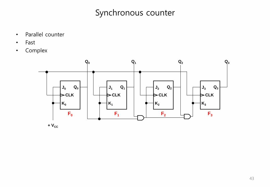
• Parallel counter
• Fast
• Complex
Synchronous counter
43
J0
K0
Q0
CLK
+ VCC
J1
K1
Q1
CLK
J2
K2
Q2
CLK
J3
K3
Q3
CLK
Q0 Q1 Q2 Q3
F0 F1 F2 F3
44
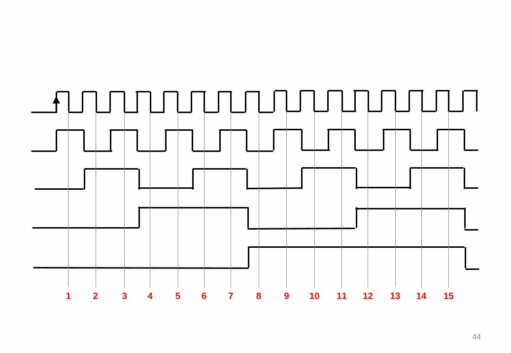
1 2 3 4 5 6 7 8 9 10 11 12 13 14 15
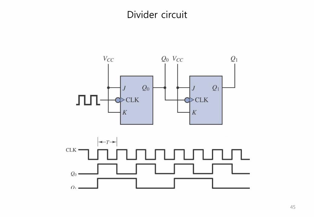
Divider circuit
45
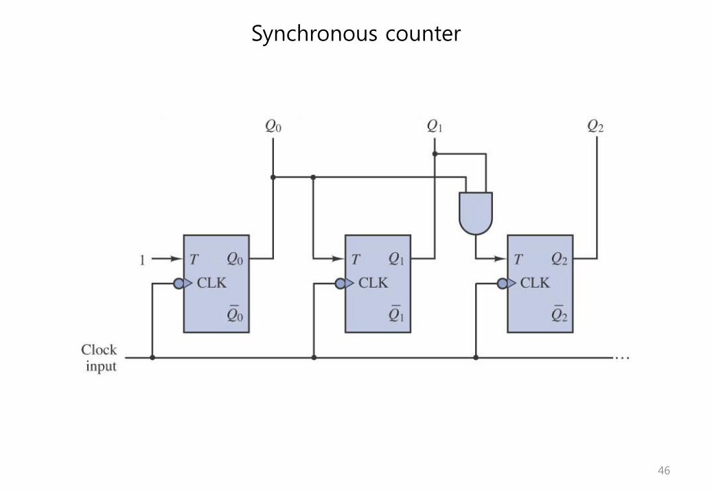
Synchronous counter
46
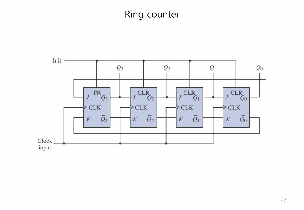
Ring counter
47
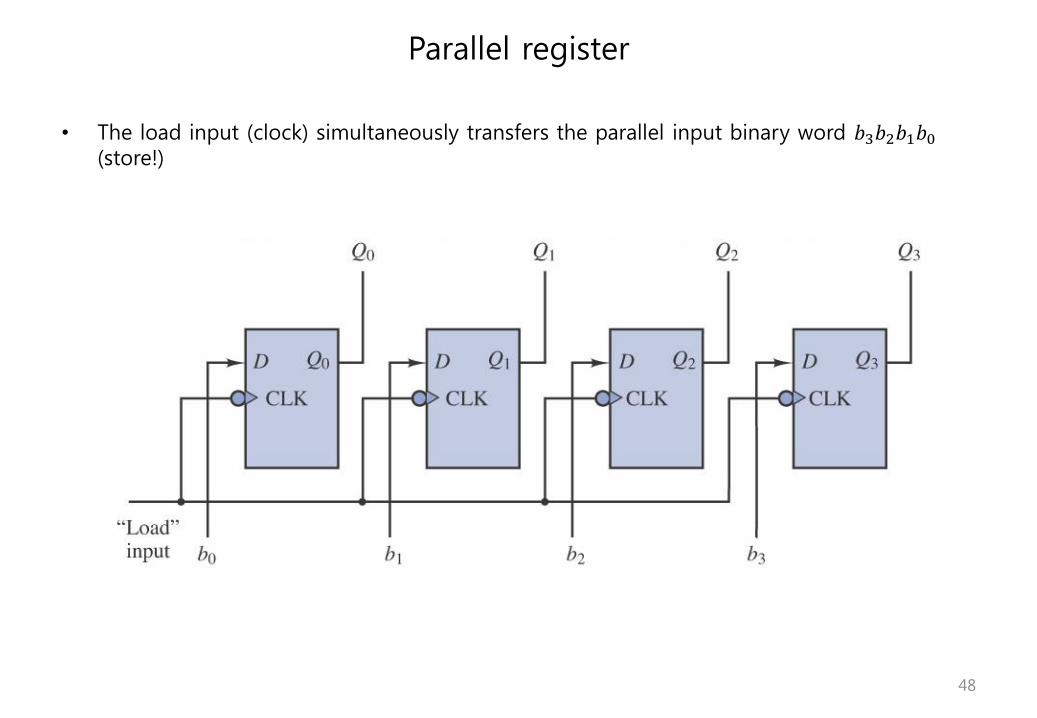
• The load input (clock) simultaneously transfers the parallel input binary word 𝑏3𝑏2𝑏1𝑏0
(store!)
Parallel register
48
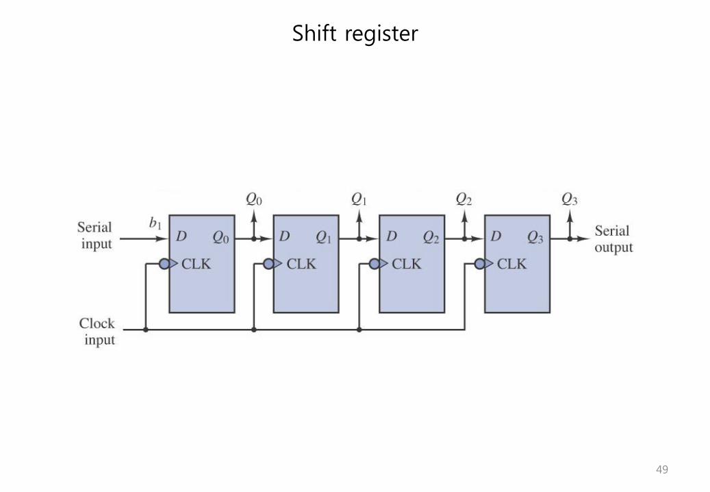
Shift register
49
Related Documents