EE 330 Lecture 6 • Complex Logic Gates • Pass Transistor Logic • Improved Switch-Level Model

Welcome message from author
This document is posted to help you gain knowledge. Please leave a comment to let me know what you think about it! Share it to your friends and learn new things together.
Transcript
EE 330
Lecture 6
• Complex Logic Gates
• Pass Transistor Logic
• Improved Switch-Level Model
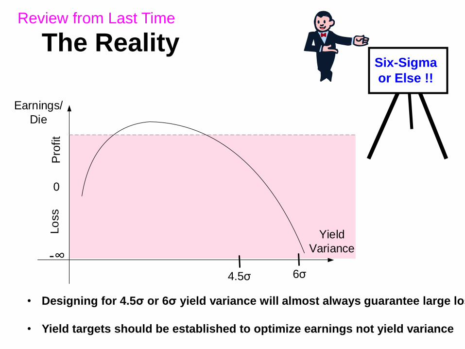
Six-Sigma
or Else !!
The Reality
Earnings/
Die
0
Lo
ss
Pro
fit
-∞6σ
Yield
Variance
4.5σ
• Designing for 4.5σ or 6σ yield variance will almost always guarantee large losses
• Yield targets should be established to optimize earnings not yield variance
Review from Last Time
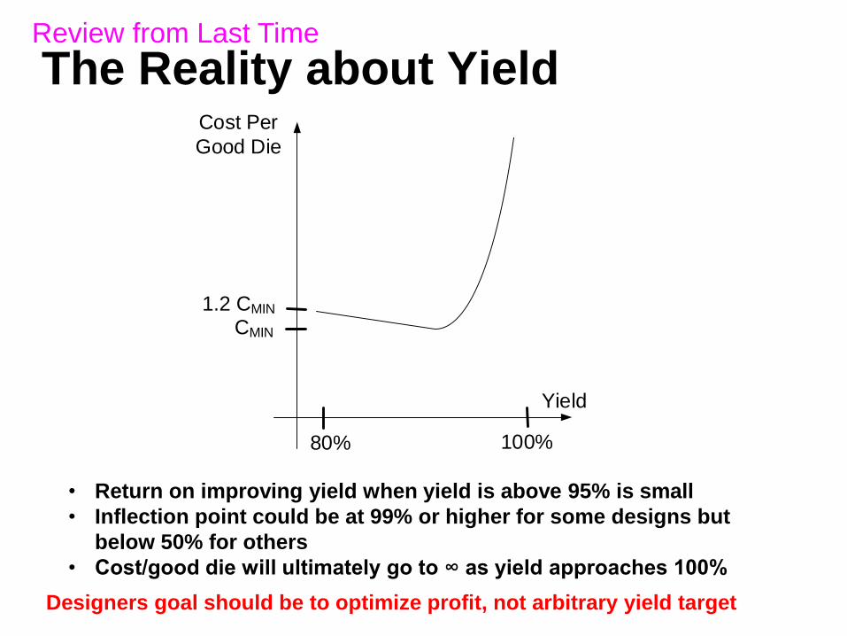
The Reality about Yield
• Return on improving yield when yield is above 95% is small
• Inflection point could be at 99% or higher for some designs but
below 50% for others
• Cost/good die will ultimately go to ∞ as yield approaches 100%
100%80%
CMIN
1.2 CMIN
Cost Per
Good Die
Yield
Designers goal should be to optimize profit, not arbitrary yield target
Review from Last Time
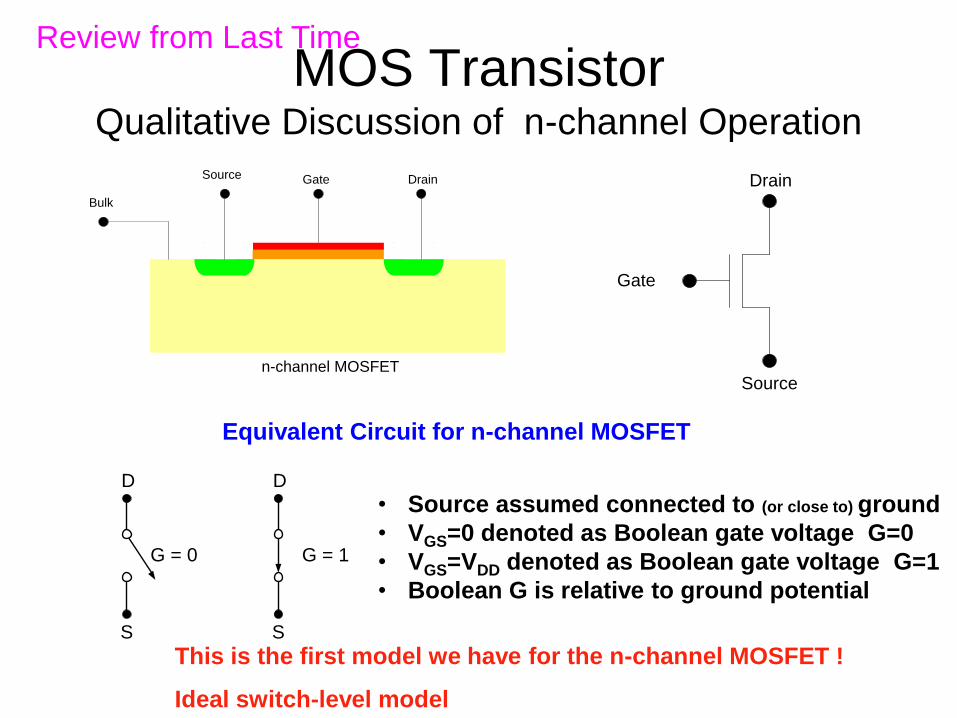
MOS TransistorQualitative Discussion of n-channel Operation
Gate DrainSource
Bulk
n-channel MOSFET
Drain
Gate
Source
D
S
G = 0
D
S
G = 1
Equivalent Circuit for n-channel MOSFET
This is the first model we have for the n-channel MOSFET !
Ideal switch-level model
• Source assumed connected to (or close to) ground
• VGS=0 denoted as Boolean gate voltage G=0
• VGS=VDD denoted as Boolean gate voltage G=1
• Boolean G is relative to ground potential
Review from Last Time
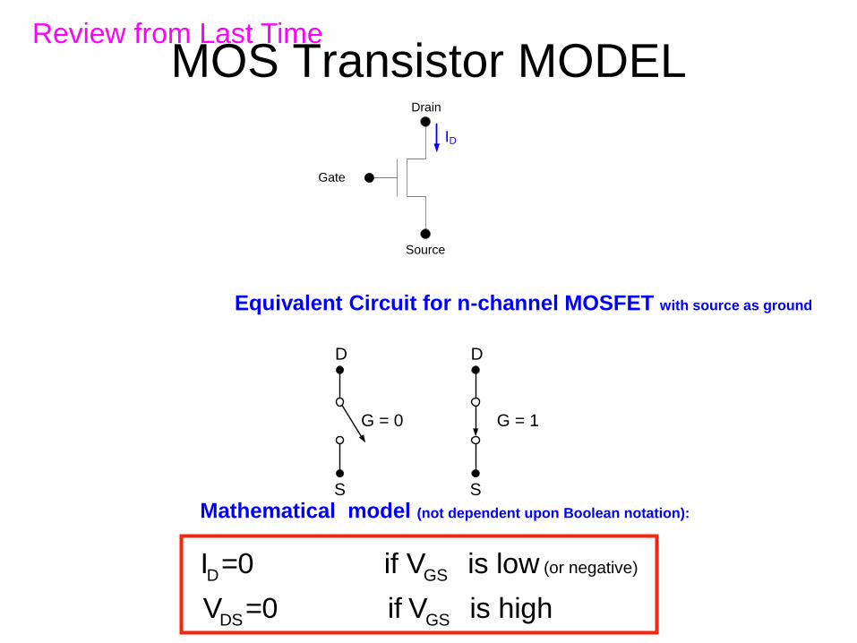
MOS Transistor MODELDrain
Gate
Source
ID
D
S
G = 0
D
S
G = 1
Equivalent Circuit for n-channel MOSFET with source as ground
(or negative)D GS
DS GS
I =0 if V is low
V =0 if V is high
Mathematical model (not dependent upon Boolean notation):
Review from Last Time
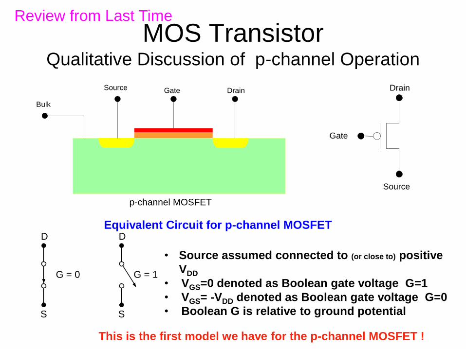
MOS TransistorQualitative Discussion of p-channel Operation
Gate DrainSource
Bulk
p-channel MOSFET
Drain
Gate
Source
Equivalent Circuit for p-channel MOSFETD
S
G = 1
D
S
G = 0
This is the first model we have for the p-channel MOSFET !
• Source assumed connected to (or close to) positive
VDD
• VGS=0 denoted as Boolean gate voltage G=1
• VGS= -VDD denoted as Boolean gate voltage G=0
• Boolean G is relative to ground potential
Review from Last Time
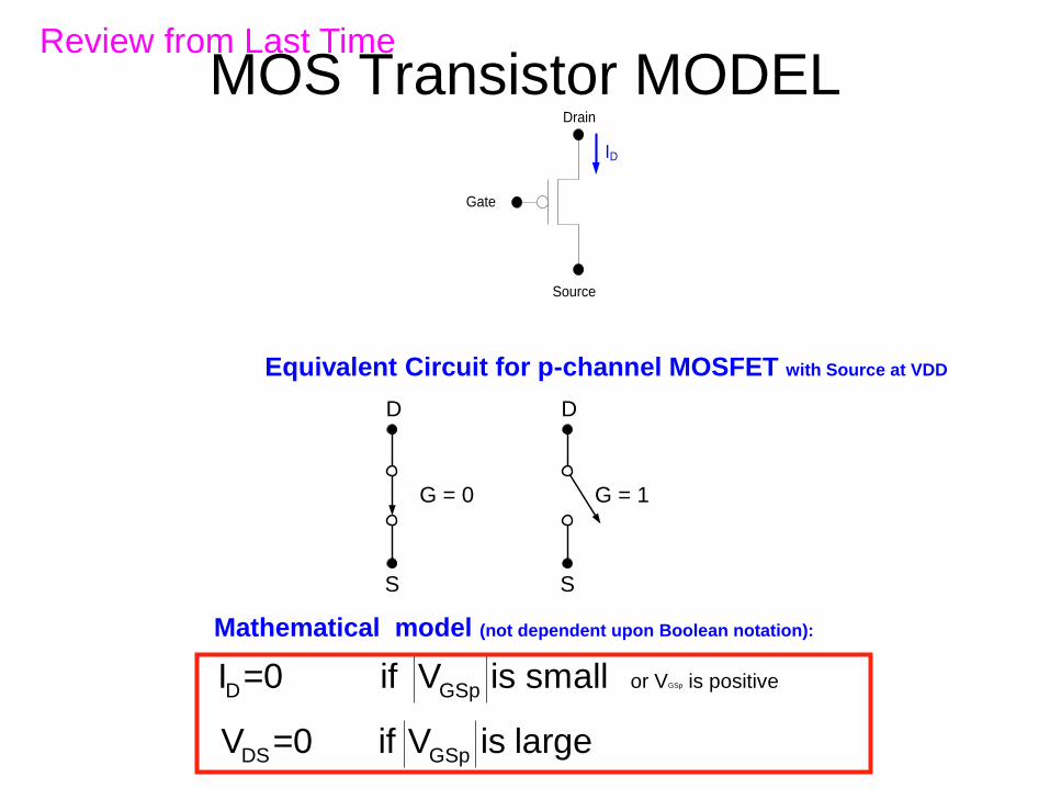
MOS Transistor MODEL
Equivalent Circuit for p-channel MOSFET with Source at VDD
GSpor V is positiveD GSp
DS GSp
I =0 if V is small
V =0 if V is large
Drain
Gate
Source
ID
D
S
G = 1
D
S
G = 0
Mathematical model (not dependent upon Boolean notation):
Review from Last Time
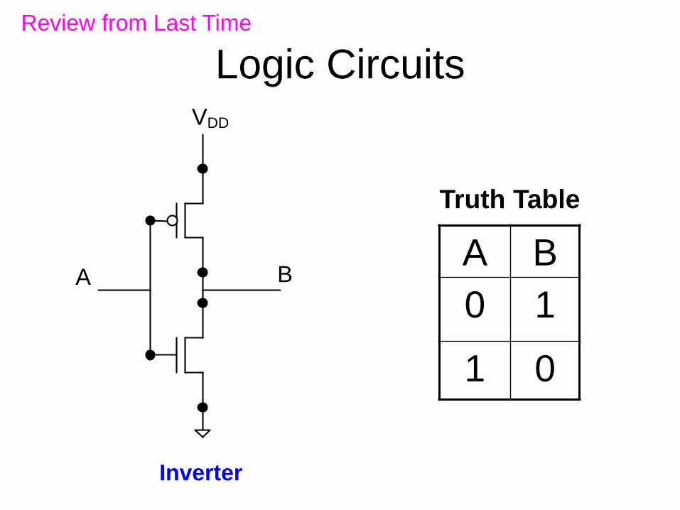
Logic CircuitsVDD
A B
Inverter
A B
0 1
1 0
Truth Table
Review from Last Time
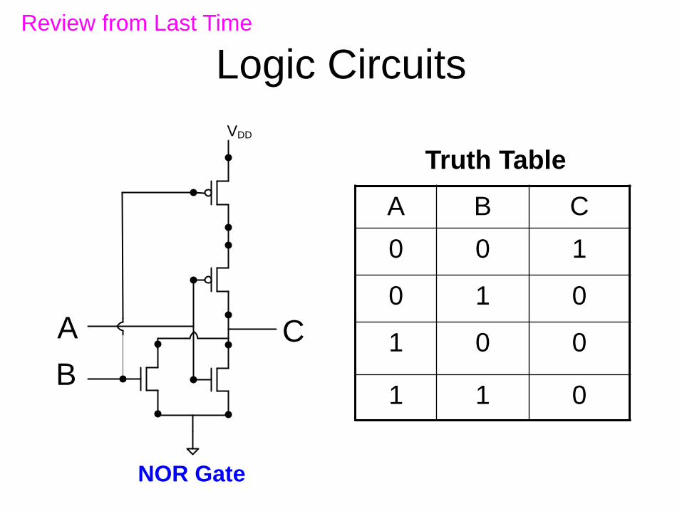
Logic Circuits
A B C
0 0 1
0 1 0
1 0 0
1 1 0
Truth Table
NOR Gate
A
B
C
VDD
Review from Last Time
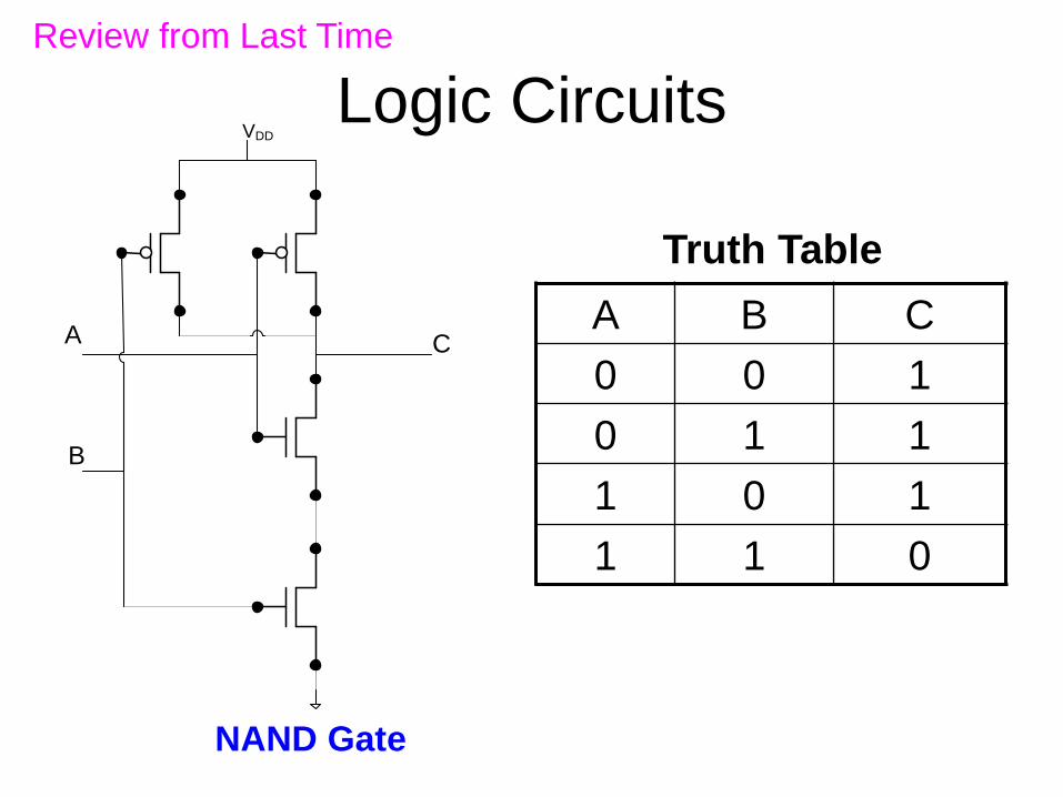
Logic Circuits
A B C
0 0 1
0 1 1
1 0 1
1 1 0
Truth Table
NAND Gate
VDD
A
B
C
Review from Last Time
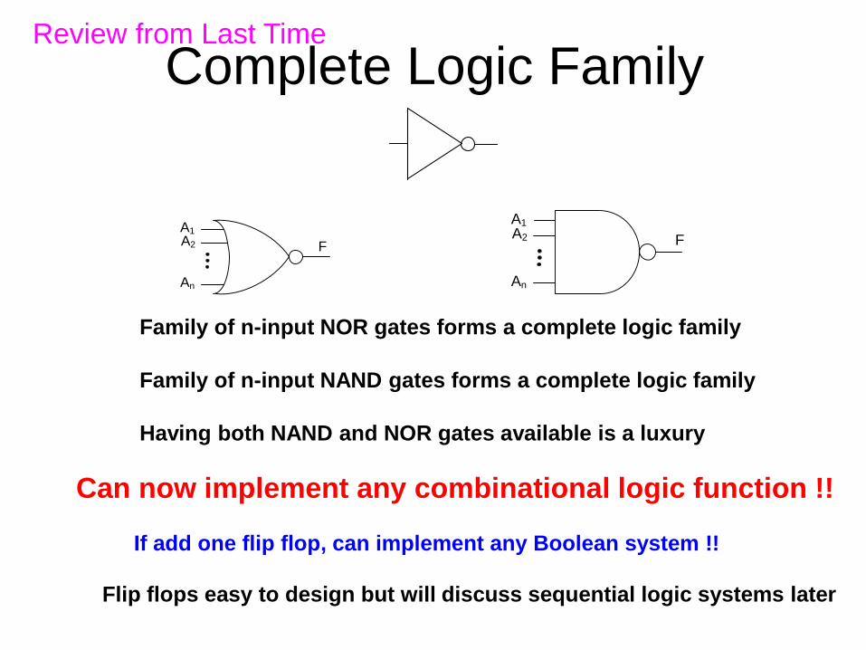
Complete Logic Family
A1
A2
An
F
A1
A2
An
F
Family of n-input NOR gates forms a complete logic family
Family of n-input NAND gates forms a complete logic family
Having both NAND and NOR gates available is a luxury
Can now implement any combinational logic function !!
If add one flip flop, can implement any Boolean system !!
Flip flops easy to design but will discuss sequential logic systems later
Review from Last Time
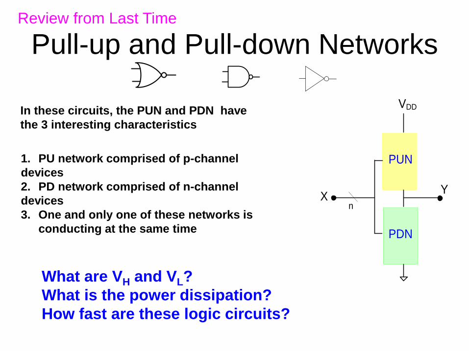
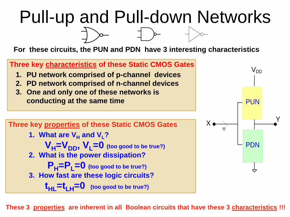
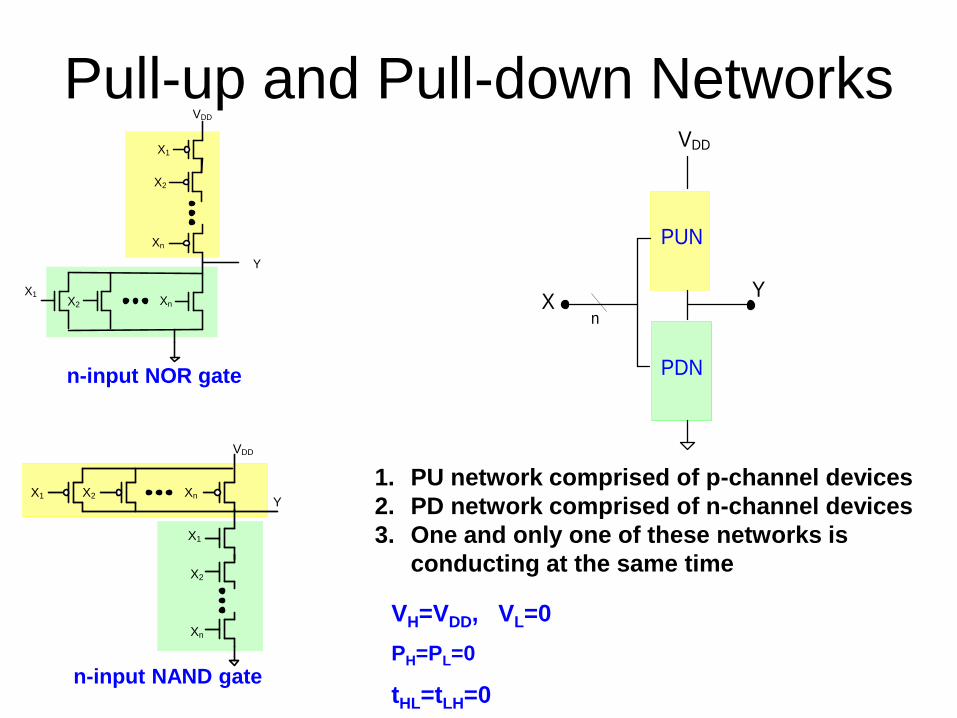
Pull-up and Pull-down Networks
1. PU network comprised of p-channel
devices
2. PD network comprised of n-channel
devices
3. One and only one of these networks is
conducting at the same time
VDD
XY
PUN
PDN
n
What are VH and VL?
What is the power dissipation?
How fast are these logic circuits?
In these circuits, the PUN and PDN have
the 3 interesting characteristics
Review from Last Time
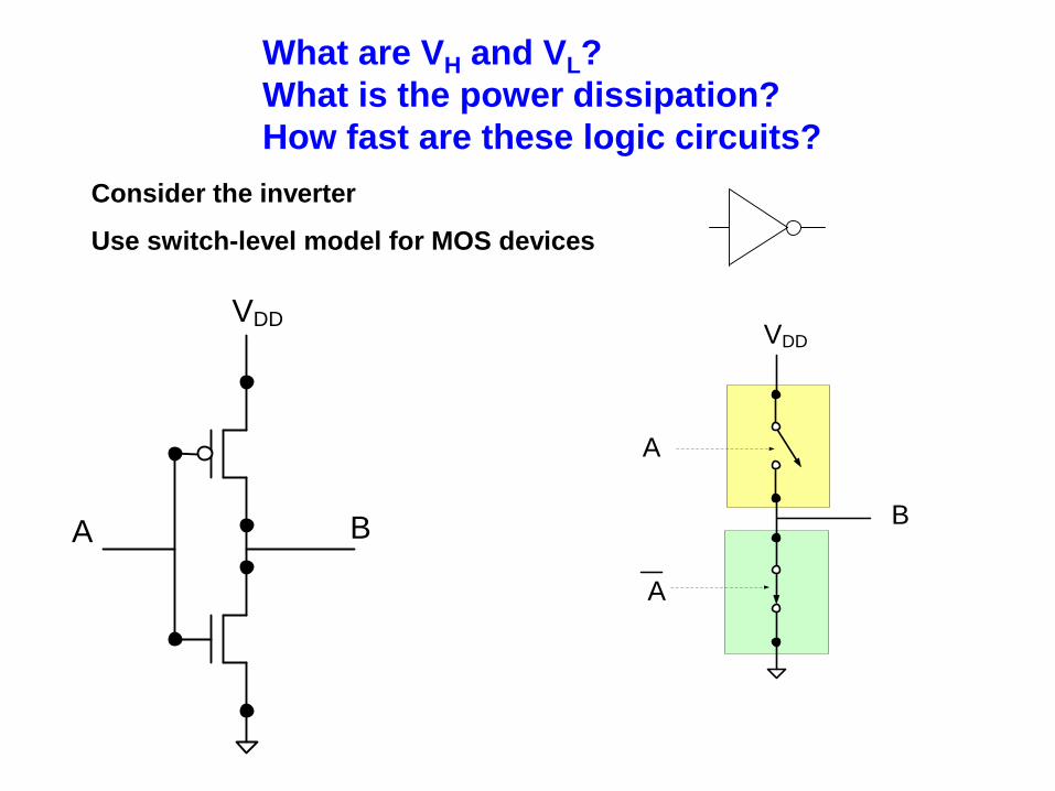
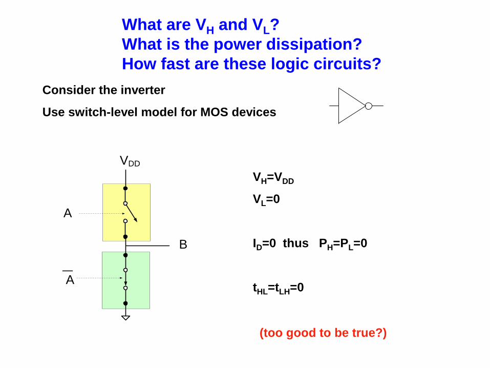
VDD
A B
VDD
A
B
A
What are VH and VL?
What is the power dissipation?
How fast are these logic circuits?
Consider the inverter
Use switch-level model for MOS devices
VDD
A
B
A
What are VH and VL?
What is the power dissipation?
How fast are these logic circuits?
Consider the inverter
Use switch-level model for MOS devices
VH=VDD
VL=0
ID=0 thus PH=PL=0
tHL=tLH=0
(too good to be true?)
Pull-up and Pull-down Networks
1. PU network comprised of p-channel devices
2. PD network comprised of n-channel devices
3. One and only one of these networks is
conducting at the same time
VDD
XY
PUN
PDN
n
1. What are VH and VL?
VH=VDD, VL=0 (too good to be true?)
2. What is the power dissipation?
PH=PL=0 (too good to be true?)
3. How fast are these logic circuits?
tHL=tLH=0 (too good to be true?)
These 3 properties are inherent in all Boolean circuits that have these 3 characteristics !!!
For these circuits, the PUN and PDN have 3 interesting characteristics
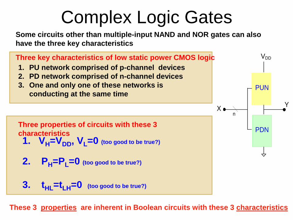
Three key characteristics of these Static CMOS Gates
Three key properties of these Static CMOS Gates
Pull-up and Pull-down Networks
1. PU network comprised of p-channel devices
2. PD network comprised of n-channel devices
3. One and only one of these networks is
conducting at the same time
VDD
XY
PUN
PDN
n
1. VH=VDD, VL=0 (too good to be true?)
2. PH=PL=0 (too good to be true?)
3. tHL=tLH=0 (too good to be true?)
These 3 properties are inherent in Boolean circuits with these 3 characteristics
Three key characteristics of Static CMOS Gates
Three properties of Static CMOS Gates (based
upon simple switch-level model)
Pull-up and Pull-down Networks
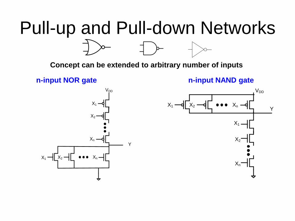
Concept can be extended to arbitrary number of inputs
VDD
X2 Xn
X1
X2
Xn Y
X1
n-input NOR gate
VDD
X2
Xn X1 X2
Xn
Y
X1
n-input NAND gate
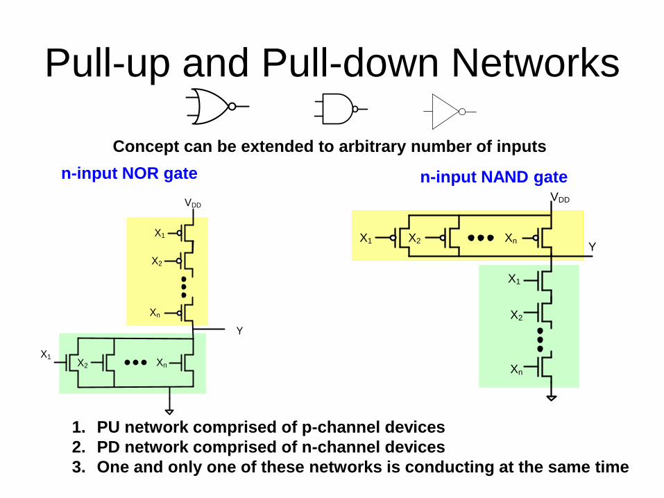
Pull-up and Pull-down Networks
1. PU network comprised of p-channel devices
2. PD network comprised of n-channel devices
3. One and only one of these networks is conducting at the same time
Concept can be extended to arbitrary number of inputs
VDD
X2 Xn
X1
X2
Xn
Y
X1
n-input NOR gate
VDD
X2
Xn X1 X2
Xn
Y
X1
n-input NAND gate
Pull-up and Pull-down Networks
1. PU network comprised of p-channel devices
2. PD network comprised of n-channel devices
3. One and only one of these networks is
conducting at the same time
VDD
X2 Xn
X1
X2
Xn
Y
X1
n-input NOR gate
VDD
X2
Xn X1 X2
Xn
Y
X1
n-input NAND gate
VDD
XY
PUN
PDN
n
VH=VDD, VL=0
PH=PL=0
tHL=tLH=0
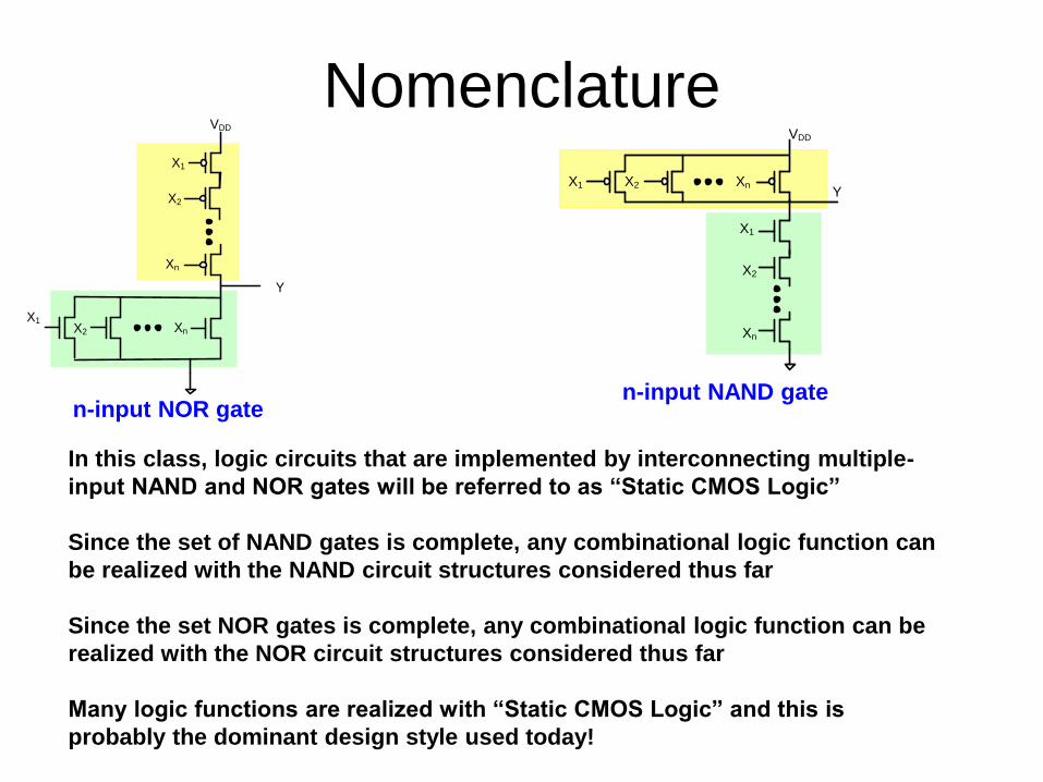
Nomenclature VDD
X2 Xn
X1
X2
Xn
Y
X1
n-input NOR gate
VDD
X2
Xn X1 X2
Xn
Y
X1
n-input NAND gate
In this class, logic circuits that are implemented by interconnecting multiple-
input NAND and NOR gates will be referred to as “Static CMOS Logic”
Since the set of NAND gates is complete, any combinational logic function can
be realized with the NAND circuit structures considered thus far
Since the set NOR gates is complete, any combinational logic function can be
realized with the NOR circuit structures considered thus far
Many logic functions are realized with “Static CMOS Logic” and this is
probably the dominant design style used today!
Example 1:
How many transistors are required to realize the
function
in a basic CMOS process if static NAND and NOR
gates are used? Assume A, B and C are available.
CABAF
Circuit Structures
Circuit Design
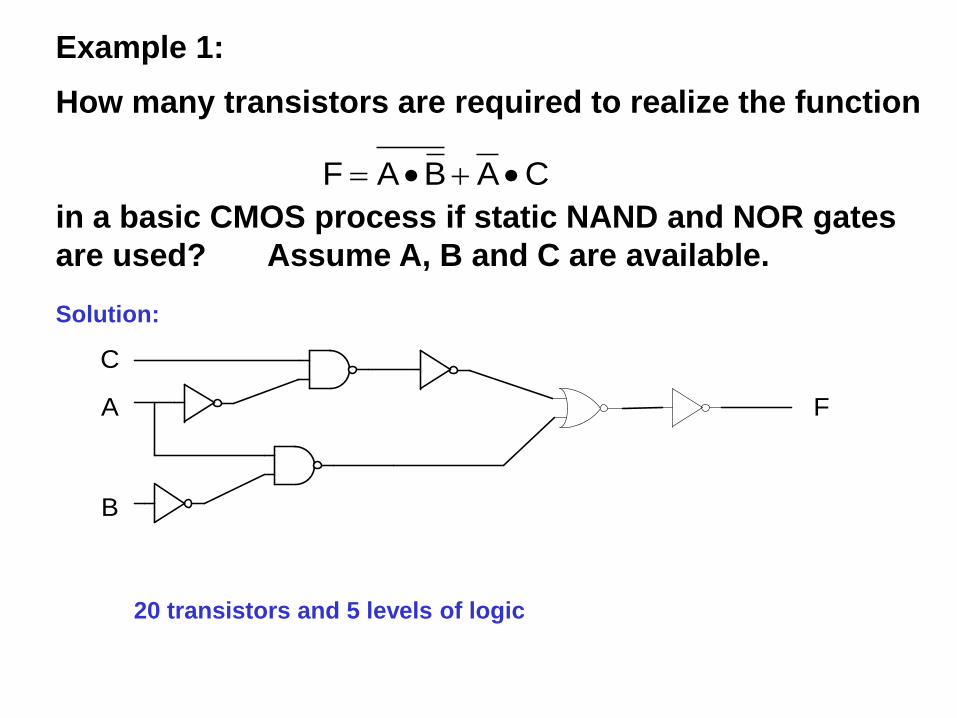
How many transistors are required to realize the function
in a basic CMOS process if static NAND and NOR gates
are used? Assume A, B and C are available.
CABAF
Solution:
C
A F
B
20 transistors and 5 levels of logic
Example 1:
How many transistors are required to realize the function
in a basic CMOS process if static NAND and NOR gates
are used? Assume A, B and C are available.
CABAF
Solution (alternative): From basic Boolean Manipulations
CACAF BABA
BABC1AF
A
BF
8 transistors and 3 levels of logic
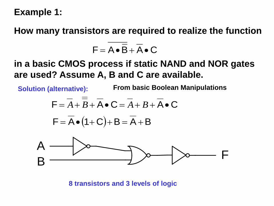
Example 1:
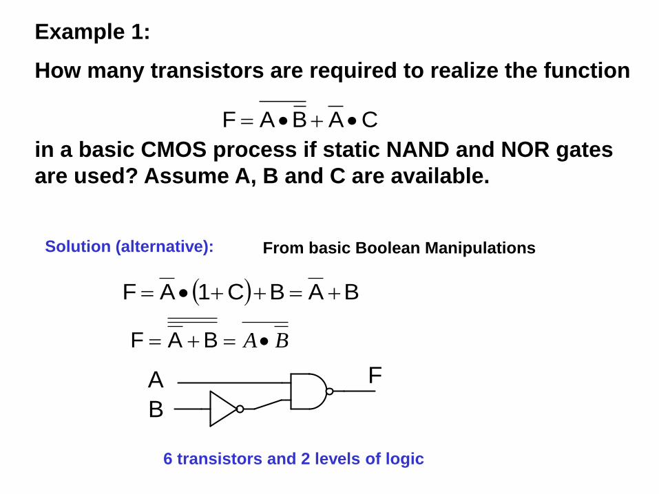
How many transistors are required to realize the function
in a basic CMOS process if static NAND and NOR gates
are used? Assume A, B and C are available.
CABAF
Solution (alternative): From basic Boolean Manipulations
BABC1AF
BA BAF
A
B
F
6 transistors and 2 levels of logic
Example 1:
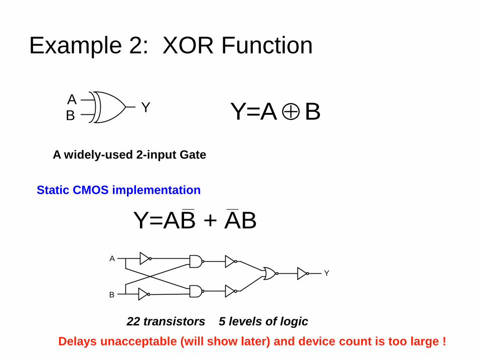
Example 2: XOR Function
AB
Y Y=A B
Y=AB + AB
A
Y
B
A widely-used 2-input Gate
Static CMOS implementation
22 transistors 5 levels of logic
Delays unacceptable (will show later) and device count is too large !
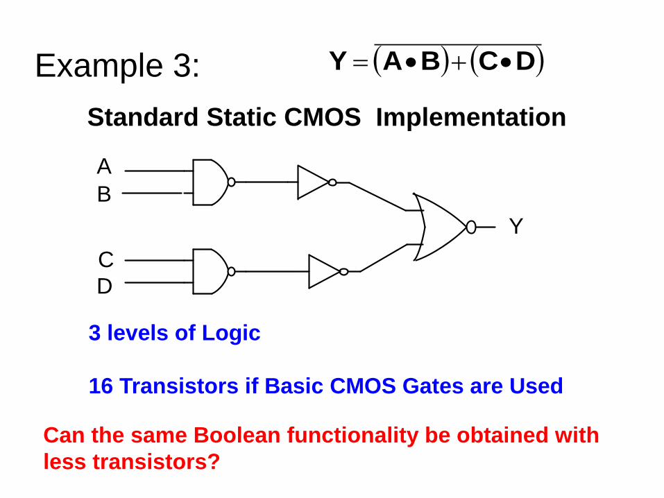
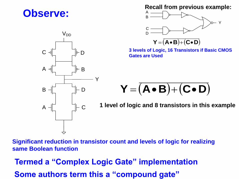
Example 3: DCBAY
A
B
C
D
Y
Standard Static CMOS Implementation
3 levels of Logic
16 Transistors if Basic CMOS Gates are Used
Can the same Boolean functionality be obtained with
less transistors?
Complex Logic Gates
1. PU network comprised of p-channel devices
2. PD network comprised of n-channel devices
3. One and only one of these networks is
conducting at the same time
VDD
XY
PUN
PDN
n
1. VH=VDD, VL=0 (too good to be true?)
2. PH=PL=0 (too good to be true?)
3. tHL=tLH=0 (too good to be true?)
These 3 properties are inherent in Boolean circuits with these 3 characteristics
Three key characteristics of low static power CMOS logic
Three properties of circuits with these 3
characteristics
Some circuits other than multiple-input NAND and NOR gates can also
have the three key characteristics
DCBAY
VDD
A
B
C
D
A
C
B
D
Y
Observe:
Significant reduction in transistor count and levels of logic for realizing
same Boolean function
Termed a “Complex Logic Gate” implementation
Some authors term this a “compound gate”
A
B
C
D
Y
DCBAY
Recall from previous example:
3 levels of Logic, 16 Transistors if Basic CMOS
Gates are Used
1 level of logic and 8 transistors in this example
Complex Logic Gates
Pull-up Network
Pull-down
Network
DCBAY
VDD
A
B
C
D
A
C
B
D
Y
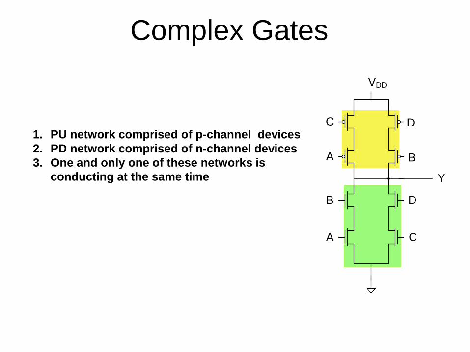
Complex Gates
VDD
A
B
C
D
A
C
B
D
Y
1. PU network comprised of p-channel devices
2. PD network comprised of n-channel devices
3. One and only one of these networks is
conducting at the same time

Complex GatesVDD
XY
PUN
PDN
n
Nomenclature:
When the logic gate shown is not a multiple-input NAND or NOR gate but
has Characteristics 1, 2, and 3 above, the gate will be referred to as a
Complex Logic Gate
Complex Logic Gates also implement static logic functions and some
authors would refer to this as Static CMOS Logic as well but we will make
the distinction and refer to this as “Complex Logic Gates”
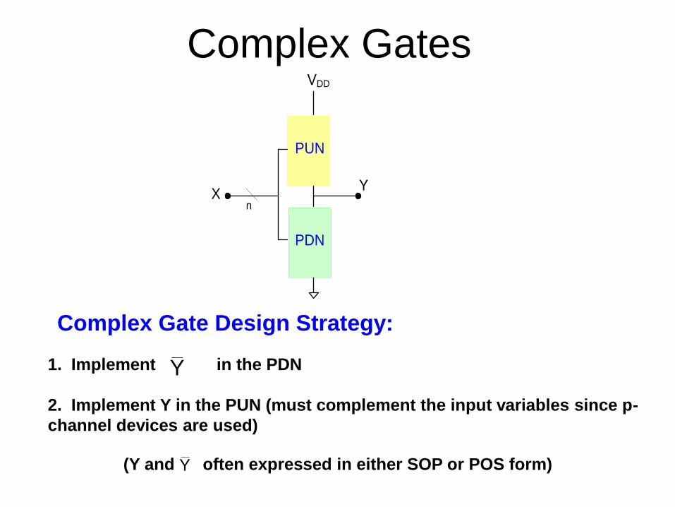
Complex GatesVDD
XY
PUN
PDN
n
1. Implement in the PDN
2. Implement Y in the PUN (must complement the input variables since p-
channel devices are used)
Y
Complex Gate Design Strategy:
(Y and often expressed in either SOP or POS form)Y
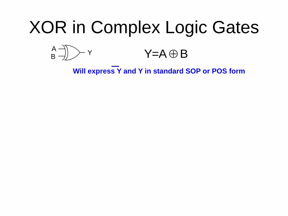
XOR in Complex Logic GatesAB
Y Y=A B
Will express Y and Y in standard SOP or POS form
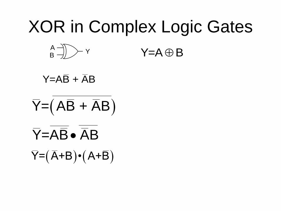
XOR in Complex Logic GatesAB
Y Y=A B
Y=AB + AB
Y= AB + AB
Y=AB AB
Y= A+B • A+B
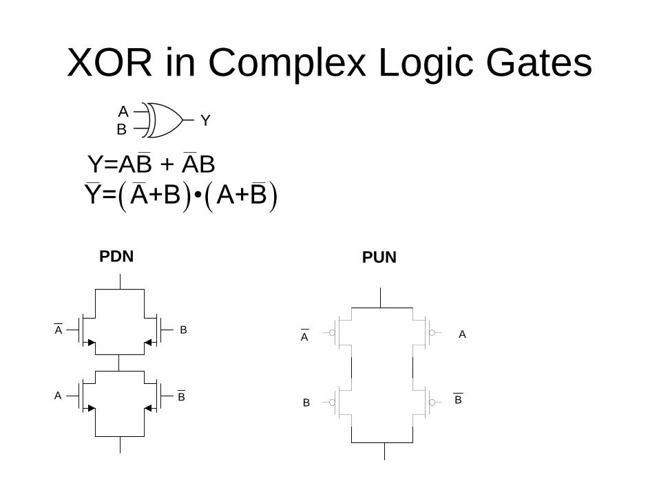
XOR in Complex Logic GatesAB
Y
Y= A+B • A+B
Y=AB + AB
PDN PUN
A
B
A
B
A
A
B
B
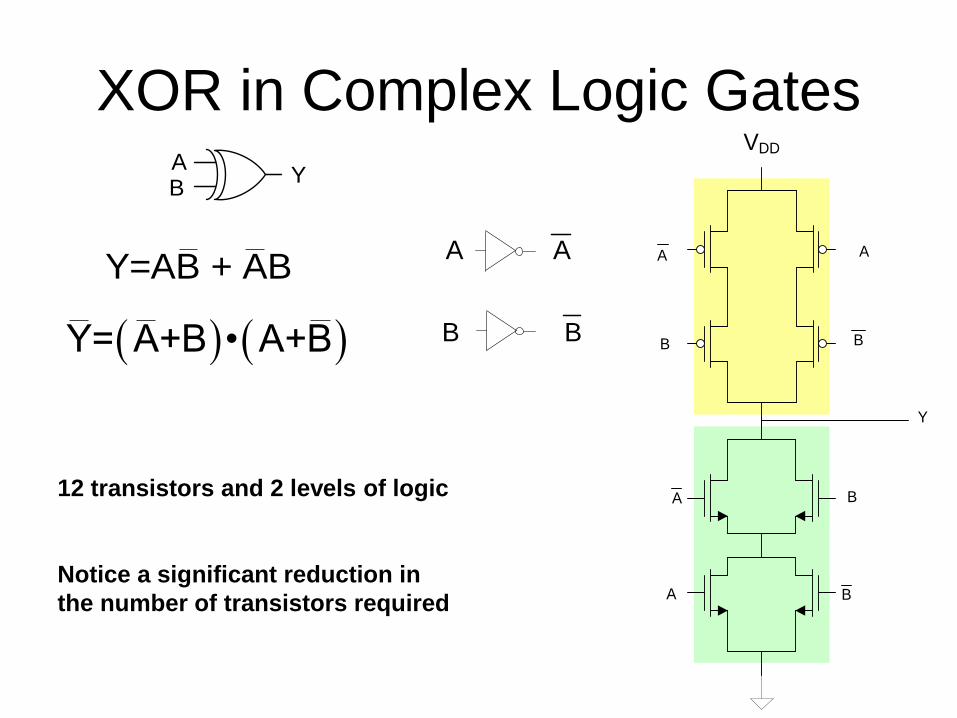
XOR in Complex Logic GatesAB
Y
Y= A+B • A+B
Y=AB + ABA A
BB
12 transistors and 2 levels of logic
Notice a significant reduction in
the number of transistors required
A
A
B
B
A
B
A
B
Y
VDD
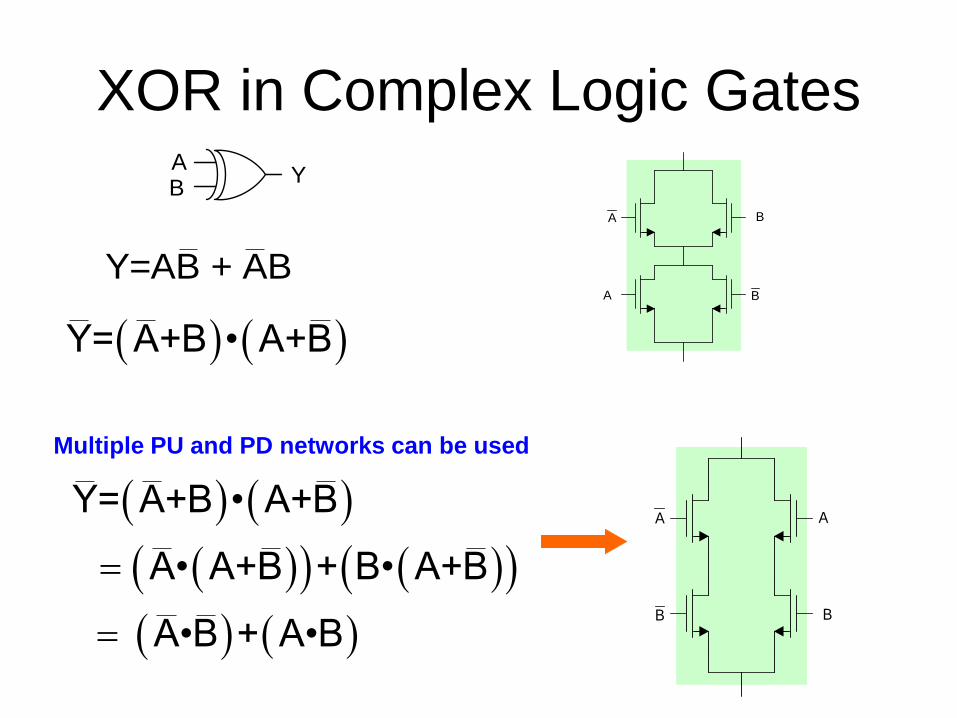
XOR in Complex Logic GatesAB
Y
Y= A+B • A+B
Y=AB + AB
Multiple PU and PD networks can be used
Y= A+B • A+B
A• A+B + B• A+B
A•B + A•B
A
A
B
B
A A
BB
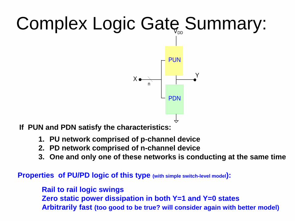
Complex Logic Gate Summary:
1. PU network comprised of p-channel device
2. PD network comprised of n-channel device
3. One and only one of these networks is conducting at the same time
VDD
XY
PUN
PDN
n
Properties of PU/PD logic of this type (with simple switch-level model):
Rail to rail logic swings
Zero static power dissipation in both Y=1 and Y=0 states
Arbitrarily fast (too good to be true? will consider again with better model)
If PUN and PDN satisfy the characteristics:
• Pass Transistor Logic
• Improved Switch-Level Model
• Propagation Delay
• Stick Diagrams
• Technology Files
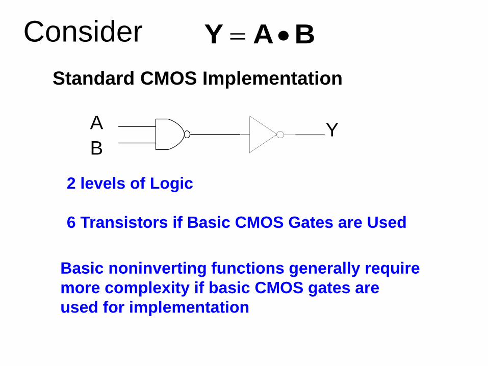
Consider
Standard CMOS Implementation
2 levels of Logic
6 Transistors if Basic CMOS Gates are Used
BAY
A
BY
Basic noninverting functions generally require
more complexity if basic CMOS gates are
used for implementation
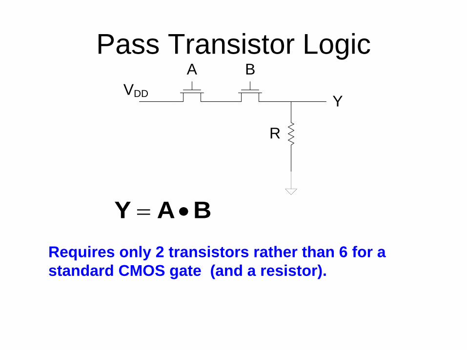
Pass Transistor Logic
VDD
A B
Y
R
BAY
Requires only 2 transistors rather than 6 for a
standard CMOS gate (and a resistor).
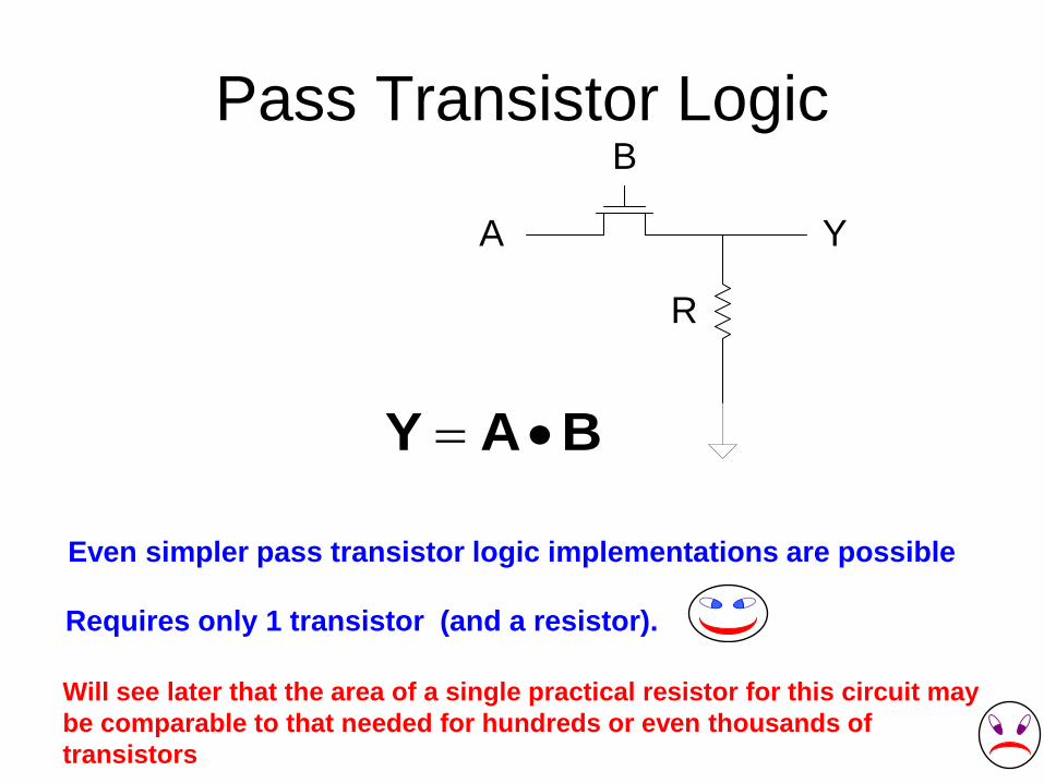
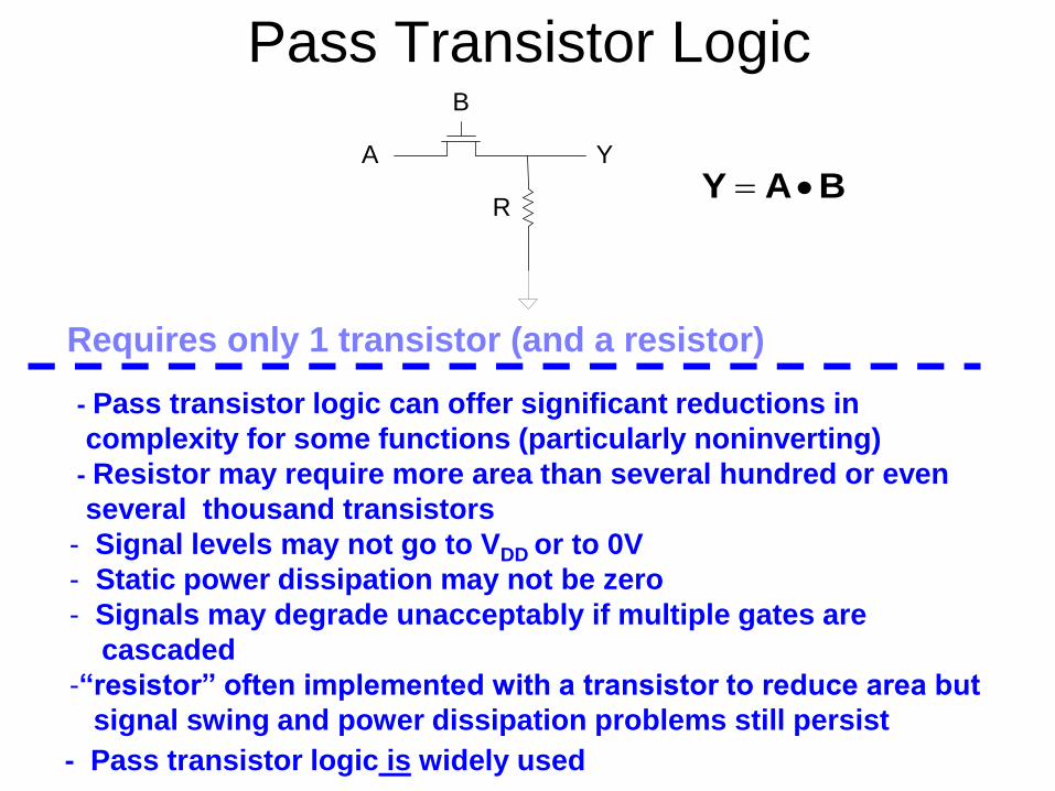
Pass Transistor Logic
BAY
Requires only 1 transistor (and a resistor).
A
B
Y
R
Even simpler pass transistor logic implementations are possible
Will see later that the area of a single practical resistor for this circuit may
be comparable to that needed for hundreds or even thousands of
transistors
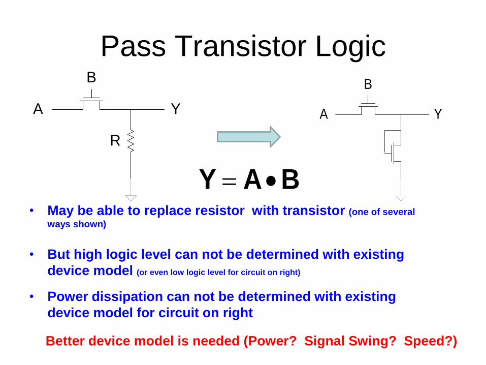
Pass Transistor Logic
BAY • May be able to replace resistor with transistor (one of several
ways shown)
• But high logic level can not be determined with existing
device model (or even low logic level for circuit on right)
• Power dissipation can not be determined with existing
device model for circuit on right
A
B
Y
R
A
B
Y
Better device model is needed (Power? Signal Swing? Speed?)
Pass Transistor Logic
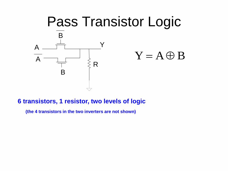
Y A B A
B
Y
RA
B
6 transistors, 1 resistor, two levels of logic
(the 4 transistors in the two inverters are not shown)
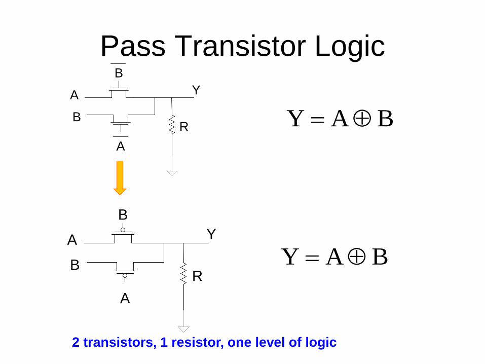
Pass Transistor Logic
Y A B A
B
Y
R
A
B
2 transistors, 1 resistor, one level of logic
A
B
Y
R
A
B Y A B
Pass Transistor Logic
BAY
Requires only 1 transistor (and a resistor)
- Pass transistor logic can offer significant reductions in
complexity for some functions (particularly noninverting)
- Resistor may require more area than several hundred or even
several thousand transistors
- Signal levels may not go to VDD or to 0V
- Static power dissipation may not be zero
- Signals may degrade unacceptably if multiple gates are
cascaded
-“resistor” often implemented with a transistor to reduce area but
signal swing and power dissipation problems still persist
A
B
Y
R
- Pass transistor logic is widely used
Logic Design Styles• Several different logic design styles are often used
throughout a given design (3 considered thus far)– Static CMOS
– Complex Logic Gates
– Pass Transistor Logic
• The designer has complete control over what is placed on silicon and governed only by cost and performance
• New logic design strategies have been proposed recently and others will likely emerge in the future
• The digital designer needs to be familiar with the benefits and limitations of varying logic styles to come up with a good solution for given system requirements
• Pass Transistor Logic
• Improved Switch-Level Model
• Propagation Delay
• Stick Diagrams
• Technology Files
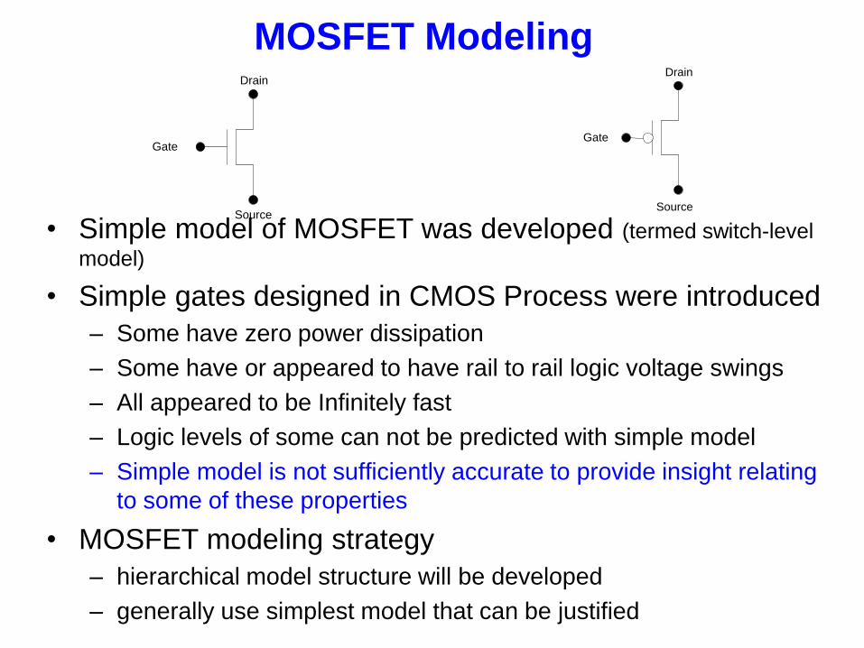
• Simple model of MOSFET was developed (termed switch-level
model)
• Simple gates designed in CMOS Process were introduced
– Some have zero power dissipation
– Some have or appeared to have rail to rail logic voltage swings
– All appeared to be Infinitely fast
– Logic levels of some can not be predicted with simple model
– Simple model is not sufficiently accurate to provide insight relating
to some of these properties
• MOSFET modeling strategy
– hierarchical model structure will be developed
– generally use simplest model that can be justified
MOSFET ModelingDrain
Gate
Source
Drain
Gate
Source
MOS Transistor Models Drain
Gate
Source
Drain
Gate
Source
D
S
G = 1
D
S
G = 0
D
S
G = 0
D
S
G = 1
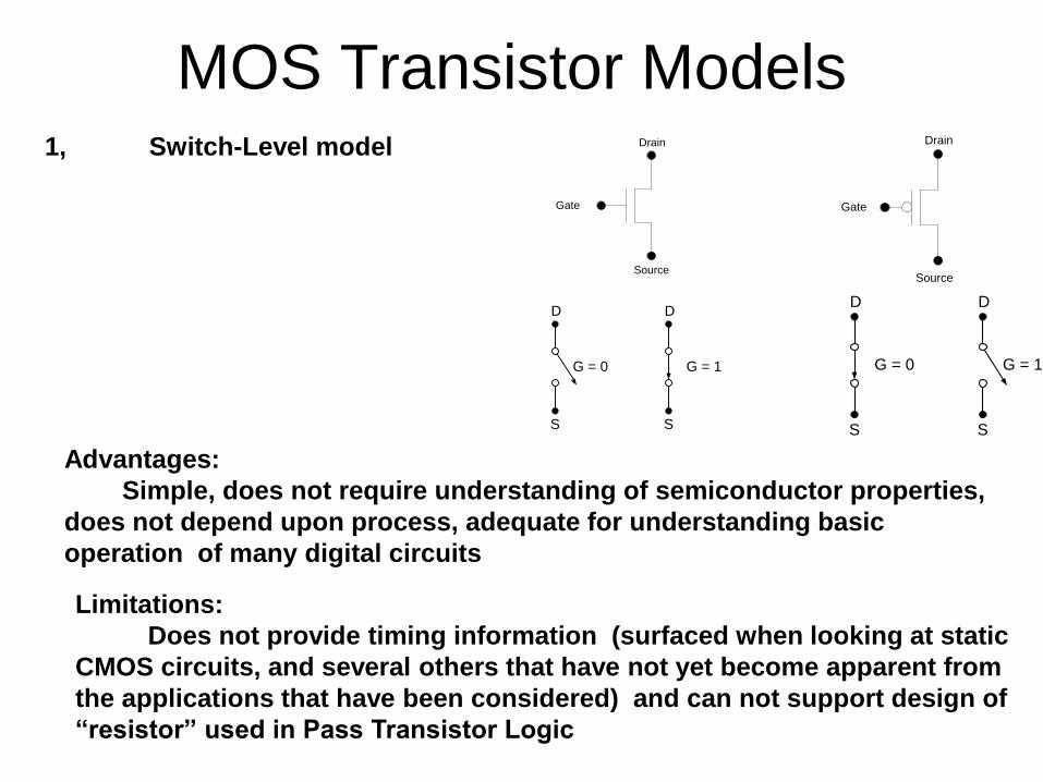
1, Switch-Level model
Advantages:
Simple, does not require understanding of semiconductor properties,
does not depend upon process, adequate for understanding basic
operation of many digital circuits
Limitations:
Does not provide timing information (surfaced when looking at static
CMOS circuits, and several others that have not yet become apparent from
the applications that have been considered) and can not support design of
“resistor” used in Pass Transistor Logic
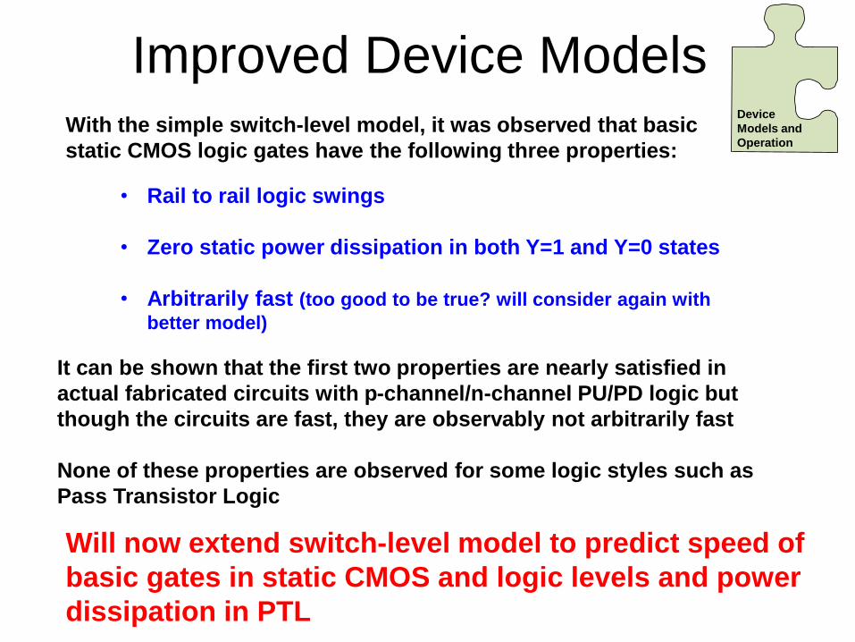
Improved Device Models
• Rail to rail logic swings
• Zero static power dissipation in both Y=1 and Y=0 states
• Arbitrarily fast (too good to be true? will consider again with
better model)
With the simple switch-level model, it was observed that basic
static CMOS logic gates have the following three properties:
It can be shown that the first two properties are nearly satisfied in
actual fabricated circuits with p-channel/n-channel PU/PD logic but
though the circuits are fast, they are observably not arbitrarily fast
None of these properties are observed for some logic styles such as
Pass Transistor Logic
Will now extend switch-level model to predict speed of
basic gates in static CMOS and logic levels and power
dissipation in PTL
Device
Models and
Operation
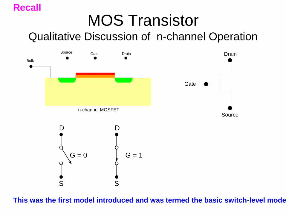
MOS TransistorQualitative Discussion of n-channel Operation
Gate DrainSource
Bulk
n-channel MOSFET
Drain
Gate
Source
Recall
D
S
G = 0
D
S
G = 1
This was the first model introduced and was termed the basic switch-level model
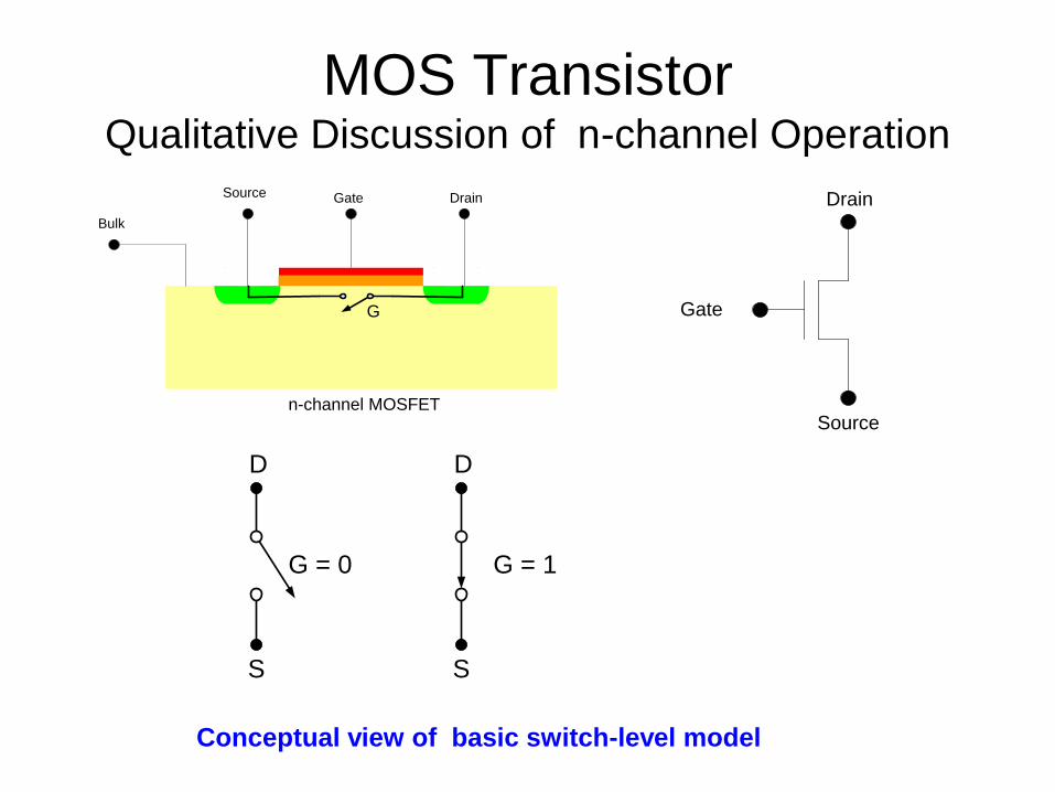
MOS TransistorQualitative Discussion of n-channel Operation
Gate DrainSource
Bulk
n-channel MOSFET
G
Drain
Gate
Source
D
S
G = 0
D
S
G = 1
Conceptual view of basic switch-level model
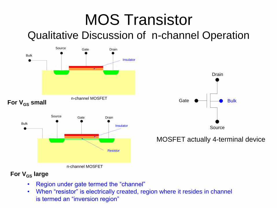
MOS TransistorQualitative Discussion of n-channel Operation
Drain
Gate
Source
Bulk
Gate DrainSource
Bulk
n-channel MOSFET
Insulator
Gate DrainSource
Bulk
n-channel MOSFET
Insulator
Resistor
For VGS small
For VGS large
• Region under gate termed the “channel”
• When “resistor” is electrically created, region where it resides in channel
is termed an “inversion region”
MOSFET actually 4-terminal device
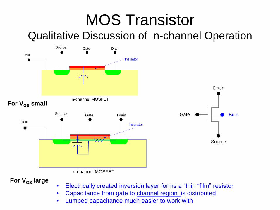
MOS TransistorQualitative Discussion of n-channel Operation
Drain
Gate
Source
Bulk
Gate DrainSource
Bulk
n-channel MOSFET
Insulator
For VGS small
For VGS large
Gate DrainSource
Bulk
n-channel MOSFET
Insulator
• Electrically created inversion layer forms a “thin “film” resistor
• Capacitance from gate to channel region is distributed
• Lumped capacitance much easier to work with
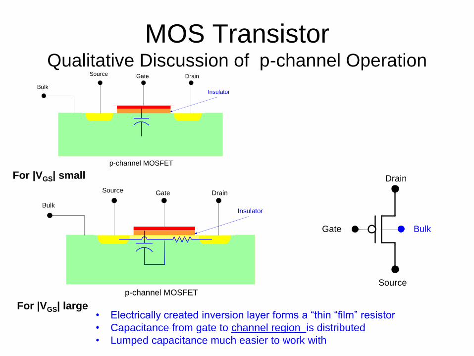
MOS TransistorQualitative Discussion of p-channel Operation
For |VGS| small
For |VGS| large• Electrically created inversion layer forms a “thin “film” resistor
• Capacitance from gate to channel region is distributed
• Lumped capacitance much easier to work with
Gate DrainSource
Bulk
p-channel MOSFET
Insulator
Gate DrainSource
Bulk
p-channel MOSFET
Insulator
Drain
Gate
Source
Bulk
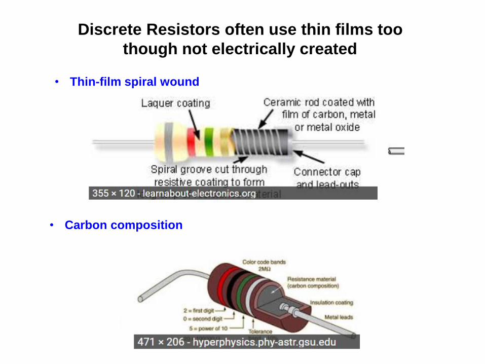
Discrete Resistors often use thin films too
though not electrically created
• Thin-film spiral wound
• Carbon composition
VG
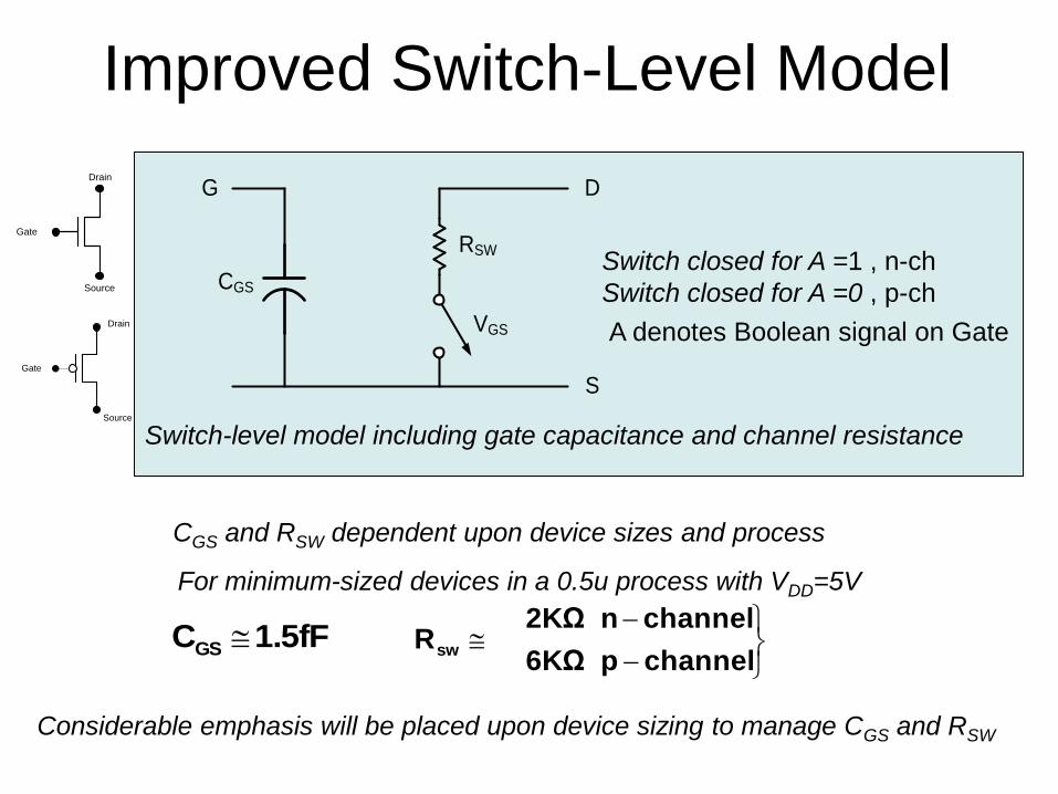
RSW
CGS
S
DG
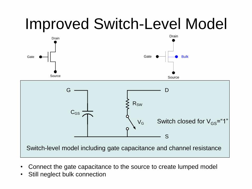
Improved Switch-Level ModelDrain
Gate
Source
Switch-level model including gate capacitance and channel resistance
Switch closed for VGS=“1”
• Connect the gate capacitance to the source to create lumped model
• Still neglect bulk connection
Drain
Gate
Source
Bulk
VGS
RSW
CGS
S
DG
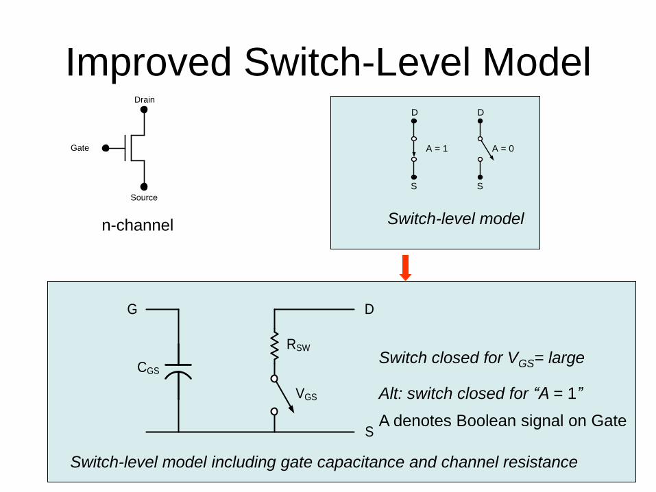
Improved Switch-Level ModelDrain
Gate
Source
D
S
A = 0
D
S
A = 1
Switch-level model
Switch-level model including gate capacitance and channel resistance
Switch closed for VGS= large
n-channel
Alt: switch closed for “A = 1”
A denotes Boolean signal on Gate
VGS
RSW
CGS
S
DG
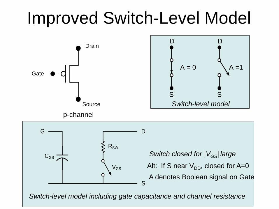
Improved Switch-Level ModelD
S
A =1
D
S
A = 0
Switch-level model
Switch-level model including gate capacitance and channel resistance
Switch closed for |VGS| large
Drain
Gate
Source
p-channel
Alt: If S near VDD, closed for A=0
A denotes Boolean signal on Gate
VGS
RSW
CGS
S
DG
Improved Switch-Level Model
Switch-level model including gate capacitance and channel resistance
Switch closed for A =1 , n-ch
Switch closed for A =0 , p-ch
CGS and RSW dependent upon device sizes and process
For minimum-sized devices in a 0.5u process with VDD=5V
1.5fFCGS
channelp6KΩ
channeln2KΩRsw
Considerable emphasis will be placed upon device sizing to manage CGS and RSW
Drain
Gate
Source
Drain
Gate
Source
A denotes Boolean signal on Gate
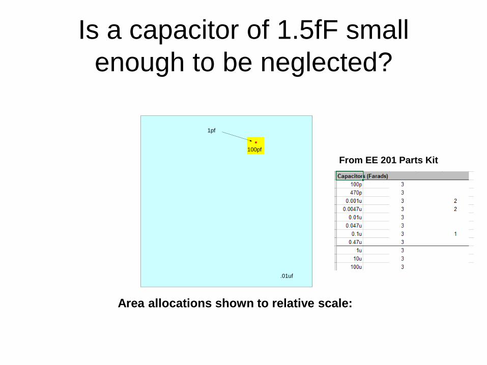
Is a capacitor of 1.5fF small
enough to be neglected?
.01uf
100pf
1pf
Area allocations shown to relative scale:
From EE 201 Parts Kit

Stay Safe and Stay Healthy !
End of Lecture 6
Related Documents