DIGITAL ELECTRONICS 03.PDF 1 E. COATES 2007 -2014 Digital Electronics 3.0 Introduction to Logic Families In this module, the differences and similarities between the various families of logic ICs available are described, along with their important operating conditions. Logic 1 and Logic 0 are a bit more complex that 5V and 0V because these digital ICs are really little analogue circuits posing as ‘Digital’. A sort of sheep in wolves clothing! Find out how logic gates actually work, and learn about the parameters that govern how the chips should be used. Special versions of the basic logic gates are also explained, such as Schmitt gates, open collectors, and buffers. The 74 series of logic ICs introduced in this module, has been the backbone of digital electronics for about the last 50 years. Although nowadays they have been replaced in many applications by bigger, faster smarter chips, the 74 series families continue to play an important role in electronics, and learning about them is a sound basis for understanding the vital basics of digital electronics. www.learnabout-electronics.org Module 3 What you´ll learn in Module 3 Section 3.0 Logic Families. • Introduction to Logic Families. Section 3.1 Power, Speed and Compatibility. • Device numbering. • Power vs. Speed • Scale of integration, SSI, MSI, VLSI. • Device compatibility. Section 3.2 How Logic gates Work. • CMOS, TTL and ECL operation. • Anti Static Protection. • Capacitance and Propagation Delay. Section 3.3 Logic IC Parameters. • Logic 1 and Logic 0. • Noise Margin. • Power Consumption. • Mixing Logic Families. • Logic Level translation. • Sinking and Sourcing. • Fan out. Section 3.4 Special Purpose Logic ICs • Open Collector Gates. • Wired Logic Functions. • Negative Logic. • Open Collector Buffers. • Schmitt Gates. Section 3.5 Logic Families Quiz. • Test your knowledge of Logic ICs.

Welcome message from author
This document is posted to help you gain knowledge. Please leave a comment to let me know what you think about it! Share it to your friends and learn new things together.
Transcript

DIGITAL ELECTRONICS 03.PDF 1 E. COATES 2007 -2014
Digital Electronics
3.0 Introduction to Logic Families
In this module, the differences and similarities between the various families of logic ICs available are described, along with their important operating conditions.
Logic 1 and Logic 0 are a bit more complex that 5V and 0V because these digital ICs are really little analogue circuits posing as ‘Digital’. A sort of sheep in wolves clothing!
Find out how logic gates actually work, and learn about the parameters that govern how the chips should be used.
Special versions of the basic logic gates are also explained, such as Schmitt gates, open collectors, and buffers.
The 74 series of logic ICs introduced in this module, has been the backbone of digital electronics for about the last 50 years. Although nowadays they have been replaced in many applications by bigger, faster smarter chips, the 74 series families continue to play an important role in electronics, and learning about them is a sound basis for understanding the vital basics of digital electronics.
www.learnabout-electronics.org
Module
3
What you´ll learn in Module 3
Section 3.0 Logic Families.
• Introduction to Logic Families.
Section 3.1 Power, Speed and Compatibility.
• Device numbering.
• Power vs. Speed
• Scale of integration, SSI, MSI, VLSI.
• Device compatibility.
Section 3.2 How Logic gates Work.
• CMOS, TTL and ECL operation.
• Anti Static Protection.
• Capacitance and Propagation Delay.
Section 3.3 Logic IC Parameters.
• Logic 1 and Logic 0.
• Noise Margin.
• Power Consumption.
• Mixing Logic Families.
• Logic Level translation.
• Sinking and Sourcing.
• Fan out.
Section 3.4 Special Purpose Logic ICs
• Open Collector Gates.
• Wired Logic Functions.
• Negative Logic.
• Open Collector Buffers.
• Schmitt Gates.
Section 3.5 Logic Families Quiz.
• Test your knowledge of Logic ICs.

www.learnabout-electronics.org Digital Electronics Module 3
DIGITAL ELECTRONICS MODULE 03.PDF 2 E. COATES 2007-2014
3.1 Logic Families Logic Families The logic gates (introduced in Module 2.1) are available in different combinations within I/C packages. As well as the basic logic functions, compatible ICs are available, which contain particular useful combinations of gates providing a convenient way of constructing more complex circuits. Hundreds of different, but directly inter-connectable logic ICs are available. The most commonly available logic ICs are the 74 series family and its sub-families, identifiable because their type numbers all start with the number 74.
74 Series Device Identification A typical 74 series IC is shown in Fig 3.1.1 and can be identified by the number MC74HC04N, which is a common structure for 74 series logic ICs, which breaks down into several sections as follows:
MC - One to three letter manufacturer’s ID code. (Motorola)
74 - Commercial grade, IC plastic package with temperature range of 0°C to +70°C although some sub families have an extended range of –40°C to +125°C.
(Also 54 Military/Aerospace grade, IC ceramic package with temperature range of –55°C to +125°C).
HC - Two to three letter code indicating sub-family (HC = High speed CMOS, HCT = High speed CMOS, TTL compatible).
04 - Two to four digit type number, indicates the type of circuit or gates with IC. 04 = Hex (6 per IC) Inverters.
N – One or two letter code for package type, e.g. N = DIP - Dual Inline Package. The codes used vary between manufacturers, but package details are usually included on the IC datasheet.
Compatibility between Logic ICs The use of a single family within a circuit design with direct connections between ICs enables circuit designers to produce circuits consisting mainly of ICs, with few extra coupling or biasing components. This greatly reduces the component count of a circuit, which among other benefits, reduces size and increases reliability.
ICs of a particular family generally use a common technology, but ICs in other families, using different technologies, usually have different input and output requirements, different supply voltages, and other parameters that affect the use of digital ICs. Making direct connections between ICs of a single family or sub family is usually very simple. ICs of different families can sometimes also be directly connected together, but may require some extra circuitry at the interface of the two IC families to maintain compatibility.
Why these different families exist dates back to the 1960s when groups of logic ICs using different technologies first became available.
Scale of Integration RTL (resistor-transistor logic) and DTL (diode-transistor logic), successfully used in early computers were superseded by TTL (transistor-transistor logic), which became the dominant
What you’ll learn in Module 3.1
After studying this section, you should be able to:
Recognise Logic Families.
• CMOS ,TTL and ECL
• Device Identification.
Understand differences between logic families.
• Speed and power considerations.
• Pin compatibility.
Fig. 3.1.1 Logic IC Device
Numbering

www.learnabout-electronics.org Digital Electronics Module 3
DIGITAL ELECTRONICS MODULE 03.PDF 3 E. COATES 2007-2014
technology. However as these ICs developed, at first as SSI (small scale integrated) devices, with just a few transistors per chip, and then as MSI (medium scale integrated) devices with 100 or more transistors, a problem arose that as more gates (and therefore more transistors) were packed into a single IC, the scale of integration would be limited by the power dissipation of the device.
Although each gate only dissipates a few milliWatts, the heat generated within a single large-scale integrated (LSI) circuit containing tens of thousands of transistors could potentially quickly destroy the IC.
It was therefore necessary to develop gates with much lower power consumption, so in the 1970s a series of CMOS (Complimentary Metal Oxide Semiconductor) ICs, called the 4000 series was developed, in which the power consumed by each gate was about 1/1000th of the power consumed by a similar TTL gate, making very large scale integration (VLSI) with millions, and more recently billions of transistors per chip possible. CMOS chips were also more flexible in their supply voltage requirements, working from supplies between 3V to 18V, compared with the TTL requirement for supplies of 5V +/- 0.25V. This made CMOS devices ideal for battery operation. However the speed at which these early CMOS devices operated was about 10 times slower than TTL.
These two logic families were not readily compatible; apart from the differences in supply voltage and speed, they were not particularly pin compatible, as illustrated in Fig. 3.1.2 so TTL chips, even simple ICs with the same types of gates as CMOS, could not be directly interchanged.
Power vs. Speed Ideally logic gates should be able to change state immediately and consume little or no power. However the laws of physics, as presently understood, say that this is not possible. All electrical circuits must consume some power, and any change in the voltages and currents in that circuit must take at least some time.
Chip designers therefore had to try and reconcile the fact that higher speeds meant more power consumption, and so some families developed, using optimum speed whilst others were developed to use the minimum of power.
CMOS (Complimentary Metal Oxide Semiconductor) chips, designed for minimum power, got faster and TTL families, using bipolar transistors for optimum speed, were developed that not only increased speed but also reduced power consumption.
As the overall performance of these families increased they also became more compatible. The increase in portable (battery powered) electronic devices along with the ability of chip manufacturers to make the component parts of ICs much smaller also meant that power could be reduced and speed
Fig. 3.1.2 Original CMOS and
TTL Pinouts for Comparable
NAND gate ICs
Fig 3.1.3 Logic Families Power vs Speed
www.learnabout-electronics.org Digital Electronics Module 3
DIGITAL ELECTRONICS MODULE 03.PDF 4 E. COATES 2007-2014
increased.
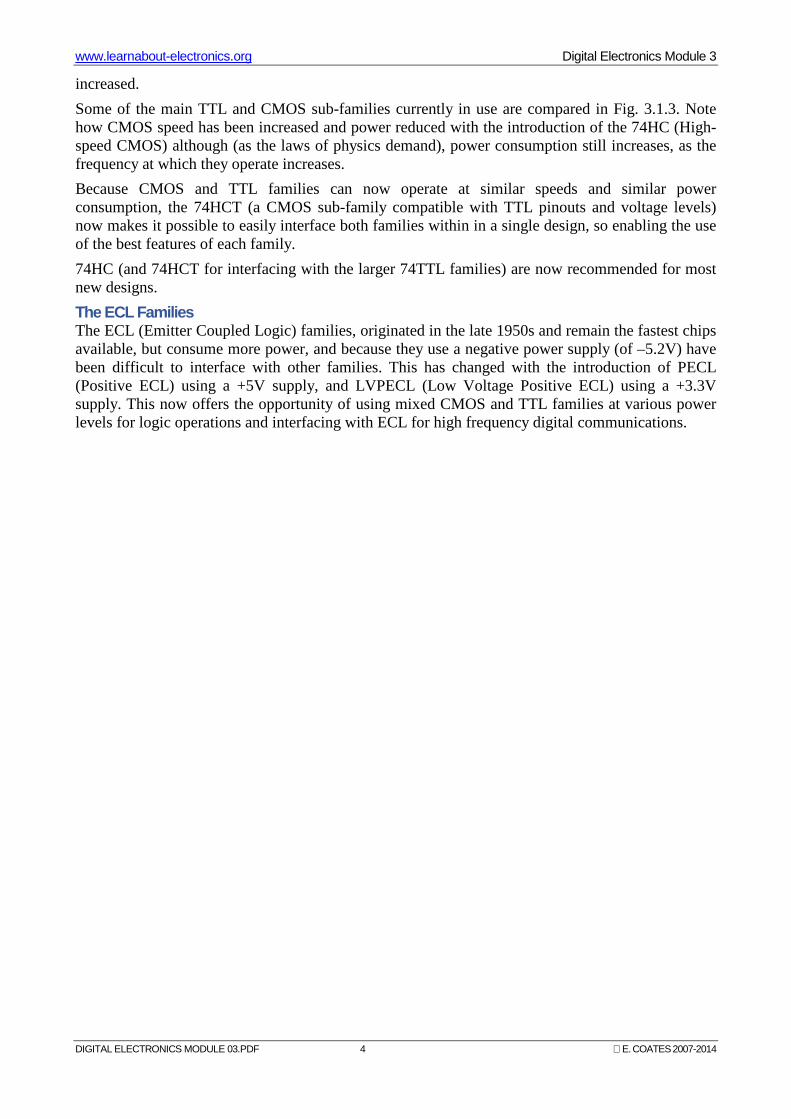
Some of the main TTL and CMOS sub-families currently in use are compared in Fig. 3.1.3. Note how CMOS speed has been increased and power reduced with the introduction of the 74HC (High-speed CMOS) although (as the laws of physics demand), power consumption still increases, as the frequency at which they operate increases.
Because CMOS and TTL families can now operate at similar speeds and similar power consumption, the 74HCT (a CMOS sub-family compatible with TTL pinouts and voltage levels) now makes it possible to easily interface both families within in a single design, so enabling the use of the best features of each family.
74HC (and 74HCT for interfacing with the larger 74TTL families) are now recommended for most new designs.
The ECL Families The ECL (Emitter Coupled Logic) families, originated in the late 1950s and remain the fastest chips available, but consume more power, and because they use a negative power supply (of –5.2V) have been difficult to interface with other families. This has changed with the introduction of PECL (Positive ECL) using a +5V supply, and LVPECL (Low Voltage Positive ECL) using a +3.3V supply. This now offers the opportunity of using mixed CMOS and TTL families at various power levels for logic operations and interfacing with ECL for high frequency digital communications.

www.learnabout-electronics.org Digital Electronics Module 3
DIGITAL ELECTRONICS MODULE 03.PDF 5 E. COATES 2007-2014
3.2 How Logic Gates Work Logic Technologies Small and medium scale (SSI and MSI) Logic IC families are currently made in a wide range of sub-families and a variety of package types, using three basically different technologies:
• TTL (Transistor Transistor Logic)
• CMOS (Complimentary Metal Oxide Semiconductor)
• ECL (Emitter Coupled Logic)
TTL TTL gates use a 5V (±0.25V) supply, and are capable of high-speed operation. Over 600 different logic ICs are available, covering a very wide range of digital functions. Due to the use of bipolar transistors, TTL has much higher power consumption than similar CMOS types, when working at relatively low frequencies. As the frequency of signals handled increases however, this difference decreases as the power consumption of CMOS increases and TTL power consumption remains nearly constant.
Operation Notice that this circuit looks similar to those found in analogue push pull amplifiers, except that the transistors here are driven either into cut-off or saturation, rather than working in their linear operating condition. Also, being constructed within an IC, it can use a device not normally found in conventional analogue amplifiers, a multi emitter transistor.
Fig. 3.2.2 shows a typical schematic for a TTL NAND gate. R1 is a low value resistor (about 4K) and as the base current of T1 is small, the base voltage is about +5V. If both emitters of T1 are at logic 1, (also around +5V), there will be very little potential difference between base and emitter, and T1 will be turned off. As T1 is not conducting, its collector will also be at about 5V, and due to this high potential, T2 base will have a higher potential than its emitter, which will cause T2 to conduct heavily and go into saturation.
T2 collector will therefore fall to a low potential, and the emitter voltage of T2 will rise due to the current flow through R3. The voltage across R3 will rise to a sufficient level (about 0.7V) to fully turn on T3. As T3 saturates, its collector voltage will fall to about 0.2V, thus giving a logic 0 state at the output terminal.
T4 emitter voltage is made up of T3 VCE (about 0.2V) plus the forward voltage drop across D1, which will be about 0.7V, giving an emitter potential of 0.2V + 0.7V = 0.9V, the same as its base voltage.
What you’ll learn in Module 3.2
After studying this section you should be able to:
Understand How Logic gates Work.
• CMOS, TTL and ECL.
• Supply voltages.
• Propagation delay.
Fig. 3.2.2 Schematic diagram
of a TTL NAND Gate
Fig 3.2.1 Typical Logic IC
Packages
www.learnabout-electronics.org Digital Electronics Module 3
DIGITAL ELECTRONICS MODULE 03.PDF 6 E. COATES 2007-2014
The base potential of T4 is made up of T3 base/emitter potential VBE (about 0.7V), plus the collector/emitter, potential (VCE) of T2, (about 0.2V), giving a base voltage for T4 of about 0.9V. Therefore the base and emitter voltages on T4 are approximately equal, so T4 will be turned off.
With BOTH input terminals at logic 1 therefore, the output terminal will be at logic 0, the correct operation for a NAND gate.
If either one of the inputs is taken to logic 0 however, this will make T1 conduct, as the emitter that is at logic 0 will be at a lower voltage than that supplied to the base by R1. This will cause T1 to saturate, taking its collector to a low potential (less than 0.8V) and as this is also connected to T2 base T2 will turn off, making its collector voltage and T4 base voltage, rise to very nearly +Vcc.
As virtually no current (ICE) is flowing through T2 collector/emitter circuit, practically no voltage is developed across the emitter resistor R3, reducing T3 base voltage to 0V, and so T3 is turned off. However, sufficient current will be flowing out of the output terminal (feeding the next gate input circuit) to cause T4 emitter to be held at about 4.1V. This is 0.9V below +Vcc, made up of the voltage across D1 (0.7V) plus the saturation voltage VCE of T4 (0.2V). This places about 4V or logic 1 (between 2.4V and 5V) on the output terminal.
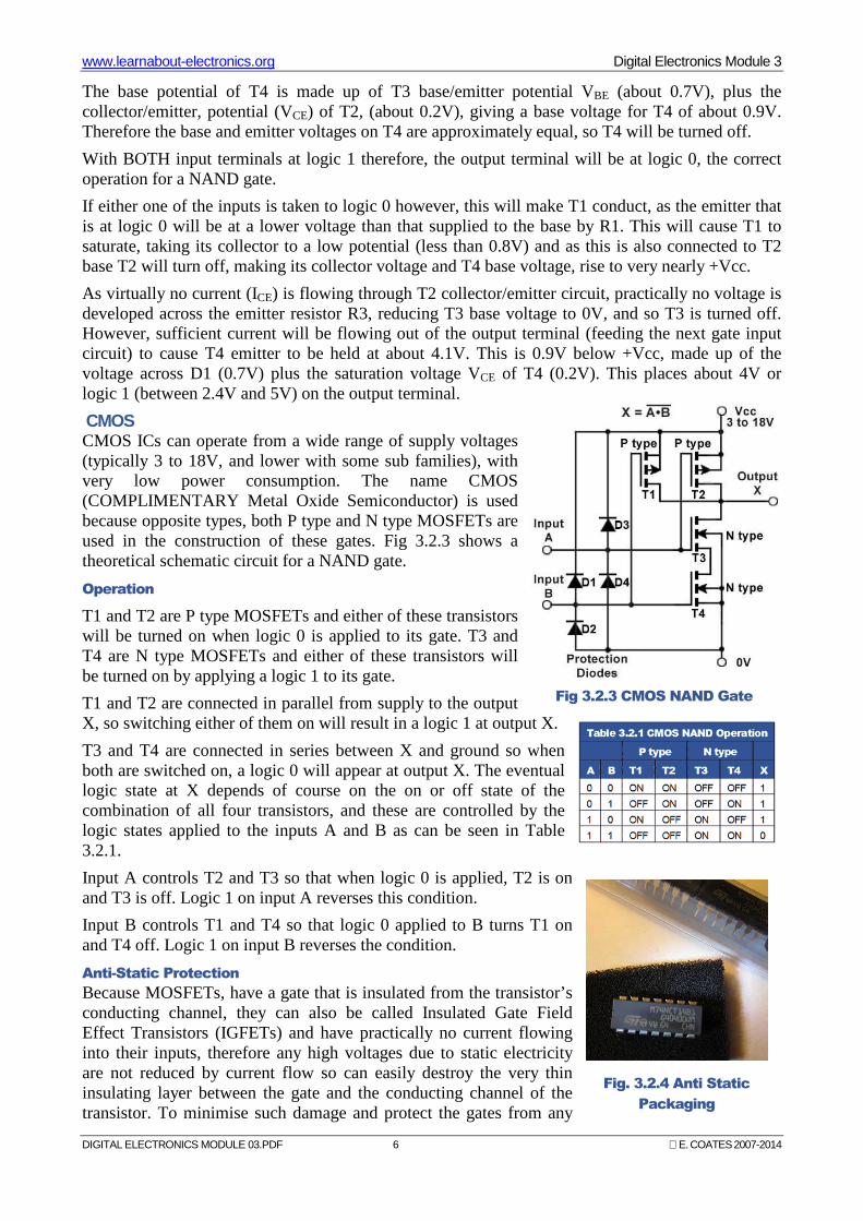
CMOS CMOS ICs can operate from a wide range of supply voltages (typically 3 to 18V, and lower with some sub families), with very low power consumption. The name CMOS (COMPLIMENTARY Metal Oxide Semiconductor) is used because opposite types, both P type and N type MOSFETs are used in the construction of these gates. Fig 3.2.3 shows a theoretical schematic circuit for a NAND gate.
Operation
T1 and T2 are P type MOSFETs and either of these transistors will be turned on when logic 0 is applied to its gate. T3 and T4 are N type MOSFETs and either of these transistors will be turned on by applying a logic 1 to its gate.
T1 and T2 are connected in parallel from supply to the output X, so switching either of them on will result in a logic 1 at output X.
T3 and T4 are connected in series between X and ground so when both are switched on, a logic 0 will appear at output X. The eventual logic state at X depends of course on the on or off state of the combination of all four transistors, and these are controlled by the logic states applied to the inputs A and B as can be seen in Table 3.2.1.
Input A controls T2 and T3 so that when logic 0 is applied, T2 is on and T3 is off. Logic 1 on input A reverses this condition.
Input B controls T1 and T4 so that logic 0 applied to B turns T1 on and T4 off. Logic 1 on input B reverses the condition.
Anti-Static Protection
Because MOSFETs, have a gate that is insulated from the transistor’s conducting channel, they can also be called Insulated Gate Field Effect Transistors (IGFETs) and have practically no current flowing into their inputs, therefore any high voltages due to static electricity are not reduced by current flow so can easily destroy the very thin insulating layer between the gate and the conducting channel of the transistor. To minimise such damage and protect the gates from any
Fig. 3.2.4 Anti Static
Packaging
Fig 3.2.3 CMOS NAND Gate

www.learnabout-electronics.org Digital Electronics Module 3
DIGITAL ELECTRONICS MODULE 03.PDF 7 E. COATES 2007-2014
high voltage static electricity spikes that may appear across the IC during handling, CMOS ICs should always be stored in anti static packaging, and handled in accordance with manufacturers handling procedures.
To protect the ICs from high voltage spikes when in circuit, protection diodes (see Fig. 3.2.3) are used at the gate inputs.
Protection diode D3 is connected between input A and +Vcc so that if any voltage higher than Vcc appears at input A, D3 will become forward biased and conduct, limiting the input voltage to +Vcc.
Similarly, if a negative voltage appears at input A, D4 will conduct, limiting the input voltage to no less than 0V.
Input B is protected in a similar manner by D1 and D2. Note however, that although the diodes offer protection, it is still possible that very large static voltages may still damage these devices, so anti-static precautions should always be used when handling CMOS devices.
Capacitance in CMOS devices
Because CMOS transistors are IGFETs with insulating layers between electrodes, they naturally act as capacitors. The value of these capacitors is of course small because the electrodes either side of the very thin insulating layer are extremely small. However the combined capacitance between the various sections of the several IGFETs that make up a CMOS gate, added to any capacitance between lead-out wires etc. is sufficient to have an effect on the overall gate performance. When a change in logic state occurs, ideally it should complete its transition from 0 to 1, or 1 to 0 immediately. However because of the gate capacitance and internal resistances that are present, the change cannot happen in less time than the CR time constant of the circuit. The output of a gate cannot complete its change until the input has completed its transition, and the output must similarly take some additional time, before reaching its new value.
Propagation Delay
Any gate introduces some delay between when its input changes and when a resulting change takes place at its output. This is called the propagation delay of the gate, and is made up of two, often different delays, as shown in Fig. 3.2.5 using a simple inverter gate as an example.
The High to Low Propagation Time (tPHL) measured from the time (usually in nanoseconds) when the input rises past the 50% level to the time when the output falls past the 50% level. A similar, but usually longer delay (tPLH) is measured from when the input falls past the 50% level to when the output rises past the 50% level. Therefore the average propagation delay of the gate is:
(tPHL + tPLH) / 2
Typical average propagation delay for a 74HC04 inverter is about 8ns.
Fig. 3.2.5 Propagation Delay

www.learnabout-electronics.org Digital Electronics Module 3
DIGITAL ELECTRONICS MODULE 03.PDF 8 E. COATES 2007-2014
ECL Because the early designs of ECL ICs needed a negative supply voltage of -5.2V they were not particularly compatible with either CMOS or TTL circuits, even though, like TTL, they use bipolar transistors. However there are now newer ECL sub families available that use positive supplies such as PECL (+5V) and LVPECL (+3.3V). Although the supply voltages for these ECL gates are now more compatible with CMOS and TTL, the logic levels used in ECL are quite different to other logic families. ECL is extremely fast in operation with propagation delays of less than 1 nanosecond available.
ECL was extensively used in early super computers, but because of its high power requirement (up to 40mW per gate) fell out of general use. Today modern ECL sub families such as PECL or LVPECL are now mainly used for interfacing CMOS or TTL digital systems to high frequency signal communication (up to several GHz) circuits. The two opposite logic state outputs
(VOUT and VOUT ) means that the ECL OR gate illustrated in Fig. 3.2.6 can operate as an OR gate or
a NOR gate and also makes ECL for interfacing with differential (two conductor) transmission lines possible. This method of transferring high-speed digital data uses a pair of high frequency anti-phase signals as a method of cancelling out electromagnetic interference that may be picked up during transmission
Operation
The basis of the ECL circuit is a differential amplifier (T3 and T4 in Fig. 3.2.6), which is ideal for high frequency use and reducing noise on the amplified signals. This amplifier compares the voltage at the inputs (the bases of T1 and T3) with a steady reference voltage produced by T5, D1 and D2. To avoid any delay caused by the transistors saturating, the differential amplifier is designed to always be in a linear amplifying mode, approximately half way between saturation and cut off.
The voltage change between logic 1 and logic 0 is between –0.9 and –1.75 respectively. Power consumption is considerably higher than CMOS or TTL because the transistors in the differential amplifier are always conducting, rather than switching on and off as in TTL and CMOS.
ECL and PECL use differential transmission, a pair of conductors with opposite polarity signals, along which data can be transmitted for around 50m. The technique reduces interference in the transmission lines when passing data from one digital system to another, and was used in many data transmission links in computing up to the 1990s, but for many uses, such as USB, HDMI etc. ECL has now been largely superseded by LVDS (Low Voltage Differential Signalling), a CMOS based high frequency digital transmission system. This system uses much less power than ECL and can transfer data over distances of up to 10m at a rate of several hundred Megabits per second.
Fig 3.2.6 ECL OR/NOR Gate

www.learnabout-electronics.org Digital Electronics Module 3
DIGITAL ELECTRONICS MODULE 03.PDF 9 E. COATES 2007-2014
3.3 Logic IC Parameters Logic 1 and Logic 0
Logic 1 and Logic 0 are not simply 5V and 0V or even Vcc and Ground. Within any family of ICs the voltages and currents indicating 1 and 0 cover defined ranges unique to that logic family. The range of voltages allowed for a particular logic level depends on the amount of current flowing into or out of the logic gate inputs or output, the larger the current the output is supplying, the lower the output voltage will be.
Each output will supply a certain amount of current before the output voltage falls too far to be called logic 1, and each gate input will need to be supplied with a certain amount of current to raise the input voltage sufficiently to be recognised as logic 1.
Examples of typical logic levels at inputs and outputs in a range of logic families are illustrated in Fig. 3.3.1. These levels are fairly standard throughout a particular family, although there can be minor differences in these and other parameters, between products from different manufacturers. In addition there are sub families within these families that may have different defined levels. When designing digital circuits, or replacing ICs in critical equipment, it is therefore essential to consult the appropriate manufacturer’s data sheets.
Logic 1 levels for inputs and outputs are shown in red and logic 0 in green. To highlight the fact that true ECL gates, have negative logic levels, these colours have been changed to yellow and blue respectively.
Notice that the logic levels for outputs (left column) and inputs (right column) in all of the families are different. This ensures that provided that the output voltage of a gate is within its defined logic limits for 1 or 0, any compatible gate input connected to that output will recognise the correct 1 or 0 levels. The difference between levels at the output and input in any particular family is called the ‘Noise Margin’.
What you’ll learn in Module 3.3
After studying this section, you should be able to:
Define 1 and 0 logic levels used in common logic families.
• LSTTL
• HC/HCT
• ECL/ PECL
Understand common terms relation to logic gates.
• Noise Margin.
• Sinking and Sourcing.
• Fan out (AC and DC).
• Minimising Power Consumption.
• Mixing Logic Families.
• Logic Level Translation.
Fig. 3.3.1 Logic Levels

www.learnabout-electronics.org Digital Electronics Module 3
DIGITAL ELECTRONICS MODULE 03.PDF 10 E. COATES 2007-2014
Noise Margin Because voltages in digital circuits can be continually changing very rapidly between logic 1 and logic 0, (virtually between supply voltage and ground), they have the potential to produce a lot of noise, in the form of high frequency voltage spikes on the IC power supply lines.
To counteract this it is important to include effective decoupling, not only at the power supply unit, but also by connecting decoupling capacitors across the VDD and 0V connections at each IC. These capacitors are normally connected as physically close to the IC as possible, as shown in Fig. 3.3.2.
Despite these measures, it is possible that some noise will remain that could disturb the logic levels of digital signals. However logic ICs have a built in ‘Noise Margin’, illustrated in Fig. 3.3.3. This is the difference between the worst-case voltage (VOH) for logic 1 at the output, which is 2.4V in the case of 74HCT, and the minimum voltage required for logic 1 to be recognised at the input (VIH), 2.0V in 74HCT. This difference (0.4V) should be enough to ensure that noise does not cause a wrong logic level to be seen by the 74HCT input; a similar noise margin is provided for logic 0 (VIL-VOL) as shown in Fig. 3.3.3.
It can be seen from Fig. 3.3.1 that different logic families have very different noise margins. The CMOS 74HC gates have a much wider noise margin than LS TTL or the TTL compatible 74HCT series, making them much more tolerant of noise. This is because the CMOS outputs are normally driven very close to VDD or 0V as very little current is drawn from a CMOS output to drive any CMOS inputs connected to it.
Minimising Power Consumption
In both CMOS and TTL ranges it is important that the central (white) range of voltages in Fig. 3.3.1 is avoided as much as possible. This is done by ensuring that switching between 1 and 0 is as fast as possible. If the IC is operating within the ‘invalid range’, power consumption increases dramatically. When the output voltage is close to the supply voltage, current is almost zero and therefore power (V x I) is very low. Similarly when the output is close to 0V but maximum current is flowing, V x I is again very low. Power consumption is at its highest when both voltage and current are around the mid range, and operating the ICs in this range would substantially increase the heat dissipated by the IC.
However, any unused inputs on CMOS ICs will tend to float to a mid voltage level, causing power dissipation to increase. To avoid problems with floating CMOS inputs, they should therefore be connected to either supply or ground, either directly or via a resistor, so they are not allowed to ‘float’ and cause excessive power consumption. This is not absolutely necessary, (though good practice), with TTL ICs as any unused TTL inputs will float up to logic 1.
Notice that ECL/PECL gates operate exclusively in this mid range area; this is why power consumption in these families is higher than in TTL or CMOS. However the close proximity of the logic 1 and logic 0 values in ECL allows for much higher switching speeds. This operation also gives ECL a much narrower noise margin however, making these chips more susceptible to noise. This was the reason for the original ECL family having its positive supply tied to 0V, which is generally less noisy than sharing a positive supply with many other ICs.
Fig. 3.3.2 Logic IC Decoupling
Fig. 3.3.3 Noise Margin
www.learnabout-electronics.org Digital Electronics Module 3
DIGITAL ELECTRONICS MODULE 03.PDF 11 E. COATES 2007-2014
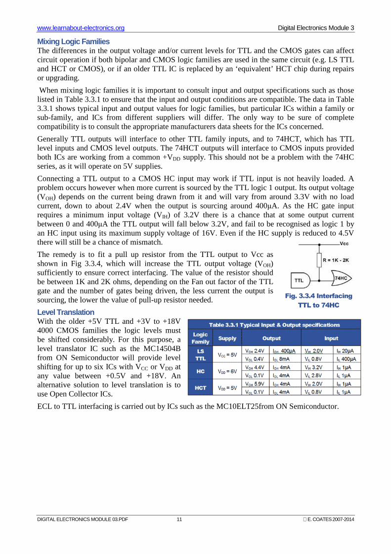
Mixing Logic Families The differences in the output voltage and/or current levels for TTL and the CMOS gates can affect circuit operation if both bipolar and CMOS logic families are used in the same circuit (e.g. LS TTL and HCT or CMOS), or if an older TTL IC is replaced by an ‘equivalent’ HCT chip during repairs or upgrading.
When mixing logic families it is important to consult input and output specifications such as those listed in Table 3.3.1 to ensure that the input and output conditions are compatible. The data in Table 3.3.1 shows typical input and output values for logic families, but particular ICs within a family or sub-family, and ICs from different suppliers will differ. The only way to be sure of complete compatibility is to consult the appropriate manufacturers data sheets for the ICs concerned.
Generally TTL outputs will interface to other TTL family inputs, and to 74HCT, which has TTL level inputs and CMOS level outputs. The 74HCT outputs will interface to CMOS inputs provided both ICs are working from a common +VDD supply. This should not be a problem with the 74HC series, as it will operate on 5V supplies.
Connecting a TTL output to a CMOS HC input may work if TTL input is not heavily loaded. A problem occurs however when more current is sourced by the TTL logic 1 output. Its output voltage (VOH) depends on the current being drawn from it and will vary from around 3.3V with no load current, down to about 2.4V when the output is sourcing around 400µA. As the HC gate input requires a minimum input voltage (VIH) of 3.2V there is a chance that at some output current between 0 and 400µA the TTL output will fall below 3.2V, and fail to be recognised as logic 1 by an HC input using its maximum supply voltage of 16V. Even if the HC supply is reduced to 4.5V there will still be a chance of mismatch.
The remedy is to fit a pull up resistor from the TTL output to Vcc as shown in Fig 3.3.4, which will increase the TTL output voltage (VOH) sufficiently to ensure correct interfacing. The value of the resistor should be between 1K and 2K ohms, depending on the Fan out factor of the TTL gate and the number of gates being driven, the less current the output is sourcing, the lower the value of pull-up resistor needed.
Level Translation With the older +5V TTL and +3V to +18V 4000 CMOS families the logic levels must be shifted considerably. For this purpose, a level translator IC such as the MC14504B from ON Semiconductor will provide level shifting for up to six ICs with VCC or VDD at any value between +0.5V and +18V. An alternative solution to level translation is to use Open Collector ICs.
ECL to TTL interfacing is carried out by ICs such as the MC10ELT25from ON Semiconductor.
Fig. 3.3.4 Interfacing
TTL to 74HC
www.learnabout-electronics.org Digital Electronics Module 3
DIGITAL ELECTRONICS MODULE 03.PDF 12 E. COATES 2007-2014
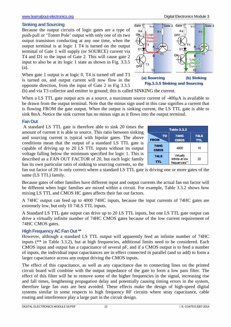
Sinking and Sourcing Because the output circuits of logic gates are a type of push-pull or ‘Totem Pole’ output with only one of its two output transistors conducting at any one time, when the output terminal is at logic 1 T4 is turned on the output terminal of Gate 1 will supply (or SOURCE) current via T4 and D1 to the input of Gate 2. This will cause gate 2 input to also be at its logic 1 state as shown in Fig. 3.3.5 (a).
When gate 1 output is at logic 0, T4 is turned off and T3 is turned on, and output current will now flow in the opposite direction, from the input of Gate 2 in Fig 3.3.5 (b) and via T3 collector and emitter to ground; this is called SINKING the current.
When a LS TTL gate output acts as a source, a maximum source current of -400µA is available to be drawn from the output terminal. Note that the minus sign used in this case signifies a current that is flowing FROM the gate output. When the output is sinking current, the LS TTL gate is able to sink 8mA. Notice the sink current has no minus sign as it flows into the output terminal.
Fan Out A standard LS TTL gate is therefore able to sink 20 times the amount of current it is able to source. This ratio between sinking and sourcing current is typical with bipolar gates. The above conditions mean that the output of a standard LS TTL gate is capable of driving up to 20 LS TTL inputs without its output voltage falling below the minimum specified for logic 1. This is described as a FAN OUT FACTOR of 20, but each logic family has its own particular ratio of sinking to sourcing currents, so the fan out factor of 20 is only correct where a standard LS TTL gate is driving one or more gates of the same (LS TTL) family.
Because gates of other families have different input and output currents the actual fan out factor will be different when logic families are mixed within a circuit. For example, Table 3.3.2 shows how mixing LS TTL and CMOS HC gates affects their fan out factors.
A 74HC output can feed up to 4000 74HC inputs, because the input currents of 74HC gates are extremely low, but only 10 74LS TTL inputs.
A Standard LS TTL gate output can drive up to 20 LS TTL inputs, but one LS TTL gate output can drive a virtually infinite number of 74HC CMOS gates because of the low current requirement of 74HC CMOS gates.
High Frequency AC Fan Out ** However, although a standard LS TTL output will apparently feed an infinite number of 74HC inputs (** in Table 3.3.2), but at high frequencies, additional limits need to be considered. Each CMOS input and output has a capacitance of several pF, and if a CMOS output is to feed a number of inputs, the individual input capacitances are in effect connected in parallel (and so add) to form a larger capacitance across any output driving the CMOS inputs.
The effect of this capacitance, as well as any capacitance due to connecting lines on the printed circuit board will combine with the output impedance of the gate to form a low pass filter. The effect of this filter will be to remove some of the higher frequencies in the signal, increasing rise and fall times, lengthening propagation delay and potentially causing timing errors in the system, therefore large fan outs are best avoided. These effects make the design of high-speed digital systems similar in some respects to high frequency RF circuits where stray capacitance, cable routing and interference play a large part in the circuit design.
(a) Sourcing (b) Sinking
Fig.3.3.5 Sinking and Sourcing

www.learnabout-electronics.org Digital Electronics Module 3
DIGITAL ELECTRONICS MODULE 03.PDF 13 E. COATES 2007-2014
3.4 Special Purpose Logic ICs
Open Collector Gates Fig. 3.4.1 shows the internal circuit of an open collector NAND gate. The grey area illustrates a single gate within an IC. Instead of the normal Totem Pole output stage, the single output transistor T3 has its collector brought out to an external pin, which can be connected to an external power supply, at a different voltage to the VCC supply of the IC, via an external load resistor REXT.
In Fig. 3.4.1, when both inputs A and B are at logic 0, the high voltage applied to T1 base will cause it to turn on, so that T1 collector will go to near 0V and T2 will turn off.
As T2 is off there will be virtually no current through R3 so the voltage at T3 gate will be around 0V. T3 will therefore be turned off and the external pull up resistor REXT will pull the collector voltage of T3 up to +V, which will be at the valid logic 1 level of the next gate.
Logic Level Translation
Open collector and open drain gates can therefore be used for changing the levels of an output to match the higher or lower logic levels of an input on a different family of gates, when gates of mixed families are used.
Open collector gates can be used with external collector VCC supplies having a voltage typically somewhere between +1.5V to +5.5V for logic gates, Buffer ICs are also available that can operate on collector VCC supplies up to +30V. The maximum value of collector voltage is set by the VOH parameter of the open collector gate.
Wired Logic Functions Open collector ICs are available in most of the logic types, AND, NAND etc, with the exception of OR gates. However open collector gates can be used to make both wired AND and wired OR functions as shown in Figs. 3.4.2 and 3.4.3. The outputs of gates without open collectors must not be connected together, because if the outputs happen to be at opposite logic states, the gate with a logic 0 output will try to sink more current than the logic 1 gate can source, and damage will most probably occur. However with open collector (or drain) gates, a gate output at logic 0 will be sinking current drawn from the external pull up resistor REXT, and any other connected open collector gate trying to output a logic 1 will have its output transistor turned off and so will not be sourcing any current.
Fig. 3.4.1 Simplified circuit of
an Open Collector NAND Gate
What you’ll learn in Module 3.4
After studying this section, you should be able to:
Understand the need for Special Purpose Logic ICs.
• Open Collector Gates.
• Wired Logic Functions.
• Negative Logic.
• Buffers.
• Schmitt Gates.

www.learnabout-electronics.org Digital Electronics Module 3
DIGITAL ELECTRONICS MODULE 03.PDF 14 E. COATES 2007-2014
Wired AND
If two or more open collector gate outputs are connected together, any gate with a logic 0 output will pull all other connected outputs to logic 0, giving an output of logic 0 at output X, but if all the connected outputs are at logic 1, then X will be at logic 1, the action of an ‘invisible’ AND gate.
Wired OR
It is also possible to implement a wired OR function using open collector (or drain) gates as shown in Fig. 3.4.3, although the explanation here is a little more complex as it involves using Negative Logic.
The circuit in Fig. 3.4.3 is used to obtain the Boolean function (A•B)+(C•D) without using a physical OR gate.
Notice that the circuit in Fig. 3.4.3 is similar to the wired AND circuit in Fig. 3.4.2, except that the two open collector AND gates have been replaced by two open collector NAND gates.
The main difference with this circuit however is that to obtain an OR function from what appears to be a wired AND function, Negative Logic is applied.
Negative Logic In Digital Electronics it is usual to explain the operation of a circuit theoretically in terms of 1 and 0, but the actual gates are really just specialised analogue circuits. As explained in Module 3.3, the outputs normally thought of as 1s and 0s are really ranges of voltage and current, 1 and 0 are no more than convenient names given to these voltages and currents. It is also usually assumed that logic 1 refers to the higher of the two voltage ranges – but that need not be so! Also logic 1 is normally the active state of an output, and logic 0 is the inactive state, but this is not always what is required.
For example, the source current available from an open collector gate output when it is at logic 1 is very small, compared to the current the gate will sink when its output transistor is turned on, giving an output of logic 0.
It is quite reasonable therefore, to drive some output device, such as a lamp or relay for example, using the higher current available from a logic 0 output, as shown in Fig. 3.4.4.
In negative logic it is assumed that the active state is the low voltage state and that this is called logic 1. What this does to the familiar truth tables used in positive logic is to replace all the logic 1s (previously assumed to be the active state) with logic 0s and vice versa.
The effect of this reversal of logic states can be seen in Table 3.4.1. The X column for the positive AND gate is as would be expected; a logic 1 when both A and B are 1, otherwise logic 0s. However using negative logic on the same physical AND gate, simply swapping the 1s and 0s in both the input and output columns has changed the X output column from three 0s and a 1, to three 1s and a 0, so that X = 1 whenever A or B is 1. The AND gate has been transformed to an OR gate!
Fig 3.4.2 Wired AND Function
Fig 3.4.4 Active Zero
Fig. 3.4.3 Wired OR Function
www.learnabout-electronics.org Digital Electronics Module 3
DIGITAL ELECTRONICS MODULE 03.PDF 15 E. COATES 2007-2014
Using negative logic will change the function of any of the six two input logic gates, if you want to see what happens, try re-writing the truth tables for AND, OR, NAND, NOR, XOR, and XNOR in a similar manner to Table 3.4.1. However, negative logic is not widely used and so unless a logic circuit is actually described as using negative logic, it can be assumed that positive logic is being applied.
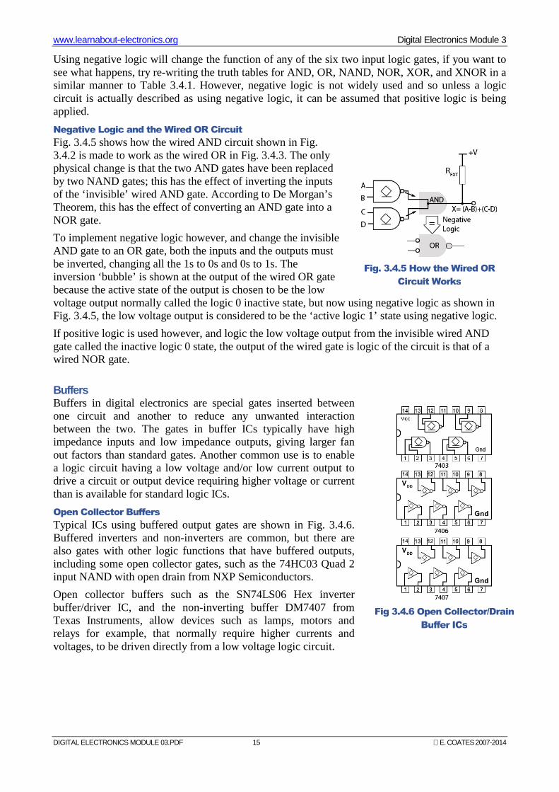
Negative Logic and the Wired OR Circuit
Fig. 3.4.5 shows how the wired AND circuit shown in Fig. 3.4.2 is made to work as the wired OR in Fig. 3.4.3. The only physical change is that the two AND gates have been replaced by two NAND gates; this has the effect of inverting the inputs of the ‘invisible’ wired AND gate. According to De Morgan’s Theorem, this has the effect of converting an AND gate into a NOR gate.
To implement negative logic however, and change the invisible AND gate to an OR gate, both the inputs and the outputs must be inverted, changing all the 1s to 0s and 0s to 1s. The inversion ‘bubble’ is shown at the output of the wired OR gate because the active state of the output is chosen to be the low voltage output normally called the logic 0 inactive state, but now using negative logic as shown in Fig. 3.4.5, the low voltage output is considered to be the ‘active logic 1’ state using negative logic.
If positive logic is used however, and logic the low voltage output from the invisible wired AND gate called the inactive logic 0 state, the output of the wired gate is logic of the circuit is that of a wired NOR gate.
Buffers Buffers in digital electronics are special gates inserted between one circuit and another to reduce any unwanted interaction between the two. The gates in buffer ICs typically have high impedance inputs and low impedance outputs, giving larger fan out factors than standard gates. Another common use is to enable a logic circuit having a low voltage and/or low current output to drive a circuit or output device requiring higher voltage or current than is available for standard logic ICs.
Open Collector Buffers
Typical ICs using buffered output gates are shown in Fig. 3.4.6. Buffered inverters and non-inverters are common, but there are also gates with other logic functions that have buffered outputs, including some open collector gates, such as the 74HC03 Quad 2 input NAND with open drain from NXP Semiconductors.
Open collector buffers such as the SN74LS06 Hex inverter buffer/driver IC, and the non-inverting buffer DM7407 from Texas Instruments, allow devices such as lamps, motors and relays for example, that normally require higher currents and voltages, to be driven directly from a low voltage logic circuit.
Fig. 3.4.5 How the Wired OR
Circuit Works
Fig 3.4.6 Open Collector/Drain
Buffer ICs
www.learnabout-electronics.org Digital Electronics Module 3
DIGITAL ELECTRONICS MODULE 03.PDF 16 E. COATES 2007-2014
Schmitt Gates The digital signals processed by logic gates need to have fast rising and falling edges. Taking too much time to change logic states, spending too long in the ‘invalid’ zone between states, can cause unreliable logic levels, timing problems and excessive power dissipation, even shortening the life of logic ICs. Standard gate inputs change from 0 to 1 or 1 to 0 at a voltage of about 2.0V. If there is any noise on the input signal, it may be rapidly changing its voltage above and below this level, so causing the gate to rapidly change state if the noise exceeds the noise margin. These rapid and uncertain changes in the gate’s input circuit will also cause the output to oscillate between 1 and 0, transmitting the problem to any subsequent gates in the digital system.
To avoid these problems, gates with Schmitt inputs such as those shown in Fig. 3.4.7 are often used, especially at the input to a system where noise may be expected, as signals arrive from an external source.
Schmitt gates use positive feedback, which causes the gate to switch between logic states extremely quickly. They also have a hysteresis effect, which only allows a change of state to occur as the input voltage passes two specific and different voltages, the Positive-going input threshold voltage (VT+) and the Negative-going input threshold voltage (VT-).
As the input voltage passes VT+ during a positive going transition, the gate input changes very rapidly to its high state. It then cannot return to its low state until the input voltage falls to the lower level of VT-.
This action has several beneficial effects on poor input signals, as illustrated in Fig. 3.4.8.
(a) It can be used to change slowly changing signals to square waves having very fast transitions.
(b) Noise can be removed from signals, provided that the amplitude of the noise is not greater than ∆VT.
(c) Slow rise and fall times can be restored to practically instant transitions by feeding the signal through a Schmitt trigger.
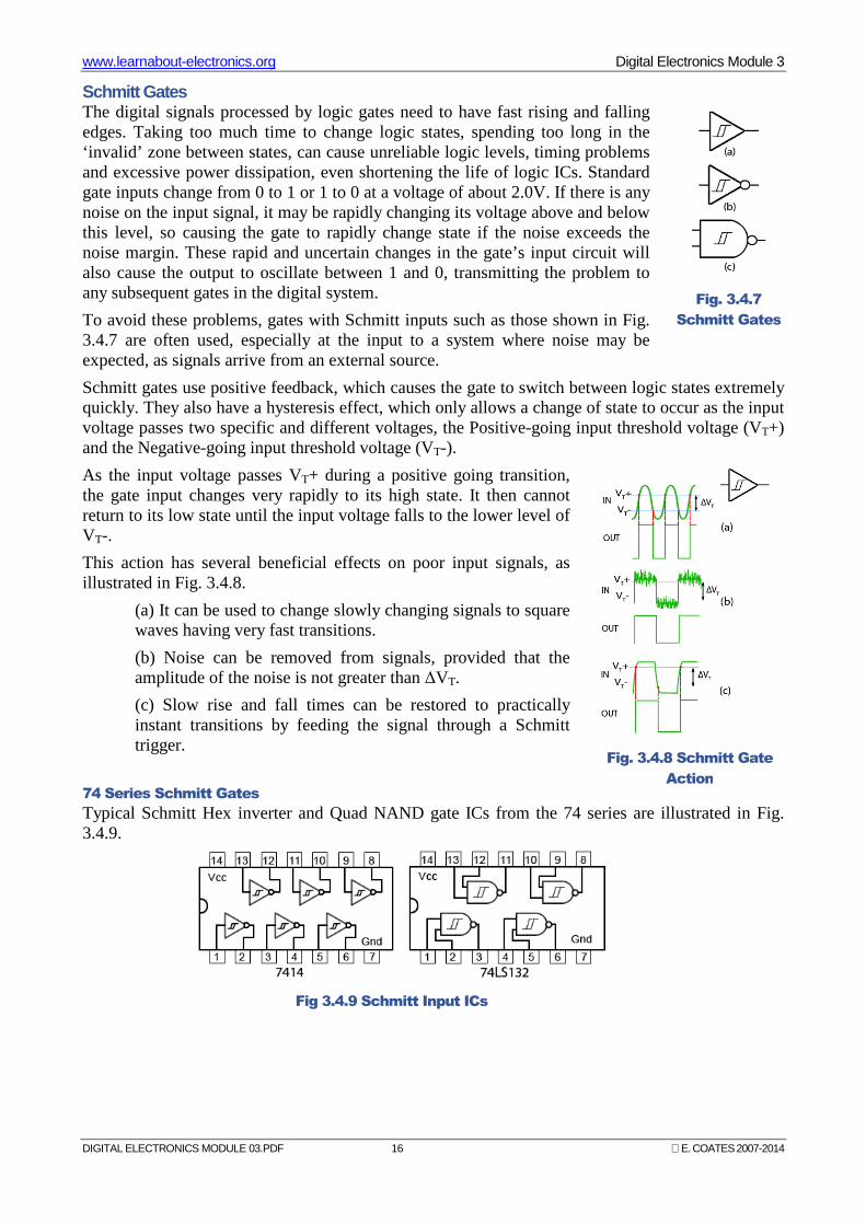
74 Series Schmitt Gates
Typical Schmitt Hex inverter and Quad NAND gate ICs from the 74 series are illustrated in Fig. 3.4.9.
Fig. 3.4.7
Schmitt Gates
Fig 3.4.9 Schmitt Input ICs
Fig. 3.4.8 Schmitt Gate
Action
www.learnabout-electronics.org Digital Electronics Module 3
DIGITAL ELECTRONICS MODULE 03.PDF 17 E. COATES 2007-2014
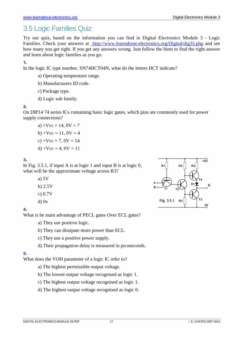
3.5 Logic Families Quiz Try our quiz, based on the information you can find in Digital Electronics Module 3 - Logic Families. Check your answers at http://www.learnabout-electronics.org/Digital/dig35.php and see how many you get right. If you get any answers wrong. Just follow the hints to find the right answer and learn about logic families as you go.
1.
In the logic IC type number, SN74HCT04N, what do the letters HCT indicate?
a) Operating temperature range.
b) Manufacturers ID code.
c) Package type.
d) Logic sub family.
2.
On DIP14 74 series ICs containing basic logic gates, which pins are commonly used for power supply connections?
a) +Vcc = 14, 0V = 7
b) +Vcc = 11, 0V = 4
c) +Vcc = 7, 0V = 14
d) +Vcc = 4, 0V = 11
3.
In Fig. 3.5.1, if input A is at logic 1 and input B is at logic 0, what will be the approximate voltage across R3?
a) 5V
b) 2.5V
c) 0.7V
d) 0v
4.
What is he main advantage of PECL gates Over ECL gates?
a) They use positive logic.
b) They can dissipate more power than ECL.
c) They use a positive power supply.
d) Their propagation delay is measured in picoseconds.
5.
What does the VOH parameter of a logic IC refer to?
a) The highest permissible output voltage.
b) The lowest output voltage recognised as logic 1.
c) The highest output voltage recognised as logic 1.
d) The highest output voltage recognised as logic 0.
www.learnabout-electronics.org Digital Electronics Module 3
DIGITAL ELECTRONICS MODULE 03.PDF 18 E. COATES 2007-2014
6.
Which of the following refers to the noise margin of a logic gate?
a) The difference between VIH and VOL
b) The difference between VOH and VOL
c) The difference between VOH and VIH
d) The difference between VIH and VIL
7.
Which of the following ICs has the largest noise margin?
a) SN74LS04n Hex inverter.
b) CD74HCT00N Quad 2 input NAND.
c) MC10EL05 2 input ECL AND/NAND.
d) SN7408N Quad 2 input TTL AND
8.
What logic function is achieved by operation an AND gate using negative logic?
a) AND.
b) NAND.
c) NOR.
d) OR.
9.
Refer to Fig. 3.5.2. Which of the following input combinations will cause output X to sink current?
a) A=0 B=0.
b) A=0 B=1.
c) A=1 B=0.
d) A=1 B=1
10.
For which of the following purposes would a Schmitt buffer be chosen?
a) To provide a high output current.
b) To enable wired logic to be used.
c) To reduce noise at the circuit input.
d) To translate logic levels when interfacing between logic families.
Related Documents