Topic 11 - 1 Nov-23-09 E4.20 Digital IC Design Topic 11 Pass Transistor Logic Peter Cheung Department of Electrical & Electronic Engineering Imperial College London URL: www.ee.ic.ac.uk/pcheung/ E-mail: [email protected] Reading:“Top-Down Pass-Transistor Logic Design”, K. Yano etc., IEEE J. of Solid-State Circuits, Vol 31, No. 6, June 1996. Topic 11 - 2 Nov-23-09 E4.20 Digital IC Design Recent d evelo pmen t i n PTL • New development by designers at Hitachi Japan in the last 10 years. • Three circuit styles proposed: Complementary Pass-transistor Logic (CPL), 1990 Double Pass-transistor Logic (DPL), 1993 Lean Integration with Pass-transistors (LEAP), 1996 • All exploit pass-transistors to implement general logic functions Topic 11 - 3 Nov-23-09 E4.20 Digital IC Design Complementary Pass-transistor Logic (CPL) “A 3.8 ns CMOS 16 x 16b Multiplier Using Complementary Pass -Transistor Logic” by K. Yano etc., IEEE J. of Solid-state Circuits, Vol 15, No 2, April 1990. • Logic network employs input signals at both gate and drain terminals. • Inputs and Outputs are always complementary. • Outputs from network prov ide strong ‘0’s but weak ‘1’s. Inverters and PMOS pull-ups provide amplification and buffering as necessary. Topic 11 - 4 Nov-23-09 E4.20 Digital IC Design Complementary Pass-transistor Logic (CPL)

Welcome message from author
This document is posted to help you gain knowledge. Please leave a comment to let me know what you think about it! Share it to your friends and learn new things together.
Transcript
8/11/2019 Topic 11 - Pass Transistor Logic
http://slidepdf.com/reader/full/topic-11-pass-transistor-logic 1/5
Topic 11 - 1Nov-23-09 E4.20 Digital IC Design
Topic 11 Pass Transistor Logic
Peter CheungDepartment of Electrical & Electronic Engineering
Imperial College London
URL: www.ee.ic.ac.uk/pcheung/E-mail: [email protected]
Reading :“Top-Down Pass-Transistor Logic Design”, K. Yano etc., IEEE J. of Solid-State Circuits, Vol 31, No. 6, June 1996.
Topic 11 - 2Nov-23-09 E4.20 Digital IC Design
Recent development in PTL
• New development by designers at Hitachi Japan
in the last 10 years.• Three circuit styles proposed:
Complementary Pass-transistor Logic (CPL), 1990 Double Pass-transistor Logic (DPL), 1993 Lean Integration with Pass-transistors (LEAP), 1996
• All exploit pass-transistors to implement general
logic functions
Topic 11 - 3Nov-23-09 E4.20 Digital IC Design
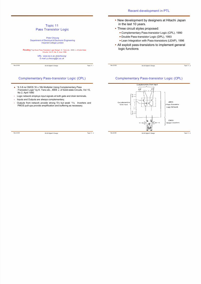
Complementary Pass-transistor Logic (CPL)
“A 3.8 ns CMOS 16 x 16b Multiplier Using Complementary Pass-Transistor Logic” by K. Yano etc., IEEE J. of Solid-state Circuits, Vol 15, No 2, April 1990.
• Logic network employs input signals at both gate and drain terminals.• Inputs and Outputs are always complementary.• Outputs from network provide strong ‘0’s but weak ‘1’s. Inverters and
PMOS pull-ups provide amplification and buffering as necessary.
Topic 11 - 4Nov-23-09 E4.20 Digital IC Design
Complementary Pass-transistor Logic (CPL)

8/11/2019 Topic 11 - Pass Transistor Logic
http://slidepdf.com/reader/full/topic-11-pass-transistor-logic 2/5

8/11/2019 Topic 11 - Pass Transistor Logic
http://slidepdf.com/reader/full/topic-11-pass-transistor-logic 3/5
Topic 11 - 9Nov-23-09 E4.20 Digital IC Design
Double Pass-transistor Logic (DPL)
“A 1.5-ns 32-b CMOS ALU in Double Pass-Transistor Logic”, M. Suzuki etc., IEEE J. of Solid-State Circuits, Vol 28, No 11, Nov., 1993
Topic 11 - 10Nov-23-09 E4.20 Digital IC Design
Basic gates in DPL
Topic 11 - 11Nov-23-09 E4.20 Digital IC Design
Why is DPL faster?
Topic 11 - 12Nov-23-09 E4.20 Digital IC Design
Sum c ircu it i n DPL
This adder circuit is extremely elegant. We have shown that for 0.6 micron technology, it offers up to 20% faster operating speed when compare with normal CMOS with only marginal increase in area.

8/11/2019 Topic 11 - Pass Transistor Logic
http://slidepdf.com/reader/full/topic-11-pass-transistor-logic 4/5
Topic 11 - 13Nov-23-09 E4.20 Digital IC Design
Carry circuit in DPL
Topic 11 - 14Nov-23-09 E4.20 Digital IC Design
Power & Speed of DPL
Topic 11 - 15Nov-23-09 E4.20 Digital IC Design
Overall add time of DPL
Topic 11 - 16Nov-23-09 E4.20 Digital IC Design
Lean Integration with Pass-Transis tor (LEAP)
“Top-Down Pass-Transistor Logic Design”, K. Yano etc., IEEE J. of Solid-State Circuits, Vol 31, No. 6, June 1996.
• It eliminated the need for keeping a large cell library by replacing a library of 61 basic cells with a new set of THREE library cells called Y1,
Y2 and Y3, and 4 inverters of different drive strength.

8/11/2019 Topic 11 - Pass Transistor Logic
http://slidepdf.com/reader/full/topic-11-pass-transistor-logic 5/5
Related Documents