Latch circuits This worksheet and all related files are licensed under the Creative Commons Attribution License, version 1.0. To view a copy of this license, visit http://creativecommons.org/licenses/by/1.0/, or send a letter to Creative Commons, 559 Nathan Abbott Way, Stanford, California 94305, USA. The terms and conditions of this license allow for free copying, distribution, and/or modification of all licensed works by the general public. Resources and methods for learning about these subjects (list a few here, in preparation for your research): 1

Welcome message from author
This document is posted to help you gain knowledge. Please leave a comment to let me know what you think about it! Share it to your friends and learn new things together.
Transcript
Latch circuits
This worksheet and all related files are licensed under the Creative Commons Attribution License,version 1.0. To view a copy of this license, visit http://creativecommons.org/licenses/by/1.0/, or send aletter to Creative Commons, 559 Nathan Abbott Way, Stanford, California 94305, USA. The terms andconditions of this license allow for free copying, distribution, and/or modification of all licensed works bythe general public.
Resources and methods for learning about these subjects (list a few here, in preparation for yourresearch):
1
Questions
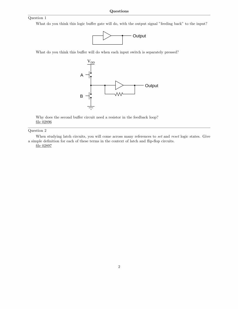
Question 1
What do you think this logic buffer gate will do, with the output signal ”feeding back” to the input?
Output
What do you think this buffer will do when each input switch is separately pressed?
Output
VDD
A
B
Why does the second buffer circuit need a resistor in the feedback loop?file 02896
Question 2
When studying latch circuits, you will come across many references to set and reset logic states. Givea simple definition for each of these terms in the context of latch and flip-flop circuits.
file 02897
2
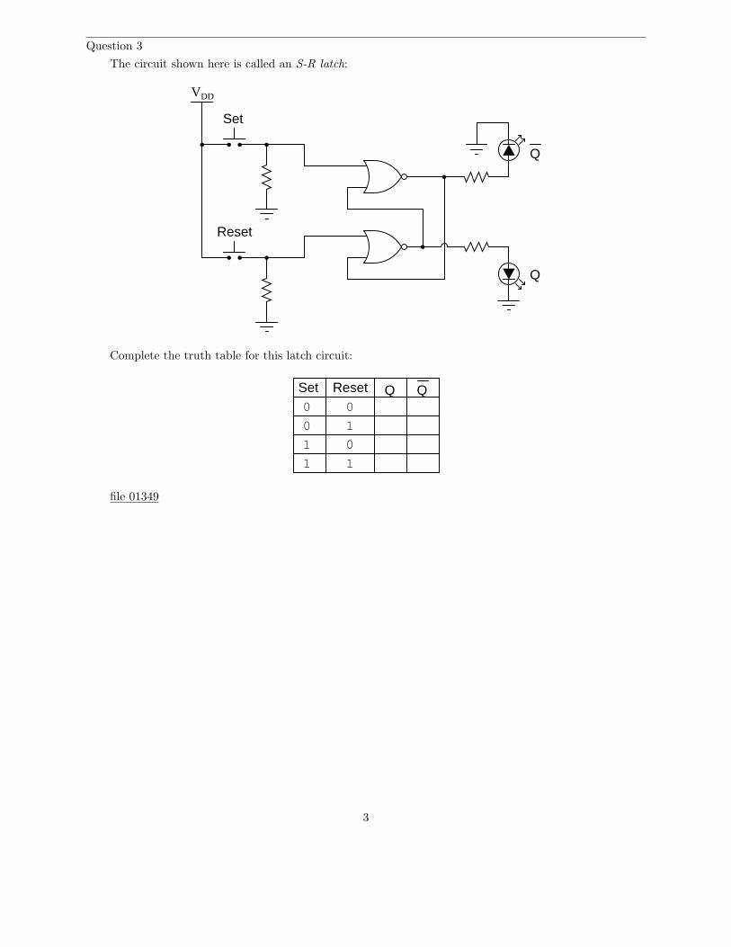
Question 3
The circuit shown here is called an S-R latch:
VDD
Set
Reset
Q
Q
Complete the truth table for this latch circuit:
Set Reset0
01
1 1
Q Q
0 1
0
file 01349
3
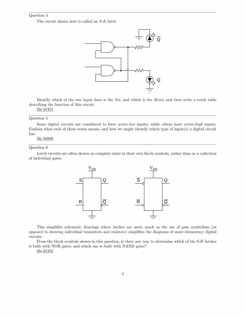
Question 4
The circuit shown here is called an S-R latch:
Q
Q
Identify which of the two input lines is the Set, and which is the Reset, and then write a truth tabledescribing the function of this circuit.
file 01351
Question 5
Some digital circuits are considered to have active-low inputs, while others have active-high inputs.Explain what each of these terms means, and how we might identify which type of input(s) a digital circuithas.
file 02898
Question 6
Latch circuits are often drawn as complete units in their own block symbols, rather than as a collectionof individual gates:
S Q
QR
S
R
Q
Q
VDD VDD
This simplifies schematic drawings where latches are used, much as the use of gate symbolism (asopposed to drawing individual transistors and resistors) simplifies the diagrams of more elementary digitalcircuits.
From the block symbols shown in this question, is there any way to determine which of the S-R latchesis built with NOR gates, and which one is built with NAND gates?
file 01352
4
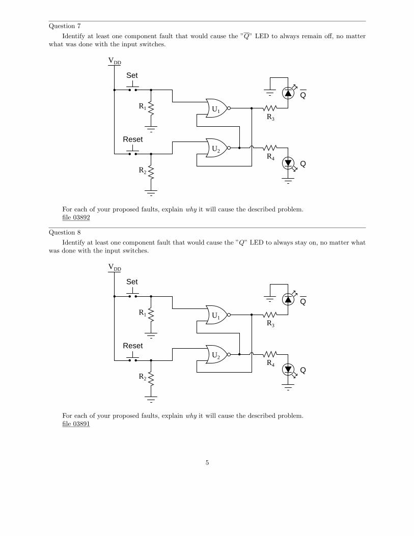
Question 7
Identify at least one component fault that would cause the ”Q” LED to always remain off, no matterwhat was done with the input switches.
VDD
Set
Reset
Q
QR1
R2
U1
U2
R3
R4
For each of your proposed faults, explain why it will cause the described problem.file 03892
Question 8
Identify at least one component fault that would cause the ”Q” LED to always stay on, no matter whatwas done with the input switches.
VDD
Set
Reset
Q
QR1
R2
U1
U2
R3
R4
For each of your proposed faults, explain why it will cause the described problem.file 03891
5
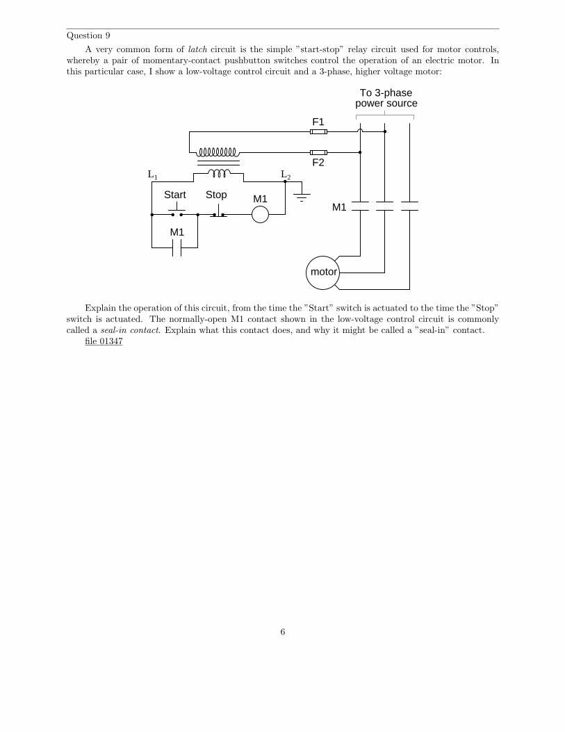
Question 9
A very common form of latch circuit is the simple ”start-stop” relay circuit used for motor controls,whereby a pair of momentary-contact pushbutton switches control the operation of an electric motor. Inthis particular case, I show a low-voltage control circuit and a 3-phase, higher voltage motor:
L1 L2
M1
M1
Start StopM1
motor
To 3-phasepower source
F1
F2
Explain the operation of this circuit, from the time the ”Start” switch is actuated to the time the ”Stop”switch is actuated. The normally-open M1 contact shown in the low-voltage control circuit is commonlycalled a seal-in contact. Explain what this contact does, and why it might be called a ”seal-in” contact.
file 01347
6
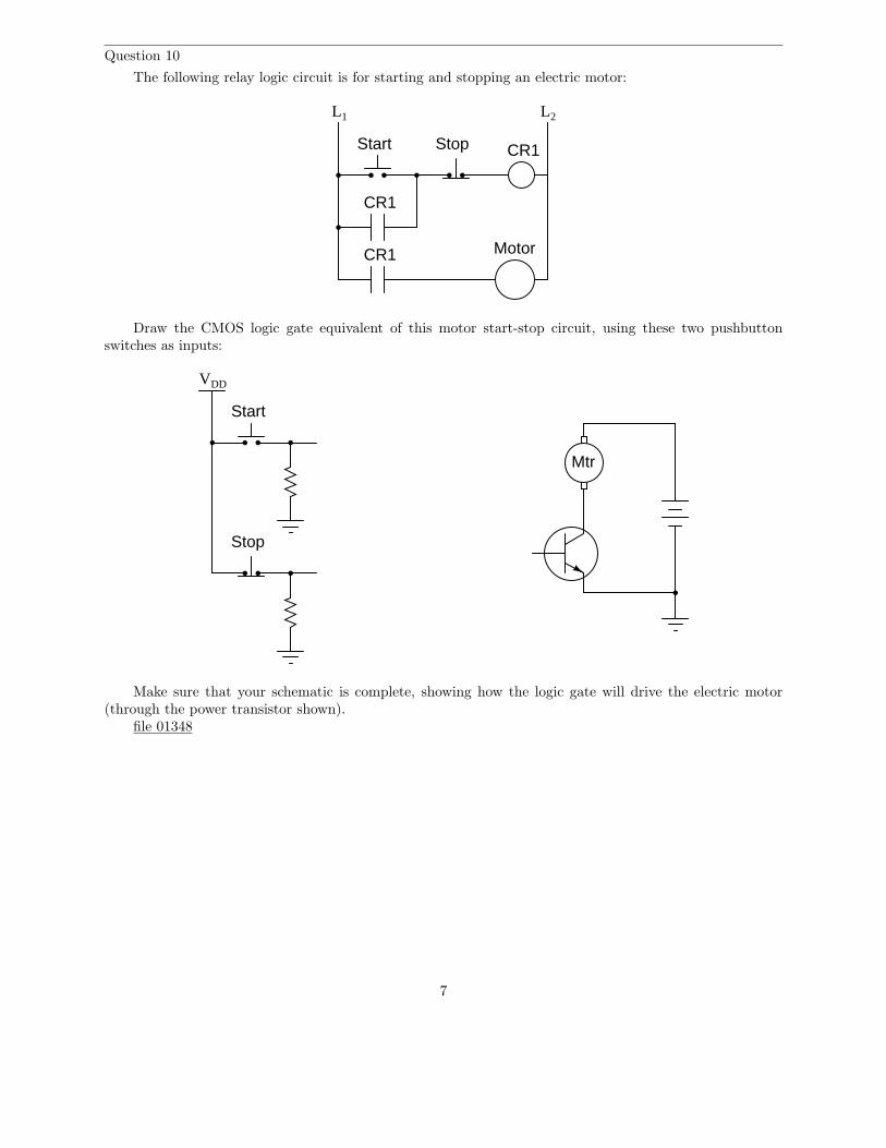
Question 10
The following relay logic circuit is for starting and stopping an electric motor:
L1 L2
CR1
CR1
CR1 Motor
Start Stop
Draw the CMOS logic gate equivalent of this motor start-stop circuit, using these two pushbuttonswitches as inputs:
Start
Stop
VDD
Mtr
Make sure that your schematic is complete, showing how the logic gate will drive the electric motor(through the power transistor shown).
file 01348
7
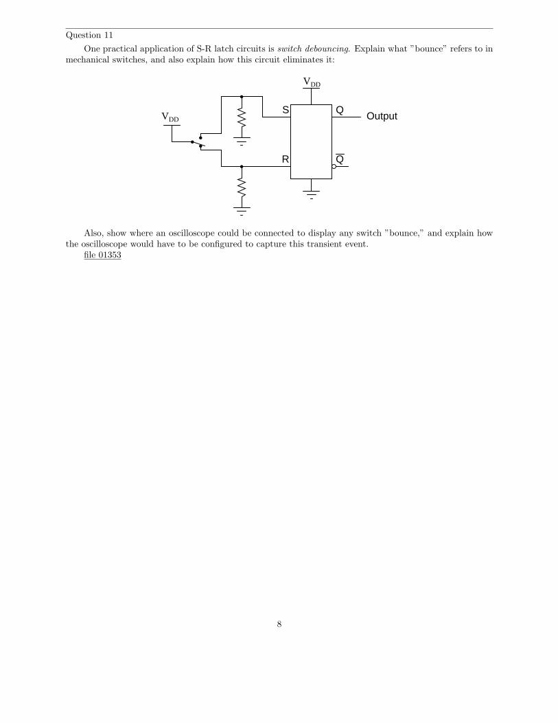
Question 11
One practical application of S-R latch circuits is switch debouncing. Explain what ”bounce” refers to inmechanical switches, and also explain how this circuit eliminates it:
S Q
QR
VDD
VDD Output
Also, show where an oscilloscope could be connected to display any switch ”bounce,” and explain howthe oscilloscope would have to be configured to capture this transient event.
file 01353
8
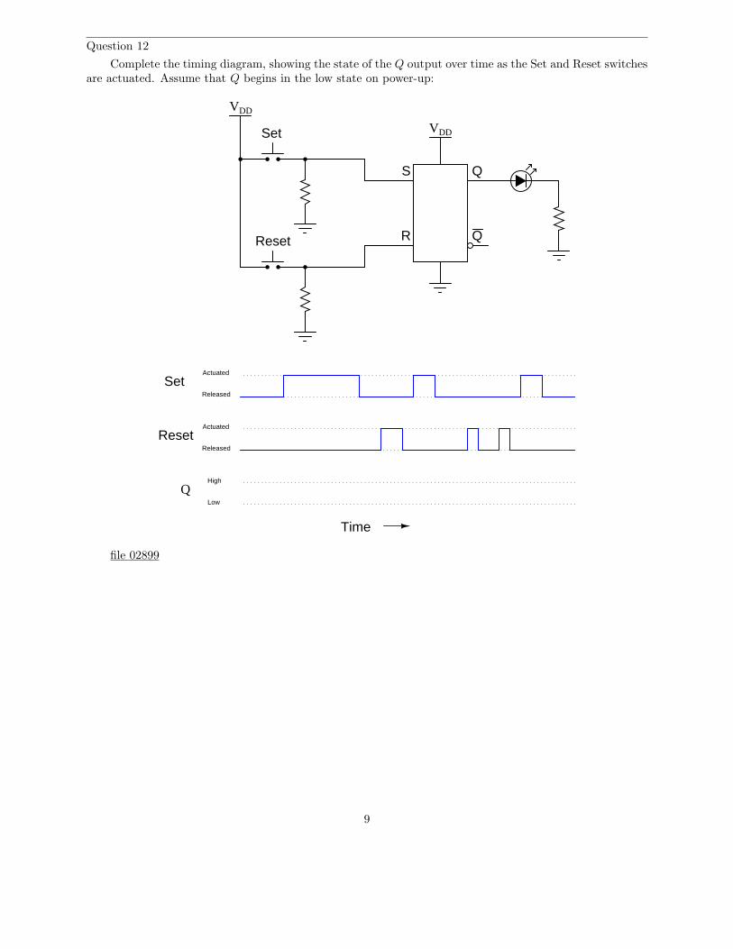
Question 12
Complete the timing diagram, showing the state of the Q output over time as the Set and Reset switchesare actuated. Assume that Q begins in the low state on power-up:
VDD
S Q
QR
Set
Reset
VDD
SetActuated
Released
Actuated
Released
Reset
QHigh
Low
Time
file 02899
9
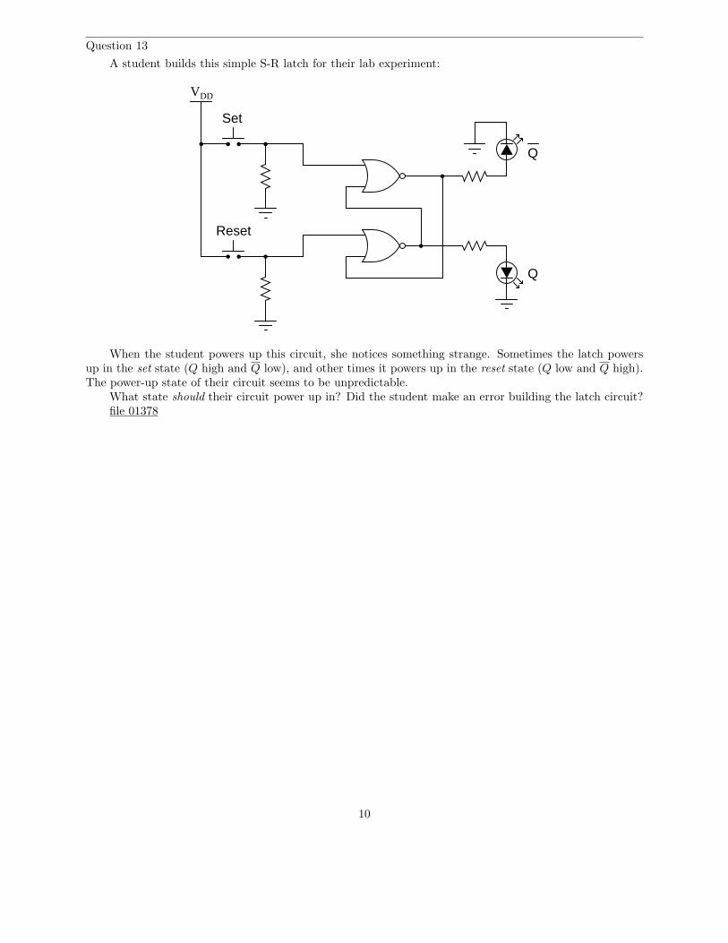
Question 13
A student builds this simple S-R latch for their lab experiment:
VDD
Set
Reset
Q
Q
When the student powers up this circuit, she notices something strange. Sometimes the latch powersup in the set state (Q high and Q low), and other times it powers up in the reset state (Q low and Q high).The power-up state of their circuit seems to be unpredictable.
What state should their circuit power up in? Did the student make an error building the latch circuit?file 01378
10
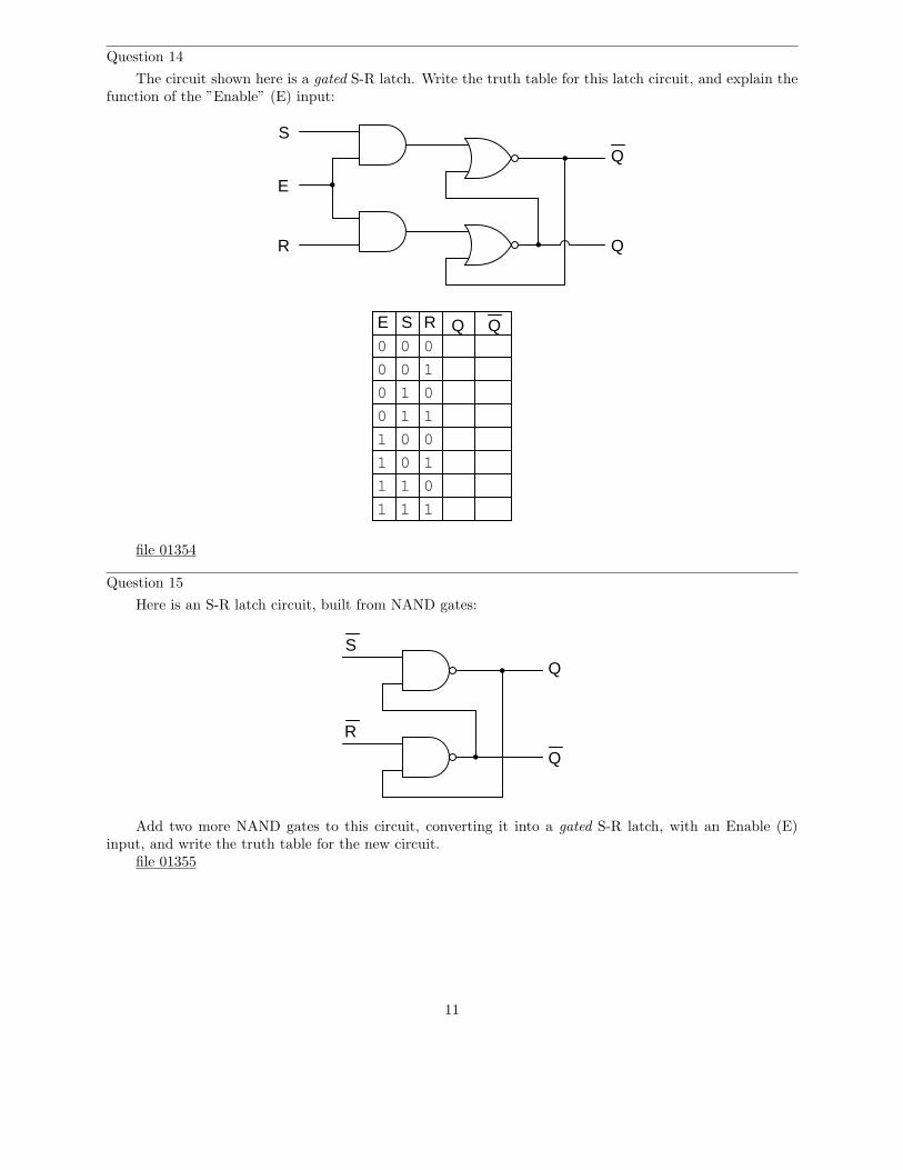
Question 14
The circuit shown here is a gated S-R latch. Write the truth table for this latch circuit, and explain thefunction of the ”Enable” (E) input:
Q
QS
R
E
E S R Q Q0
1
0 0
0 0
0
0
1
1
1
1
0
0
1
1
1
1
1
0
1
0
1
0
file 01354
Question 15
Here is an S-R latch circuit, built from NAND gates:
Q
QS
R
Add two more NAND gates to this circuit, converting it into a gated S-R latch, with an Enable (E)input, and write the truth table for the new circuit.
file 01355
11
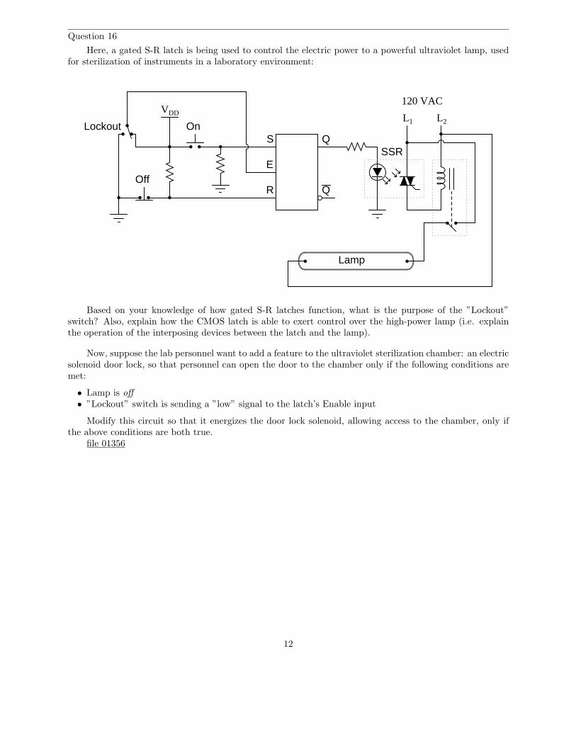
Question 16
Here, a gated S-R latch is being used to control the electric power to a powerful ultraviolet lamp, usedfor sterilization of instruments in a laboratory environment:
S Q
QR
E
VDD
Lockout On
Off
L1 L2
SSR
Lamp
120 VAC
Based on your knowledge of how gated S-R latches function, what is the purpose of the ”Lockout”switch? Also, explain how the CMOS latch is able to exert control over the high-power lamp (i.e. explainthe operation of the interposing devices between the latch and the lamp).
Now, suppose the lab personnel want to add a feature to the ultraviolet sterilization chamber: an electricsolenoid door lock, so that personnel can open the door to the chamber only if the following conditions aremet:
• Lamp is off
• ”Lockout” switch is sending a ”low” signal to the latch’s Enable input
Modify this circuit so that it energizes the door lock solenoid, allowing access to the chamber, only ifthe above conditions are both true.
file 01356
12
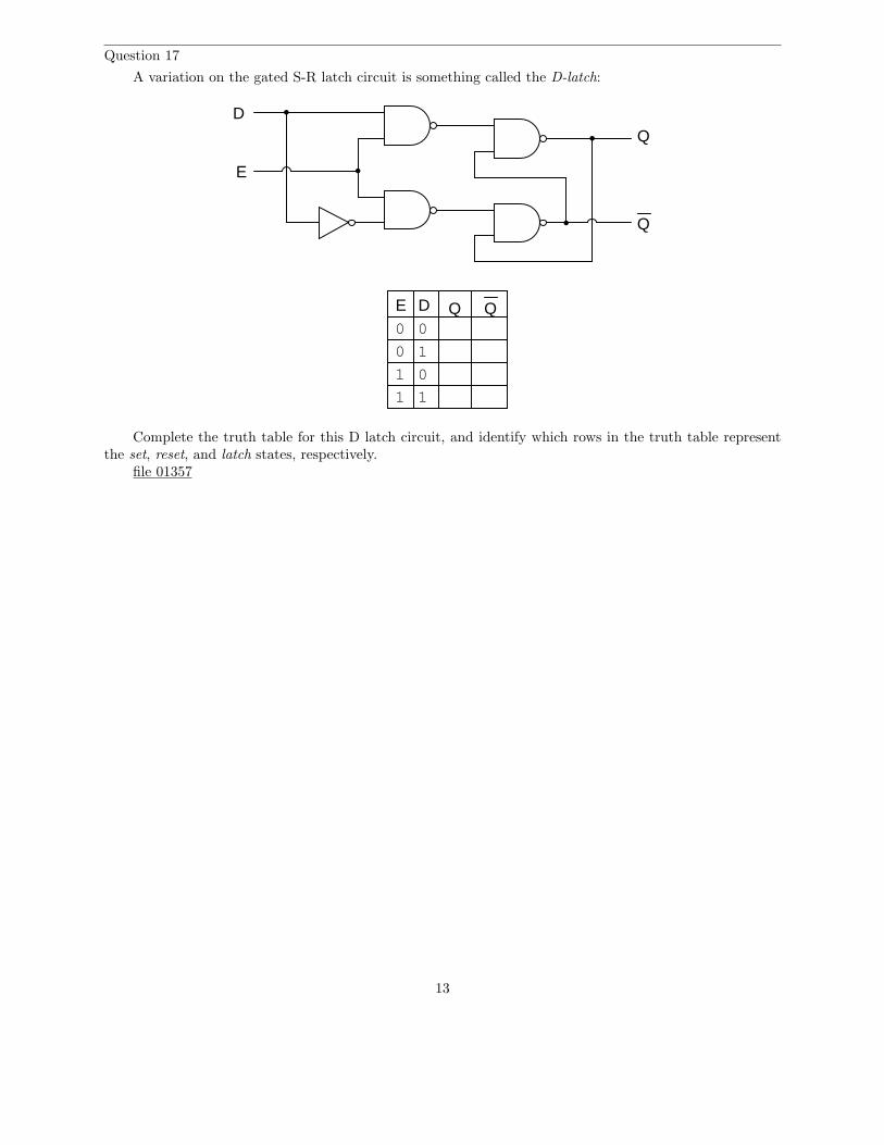
Question 17
A variation on the gated S-R latch circuit is something called the D-latch:
Q
Q
E
E Q Q0 0
0
01
1
1
1
D
D
Complete the truth table for this D latch circuit, and identify which rows in the truth table representthe set, reset, and latch states, respectively.
file 01357
13
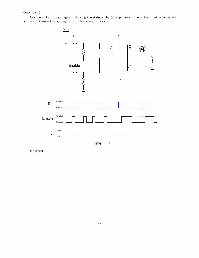
Question 18
Complete the timing diagram, showing the state of the Q output over time as the input switches areactuated. Assume that Q begins in the low state on power-up:
VDD
VDD
Actuated
Released
Actuated
Released
QHigh
Low
Time
D
D
Q
QD
E
Enable
Enable
file 02901
14
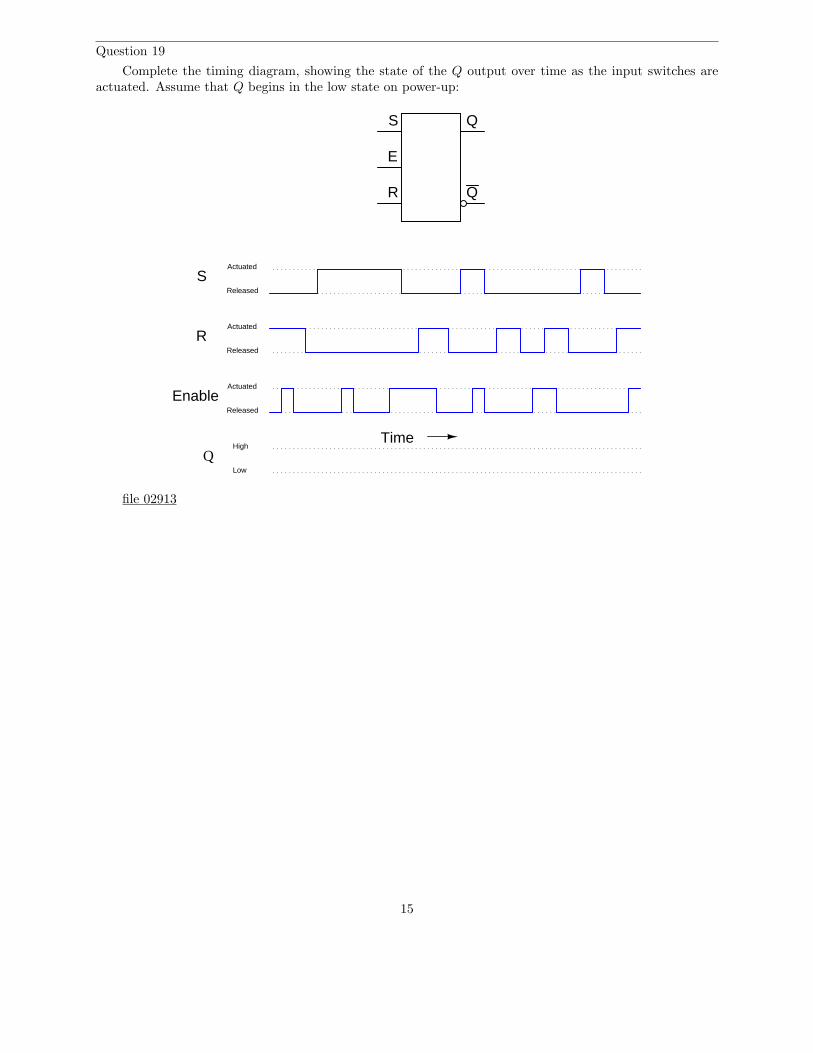
Question 19
Complete the timing diagram, showing the state of the Q output over time as the input switches areactuated. Assume that Q begins in the low state on power-up:
Actuated
Released
Actuated
Released
QHigh
Low
Time
Enable
S Q
QR
E
S
Actuated
Released
R
file 02913
15
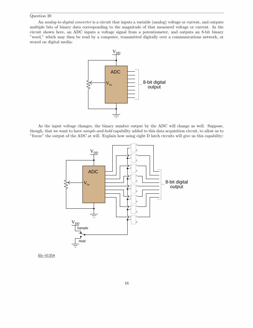
Question 20
An analog-to-digital converter is a circuit that inputs a variable (analog) voltage or current, and outputsmultiple bits of binary data corresponding to the magnitude of that measured voltage or current. In thecircuit shown here, an ADC inputs a voltage signal from a potentiometer, and outputs an 8-bit binary”word,” which may then be read by a computer, transmitted digitally over a communications network, orstored on digital media:
VDD
Vin8-bit digital
output
ADC
As the input voltage changes, the binary number output by the ADC will change as well. Suppose,though, that we want to have sample-and-hold capability added to this data acquisition circuit, to allow us to”freeze” the output of the ADC at will. Explain how using eight D latch circuits will give us this capability:
VDD
Vin8-bit digital
output
ADC
Q
QD
E
Q
QD
E
Q
QD
E
Q
QD
E
Q
QD
E
Q
QD
E
Q
QD
E
Q
QD
E
VDD
Sample
Hold
file 01358
16
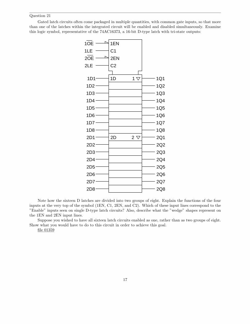
Question 21
Gated latch circuits often come packaged in multiple quantities, with common gate inputs, so that morethan one of the latches within the integrated circuit will be enabled and disabled simultaneously. Examinethis logic symbol, representative of the 74AC16373, a 16-bit D-type latch with tri-state outputs:
1EN
C1
2EN
C2
1OE
2OE
1LE
2LE
1D1D1 1Q11
1D2 1Q2
1D3 1Q3
1D4 1Q4
1D5 1Q5
1D6 1Q6
1D7 1Q7
1D8 1Q8
2D2D1 2Q1
2D2 2Q2
2
2D3 2Q3
2D4 2Q4
2D5 2Q5
2D6 2Q6
2D7 2Q7
2D8 2Q8
Note how the sixteen D latches are divided into two groups of eight. Explain the functions of the fourinputs at the very top of the symbol (1EN, C1, 2EN, and C2). Which of these input lines correspond to the”Enable” inputs seen on single D-type latch circuits? Also, describe what the ”wedge” shapes represent onthe 1EN and 2EN input lines.
Suppose you wished to have all sixteen latch circuits enabled as one, rather than as two groups of eight.Show what you would have to do to this circuit in order to achieve this goal.
file 01359
17
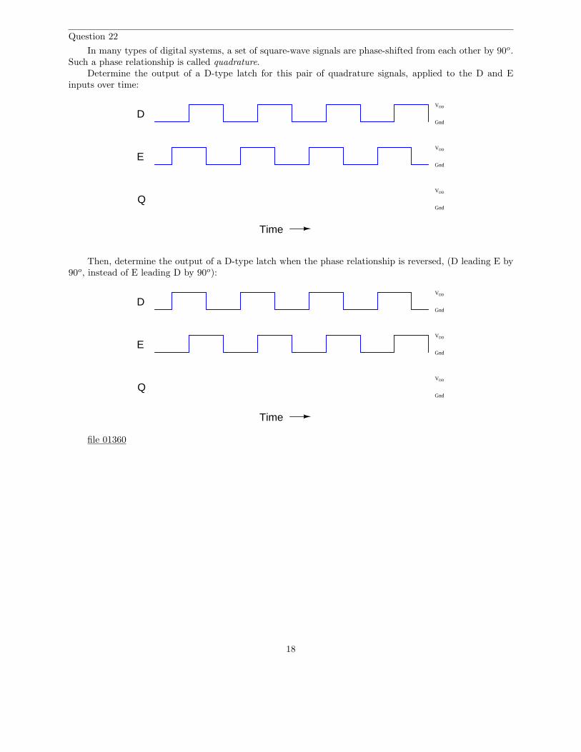
Question 22
In many types of digital systems, a set of square-wave signals are phase-shifted from each other by 90o.Such a phase relationship is called quadrature.
Determine the output of a D-type latch for this pair of quadrature signals, applied to the D and Einputs over time:
D
E
Q
VDD
Gnd
VDD
Gnd
VDD
Gnd
Time
Then, determine the output of a D-type latch when the phase relationship is reversed, (D leading E by90o, instead of E leading D by 90o):
D
E
Q
VDD
Gnd
VDD
Gnd
VDD
Gnd
Time
file 01360
18
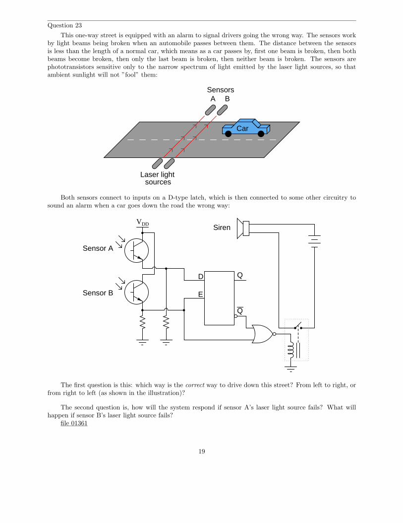
Question 23
This one-way street is equipped with an alarm to signal drivers going the wrong way. The sensors workby light beams being broken when an automobile passes between them. The distance between the sensorsis less than the length of a normal car, which means as a car passes by, first one beam is broken, then bothbeams become broken, then only the last beam is broken, then neither beam is broken. The sensors arephototransistors sensitive only to the narrow spectrum of light emitted by the laser light sources, so thatambient sunlight will not ”fool” them:
Laser lightsources
A BSensors
Car
Both sensors connect to inputs on a D-type latch, which is then connected to some other circuitry tosound an alarm when a car goes down the road the wrong way:
VDD
Sensor A
Sensor B
Q
QD
E
Siren
The first question is this: which way is the correct way to drive down this street? From left to right, orfrom right to left (as shown in the illustration)?
The second question is, how will the system respond if sensor A’s laser light source fails? What willhappen if sensor B’s laser light source fails?
file 01361
19
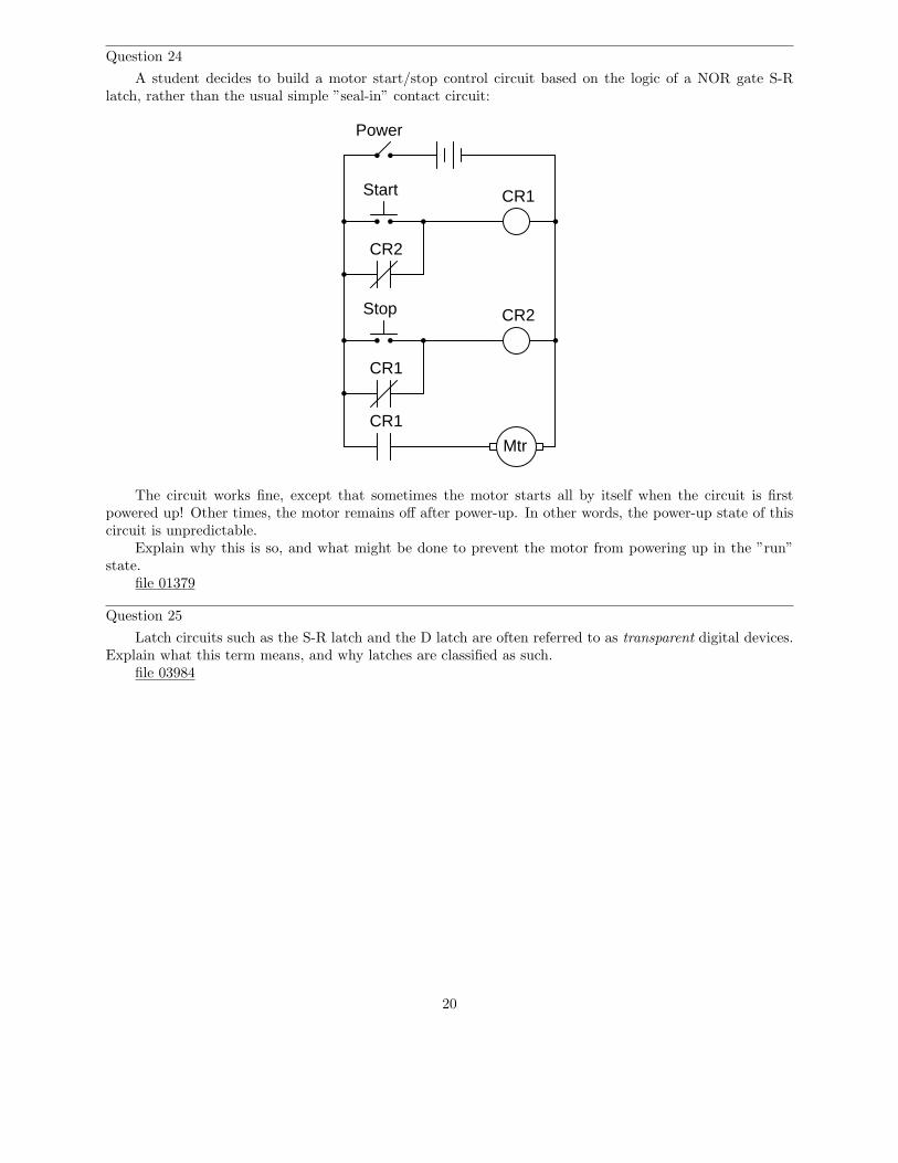
Question 24
A student decides to build a motor start/stop control circuit based on the logic of a NOR gate S-Rlatch, rather than the usual simple ”seal-in” contact circuit:
CR1Start
CR2
CR1
CR2Stop
Mtr
CR1
Power
The circuit works fine, except that sometimes the motor starts all by itself when the circuit is firstpowered up! Other times, the motor remains off after power-up. In other words, the power-up state of thiscircuit is unpredictable.
Explain why this is so, and what might be done to prevent the motor from powering up in the ”run”state.
file 01379
Question 25
Latch circuits such as the S-R latch and the D latch are often referred to as transparent digital devices.Explain what this term means, and why latches are classified as such.
file 03984
20
Question 26
Don’t just sit there! Build something!!
Learning to analyze relay circuits requires much study and practice. Typically, students practice byworking through lots of sample problems and checking their answers against those provided by the textbookor the instructor. While this is good, there is a much better way.
You will learn much more by actually building and analyzing real circuits, letting your test equipmentprovide the ”answers” instead of a book or another person. For successful circuit-building exercises, followthese steps:
1. Draw the schematic diagram for the relay circuit to be analyzed.2. Carefully build this circuit on a breadboard or other convenient medium.3. Check the accuracy of the circuit’s construction, following each wire to each connection point, and
verifying these elements one-by-one on the diagram.4. Analyze the circuit, determining all logic states for given input conditions.5. Carefully measure those logic states, to verify the accuracy of your analysis.6. If there are any errors, carefully check your circuit’s construction against the diagram, then carefully
re-analyze the circuit and re-measure.
Always be sure that the power supply voltage levels are within specification for the relay coils you planto use. I recommend using PC-board relays with coil voltages suitable for single-battery power (6 volt isgood). Relay coils draw quite a bit more current than, say, semiconductor logic gates, so use a ”lantern”size 6 volt battery for adequate operating life.
One way you can save time and reduce the possibility of error is to begin with a very simple circuit andincrementally add components to increase its complexity after each analysis, rather than building a wholenew circuit for each practice problem. Another time-saving technique is to re-use the same components in avariety of different circuit configurations. This way, you won’t have to measure any component’s value morethan once.
file 01205
21
Answers
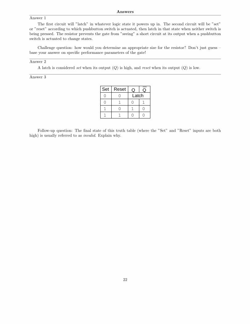
Answer 1
The first circuit will ”latch” in whatever logic state it powers up in. The second circuit will be ”set”or ”reset” according to which pushbutton switch is actuated, then latch in that state when neither switch isbeing pressed. The resistor prevents the gate from ”seeing” a short circuit at its output when a pushbuttonswitch is actuated to change states.
Challenge question: how would you determine an appropriate size for the resistor? Don’t just guess –base your answer on specific performance parameters of the gate!
Answer 2
A latch is considered set when its output (Q) is high, and reset when its output (Q) is low.
Answer 3
Set Reset0
01
1 1
Q Q
0 1
0
1
1
0 0
0
0
Latch
Follow-up question: The final state of this truth table (where the ”Set” and ”Reset” inputs are bothhigh) is usually referred to as invalid. Explain why.
22
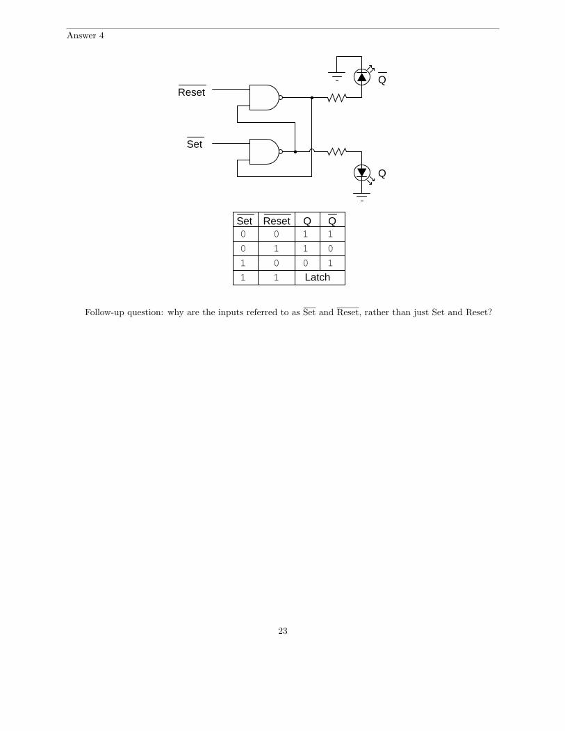
Answer 4
Q
Q
Set
Reset
Set Reset0
01
1 1
Q Q
0 1
0
Latch
1 1
1 0
10
Follow-up question: why are the inputs referred to as Set and Reset, rather than just Set and Reset?
23
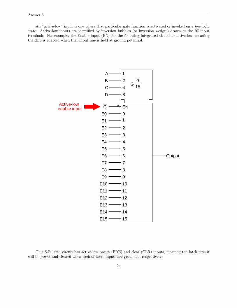
Answer 5
An ”active-low” input is one where that particular gate function is activated or invoked on a low logicstate. Active-low inputs are identified by inversion bubbles (or inversion wedges) drawn at the IC inputterminals. For example, the Enable input (EN) for the following integrated circuit is active-low, meaningthe chip is enabled when that input line is held at ground potential:
A
B
C
D
1
2
4
8
G
E0
E1
E2
E3
E4
E5
E6
E7
E8
E9
E10
E11
E12
E13
E14
E15
G015
EN
01
2
3
4
5
6
7
8
9
10
11
12
13
14
15
Output
Active-lowenable input
This S-R latch circuit has active-low preset (PRE) and clear (CLR) inputs, meaning the latch circuitwill be preset and cleared when each of these inputs are grounded, respectively:
24
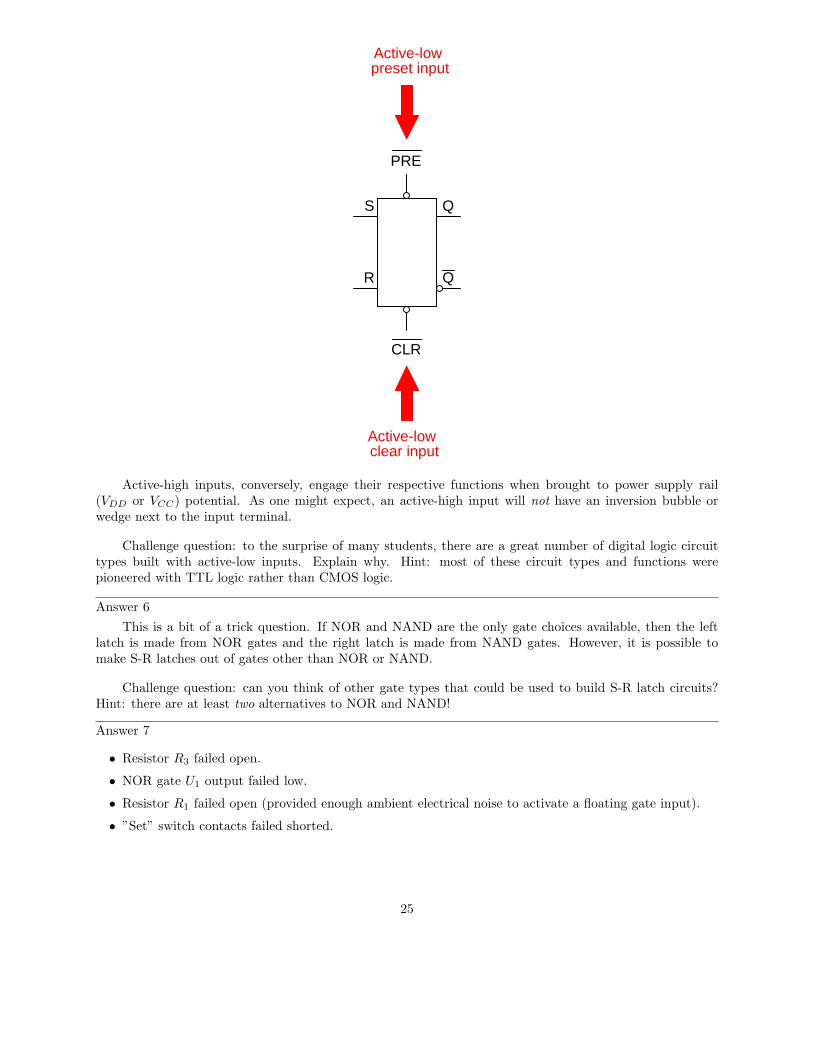
S Q
QR
PRE
CLR
preset input
clear input
Active-low
Active-low
Active-high inputs, conversely, engage their respective functions when brought to power supply rail(VDD or VCC) potential. As one might expect, an active-high input will not have an inversion bubble orwedge next to the input terminal.
Challenge question: to the surprise of many students, there are a great number of digital logic circuittypes built with active-low inputs. Explain why. Hint: most of these circuit types and functions werepioneered with TTL logic rather than CMOS logic.
Answer 6
This is a bit of a trick question. If NOR and NAND are the only gate choices available, then the leftlatch is made from NOR gates and the right latch is made from NAND gates. However, it is possible tomake S-R latches out of gates other than NOR or NAND.
Challenge question: can you think of other gate types that could be used to build S-R latch circuits?Hint: there are at least two alternatives to NOR and NAND!
Answer 7
• Resistor R3 failed open.
• NOR gate U1 output failed low.
• Resistor R1 failed open (provided enough ambient electrical noise to activate a floating gate input).
• ”Set” switch contacts failed shorted.
25
Answer 8
• NOR gate U2 output failed high.
• Wire break between ”Reset” switch and resistor R2 (although if this was the only fault it may allow theQ LED to energize at power-up, just not de-energize after the ”Set” button had been pressed).
Follow-up question: explain why the nature of the problem rules out the possibility of the only faultbeing something related to the feedback connections between U1 and U2.
Answer 9
Even though the ”Start” and ”Stop” switches are momentary, the ”seal-in” contact makes the circuitlatch in one of two states: either motor energized or motor de-energized.
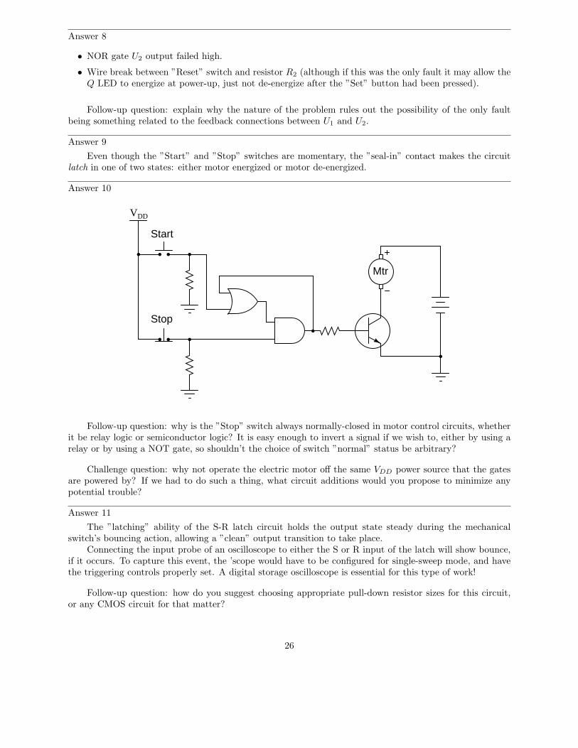
Answer 10
Start
Stop
VDD
Mtr
Follow-up question: why is the ”Stop” switch always normally-closed in motor control circuits, whetherit be relay logic or semiconductor logic? It is easy enough to invert a signal if we wish to, either by using arelay or by using a NOT gate, so shouldn’t the choice of switch ”normal” status be arbitrary?
Challenge question: why not operate the electric motor off the same VDD power source that the gatesare powered by? If we had to do such a thing, what circuit additions would you propose to minimize anypotential trouble?
Answer 11
The ”latching” ability of the S-R latch circuit holds the output state steady during the mechanicalswitch’s bouncing action, allowing a ”clean” output transition to take place.
Connecting the input probe of an oscilloscope to either the S or R input of the latch will show bounce,if it occurs. To capture this event, the ’scope would have to be configured for single-sweep mode, and havethe triggering controls properly set. A digital storage oscilloscope is essential for this type of work!
Follow-up question: how do you suggest choosing appropriate pull-down resistor sizes for this circuit,or any CMOS circuit for that matter?
26
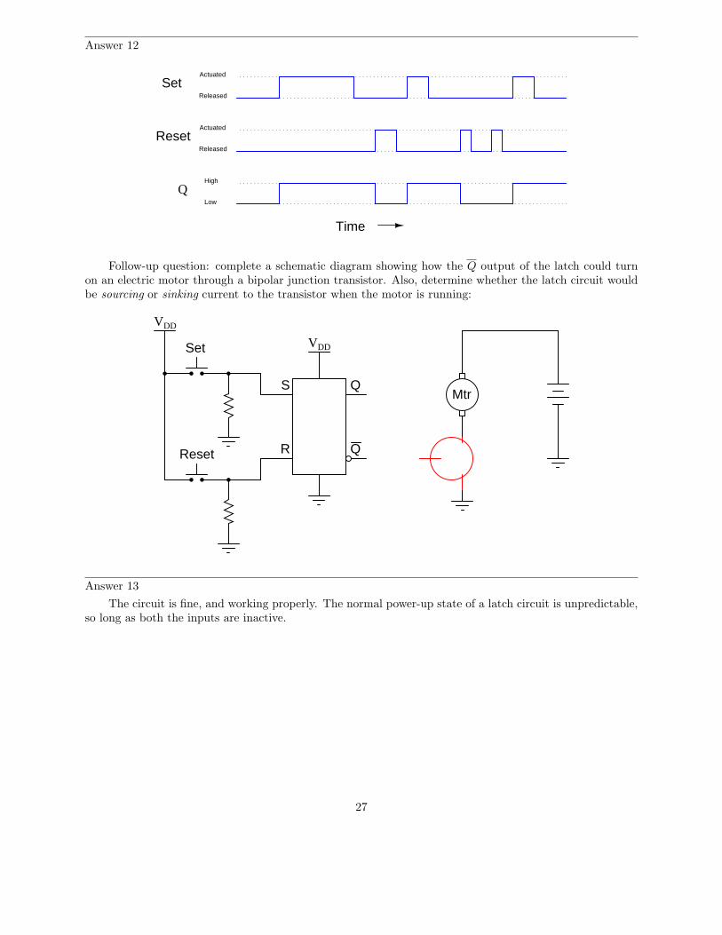
Answer 12
SetActuated
Released
Actuated
Released
Reset
QHigh
Low
Time
Follow-up question: complete a schematic diagram showing how the Q output of the latch could turnon an electric motor through a bipolar junction transistor. Also, determine whether the latch circuit wouldbe sourcing or sinking current to the transistor when the motor is running:
VDD
S Q
QR
Set
Reset
VDD
Mtr
Answer 13
The circuit is fine, and working properly. The normal power-up state of a latch circuit is unpredictable,so long as both the inputs are inactive.
27
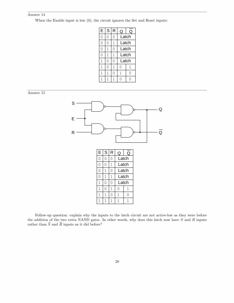
Answer 14
When the Enable input is low (0), the circuit ignores the Set and Reset inputs:
E S R Q Q0
1
0 0
0 0
0
0
1
1
1
1
0
0
1
1
1
1
1
0
1
0
1
0
LatchLatchLatchLatchLatch0 1
1 0
00
Answer 15
Q
QS
R
E
E S R Q Q0
1
0 0
0 0
0
0
1
1
1
1
0
0
1
1
1
1
1
0
1
0
1
0
LatchLatchLatchLatchLatch0 1
1 0
1 1
Follow-up question: explain why the inputs to the latch circuit are not active-low as they were beforethe addition of the two extra NAND gates. In other words, why does this latch now have S and R inputsrather than S and R inputs as it did before?
28
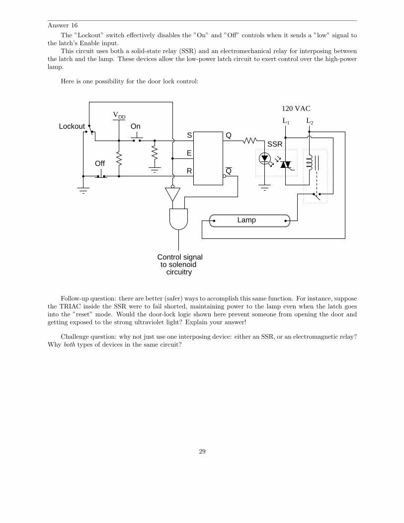
Answer 16
The ”Lockout” switch effectively disables the ”On” and ”Off” controls when it sends a ”low” signal tothe latch’s Enable input.
This circuit uses both a solid-state relay (SSR) and an electromechanical relay for interposing betweenthe latch and the lamp. These devices allow the low-power latch circuit to exert control over the high-powerlamp.
Here is one possibility for the door lock control:
S Q
QR
E
VDD
Lockout On
Off
L1 L2
SSR
Lamp
120 VAC
Control signalto solenoid
circuitry
Follow-up question: there are better (safer) ways to accomplish this same function. For instance, supposethe TRIAC inside the SSR were to fail shorted, maintaining power to the lamp even when the latch goesinto the ”reset” mode. Would the door-lock logic shown here prevent someone from opening the door andgetting exposed to the strong ultraviolet light? Explain your answer!
Challenge question: why not just use one interposing device: either an SSR, or an electromagnetic relay?Why both types of devices in the same circuit?
29
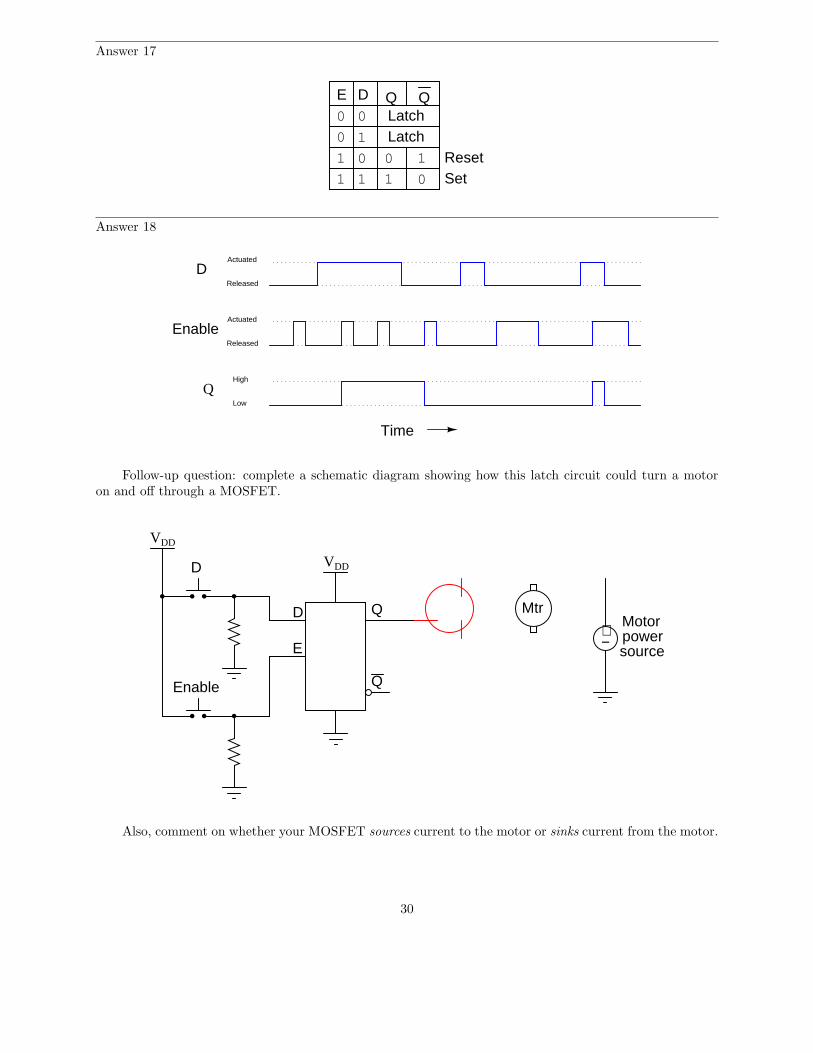
Answer 17
E Q Q0 0
0
01
1
1
1
DLatchLatch
1
1
0
0
ResetSet
Answer 18
Actuated
Released
Actuated
Released
QHigh
Low
Time
D
Enable
Follow-up question: complete a schematic diagram showing how this latch circuit could turn a motoron and off through a MOSFET.
VDD
VDDD
Q
QD
E
Enable
Mtr
+−
Motorpowersource
Also, comment on whether your MOSFET sources current to the motor or sinks current from the motor.
30
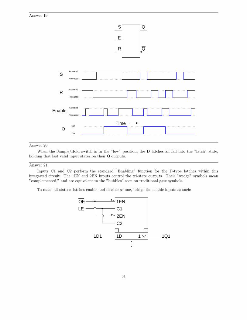
Answer 19
Actuated
Released
Actuated
Released
QHigh
Low
Time
Enable
S Q
QR
E
S
Actuated
Released
R
Answer 20
When the Sample/Hold switch is in the ”low” position, the D latches all fall into the ”latch” state,holding that last valid input states on their Q outputs.
Answer 21
Inputs C1 and C2 perform the standard ”Enabling” function for the D-type latches within thisintegrated circuit. The 1EN and 2EN inputs control the tri-state outputs. Their ”wedge” symbols mean”complemented,” and are equivalent to the ”bubbles” seen on traditional gate symbols.
To make all sixteen latches enable and disable as one, bridge the enable inputs as such:
1EN
C1
2EN
C2
1D1D1 1Q11
OE
LE
. . .
31
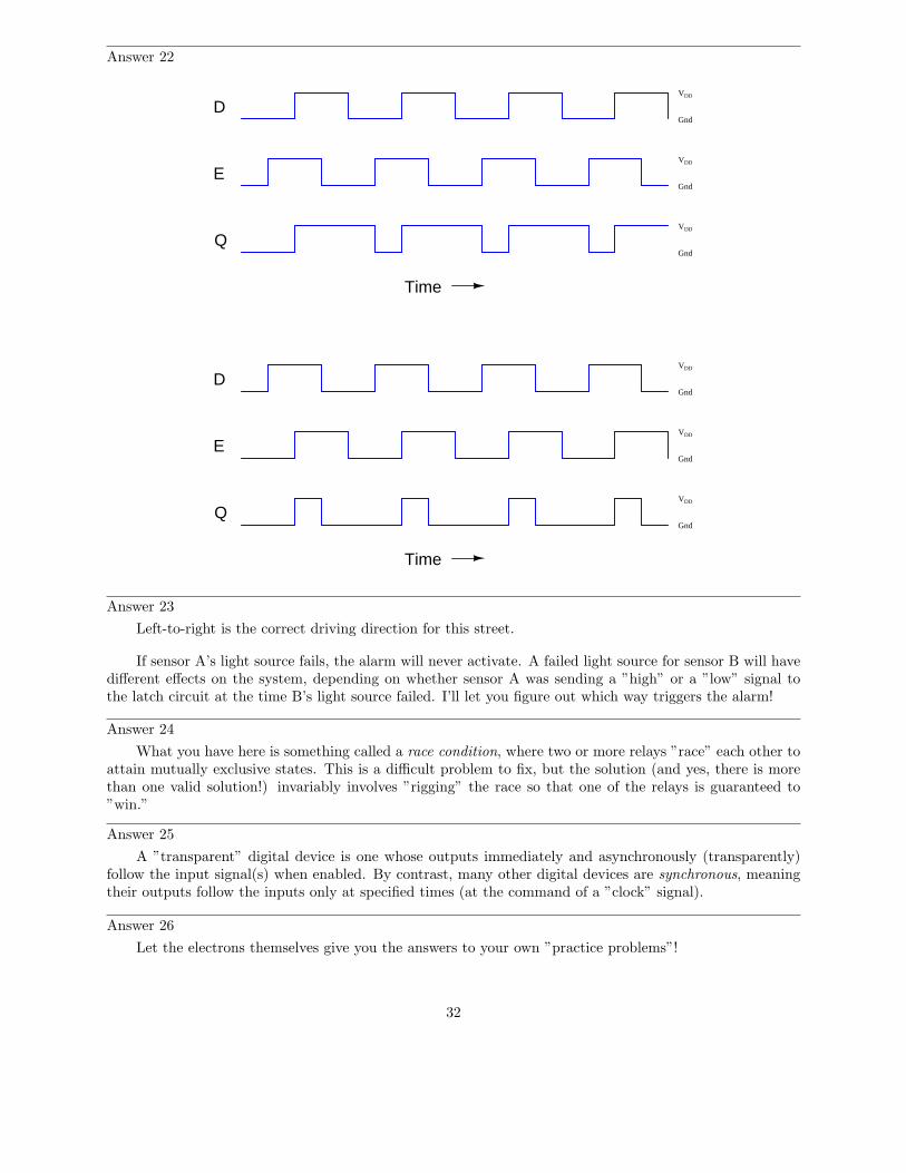
Answer 22
D
E
Q
VDD
Gnd
VDD
Gnd
VDD
Gnd
Time
D
E
Q
VDD
Gnd
VDD
Gnd
VDD
Gnd
Time
Answer 23
Left-to-right is the correct driving direction for this street.
If sensor A’s light source fails, the alarm will never activate. A failed light source for sensor B will havedifferent effects on the system, depending on whether sensor A was sending a ”high” or a ”low” signal tothe latch circuit at the time B’s light source failed. I’ll let you figure out which way triggers the alarm!
Answer 24
What you have here is something called a race condition, where two or more relays ”race” each other toattain mutually exclusive states. This is a difficult problem to fix, but the solution (and yes, there is morethan one valid solution!) invariably involves ”rigging” the race so that one of the relays is guaranteed to”win.”
Answer 25
A ”transparent” digital device is one whose outputs immediately and asynchronously (transparently)follow the input signal(s) when enabled. By contrast, many other digital devices are synchronous, meaningtheir outputs follow the inputs only at specified times (at the command of a ”clock” signal).
Answer 26
Let the electrons themselves give you the answers to your own ”practice problems”!
32
Notes
Notes 1
This is a very crude sort of latch circuit, but it is easier to understand than the typical cross-connectedNOR or NAND gate latches commonly introduced to circuits. One of the major ideas in this question isthe concept of positive feedback, and how this form of feedback leads to hysteretic behavior. If appropriate,refer your students to SCRs and other thyristors as previous examples of hysteretic devices based on positivefeedback.
Notes 2
Having a consistent definition for ”set” and ”reset” is important, especially as students study multiplelatch circuit topologies and active-low inputs!
Notes 3
The ”latch” state is the most interesting in this circuit. Discuss what this means with your students,especially since it is impossible to describe the ”latch” state in terms of fixed 1’s and 0’s.
Notes 4
The ”latch” state is the most interesting in this circuit. Discuss what this means with your students,especially since it is impossible to describe the ”latch” state in terms of fixed 1’s and 0’s. Also ask yourstudents to identify the ”invalid” state of this latch circuit, and to explain why it is called ”invalid”.
Discuss the active-low nature of this latch circuit’s inputs. Explain to your students that many digitalfunctions have active-low inputs, and that it is common to denote those inputs by writing a Booleancomplementation bar over the input’s name.
Notes 5
Active-low inputs tend to confuse many students, hence my unusually long and descriptive answer.
Notes 6
If students become stuck on the challenge question, just whisper ”DeMorgan’s Theorem” to them andwatch what happens!
Notes 7
Latch circuits can be confusing due to their use of positive feedback. Questions such as this are importanttools for helping develop your students’ understanding of latch circuits.
Notes 8
Latch circuits can be confusing due to their use of positive feedback. Questions such as this are importanttools for helping develop your students’ understanding of latch circuits.
Notes 9
Motor ”start-stop” circuits are very common in industry, and apply to applications beyond electricmotors. Ask your students if they can think of any application for a circuit such as this.
33
Notes 10
Discuss the follow-up question with your students. Why is the ”Stop” switch always normally-closed,if we have the freedom to choose normally-open contacts? Why not standardize the pushbutton switches,making them both the same type? The answer has to do with circuit faults, and what is considered thesafest mode of failure.
I suspect many students will neglect to include the base resistor in their designs. This resistor isimportant, though, for the sake of the driving gate. You might even want to spend some class time withyour students calculating an appropriate value of resistance, given such parameters as:
• Motor ”run” current = 300 mA• Transistor β = 50• VDD = 6 volts DC
The challenge question may be too advanced for students who have not yet experienced the pains oftrying to operate power devices and logic devices off the same DC bus. Suffice it to say, it is a good designrule to keep separate DC power supplies for logic and load circuitry, even if they are the exact same voltage!
Notes 11
Many textbooks use switch debouncing as a practical example of S-R latch function, so I won’t bothergiving hints as to how this circuit works. Let the students do their own research, and let them explain it toyou during discussion.
If students need practical examples of how switch ”bouncing” can be bad, suggest digital countercircuits, where a mechanical switch causes a counter to increment (or decrement) once per actuation. If theswitch bounces, the counter will increment (or decrement) more than once per switch actuation, which isundesirable.
Oscilloscope triggering is one of those features that separates novice ’scope users from competent ’scopeusers. Anyone can learn to display a repetitive waveform on an oscilloscope with a minimum of adjustment.Many modern digital oscilloscopes even have ”auto-configure” features to lock in such waveforms for display.However, to set up triggering on one-time events requires that the user understand not only the oscilloscope’sfunctions, but also the nature of the event to be captured.
Note to your students how the Q output of the latch doesn’t go anywhere. Often, we have applicationswhere the second output of a latch is unused. Ask your students whether or not this constitutes a problem.(If you get blank stares from asking this question, remind students that unused CMOS inputs have to begrounded or tied to VDD, or else damage may occur. Ask them whether or not the same rule applies to gateoutputs.) This will be a good review of internal gate circuit construction.
Notes 12
Nothing special here in this question. Perhaps the main point is to familiarize students with the conceptof a timing diagram, and how to transfer the truth table function of a specific logic circuit to a time-domainplot.
Notes 13
Although the circuit itself is simple, the phenomenon is not. Tell your students that what they’re dealingwith here is something called a race condition, where two or more gates try to ”race” each other to reach acertain logic state. Analyze the power-up state of this circuit with your students, and they will see that anunstable condition exists when both inputs are inactive!
Notes 14
Just one more level of gating added to an S-R latch circuit!
34
Notes 15
Ask your students if they see any practical advantage to this latch circuit over a gated latch built fromNOR gates. What if they had to build a latch circuit from individual gates, rather than as a completeintegrated circuit in and of itself? Would one design be preferable over the other?
Then, ask your students to compare the truth tables of the two different types of gated latches. Is thereany difference in operation at all between the latch built with NAND gates and the latch built with NORgates?
Notes 16
The purpose of the ”Lockout” switch is fairly simple, and should be easy for the students to explain.On the other hand, the design and implementation of a door lock safety circuit is a more complex question,deserving of discussion because it involves several important and realistic considerations:
• How do we go from a simple verbal description of logical conditions (lamp off, enable low) to an actualgate circuit?
• What is the safest strategy to use in determining when it is safe to open the door?• How should the door lock logic interpose to the solenoid itself (this is not shown in the answer!)?• How would the principles of lock-out/tag-out apply to this system, if we were approaching the problem
from the perspective of maintenance personnel rather than lab (operations) personnel?
The challenge question gets students thinking in terms of real-life currents and voltages, and thelimitations of each device.
Notes 17
Since this gate does not actually have ”Set” and ”Reset” inputs, ask your students to explain whatconditions define the ”set” and ”reset” states. Note that these state labels may be applied to any type oflatch circuit.
To many of your students, this latch circuit may seem rather useless. Explain to them that this basiclatch may be used to form memory cells, with each D latch storing 1 binary bit of information! Ask yourstudents to explain, in their own words, how the latching action of this circuit constitutes a memory function.Under what condition(s) will the stored information in a D latch memory cell be lost?
Notes 18
Some students may be confused about the width of the last pulse on the Q output. Remind them thatQ follows D for as long as the Enable input is activated!
Notes 19
Have your students explain exactly how they arrived at the solution they did for the output waveform.Are they making use of a truth table for the S-R latch to figure out what happens? Are they doing it bymemory? Can they discriminate between an output state change initiated by either the Set or Reset inputsversus one initiated by the enable going high?
Notes 20
Sample-and-hold circuitry is quite common in modern data acquisition and other types of electronicsystems. In this case, sample-and-hold showcases a practical use of D latch circuits. If your studentshave not yet heard of analog-to-digital converters, it might be a good idea to discuss some of their generalprinciples. No knowledge of their internal workings is necessary in order to comprehend the circuit shownin the question, however.
35
Notes 21
This question not only introduces students to the concept of multiple latches in a single integratedcircuit, but it also shows an example of IEEE/ANSI ”block” symbolism. Your students, having become welladjusted to the idea of independent research by now, should have obtained the datasheet for this circuit(74AC16373) as part of their study. The information contained in the datasheet should prove to be quiteinformative in answering their questions about enable input functions, tri-state outputs, and the like. If theyhaven’t obtained datasheets, and cannot understand the answers to the question(s), don’t just tell them –have them look it up for themselves!
Notes 22
Students need to be proficient in analyzing pulse diagrams, especially with latch circuits (and later, withflip-flops), because these types of circuits often find application in pulse-driven systems.
Notes 23
This question is a great problem-solving exercise. Students must figure out how to set it up so that theymay apply the rules of latch circuits and gate circuits, then they must analyze it correctly! Devote plenty ofclassroom time to a discussion of this problem.
Students may show a reluctance to draw a timing diagram when they approach this problem, even whenthey realize the utility of such a diagram. Instead, many will try to figure the circuit out just by looking atit. Note the emphasis on the word ”try.” This circuit is much more difficult to figure out without a timingdiagram! Withhold your explanation of this circuit until each student shows you a timing diagram for it.Emphasize the fact that this step, although it consumes a bit of time, is actually a time-saver in the end.
It is easy as an instructor to focus so intently on teaching electronic theory that other practical mattersbecome neglected. Electronic technicians and engineers do not simply work on circuits; they work on systems
that happen to employ electronic circuits. Ultimately, nearly every electronic circuit they work with willhave some relationship to the physical world. Problem solving exercises in school must include scenariossimilar to real life, where conditions and functions other than electronics have a role in determining thesolution. Only by exposing students to problems requiring them to think beyond pure electronics will theybecome adequately prepared to meet the challenges of their future careers.
Notes 24
Analyze the power-up states of this circuit with your students, and the ”race” condition will becomeapparent. Such problems can be very difficult to locate and fix in real life, so it is good to expose studentsto them early in their education, and in contexts where the circuitry is not too confusing.
Notes 25
The term ”transparent” becomes more meaningful when latches and flip-flops are compared with oneanother.
36
Notes 26
It has been my experience that students require much practice with circuit analysis to become proficient.To this end, instructors usually provide their students with lots of practice problems to work through, andprovide answers for students to check their work against. While this approach makes students proficient incircuit theory, it fails to fully educate them.
Students don’t just need mathematical practice. They also need real, hands-on practice building circuitsand using test equipment. So, I suggest the following alternative approach: students should build their own”practice problems” with real components, and try to predict the various logic states. This way, the relaytheory ”comes alive,” and students gain practical proficiency they wouldn’t gain merely by solving Booleanequations or simplifying Karnaugh maps.
Another reason for following this method of practice is to teach students scientific method: the processof testing a hypothesis (in this case, logic state predictions) by performing a real experiment. Students willalso develop real troubleshooting skills as they occasionally make circuit construction errors.
Spend a few moments of time with your class to review some of the ”rules” for building circuits beforethey begin. Discuss these issues with your students in the same Socratic manner you would normally discussthe worksheet questions, rather than simply telling them what they should and should not do. I nevercease to be amazed at how poorly students grasp instructions when presented in a typical lecture (instructormonologue) format!
A note to those instructors who may complain about the ”wasted” time required to have students buildreal circuits instead of just mathematically analyzing theoretical circuits:
What is the purpose of students taking your course?
If your students will be working with real circuits, then they should learn on real circuits wheneverpossible. If your goal is to educate theoretical physicists, then stick with abstract analysis, by all means!But most of us plan for our students to do something in the real world with the education we give them.The ”wasted” time spent building real circuits will pay huge dividends when it comes time for them to applytheir knowledge to practical problems.
Furthermore, having students build their own practice problems teaches them how to perform primary
research, thus empowering them to continue their electrical/electronics education autonomously.In most sciences, realistic experiments are much more difficult and expensive to set up than electrical
circuits. Nuclear physics, biology, geology, and chemistry professors would just love to be able to have theirstudents apply advanced mathematics to real experiments posing no safety hazard and costing less than atextbook. They can’t, but you can. Exploit the convenience inherent to your science, and get those students
of yours practicing their math on lots of real circuits!
37
Related Documents