TRANSMITTER AND RECEIVER CIRCUITS FOR DIGITAL
FREE-SPACE OPTICAL INTERCONNECT: DESIGN
AND SIMULATION
by
KRISHNAKUMAR VENKITAPATHY, B.E.
A THESIS
IN
ELECTRICAL ENGINEERING
Submitted to the Graduate Faculty of Texas Tech University in
Partial Fulfillment of the Requirements for
the Degree of
MASTER OF SCIENCE
IN
ELECTRICAL ENGINEERING
Approved
Chairperson ot the Committee
Accepted
Dean of the Graduate School
May, 2004

ACKNOWLEDGEMENTS
First, I would like to thank my advisors. Dr. Tim Dallas and Dr. Sergey
Nikishin for their patience and carefully resttained guidance in my thesis work.
Their good nature and support have been a source of encouragement not only for
this work, but, throughout my term as a graduate student at Texas Tech
University.
I would like to thank Yagya Narayanan Sethuraman and Chintan Trehan,
both Masters Students from the Electiical Engineering Department, TTU, for
helping me with learning the different things required to accomplish this work.
I extend my special thanks to my fiiends Raquel Lim and Gangadharan
Sivaraman for their moral support during the course of this work.
I acknowledge the encouragement that I have received from all my
friends. They have been really supportive during difficult times. Finally, I thank
my mother for providing me with a good education. The support, encouragement
and love, 1 have received from my mother has been a real motivation for me and
has always inspired me to do my best.
11

TABLE OF CONTENTS
ACKNOWLEDGEMENTS
ABSTRACT
LIST OF TABLES
LIST OF FIGURES
1. INTRODUCTION 1
1.1 Primary contiibutions of this research 3
1.2.Thesis Organization 3
2. DEVICE MODELS 4
2.1 Model accuracy 4
2.1.1 CMOS device model 6
2.1.2 Design parameters and extraction 9
2.1.3 Parameter variations 10
2.1.3.1 Lot-to-lot variations 12
2.1.3.2 Transistor mismatch 12
2.1.4 Digital system performance 14
2.2 VCSEL model 14
3. RECEFVER CIRCUIT ANALYSIS AND DESIGN 1 g
3.1 Introduction 18
3.2 Previous work in optical receivers 20
3.2.1 Optimization 20
3.3 Receiver circuit design 21
ui
11
111
Vlll
IX

3.3.1 Gain stage 25
3.3.1.1 Gain stage options 2 5
3.3.1.2 RCS inverter design 28
3.3.2 Feedback resistor 31
3.3.3 Decision circuit 32
3.3.4 Digital Buffer 35
3.3.5 Data Latch 3^
3.4 Receiver Model 3-7
3.4.1 Transimpedance amplifier 3 7
3.4.2 Voltage amplifier 43
3.4.3 Bk Rate 44
3.4.4 Transimpedance Gain 45
3.4.5 Power 47
3.4.6 Size 47
48
56
3.5 Noise
3.5.1 Bk Error Rate
4. OPTIMIZATION AND SIMULATION 59
4.1 Approximate analysis 59
4.2 Receiver simulation description 60
4.2.1 Receiver Simulation 62
4.2.2 Receiver Schematics 62
4.2.3 Simulation results 69
IV

4.3 Transmitter circuit 77
5 SUMMARY 79
BIBLIOGRAPHY 81
ABSTRACT
Modem computer processors run at a speed of many GHz but the off-chip
interface mns only at a speed of a few hundred MHz. A key reason for this difference,
and a problem for computing in general, is that the interface connection speeds are not
able to keep up with the increase in processor speeds. This is due to design issues
associated with electrical wires and their underlying physical properties. Due to the
capacity limitations of electrical wires, all long distance communication is now done via
optics. Optics has many features, beyond those exploited in long distance fiber
communications, which make it interesting for connections at short distance, including
dense optical interconnections directly to silicon integrated circuit chips. Optical
interconnects to chips have been studied for a long time. This study started with the
seminal paper by Goodman [1]. Since then, many authors have addressed the benefits and
limitations of optical interconnects ([2][3][4][5][6][7][8][9][10][11]).
Development of CMOS transmitter and receiver circuits is required for integrating
digital free space optical interconnects (FSOI) with the mainsfream VLSI computing
system. These circuks are the interface between on-chip digital signals and the off-chip
optical signals, and thus their design and optimization is vety important. In the analog
regime, their noise, frequency response and stability are taken as important design
criteria. In the digital regime, they must be fast, small, low power and reliable. Meeting
these design criteria makes the design more complicated.
We will first examine the analysis and design of fransmitter and receiver circuits
for FSOI. Then, we will optimize the receiver circuit for various design parameters. Then
vi

we will design the fransmitter circuit based on the receiver circuit requirements. We will
finally conclude by providing the simulation results of the total link.
vu
LIST OF TABLES
2.1 CMOS technology parameters 9
2.2 Matching proportionality constants for different CMOS processes 13
2.3 CMOS digital technology parameters 14
2.4 VCSEL parameters used in this analysis, from [24,25] 16
3.1 Rise time co-efficients 45
3.2 Calculated noise coefficients for different receiver configurations 55
4.1 Input parameters 60
4.2 Constants used in analysis 61
4.3 Simulated receiver design parameters 63
4.4 Simulated receiver transistor widths (0.5 um Technology) 64
Vll l
LIST OF FIGURES
2.1 Small-signal transistor model.
2.2 Variation of gate-source and gate-drain capacitances versus VGS-
2.3 MOS device capacitance-decomposition of drain-bulk capacitance 8 into bottom-plate and sidewall components
2.4 Cross-section of a VCSEL and Edge emitting devices 15
3.1 Receiver classifications: (a) low impedance, (b) transimpedance, 22 high impedance, and (d) integrate-and-dump
3.2 Transimpedance receiver block diagram 23
3.3 Effect of the current bias on amplifier voltage swing (thick arrow): 24 (a) Without current bias and (b) With current bias
3.4 Gain stage circuit design: (a) CMOS inverter, (b) current-source 27 inverter, (c) telescopic cascade, (d) folded cascade, (e) ratioed current -source inverter
3.5 Gain stage voltage bias generator 30
3.6 Feedback resistor implementation 31
3.7 The decision circuit output rise time is made equal to that of a 33 minimum sized CMOS inverter by setting the width of PMOS such that I2 - Ii = Ip.
IX

3.8 Digital buffer 35
3.9 Circuk for one-stage ttansimpedance ampUfier. 37
3.10 Pole locations in the s-plane for the maximally flat magnitude 3 8 response
3.11 Small signal circuit for the one-stage transimpedance amplifier 39
3.12 Pole locus for one-stage transimpedance amplifier as the value of Rf 41 is changed
3.13 Layout floorplan of receiver gain stage and decision circuit 47
3.14 Noise sources in the receiver 49
3.15 TIA noise model 50
3.16 VA noise model 51
3.17 Probability distribution of received values 56
4.1 Full receiver schematic for 1+0 receiver 66
4.2 Full receiver schematic for 1+1 receiver 67
4.3 Full receiver schematic for 1+2 receiver 68
4.4 (1 +0) Receiver - 1 Gbits output (. 1 mA current) 69
4.5 (1+0) Receiver - 500Mbits output (.06 mA curtent) 70

4.6 (1+0) Receiver - 500Mbits output (. 1 mA current) 71
4.7 (1+1) Receiver - 700Mbits output (.1 mA current) 72
4.8 (1+1) Receiver - 700Mbits output (.05 mA current) 73
4.9 (1+1) Receiver - 700Mbits output (.1 mA current, Rf- 2kn) 74
4.10 (1+2) Receiver - 400Mbits output (.03 mA current) 75
4.11 (1+2) Receiver - 500Mbits output (.04 mA current) 76
4.12 VCSEL fransmitter circuitry 78
XI
CHAPTER 1
INTRODUCTION
This thesis examines the design, optimization and simulation of digital free space
optical interconnects for high speed computing systems. A free space optical interconnect
(FSOI) is an optical link where the propagation medium is air. FSOI is intended to
replace electrical interconnects at the board/chip level in near future.
In recent years, optical interconnects have made a tremendous impact on the
ability to communicate over long distances. Fiber optic cabling over long distances has
enabled unprecedented data capacity for global data and telephony networks. The idea of
using fiber optics to replace wires has now slowly shifted towards communication over
short distances inside digital computers, possibly connecting directly to the silicon chips
or even for coimections on chip. Several studies have attempted to identify a break-even
line length where optical and electrical interconnect performance cross. These studies
also indicate that optical interconnects are advantageous down to the chip-to-chip level, if
not below [12].
Of-course, implementing free space optical interconnects for chips would also
face many technical challenges. If we wish seriously to impact FSOI on the chip level,
we need to be considering technologies that can allow "dense" optical interconnects at
the chip level, by which we mean at least hundreds or more likely thousands of optical
interconnects for each chip. Without such numbers, most off-chip interconnects and long
on-chip interconnects would have to remain electrical.

The continuing exponential reduction in feature sizes on electronic chips, known
as Moore's law, leads to ever larger number of faster devices at lower cost per device.
The empirically derived Rent's mle [13] relates the I/O requirement to the processing
power (K) of a chip as K°^^, indicating that I/O requirements will continue to increase.
Off-chip bandwidth can be achieved with either more pins or faster off-chip signaling.
Gigahertz off-chip signaling is a significant challenge. It suffers from signal integrity and
power dissipation issues, and cannot be scaled up to accommodate all of the predicted
bandwidth increase. As for more I/O pins, the 2003 Semiconductor Industry Association
(SIA) Roadmap predicts a grov^h in pins/unit of 11% per year, while the cost/pin drops
at 5% per year. However, there is growing acknowledgement that the interconnection
problem will be a critical limiting factor in the near future.
There are several possible approaches to such interconnection problems, and
likely, all of them will be used to some degree. Architectures could be changed to
minimize interconnection. Design approaches could put increasing emphasis on the
interconnection layout. Signaling on wires could be significantiy improved through the
use of a variety of technique, such as equalization [14]. Most important for this thesis is a
fourth approach - changing the physical means of interconnection. FSOI is a very
interesting and different physical approach to interconnection that can, in principle,
address some of the interconnection problems.

1.1 -Primarv contributions of this research
If CMOS-FSOI is to become a mainstream technology, careful analysis and
optimization of tiie supporting CMOS circuitty is required. This is not only important for
the system designer, but also for the OptoElectronic (OE) designer, for two reasons. First,
the best performance is obtained from an OE device only when the circuitry has been
optimized to support it. Second, the limitations and opportunities afforded by CMOS
circuit optimization can indicate the direction of future device research.
In the hierarchy of a system design methodology, this study is intended to fit in
between the "system/application" (top) level and the "device/technology"(bottom level),
at the "functional block"(middle level). For example, in the commercial CMOS design
world this level would be the standard cell library or IP block library. By analyzing and
optimizing circuitries for free space optical interconnections, it is hoped that this study
stimulates the creation of library of designs for FSOI that will enable their integration
into CMOS systems.
1.2 -Thesis Organization
Chapter 2 lays the foundation by presenting a description of the MOSFET and the
model used in the circuit analysis and design. This model, while relatively simple, is
reasonably accurate and allows for fast numerical simulation. This chapter also describes
the VCSEL model used for the opto-electronic device on the fransmitter side. This model
is also simple but effective for analysis purposes.

Chapter 3 describes the transimpedance opto-electronic receiver model. The
different components of the receiver are analyzed. Appropriate circuits for the gain stage
are discussed. The analysis and design of selected gain stage and voltage amplifier stage
is described. The decision circuit is then analyzed. The results of the analysis are used in
the modeling section. The receiver speed, sensitivity and noise are all parameterized. It
also describes the analysis and design of transmitter circuit. The different components of
the transmitter circuit and design of super buffer stage are described. The total electrical
power consumed in a VCSEL and the average output optical power is parameterized.
Chapter 4 describes the optimization methodology and the optimization results.
The primary goal of optimization is to reduce the minimum optical power required from
the fransmission end. Then, the simulation of the circuit with appropriate design and
optimization parameters is described.
Chapter 5 provides the summary of the thesis and concludes with the scope for
further improvement.
CHAPTER 2
DEVICE MODELS
The first and foremost step in analyzing and designing optoelectronic systems is
the choice of simulation models for the electronic and optoelecfronic components. In this
chapter, matiiematical models and design equations are introduced for MOSFETS and
Vertical Cavity Surface Emitting Lasers (VCSELs). The complete modeling of the FSOI
link is also described.
2.1 -Model accuracy
To properly analyze design circuits, it is important to have a reasonably accurate
mathematical model of MOSFET performance. On the other hand, apart from the
redundant processing steps involved, a model with an excessive number of parameters is
infractable for hand analysis and fast computer simulations. Sub-micron scale SPICE
models require more than 50 parameters to accurately model a MOSFET in all of its
possible regions of operations. Unfortunately, even with this huge number of parameters
these models often fail to accurately model the device performance, especially for analog
circuits [15].
The MOSFET model described here is a basic one, designed to model devices in
the saturation region of operation. It is based on models described in the literature, and
includes the short channel effects that dominate performance at sub-micron dimensions.
[15,16]. Though it does not attempt to produce the accuracy of the much more
complicated models, the accuracy lost when using only a few parameters is often
inconsequential, because of the inherent limitations in the acttial CMOS process, which
are discussed in section 2.1.2.
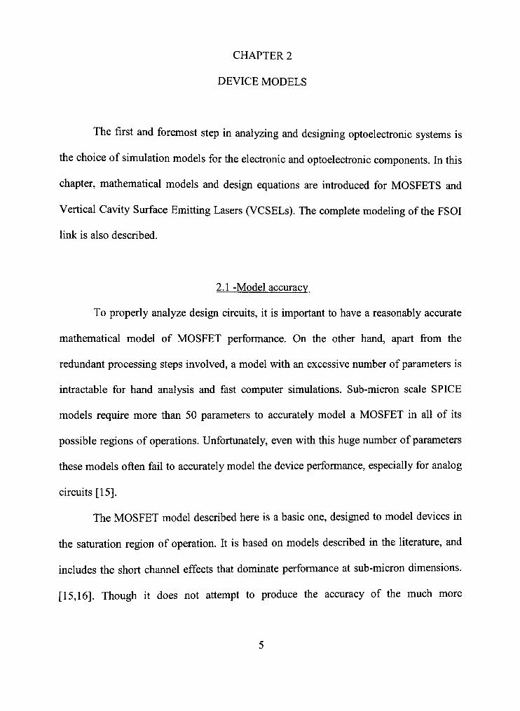
2.1.1 -CMOS device Model
High frequency MOS circuits typically employ short transistor gate lengths and
large gate-source voltages, since this combination produces the highest frequency (ft)
fransistors. To accurately model MOS transistors in this regime, short channel effects
must be considered. In saturation, with drain to source voltage being equal to gate to
source voltage (Vds = Vgs), the drain curtent per unit width (Idsatw) of the minimum length
device is given by [16,17]:
Idsatw =P ^^""^'^ ' (2.1) '^2[\+e((v^-v)]
Here, P is a proportionality constant determined for L=Lmin, Vgs is the gate-source
voltage, Vt is the threshold voltage, and the 0 term contains the short-channel effects of
both the gate (normal) electric field and the velocity saturation due to the source-drain
(tangential) electric field, and the source resistance.
The transconductance per unit width, gmw can be determined from the derivation
of Equation 2.1 with respect to Vgs:
^ 2 e ^ gmw t| dsatw
(V,s-V) l + 0(Vss-V,) (2.2)

The output conductance per unit width, gdsw, can be calculated from the process
Early voltage Vg and the coefficient r\ of the threshold voltage shift due to drain induced
barrier lowering (DIBL), by [16,17,18]
gdsw tdsatw 1 n (2.3) Ve (Vgs-V,)^
However, in short-channel devices, the dominant effect is DIBL. Thus, the output
conductance can be approximated by:
gd: sw -Misatw (2.4) (Vs^-VtY
where a fitting parameter m has been introduced to account for surface roughness
and other effects that reduce the output conductance at high bias voltages.
The small signal transistor model in figure 2.1 shows the model components.
Vgs Cgo
Figure 2.1: Small-signal fransistor model
From the above equations, we notice that the small-signal parameters gmw and gdsw
are both linearly dependent on the bias current Idsatw. The intrinsic gain of the fransistor,
which is the ratio of these two parameters,
Av = _ g" (2.5)
gdsw
is therefore independent of the bias current. It is, however, related to the bias voltage V gs-
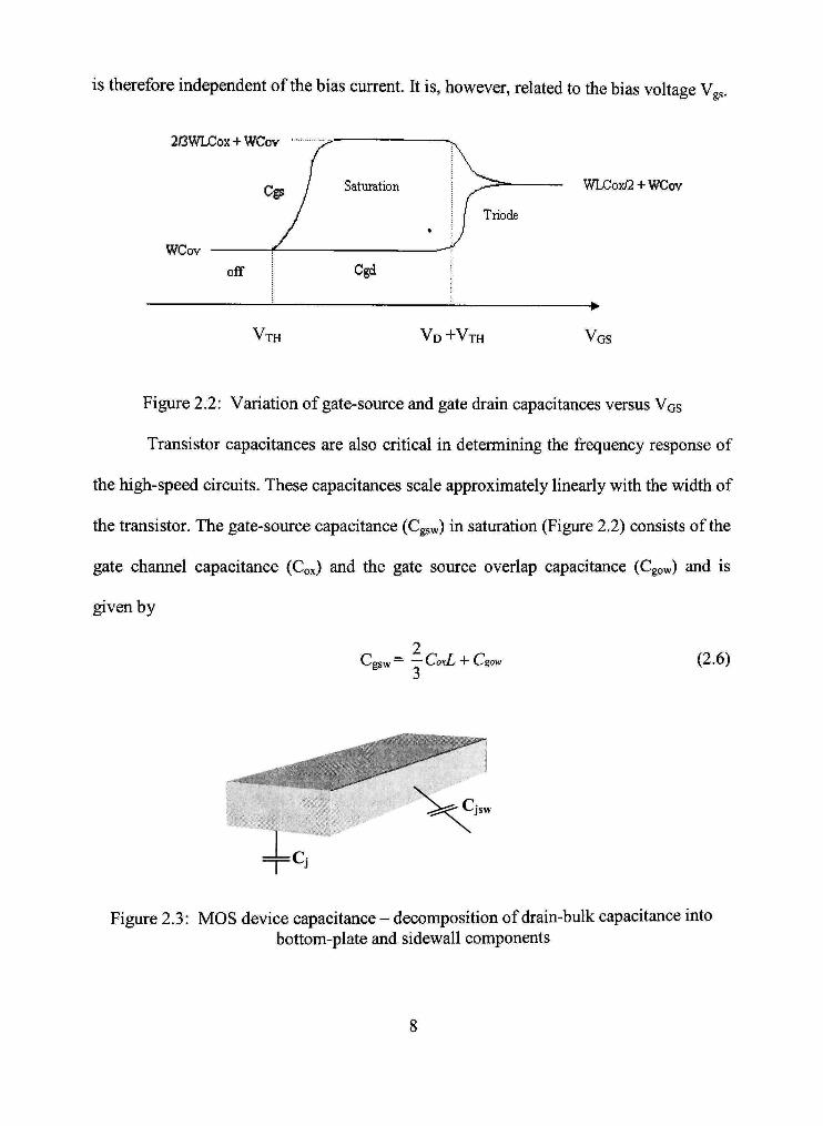
2/3WLC0X-I-WC0V
WCov
VTH
Saturation WLCox/2-t-WCov
VD +VTH VGS
Figure 2.2: Variation of gate-source and gate drain capacitances versus VGS
Transistor capacitances are also critical in determining the frequency response of
the high-speed circuits. These capacitances scale approximately linearly with the width of
the fransistor. The gate-source capacitance (Cgsw) in saturation (Figure 2.2) consists of the
gate channel capacitance (Cox) and the gate source overlap capacitance (Cgow) and is
given by
2 C gsw" • CoxLf + Cgow (2.6)
-il-.i^ .
=Cj
,^liZl
jsw
Figure 2.3: MOS device capacitance - decomposition of drain-bulk capacitance into bottom-plate and sidewall components

The gate-drain capacitance in saturation is determined solely by the gate drain
overiap capacitance, Cgow, and the drain-bulk capacitance (Figure 2.3) is given by the
junction capacitance of the bottom and sidewalls of the drain diffusion, Qw. The length of
the drain diffiision is assumed to be the minimum allowed by the process. Although the
junction capacitance is voltage dependent, in this case, constant worst-case values are
used for simplicity.
2.1.2 -Design parameters and exfraction
No matter how sound a physical model is, it cannot give results close to accuracy
unless appropriate values are used for the parameters. These should be chosen such that
the model predicts a behavior as close as possible to measurements.
Determining these parameters is not a simple matter, for several reasons. [18]
First, the value of some of these parameters may not be known accurately. Second, some
of the parameters in the model should be chosen for best matching to measurement,
(basically empirical in nature). Third, even if the value of a physical parameter is known
accurately, this value may not be the best one to use in the model expressions. This is
because analytical physical models are based on several assumptions and approximations;
using these expressions with the "cortect" values for this parameters results in certain
error. Because of all these difficulties, parameters from a pre-run 0.5 pm HP CMOS
BSIMl model from Mosis is taken as the model for this design. From the given model
various circuit design parameters are determined and they are listed in the Table [2.1]

Table 2.1: CMOS technology parameters
Parameter
Vdd(V)
Wmin (pm)
Cgow (fF/ pm)
Cgsw (fF/ pm)
Cjwn (fF/ pm)
Cjwp (fF/ pm)
Vtn(V)
Vtp(V)
0"(V-^)
0P(y-^)
mn
mp
Tin
Tip
Pn
pp ( pA ^
[y^pm^
0.5 ^m
3.3
1.0
0.3652
1.6631
0.43
0.91
0.556
0.72
0.189
0.116
4.41
4
.0243
.0273
185.3
48.3
10
The parameter values listed above in table [2.1] are obtained by using BSIMl
model equations. Most of these parameters are combination of other parameters and some
of them are empirical. Since BSIMl models are already available in PSPICE for
simulation, the accuracy of simulation results is limited by the accuracy of the supplied
BSIMl models.
2.1.3 -Parameter variations
As mentioned in Chapter 1, the loss of simulation accuracy when using a
fransistor model with only a few parameters is often inconsequential when designing in
digital CMOS processes. This is because the transistor parameter varies from wafer to
wafer, from die to die, and even from transistor to transistor. It is often difficult to predict
the accuracy or inaccuracy of the underlying transistor model.
There are two aspects of parameter variations in CMOS processing. One aspect of
parameter variation is the "lot-to-lot" variation, where all the parameters within a mn
have parameters, which vaty from the standard or nominal parameters. The limits on the
"lot-to-lof variations are defined by the process comers, and most foundries distribute
the transistor comer models along with the nominal model for simulation across the
process variations.
The other aspect of parameter variation is fransistor mismatch within a single
circuit. This mismatch is a smaller relative shift in fransistor parameters than the lot-to-lot
variations described above, but its effects can be more important because it limits the
ability to match identical devices in the same circuit.
11

2.1.3.1 Lot-to-lot variations
During design, lot-to-lot variations are taken into account through the use of
comer models, which predict the perfonnance of the NMOS and PMOS devices at the
exfremes of the process variations. There are basically four comer models normally
distributed with the typical device [19].
The "FAST" comer model is applicable when botii the NMOS and PMOS devices
are process biased towards faster-operation. The "SLOW" comer model is for the exact
opposite case of the previous model, both slow NMOS and PMOS devices, whereas
"UP" and "DOWN" comers are for slow NMOS and fast PMOS, or for fast NMOS and
slow PMOS, respectively
In a typical CMOS process, the variations of comer parameters from the typical
device parameters are seen to be large - on the order of ± 10%[ 16,20] for most of the
parameters.
2.1.3.2 Transistor mismatch
A widely accepted model for the mismatch of closely spaced, identical transistors
is presented in [20]. This model predicts the variance of the threshold voltage Vt and the
current factor p as a fimction of the gate width and length (W and L) of the devices, using
a normal distribution with zero mean.
The assumption in this analysis is that the mismatch generating process has
characteristics. First, the total mismatch is composed of many single mismatch events.
Second, the effect of each event is small, such that the contributions can be summed.
12

Third, tiie events have a con-elation distance much smaller than the transistor dimensions.
Mismatch generating processes which have these characteristics are for example, the
distiibution of implanted ions, local mobility fluctuations, oxide granularity and charg
etc[20].
According to this analysis, the variance is described as:
;es
o' (Vt) -
The current factor variance is given by
A VT
WL (2.7)
g- (P) _ A'p p^ W.L
(2.8)
The technology dependent constants Ayr and Ap are often difficult to obtain.
Kinget and Steyaert give a table of these constants for several different industiial
processes, which are reproduced here in Table 2.2 [21].
Table 2.2: Matching proportionality constants for different CMOS processes (from [21]).
Technology
2.5 pm
2.5 pm
1.2 pm
1.2 pm
0.35 pm
0.35 pm
Type
NMOS
PMOS
NMOS
PMOS
NMOS
PMOS
AvT
30 mV pm
35 mV pm
21 mV pm
25 mV pm
8 Mv pm
7 Mv pm
Ap
2.3
3.2
1.8
4.2
1.0
1.9
% pm
% pm
%pm
% pm
%pm
% pm
13
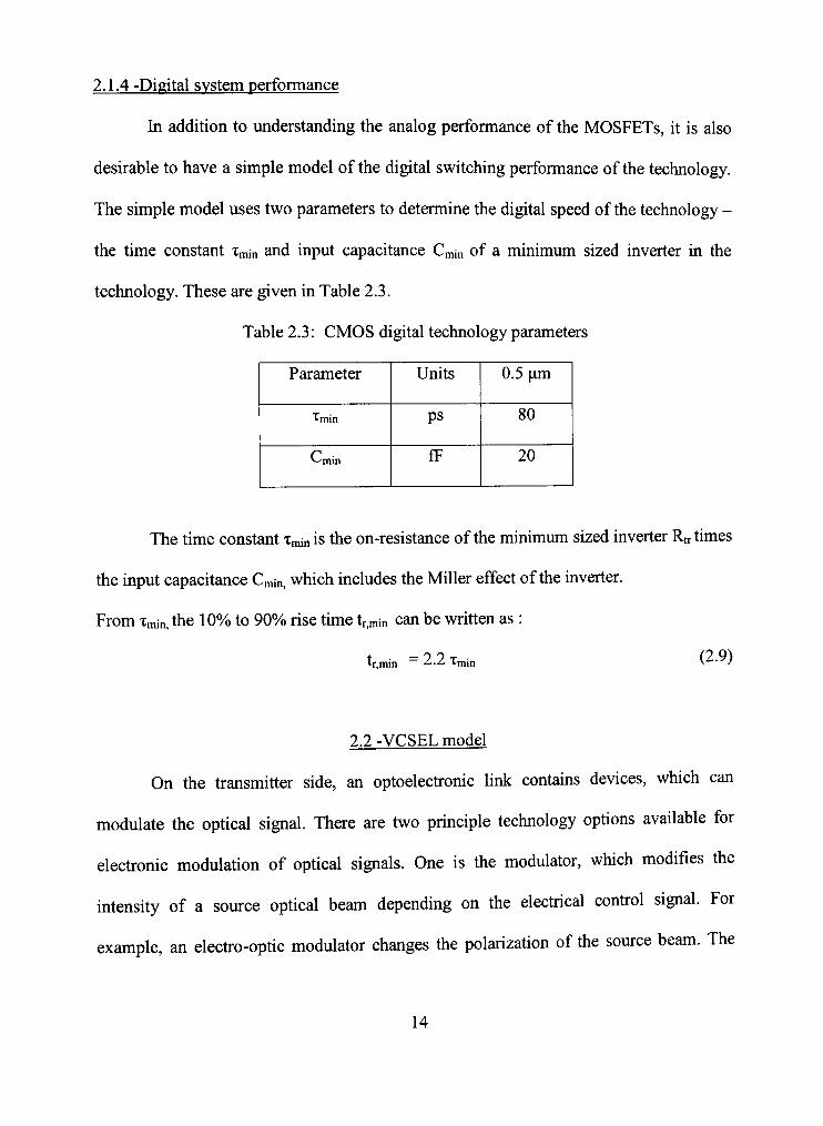
2.1.4 -Digital svstem performance
In addition to understanding the analog performance of the MOSFETs, it is also
desirable to have a simple model of the digital switching performance of the technology.
The simple model uses two parameters to determine the digital speed of the technology -
the time constant Xmin and input capacitance Cmin of a minimum sized inverter in the
technology. These are given in Table 2.3.
Table 2.3: CMOS digital technology parameters
Parameter
^min
^min
Units
ps
fF
0.5 pm
80
20
The time constant Xminis the on-resistance of the minimum sized inverter Rtr times
the input capackance Cmin, which includes the Miller effect of the inverter.
From Xmin, the 10% to 90% rise time tr,min can be written as :
tr,min = 2.2 Xmin (2-9)
2.2 -VCSEL model
On the transmitter side, an optoelecfronic link contains devices, which can
modulate the optical signal. There are two principle technology options available for
electronic modulation of optical signals. One is the modulator, which modifies the
intensity of a source optical beam depending on the electrical confrol signal. For
example, an electro-optic modulator changes the polarization of the source beam. The
14

polarization change is then mapped to an intensity change through the use of a
polarization filter. The otiier option is the emitter, which does not require a source beam
but instead produces the optical signal directly. VCSELs belong to the second type of
optoelecfronic device used for transmission.
A VCSEL is a semiconductor laser, in which light is emitted normal to the surface
compared to the other lasers in which light is emitted parallel to the surface. The forward
biased p-n junction provides the active medium. The cross-section of a typical VCSEL
device and that of an edge-emitting laser is shown in Figure 2.4.
/^^Z%—^^ < Jaserlight
player
active zooe
K ri4ayer
-active zone
n-)ayer
Figure 2.4: Cross-section of a VCSEL an Edge emitting device (from [22])
In VCSEL's unlike modulators the optical power is directly generated. Therefore,
the vertical cavity surface emitting lasers simplify the design of opto-elecfronic systems
compared to the modulating technologies.
The parameters used to model VCSEL performance in this study are the threshold
current and voltage (U and Vth), the electric current to optical power conversion
differential efficiency (r|Li), and the series resistance Rs. For the fastest operation, the
VCSEL is biased at or slightiy above the tiireshold current. When biased in tiiis fashion.
15

tiie intrinsic speed of modem VCSELs is quite high (greater than 4 GHz in [23]), such
that tiie output signal speed is determined by the CMOS driver and not the VCSEL
device (Table 2.4).
Table 2.4: VCSEL parameters used in this analysis, from [24, 25]
Type
Oxide - VCSEL
Implant-VCSEL
Ith
290 Ma
1.3 mA
11 Ll
0.7 W/A
0.42 W/A
Rs
250Q
85Q
V,h
2V
2V
Using these parameters, the average electrical power dissipation of the VCSEL
can be written as
Pelec= IthVth + ^ ( P ^ , + / ? , ( / „ + / J )
and the average optical power from the VCSEL is
p -IJlLI
(2.10)
(2.11)
where the VCSEL is biased at the threshold current for a zero output bit, and an
additional modulation current of magnittide Im is used to generate the one output bk. The
contrast ratio is assumed to be infinite in this model. Acttial operation would require
biasing the VCSEL above the threshold current, due to the variations across the artay and
temperattire effects. However, the modulation current is typically much larger than the
biasing current. This assumes an ideal biasing condition that does not greatly affect the
accuracy of the model.
16

A key design goal of semiconductor lasers is to confine the optical mode and the
injected carriers in the fransverse direction creating the laser aperture. The aperture has
been defined by different techniques with different VCSELs. One technology uses ion
implantation to define the aperture, the other uses oxide growth to do so. Oxide aperture
VCSEL in the literature have provided better confinement, and thus lower threshold
currents, but typically have higher series resistances. Table 2.4 gives the parameters for
the two types of VCSELs.
17

CHAPTER 3
RECEIVER CIRCUIT ANALYSIS AND DESIGN
3.1 Introduction
The previous chapter has reviewed the VCSEL transmitter model and how it can
be used to fransmit digital signals as laser light pulses. VCSELs are optoelectronic
devices that produce intensity modulated light beam based on the encoded digital signal.
However, the detection process is inherentiy analog, producing a current proportional to
the detected light intensity. A receiver circuit is required to convert this photocurrent to a
proper digital voltage level, which can then be used by the digital logic that follows.
To a large extent, the performance of a free-space optical intercormection depends
on the characteristics of the receiver. The four principle receiver characteristics are
sensitivity, bandwidth, power consumption, and area requirement. With appropriate
circuit and device design choices, these four characteristics can be traded off against each
other. More importantly, if one or more characteristics are fixed by the requirements of
the overall system, the others can be optimized. For example, the speed of the digital
circuitry that follows the receiver may be much slower that the fastest possible receiver.
By designing a slow receiver with better sensitivity and/or power dissipation overall
system performance can be improved. In a highly parallel and complex system, even
small improvements in the receiver can quickly add up to large improvements in the
overall system.
18

This chapter describes a framework for analyzing and modeling transimpedance
receivers for digital CMOS technology. First, the choice of appropriate receiver gain
stage, which is the basic building block of the receiver, is discussed. The transimpedance
amplifier, voltage amplifier, decision circuit are then described. Equations for the bit rate,
fransimpedance gain, noise, power dissipation and area of the receivers are introduced.
Then the method used to optimize receiver performance is presented. Finally, in chapter
4, the results of optimizing receivers and their simulation are produced.
One particular issue that is worth noting is that of the noise and bit error rate
(BER). The conventional receiver analysis concenfrates on noise source internal to the
receiver circuit i.e. thermal noise in the transistor channels, and dark noise from the
detector. On the other hand, standard digital CMOS design dictates so called "noise
margins" that principally account for extemal noise sources, i.e., switching noise on
power supply rails, and the cross talk through the substrate and from crossing
interconnects. In this chapter, the minimum optical power that provides the required noise
margin is compared with the thermal noise limited optical power required for operating at
a given bit rate. One result of the analysis is tiiat even at modest bit rates, the minimum
optical power required is determined by tiie gain-bandwidth product of the receiver and
the noise margin required in the logic circuks that follow the receiver, and not the intemal
noise source of the receiver. Such a resuh has been noted by Govindarajan [26], where
tiie sensitivity of the receiver is not determined by the noise sources but by the signal
swing required by the following digital circuit.
19

3.2 Previous work in optical receivers
Previous work in optical receiver analysis has concentrated on the noise
performance of the detector and receiver circuit. Personick's paper [27] is often cited as
the standard paper for designing receiver circuits for optical interconnect. Morikuni's
paper [28] expanded the analysis to account for more realistic transfer functions.
Williams [29] gives a noise equation, which includes the thermal noise of the following
stages of the receiver. A detailed analysis of the noise can also be found in [30]
3.2.1 Optimization
Several papers have discussed receiver optimization, and most reported designs
attempt some degree of optimization. From the noise analysis in Smith and Personick's
paper [31] the optimum pre-amplifier input transistor size that minimizes the thermal
noise can be calculated. Abidi's paper gives an expanded analysis of finding optimum
FET gate size where he finds that smaller gate widths than those given in [32] can be
used without excessively compromising the receiver sensitivity. Receivers based on
GaAs MESFETs have been described in [33] and optimized receiver gate widths were
slightly larger than those predicted by simple noise analysis.
Minasian [34] describes the optimization of a 4 Gbit/s MESFET receiver based on
minimizing the noise while simultaneously ensuring a phase margin of 77°. Das [35]
presents a optimization for receiver based on HBTs and MODFETs that produce a
maximally flat response (i.e. phase margin of 65°). However, both [35] and [34] use the
Personick analysis, which assumes raised cosine output pulses. As pointed out by
20

Morikuni [28], it is incorrect to use the Personick analysis for receivers that are not
individually equalized to produce raised-cosine pulses at evety bit-rate considered.
The paper by Kim and Das [36] uses SPICE simulations to determine bit-rate and
sensitivity limits of optimized HBT based receivers, hi their analysis, the feedback
resistance is kept constant and the feedback capacitance is varied to control the noise (and
signal) bandwidth. The fradeoff between the amount of intersymbol interference (for
small bandwidths) and the thermal noise (for large bandwidths) leads to an optimized
bandwidth for a given bit-rate. However, their fixed feedback resistance was chosen to
make the receiver maxknally flat at one "preferred" value of feedback capacitance. By
then varying the feedback capacitance, the receiver transfer function changes and reduces
the phase margin. This seems to negate the advantage of fixing the feedback resistance
for maximally-flat response.
An optimization for possibly the simplest receiver, a low-impedance front end
followed by a single CMOS inverter, is found in [37]. However, this receiver has poor
sensitivity and is difficult to bias. The three-stage transimpedance CMOS receiver
published by Ingles [38] is unique in that it was not optimized for noise performance but
for the largest amplifier voltage gain.
3.3 Receiver circuit design
Optical receivers can be classified as high-impedance, fransimpedance, and low
impedance depending on the pre-amplifier design. When the timing of the optical signal
21

is known, an integrate-and-dump pre-amplifier design can be used as well. The four
receiver configurations are shown in Figure 3.1.
4-' ^ A y ^ \ ^
Low R > Pre-amp High R Pre-amp
(a) (c)
reset dump
comp
Pre-amp
(b) (d)
Figure 3.1: Receiver classifications: (a) low impedance, (b) transimpedance, (c) high impedance, and (d) integrate-and-dump.
Low-impedance receivers have a broad bandwidth, but poor sensitivity. High
impedance receivers have much better sensitivity, but they fail to achieve a useful
bandwidth. The transimpedance receiver, which uses negative feedback to broaden the
bandwidth while maintaining a reasonable sensitivity, provides a good compromise
between the two extremes. In addition, the use of feedback self biases the pre-amplifier to
22

the high gain region of operation. The integrate-and-dump pre-amplifier can potentially
provide much better sensitivity tiian all of the other pre-amplifiers. It does this by
integrating the photocun-ent on a capacitor over the entire bit-period, instead of directly
converting the photocurrent to a voltage. A comparator can then be used to decide if the
integrator charge represents a one or zero bit. This is the principle of operation for the
clocked sense amplifier based receivers discussed by Woodward [39]. ft has also been
applied to electrical interconnects by Sidiropoulos and Horowitz [40]. However, these
receivers must be reset every bit, thus requiring either rettim to zero signaling as in [39],
or two interleaved pre-amplifiers as in [40]. hi addition, precise timing information must
be available to determine the integration period. These receivers are an area of continuing
research. Of all the receivers seen above, a transimpedance amplifier appears to be the
best option for pre-amplifier design. This chapter assumes a fransimpedance receiver
design.
Digital Output
Transimp.. • ^ ^ Amplifier
Voltage Amplifier
Decision Circuit
Clock
Figure 3.2: Transimpedance receiver block diagram
The operational model of a transimpedance receiver can be broken into different
components, as shown in Figure 3.2 - the fransimpedance amplifier (TIA), the voltage
amplifier and the decision circuit. The fransimpedance amplifier converts the
photocurrent from the detector to an analog voltage. This voltage is then amplified by the
23

voltage amplifier to match the requirements of the decision circuit. The decision circuit
provides a digital voltage output to the following digital circuits, which may be a digital
buffer and latch circuit, which synchronizes the output to the local system clock. A
current bias at the detector is used to provide an offset to detector current. This is done so
that the amplifier swings around the bias point, which is set by the self biasing action of
the fransimpedance amplifier to the point in the transfer curve where Vin = Vout.
(Figure 3.3). The current bias can be further increased to compensate for a non-zero
extinction ratio (i.e. optical power is present when transmitting a zero).
Vr ' A ' out Vr--- ^ 'out
Bias Point Bias Point
Vin Vm
Figure 3.3: Effect of the current bias on amplifier vohage swing (thick arrow): Without current bias and (b) With current bias
In this analysis no coding of the signal is assumed. Without a DC balanced code,
the receiver components must be DC coupled, and the decision threshold cannot be
derived from the signal but must be generated intemally. DC coupling also implies that
the DC bias conditions must be the same for all the amplifying stages, hi addition,
because of the large size and performance-limking parasitics of on-chip inductors, tiiis
analysis does not include designs with inductive peaking. A separate optimization of
inductive peaking in optical receivers is described in [41].
24
3.3.1 Gain stage
A fransimpedance receiver can include many amplifying stages, in both tiie TIA
and the voltage amplifier. A fiindamental issue in designing a receiver is the choice of the
gain stage circuit design. Since the stages are DC coupled, the bias points must be the
same for all the stages. This ensures that the entire amplification chain will be biased in
the high gain region. For this reason, the receivers are all chosen to be identical in this
study.
3.3.1.1 Gain stage options
Basic gain stage designs are depicted in Figure 3.4. A detailed analysis of these
gain stages can be found in standard textbooks on analog design [42,16], and is
summarized here. The amplifiers are assumed to be biased at Vin = Vout- The simplest
possible design is a CMOS inverter (Figure 3.4.a), which requires no bias voltage and
only two fransistors. This gain stage has the highest gain bandwidth product when driven
by a ideal voltage source, but this is partially offset by the large input capacitance due to
the PMOSFET when driven from a high impedance source. The gain is not very
adjustable by the designer, as the bias current cancels out to first order in the gain
equation. In addition, the gain is sensitive to process variations, as it depends on both the
NMOS and PMOS parameters. Another problem is that the gain falls off rapidly around
the bias point, limiting the valid region of small signal analysis. The stage also swings
from rail to rail, which is of course one reason it is preferred for digital circuits. For a
receiver, however, a gain stage with a large output swing can reduce the dynamic range
25
by slowing down the receiver when it is operated with a larger optical power than the
minimum required optical power. This is due to the limited slew rate of the amplifier
when it is operated beyond the small signal limits.
The next simplest is the cmrent source inverter (Figure 3.4.b), which replaces the
signal voltage on the PMOSFET with a constant bias voltage. This stage can have a lower
input capacitance than tiie CMOS inverter, but since the transconductance of the
PMOSFET is not used it also has a smaller gain. However, the bias voltage gives more
freedom to adjust the gain of the stage, which can be tuned over a relatively wider range
than that of the CMOS inverter. In addition, with proper biasing the power supply
rejection ratio of this gain stage can be improved over that of the CMOS inverter. Both of
these designers suffer from the Miller effect, which multiplies the parasitic capacitance
between the gain and drain of the input MOSFET by the gain.
This effect is avoided when using a cascode design (Figure 3.4.c & 3.4.d). The
cascode transistor, which is basically a common gate amplifier, also greatly increases the
gain at the expense of the bandwidth. However, the gain in this case cannot be
determined accurately, as the inaccuracies in the modeled output conductance are
effectively squared by cascode action. In addition, the parasitic capacitance of the
additional transistor lowers the gain-band width of these amplifiers to below that of the
non-cascode amplifiers. Other disadvantages are multiple bias voltage are required, and
poor perfonnance at smaller power supply voltages due to the exfra voltage drop required
across the cascode fransistor.
26

The gain stage design used in our analysis is the ratioed current source inverter
and is shown in Figure 3.4.e. This gain stage is based on the current-source inverter
(FETs Ml and M2), but includes an additional diode connected transistor (M3) at the
output. M3 serves to shift the output pole to higher frequencies, by reducing the small
signal impedance on the inverter's output node; it also simultaneously reduces the gain of
the inverter. This allows more precise control over the gain and the bandwidth of the
stage, which is critical in determining the receiver's fransfer function. The maximum
output swing of the RCS inverter is reduced from that of the other inverters.
Vin
,hJ _M2
Vout
jyyti
h o—\li^ Vb
Vin
Vout
J
Vbl
, ^ O 1 N»
Vb2
K3
i_J Vout
o 1-*^ M2
U a ^ 1 - *
Vin Ml
J
(a) (b) (c)
Figure 3 4- Gain stage circuit design: (a) CMOS inverter, (b) current-source inverter, (c) telescopic cascode, (d) folded cascode, (e) ratioed current -source inverter
27

Vin 0—
h Vbl J o- \Ui-^
M-*-
J
Vb3 0 —
Iwll M. L-!, Vb2 -*^\ 0
Vout
m
h Vb J 0 — \ l ^ ^
Vin 0— Ml
J
M3 J
li
Vout
(d)
Figure 3.4: Continued
(e)
3.3.1.2 R C S inverter design
The analysis of the RCS inverter is important in determining the gain and
bandwidth of the receiver circuit. Referring to Figure 3.4 (e), the output voltage and the
input voltage are the same when biased in the high gain region, Vin = Vout = Vgs. The bias
voltage Vb on M 2 is chosen to be the same as drain voltage, to ensure that it remains in
saturation. The gain of the corresponding current source inverter is given by
Ao = gml
(3.1) gds\ + gikl
It can be seen that the gain depends on the gate source voltage of Ml. Changing
the value of WI changes the bias current but does not alter tiie gain much. But when the
effect of M3 is taken into account, the fransconductance of M3 adds to the output
conductances in the denominator of Equation 3.1. This means the ratio of Wl to W3
28

becomes important. Small values of this ratio cortespond to low gain, high-speed
amplifiers, whereas larger values conespond to higher gain, lower speed amplifiers. The
gain with M3 is given by
Av = gmiRo = r (3.2)
where Ro is the output resistance given by
Ro= ^- (3.3) gdsi + gdsl + gdsl + gml
If this gain stage is the last or the only stage in the TIA, it has a feedback resistor
as its output. This feedback resistor lowers the gain of the amplifying stage in loads.
Taking into account the effect of the feedback resistor, the loaded gain is given by
Av = (3.4) Ro + Rf
The input and output capacitance of the amplifying stage can be written as
Lin,amp ~ ^-•gswW1 t.-'--'J
Cf.amp = CgowW, (3 .6)
Ci„,amp,,™Uer =[Cgsw + Cgow( 1 + A v ) ] W i (3 .7 )
Cout,amp = CjwWi+ (Cgow + Cjw )W2 + Cgsw+ Cjw)W3 (3 .8)
where the second term in equation 3.7 is due to the Miller effect. The width of M2
is given by equating the currents in the P and N devices, and is given by
W2 = Z(Wi+W3) (3-9)
where Z is given by
29

^ _ p«(Vgs - VnY [1+ep(Vdd - Vgs - Vtp)] pn(Vdd - Vgs - v,pf [1+a,(Vdd - Vm)] (3.10)
The pole at the output of the amplifying stage determines its 3-db bandwidth. This
pole can be written as
1 f -3db - (3 .11)
27tRo\Cout,amp-\-Cnext)
If this stage is loaded with the feedback resistor, it will act in parallel with the
output resistance, moving the pole to:
1 f -3db-f-3db+ (3.12)
2 TlRfxCout .amp+Cnexl)
Cnext in equation 3.12 is the input capacitance of the next amplifying stage,
Ci„,amp,niiiier, Or the input capacitancc of the decision circuk, Cdc, if this is the last stage in
the receiver. Thus, given the CMOS process parameters, the gain and bandwidtii of the
RCS inverter can be written in terms of Wi and Vgs.
h ,HJ
f * -UC
M3^J
u
Vb
Figure 3.5: Gain stage voltage bias generator
30
The gain stage voltage bias V^ can be generated from an additional gain stage by
tying its input and output together, as shown in Figure 3.5. If a lower output resistance is
required from the bias generator, several stages can be used.
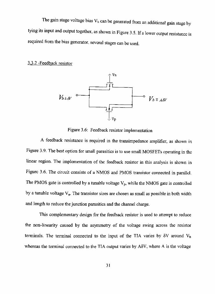
3.3.2 -Feedback resistor
•^ Vn
Vb ±SV
" i i r
VbT ASV
Vp
Figure 3.6: Feedback resistor implementation
A feedback resistance is required in the transimpedance amplifier, as shown in
Figure 3.9. The best option for small parasitics is to use small MOSFETs operating in the
linear region. The implementation of the feedback resistor in this analysis is shown in
Figure 3.6. The circuk consists of a NMOS and PMOS transistor connected in parallel.
The PMOS gate is controlled by a ttmable voltage Vp, while the NMOS gate is confrolled
by a tunable voltage Vn. The fransistor sizes are chosen as small as possible in both width
and length to reduce the junction parasitics and the channel charge.
This complementaty design for the feedback resistor is used to attempt to reduce
the non-linearity caused by the asymmetty of the voltage swing across the resistor
terminals. The terminal connected to the input of the TIA varies by 5V around Vb
whereas the terminal coimected to the TIA output varies by ASV, where A is the voltage
31
gain of the TIA. This means that the NMOS transistor will be ttimed on to a greater
extent when the output of the transimpedance amplifier is low versus when it is high. The
PMOS fransistor balances this trend by filming on when the fransimpedance amplifier
output is high.
3.3.3-Decision circuit
The decision circuit is chosen to be a current-source inverter (Figure 3.7) instead
of a RCS inverter. This is because a precise gain is not required in the decision circuit,
and the RCS inverter's limited voltage output swing is not appropriate for the decision
circuit, which must produce digital logic level outputs. The ratio of the PMOS to NMOS
width in the current source inverter is calculated to make the inverter switching voltage
the same as the bias vohage Vb. This ensures that both fransistors are in the saturation
region at the switching point. This ratio is given by the parameter Z defined in
equation 3.10.
32

ov
„lp
l]
Vb 1 1 —
0 IH'
^ Cload Vl^AV/2 ,
12
^ 1 1
^ Cload
Minimum size CMOS inverter Decision circuit
Figure 3.7: The decision circuit output rise time is made equal to that of a minimum sized CMOS inverter by setting the width of PMOS such that I2 - Ii = Ip
The operation of the decision circuit is non-linear, and a small signal analysis is
not applicable. A minimum voltage swing, AV, must be input to the decision circuit to
ensure an adequate output swing. This input voltage swing is the width of the voltage
fransition region of the decision circuit.
The width of the transition region for the decision circuit is given approximately
by AV~20%Vdd. As Vb increases the NMOS size decreases. This reduces the pull-down
ability of the NMOS device, thus allowing the low output level to rise. However, with the
given AV the output swing is at least 60% Vdd for all values of Vb.
The ratio of the PMOS to NMOS width is set by Vb,but the absolute values of the
widths are determined by the required switching speed. If larger widths are chosen, the
decision circuit will be able to switch its load capacitance quickly, but will present an
unacceptably large load to the receiver amplifier and thus slow it down. On the other
33

hand, if the devices are undersized, then the decision circuit becomes the speed limiting
circuit of the receiver. To analyze the affect of the decision circuit, its speed must be
characterized in terms of the transistor widths.
The decision circuit rise time is typically slower than its fall time, due to the
smaller pull-up sfrength of the PMOS transistor. In order to develop an equation for the
decision circuit rise time, we first find the condition where the rise time is equal to that of
a minimum sized CMOS inverter (with PMOS width Wp = 3Wmin and NMOS width
Wn== Wmin)- The initial charging currents when the input is switched from high to low are
set equal by an appropriate choice of W2:
l2-Ii = Ip (3.13)
where Ip is the initial charging current of the PMOS in the CMOS inverter (with
Vgs = Vdd), I2 is the charging current through M2 (Vgs,2 = Vdd - Vb), and Ii is the
discharging current through Mi (Vgs,i = Vb - AV/2). These curtents are shown in Figure
(3.7). The width of M2 (and thus of Mi through the factor Z) is chosen to solve the
equation (3.10)
The rise time of the decision circuit can thus be written in terms of the rise time of
a minimum sized CMOS inverter, as:
tr = 2.2Xn
ff Ip Y^^Cnex^^
\\l2 — I\ J\ Cminy (3.14)
Cmin is tiie input capackance of a minimum sized inverter and Xmin is the RC time
constant of a minimum sized inverter as given in section 2.1.4.
34

3.3.4 -Digital Buffer
The first stage of the digital buffer is a small CMOS Schmitt trigger. This is
followed by a cascade of CMOS inverters, starting with a minimum-sized inverter and
scaling upwards is size by a constant factor g (Figure 3.8). This super-buffer arrangement
presents a small load capacitance to the decision circuit, while the super-buffer output
drive capability can be increased by adding additional scaled stages.
The ratio of the input fransistor width to the feedback transistor width in the Schmitt
tiigger is chosen to give a hysteresis loop with a width Vhyst of approximately 20% Vdd-
This ratio is given by [43]
In
J \ ^ 6Witiin 3Wmin
H
h " 1 LIF
| [ 7 i PWmiti
h-l 3Wmin i-«t—1
u ^*- | 2Wnnm Wmin
• - | 3Wmin ' ~1 g(3Winin) n g2(3WKBn)
I I—, I h - i
H J
J
J
Wmin HEn
g(Wmin)
Out
g2(Wmin)
Schmitt Trigger Super-buffer
Figure 3.8: Digital buffer
35

Pr = \''^dd ''^hyst)
V dd + '^hysl ~^K J (3.15)
A minimum fransistor is chosen as the NMOS feedback transistor, and the two
NMOS input transistors are sized at 2 and 3 times the minimum width. The PMOS
fransistors are sized 3 times larger than the cortesponding NMOS transistor. Using the
fransistor widths shown in Figure 3.8, the input capacitance of the Schmitt trigger can be
written in terms of the input capacitance of a minimum sized inverter (Cmin)- The input
capacitance is approximately 5Cmin-
The Schmitt trigger circuit is included to suppress oscillations due to unintended
feedback from the super-buffer into the receiver amplifiers and decision circuit. By
adding this hysteresis to the digital buffer, the switching of the super-buffer does not
occur when the decision circuit is in its highest gain region of operation.
The final super-buffer stage drives the latch capacitance Ciatch. The number of
stages is chosen to minimize the propagation delay, while maintaining a fast enough edge
rate that the data input to the data latch is stable around the clock edge.
3.3.5-Data Latch
The last component of the receiver is the data latch. The latch samples the output
of the digital buffer at the rising edge of the system clock. The sampled value is stored
until the next rising edge. This allows the incoming data to be resynchronized to the local
clock. The clock edge is nominally aligned with the center of the receiver bit, although
jitter and skew in the clock and the data will cause the sampling point to move.
36

3.4 -Receiver Model
Using the analysis for the receiver building blocks from the previous section, the
fiill receiver can be developed. The transimpedance amplifier is designed for stability by
choosing an appropriate amount of feedback. The total transimpedance and the bit rate of
the receiver can be calculated, as well as the input equivalent noise, electiical power
dissipation, and the circuit size, given the receiver configuration. The receiver is coded as
1+P, where 1 is the number of stages in the transimpedance amplifier, and P is the
number of stages in the voltage amplifier.
3.4.1 -Transimpedance amplifier
The fransimpedance amplifier (TIA) converts an input current to an output
voltage. A feedback resistor Rf determines the fransimpedance and thus the sensitivity of
the amplifier. Larger feedback resistors increase the sensitivity of the amplifier, but
simultaneously reduce the amplifier bandwidth. The bandwidth of the amplification
stages that make up the TIA limit the ultimate speed of the TIA.
MiHR
1 - Stage TIA
Figure 3.9: Circuit for one-stage fransimpedance amplifier
37
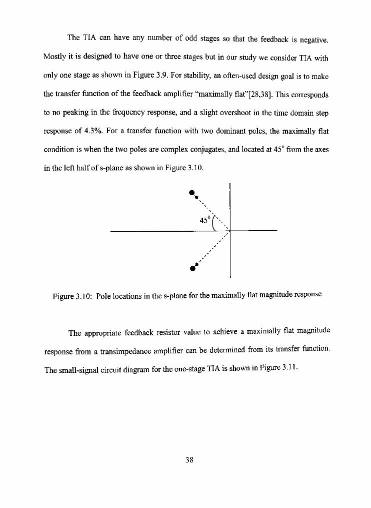
The TIA can have any number of odd stages so that the feedback is negative.
Mostly it is designed to have one or three stages but in our study we consider TIA with
only one stage as shown in Figure 3.9. For stability, an often-used design goal is to make
the fransfer function of the feedback amplifier "maximally flaf [28,38]. This corresponds
to no peaking in the frequency response, and a slight overshoot in the time domain step
response of 4.3%. For a fransfer function with two dominant poles, the maximally flat
condition is when the two poles are complex conjugates, and located at 45° from the axes
in the left half of s-plane as shown in Figure 3.10.
n\
Figure 3.10: Pole locations in the s-plane for tiie maximally flat magnittide response
The appropriate feedback resistor value to achieve a maximally flat magnittide
response from a transimpedance amplifier can be determined from its fransfer fimction.
The small-signal circuk diagram for the one-stage TIA is shown in Figure 3.11.
38

Rf
Cf
® lin t gmVir Ro
Vout
=F Cout
Figure 3.11: Small signal circuit for the one-stage fransimpedance amplifier
The corresponding transfer fimction can be written as [28].
A + sB ZT(S)
C + sD + s^E (3.16)
where the constants are:
A = Ro-AvRf (3.17)
B^RoRfCf (3.18)
C = l + A v (3.19)
D = Ro (Cin + Cout) + Rf (Cf + Cin) +RoRfCf (3.20)
E - RoRf [(Cin + Cout) Cf + CinCout] (3-21)
and Av = gmRo is the unloaded gain of the one stage amplifier
Note that in this section Cin is the input capacitance to ground of tiie amplifier and
the photodiode capacitance, Cout is the total output capacitance to the ground of the
amplifier plus the capacitive load of the next stage, and Cf is simply the amplifier
feedback.
39
Cin = Cpd + Cin,amp (3 .22)
Lout ~ Cout,amp+Cnext (3 .23)
Cf = Cf,amp (3 .24)
When the parameters of the gain stage are known, the location of the poles of the
fransfer fimction (Equation 3.16) can be plotted as a fimction of the feedback resistor
value. For large feedback resistances, the two poles are both on the real axis, and
separated such that the pole at the input is cleariy the dominant pole. As the feedback
resistant reduces, the poles move towards each other until they merge. Then they become
complex conjugates, and move away from the real axis in opposite directions. They also
move towards the left due to the broadening effect of the decreasing feedback resistance.
As shown in Figure 3.12, the intersection of the root locus plot with the 45° angle
line marks the maximally flat pole positions. These points indicate the value of feedback
resistances that produces a maximally flat fransfer function. Now we need to find an
expression that helps to find out the feedback resistances value.
40

hnag(s)
Real(s)
Figure 3.12: Pole locus for one-stage transimpedance amplifier as the value of Rf is changed
Analytically, the maximally flat response of equation 3.16 occurs when:
D^ = 2EC (3.25)
Solving equation 3.25 leads to the following quadratic equation in Rf
Rf2[Cm+ ( A v + l ) C f ] 2 + Rf [ 2RoCin(Cin - AvCout)] + [R0^(C,n+ Cout)'] = 0 (3 .26)
For convenience and ease of solving the above equation, we take the ratio of two
capacitance as
x = •^out (3.27)
y = ^ -C .
Rf = ff
[i+(4,+i)>^j - [^x- l±V(4+l ) [ (4-V-2x-(x + l) (2>' + (4+l)}^)]
(3.28)
(3.29)
41

The two poles are located at Pi,2 = -a ± ia.
Where a = — (3.30)
2 If we assume y -0 , Av » 1 and x » - - , then the solution can be simplified as
Rf=2AvXRo (3.31)
This simplified solution can be written in terms of the open loop poles of the TIA
as
Pout=2AvPin (3.32)
i.e., the open loop poles are separated by the factor of twice the gain. This is often
cited criteria in receiver design papers as in [38]
The simplified solution can lead to significant errors when the gain is not large, as
is the case with the receiver studied here. For this reason, equation 3.29 is used in this
analysis for the one-stage TIA.
The transimpedance of the one-stage TIA is given by
Zf = ^Lllll. (3.33) 1 + ^"'
and the 10% - 90 % rise time of the one-stage TIA, when tiie fransfer fimction is
maximally flat, is
^^_ 2.2V2 (3 34)
2a
42

3.4.2 -Voltage Amplifier
The voltage amplifier consists of a cascaded series of amplifying stages. As
mentioned previously, the stages are all identical and use the same design as the stage in
the fransimpedance amplifier, to ensure proper DC biasing. The total gain provided by
the p-stage cascaded voltage amplifier is thus Av , where Av is the gain of the single stage
as defined in section 3.2.1.
One important consideration in the voltage amplifier is the effect of parameter
variations on the DC biasing. Small variations in the transistor parameters can cause
offsets that are amplified by subsequent stages in the amplifier, such that later stages may
no longer be biased correctly. This problem is alleviated somewhat by the use of
feedback in the TIA, but it must be taken into account in the voltage amplifier. Typical
offsets between identical transistors in modem CMOS process are in the lOmV range.
Since the gain of the amplifying stages is typically between 3 and 5, the maximum
number of stages in the voltage amplifier is limited to two to keep the offset at the output
of the voltage amplifier below 250mV. This ensures that all stages are cortectiy biased
and that the input to the decision circuit swings about the threshold point. Although the
offset improves slightly for smaller line-length technologies, the voltage swing reduces as
well, indicating that the two-stage limit is reasonable choice for the case under sttidy.
The pole at the output of the amplifying stage is at Pout = • Putting this in ^out^oul
tenns of a used above for the fransimpedance amplifier poles means Pout = 2a for one-
stage TIA.
43

Thus the 10%-90% rise time of each stage in the voltage amplifier is:
. 2.2 ' ' - ^ (3.35)
3.4.3 -Bk Rate
The speed of the receiver amplifier acting in cascade can be written in terms of
the minimum signal rise time at the input to the decision circuit. This can be found by
adding the square of the rise times of each amplifier and taking the square root of the
sum:
k^mps-^jtfju+P^ (3-36)
where p is the number of the vohage amplifiers used in the receiver. Writing this
in terms of a gives:
t = : ^ (3.37) ••r.amps ^ '
a
where X is given for different receiver configurations.
44
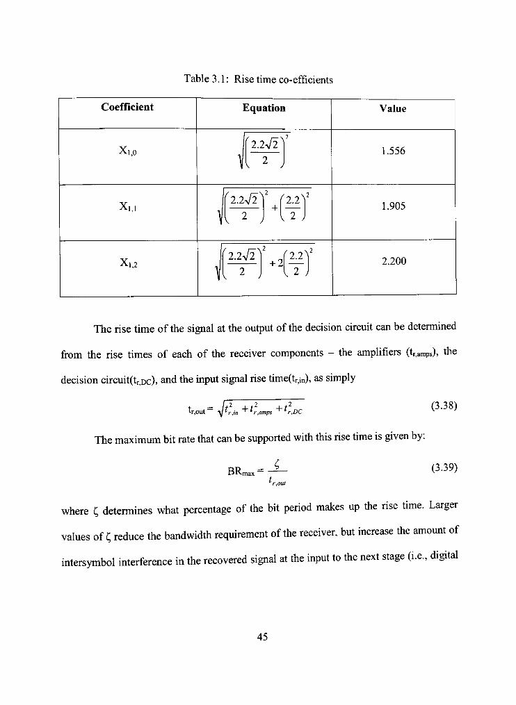
Table 3.1: Rise time co-efficients
Coefficient Equation Value
X 1,0 ^2.2V2V
1.556
X 1,1 2.2^2^ ("2.2
+ V
1.905
X 1,2 '2.2V2'
I 2 J
2
+ 2 I 2 J 2.200
The rise time of the signal at the output of the decision circuit can be determined
from the rise times of each of the receiver components - the amplifiers (tr,amps), the
decision circuit(tr,Dc), and the input signal rise time(tr,in), as simply
t = [?~7? +t^ (3-38)
The maximum bk rate that can be supported with this rise time is given by:
^ (3.39) BRmax ~ r,out
where C detennines what percentage of the bk period makes up the rise time. Larger
values of C reduce the bandwidtii requirement of the receiver, but increase the amount of
intersymbol interference in the recovered signal at the input to the next stage (i.e., digital
45

buffer). In a synchronous receiver, C can be taken to be about 60% without significant
signal degradation [44].
3.4.4 -Transimpedance Gain
The overall fransimpedance gain, TZ is the receiver's output voltage divided by
the input current, and is given by the voltage gain of the p-stage post amplifier times the
fransimpedance of the TIA:
TZ = A'^Z^ (3.40)
For a receiver to operate correctly, a minimum average optical input power is
necessaty. This is the optical power that results in a voltage swing AV to the decision
circuit. Dividing AV by the transimpedance of the receiver, TZ, yields the required signal
current.
• TZ
Dividing is by the responsivity of the detector, Rpd yields the average optical
power:
p = ' (3.42) '" 2R,
where the factor of two accounts for the assumption tiiat half of the bits are on and
half are off
The value of AV for the decision circuks used here is Vdd/5. The required average
optical power is then:
46
p = dd
lOR^JZ (3.43)
3.4.5 -Power
The electiical power dissipation of the (l+P)-stage receiver is determined from
the gain stage bias current, lb, and the power supply voltage, Vdd, and can be written
Pd=[(^ + P)h+IdcVdd (3.44)
where Idc is the decision circuit bias current.
There is additional power dissipation due to the switching of the node
capacitances in the receiver, but this component in orders of magnitude less than the
power dissipation due to the bias current. This is because the signal swings and the
capacitances involved are small.
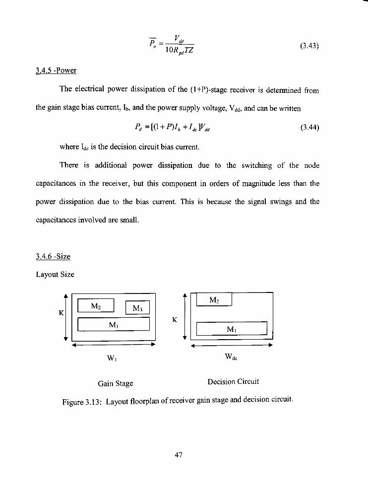
3.4.6 -Size
Layout Size
K
Wi
ii
M2 M3
Ml K
ik M2
Ml
Wdc
Gain Stage Decision Circuit
Figure 3.13: Layout floorplan of receiver gain stage and decision circuit.
47
The total circuit area of a receiver with (l+P)-stages and a decision circuit with
NMOS fransistor with of Wdc can be approximated by
Area = (l+P)KWi + KWdc (3.45)
where K is the layout height determined by the technology and it is taken as a
constant. However, the physical circuit area may not be the limiting factor in determining
the density of receivers. With high power dissipation of these receivers, the thermal
power density must be considered. In this case, with a maximum power density of Pmax
dictated by the cooling method, the effective size of the receiver is
A r e a = ^ (3.46) P
max
So, for example, a receiver that dissipates ImW of power on a chip that has a
maximum power dissipation of lOW/cm requires 10,000pm .
3.5 -Noise
The circuit noise introduced by the receiver and detector is referted to the receiver
input for signal to noise ratio detennination. Since the circuit noise usually dominates the
optical signal shot-noise, it determines the maximum obtainable signal to noise ratio. The
circuit noise consists of several components. The first component is the shot-noise of the
leakage(dark) cun-ent of the detector. The second component is the thennal noise due to
the feedback resistor. The third component is the thennal noise due to the gain-stage
transistors. We examine each of these noise sources in ttim. The noise sources are shown
in Figure 3.14.
48

Figure 3.14: Noise sources in the receiver
The current noise spectral density of the shot noise due to dark current of the
detector is given by
Sdark(/) = 2qldark (3-47)
where it is seen that this noise is white and acts at the input of the receiver.
The thermal noise due to the feedback resistor can be approximated as a current
noise source at the input of the receiver with spectral density
4KT Srf(/) =
R, (3.48)
where the approximation assumes tiiat the forward current-gain through the
amplifier is greater than that through the feedback resistor[30]. This assumption is easily
met for any non-trivial design. This noise is also white.
The thermal noise in the gain stage itself is due to the channel resistance, and
appears at the output of the gain stage as a noise curtent spectral density of
Sga.n(/) = 4 K T r ( Z g J (3-49)
where Sg„ is shorthand for gmi + gm2 + gm3-
49
This noise can be referred to the input of the gain stage by dividing by the
magnittide squared short-circuit current gain of the stage. Then, by dividing by the
magnittide squared short-circuit current gains of the preceding stages, the noise at any
gain stage can be refen-ed back to an input equivalent noise spectral density as described
in [30].
Thus, to complete the analysis, the short-circuit current gains must be determined.
This will be done for the fransimpedance amplifier and the voltage amplifier separately.
R.
(1 -^v)
gmVi
rj: CI
R,
(1- ,
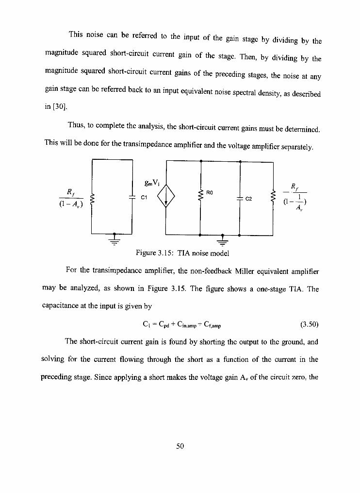
Figure 3.15: TIA noise model
For the fransimpedance amplifier, the non-feedback Miller equivalent amplifier
may be analyzed, as shown in Figure 3.15. The figure shows a one-stage TIA. The
capacitance at the input is given by
'-'1 ~ ^ p d + »-'in,amp + ^f.amp ( j . j U j
The short-circuit current gain is found by shorting the output to the ground, and
solving for the curtent flowing through the short as a function of the current in the
preceding stage. Since applying a short makes the voltage gain Av of the circuit zero, the
50
input referted feedback resistance R.
\-A.. and the output referted feedback resistance
R, becomes simply Rf The short circuit curtent gain can now be found.
1 A.
a i -Sn,lR ml^^J
l + sRfC^
where ai is the short-circuit current gain of the single stage TIA.
(3.51)
Vi Rf
I V * A -
T CI g"''Rrg V am 0 om I
Vb
gmVa
Vn
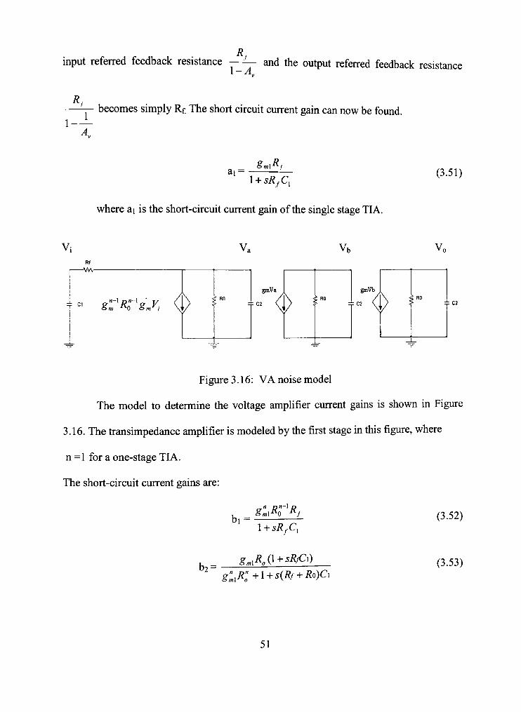
Figure 3.16: VA noise model
The model to determine the voltage amplifier current gains is shown in Figure
3.16. The fransimpedance amplifier is modeled by the first stage in this figure, where
n =1 for a one-stage TIA.
The short-circuit current gains are:
b ,= l + sRfC,
b2 = g„,RA\ + sRjC^)
^:,^:+i+^(^/+^°)<^>
(3.52)
(3.53)
51

, ^ gm\Ro ' Ur^^2 (3.54)
b, is the short-circuk curtent gain of the first (transimpedance) stage, bz is the short-
circuit curtent gain of the first voltage amplifier stage, and h is the short-circuit current
gain of the following voltage amplifier stages.
The total input equivalent noise current spectral density can now be written
Si ( / ) - 5,„,, ( / ) + Sr^ ( / ) + 5„, ( / ) + S,, ( / ) (3.55)
where tiie noise due to the fransimpedance amplifier is
STIA (f) - Sgain (f) - + • - + • 1 |2 ' I | 2 | |2 • I | 2 | | 2 | |2
ai \m\ lail \a\\ a: lail (3.56)
The noise due to the voltage amplifier is
SvA (f) - Sgain (f) k l ^ l L |2 | L | 2 | , | 2 | , |2 \b\\ 02 \bl\ \bl\ 03
(3.57)
in This equation is for two vohage amplifier stages - for one stage, the last term i
the equation is dropped. For no voltage amplifier stages, SvA(f) = 0.
To reduce the complexity of the total noise equation, we keep only the dc terms
and terms with the input pole, RfCi. The higher order poles are ignored, because their
effect is negligible after the integration over the receiver fransfer function. We also
assume that the feedback resistance is large enough so that Rf » Ro and the gain gmiRo
is written as Av. The total input equivalent noise curtent spectral density is then given by:
4KT T^" Si(f)= 2qLark+^^^^+4KTr^
^ SnA
( 2 (n-\
\Rf Vn=0 j = 0
n+p-I
i;4-"+Z4-"V(2^G)^£4--Is
j = 0
(3.58)
52

where n + p is the number of gain stages in the receiver, n being the number of TIA
stages and p being the number of VA stages.
The total noise equation suggests that at different frequencies, the noise of the
voltage amplifier is treated differently. At high frequencies, where the term (2jifCi)^
dominates, the noise from the voltage amplifier is divided down by the voltage gain of
the fransimpedance amplifier stages - hence, the high frequency noise from the voltage
amplifier does not greatly contribute to the total noise. However, at low frequencies,
where the term —^ dominates, the noise from the voltage amplifier is not divided by the
gain of transimpedance amplifier stages. The low frequency noise of the first stage of the
voltage amplifier has just as much effect on the total noise as the low frequency noise of
the first stage of the fransimpedance amplifier. This difference between high and low
frequency noise is due to the changing impedance of the input capacitance Ci. At high
frequencies, the low impedance of Ci means most of the input current flows through Ci
instead of Rf. Thus, the effect of the feedback is reduced and the transimpedance
amplifier acts more like a cascaded series of gain stages.
When integrating over frequency, the dominant component of the total noise
equation is the high frequency term. This means the noise of the voltage amplifier is a
minor contributor to the total noise, as it is effectively divided by the gain of the
transimpedance amplifier stages. However, the difference between low frequency and
high frequency noise is important in the detennination of the supply rejection and the
effects of parametric variations.
53

The input equivalent curtent noise is found by integrating over frequency the total
input equivalent noise curtent spectral density multiplied by the squared nomialized
receiver fransfer function
( . ; > ^ , ( / ) | ^ / Zr(0)|
This can be written as
(!^) = 2qL.., + ^ + 4KTT^^^'" Rf (SmM
(n-\ p-\ \
X^;"+Z<" \n=0 i=0
Jn.
,amps
4KTri4^(27tfc^y"f^A;'' §m\ s=0
Kit. J
ramps
(3.59)
(3.60)
The value of Jn,p and Kn,p depend on the fransfer function of the receiver ZT(/), and
are given by
'}\Zr(af)\ Jn,p = Xn,p\- ;T-df
0 |Zr(0)|
0 |Zr(0)|'
(3.61)
(3.62)
From the fransfer fiinctions, the value of the integrals in equation (3.61) and
(3.62) can be determined for each receiver configuration. The values are given in Table
3.2 [31].
54

Table 3.2: Calculated noise coefficients for different receiver configurations
Receiver
Configuration Jn,p K, n,p
(1+0) 0.389 0.0477
(1+1) 0.381 0.0350
(1+2) 0.374 0.0322
in The receiver configuration is coded as 1 + P, where 1 is the number of stages
the fransimpedance amplifier, and P is the number of stages in the vohage amplifier.
It has been found that the dominant noise source at frequencies below w = a are
from the photodiode dark curtent and the thermal noise of the feedback resistor. The
dominant noise source at frequencies above w = a is from the gain-stage fransistors [45].
Finally, there are several additional sources of noise that are omitted in this
analysis. The 1/f noise in the gain transistors can be a significant effect at low
frequencies, but becomes negligible when the integration is perfonned over the receiver
bandwidth to obtain the total noise power. Likewise, the shot noise due to the Poisson
artival rate of the photons is typically at least an order of magnittide smaller than the
circuk noise. A complete analysis of this signal noise can be found in [28] where k is
shown to be a minor contributor to tiie total noise of the receiver.
55

3.5.1 -Bk En-or Rate:
The signal to noise ratio of the receiver can now be calculated. To do this, the
input equivalent noise power is detemiined by referting all of the noise sources to the
input of the receiver. The noise power is written as
Pn = 2Rpd
(3.63)
The signal to noise ratio is given as
-'T^ (3.64)
0 S, SI
Figure 3.17: Probability distribution of received values
This ratio determines the intrinsic noise limited bit ertor rate of the link. A
hypothetical distribution of received values for a transmitted 1 and a fransmitted 0 are
shown in Figure 3.17.
A threshold is established where if the received value is below the threshold, a 0
is output, and if it is above the threshold, a 1 is the output. Assuming the noise is
56
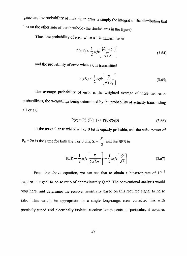
gaussian, the probability of making an ertor is simply the integral of the distribution that
lies on tiie other side of the threshold (the shaded area in the figure).
Thus, the probability of ertor when a 1 is transmitted is
P(e | l )= le r /c V20-,
(3.64)
and tiie probability of error when a 0 is fransmitted
P(e|0) = \erfc - ^ 2 V2cT,
(3.65)
The average probability of ertor is the weighted average of these two enor
probabilities, the weightings being detemiined by the probability of acttially transmitting
a 1 or a 0:
P(e) = P(l)P(e|l) + P(0)P(e|0) (3.66)
In the special case where a 1 or 0 bit is equally probable, and the noise power of
Pn = 2a is the same for both the 1 or 0 bits, S, = ^ - and the BER is 2
BER •erfc 242c
= -erfc 4i
(3.67)
From the above equation, we can see that to obtain a bit-ertor rate of 10"'
requires a signal to noise ratio of approximately Q =7. The conventional analysis would
stop here, and determine the receiver sensitivity based on this required signal to noise
ratio. This would be appropriate for a single long-range, ertor corrected link with
precisely tuned and electrically isolated receiver components. In particular, it assumes
57
that a perfect decision circuit exists at the output of the receiver to perform the threshold
operation
The short range, un-coded links proposed here are in a quite different electrical
environment. They share a silicon IC with high-speed processing circuitry, and as such
are subjected to power supply fluctuations. They are fabbed in a digital CMOS process,
with parameters that vaty from lot to lot and from device to device. The decision circuit
cannot be ignored in the analysis, for its output must conform to the signaling
requirements of the VLSI circuits. This signaling requirement sets a noise margin, which
the output of the decision circuit must meet. Thus, the optical power requirement stated in
equation (3.43) is based on the noise margin required at the output of the decision circuit,
and not the circuit noise of the receiver. However, tiie conventional noise analysis is
useful in that k sets a floor for sensitivity of the receiver.
58

CHAPTER 4
OPTIMIZATION AND SIMULATION
4.1 -Approximate analvsis
Consider the receiver with 1 TIA stage and p VA stages. Summarizing the
equations given in the previous chapter, the speed of the receiver amplifiers is determined
X. by their rise time, tramps - —— • The sensitivity of the receiver amplifiers is given by TZ
a
= A''Zf, which is the fransimpedance gain of the TIA times the gain of the voltage
amplifier.
As a simplified analysis, assume that the gain provides a constant gain-bandwidth
p. GBW product, AvPout =^^ = GBW. Thus, Pout= — — - For the 1- stage TIA, this means
GBW a = where b =2 or the 1-stage TIA.
b.A^
This gain can be written in tenns of maximum bit-rate (i.e. the bit - rate by
assuming tr,in =0 and tr,dc =0):
A . ^ ^ ^ ^ (4.1) " b.X,„.BR
The fransimpedance value can be approximated as
Zf=Rf ^•A (4.2) GBW.C,
where a =2 for the 1-stage TIA.
59
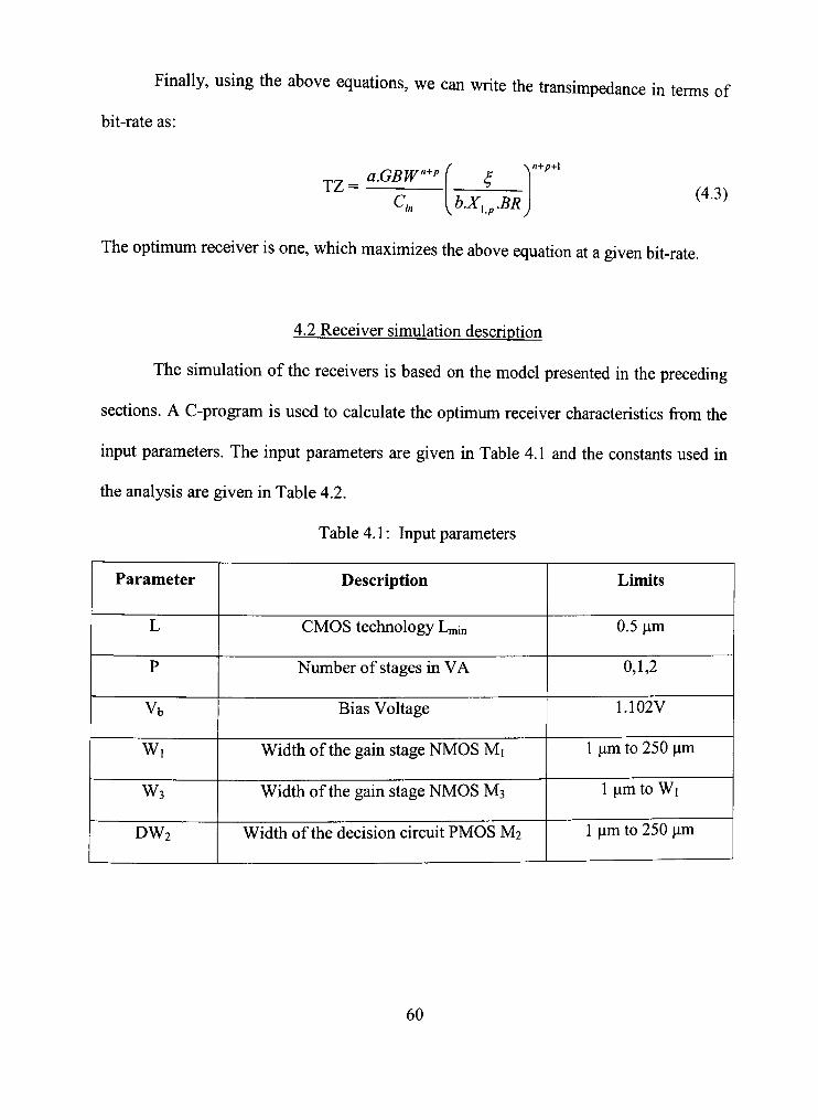
Finally, using the above equations, we can write the transimpedance in tenns of
bit-rate as:
TZ = a.GBW"^"
C,„ ^b.X,,.BRj
n+p+\
(4.3)
The optimum receiver is one, which maximizes the above equation at a given bit-rate.
4.2 Receiver simulation description
The simulation of the receivers is based on the model presented in the preceding
sections. A C-program is used to calculate the optimum receiver characteristics from the
input parameters. The input parameters are given in Table 4.1 and the constants used in
the analysis are given in Table 4.2.
Table 4.1: Input parameters
Parameter
L
P
Vb
Wl
W3
DW2
Description
CMOS technology Lmin
Number of stages in VA
Bias Voltage
Width of the gain stage NMOS Mi
Width of the gain stage NMOS M3
Width of the decision circuit PMOS M2
Limits
0.5 pm
0,1,2
1.102V
1 pm to 250 pm
1 pm to WI
1 pm to 250 pm
60

Table 4.2: Constants used in analysis
Parameter
tr,in
Cpd
Rpd
Idark
r
Description
Input signal rise time
Photodiode capacitance
Photodiode responsivity
Dark current
Gamma for fransistor noise
Limits
L.L Xmin
250 ff^
50%
5nA
2
A photodiode capacitance of 250fF is used on the assumption that the photodiode
which is a reasonable assumption for a standard CMOS 0.5 pm process. The C-program
loops over all values of the input parameters. For each possible combination of
parameters, the program first calculates the feedback resistance necessary to produce a
maximally flat magnittide response. The combination of parameters for which no MFM
solution can be found are discarded. The program then calculates the fransimpedance, bit-
rate and optical power for the MFM solution. The program tiien sorts the receivers
according to the bit-rate and the optimum receiver would be one that minimizes optical
power for the given bit-rate. The parameter values are then used to simulate different
receiver circuits in P-SPICE. P-SPICE simulations are then mn on the optimized
receivers to verify the receiver perfonnance and fimctionality predicted by the model.
61
4.2.1 -Receiver Simulation
In order to verify the fiinctionality and performance of the receiver model and
optimization presented in the previous section, different receiver configurations were
simulated in P-SPICE. This section presents the schematics for the receiver test
stmctures. The results of the simulated receiver model are then given.
4.2.2 -Receiver Schematics
The simulation contained 3 different receiver configurations, with all three of
them optimized for minimum optical power. The model and the optimization program
described in previous chapter was used to find the fransistor sizes for different receiver
configurations. Each receiver configuration was optimized for operation at a different bit-
rate.
Table 4.3 gives the design parameters for the simulated receivers. Listed in the
table are: the receiver configuration (given as 1 + P, where P is the number of gain stages
in the voltage amplifier), the feedback resistance Rf, the gain stage gain Av, and the
modeled values of the bias voltage Vb. Also shown in the Table 4.4 are the optimum
fransistor widths used in simulation.
62

Table 4.3: Simulated receiver design parameters
Receiver
configuration
(1+0)
(1+0)
(1+0)
(1+1)
(1+1)
(1+1)
(1+2)
(1+2)
Input
current
0.1mA
0.06mA
O.lmA
0.1mA
0.05mA
O.lmA
0.04mA
0.03niA
Rf
3.6kQ
6kQ
6kQ
3.6kQ
3.6kQ
2.1kQ
IkQ
1.2kQ
Av
3.23
3.14
3.14
3.2
3.2
3.2
2.2
2.7
Design Vb
I.IV
I.IV
I.IV
I.IV
I.IV
I.IV
I.IV
I.IV
Operation
Speed
(per sec)
1 Gbits
500 Mbits
500 Mbits
700 Mbits
700 Mbits
700 Mbits
500 Mbits
400 Mbits
63

Table 4.4: Simulated receiver transistor widths (0.5 um Technology)
Receiver
Configuration
(1+0)
(1+0)
(1+0)
(1+1)
(1+1)
(1+1)
(1+2)
(1+2)
Ml
30pm
32.5pm
32.5pm
30pm
30pm
30pm
25 pm
32.5pm
M2
2 pm
2 pm
2 pm
2 pm
2 pm
2 pm
1.5 pm
1.5pm
M3
17.5pm
19.16pm
19.16pm
17.5pm
17.5pm
17.5pm
14.72pm
18.89pm
MD,
53.3pm
56.1pm
56.1pm
53.3pm
53.3pm
53.3pm
32pm
35pm
MD2
29.4pm
31.17pm
31.17pm
29.4pm
29.4pm
29.4pm
29.4pm
19.45pm
The complete receiver schematics for the three different receiver configurations
are shown in Figure 4.1, 4.2, and 4.3.
The receiver gain stage consists of fransistors Mi, M2 and M3. Their widtiis are
detennined by the optimization program and given by Table 4.4 and their lengths are the
the process, i.e., 0.5 pm. The gain stage is replicated with its input tied to its minimum in
64

output, to generate the bias voltage Vb. The decision circuit, which thresholds the receiver
signal and produces the final digital voltage swings, consists of transistor Mdi and Md2.
The optimization program also detennines the width of these transistors, and the lengths
are minimum.
One of the assumptions made in this simulation is regarding the photodiode. A
practical possible value for responsivity is assumed for the photodiode and equivalent
curtent that might be generated for incident optical power is simulated with a cunent
pulse source. Other than this assumption, the overall circuit was simulated from the
practical fabricated MOS values and hence, the simulated result and the final fabricated
chip should produce, more or less, the same result.
The feedback resistor is implemented as a parallel combination of NMOS and
PMOS fransistors. The size of these transistors are chosen to be as small as possible, to
reduce the capacitance associated with the feedback resistance. The transistor dimensions
are chosen in such a way to create feedback resistance called for by the optimization
program.
Finally, the Schmitt trigger and super-buffer are implemented as described in
Section 3.2.4. The lengths of all of the fransistors in the digital buffer are the minimum
0.5 pm for highest speed.
65

\m
Jl, HP
m
Vb
- 0
Feeciback Resistor
Vdd
Vb
u*-M2
• * . -
Ipulse ( ^
\^* Ml
Idc
± 1 J: X 4
yaa
Vb
o— n M2
! • * -
JVC —13
vad
H
\/dd • • vad
h rt:
J
. —
'vdd
ri3.3 JlO.9 Jl29.7
HP HP I ^ c . .
\*ld
H3 H?i' Out
U U J
Figure 4.1: Full receiver schematic for 1+0 receiver
66

Vtid
1 1 — •
M2
\m _ 1 r -
H I w* I I I |,„^.,. ,1
Vb
1 0
Ipulse ( A ) ( 4 ^
Fee(3back Resistor
Vtid
Vb
o— J1M2
M1
WJd
0 It*-
V^dd
}1. M2 Vb ^ 1M2
0 It*-
,hJ.. -ri-,K4 .
'I(ic U ^ ^ ^ ^
\M.i Nydd
|-|P-i
,_jlij il l
H >ri HSn
vad
H^
vad
'^3.3 J19 .9 J~|29.7
HP HP
1.1 •>^d
- 1 .
M^M^ Out
Figure 4.2: Full receiver schematic for 1+1 receiver
67
\.«d
j j IM2
Vb
HP Hr' :H M3
Ipulse ( A ) (vy
1 1
Feedback Resistor
\XJd
Vb J I
o \p M2
J
O \n^
•sMd ••M4
n, tut2 Vb J I yl2 Vb J IM2
O I H — I O—
* • .
P
)ldc
T Lj;3i« UD^ L- l^ LJ:^!" Udi« LJpidi
U ^ l ] T] IJ
Vdd Vdd ''^ \* !d •^ \jad
"Iir - i—
H _r
"13.3 J~l9.9 J129.7
HP HP J . I 1 i .
vad
H^ H^ ™' H-H l\ ^ ^
Figure 4.3: Full receiver schematic for 1+2 receiver
68

4.2.3 -Simulation results
111"}! !•--
h tXl
5 cal -
3 flii-0 « W T ^
i.VfT'
2 .1WT"
1>!jf "t
L w ? " ! *
• .S f i -
" I .S* ' -
- I .W"-
-1.58-t-
:i i i1i i!i ' ' i " 1 i ; : i
, < . . ' , I . t
! ; : ; ; : w
: : : ; 1 j : • : ; ^ 1 ; |4 i^t . . • ' 1 i - - x i i
' ? ! | i?' :"'.ft -i—r—:—i—^—p-rtt^.
; ; : ; j; ; ; : !
"'• '»"">' '"' i " y ; ;• ' ;
-. ' ; l ; ;
: ; : ;
; ! • •
; i : ;
i | , , . ; u- i~ < '."'! , , "TTU-:- ' ' i ' • ; ' 1 ; '
i I : !
1 : : ; 1 : ; • ;
4 r H ^ V :
iT^ \ ' \
- .11' i. 1*
..^l\ • ' K : \
J J J - L L 1 ; : : ; T " ; ;"""• ;
• " i ' ' ' • • • ' • ' " • ' • ' • "
\ ) \ I \ r ' ' ' ' " " • • • • - ^ -
: /T~^
'!•• •
(-ii-i
' ; : ^ . :
i ' ; :
i - i - ^
i J . . -f-N' 1
^ ; : ; • ' ' '
. - . . ; ^ . . j . . ^ — i . » .
r: ; 1* l_i
in 1 ' '• t , .
: 1; : t S y - ^ ' f*
' S<wJ..: -4—-
I I i 1 * t • i
t > <
,• •'• i . , , . - ; —
* ' ' '
:/tfir^^ i^ !^
_jli_4£_ :*; :!;
f+^ fc
: ; i ^ •• > H V
) •• 1^
i ; : |i J ; ; 1 TT ; 1 : > + ^ « i ( 1
; ; : :
: : ; ;
: : ; ;
: /ft" it \\ \\\ , ,
'\ \ ; ;
/•rr'Ht-
- ^M i ;
L - J — 1 — i —
> . . 1
11$ i , 1 : i
LiLLL 1J3 TT
'.
i ;
^ ; ; r
'•^^"'Ty"'
' ' ' '
» >/''V"'Y^'
'A''}< \}\ ; :
'i\ : .'
i t ~ ^ _ i . . : _
i'; ; : :L.. :H.d4y: : ;.:
, 1 1 1 — g Jl In, 1 .
lis Ins Jns 3ns hns 5ns 6ns ?n5 Bns 9ns tJos
T iw
Figure 4.4: (1+0) Receiver - 1 Obits/sec output (. 1 mA curtent)
69

DSTIfl:1 U1:Q
fts 2ns Hns 6m Us t»)s 12ii5 1*K tftns iWi zHmiv^ Oi;HJ:gj ^ MM?:!) iUmiH}
Tim
Figure 4.5: (1+0) Receiver - 500 Mbits/sec output (.06 mA current)
70
ISTm:l
Bi 2is te fins Bfis Ifeis 12ns tiins ISns Itni 2Sris B (J(8t:1) U(fl1:l} t «t«?:riji .» (1(111 :dJ
Figure 4.6: (1+0) Receiver - 500 Mbits/sec output (.1 mA curtent)
71

wim:i
65. 1!RS 2iS s *ts Sas fes (Pm:s} 4 ll^fW:i^ «-U(yi:d)
9&5. tftl5
Figure 4.7: (1+1) Receiver - 700 Mbits/sec output (.1 mA current)
72

0S1M1:1 11 ; i !
95 ins 2n5 3ns ims ^m hK a ?cii:+) i(Pie:s) ' U^Pm:s) > Uflt:«) - U{«1;!l]
l ife
7K gw ms
Figure 4.8: (1+1) Receiver - 700 Mbits/sec output (.05 mA cun-ent)
73
osimti lit:Q
3.SU
2.5U
L5U
1.
-8.5U
-2.(
h-+nJ ._:. iJ * —Ul
' ; ; ;
; : ; ;
> ' ' ' , . , ,
: ! : ! m . . . W A ^ ? . . . . . .
> • ' '
; ,v
: : :/!t —^+4
« > . 1
: ; : ; . 1 .
f. : , :
J ; ; ; 1 ; : :
^ T ; •
t : • ; h-U--N . ' .
i — ^ - ^
;« Miii4 , 1 Mmrmw^tMi^rmj , , ^«M n^'-'kirfft^n-nj ,
( 1 -, (
, . ^ 1 , . . ,
NNl Hi I : ; 1 f : ! ; :
1 . 3 . ,
1 • : ; ;
t ; : ; ; ( ; : : :
i***-**!-*-"*'
; • ; •
"+--H ;...,; J-+-" I I \ • '
: i ; ; YrnTTTTrr' - , . , , , , . , . , ,
: ;^; 1 ; : ;- ,T ^ 1 ^ ; :r '• i •
( I - , * 1
r 'J'
i P : ; 1 M ^ : : ; ! ; • ' ;y•i ; 1 : ; ; 111 ; ; ' I ' t F 1
' ^ • . ^ ^ ^ 1 ^
1 J i
: : :
r , . , —Y , - , - — - i « t f
. , . "TT",^—r-T^ : ;,T '
- /
( T' r r r n
Tt^tT i V \ l » 4
i • J -Vr
M:Mi ; : : i M -
::: M i l -• - - J - • : - . . : - .
. ;^?
r-f -P : t"^-^ ; H-t-^^ il. : ; 1 ; ^ : M ; : : T . : ;
: i :: i 1 i : : i 1 i : ; :
* ; ' 1 ! ' ; ' i ' ' T ,„
i I : ; ;
-iJ-iii-; ; : :
* I \ -^ 1 i ( n
^ l : ^ tTl'TT^ 4p~-n )f-^
III',.
; ! ! ; > ' ' f.
',',.' jr
I I ; / : l
; : p •^•^' l j _
"TTfu ' ' • • ' ' J ' V31
: : : :
l i l t
^ Ins 2ns 3ns fens Sns 6ns
l i ne
?n5 las tiis
Figure 4.9: (1+1) Receiver - 700 Mbits/sec output (.1 mA current, Rf- 2kn)
74

U1:t!
te gns te *n5 8ns Ites 1?ns i t e Um Mm 28
Tiw
Figure 4.10: (1+2) Receiver - 400 Mbks/sec output (.03 mA curtent)
75

mm nt:q
8s 2ns kn'j. fes ias Sftis- 12ns l ins 1*jns l^is 28ns n U(fi1:1J iJ(MSrg) •' UOff:fJ i U(ltt:g^ > Hmzi) - U(i1:d,^
Ti*
Figure 4.11: (1+2) Receiver - 500 Mbits/sec output (.04 mA current)
76
4.3 -Transmitter circuit
For VCSEL-based links, the super-buffer drives a final NMOS drive transistor.
This transistor is sized to sink the amount of curtent necessary to produce the required
optical power for the receiver, when the super-buffer output is high. The VCSEL biasing
curtent mirror, ensures that the VCSEL is always biased at (or slightly above) its
threshold current.
The voltage Vbias in Figure 4.4 is determined by the requirement that the NMOS
fransistor stay in saturation when the modulation cunent is flowing through it. The
voltage drop across the VCSEL is set by the threshold voltage Vn, and the extra drop due
to the series resistance Rg. The bias voltage is then
Vbias = V t h + Rslm + V d d - V t n (4.4)
The electrical power dissipated in the VCSEL and average emitted optical power
is given by equations (2.10) and (2.11) respectively.
77

Input
\yad vad ' ^ Vdd
HP ;"l3.3 J l 9 . 9 J~l29.7
HP
H^
HP ,
U ^ f TJ H^'
\ii\as
< Rs
Ml ,
Im
Optical output
M3
\/tid
® Ith
Figure 4.12: VCSEL transmitter circuitry
78

CHAPTER 5
SUMMARY
This thesis investigates the modeling, optimization and simulation of free-space
optical interconnects. As electrical interconnects approach speed and power-scaling
limitations, free-space optical interconnects are under consideration as replacement for
electrical intercormects. Research on the OE device technologies necessary to enable
FSOI has been underway for many years. This thesis addresses the design and
optimization of CMOS circuits to interface to these devices.
The FSOI model was built from bottom up. First, models for modem CMOS and
opto-electronic fransmitting devices were introduced. Then the proposed receiver design
was analyzed and optimized. Finally, the transmitter design was described, enabling the
fiill link to the model.
A mature 0.5 pm CMOS process technology was considered in this analysis.
VCSEL emitters were considered for the OE transmitter. The receiver front-end in this
analysis was a transimpedance amplifier. The receiver was designed with single-ended,
dc-coupled gain stages, and the design was constrained by the requirement for frequency
stability. The optimum receivers were not thermal noise limited - they were limited by
the gain-bandwidth of the CMOS technology and the requirement for CMOS logic levels
at the receiver output. The optimum receiver design (number of stages and fransistor
dimensions) is a fimction of the technology, speed, transmitter efficiency and available
79

optical power. Optimized receivers were simulated in P-SPICE. The output results were
as predicted by the design.
The transmitter driver was modeled as a super-buffer, which drives a fransistor
which sinks a confrolled curtent (for VCSEL emitters). The intrinsic speed of the OE
device is much faster that the CMOS driver circuitry. The size of the super-buffer
determines the speed and power of the transmitter.
Whether FSOI will become a viable interconnect technology depends on many
factors. This thesis has addressed the optimization of the speed/power trade-off of FSOI.
Also important is the yield, cost and availability of proven designs. Despite predictions to
the contrary, electrical interconnect performance continues to improve, through the use of
novel materials, signaling schemes, and architectures. FSOI performance can likewise
benefit from further research into optimized interface circuits. Optimizing the
performance of the end-to-end optical link augments both OE device research and FSOI-
based system design.
80

BIBLIOGRAPHY
1. J.Goodman, F.Leonberger, S.Kung, and R.Athale, "Optical Interconnections for VLSI Systems," Proceedings of the IEEE, vol.72, pp. 850-866,1984.
2. M.Feldman, S.Esener, C.Guest, and S.Lee, "Comparison between optical and electiical interconnects based on power and speed considerations," Applied Optics, vol.27, no.9, pp.3820-3829, 1988.
3. D .Miller, "Physical Reasons for Optical Interconnection," International journal of Optoelectronics, vol.11, pp. 155-68, 1997.
4. D. Miller and H.M. Ozaktas, "Limit to the Bit-Rate Capacity of Electiical Interconnects from the Aspect Ratio of the System Architecture," Journal of Parallel and Distributed Computing, vol.41, pp.42-52, Feb. 1997.
5. D. Miller, "Dense Optical Interconnections for Silicon Electronics," Trends in Optics: Research, Developments, and Applications, vol. 3 of ed. A. Consortini (International Commission for Optics/ Academic Press) pp. 207-222,1995.
6. D. Miller, "Dense two-dimensional integration of optoelecfronics and electronics for intercormections," Critical Reviews Conference on Photonics West Optoelectronics: Jan 24-30, 1998.
7. D.Miller, "Rationale and Challenges for Optical hiterconnects to Elecfronic Chips," Proceedings of IEEE, vol. 88, pp. 728-749, June 2000.
8. A. Krishnamoorthy and D.Miller, "Scaling Optoelectronics-VLSI Circuits into the 21" Century. A Technology Roadmap," Journal Selected Topics in Quantum Electronics, vol 2, pp. 55-76, Apr. 1996.
9. Eilert Berglind, Lars Thylen, "A Comparison of Dissipated Power and Signal-to-Noise Ratios in Electrical and Optical Interconnects," Journal of Lightwave Technology, vol.17 No.l, Jan 1999.
10. J.Goodman, "Fan-in and fan-out with optical interconnects," Optica Acta, vol. 32, pp.1489-1496, 1985.
11. Neil Savage, "Linking with Light," IEEE Spectrum vol. 39, Issue 8, August 2002.
12 I G. Yayla, P.Marchand, and S.Esener, "Speed and Energy Analysis of Digital Interconnections: Comparison of On-Chip, Off-Chip, and Free-Space Technologies, "Applied Optics, vol.37, pp.205-227, Jan 1998.
81

13. Wilm E. Donath, Latency and Rent's Rule, IBM T.J Watson Research Laboratory Yorktown Heights, NY 10598,1998.
14. W.J Dally and J.Poulton, "Transmitter equalization for 4-Gbps signaHng," IEEE Micro, pp 48-56, Jan./Feb.l997.
15. Y.Tsividis, Mixed Analog-Digital VLSI Devices and Technology, McGraw- Hill, New York, 1996.
16. Behzad Razavi, Design of Analog CMOS Integrated Circuits, McGraw-Hill, New York, 2001.
17. M.Steyaert and W.Sansen, "Opamp design towards maximum gain-bandwidth," in Analog Circuit Design, Kluwer Academic Press, New York, 1993.
18. H.C. de Graaff and F.M. Klaassen, Compact Transistor Modeling for Circuit Design, Springer-Verlag, New York, 1990.
19. Yuhua Cheng, Chenming Hu, MOSFET modeling and BSIM3 users's guide, Kluwer Academic Publishers, New York, 1999
20. M.J.M. Pelgrom, A.C. J. Duinmaijer, and A.P.G. Welbers, "Matchkig properties of MOS fransistors, " IEEE J Solid-State Circuits, vol.24, no.5, pp. 1433-9, Oct 1989.
21. P.Kinget and M.Steyaert, "hnpact of transistor mismatch on the speed-accracy-power frade-off of analog CMOS circuks," in Proceedings of the IEEE 1996 Custom Integrated Circuits Conference, 1996, pp.333-6.
22. T.Ackemann, M.Sondermann, "Characteristics of polarization switching in vertical-cavity surface-emitting lasers," Proc.SPIE. 4286, 44, 2001.
23. D.A. Louderback, I.Sjolund, E.R. Hegblom, S. Nakagawa, J.Ko, and L.A. Coldren, "Modulation and free-space link characteristics of monolithically integrated vertical cavity lasers and photodetectors with microlenses," IEEE J.Quantum Electron, vol. 5, no.2, pp. 157-65, March/April 1999.
24. Honeywell Application Sheet for Vertical cavky surface emitting lasers, Honeywell,2002.
82

25.M.H. MacDougal, G.M. Yang, A.E. Bond, C.K. Lin, D.Tishinin, and P D Dapkus, "Electiically-pumped vertical cavity surface emitting lasers with Al O -GaAs reflectors," IEEE Photon Technol Lett., vol. 8, no. 3, pp. 310-2, March
26. M. Govindarajan, S. Sial a, and R. N. Nottenburg, "Optical receiver systems for high speed parallel digital data links," J Lightwave Technol, vol 13 no 7 on 1555-65, July 1995. ' " ' ^^"
27. S. D. Personick, "Receiver design for digital fiber optic communication systems, part i and ii," Bell Syst. Tech. J, vol. 52, no. 6, pp. 843-86, July-Aug. 1973.
28. J. J. Morikuni, A. Dharchoudhury, Y. Leblebici, and S. M. Kang, "hnprovements to the standard theory for photoreceiver noise," IEEE J. Lightwave Technol vol 12, no. 4, pp. 1174-83, July 1994.
29. G. F. Williams, "Lightwave receivers," in Topics in Lightwave Transmission Systems, T. Li, Ed. Academic Press, San Diego, 1991.
30. S. Moustakas and J. L. Hullett, "Noise modeling for broadband amplifier design," lEEProc. G, vol. 128, no. 2, pp. 67-76, April 1981.
31. G. Smith and S. D. Personick, "Receiver design for optical fiber communication systems," in Topics in Applied Physics: Semiconductor Devices for Optical Communication, H. Kressel, Ed., vol. 39, chapter 4, pp. 89-160. Springer Veriag, New York, 1980.
32. A. A. Abidi, "On the choice of optimum FET size in wide-band fransimpedance amplifiers," IEEE J. Lightwave Technol, vol. 6, no. 1, pp. 64-6, January 1988.
33. K. S. Yadav, D. C. Dumka, R. C. Ramola, S. Johri, H. S. Kothari, and B. R. Singh, "Design optimization of three stage GaAs monolithic optical amplifier using SPICE," in Physical Concepts of Materials for Novel Optoelectronic Device Applications II: Device Physics and Applications, 1990, vol. 1362 of Proc.5P/£', pp. 811-9.
34. R. A. Minasian, "Optimum design of a 4-Gbit/s GaAs MESFET optical preamplifier," IEEE J. Lightwave Technol, vol. LT-5, no. 3, pp. 373-9, March 1987.
35. M. B. Das, J.-W. Chen, and E. John, "Designing optoelecfronic integrated J circuit (OEIC) receivers for high sensitivity and maximally flat frequency response," IEEE J. Lightwave Technol, vol. 13, no. 9, pp. 1876-83, September 1995.
83
36. M. J. Kim, D. K. Kim, S. J. Kim, and M. B. Das, "Detennination of bit-rate and sensitivity limits of an optimized p-i-n/HBT OEIC receiver using SPICE simulations," IEEE Trans. Electron Devices, vol. 44, no. 4, pp. 551-7, April 1997.
37. Y. T. Huang, "Optimized integrated CMOS optical receiver for optical interconnects," lEE Proceedings-J, vol. 140, no. 2, pp. 107-14, April 1993.
38. M. Ingels, G. Van der Plas, J. Crols, and M. Steyaert, "A CMOS 18 THzQ 240 Mb/s fransimpedance amplifier and 155 Mb/s LED-driver for low cost optical fiber links," IEEE J. Solid-State Circuits, vol. 29, no. 12, pp. 1552-59, December 1994.
39. T. K. Woodward, A. V. Krishnamoorthy, K. W. Goosen, J. A. Walker, J. E. Cunningham, W. Y. Jan, L. M. F. Chirovsky, S. P. Hui, B. Tseng, D. Kossives, D. Dahringer, D. Bacon, and R. E. Leibenguth, "Clocked-sense-amplifier-based smart-pixel optical receivers," IEEE Photon. Technol. Lett., vol. 8, no. 8, pp. 1067-9, August 1996.
40. S. Sidiropoulos and M. Horowitz, "A 700-Mb/s/pin CMOS signaling interface using curtent integrating receivers," IEEE J. Solid-State Circuits, vol. 32, no. 5, pp. 681-90, May 1997.
41. J. J. Morikuni and S. M. Kang, "An analysis of inductive peaking in photoreceiver design," IEEE J. Lightwave Technol, vol. 10, no. 10, pp. 1426-37, October 1992.
42. D. A. Johns and K. Martin, Analog Integrated Circuit Design, John Wiley and Sons, New York, 1997.
43. J. P. Uyemura, Fundamentals of MOS Digital Integrated Circuits, Addison-Wesley, Reading, MA, 1988.
44. G. F. Williams, "Lightwave receivers," in Topics in Lightwave Transmission Systems, T. Li, Ed. Academic Press, San Diego, 1991.
45. J. G. Graeme, Photodiode Amplifiers: Op Amp Solutions, McGraw-Hill, New York, 1996.
46. D. A. Van Blerkom, C. Fan, M. Blume, and S. C. Esener, "Transimpedance receiver optimization for smart pixel anrays," IEEE J Lightwave Technol, vol. 16, no.l, pp.119-26 January 1998.
84

4J
(U
o
lU
u -H ft 01
(N 4J • H XI u o
<u o s w u H Ck CO
10
U l •H dl
i •.: 6i o
WD H
XI 01 X I U Ol(U Ij c . ^ 10 'H O O It iJ (N O
II) (1)5^-, «01 a H
d) a C 01 c H) M (U H W H . C -H
i •0 U 0 J) 0 -H TJ " Q u e It .. p J jO-H 0)
11) "
3fc 0) n)
* • * *
in o
.H
•a (U
0)
ft o 4J M m V a ^^ w w
0) ft 3
A: I m D
01
a • H 4J 4J (U
CO
T)
m 01
c (U
0 o Q
ID - 0 3
H U
-H
or>
tor>
esist
Res is
CS
r H H
0 0 V V
stor>
Resi
M-l MH • H
Q
a V
stor>
Resi
<tH itH
P
Pl< V
stor>
Resi
01
s B V
stor>
Resi
Cl 01
PQ
pi< V
tor>
tor>
apaci
apaci
u u
A
iiranent
(U
u a n)
4 J 01
- H 01 0) ft!
0
<u
J 3
01
A
Stor:
Laye
1 Resi
.. 01
.tor>
.tor>
lapaci
:apaci
u (-*
A
Comment
CO CO c) nj u j u j O O ' O B P Q O O ' O
V V
ro pi< V
H
P^
^ s
0 -V
g V
2 .
V
PU
v
3 3 3 ro ro CO H i n l o ' J ' II > *
II CO II CO PU CO 0 < Pl<
ft C in — C ro • in in
m • VD H H i n r o
II H H *
en II H • < CO H
~ < i n II
3 H - c o 00 og 3 i n < l O H 0 0 H
^ VO CM 3 II o^ < * 1 r o
Q ti> II i n Cii CN P m II
1 CU . P C -* ^
i n (Ti C o^
3 a\ ( j \
II —. CO i n ci<
in ft r H r -
H o CM
r~ II o CO <N <
1
3 in o
. ro vo c~- in ft >* II ro 1 VD in in <3< ro . .
. H . 1 I - m r H i n • r^ r^
IP C l H CN H p 1 II 1 II
a u. 1 o J 3 J 3 o b rH b H CNl PQ CN PQ CS
II II II S W S W 3
u u
L=2u
SOURi
L=2u
SOUR
L=2u
<n p a*
CSS
3 0 0 f S
ro 3 II
o^ CO t n pij
II CO C
— p i . — i n i n i n H ..^f Qu • <T\
1 r - ( N <N
o ro . i n c^i 1 H
• II II H CO O CO I D < o « ; H f S
1 3 1 3 ( N CTl
rH in in <n i n II . 1 1
1 P CN P pij i n pi<
i n 1
. ft ft ^ o CN r -
O p^ VO CN O O
f S r o 1 i n
- ' II
D 3 PQ VD
II W S CJ
SOUR
L=3u
CO W CO W CO W CO O H O EH O H O 2 < 2 < 2 < S &( O Pij O Pi< O a
3 4 4
DRAIN
5 4 4
DRAIN
5 4 4
(N in ro "i" in 2 S
i n ^ r o
2 * S * S
S VD H
P I -
r o ( N 2
VD
* 2
H r H C>) CN J II 1 II
- § ^ 9 u. w B o B fo PQ CM PQ II
II s W S W U U 3
GATE SOUR
NMOS L=2u
GATE SOUR
5 NMOS L=3
S VD a
S^Sr-P r- P
o VD r~ 0 0 r H
2 2 0 0 r -
* S * 2
3 CO CN
ro II
CO 0<
C i n H CTl
^-. CN
o • ^ T-\
1 II CO
i n <
• .* 3 [~ H r H r H
1 r o II
ro P ^ U\
1
ft i n i n
• C J r - CO r - II
2§ 3
« o
m II 3
W U 3
SOUR
3 L=2
GATE
6 NMO!
a H O
S" p 0 0
r- ro 2
OS
* 2
3 CN H
ro II
CO pi<
~ ft in o
. o i n CT\ r H II - ^ r H CO m
< . i n i n • 3 H
O 00 H
r- o H r o H
1 II CO P H
i n o< 1
^ C in r o i n .
1 r H .^j*
cr> r o i n CN 1
o H ro r - II CO r H P r H
1 < 1
3 U, o U, • J i n J 5 H B PQ II PQ
S
w w CJ 3 U
SOUR
S L=2
SOUR
GATE
6 NMO!
GATE
s a H O H
S " g P CTV Q
<N i n r H
2 2 r H
« 2 •
ft
96763.
CTl H
rM
ro
CTV
o
.—. i n
.<)> CN H
i n
<* VD CM
1
i n
( N CO
i n
H C -
(
MINUS
CO
PU
CT^ CJ
•
959k
c~
c^
n"
o r H
.—. i n
o r-i n
H
o ( N
1
i n
cs ( N
1
i n
H
ro
S (-2
MINU;
en D
o H
pd
«
i n
U P
o
" i "
P
g
i n
U P
VD
O
CO CO
>
ro
CJ
< o\
CO
r H
a H >
t o
CJ
< CTl
O
cs
a H
>

PERMISSION TO COPY
In presenting tiiis thesis in partial fulfillment of the requirements for a master's
degree at Texas Tech University or Texas Tech University Health Sciences Center, I
agree that the Library and my major department shaU make it freely available for
research purposes. Permission to copy this thesis for scholarly purposes may be
granted by the Director of the Library or my major professor. It is understood fliat any
copying or publication of tiiis tiiesis for financial gain shall not be allowed without my
further written permission and tiiat any user may be liable for copyright infringement.
Agree (Permission is granted.)
Student Signature Date
Disagree (Permission is not granted.)
Student Signature Date