THÈSE
En vue de l'obtention du
DDOOCCTTOORRAATT DDEE LL’’UUNNIIVVEERRSSIITTÉÉ DDEE TTOOUULLOOUUSSEE
Délivré par l’Institut Supérieur de l’Aéronautique et de l’Espace Spécialité : Optoélectronique et hyperfréquence
Présentée et soutenue par Ahmad Akhtar HAYAT le 12 octobre 2009
Verrouillage optique des VCSELs émettant à 1.3µm et à 1.5µm : expériences et modélisation
Optical Injection-Locking of 1.3µm and 1.5µm VCSELs :
experiments and Modeling
JURY
M. Eli Kapon, président du jury M. Pascal Besnard, rapporteur M. Philippe Gallion, rapporteur M. Jean-Claude Mollier, co-directeur de thèse Mme Angélique Rissons, directrice de thèse M. Henry White
École doctorale : Génie électrique, électronique et télécommunications
Unité de recherche : Équipe d’accueil ISAE-ONERA OLIMPES Directrice de thèse : Mme Angélique Rissons Co-directeur de thèse : M. Jean-Claude Mollier
Optical Injection-Locking of 1.3µm and 1.5µm
VCSELs: Experiments and Modeling
Ahmad HAYAT
November 5, 2009

Contents
Introduction 15
1 Long Wavelength VCSEL Optical Injection-Locking 19
1.1 Optical Injection Locking . . . . . . . . . . . . . . . . . . . . . . . . . . . . . 19
1.1.1 Introduction and Historical Background . . . . . . . . . . . . . . . . 19
1.2 Emergence of Vertical-Cavity Lasers . . . . . . . . . . . . . . . . . . . . . . . 26
1.2.1 Historical Background and Motivation . . . . . . . . . . . . . . . . . 26
1.2.2 VCSEL Structure . . . . . . . . . . . . . . . . . . . . . . . . . . . . . 28
1.2.3 Performance Drawbacks . . . . . . . . . . . . . . . . . . . . . . . . . 30
1.2.3.1 DBR Growth . . . . . . . . . . . . . . . . . . . . . . . . . . 30
1.2.3.2 Optical and Electrical Confinement . . . . . . . . . . . . . . 31
1.2.4 The Tunnel Junction . . . . . . . . . . . . . . . . . . . . . . . . . . . 32
1.2.5 Technological Breakthroughs and Advances in Long Wavelength VCSEL
Fabrication . . . . . . . . . . . . . . . . . . . . . . . . . . . . . . . . 34
1.3 Emergence of Long Wavelength VCSELs . . . . . . . . . . . . . . . . . . . . 35
1.3.1 Vertilas VCSELs . . . . . . . . . . . . . . . . . . . . . . . . . . . . . 36
1.3.2 BeamExpress VCSELs . . . . . . . . . . . . . . . . . . . . . . . . . . 38
1.3.2.1 Wafer Fusion . . . . . . . . . . . . . . . . . . . . . . . . . . 38
1.3.2.2 Localized Wafer Fusion . . . . . . . . . . . . . . . . . . . . 38
1.3.3 RayCan VCSELs . . . . . . . . . . . . . . . . . . . . . . . . . . . . . 39
1.4 Long Wavelength VCSEL Direct Modulation . . . . . . . . . . . . . . . . . . 40
1.4.1 Need for VCSEL Optical Injection-Locking . . . . . . . . . . . . . . . 40
1.4.1.1 Phase-Amplitude Coupling . . . . . . . . . . . . . . . . . . 41
1.4.1.2 Intrinsic Modulation Limits . . . . . . . . . . . . . . . . . . 42
1.5 Long Wavelength VCSEL Optical Injection-Locking . . . . . . . . . . . . . . 42
2 Simulation of Optically Injection-Locked VCSELs 53
2.1 VCSEL Rate Equations . . . . . . . . . . . . . . . . . . . . . . . . . . . . . 53
2.2 Locking Range Calculations . . . . . . . . . . . . . . . . . . . . . . . . . . . 55
2.3 Small Signal Analysis . . . . . . . . . . . . . . . . . . . . . . . . . . . . . . . 59
2.3.1 Theory and Physical Explanation . . . . . . . . . . . . . . . . . . . . 62
2.4 Numerical Simulations . . . . . . . . . . . . . . . . . . . . . . . . . . . . . . 65
3
CONTENTS
2.4.1 VCSEL Intrinsic Parameters . . . . . . . . . . . . . . . . . . . . . . . 65
2.4.2 Simulation Results . . . . . . . . . . . . . . . . . . . . . . . . . . . . 65
2.4.2.1 High Resonance Frequency, Low Bandwidth . . . . . . . . . 66
2.4.2.2 High Resonance Frequency, High Bandwidth . . . . . . . . . 68
2.4.2.3 Low Resonance Frequency, Low Bandwidth . . . . . . . . . 69
2.5 Comparison between Free-Running and Injection-Locked VCSEL Models . . 70
2.6 Conclusion and Discussion . . . . . . . . . . . . . . . . . . . . . . . . . . . . 71
3 Optical Injection-Locking Experiments 75
3.1 Experiments using Multimode Lasers . . . . . . . . . . . . . . . . . . . . . . 75
3.1.1 Multimode Edge Emitting Lasers (EELs) . . . . . . . . . . . . . . . . 75
3.1.2 Multimode VCSELs . . . . . . . . . . . . . . . . . . . . . . . . . . . 76
3.2 Experiments using Single-Mode VCSELs . . . . . . . . . . . . . . . . . . . . 79
3.2.1 Experiments Using Vertilas VCSELs . . . . . . . . . . . . . . . . . . 79
3.2.2 Experiments Using BeamExpress VCSELs . . . . . . . . . . . . . . . 81
3.2.2.1 Optical Injection-Locking Measurement Results . . . . . . . 84
3.2.2.2 High Resonance Frequency, High Bandwidth . . . . . . . . . 84
3.2.2.3 Low Resonance Frequency, Low Bandwidth . . . . . . . . . 86
3.2.2.4 High Resonance Frequency, Low Bandwidth . . . . . . . . . 86
3.2.3 Experiments Using RayCan VCSELs . . . . . . . . . . . . . . . . . . 89
3.2.3.1 RayCan VCSELs Structure . . . . . . . . . . . . . . . . . . 89
3.2.3.2 Injection Locking Experiments . . . . . . . . . . . . . . . . 93
3.3 Measurement Simulation Comparison . . . . . . . . . . . . . . . . . . . . . . 94
3.4 Conclusion and Discussion . . . . . . . . . . . . . . . . . . . . . . . . . . . . 95
4 Frequency Response Extraction and RIN Measurements 99
4.1 Frequency Response Subtraction . . . . . . . . . . . . . . . . . . . . . . . . . 99
4.1.1 Extraction Procedure . . . . . . . . . . . . . . . . . . . . . . . . . . . 99
4.1.1.1 Mathematical Model . . . . . . . . . . . . . . . . . . . . . . 100
4.1.1.2 Experimental Results . . . . . . . . . . . . . . . . . . . . . . 100
4.1.1.3 Fitting Procedure . . . . . . . . . . . . . . . . . . . . . . . . 102
4.1.1.4 1550 Fibered RayCan VCSELs . . . . . . . . . . . . . . . . 104
4.1.2 Injection-Locked VCSELs . . . . . . . . . . . . . . . . . . . . . . . . 106
4.1.2.1 Injection-Locked Fibered RayCan VCSELs . . . . . . . . . . 106
4.2 Relative Intensity Noise (RIN) measurements . . . . . . . . . . . . . . . . . 109
4.2.1 RIN Measurements of Injection-Locked VCSELs . . . . . . . . . . . . 113
4.2.1.1 Negative Wavelength Detuning Regime . . . . . . . . . . . . 114
4.2.1.2 Positive Wavelength Detuning Regime . . . . . . . . . . . . 116
4.2.1.3 RIN Improvement . . . . . . . . . . . . . . . . . . . . . . . 117
4.3 Conclusion and Discussion . . . . . . . . . . . . . . . . . . . . . . . . . . . . 118
Conclusion and Future Prospects 121
4

CONTENTS
List of Publications 127
5


List of Figures
1.1 Title of Christiaan Huygens’ “Horlogium Oscillatorium”: An early 18th cen-
tury reprint (1723). . . . . . . . . . . . . . . . . . . . . . . . . . . . . . . . . 20
1.2 Locking setup of two electronic oscillators proposed by Adler. . . . . . . . . . 21
1.3 The test bench proposed by Stover and Stier for the first Optical Injection-
Locking experiment using two He-Ne lasers emitting in the 650nm range. . . 21
1.4 (i) Free-running follower linewidth against its reciprocal output power P−1f (ii)
Master linewidth against its reciprocal output power P−1m (iii) Injection-locked
follower linewidth against reciprocal output power P−1m [10]. . . . . . . . . . 23
1.5 Demonstration of frequency response improvement of an injection-locked laser
with increasing injected optical power by Meng et. al [19]. . . . . . . . . . . 25
1.6 Schematic representation of far-field emission of a stripe-geometry Double
Heterostructure (DH) laser. The full angles at half power, perpendicular to
and along the junction plane, are indicated [20]. . . . . . . . . . . . . . . . . 26
1.7 An early design schematic for top-emitting and botton-emitting VCSELs pre-
sented by Jewell et. al. in 1989. . . . . . . . . . . . . . . . . . . . . . . . . . 27
1.8 Refractive indices of AlAs and Al0.1Ga0.9As as a function operating wavelengths. 29
1.9 Calculated reflectivity of an AlAs-Al0.1Ga0.9As multilayer semiconductor Bragg
reflector as a function of the number of pairs [30]. . . . . . . . . . . . . . . . 30
1.10 Thermal conductivity of the various alloy compositions of the InGaAlAs Ma-
terial System plotted versus free lattice constant and band gap energy. The
line indicates the quaternary compositions that can be used for DBRs on InP.
[32] . . . . . . . . . . . . . . . . . . . . . . . . . . . . . . . . . . . . . . . . . 31
1.11 Static current-voltage characteristics of a typical tunnel diode. Ip and Vp are
the peak current and peak voltage. Iv and Vv are the valley current and valley
voltage. The balck circle signifies operation in reverse bias conditions.[20]. . . 33
1.12 Energy-band diagram of tunnel diode in reverse bias state [20]. . . . . . . . . 33
1.13 A long wavelength VCSEL with a tunnel junction emitting at 1.55µm pre-
sented by Boucart et. al in 1999. . . . . . . . . . . . . . . . . . . . . . . . . 35
1.14 A Vertilas BTJ structure with an emission wavelength of 1.55µm [31]. . . . . 36
1.15 Schematic diagram of a wafer-fused Beam-Express VCSEL with an emission
wavelength of 1.5µm. . . . . . . . . . . . . . . . . . . . . . . . . . . . . . . . 39
7

LIST OF FIGURES
1.16 Calculated reflectivity of different materials used as semiconductor Bragg re-
flectors as a function of the number of pairs [57]. . . . . . . . . . . . . . . . . 40
1.17 MOVCD Grown monolithic structure of a 1.5µm RayCan VCSEL. . . . . . . 41
1.18 Improved frequency response of an injection-locked VCSEL emitting at 1.55µm.
The VCSEL is injection-locked using a DFB laser [64]. . . . . . . . . . . . . 43
1.19 Comparison between the chirp of (a) a directly modulated free-running and
(b) an injection-locked VCSEL. The VCSEL is injection-locked using a DFB
laser [64]. . . . . . . . . . . . . . . . . . . . . . . . . . . . . . . . . . . . . . 44
2.1 A general schematic representation of the measurement setup employed for
injection-locking experiments. (a) The transmission setup, usually employed
for double edge-emitting semiconductor lasers, (b) The reflection setup, usu-
ally employed for single-side emission lasers. . . . . . . . . . . . . . . . . . . 53
2.2 Calculated locking range of a long wavelength VCSEL with αH = 7. . . . . . 57
2.3 2D presentation of calculated locking range of a long wavelength VCSEL with
αH = 3 showing the locking-range dependence on injected optical power. . . 57
2.4 Resonance frequencies reported by different groups working on optical injection-
locking of semiconductor lasers [6]. The shaded region signifies VCSELs while
the un-shaded region represents the EELs. . . . . . . . . . . . . . . . . . . . 58
2.5 A schematic diagram representing the physical phenomenon of resonance fre-
quency enhancement of the follower VCSEL due to optical injection-locking.
The beat note ωmaster − ωDownshifted created due to frequency-mixing inside
the follower VCSEL optical cavity is amplified due to resonance when a signal
with a same frequency value is applied to modulate the follower VCSEL. . . 64
2.6 Calculated S21 response of an optically injection-locked VCSEL with constant
frequency detuning and variable injection power from -60 dBm to -40 dBm. . 66
2.7 Calculated S21 response of an optically injection-locked VCSEL with constant
injected power and variable positive frequency detuning. The detuning is
varied from 10 GHz to 110 GHz. . . . . . . . . . . . . . . . . . . . . . . . . . 67
2.8 Simulated S21 response of an optically injection-locked VCSEL. The injected
optical power is kept constantwhile the resonance frequency increases with
increasing detuning frequencies. . . . . . . . . . . . . . . . . . . . . . . . . . 67
2.9 Simulated S21 response of an optically injection-locked follower VCSEL show-
ing cut-off frequency enhancement. . . . . . . . . . . . . . . . . . . . . . . . 68
2.10 Calculated S21 response of an optically injection-locked VCSEL with constant
injected power and variable negative detuning. The detuning is varied from
10 GHz to -190 GHz. . . . . . . . . . . . . . . . . . . . . . . . . . . . . . . . 69
2.11 Comparison between the free-running and injection-locked transfer functions
of a VCSEL. . . . . . . . . . . . . . . . . . . . . . . . . . . . . . . . . . . . . 70
2.12 Free-Running VCSEL S21 response calculated by putting Sinj and ∆ω equal
to zero in equations 2.5, 2.6 and 2.7. . . . . . . . . . . . . . . . . . . . . . . 70
8

LIST OF FIGURES
3.1 The super-imposed spectra of a free running and an injection locked Fabry-
Pérot EEL. Mode suppression can be observed in the injection locked spectrum. 75
3.2 2D presentation of calculated locking range of a long wavelength VCSEL with
αH = 3 showing the locking-range dependence on injected optical power. . . 76
3.3 Optical spectrum of an Vertilas multimode “Power” VCSEL. The VCSEL
threshold current is about 6 mA. . . . . . . . . . . . . . . . . . . . . . . . . 77
3.4 Spectrum of an optically injection-locked multimode Vertilas VCSEL. The
threshold current is about 6 mA. A very feeble side-mode suppression is ob-
served due to injection-locking. . . . . . . . . . . . . . . . . . . . . . . . . . 77
3.5 L-I curve (a) and Optical spectrum (b) of a Vertilas VCSEL with an emission
wavelength of 1.55µm. . . . . . . . . . . . . . . . . . . . . . . . . . . . . . . 79
3.6 Test-bench used for Vertilas 1.55µm VCSEL optical injection-locking mea-
surements. . . . . . . . . . . . . . . . . . . . . . . . . . . . . . . . . . . . . . 80
3.7 Simultaneous presentation of the master and follower laser optical spectra.
The master laser is a tunable external cavity laser while the follower laser is
a Vertilas single mode 1.56µm VCSEL. . . . . . . . . . . . . . . . . . . . . . 80
3.8 (a) Optical spectrum of an optically injection-locked Vertilas VCSEL. The
locking of fundamental mode further suppresses the side-mode. (b) Optical
spectrum of an optically injection-locked Vertilas VCSEL. The locking of side
mode has suppressed the fundamental lasing mode. Notice the position of the
suppressed modes in the two different cases. . . . . . . . . . . . . . . . . . . 81
3.9 Optical injection-locking setup using a polarization maintaining optical circu-
lator. A semiconductor optical amplifier (SOA) connected to port 1 is used
to vary the injected optical power. . . . . . . . . . . . . . . . . . . . . . . . . 82
3.10 Schematic representation of the experimental setup used to measure the S21
response of an on-chip VCSEL using a vector network analyzer. . . . . . . . 82
3.11 The L-I curves for the first set of BeamExpress VCSELs used in this experi-
ment. Representative wavelength-bias current tuning curves are also given. . 83
3.12 The L-I curves for the second set of BeamExpress VCSELs used in this ex-
periment. Representative wavelength-bias current tuning curves are also given. 83
3.13 S21 response of an optically injection-locked single mode BeamExpress VCSEL
emitting at 1.3µm. . . . . . . . . . . . . . . . . . . . . . . . . . . . . . . . . 84
3.14 S21 response of an optically injection-locked single mode BeamExpress VCSEL
emitting at 1.3µm. Several S21 curves are obtained with increasing injected
optical power for a constant negative frequency detuning. P1>P2>P3>P4 . . 85
3.15 Cut-Off frequency variation of injection-locked BeamExpress VCSELs with
increase in optical injected power. All the measurements were made in the
negative detuning frequency operation regime. . . . . . . . . . . . . . . . . . 85
3.16 S21 response of an optically injection-locked single mode BeamExpress VCSEL
emitting at 1.3µm. The VCSEL is injection-locked at a slightly positive de-
tuning frequency. . . . . . . . . . . . . . . . . . . . . . . . . . . . . . . . . . 86
9

LIST OF FIGURES
3.17 S21 response of an optically injection-locked single mode BeamExpress VCSEL
emitting at 1.3µm and operating in the positive detuning frequency regime.
The master and follower VCSEL bias currents are 6.75mA and 7.4 mA re-
spectively. . . . . . . . . . . . . . . . . . . . . . . . . . . . . . . . . . . . . . 87
3.18 S21 response of an optically injection-locked single mode BeamExpress VCSEL
emitting at 1.3µm and operating in the positive detuning frequency regime.
The master and follower VCSEL bias currents are 6.75 and 7.84 mA respec-
tively. . . . . . . . . . . . . . . . . . . . . . . . . . . . . . . . . . . . . . . . 88
3.19 S21 response of an optically injection-locked single mode BeamExpress VCSEL
emitting at 1.3µm and operating in the positive detuning frequency regime. 88
3.20 MOVCD Grown monolithic structure of a 1.5µm RayCan VCSEL. . . . . . . 90
3.21 Bottom-emitting on-chip RayCan VCSEL with 1.3µm operation wavelength. 90
3.22 1.3µm RayCan VCSEL with sub-mount. . . . . . . . . . . . . . . . . . . . . 91
3.23 Free-running S21 response of a RayCan VCSEL emitting at 1.3µm. . . . . . 92
3.24 Schematic representation of the test-bench employed for injection-locking ex-
periments using RayCan VCSELs emitting at 1.3µm. . . . . . . . . . . . . . 92
3.25 S21 response of an optically injection-locked RayCan VCSEL emitting at
1.3µm operating in the positive frequency detuning regime. . . . . . . . . . . 92
3.26 S21 response of an optically injection-locked RayCan VCSEL emitting at
1.3µm operating in the negative frequency detuning regime. . . . . . . . . . 93
3.27 Comparison between the experimental and simulated S21 response of an opti-
cally injection-locked BeamExpress VCSEL emitting at 1.3µm. . . . . . . . . 94
3.28 Comparison between the experimental and simulated S21 response of an opti-
cally injection-locked BeamExpress VCSEL emitting at 1.3µm. . . . . . . . . 94
3.29 Comparison between the experimental and simulated S21 response of an opti-
cally injection-locked BeamExpress VCSEL emitting at 1.3µm. . . . . . . . . 95
4.1 Calculated S21 response curves for different bias currents. . . . . . . . . . . . 101
4.2 1.3µm RayCan VCSEL experimental S21 response curves for different bias
currents. . . . . . . . . . . . . . . . . . . . . . . . . . . . . . . . . . . . . . . 102
4.3 1.3µm RayCan VCSEL subtracted experimental S21 response curves for dif-
ferent bias currents. . . . . . . . . . . . . . . . . . . . . . . . . . . . . . . . . 103
4.4 1.3µm RayCan VCSEL subtracted calculated S21 response curves for different
bias currents. . . . . . . . . . . . . . . . . . . . . . . . . . . . . . . . . . . . 103
4.5 Comparison between measured and calculated subtracted responses for a bias
current of 8mA before the application of fitting procedure. . . . . . . . . . . 104
4.6 Comparison between measured, calculated and fitted subtracted responses for
a bias current of 8mA after the application of fitting procedure. . . . . . . . 104
4.7 Reconstructed S21 response curves using the Y and Z values presented in
Table. 4.3. . . . . . . . . . . . . . . . . . . . . . . . . . . . . . . . . . . . . . 105
10
LIST OF FIGURES
4.8 1.5µm RayCan VCSEL experimental S21 response curves for different bias
currents. . . . . . . . . . . . . . . . . . . . . . . . . . . . . . . . . . . . . . . 105
4.9 Reconstructed S21 response curves using the Y and Z values presented in
Table. 4.3. . . . . . . . . . . . . . . . . . . . . . . . . . . . . . . . . . . . . . 106
4.10 Optically injection-locked follower VCSEL S21 response curves presented by
Chrostowski et al. in [6]. . . . . . . . . . . . . . . . . . . . . . . . . . . . . . 107
4.11 RayCan 1.5µm optically injection-locked follower VCSEL S21 response curves
for different incident optical powers. . . . . . . . . . . . . . . . . . . . . . . . 108
4.12 Subtracted calculated optically injection-locked follower VCSEL S21 response
curves for different incident optical powers. . . . . . . . . . . . . . . . . . . . 108
4.13 Reconstructed S21 response curves for injection-locked 1.5µm RayCan VCSELs.
The detuning is kept constant at 10 GHz. . . . . . . . . . . . . . . . . . . . 109
4.14 Example of noise in modulated laser signal for analog applications. . . . . . . 110
4.15 Testbench for RIN measurements of 1.5µm free-running Raycan VCSELs . . 110
4.16 RIN measurements for a 1.55µm RayCan VCSEL for different bias currents. 111
4.17 Peak RIN plotted as a function of increasing bias current. The black dots
signify the peak RINs for different bias currents, while the solid red line is the
mathematical fit. . . . . . . . . . . . . . . . . . . . . . . . . . . . . . . . . . 112
4.18 Testbench for RIN measurements of injection-locked 1.5µm Raycan VCSELs. 113
4.19 Tunable laser RIN curves for various bias currents . . . . . . . . . . . . . . . 114
4.20 RIN measurements for an injection-locked 1.55µm RayCan VCSEL for differ-
ent optical incident powers. The VCSEL is injection-locked on the positive
frequency detuning edge of the locking-range. . . . . . . . . . . . . . . . . . 115
4.21 RIN measurements for an injection-locked 1.55µm RayCan VCSEL for differ-
ent optical incident powers. The VCSEL is injection-locked on the negative
frequency detuning edge of the locking-range. . . . . . . . . . . . . . . . . . 115
4.22 Comparison between the measured 1.5µm RayCan VCSEL RIN under differ-
ent operating conditions. The three different curves present the RIN under
free-running, positive wavelength detuning and negative wavelength detuning
regimes. . . . . . . . . . . . . . . . . . . . . . . . . . . . . . . . . . . . . . . 116
4.23 Comparison between the free-running and injection-locked 1.5µm RayCan
VCSEL RIN spectra. . . . . . . . . . . . . . . . . . . . . . . . . . . . . . . . 117
11


List of Tables
1.1 Long Wavelength VCSEL Fabrication Development Chronology . . . . . . . 37
2.1 Long wavelength VCSEL intrinsic parameters used to simulate the small-
signal injection-locking behavior[15]. . . . . . . . . . . . . . . . . . . . . . . 65
3.1 Injected photon density and frequency detuning values for the calculated
curves presented in figures 3.27, 3.28 and 3.29. . . . . . . . . . . . . . . . . . 95
4.1 Long wavelength VCSEL intrinsic parameters used to simulate the small-
signal [3]. . . . . . . . . . . . . . . . . . . . . . . . . . . . . . . . . . . . . . 101
4.2 Initial values used to calculate the best-fit between calculated and experimen-
tal curves. . . . . . . . . . . . . . . . . . . . . . . . . . . . . . . . . . . . . . 103
4.3 Final values of Y and Z parameters for different bias currents after the fitting
procedure. . . . . . . . . . . . . . . . . . . . . . . . . . . . . . . . . . . . . . 105
13

Introduction
Since the telecommunication revolution in the early 90s, that saw massive deployment of
optical fiber for high bit rate communications, coherent optical sources have made tremen-
dous technological advances. The technological improvement has been multi dimensional;
component sizes have been reduced, conversion efficiencies increased, power consumptions
decreased and integrability into compact optoelectronic sub-modules improved. Semicon-
ductor lasers, emitting in the 1.1-1.6 µm range, have been the most prominent beneficiaries
of these technological advances. This progress is a result of research efforts, that consistently
came up with innovative solutions and components, to meet the market demand. This in-
phase, demand and supply, problem and solution and consumer need and innovation cycle,
has ushered us in to the present information technology era, where stable high speed data
links make the backbone of almost every aspect of life, from economy to entertainment and
from health sector to defense production.
By the start of twenty-first century, a new, low cost, low power consumption and
miniaturized generation of lasers had started to capture its own market share. These lasers,
named Vertical-Cavity Surface-Emitting Lasers (VCSELs) due to the presence of an optical
cavity which is normal to the fabrication plane , have established themselves as premier
optical sources in short-haul communications such as Gigabit ethernet, in optical computing
architectures and in optical sensors. While shorter wavelength VCSEL (< 1µm) fabrication
technology was readily mastered, due to the ease in manipulation of AlGaAs-based materials,
long wavelength VCSELs especially VCSELs emitting in the 1.3-1.5 µ range have encoun-
tered several technical challenges. There importance as low-cost coherent optical sources for
the telecommunication systems is primordial, since they are compatible with the existing
infrastructure.
VCSEL utilization in low-cost systems imply the application of direct modulation for
high bit rate data transmission which engenders the problems of frequency chirping which
increases laser linewidth and severely limits the system performance. Furthermore, relatively
lower VCSEL intrinsic cut-off frequencies translated in to impossibility of achieving high bit
rates. Optical injection-locking is proposed as a solution to these problems. It enhances the
intrinsic component bandwidth and reduces frequency chirp considerably [1].
15
Introduction
The motivation of this research work is the demonstration of long wavelength VCSEL
optical injection-locking phenomena under different varying system parameters and con-
ditions. The research work was undertaken in the context of a European project in col-
laboration with Ecole Polytechnique Fédérale de Lausanne (EPFL), D-Lightsys, a French
company which specializes in optical sub-assembly integration and BeamExpress, a Swiss
VCSEL fabrication spin-off. Most of the VCSELs used in the injection-locking experiments
in the course of this work have been provided by BeamExpress [2]. VCSELs fabricated by the
South Korean manufacturer RayCan have also been employed [3]. The experimental stud-
ies have been complemented by undertaking the development of a comprehensive, VCSEL
intrinsic parameter-based mathematical model. The experimental results and the mathemat-
ical model have been used simultaneously to investigate optical injection-locking phenomena.
The first chapter introduces the historical background on optical injection-locking. It
then explains the evolution of optical injection-locking experiments and techniques since the
discovery of laser itself. Optical injection-locking in the context of in-plane lasers is then
introduced which then logically leads to the optical injection-locking of VCSELs. Several dif-
ferent applications of VCSEL optical injection-locking vis à vis its different operation regimes
are then discussed.
The second chapter is dedicated to the mathematical modeling of optically injection-
locked VCSELs. A modified rate-equation based mathematical model is presented. This
model uses the VCSEL intrinsic parameters values to calculate the system frequency re-
sponse. System S21 response under various injection conditions as well as for different
frequency detuning values have been investigate. Stable VCSEL optical injection-locking
operation range, in terms of detuning frequency and injected optical power, have been cal-
culated. A comparison between free-running and injection-locked VCSEL models has also
been presented.
The third chapter deals with the experimental studies of optically injection-locked
VCSELs. Results obtained by the optical injection-locking of on-chip VCSELs have been
presented. Several different operation regimes have been investigated. Finally a comparison
between the injection-locking measurements and the simulations developed in the second
chapter is presented.
The fourth chapter deals with the injection-locking of fibered VCSELs and the Relative
Intensity Noise (RIN) of VCSELs. An extraction methodology has been developed in order
to extract the component S21 response from the noisy system response. This methodology is
implemented on both free-running and injection-locked VCSELs. RIN measurements of free-
running and injection-locked VCSELs have been presented. RIN measurements have been
used to observe the resonance peaks of fibered VCSELs which were otherwise unobservable.
A comparison of free-running and injection-locked VCSEL RINs is presented.
16

Introduction
Bibliography
[1] C.-H. Chang, L. Chrostowski, and C. Chang-Hasnain, “Injection locking of VCSELs,”
IEEE Journal of Selected Topics in Quantum Electronics, vol. 9, no. 5, pp. 1386–1393,
Sept.-Oct. 2003.
[2] V. Iakovlev, G. Suruceanu, A. Caliman, A. Mereuta, A. Mircea, C.-A. Berseth, A. Syrbu,
A. Rudra, and E. Kapon, “High-Performance Single-Mode VCSELs in the 1310-nm Wave-
band,” IEEE Photonics Technology Letters, vol. 17, no. 5, pp. 947–949, May 2005.
[3] M.-R. Park, O.-K. Kwon, W.-S. Han, K.-H. Lee, S.-J. Park, and B.-S. Yoo, “All-epitaxial
InAlGaAs-InP VCSELs in the 1.3-1.6-µm Wavelength Range for CWDM Band Applica-
tions,” IEEE Photonics Technology Letters, vol. 18, no. 16, pp. 1717–1719, Aug. 2006.
17

Chap
ter
1 Long Wavelength VCSEL Op-
tical Injection-Locking
1.1 Optical Injection Locking
1.1.1 Introduction and Historical Background
In 1665 Christiaan Huygens, the eminent Dutch mathematician, scientist and astronomer,
later to become famous for the discovery of Saturn Rings 1, while confined to bed through
illness, remarked that the pendulums of two clocks in his bedroom locked synchronously
if they were hung close to each other but became free-running when the distance between
them was increased. Huygens concluded through this thought experiment that the mechan-
ical vibrations transferred from one clock to the other via the wall were responsible for this
synchronization, thus providing the first observation of coupling of two oscillators. One
pendulum injected small perturbations through the wall to the other pendulum eventually
locking the phase and the frequency of the two pendulums together. Huygens later detailed
this idea in his work “Horologium Oscillatorium” [1].
Huygens observations provided the basis for locking of mechanical oscillators. Although
Huygens did contribute enormously to wave and light propagation theories, he never tried
to apply the concepts of mechanical oscillator synchronization to light sources. This can
of course be explained by the inexistence, at that time, of electronic and optoelectronic
oscillator devices. Approximately 300 years later, in 1946, Adler [2] published his seminal
works on the synchronization and therefore locking of two electronic oscillators.
He injection-locked a crystal oscillator with an external frequency source. Adler ex-
trapolated the mechanical oscillator synchronization principles observed by Huygens to the
electrical domain. He showed that when an external signal of frequency ωext is injected into
an oscillator with an oscillation frequency of ω0, the circuit now oscillates at the injected
frequency, given that the injected frequency ωext is close to the natural oscillation frequency
ω0 of the circuit. Injection-Locking of electronic oscillators was thus brought to the fore.
Optical Injection-Locking, however, had to wait another 20 years for its first experi-
mental demonstration. In 1965, Pantell expanded Adler’s theory to include a generalized
behavioral model for lasers under optical injection-locking mechanisms [3] and finally in 1966
1The brighter interior of the “Orion Nebula” bears the name of the Huygens Region in his honor.
19
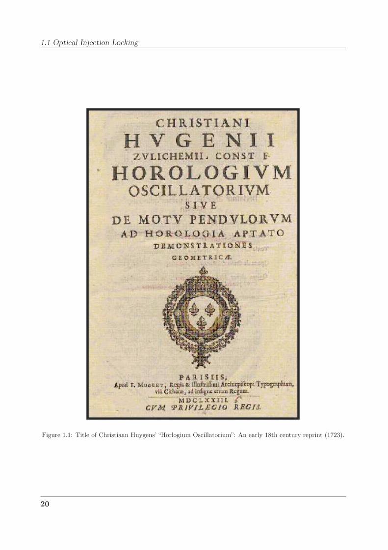
1.1 Optical Injection Locking
Figure 1.1: Title of Christiaan Huygens’ “Horlogium Oscillatorium”: An early 18th century reprint (1723).
20

Chapter 1 : Long Wavelength VCSEL Optical Injection-Locking
E
E1
LRC
RT
CT
Eg
Ef
Figure 1.2: Locking setup of two electronic oscillators proposed by Adler.
Stover and Steier demonstrated the optical injection-locking for the first time using two He-
Ne lasers emitting in the 650nm range [4]. In this experiment the beam from one He-Ne laser
was directly injected into the cavity of another He-Ne laser operating at the same wavelength.
Piezoelectric Transducers
Follower Laser
Master Laser
Beam Splitter Mirror
Beam Splitter
Beam Splitter
Lead Lined Boxes
CRO
Isolator +
Polarization Controller
Photo Tube
Figure 1.3: The test bench proposed by Stover and Stier for the first Optical Injection-Locking experiment
using two He-Ne lasers emitting in the 650nm range.
Optical Injection-Locking, after its first demonstration, slowed down considerably for
the next decade. This can be explained by the fact that lasers themselves were incipient at
that time and new materials and techniques for laser fabrication were being developed. Fur-
thermore, laser systems used crystals, gases or dyes as gain components which rendered the
systems bulky and inefficient. Attempts to injection-lock these optical oscillators were thus
few and far between and energies were focused more on the development of compact, lighter
and efficient optical sources. Throughout the 70’s the progress on the optical injection-
21
1.1 Optical Injection Locking
locking remained rather slow. The major emphasis was to apply Stover and Steier’s He-Ne
optical injection-locking demonstration to other laser systems. In 1972, for example, Buczek
and Freiburg demonstrated the optical injection-locking using two CO2 lasers [5].
The development, arrival and maturation of optical fibers in the mid and late 70’s
acted as a catalyst for the conception, development and mass fabrication of semiconductor
lasers. This opened-up an explosive growth potential in telecommunications and in related
fields such as direct and coherent detection. As a consequence of the availability of cheaper,
compact and relatively more efficient GaAs and InP based semiconductor lasers, the optical
injection-locking research took-off in the 80’s. Subsequent to these developments almost all
the injection-locking experiments were carried-out using the semiconductor lasers.
The 1980’s experienced a rapid development in the optical injection-locking domain.
Kobayashi and Kimura revived the injection-locking research when, in 80, they demonstrated
for the first time the optical injection-locking using two AlGaAs lasers emitting at 840nm[6].
The 80’s also saw an increase in the employment of injection-locking techniques in the co-
herent detection of modulated optical signals. Coherent detection of a modulated signal
was particularly popular throughout the 80’s until the discovery of optical fiber amplifiers
in the early 90’s. The follower laser emission wavelength (and therefore frequency) is fixed
due to injection from the master laser. A small variation in the follower laser current there-
fore changes the locking conditions and causes the master-follower phase difference to shift.
This phase-shifting by follower laser current modulation provided a means to establish a
phase shift keying (PSK) system using optical injection-locking. In 1982 Kobayashi et al.
presented an optical phase modulation scheme in an injection-locked system by modulating
the slave laser current [7]. Kasapi later utilised a power enhancement technique using op-
tical injection-locking proposed by Kobayashi and Kimura [8] to develop a sub-shot noise
frequency modulation spectroscopy technique [9].
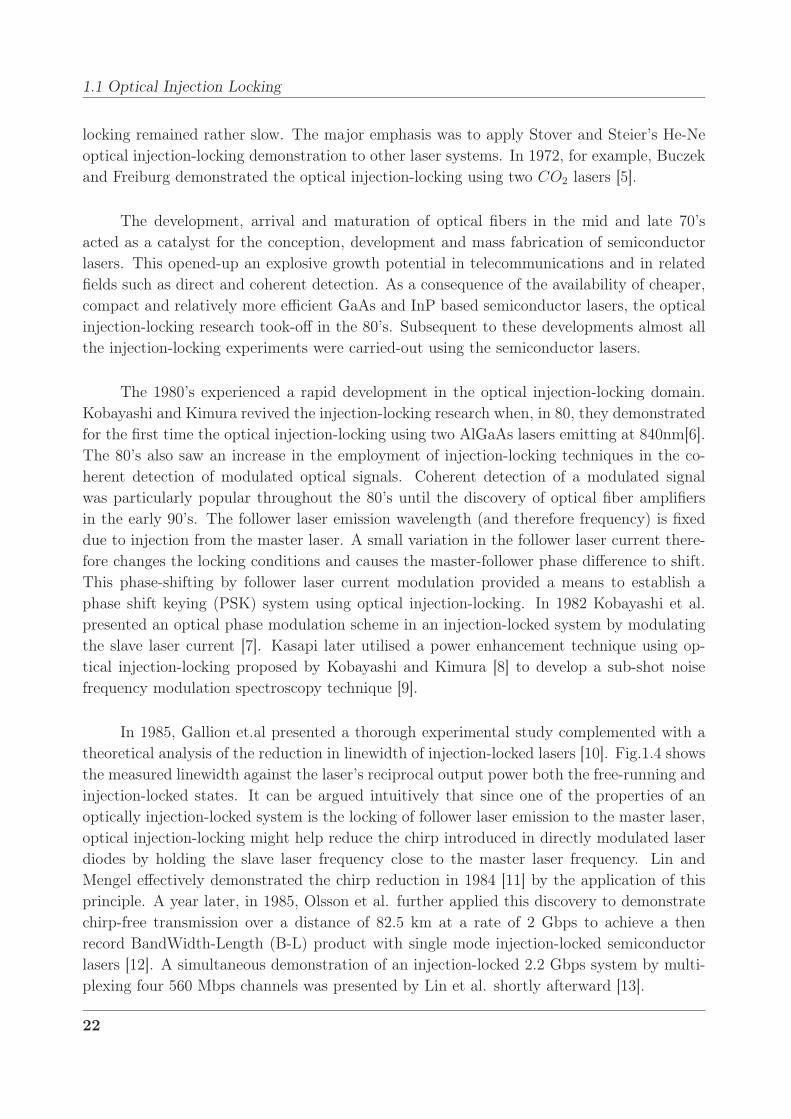
In 1985, Gallion et.al presented a thorough experimental study complemented with a
theoretical analysis of the reduction in linewidth of injection-locked lasers [10]. Fig.1.4 shows
the measured linewidth against the laser’s reciprocal output power both the free-running and
injection-locked states. It can be argued intuitively that since one of the properties of an
optically injection-locked system is the locking of follower laser emission to the master laser,
optical injection-locking might help reduce the chirp introduced in directly modulated laser
diodes by holding the slave laser frequency close to the master laser frequency. Lin and
Mengel effectively demonstrated the chirp reduction in 1984 [11] by the application of this
principle. A year later, in 1985, Olsson et al. further applied this discovery to demonstrate
chirp-free transmission over a distance of 82.5 km at a rate of 2 Gbps to achieve a then
record BandWidth-Length (B-L) product with single mode injection-locked semiconductor
lasers [12]. A simultaneous demonstration of an injection-locked 2.2 Gbps system by multi-
plexing four 560 Mbps channels was presented by Lin et al. shortly afterward [13].
22

Chapter 1 : Long Wavelength VCSEL Optical Injection-Locking
40
30
20
10
00.1 0.2 0.3 0.4 0.5 0.6
(mW-1)P-1m
Lin
ewid
th (
MH
z)
Pf-1
(mW-1)
(i)(ii)(iii)
Figure 1.4: (i) Free-running follower linewidth against its reciprocal output power P−1
f (ii) Master linewidth
against its reciprocal output power P−1m (iii) Injection-locked follower linewidth against reciprocal output
power P−1m [10].
The major theoretical works in the optical injection-locking domain were published in
the 1980’s as the above mentioned applications were developed. In 1982, Lang published his
landmark paper that detailed the locking properties of semiconductor lasers [14]. Lang was
the first to notice that the follower laser refractive index was subject to variations due to
injection of external optical power.
The techniques to calculate the locking range for microwave oscillators were already
published by several scientists, such as Kurokawa [15] 1973, but Lang was the first one to
demonstrate the inherent asymmetry in the locking range of a semiconductor laser based
optical injection-locking system. He argued that since the follower laser refractive index un-
dergoes a non-negligible change following the optical power injection from the master laser,
the locking range must depend upon the refractive index variation and the subsequent phase-
amplitude coupling.
In 1985, Henry neatly formulated Lang’s theory in his now famous paper by introducing
the linewidth enhancement factor, currently known as Henry’s factor, in the locking range
calculations[16]. He also extended the conventional two-equation model used to simulate
semiconductor laser small signal behavior to a three-equation model. The third equation
taking into account the phase perturbations due to the injection of external optical power.
23

1.1 Optical Injection Locking
Henry determined the mathematical relationship explaining the increase in resonance fre-
quency of an injection-locked laser but he concentrated more on the physical factors governing
the determination of locking range and the stability of an injection-locked system than fur-
ther exploring the bandwidth enhancement related to optical injection-locking. Mogensen
et al. [17] published several works in the same period presenting the injection-locked system
rate equations with Langevin noise sources. They also calculated the maximum phase tuning
limits of a master-follower system.
After a burst in research efforts on optical injection-locking in the 80’s, a rather slow pe-
riod was encountered in the early and mid 90’s. The reason for this can be explained with the
advent of erbium-doped fiber amplifiers (EDFAs). Most of the injection-locking applications
until then were focused on developing better ways to detect a modulated signal coherently.
The EDFA made the possibility of in-fiber optical amplification a reality and brought the
direct detection schemes to the foreground. Consequently optical injection-locking found it-
self a minor player in the booming telecoms revolution which was led principally by external
light modulators, high-speed photodiodes and optical fiber amplifiers.
This situation started changing in mid to late 90’s when first Simpson [18] and then
Meng et al. [19] demonstrated the increase in modulation bandwidths and resonance frequen-
cies of optically injection-locked semiconductor lasers. It was believed that injection-locking
along with the bandwidth enhancement, chirp reduction and linewidth improvement could
act as a major driving factor in the development of directly modulated long-haul high bit
rate telecommunication systems: But this was not to be. In fact the utilization of EDFAs
and external modulators had brought into market extremely reliable long-haul telecommu-
nication systems functioning at high bit rates. The deployment of external modulators (e.g.
of the Mach-Zhender type) not only avoided the chirp and linewidth related problems but
also helped to achieve very high modulation rates by gaining independence from the intrinsic
laser cavity parameters. The emergence of such an apparatus that achieved all the benefits
proposed by the injection-locking techniques without actually using two lasers and the rele-
vant circuitry made the optical injection-locking redundant. It is for this reason that since
late 90’s almost no further interest has been shown in the optical injection-locking of lasers
for long-haul telecommunication systems.
With the advances in long-haul telecommunication due to the emergence of optical
fibers, semiconductor lasers, photodiodes and fiber amplifiers, a vast optical fiber based in-
frastructure was laid out and developed through out the world especially in the Western
European countries, in the United States and Canada and in the Asian economic power-
houses such as Japan, South Korea, Hong Kong and Singapore. A powerful optical fiber
backbone system replaced the intercontinental submarine cables so much so that radio and
satellite communications were effectively evicted from the consumer telecommunication do-
main and started serving either as a backup or in proprietary applications.
24

Chapter 1 : Long Wavelength VCSEL Optical Injection-Locking
-8dBm-4dBm
-2dBm
Free-Running
0
-10
-20
-30
-40
-50
-600 5 10 15 20 25
Rel
ativ
e R
espo
nse
Modulation Frequency (GHz)
Figure 1.5: Demonstration of frequency response improvement of an injection-locked laser with increasing
injected optical power by Meng et. al [19].
It might sound a bit strange but the optical fiber led high bit rate telecommunication
revolution came to an abrupt end and by the first few years of the 21st century the optical
fiber based communications market was saturated. The reason was that once the optical
fiber based backbone networks were laid out, the telecommunication companies realized that
an optical fiber link to the subscriber would be utterly unfeasible economically due to very
high costs of the electro-optic equipment such as lasers, photodiodes and related circuitry
required for every subscriber. Optical fiber based telecommunication had economic utility
only over very large distances and very high bit rates such as Wide Area Networks (WANs),
Metropolitans Area Network (MANs) or inter continental links.
The economic bottleneck that halted the growth of optical fiber based communica-
tions posed a very challenging (and somewhat embarrassing) problem to researchers and
developers. The absence of Fiber To The Subscriber (FTTX) networks decreed that the
consumer remain on a copper-based or wireless systems (in fact POTS: Plain Old Tele-
phone System). Despite the giant leaps in optical fiber communications the Metropolitan
Area Networks (MANs) and the Local Area Networks (LANs) continued to operate using
electrical-electrical infrastructures and interfaces. This meant that despite the ability of
optical fiber based telecommunication networks to allow very high bit rates, the end-user
continued to suffer the meager bandwidths offered by the copper based systems. Attempts
were made to conceive high speed LANs using optical fibers but the cost of coherent light
sources always remained an insurmountable factor. The high cost of coherent light sources
for short-haul communications always translated into economic unfeasibility and underuti-
lization of the telecommunication system. Light Emitting Diodes (LEDs) were used in some
such optical fiber based LANs albeit more for want of anything suitable than as a conscious
25
1.2 Emergence of Vertical-Cavity Lasers
choice.
It is clear that the FTTX project needed a cheap, low-power, coherent light source,
compatible with the existing optical fiber infrastructure. The absence of such a source
translated into the continued utilization of older, low bit rate communication schemes and
infrastructures by the end-user.
1.2 Emergence of Vertical-Cavity Lasers
1.2.1 Historical Background and Motivation
It must be noted that the Vertical-Cavity Surface-Emitting Lasers (VCSELs) or simply
SELs (Surface-Emitting Lasers, as they were referred to as at that time) were not proposed
to overcome the bottlenecks that had hindered the progress of FTTX systems. The lasers
usually used for long-haul telecommunications have cleaved structures with edge emission.
Consequently they are referred to as Edge Emitting Lasers (EELs). This structure does
pose some problems, e.g. the initial probe testing of these devices is impossible before there
separation into individual chips. Their monolithic integration is also limited due to finite
cavity length. The cavity length implies generation of undesirable longitudinal modes and
the non-monolithic fabrication process implies the impossibility of fabricating laser arrays
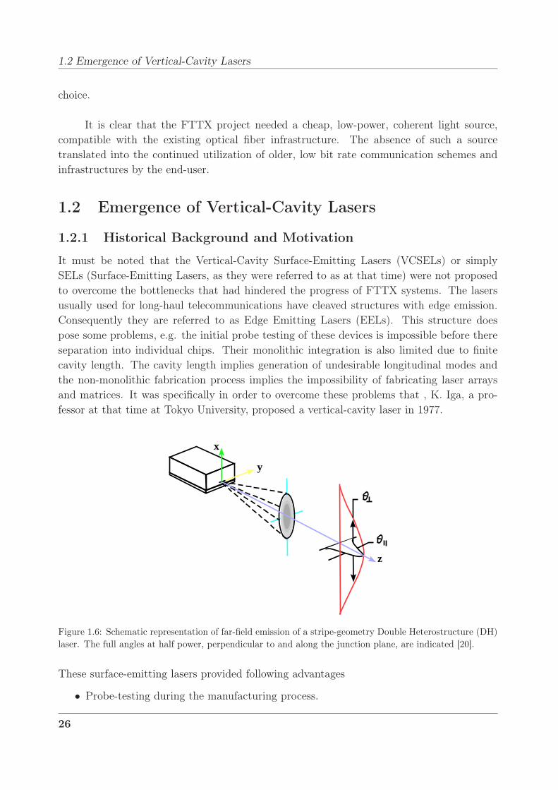
and matrices. It was specifically in order to overcome these problems that , K. Iga, a pro-
fessor at that time at Tokyo University, proposed a vertical-cavity laser in 1977.
x
y
z
Figure 1.6: Schematic representation of far-field emission of a stripe-geometry Double Heterostructure (DH)
laser. The full angles at half power, perpendicular to and along the junction plane, are indicated [20].
These surface-emitting lasers provided following advantages
• Probe-testing during the manufacturing process.
26
Chapter 1 : Long Wavelength VCSEL Optical Injection-Locking
• Fabrication of a large number of devices by fully monolithic processes yielding a very
low-cost chip-production.
• Very small cavity length guaranteeing longitudinal single mode operation.
• Possibility of production as arrays and matrices.
• Very low threshold currents due to ultra small cavity volume.
• Monolithic integration compatibility with other devices.
• Circular far-field pattern as compared to elliptical pattern for EELs.
A pulsed operation at 77K with a threshold current of 900mA was demonstrated in 1979
with a GaInAsP -InP vertical-cavity laser emitting at 1.3µm [21]. However, more pressing
issues regarding the delivery of higher bit rates using the conventional EELs meant that the
research into vertical-cavity lasers progressed very slowly. Consequently VCSEL research
and development stagnated through out the decade that followed its first demonstration.
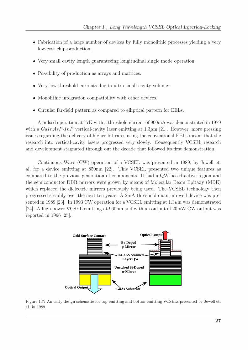
Continuous Wave (CW) operation of a VCSEL was presented in 1989, by Jewell et.
al, for a device emitting at 850nm [22]. This VCSEL presented two unique features as
compared to the previous generation of components. It had a QW-based active region and
the semiconductor DBR mirrors were grown by means of Molecular Beam Epitaxy (MBE)
which replaced the dielectric mirrors previously being used. The VCSEL technology then
progressed steadily over the next ten years. A 2mA threshold quantum-well device was pre-
sented in 1989 [23]. In 1993 CW operation for a VCSEL emitting at 1.3µm was demonstrated
[24]. A high power VCSEL emitting at 960nm and with an output of 20mW CW output was
reported in 1996 [25].
Gold Surface Contact
Be-Doped p-Mirror
InGaAS Strained Layer QW
Unetched Si-Doped n-Mirror
GaAs Substrate
Optical Output
Optical Output
Figure 1.7: An early design schematic for top-emitting and botton-emitting VCSELs presented by Jewell et.
al. in 1989.
27
1.2 Emergence of Vertical-Cavity Lasers
The polarisation properties of VCSELs emitting in the near infra-red ranges were inves-
tigated, for the first time, by Besnard et. al in 1996 [26], [27]. It wasšshown that commercial
VCSELs’ emission switches between two eigenstates with the injection of polarized light
inside the VCSEL optical cavity. This technique could then be utilised for switching appli-
cations in telecommunication networks. Bondiou et. al demonstrated the push-pull effects,
hysteresis phenomena, chaos and phase and frequenct-locking using injection-locking in long
wavelength single-mode VCSELs [28].
Despite these advances and maturity in fabrication technology, the VCSELs could not
replace the EELs as optical sources for long-haul telecommunications and were hence con-
fined to other applications such as optical computing, sensors, barcode scanners and data
storage etc.
The reason for this shortcoming lies in the VCSEL physical structure that gives priority
to
• Monolithic integration favoring vertical emission
• Low threshold current
• On chip testing
These priorities impose a set of design guidelines for VCSEL fabrication which, when
implemented, induce certain unwanted and unforeseen traits in the device behavior. These
undesirable characteristics rendered the VCSEL unsuitable for utilization in prevalent telecom-
munication systems.
Following is a concise analysis of these shortcomings. We would present the basic
VCSEL structure that would try to achieve the above given objectives. Following this dis-
cussion we would present the drawbacks in the device performance related to the realization
of design objectives. Certain remedies and improvements would then be presented in order
to render the device more performing and efficient.
1.2.2 VCSEL Structure
A VCSEL is essentially a gain medium based active region vertically stacked between two
Distributed Bragg Reflectors (DBRs). In order to achieve a single mode operation it is pro-
posed that the length of the active region be very small: Effectively of the order of the desired
lasing wavelength. A short cavity eliminates the generation of longitudinal modes associated
to Fabry-Perot cavities. This however imposes a severe restriction on VCSEL DBR design.
The threshold gains for the surface-emitting and edge-emitting devices must be comparable
regardless of the cavity length. The threshold gain of an EEL is approximately 100cm−1.
28
Chapter 1 : Long Wavelength VCSEL Optical Injection-Locking
For a VCSEL of active layer thickness of 0.1 µm, this value corresponds to a single-pass gain
of about 1%. Thus for a VCSEL to lase with a threshold current density comparable to that
of an EEL, the mirror reflectivities must be greater than 99% in order to ensure that the
available gain exceeds the cavity losses during a single-pass.
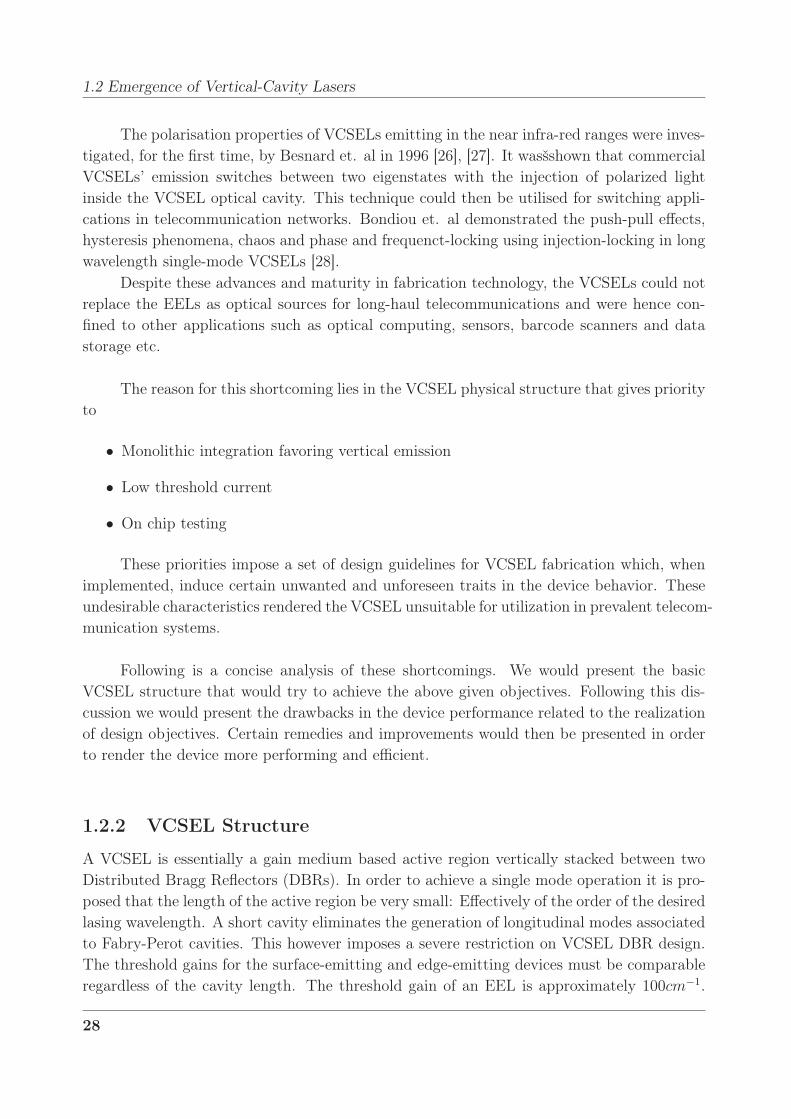
Achieving a reflectivity of 99% with DBRs is a formidable task and thus central to the
conception of low threshold VCSELs is the capacity to fabricate high reflectivity mirrors.
Let’s consider the example of a VCSEL operating at 850nm. The active region would consist
of several ultra thin layers composed alternately of GaAs and AlGaAs materials. The differ-
ence between the refractive index of layers of a pair determines the number of pairs required
to achieve a reflectivity of 99% or more. In the case of AlAs-Al0.1Ga0.9As the refractive index
difference between two alternate layers is 0.6 (cf. Fig.1.8) [29]. Consequently, as shown in
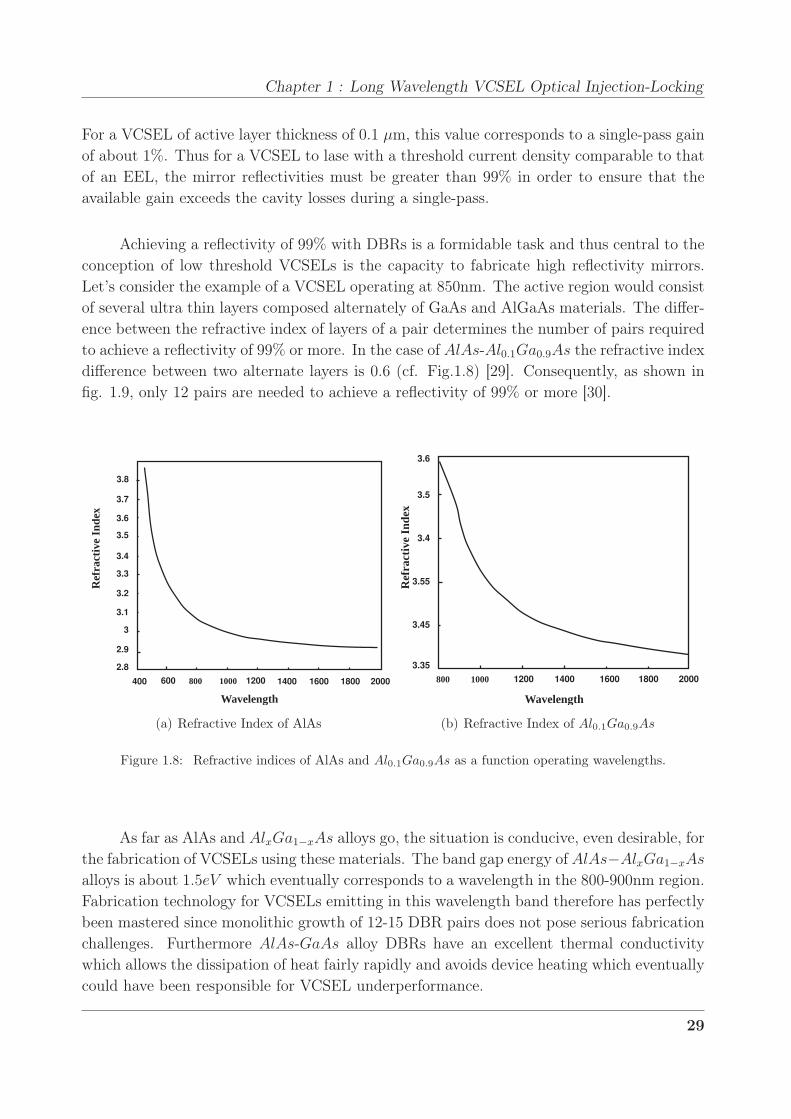
fig. 1.9, only 12 pairs are needed to achieve a reflectivity of 99% or more [30].
400 600 1200 1400 1600 1800 2000
3.7
3.6
3.5
3.4
3.3
3.2
3.1
3
2.9
2.8
Ref
ract
ive
Inde
x
Wavelength
3.8
800 1000
(a) Refractive Index of AlAs
1200 1400 1600 1800 2000
3.6
3.5
3.4
3.55
3.45
3.35
Ref
ract
ive
Inde
x
Wavelength
800 1000
(b) Refractive Index of Al0.1Ga0.9As
Figure 1.8: Refractive indices of AlAs and Al0.1Ga0.9As as a function operating wavelengths.
As far as AlAs and AlxGa1−xAs alloys go, the situation is conducive, even desirable, for
the fabrication of VCSELs using these materials. The band gap energy of AlAs−AlxGa1−xAs
alloys is about 1.5eV which eventually corresponds to a wavelength in the 800-900nm region.
Fabrication technology for VCSELs emitting in this wavelength band therefore has perfectly
been mastered since monolithic growth of 12-15 DBR pairs does not pose serious fabrication
challenges. Furthermore AlAs-GaAs alloy DBRs have an excellent thermal conductivity
which allows the dissipation of heat fairly rapidly and avoids device heating which eventually
could have been responsible for VCSEL underperformance.
29
1.2 Emergence of Vertical-Cavity Lasers
8 10 12 14 16 18 20
100
99.5
99
98.5
98
97.5
97
96.5
96
95.5
95
Ref
lect
ivit
y
Number of Pairs
Figure 1.9: Calculated reflectivity of an AlAs-Al0.1Ga0.9As multilayer semiconductor Bragg reflector as a
function of the number of pairs [30].
1.2.3 Performance Drawbacks
As far as the fabrication of near infrared VCSELs was concerned, the existing technologies
and fabrication processes proved to be quite adequate. However, applying a similar method-
ology to telecommunication wavelength VCSELs proved to be much more challenging. Long
wavelength VCSELs operating in the 1.1µm-1.6µm range are of considerable interest for
optical fiber telecommunications since the hydroxyl absorption and pulse dispersion nulls
for silicon optical fibers are found at 1.5µm and 1.3µm respectively. Although several ma-
terial systems were considered, the combination InGaAsP -InP turned out to be the most
suitable in view of the near perfect lattice match. The active layer is composed of the
In1−xGaxAsyP1−y quaternary alloy. By varying mole fractions x and y, almost any wave-
length within the 1.1−1.6µm can be selected.
1.2.3.1 DBR Growth
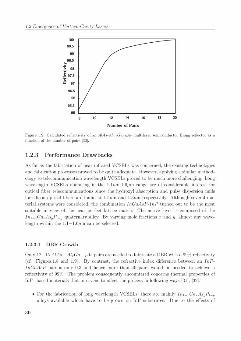
Only 12−15 AlAs−AlxGa1−xAs pairs are needed to fabricate a DBR with a 99% reflectivity
(cf. Figures.1.8 and 1.9). By contrast, the refractive index difference between an InP -
InGaAsP pair is only 0.3 and hence more than 40 pairs would be needed to achieve a
reflectivity of 99%. The problem consequently encountered concerns thermal properties of
InP−based materials that intervene to affect the process in following ways [31], [32]:
• For the fabrication of long wavelength VCSELs, there are mainly In1−xGaxAsyP1−y
alloys available which have to be grown on InP substrates. Due to the effects of
30
Chapter 1 : Long Wavelength VCSEL Optical Injection-Locking
non negligible Auger’s recombination effects and intravalence band absorption, these
materials suffer from temperature-dependent losses.
• The thermal conductivity is greatly reduced due to alloy disorders which causes phonon
scattering. This reduction in thermal conductivity is particularly adverse for effective
heat sinking through the VCSELs’ DBRs usually having a thickness of several µms.
• AlAs-AlxGa1−xAs DBRs have a good thermal conductivity and could be thinner but
due to lattice mismatch could not be grown on the InP substrate.
DBR growth has been one of the fundamental problems regarding the fabrication of long
wavelength VCSELs that has hampered the entry of VCSELs in high-speed data, command
and telecommunications domain.
AlAs (0.91)
GaAs 0.44 InAs
(0.27)
Lattice-Matched alloys (0.042)
LatticeConstant (nm)
Band-gap (eV)
Th
erm
al C
ond
uct
ivit
y (W
/(cm
K))
2.7
2.21.7
1.2
0.7
0.2 0.560.57
0.580.59
0.610.60
InP
Figure 1.10: Thermal conductivity of the various alloy compositions of the InGaAlAs Material System
plotted versus free lattice constant and band gap energy. The line indicates the quaternary compositions
that can be used for DBRs on InP. [32]
It can be seen in the Fig.1.10 that the values of thermal conductivity for InP−based
materials lattice matched alloys are very feeble as compared to those of GaAs, AlAs or InAs
alloys.
1.2.3.2 Optical and Electrical Confinement
Growing stacks of DBRs was not the only problem encountered by VCSEL manufacturers.
One of the primary objectives of VCSEL design was to fabricate short cavity single mode
devices. The short cavity did eliminate the undesirable longitudinal modes but it gave birth
to another unforeseen problem. Initial VCSEL designs suggested that the carriers and the
photons share a common path traversing the DBRs. This led to the heating of certain zones
31
1.2 Emergence of Vertical-Cavity Lasers
of the DBRs due to carrier flow and resulted in a variable refractive index distribution inside
the VCSEL optical cavity. This phenomenon is known as “Thermal Lensing”. Instead of
being concentrated in the center in the form of a single transverse mode, the optical energy
is repartitioned azimuthally inside the optical cavity. This particular optical energy distri-
bution is observed in the form of transverse modes. Higher bias currents therefore imply
high optical power and in consequence a higher number of transverse modes.
An oxide-aperture is employed, principally in shorter wavelength emission VCSELs, in
order to block the unwanted transverse modes. The oxide-aperture diameter then determines
the multimode or single mode character of a VCSEL. VCSELs having oxide aperture diam-
eters greater than 5µm exhibit multimode behavior. It can also be inferred from the above
discussion that for the type of VCSELs employing the oxide-aperture technology for optical
confinement, single mode VCSELs almost always have emission powers less than those of
multimode VCSELs.
The problem of optical and electrical confinement are hence interrelated. It is evident
that in order to attain single mode emission the thermal lens effect must be avoided. This
can only be achieved by segregating the carrier and photon paths. Although challenging
technically, it can be achieved using a tunnel junction. The concept and functioning of a
tunnel junction is explained in the following sub-section.
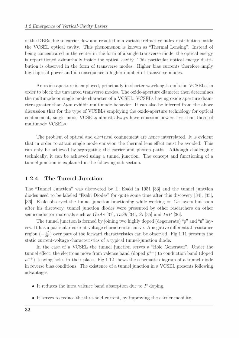
1.2.4 The Tunnel Junction
The “Tunnel Junction” was discovered by L. Esaki in 1951 [33] and the tunnel junction
diodes used to be labeled “Esaki Diodes” for quite some time after this discovery [34], [35],
[36]. Esaki observed the tunnel junction functioning while working on Ge layers but soon
after his discovery, tunnel junction diodes were presented by other researchers on other
semiconductor materials such as GaAs [37], InSb [34], Si [35] and InP [36].
The tunnel junction is formed by joining two highly doped (degenerate) “p” and “n” lay-
ers. It has a particular current-voltage characteristic curve. A negative differential resistance
region (− dIdV
) over part of the forward characteristics can be observed. Fig.1.11 presents the
static current-voltage characteristics of a typical tunnel-junction diode.
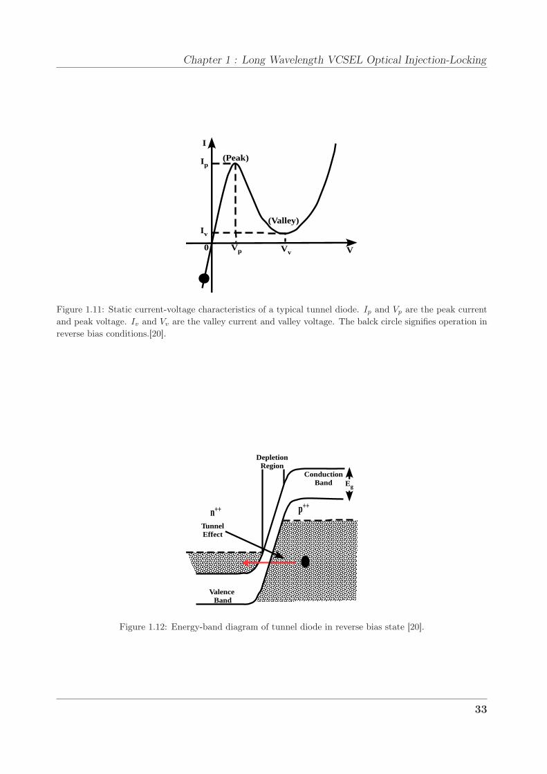
In the case of a VCSEL the tunnel junction serves a “Hole Generator”. Under the
tunnel effect, the electrons move from valence band (doped p++) to conduction band (doped
n++), leaving holes in their place. Fig.1.12 shows the schematic diagram of a tunnel diode
in reverse bias conditions. The existence of a tunnel junction in a VCSEL presents following
advantages:
• It reduces the intra valence band absorption due to P doping.
• It serves to reduce the threshold current, by improving the carrier mobility.
32
Chapter 1 : Long Wavelength VCSEL Optical Injection-Locking
(Peak)
(Valley)
V
I
Ip
Iv
Vp Vv0
Figure 1.11: Static current-voltage characteristics of a typical tunnel diode. Ip and Vp are the peak current
and peak voltage. Iv and Vv are the valley current and valley voltage. The balck circle signifies operation in
reverse bias conditions.[20].
p++n++
Conduction Band
Valence Band
Eg
Depletion Region
Tunnel Effect
Figure 1.12: Energy-band diagram of tunnel diode in reverse bias state [20].
33

1.2 Emergence of Vertical-Cavity Lasers
• It is used for electrical as well as optical confinement.
Due to these properties, the tunnel junction has become an integral part of long wave-
length VCSELs.
1.2.5 Technological Breakthroughs and Advances in Long Wave-
length VCSEL Fabrication
Although by the start of the 21st century serial production and delivery of VCSELs was in
full flow for diverse applications, they had failed to fulfill the two following essential criteria
for utilization in optical networks.
• They did not emit in the 1.3µm and 1.5µm range: The so-called “Telecoms Wave-
lengths”. This meant not only definition and standardization of new standards at
850nm wavelength but also the deployment and manufacturing of a host of optical
components such as optical fibers, couplers, multiplexers and photodiodes compatible
with the 850nm emission range.
• As has been explained above, transverse-mode operation starts to manifest itself from
a few milliamperes above the threshold current rendering the VCSELs multimode in
character. This multimodality is disconcerting in two ways:
– It reduces the effective channel bandwidth hence reducing the maximum deliver-
able bit rate.
– It requires the utilization of multimode optical fiber which although being less
expensive than the single mode fiber, affects the VCSEL operation in another way.
When high optical powers are injected in a multimode fiber, several undesired fiber
modes are excited thus reducing the effective bandwidth.
It is clear from the above discussion that a suitable substitute for EELs, for applications
in short to medium distance optical fiber networks, must possess the following properties
• It must emit at either 1.3µm or at 1.5µm wavelength so that the existing standards,
infrastructure, optoelectronic components and devices could be utilized.
• It must have a single mode emission spectrum so as to profit from the high bandwidths
offered by the employment of single mode optical fibers.
As late as 2000, there were no serial production and mass deployment of VCSELs
that fulfilled these two essential criteria. As has been discussed above, this was due to the
technical challenges posed by a combination of several different factors which rendered the
fabrication of long wavelength VCSEL devices very difficult.
34
Chapter 1 : Long Wavelength VCSEL Optical Injection-Locking
1.3 Emergence of Long Wavelength VCSELs
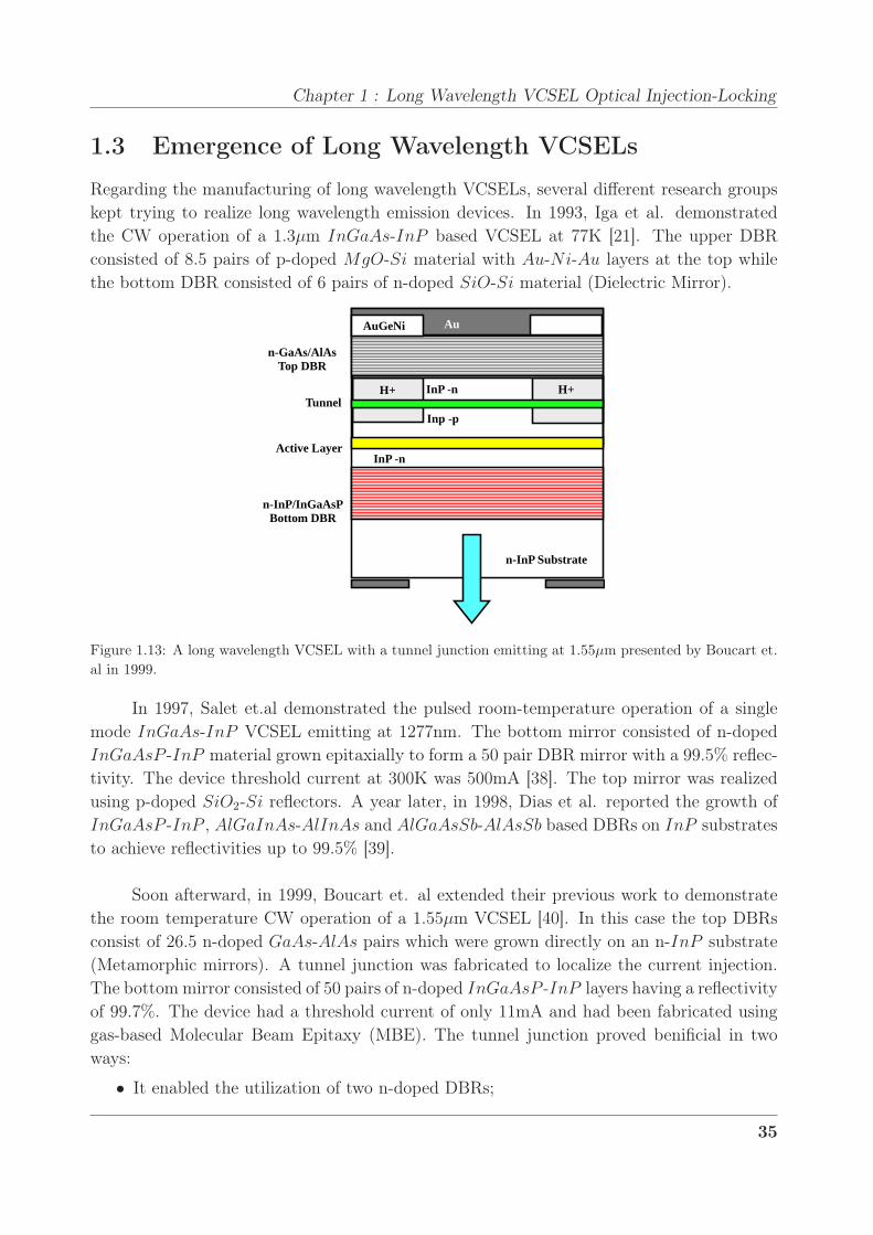
Regarding the manufacturing of long wavelength VCSELs, several different research groups
kept trying to realize long wavelength emission devices. In 1993, Iga et al. demonstrated
the CW operation of a 1.3µm InGaAs-InP based VCSEL at 77K [21]. The upper DBR
consisted of 8.5 pairs of p-doped MgO-Si material with Au-Ni-Au layers at the top while
the bottom DBR consisted of 6 pairs of n-doped SiO-Si material (Dielectric Mirror).
n-InP Substrate
Active Layer
n-InP/InGaAsP Bottom DBR
H+ H+
AuGeNi
InP -n
Inp -pTunnel
n-GaAs/AlAs Top DBR
Au
InP -n
Figure 1.13: A long wavelength VCSEL with a tunnel junction emitting at 1.55µm presented by Boucart et.
al in 1999.
In 1997, Salet et.al demonstrated the pulsed room-temperature operation of a single
mode InGaAs-InP VCSEL emitting at 1277nm. The bottom mirror consisted of n-doped
InGaAsP -InP material grown epitaxially to form a 50 pair DBR mirror with a 99.5% reflec-
tivity. The device threshold current at 300K was 500mA [38]. The top mirror was realized
using p-doped SiO2-Si reflectors. A year later, in 1998, Dias et al. reported the growth of
InGaAsP -InP , AlGaInAs-AlInAs and AlGaAsSb-AlAsSb based DBRs on InP substrates
to achieve reflectivities up to 99.5% [39].
Soon afterward, in 1999, Boucart et. al extended their previous work to demonstrate
the room temperature CW operation of a 1.55µm VCSEL [40]. In this case the top DBRs
consist of 26.5 n-doped GaAs-AlAs pairs which were grown directly on an n-InP substrate
(Metamorphic mirrors). A tunnel junction was fabricated to localize the current injection.
The bottom mirror consisted of 50 pairs of n-doped InGaAsP -InP layers having a reflectivity
of 99.7%. The device had a threshold current of only 11mA and had been fabricated using
gas-based Molecular Beam Epitaxy (MBE). The tunnel junction proved benificial in two
ways:
• It enabled the utilization of two n-doped DBRs;
35

1.3 Emergence of Long Wavelength VCSELs
• Once the conductive properties of the tunnel junction were neutralized using H+ ion
implantation, it served to localize the current injection without having to etch a mesa.
The resulting device was therefore coplanar in structure
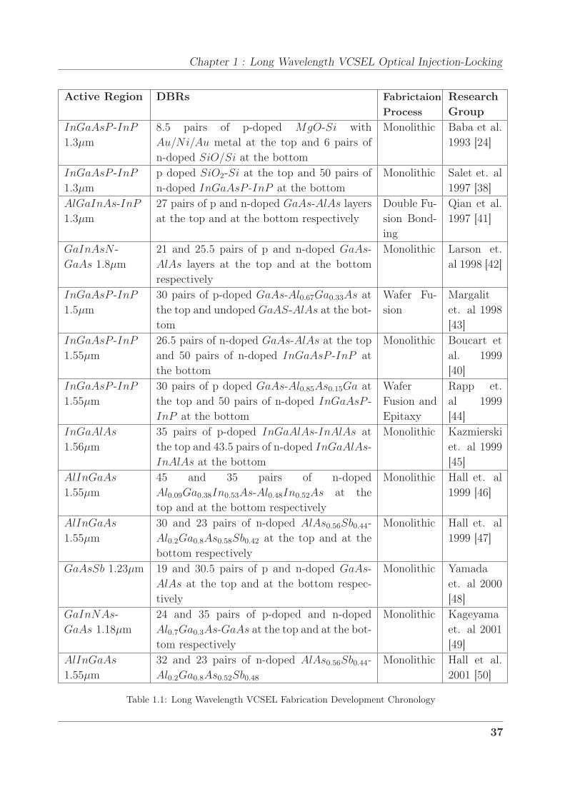
It can be ascertained from Table.1.1 that several different materials such as InGaAsP ,
InGaAsAl, InGaAsSb and InGaAsN were chosen to fabricate the active layer. The mate-
rial choice for DBRs and the fabrication processes were equally diverse. Although most of the
research groups chose “Monolithic Integration Techniques” for the fabrication of VCSELs,
“Wafer Fusion” , and “Fusion Bonding” were also applied.
Meanwhile, in 1998, the Institute of Electrical and Electronics Engineers (IEEE) defined
the “1000BASEX-Gbps Ethernet over Fiber-Optic at 1Gbit/s” standard. This standard for
the transmission of “Ethernet Frames” at a rate of at least one Gbps was defined using light
sources emitting at 850nm. The definition of Gigabit Ethernet standards using 850nm optical
sources boosted the research and development of near infrared emission VCSELs. By the year
2000, 850nm VCSELs had firmly established themselves as standard optical sources for short-
haul communication applications. This development was a setback for ongoing research in
long wavelength VCSELs and as a result many research groups shifted their focus from long
wavelength VCSEL development to other emerging fields. Furthermore, the research focus,
even in the long wavelength VCSEL development field, shifted toward a new dimension. Long
wavelength VCSELs were no longer being developed solely as telecommunication sources,
an emerging field of spectroscopy was beginning to play an increasingly important part in
eventual long wavelength VCSEL applications.
1.3.1 Vertilas VCSELs
Although long wavelength VCSEL operation using a tunnel junction device was already
demonstrated by Boucart et al. [40] in 1999, Ortsiefer et al. [51] presented a variation to
this concept. Soon the single mode room temperature operation of an InP-based VCSEL
Isolation
Electroplated Gold Heat Sink
Bottom Dielectric Mirror Active Region
BTJ
n-side Contact
p-side Contact
Top DBR
Optical Output
Figure 1.14: A Vertilas BTJ structure with an emission wavelength of 1.55µm [31].
operating at 1.5µm was demonstrated by the same research group [52]. The top DBR is
36
Chapter 1 : Long Wavelength VCSEL Optical Injection-Locking
Active Region DBRs Fabrictaion
Process
Research
Group
InGaAsP -InP
1.3µm
8.5 pairs of p-doped MgO-Si with
Au/Ni/Au metal at the top and 6 pairs of
n-doped SiO/Si at the bottom
Monolithic Baba et al.
1993 [24]
InGaAsP -InP
1.3µm
p doped SiO2-Si at the top and 50 pairs of
n-doped InGaAsP -InP at the bottom
Monolithic Salet et. al
1997 [38]
AlGaInAs-InP
1.3µm
27 pairs of p and n-doped GaAs-AlAs layers
at the top and at the bottom respectively
Double Fu-
sion Bond-
ing
Qian et al.
1997 [41]
GaInAsN -
GaAs 1.8µm
21 and 25.5 pairs of p and n-doped GaAs-
AlAs layers at the top and at the bottom
respectively
Monolithic Larson et.
al 1998 [42]
InGaAsP -InP
1.5µm
30 pairs of p-doped GaAs-Al0.67Ga0.33As at
the top and undoped GaAS-AlAs at the bot-
tom
Wafer Fu-
sion
Margalit
et. al 1998
[43]
InGaAsP -InP
1.55µm
26.5 pairs of n-doped GaAs-AlAs at the top
and 50 pairs of n-doped InGaAsP -InP at
the bottom
Monolithic Boucart et
al. 1999
[40]
InGaAsP -InP
1.55µm
30 pairs of p doped GaAs-Al0.85As0.15Ga at
the top and 50 pairs of n-doped InGaAsP -
InP at the bottom
Wafer
Fusion and
Epitaxy
Rapp et.
al 1999
[44]
InGaAlAs
1.56µm
35 pairs of p-doped InGaAlAs-InAlAs at
the top and 43.5 pairs of n-doped InGaAlAs-
InAlAs at the bottom
Monolithic Kazmierski
et. al 1999
[45]
AlInGaAs
1.55µm
45 and 35 pairs of n-doped
Al0.09Ga0.38In0.53As-Al0.48In0.52As at the
top and at the bottom respectively
Monolithic Hall et. al
1999 [46]
AlInGaAs
1.55µm
30 and 23 pairs of n-doped AlAs0.56Sb0.44-
Al0.2Ga0.8As0.58Sb0.42 at the top and at the
bottom respectively
Monolithic Hall et. al
1999 [47]
GaAsSb 1.23µm 19 and 30.5 pairs of p and n-doped GaAs-
AlAs at the top and at the bottom respec-
tively
Monolithic Yamada
et. al 2000
[48]
GaInNAs-
GaAs 1.18µm
24 and 35 pairs of p-doped and n-doped
Al0.7Ga0.3As-GaAs at the top and at the bot-
tom respectively
Monolithic Kageyama
et. al 2001
[49]
AlInGaAs
1.55µm
32 and 23 pairs of n-doped AlAs0.56Sb0.44-
Al0.2Ga0.8As0.52Sb0.48
Monolithic Hall et al.
2001 [50]
Table 1.1: Long Wavelength VCSEL Fabrication Development Chronology
37

1.3 Emergence of Long Wavelength VCSELs
composed of 34.5 InGaAlAs-InAlAs pairs. The bottom mirror is comprised of 2.5 pairs
of CaF2-Si with Au-coating. The gold coating, apart from serving as a high reflectivity
mirror (99.75%), serves as an integrated heat sink [31]. The successful incorporation of tun-
nel junction in the long wavelength VCSEL design proved to be the technical breakthrough
that would present VCSELs as standard devices for short to medium distance optical fiber
communications. By 2002 Vertilas was delivering 1.55µm single mode VCSELs for 10Gbps
operation.
1.3.2 BeamExpress VCSELs
1.3.2.1 Wafer Fusion
The manufacturing of a long wavelength VCSEL requires the growth of an InP -InGaAsP
alloy active region on an InP substrate. These alloys however are difficult to grow as DBR
stacks above and below the active region since the restrictions imposed by the material ther-
mal conductivity render proper device functioning impossible. On the other hand, AlAs-
AlxGa1−xAs DBRs have a good thermal conductivity but they can not be monolithically
grown on InP -based substrates due to lattice mismatch. The solution to the matching of
disparate materials to optimize VCSEL performance was developed at the University of Cal-
ifornia Santa Barbara (UCSB) in 1996 by Margalit et. al [53].
The technique utilized is known as “Wafer Fusion” or “Wafer Bonding” and consists of
establishing chemical bonds directly between two materials at their hetero-interface in the
absence of an intermediate layer [54]. The first demonstration constituted of fabrication of
a 1.55µm VCSEL. The device was fabricated by wafer fusion of MOVPE-grown InGaAsP
quantum well active region to two MBE-grown AlGaAs-GaAs DBR reflectors [53].
1.3.2.2 Localized Wafer Fusion
By applying a variant of the “Wafer Fusion” technique in 2004, Kapon et. al demonstrated
that it was possible to grow separate components of a VCSEL cavity on separate host
substrates [55], [56]. These separate components were then bonded (fused) together to
construct the complete VCSEL optical cavity. This process was developed at the Ecole
Polytechnique Fédérale de Lausanne (EPFL) and patented as “Localized Wafer Fusion”.
A majority of VCSELs used in this work are BeamExpress VCSELs. Fig.1.15 presents
the structure of a BeamExpress VCSEL with an emission wavelength of 1.55µm. This is a
double intracavity contact single-mode VCSEL with coplanar access. The InP -based optical
cavity consists of five InAlGaAs quantum wells. The top and bottom DBRs comprise of
21 and 35 pairs respectively and are grown by Metal-Organic Chemical Vapor Deposition
(MOCVD) epitaxy method. Using the technique of localized wafer fusion, the top and the
38

Chapter 1 : Long Wavelength VCSEL Optical Injection-Locking
bottom AlGaAs-GaAs DBRs are then bonded to the active cavity wafer and the tunnel
junction mesa structures.
Using VCSELs with double intracavity contacts has its own advantages. These contacts
are much nearer to the active region than the classical contacts. Their utilization combined
with the presence of tunnel junction allows to have lower series resistance as compared to
oxidized-aperture VCSELs. Due to this proximity of the contacts to the active region these
VCSELs tend to have a high quantum efficiency. Their location near the active region results
in no current passage through DBRs.
AlGaAs-GaAs Top DBR
AlGaAs-GaAs Bottom DBR
Fusion InterfaceGaAs Substarte
MQW-based Active Region
Intravavity Contacts
Tunnel Junction
Figure 1.15: Schematic diagram of a wafer-fused Beam-Express VCSEL with an emission wavelength of
1.5µm.
The process used for the fabrication of Beam Express VCSELs is not monolithic. The
bottom AlGaAs-GaAS DBR is grown on the GaAs substrate. The InP -based cavity is
then bonded to this DBR. After the growth of an isolation layer on the active region, the
epitaxially grown AlGaAs-GaAs top DBR is fused to complete the optical cavity. This
double fusion increases the complexity of the fabrication process but it presents certain
advantages. Wafer-fusion allows to replace the InAlGaAs DBRs by GaAs DBRs. Not only
the GaAs DBRs have a better thermal conductivity, they are much cheaper than InAlGaAs
DBRs which allows to increase the performance and decrease the cost of the component at
the same time. The biggest advantage of “Wafer Fusion” is the possibility of serial production
of VCSELs which further serves to reduce the component cost.
1.3.3 RayCan VCSELs
Starting as a spin-off company from the Korean government funded Electronics and Telecom-
munications Research Institute (ETRI) in 2002, RayCan launched an ambitious project for
manufacturing of long wavelength VCSELs. Instead of using the above described specialized
technologies for long wavelength VCSEL manufacturing, RayCan decided to embark upon
a different course. They decided to monolithically grow InAlGaAs DBRs and an InGaAs-
based quantum well active region on an InP substrate. As has been discussed above, this
technique was previously not considered because in order to achieve 99% reflectivity using
InAlGaAs-based DBRs, a growth of more than 40 pairs is needed. Fig. 1.16 presents a
39

1.4 Long Wavelength VCSEL Direct Modulation
comparison of the number of DBRs needed to achieve a near unity reflectivity using different
materials.
1
0.5
0
GaAs/AlGaAs
InGaAsP/InP
AlInGaAs/AlInAs
AlGaAsSb/AlAsSb
10 20 30 40 50Number of Mirrors
Ref
lect
ivit
y
Figure 1.16: Calculated reflectivity of different materials used as semiconductor Bragg reflectors as a function
of the number of pairs [57].
RayCan employed Metal-Organic Chemical Vapor Deposition (MOCVD) technique to
fabricate a long wavelength VCSEL. For 1.55µm VCSELs, the top and bottom DBRs were
grown as 28 and 38 pairs of undoped InAlGaAs-InAlAs schemes. The top and bottom
DBRs consisted of 33 and 50 layers respectively for 1.3µm emission VCSELs. The 0.5λ thick
active region consists of seven pairs of strain-compensated (SC) InAlGaAs quantum wells
[58]. The lower number of top DBRs in both the VCSELs was compensated by using an
InAlGaAs phase-matching layer and Au metal layer. Figure. 3.20 presents the structure of
a RayCan VCSEL emitting at 1.5µm. RayCan has been shipping 1.3µm and 1.5µm VCSELs
since 2004. In November 2005 RayCan shipped its first 10GBit/s long wavelength CWDM
VCSEL module.
1.4 Long Wavelength VCSEL Direct Modulation
1.4.1 Need for VCSEL Optical Injection-Locking
Up to this point we have discussed the prospects of long wavelength VCSELs in the context
of high bit rate data delivery over medium and short distance links. It would not be an ex-
aggeration to state that consumer demand for multimedia and interactive applications and
therefore bandwidth has increased to an unprecedented level. Current electrical-electrical
infrastructures can not support this demand. The major obstacle in switching from elec-
trical/hertzian systems to optical/fibered systems is the cost of the coherent optical source
compatible with existing infrastructure. Recent advances in the fabrication, development
40

Chapter 1 : Long Wavelength VCSEL Optical Injection-Locking
DBR
DBR
N-InP
Bottom Electrode Top Electrode
AR Coating
Air Gap
InP Substrate
MQW Active Region
Tunnel Junction
SiNx
Figure 1.17: MOVCD Grown monolithic structure of a 1.5µm RayCan VCSEL.
and serial production of VCSELs emitting at 1.3µm and 1.5µm have paved the way for fu-
ture FTTX systems [59].
Having been able to solve the problem at component level, by developing reliable long
wavelength VCSELs, the next logical approach is the development of new systems incor-
porating these components. Conventionally the EELs used in the long-haul fiber links are
externally modulated i.e. the photon generation process inside the cavity is independent
of the modulation mechanism. While being extremely effective, this method necessitates
the utilization of an external modulator which increases the system cost. Such a scheme is
inherently unfeasible for FTTX systems due to the cost of the external modulators.
The elimination of external modulators as a component of choice for FTTX systems de-
crees the employment of direct modulation techniques. In this technique the laser diode bias
current is varied to achieve the optical output intensity variation. Apparently the scheme is
simple and easy to implement, but when put into practice, it presents two major problems
which are detailed in the following two sub-sections.
1.4.1.1 Phase-Amplitude Coupling
Semiconductor lasers, whether EELs or VCSELs, are different from other lasers in one re-
spect. The refractive index of a semiconductor laser depends on the carrier concentration
inside the cavity. The carrier concentration variation affects the refractive index of the cavity
which eventually changes the emission wavelength of the component. The consequences of
41

1.5 Long Wavelength VCSEL Optical Injection-Locking
this uniqueness manifest themselves during the process of direct modulation. A variation in
bias currents varies the optical output power as well as the optical frequency of the cavity.
These variations are proportional to the variation in carrier concentration and therefore the
bias current. The device is modulated in amplitude and frequency at the same time. This
phenomenon of “Phase-Amplitude Coupling” or the dynamic shift of the lasing frequency
during modulation is known as “Frequency Chirping” or simply “Chirping”.
Chirping broadens the linewidth of a laser. The extent to which a pulse broadens
depends upon the amplitude of the modulating signal. Larger modulation amplitudes result
in linewidths of the order of GHz 1. This spectral broadening at the time of modulation
becomes more pronounced during the passage of the modulated pulse through an optical
channel and the effective channel bandwidth is reduced. Direct modulation while being
cost-effective proves to be inefficient, in terms of deliverable bit rates, when compared to
external modulation.
1.4.1.2 Intrinsic Modulation Limits
A semiconductor optical cavity, in essence, is a resonator. Like every resonator, or electrical
circuit for that matter, its frequency response depends on its intrinsic parameters. In case of
semiconductor lasers these parameters might be cavity volume, photon and electron popula-
tions, group velocity, gain compression factor etc. When directly modulated, a laser can not
better the modulation frequency response already defined by these intrinsic parameters. On
the other hand, the utilization of an external modulator provides a means to bypass the laser
intrinsic parameters. The modulation response (or the deliverable bit rate) of the system is
then defined by the external modulator and not the laser.
1.5 Long Wavelength VCSEL Optical Injection-Locking
It is clear from the description of the two above given problems that a viable optical system
must minimize the effects of “Amplitude-Phase Coupling” and “Intrinsic Modulation Limits”
in order to be efficient and acceptable. Once injection-locked, the master laser holds the
frequency of the follower laser and makes it immune to carrier variations. This isolation
from carrier variations appears as the reduction of chirp during direct modulation. In 1984,
Lin et al. [11] demonstrated the reduction of frequency chirping in a directly modulated
semiconductor laser by the application of injection-locking technique.
Henry presented an approximate formula for the calculation of resonance frequency
of optically injection-locked semiconductor lasers [16] but its significance was not appreci-
ated at that time until Simpson [61] and Meng [62] demonstrated bandwidth and resonance
frequency enhancements in late 90’s. In 2002, a research group in University of California
1Typical VCSEL linewidth is of the order of tens of MHz [60].
42

Chapter 1 : Long Wavelength VCSEL Optical Injection-Locking
Berkley (UCB), led by Connie J. Chang-Hasnain reported the first optical injection-locking
of a long wavelength VCSEL for 2.5Gb/s transmission [63].
In 2003 long wavelength VCSEL chirp reduction and bandwidth enhancement were
presented by the same research group [64] but there was a marked technical difference from
their first publication. Whereas the first time optical injection-locking of a long wavelength
VCSEL was carried-out using an identical VCSEL, the second demonstration used a Dis-
tributed FeedBack (DFB) laser to injection-lock a long wavelength VCSEL. The group has ex-
tensively published on the subject of the optical injection-locking of long wavelength VCSELs
[65], [66], [67], but this pattern of locking a VCSEL with a DFB has remained unchanged
since.
Free-Running (3.5GHz)
4.1GHz (-8 dBm)
8.1GHz (0 dBm)
10
0
-10
-20
-30
-40
-50
-60
0 2 4 6 8 10 12Frequency (GHz)
RF
Res
pon
se
Figure 1.18: Improved frequency response of an injection-locked VCSEL emitting at 1.55µm. The VCSEL
is injection-locked using a DFB laser [64].
Several optical injection-locking studies regarding semiconductor lasers have reported
frequency-chirp reduction [11], [68], [66] increased RF link gain [66], [69], improved relative
intensity noise [70], [71], [72], [73] and diminished non-linear distortion [66], [62].
Although the utilization of a DFB laser to injection-lock a VCSEL is excellent for
demonstration of phenomena related to optical injection-locking, its practical application
presents two major drawbacks. Without immediately entering into the details of these draw-
backs, it can be logically inferred that both these drawbacks are related to the utilization of
the DFB laser. First of all the physical symmetry of the two lasers used is not the same. The
VCSELs are a vertical emission device while the DFB lasers emit in the horizontal direction.
This asymmetry renders the integration of an optical injection-locking system consisting of
a DFB laser and a VCSEL very difficult. The second reason, of course, is the cost. One of
the reasons of employing VCSELs in optical networks for high-speed data communication
is their cost-effectiveness. Utilization of a DFB laser to improve the transmission and the
43

1.5 Long Wavelength VCSEL Optical Injection-Locking
Time (ns)
4
2
0
-2
-40 5 10 15 20
6
Chi
rp (G
Hz) (b)
6
4
2
0
-2
-40 5 10 15 20
Chi
rp (G
Hz)
Time (ns)
(a)
Figure 1.19: Comparison between the chirp of (a) a directly modulated free-running and (b) an injection-
locked VCSEL. The VCSEL is injection-locked using a DFB laser [64].
component characteristics compromises this very objective. Due to these reasons despite all
these advances regarding this very potent combination of semiconductor lasers and optical
injection-locking, the phenomenon and its practical applications have not got any commer-
cial breakthrough as yet.
With the arrival of Vertical-Cavity Surface-Emitting Lasers (VCSELs) on the commer-
cial scene as low-cost, integrable sources, the efforts to revive the optical injection-locking
phenomena were once again undertaken and follower VCSEL resonance frequencies ranging
from 27 Ghz to 107 GHz have been reported in recent years [66], [74], [67], [75]. The problem
of non-integrability however is still unresolved due to the utilization of a distributed feedback
(DFB) laser as master optical source to injection-lock a follower VCSEL. The DFB lasers
have horizontal optical cavities. This physical asymmetry renders the monolithic integration
very complicated.
On the other hand the utilization of a powerful DFB laser compromises the economy
of the setup by increasing the cost dramatically and fails the purpose of using a VCSEL in
the first place. Clearly the solution to afore-mentioned problems would be to try a VCSEL-
by-VCSEL optical injection-locking approach.
44

Chapter 1 : Long Wavelength VCSEL Optical Injection-Locking
Bibliography
[1] C. Huygens, Horologium Oscillatorium. Observatoire de Paris, 1866.
[2] R. Adler, “A Study of Locking Phenomena in Oscillators,” Proceedings of the IEEE,
vol. 61, no. 10, pp. 1380–1385, Oct. 1973.
[3] R. Pantell, “The Laser Oscillator With An External Signal,” Proceedings of the IEEE,
vol. 53, no. 5, pp. 474–477, May 1965.
[4] H. Stover and W. Steier, “Locking of Laser Oscillators by Light Injection,” Applied
Physics Letters, vol. 8(4), p. 91, 1966.
[5] C. Buczek and R. Freiberg, “Hybrid Injection-Locking of Higher Power CO2 Lasers,”
IEEE Journal of Quantum Electronics, vol. Vol. 8, No. 7, pp. pp. 641–650, Jul 1972.
[6] S. Kobayashi and T. Kimura, “Coherence of Injection Phase-Locked AlGaAs Semicon-
ductor Laser,” Electronics Letters, vol. 16, no. 17, pp. 668–670, 14 1980.
[7] ——, “Optical Phase Modulation in an Injection Locked AlGaAs Semiconductor Laser,”
IEEE Transactions on Microwave Theory and Techniques, vol. 82, no. 10, pp. 1650–1657,
Oct 1982.
[8] ——, “Optical FM Signal Amplification by Injection Locked and Resonant Type Semi-
conductor Laser Amplifiers,” IEEE Transactions on Microwave Theory and Techniques,
vol. 82, no. 4, pp. 421–427, Apr 1982.
[9] S. Kasapi, S. Lathi, and Y. Yamamoto, “Sub-shot-noise frequency-modulation spec-
troscopy by use of amplitude-squeezed light from semiconductor lasers,” J. Opt. Soc.
Am. B, vol. 17, no. 2, pp. 275–279, 2000.
[10] P. Gallion, H. Nakajima, G. Debarge, and C. Chabran, “Contribution of spontaneous
emission to the linewidth of an injection-locked semiconductor laser,” Electronics Let-
ters, vol. 21, no. 14, pp. 626–628, 4 1985.
[11] C. Lin and F. Mengel, “Reduction of Frequency Chirping and Dynamic Linewidth in
High-Speed Directly Modulated Semiconductor Lasers by Injection Locking,” Electron-
ics Letters, vol. 20, no. 25, pp. 1073–1075, 6 1984.
[12] N. Olsson, H. Temkin, R. Logan, L. Johnson, G. Dolan, J. van der Ziel, and J. Campbell,
“Chirp-Free Transmission Over 82.5 km of Single Mode Fibers at 2 Gbit/s with Injection
Locked DFB Semiconductor Lasers,” Journal of Lightwave Technology, vol. 3, no. 1, pp.
63–67, Feb 1985.
[13] C. Lin, J. Andersen, and F. Mengel, “Frequency chirp reduction in a 2.2 Gbit/s directly
modulated InGaAsP semiconductor laser by CW injection,” Electronics Letters, vol. 21,
no. 2, pp. 80–81, 17 1985.
45

BIBLIOGRAPHY
[14] R. Lang, “Injection Locking Properties of a Semiconductor Laser,” IEEE Journal of
Quantum Electronics, vol. 18, no. 6, pp. 976–983, Jun 1982.
[15] K. Kurokawa, “Injection Locking of Solid-Sate Oscillators,” Proceedings of the IEEE,
vol. Vol. 61, No. 10, pp. 1386–1410, 1973.
[16] C. Henry, N. Olsson, and N. Dutta, “Locking Range and Stability of Injection Locked
1.54µm InGaAsp Semiconductor Lasers,” IEEE Journal of Quantum Electronics, vol. 21,
no. 8, pp. 1152–1156, Aug 1985.
[17] F. Mogensen, H. Olesen, and G. Jacobsen, “Locking Conditions and Stability Properties
for a Semiconductor Laser with External Light Injection,” IEEE Journal of Quantum
Electronics, vol. 21, no. 7, pp. 784–793, Jul 1985.
[18] T. Simpson, J. Liu, and A. Gavrielides, “Bandwidth enhancement and broadband noise
reduction in injection-locked semiconductor lasers,” IEEE Photonics Technology Letters,
vol. 7, no. 7, pp. 709–711, Jul 1995.
[19] X. J. Meng, T. Jung, T. Chau, and M. Wu, “Gain and bandwidth enhancement of
directly modulated analog fiber optic links using injection-locked gain-coupled DFB
lasers,” International Topical Meeting on Microwave Photonics, 1999. MWP ’99, pp.
141–144 vol.1, 1999.
[20] S. M. Sze, Physics of Semiconductor Devices, Second Edition. John Wiley & Sons Inc.,
1981.
[21] H. Soda, K. Iga, C. Kitahara, and Y. Suematsu, “GaInAsP/InP Surface Emitting In-
jection Lasers,” Japanese Journal of Applied Physics, vol. 18, no. 12, pp. 2329–2330,
1979.
[22] J. Jewell, J. Harbison, A. Scherer, Y. Lee, and L. Florez, “Vertical-cavity surface-
emitting lasers: Design, growth, fabrication, characterization,” IEEE Journal of Quan-
tum Electronics, vol. 27, no. 6, pp. 1332–1346, Jun 1991.
[23] Y. Lee, J. Jewell, A. Scherer, S. McCall, J. Harbison, and L. Florez, “Room-temperature
continuous-wave vertical-cavity single-quantum-well microlaser diodes,” Electronics Let-
ters, vol. 25, no. 20, pp. 1377–1378, Sept. 1989.
[24] T. Baba, Y. Yogo, K. Suzuki, F. Koyama, and K. Iga, “Near room temperature con-
tinuous wave lasing characteristics of GaInAsP/InP surface emitting laser,” Electronics
Letters, vol. 29, no. 10, pp. 913–914, May 1993.
[25] M. Grabherr, B. Weigl, G. Reiner, and K. Ebeling, “Comparison of Proton Implanted
and Selectively Oxidized Vertical-Cavity Surface-Emitting Lasers,” in Conference on
Lasers and Electro-optics, 1996. CLEO/Europe., Sep 1996, pp. 165–165.
46

Chapter 1 : Long Wavelength VCSEL Optical Injection-Locking
[26] D. L. Boiko, G. M. Weigl, G. M. Stephan, and P. Besnard, “Fast Polarization Switching
with Memory Effect in a Vertical-Cavity Surface Emitting Laser Subject to Modulated
Optical Injection,” Journal of Applied Physics, vol. 86, no. 8, pp. 4096–4099, 1999.
[27] S. Blin, C. Guignard, R. Gabet, G. M. Stephan, M. Bondiou, and P. Besnard, “Phase
and Spectral Properties of Optically-Injected Semi-Conductor Lasers,” Compte Rendu
Physique, vol. 4, no. 6, pp. 687–699, 2003.
[28] F. Robert, M. L. Chares, G. Stephan, and P. Besnard, “Polarization Control in a
Vertical-Cavity Surface-Emitting Laser Submitted to Optical Feedback,” Annals of
Telecommunications, vol. 52, no. 11-12, pp. 575–587, 2003.
[29] S. Adachi, “GaAs, AlAs, and AlxGa1−xAs Material parameters for use in research and
device applications,” Journal of Applied Physics, vol. 58, no. 3, pp. R1–R29, 1985.
[30] G. P. Agrawal and N. K. Dutta, Semiconductor Lasers. Van Nostrand Reinhold, 1993.
[31] R. Shau, M. Ortsiefer, J. Rosskopf, G. Boehm, C. Lauer, M. Maute, and M.-C. Amann,
“Long-wavelength InP-based VCSELs with buried tunnel junction: properties and ap-
plications,” Vertical-Cavity Surface-Emitting Lasers VIII, vol. 5364, no. 1, pp. 1–15,
2004.
[32] J. Piprek, Semiconductor Optoelectronic Devices. Introduction to Physics and Simula-
tion. Academic Press, 2003.
[33] L. Esaki, “Long journey into tunneling,” Proceedings of the IEEE, vol. 62, no. 6, pp.
825–831, June 1974.
[34] R. L. Batdorf, G. C. Dacey, R. L. Wallace, and D. J. Walsh, “Esaki Diode in InSb,”
Journal of Applied Physics, vol. 31, no. 3, pp. 613–614, 1960.
[35] A. G. Chynoweth, W. L. Feldman, and R. A. Logan, “Excess Tunnel Current in Silicon
Esaki Junctions,” Physics Review, vol. 121, p. 684, 1961.
[36] C. A. Burrus, “Indium Phosphide Esaki Diodes,” Solid-State Electronics, vol. 5, p. 357,
1962.
[37] N. Holonyak and I. Lesk, “Gallium-Arsenide Tunnel Diodes,” Proceedings of the IRE,
vol. 48, no. 8, pp. 1405–1409, Aug. 1960.
[38] P. Salet, F. Gaborit, P. Pagnod-Rossiaux, A. Plais, E. Derouin, J. Pasquier, and
J. Jacquet, “Room temperature pulsed operating of 1.3 µm vertical cavity lasers in-
cluding bottom InGaAsP/InP multilayer bragg mirrors,” Electronics Letters, vol. Vol.
33 No. 24, pp. 2048–2049, 1997.
47

BIBLIOGRAPHY
[39] I. Dias, B. Nabet, A. Kohl, J. Benchimol, and J. Harmand, “Electrical and optical char-
acteristics of n-type-doped distributed Bragg mirrors on InP,” IEEE Photonics Tech-
nology Letters, vol. 10, no. 6, pp. 763–765, Jun 1998.
[40] J. Boucart, C. Starck, F. Gaborit, A. Plais, N. Bouche, E. Derouin, L. Goldstein,
C. Fortin, D. Carpentier, P. Salet, F. Brillouet, and J. Jacquet, “1-mW CW-RT mono-
lithic VCSEL at 1.55 µm,” IEEE Photonics Technology Letters, vol. 11, no. 6, pp.
629–631, Jun 1999.
[41] Y. Qian, Z. Zhu, Y. Lo, H. Hou, M. Wang, and W. Lin, “1.3-µm Vertical-cavity surface-
emitting lasers with double-bonded GaAs-AlAs Bragg mirrors,” IEEE Photonics Tech-
nology Letters, vol. 9, no. 1, pp. 8–10, Jan. 1997.
[42] M. Larson, M. Kondow, T. Kitatani, K. Nakahara, K. Tamura, H. Inoue, and K. Uomi,
“GaInNAs-GaAs long-wavelength vertical-cavity surface-emitting laser diodes,” IEEE
Photonics Technology Letters, vol. 10, no. 2, pp. 188–190, Feb 1998.
[43] N. Margalit, K. Black, Y. Chiu, E. Hegblom, K. Streubel, P. Abraham, M. Anzlowar,
J. Bowers, and E. Hu, “Top-emitting double-fused 1.5 µm vertical cavity lasers,” Elec-
tronics Letters, vol. 34, no. 3, pp. 285–287, Feb 1998.
[44] S. Rapp, F. Salomonsson, J. Bentell, I. Sagnes, H. Moussa, C. Meriadec, R. Raj,
K. Streubel, and M. Hammar, “Near room-temperature continuous-wave operation of
electrically pumped 1.55 µm vertical cavity lasers with InGaAsP/InP bottom mirror,”
Electronics Letters, vol. 35, no. 1, pp. 49–50, Jan 1999.
[45] C. Kazmierski, J. Debray, R. Madani, J. Sagnes, A. Ougazzaden, N. Bouadma, J. Etril-
lard, F. Alexandre, and M. Quillec, “Pulse lasing at 1.56 µm of all-monolithic InGaAlAs-
InP vertical cavity lasers,” Electronics Letters, vol. 35, no. 10, pp. 811–812, May 1999.
[46] J. Kim, E. Hall, O. Sjolund, and L. Coldren, “Room-temperature, electrically-pumped,
multiple-active-region VCSELs with high differential efficiency at 1.55 µm,” 12th Annual
Meeting of Lasers and Electro-Optics Society 1999. IEEE LEOS ’99., vol. 1, pp. 141–142
vol.1, 1999.
[47] E. Hall, G. Almuneau, J. Kim, O. Sjolund, H. Kroemer, and L. Coldren, “Electrically-
pumped, single-epitaxial VCSELs at 1.55 µm with Sb-based mirrors,” Electronics Let-
ters, vol. 35, no. 16, pp. 1337–1338, Aug 1999.
[48] M. Yamada, T. Anan, K. Kurihara, K. Nishi, K. Tokutome, A. Kamei, and S. Sugou,
“Room temperature low-threshold CW operation of 1.23 µm GaAsSb VCSELs on GaAs
substrates,” Electronics Letters, vol. 36, no. 7, pp. 637–638, Mar 2000.
48
Chapter 1 : Long Wavelength VCSEL Optical Injection-Locking
[49] T. Kageyama, T. Miyamoto, S. Makino, Y. Ikenaga, N. Nishiyama, A. Matsutani,
F. Koyama, and K. Iga, “Room temperature continuous-wave operation of GaIn-
NAs/GaAs VCSELs grown by chemical beam epitaxy with output power exceeding
1 mW,” Electronics Letters, vol. 37, no. 4, pp. 225–226, Feb 2001.
[50] E. Hall, S. Nakagawa, G. Almuneau, J. Kim, and L. Coldren, “Selectively etched under-
cut apertures in AlAsSb-based VCSELs,” IEEE Photonics Technology Letters, vol. 13,
no. 2, pp. 97–99, Feb 2001.
[51] M. Ortsiefer, M. Lohner, R. Shau, G. Böhm, and M.-C. Amann, “Low-resistance InGaAs
tunnel junctions on InP for long-wavelength VCSELs,” in Semiconductor and Integrated
Optoelectronics Conference (SIOE), Cardiff, 1999.
[52] M. Ortsiefer, R. Shau, G. Bohm, F. Kohler, and M.-C. Amann, “Room-temperature
operation of index-guided 1.55 µm InP-based vertical-cavity surface-emitting laser,”
Electronics Letters, vol. 36, no. 5, pp. 437–439, Mar 2000.
[53] N. Margalit, D. Babic, K. Streubel, R. Mirin, R. Naone, J. Bowers, and E. Hu, “Sub-
milliamp long wavelength vertical cavity lasers,” Electronics Letters, vol. 32, no. 18, pp.
1675–, Aug 1996.
[54] A. Black, A. Hawkins, N. Margalit, D. Babic, J. Holmes, A.L., Y.-L. Chang, P. Abraham,
J. Bowers, and E. Hu, “Wafer fusion: materials issues and device results,” IEEE Journal
of Selected Topics in Quantum Electronics, vol. 3, no. 3, pp. 943–951, Jun 1997.
[55] A. Syrbu, V. Iakovlev, G. Suruceanu, A. Caliman, A. Mereuta, A. Mircea, C.-A. Berseth,
E. Diechsel, J. Boucart, A. Rudra, and E. Kapon, “VCSELs Emitting in the 1310-
nm Waveband for Novel Optical Communication Applications,” SPIE Vertical-Cavity
Surface-Emitting Lasers IX, vol. 5737, no. 1, pp. 167–173, 2005.
[56] A. Syrbu, V. Iakovlev, G. Suruceanu, A. Caliman, A. Rudra, A. Mircea, A. Mereuta,
S. Tadeoni, C.-A. Berseth, M. Achtenhagen, J. Boucart, and E. Kapon, “1.55-µm opti-
cally pumped wafer-fused tunable VCSELs with 32-nm tuning range,” IEEE Photonics
Technology Letters, vol. 16, no. 9, pp. 1991–1993, Sept. 2004.
[57] R. Koda, “All-Epitaxial, Long-Wavelength, Vertical-Cavity Surface-Emitting Lasers us-
ing Bipolar Cascaded Active Region for High Differential Quantum Efficiency,” Ph.D.
dissertation, UNIVERSITY OF CALIFORNIA Santa Barbara, 2005.
[58] M.-R. Park, O.-K. Kwon, W.-S. Han, K.-H. Lee, S.-J. Park, and B.-S. Yoo, “All-epitaxial
InAlGaAs-InP VCSELs in the 1.3-1.6-µm Wavelength Range for CWDM Band Appli-
cations,” IEEE Photonics Technology Letters, vol. 18, no. 16, pp. 1717–1719, Aug. 2006.
[59] A. Rissons and J. Mollier, Optical Access Networks and Advanced Photonics: Technolo-
gies and Deployment Strategies, G. A. Heliotis and I. P. Chochliouros, Eds. Information
Science Reference, 2009, no. 978-1-60566-707-2.
49

BIBLIOGRAPHY
[60] A. Bacou, A. Rissons, and J.-C. Mollier, “Spectral behavior of long wavelength
VCSELs,” SPIE Vertical-Cavity Surface-Emitting Lasers XII, vol. 6908, no. 1, 2008.
[61] T. Simpson, J. Liu, and A. Gavrielides, “Small-signal analysis of modulation charac-
teristics in a semiconductor laser subject to strong optical injection,” IEEE Journal of
Quantum Electronics, vol. 32, no. 8, pp. 1456–1468, Aug 1996.
[62] X. Meng, T. Chau, D. Tong, and M. Wu, “Suppression of Second Harmonic Distor-
tion in Directly Modulated Distributed Feedback Lasers by External Light Injection,”
Electronics Letters, vol. 34, no. 21, pp. 2040–2041, Oct 1998.
[63] C.-H. Chang, L. Chrostowski, C. Chang-Hasnain, and W. Chow, “Study of long-
wavelength VCSEL-VCSEL injection locking for 2.5-Gb/s transmission,” IEEE Pho-
tonics Technology Letters, vol. 14, no. 11, pp. 1635–1637, Nov 2002.
[64] C.-H. Chang, L. Chrostowski, and C. Chang-Hasnain, “Injection locking of VCSELs,”
IEEE Journal of Selected Topics in Quantum Electronics, vol. 9, no. 5, pp. 1386–1393,
Sept.-Oct. 2003.
[65] L. Chrostowski, C.-H. Chang, and C. Chang-Hasnain, “Enhancement of Dynamic Range
in 1.55µm VCSELs Using Injection Locking,” IEEE Photonics Technology Letters,
vol. 15, no. 4, pp. 498–500, April 2003.
[66] L. Chrostowski, X. Zhao, and C. Chang-Hasnain, “Microwave Performance of Optically
Injection-locked VCSELs,” IEEE Transactions on Microwave Theory and Techniques,
vol. 54, no. 2, pp. 788–796, Feb. 2006.
[67] L. Chrostowski, F. B., W. Hoffman, M.-C. Amann, S. Wieczorek, and W. Chow, “40 GHz
Bandwidth and 64 GHz Resonance Frequency in Injection-Locked 1.55 µm VCSELs,”
IEEE Journal of Journal of Selected Topics in Quantum Electronics, vol. Vol. 13, No.
5, 2007.
[68] H. Toba, Y. Kobayashi, K. Yanagimoto, H. Nagai, and M. Nakahara, “Injection-locking
Technique Applied to a 170 km Transmission Experiment at 445.8 Mbit/s,” Electronics
Letters, vol. 20, no. 9, pp. 370–371, 26 1984.
[69] H.-K. Sung, T. Jung, D. Tishinin, K. Liou, W. Tsang, and M. Wu, “Optical Injection-
Locked Gain-Lever Distributed Bragg Reflector Lasers With Enhanced RF Perfor-
mance,” IEEE International Topical Meeting on Microwave Photonics. MWP’2004.,
pp. 225–228, Oct. 2004.
[70] L. Chrostowski, C.-H. Chang, and C. Chang-Hasnain, “Reduction of Relative Intensity
Noise and Improvement of Spur-Free Dynamic Range of an Injection-Locked VCSEL,”
The 16th Annual Meeting of the IEEE Lasers and Electro-Optics Society. LEOS 2003.,
vol. 2, pp. 706–707 vol.2, Oct. 2003.
50

Chapter 1 : Long Wavelength VCSEL Optical Injection-Locking
[71] N. Schunk and K. Petermann, “Noise Analysis of Injection-Locked Semiconductor In-
jection Lasers,” IEEE Journal of Quantum Electronics, vol. 22, no. 5, pp. 642–650, May
1986.
[72] M. Espana-Boquera and A. Puerta-Notario, “Noise Effects in Injection Locked Laser
Simulation: Phase Jumps and Associated Spectral Components,” Electronics Letters,
vol. 32, no. 9, pp. 818–819, Apr 1996.
[73] G. Yabre, H. De Waardt, H. van den Boom, and G.-D. Khoe, “Noise Characteristics of
Single-Mode Semiconductor Lasers Under External Light Injection,” IEEE Journal of
Quantum Electronics, vol. 36, no. 3, pp. 385–393, Mar 2000.
[74] X. Zhao, M. Moewe, L. Chrostowski, C.-H. Chang, R. Shau, M. Ortsiefer, M.-C. Amann,
and C. Chang-Hasnain, “28 GHz Optical Injection-Locked 1.55µm VCSELs,” IEE Elec-
tronic Letters, vol. Vol. 40 No. 8, 15 April 2004.
[75] X. Zhao, E. K. Lau, D. Parekh, H.-K. Sung, W. Hofmann, M. C. Amann, M. C. Wu,
and C. J. Chang-Hasnain, “107-GHz Resonance Frequency of 1.55µm VCSELs Under
Ultra-high Optical Injection Locking,” in OSA/CLEO, 2008.
51


Chap
ter
2 Simulation of Optically
Injection-Locked VCSELs
2.1 VCSEL Rate Equations
The previous chapter introduced the overall historical background of the subject and the
motivation for undertaking this research work. In this chapter we will present a complete
theoretical analysis of the optical injection-locking phenomenon in semiconductor lasers.
Master Laser
Follower Laser
Photo detector
(a)
Master Laser
Follower Laser
Photo detectorP
oliraization C
ontroller
(b)
Optical Circulator
Figure 2.1: A general schematic representation of the measurement setup employed for injection-locking
experiments. (a) The transmission setup, usually employed for double edge-emitting semiconductor lasers,
(b) The reflection setup, usually employed for single-side emission lasers.
A semiconductor laser cavity is essentially a resonator and its input (electrons) and
output (photons) can be demonstrated to be interrelated to each other via cavity parame-
ters. Like any other resonator cavity, the quality factor “Q” and the resonance frequency of
this cavity can be controlled by manipulating its physical dimensions or intrinsic parameters.
Ordinarily, the only externally manipulable variable is the electron concentration that can be
varied by changing the bias current. During the optical injection-locking process the internal
parameters of the cavity are changed by varying the photon concentration inside the cavity.
Since the locking effect is the result of interaction between two optical fields, the phase differ-
ence between the master and follower VCSELs can also be varied to achieve the desired effect.
53
2.1 VCSEL Rate Equations
Classical mathematical representation of the cavity parameter interdependence is in
the form of two time-varying simultaneous differential equations, commonly referred to as
the laser, or in our case, “VCSEL Rate Equations”. The rate equations for a free-running
VCSEL are as follows:
dN(t)
dt=
ηiI
qVact
− (A + BN(t) + CN(t)2)N(t) − vgGS(t) (2.1)
dS(t)
dt= ΓβBN(t)2 + ΓvgGS(t) − S(t)
τP
(2.2)
Where N(t) and S(t) are the electron and photon densities, ηi the internal quantum
effciency, q the electron charge, Vact the active region volume, vg the group velocity, β the
spontaneous emission coefficient, Γ the confinement factor and τP the photon lifetime.
The spontaneous emission rate, Rsp is defined in terms of the constants A, B and C
where A represents the Shockly-Read-Hall non-radiative recombination coefficient, B the
bimolecular recombination coefficient and C the Auger non-radiative recombination coeffi-
cient.
The gain G can be expressed as
G = a0N(t) − Ntr
1 + ǫS(t)(2.3)
where Ntr is the transparency carrier density, a0 the differential gain coefficient and ǫ
the gain compression factor.
A third equation describing the phase behavior of the device can be introduced as
follows:
dφ(t)
dt=
αHΓvga0
2(N(t) − Ntr) (2.4)
αH is the “Phase-Amplitude” coupling factor and is referred to as “Henry’s Factor”. It
might be important to note here that equation 2.4 is not a coupled equation i.e. the term
φ(t) does not appear in equations 2.1 and 2.2.
Lang proposed the utilization of three equations, instead of two, to model an optically
injection-locked system [1]. Lang’s equations coupled the electric field variations in the cav-
ity directly to carrier and phase variations and as such rendered the physical interpretation
of the phenomenon somewhat cumbersome. In 1985, P. Gallion et al. presented the optical
injection-locking rate equations that replaced cavity electrical field by photon number [2], [3].
54

Chapter 2 : Simulation of Optically Injection-Locked VCSELs
Following the injection of optical power in the optical cavity, the dynamics of the
follower laser change. This change can be mathematically presented by modifying the VCSEL
rate equations to compensate for optical injection.
dN(t)
dt=
ηI
qVact
− (A + BN(t) + CN(t)2)N(t) − vgGS(t) (2.5)
dS(t)
dt= ΓvgGS(t) − S(t)
τP
+vg
L
√S(t)Sinj cos(θ) + ΓBβN(t)2 (2.6)
dφ(t)
dt=
αHΓvga0
2(N(t) − Ntr) − ∆ω − vg
2L
√Sinj
S(t)sin(θ) (2.7)
It must be remarked that while the equation concerning the carrier density remains
unchanged, the equations regarding the phase and the photon density are modified to accom-
modate for the effects of external light injection. Two very important parameters of note,
Sinj and θ, are added to equations 2.6 and 2.7. Sinj represents the photon density injected
inside the follower VCSEL optical cavity while θ denotes the phase difference between the
master and follower optical fields so that:
θ = φinj − φ(t) (2.8)
Another parameter of note is ∆ω or the “Frequency Detuning”. It is defined as
∆ω = ωMaster − ωFollower (2.9)
Apart from frequency detuning, phase difference and injected optical power, the fourth
parameter which characterizes an optically injection-locked system is the “coupling coeffi-
cient” of a laser. It is defined as kc and can be expressed mathematically as
kc =vg
2L(2.10)
This coefficient describes the rate at which the injected electric field adds to the follower
cavity electric field as a function of the VCSEL optical cavity length. L is the length of the
VCSEL optical cavity.
2.2 Locking Range Calculations
Solving equations (2.6) and (2.7) in the steady-state regime which renders dS(t)dt
and dφ(t)dt
equal to zero gives the very important parametric equation:
55

2.2 Locking Range Calculations
∆ω = kc
√Sinj
S
[sin(θ) − αHcos(θ)
](2.11)
The dependance of equation(2.11) on αH can be elaborated by using the linear combi-
nation property for sines and cosines. Using this property we can write that:
Asin(θ) + Bcos(θ) = Csin(θ + D) (2.12)
where
sin(D) =A
C(2.13)
cos(D) =B
C(2.14)
C =√
A2 + B2and (2.15)
D = tan−1
(B
A
)(2.16)
Introducing A = 1 and B = αH and using equations 2.12 to 2.16 we can modify
equation 2.11 to obtain:
∆ω = kc
√Sinj
S
[√1 + α2
H
]sin
(θ − tan−1 αH
)(2.17)
This relation is important because it helps the calculation of effective locking bandwidth
of an injection-locked system. Moreover it can be deduced that due to the presence of the
sine function, the inequality is limited to the range of:
∣∣∆ω∣∣ ≤ kc
√Sinj
S
[√1 + α2
H
](2.18)
On the other hand, following the discussion in [4] and [5] it appears that the oscillation
limit for θ is between −π2
and π2. ∆ω is then bounded by:
− kc
√Sinj
S
[√1 + α2
H
]≤ ∆ω ≤ kc
√Sinj
S(2.19)
The assymetry of the locking range can be explained both mathematically and physi-
cally. Mathematically speaking , if we observe (2.19), we can see that due to the multipli-
cation with the term√
1 + α2H on the left hand side, this relation becomes asymmetric with
56

Chapter 2 : Simulation of Optically Injection-Locked VCSELs
−44 −42 −40 −38 −36 −34 −32 −0.5
0
0.5
−250
−200
−150
−100
−50
0
50
Normalized Phase Difference (θ)
Injected Power (dBm)
Det
unin
g F
requ
ency
(G
Hz)
Figure 2.2: Calculated locking range of a long wavelength VCSEL with αH = 7.
−43 −42 −41 −40 −39 −38 −37 −36 −35 −34 −33−140
−120
−100
−80
−60
−40
−20
0
20
40
Injected Power (dBm)
Det
unin
g F
requ
ency
(G
Hz)
Figure 2.3: 2D presentation of calculated locking range of a long wavelength VCSEL with αH = 3 showing
the locking-range dependence on injected optical power.
57
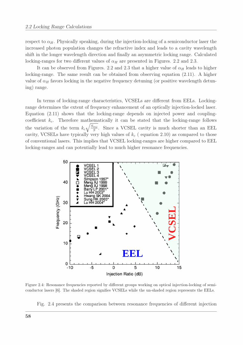
2.2 Locking Range Calculations
respect to αH . Physically speaking, during the injection-locking of a semiconductor laser the
increased photon population changes the refractive index and leads to a cavity wavelength
shift in the longer wavelength direction and finally an asymmetric locking range. Calculated
locking-ranges for two different values of αH are presented in Figures. 2.2 and 2.3.
It can be observed from Figures. 2.2 and 2.3 that a higher value of αH leads to higher
locking-range. The same result can be obtained from observing equation (2.11). A higher
value of αH favors locking in the negative frequency detuning (or positive wavelength detun-
ing) range.
In terms of locking-range characteristics, VCSELs are different from EELs. Locking-
range determines the extent of frequency enhancement of an optically injection-locked laser.
Equation (2.11) shows that the locking-range depends on injected power and coupling-
coefficient kc. Therefore mathematically it can be stated that the locking-range follows
the variation of the term kc
√Sinj
S. Since a VCSEL cavity is much shorter than an EEL
cavity, VCSELs have typically very high values of kc ( equation 2.10) as compared to those
of conventional lasers. This implies that VCSEL locking-ranges are higher compared to EEL
locking-ranges and can potentially lead to much higher resonance frequencies.
VC
SEL
EEL
Figure 2.4: Resonance frequencies reported by different groups working on optical injection-locking of semi-
conductor lasers [6]. The shaded region signifies VCSELs while the un-shaded region represents the EELs.
Fig. 2.4 presents the comparison between resonance frequencies of different injection
58

Chapter 2 : Simulation of Optically Injection-Locked VCSELs
locked systems. It is important to note that Simpson [7], Meng [8], Sung [9] and Barry
[10] have presented the results of optical injection-locking of EELs. Despite the fact that
EELs have larger emission windows as compared to VCSELs, which facilitate optical power
injection inside the follower laser cavity, resonance frequencies reported by Chrostowski et.
al for VCSELs 1, 2, 3 and 4 in Fig. 2.4 far exceed the resonance frequencies obtained using
EELs [6]. This is due to difference in value of kc for EELs and VCSELs. A typical kc value
for a VCSEL is of the order of 1013 while that of an EEL is of the order of 1010 which explains
the difference in locking-ranges and consequently resonance frequencies.
2.3 Small Signal Analysis
We begin by presenting once again the “Modified VCSEL Rate Equations”. The small signal
analysis is performed to derive the S21 response of an injection-locked VCSEL.
dN(t)
dt=
ηiI
qVact
− (A + BN(t) + CN(t)2)N(t) − vgGS(t) (2.20)
dS(t)
dt= ΓvgGS(t) − S(t)
τP
+vg
L
√S(t)Sinj cos(θ) + ΓBβN(t)2 (2.21)
dφ(t)
dt=
αHΓvga0
2(N(t) − Ntr) − ∆ω − vg
2L
√Sinj
S(t)sin(θ) (2.22)
Consider that a sinusoidal signal ∆Iejωt modulates a laser biased at current I. The
resulting expression for current I then becomes:
I(t) = I + ∆Iejωt (2.23)
Similarly, the carrier, photon and phase variations can be described as follows:
N(t) = N + ∆Nejωt (2.24)
S(t) = S + ∆Sejωt (2.25)
φ(t) = φ + ∆φejωt (2.26)
By putting
N =dN
dt(2.27)
S =dS
dt(2.28)
φ =dφ
dt(2.29)
59

2.3 Small Signal Analysis
we have
∆N(I,N, S) =∂N
∂I· ∆I +
∂N
∂N· ∆N +
∂N
∂S· ∆S (2.30)
∆S(N,S, φ) =∂S
∂N· ∆N +
∂S
∂S· ∆S +
∂N
∂φ· ∆φ (2.31)
∆φ(N,S, φ) =∂φ
∂N· ∆N +
∂φ
∂S· ∆S +
∂φ
∂φ· ∆φ (2.32)
The gain, as defined in equation (2.3), contains both the carrier and the photon terms.
Partial differentiation of the equation (2.3), with respect to the carrier and photon densities
N and S, yields two new variables GN and GS, where GN and GS are defined as:
GN =∂G
∂N=
a0
1 + ǫS(2.33)
GS = −∂G
∂S=
a0ǫ(N − Ntr)
(1 + ǫS)2(2.34)
Differentiating equation (2.5) , with respect to N , S and φ, therefore results in the
following set of three equations:
∂N
∂N· ∆N = (−(A + 2BN + 3CN2) − vgGNS)∆N (2.35)
∂N
∂S· ∆S = (−vgG + vgGSS)∆S (2.36)
∂N
∂I· ∆I =
ηi
qVact
∆I (2.37)
Similarly if we define a new variable ρ as:
ρ =vg
2L
√Sinj
S(2.38)
and differentiate equation (2.6) with respect to N , S and φ, we have the following set
of equations:
∂S
∂N· ∆N = (ΓvgGNS − 2βBN)∆N (2.39)
∂S
∂S· ∆S = (−ΓvgGSS + ρcos(θ))∆S (2.40)
∂S
∂φ· ∆φ = (−2 · ρSsin(θ))∆φ (2.41)
60
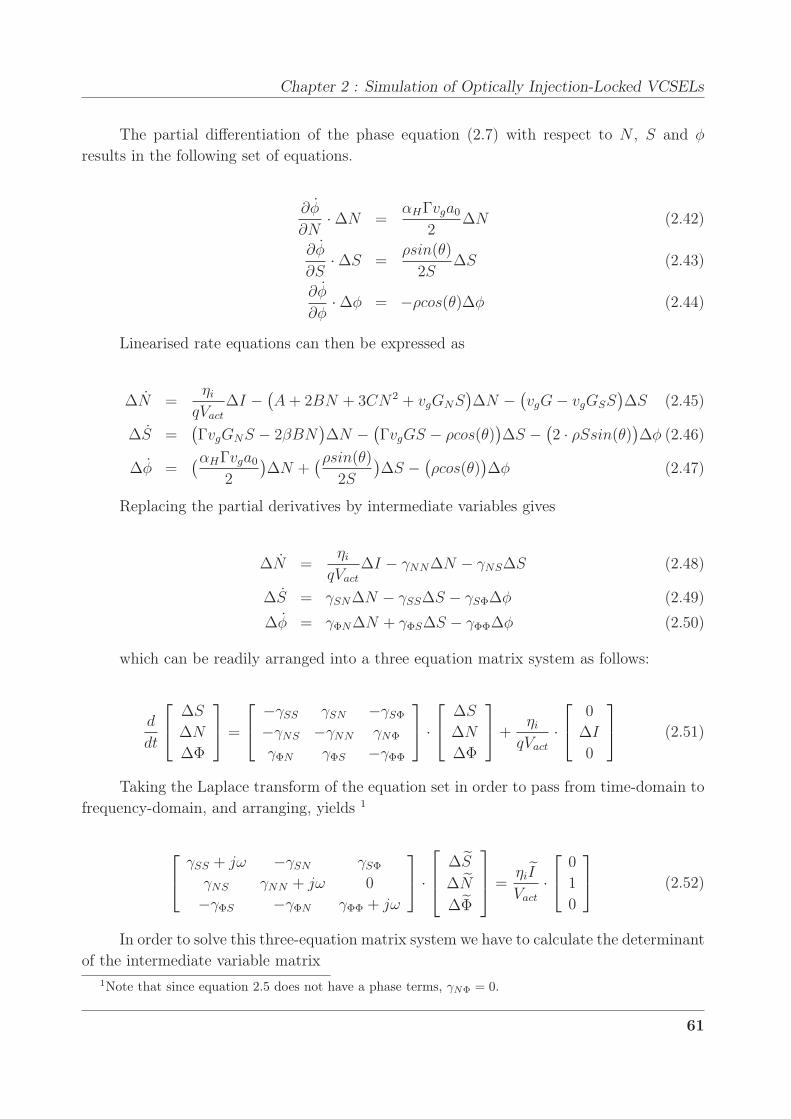
Chapter 2 : Simulation of Optically Injection-Locked VCSELs
The partial differentiation of the phase equation (2.7) with respect to N , S and φ
results in the following set of equations.
∂φ
∂N· ∆N =
αHΓvga0
2∆N (2.42)
∂φ
∂S· ∆S =
ρsin(θ)
2S∆S (2.43)
∂φ
∂φ· ∆φ = −ρcos(θ)∆φ (2.44)
Linearised rate equations can then be expressed as
∆N =ηi
qVact
∆I −(A + 2BN + 3CN2 + vgGNS
)∆N −
(vgG − vgGSS
)∆S (2.45)
∆S =(ΓvgGNS − 2βBN
)∆N −
(ΓvgGS − ρcos(θ)
)∆S −
(2 · ρSsin(θ)
)∆φ (2.46)
∆φ =(αHΓvga0
2
)∆N +
(ρsin(θ)
2S
)∆S −
(ρcos(θ)
)∆φ (2.47)
Replacing the partial derivatives by intermediate variables gives
∆N =ηi
qVact
∆I − γNN∆N − γNS∆S (2.48)
∆S = γSN∆N − γSS∆S − γSΦ∆φ (2.49)
∆φ = γΦN∆N + γΦS∆S − γΦΦ∆φ (2.50)
which can be readily arranged into a three equation matrix system as follows:
d
dt
∆S
∆N
∆Φ
=
−γSS γSN −γSΦ
−γNS −γNN γNΦ
γΦN γΦS −γΦΦ
·
∆S
∆N
∆Φ
+
ηi
qVact
·
0
∆I
0
(2.51)
Taking the Laplace transform of the equation set in order to pass from time-domain to
frequency-domain, and arranging, yields 1
γSS + jω −γSN γSΦ
γNS γNN + jω 0
−γΦS −γΦN γΦΦ + jω
·
∆S
∆N
∆Φ
=
ηiI
Vact
·
0
1
0
(2.52)
In order to solve this three-equation matrix system we have to calculate the determinant
of the intermediate variable matrix
1Note that since equation 2.5 does not have a phase terms, γNΦ = 0.
61

2.3 Small Signal Analysis
Λ =
∣∣∣∣∣
γSS + jω −γSN γSΦ
γNS γNN + jω 0
−γΦS −γΦN γΦΦ + jω
∣∣∣∣∣ (2.53)
where
Λ = −jω3
− ω2 (γNN + γSS + γΦΦ)
+ jω (γSΦγΦS + γSSγNN + γNSγSN + γNNγΦΦ + γSSγΦΦ)
+ (γSΦγΦSγNN − γSΦγNSγΦN + γSSγNNγΦΦ + γSNγNSγΦΦ) (2.54)
Using the Kramer’s rule, the photon density variation can be expressed as
∆S =ηiI
qVact
·
∣∣∣∣∣
0 −γSN γSΦ
1 γNN + jω 0
0 −γΦN γΦΦ + jω
∣∣∣∣∣
Λ(2.55)
Simplifying equation 2.55 leads to
∆S =ηiI
qVact
· (γSNγΦΦ − γΦNγNΦ) + jωγSN
Λ(2.56)
Equations 2.6 and 2.7 can alternatively be solved to obtain a relation in terms of the
phase difference between two lasers and is presented below:
θ = sin−1
∆ω
kc
√Sinj
S
√1 + α2
H
+ tan−1 αH
(2.57)
Using equation 2.57 we can incorporate the effects of frequency detuning into the small-
signal model of an injection-locked system since γΦΦ, γΦS, γSΦ and γSS depend on θ.
2.3.1 Theory and Physical Explanation
The increase in resonance frequency is a combination of two factors extraneous to the follower
laser and dependent on the injected light.
62

Chapter 2 : Simulation of Optically Injection-Locked VCSELs
• The injection of photons in the follower laser cavity changes the carrier-photon equi-
librium inside the cavity. The free-running follower laser cavity resonance that is
represented by the photon and carrier densities is redefined due to external light injec-
tion. The increase in photon density affects the carrier density inside the follower laser
cavity. The change in cavity resonance frequency due to carrier population density
variation can be quantified using αH ; the linewidth enhancement factor that indicates
the carrier-variation induced refractive index change and hence the amplitude-phase
coupling.
The consequence of the external photon-injection is hence a downshift in the laser
cavity resonance frequency denoted as ωDownshifted in this text.
• The second factor takes into account the difference between the master and the follower
lasing frequencies. This difference is known as “frequency detuning” and could be
defined as
∆ω = ωmaster − ωfollower (2.58)
The detuning is said to be positive if the master laser has an emission frequency greater
than that of the follower laser and is said to be negative if the reverse is true. Once locked
the follower laser emits at the same frequency as the master laser.
The follower laser, therefore, in effect is experiencing two different phenomena at the
same time. The external light injection has offset the cavity mode to a lower resonance
frequency while the detuning has led to a high emission frequency. It is the difference
between ωmaster and ωDownshifted that determines the value of enhanced resonance frequency,
ωEnhancedResonance of an optically injection-locked laser. The interference between ωmaster and
ωDownshifted generates a beat note whose value could be given as
ωEnhancedResonance = ωmaster − ωDownshifted (2.59)
The resonance peak observed in S21 curves of an optically injection-locked slave laser is
in fact the beat-note between the downshifted cavity resonance frequency, ωDownshifted, and
the master laser emission frequency ωmaster. This beat-note is amplified due to resonance
when the modulating frequency becomes equal to it. Fig. 2.5 represents the physical phe-
nomena taking place during the optical injection-locking procedure schematically.
Equation (2.59) explains the high resonance frequencies for optically injection-locked
follower lasers operating in positive frequency detuning regime. A positive frequency detun-
ing value leads to a high resonance frequency. These high resonance frequencies, however,
do not help in increasing the overall 3-dB bandwidth of the system because the resonance is
63
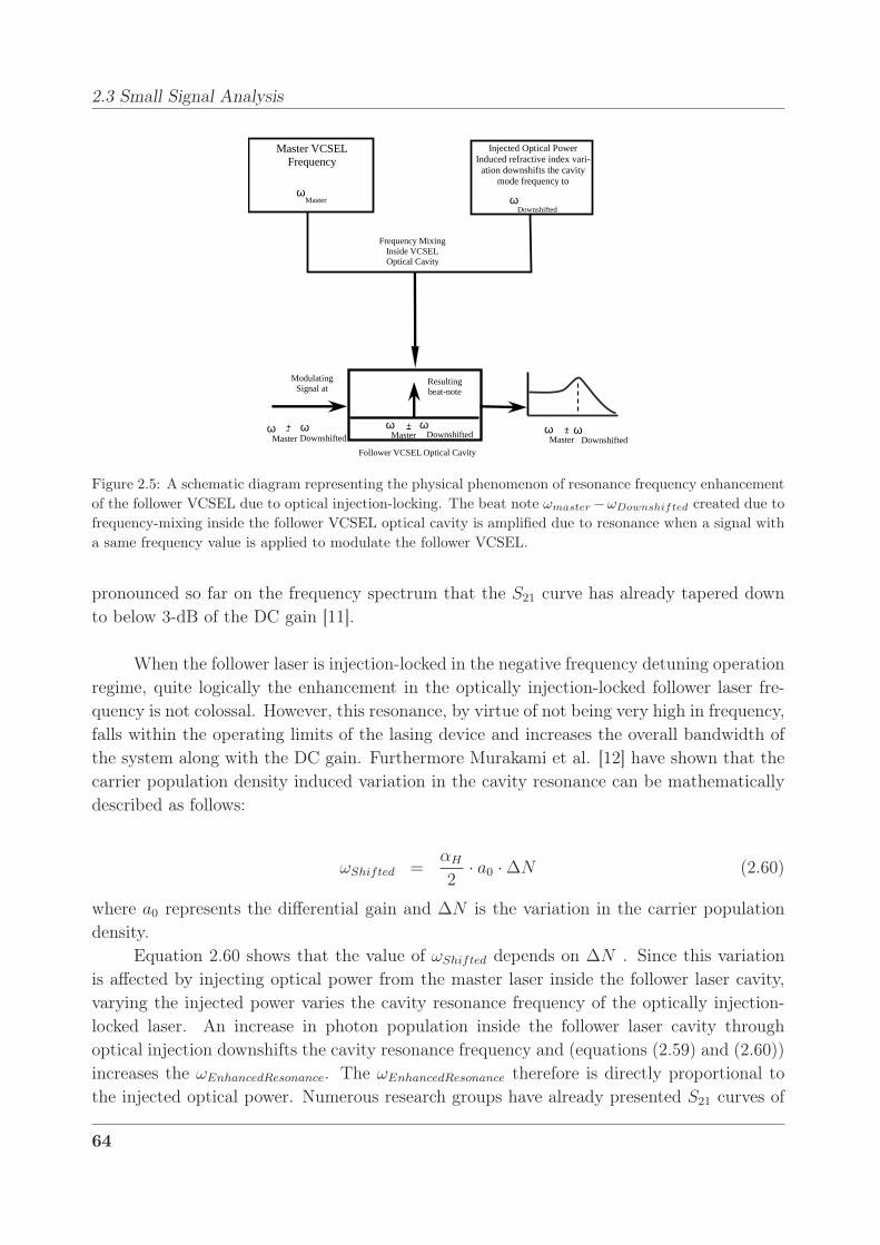
2.3 Small Signal Analysis
ωDownshifted
-
Injected Optical Power Induced refractive index vari-
ation downshifts the cavity mode frequency to
ωDownshifted
Master VCSEL Frequency
ωDownshifted-
Resulting beat-note
Modulating Signal at
ωDownshifted
-
Frequency Mixing Inside VCSEL Optical Cavity
Follower VCSEL Optical Cavity
ωMaster
ωMaster
ωMaster
ωMaster
++ +
Figure 2.5: A schematic diagram representing the physical phenomenon of resonance frequency enhancement
of the follower VCSEL due to optical injection-locking. The beat note ωmaster −ωDownshifted created due to
frequency-mixing inside the follower VCSEL optical cavity is amplified due to resonance when a signal with
a same frequency value is applied to modulate the follower VCSEL.
pronounced so far on the frequency spectrum that the S21 curve has already tapered down
to below 3-dB of the DC gain [11].
When the follower laser is injection-locked in the negative frequency detuning operation
regime, quite logically the enhancement in the optically injection-locked follower laser fre-
quency is not colossal. However, this resonance, by virtue of not being very high in frequency,
falls within the operating limits of the lasing device and increases the overall bandwidth of
the system along with the DC gain. Furthermore Murakami et al. [12] have shown that the
carrier population density induced variation in the cavity resonance can be mathematically
described as follows:
ωShifted =αH
2· a0 · ∆N (2.60)
where a0 represents the differential gain and ∆N is the variation in the carrier population
density.
Equation 2.60 shows that the value of ωShifted depends on ∆N . Since this variation
is affected by injecting optical power from the master laser inside the follower laser cavity,
varying the injected power varies the cavity resonance frequency of the optically injection-
locked laser. An increase in photon population inside the follower laser cavity through
optical injection downshifts the cavity resonance frequency and (equations (2.59) and (2.60))
increases the ωEnhancedResonance. The ωEnhancedResonance therefore is directly proportional to
the injected optical power. Numerous research groups have already presented S21 curves of
64

Chapter 2 : Simulation of Optically Injection-Locked VCSELs
optically injection-locked follower lasers to demonstrate this effect [6, 13, 14].
2.4 Numerical Simulations
2.4.1 VCSEL Intrinsic Parameters
Parameter Units Value
ηi - 0.8
τe ns 0.61
Nth cm−3 5.33x10¹⁸
Ntr cm−3 3.24x10¹⁸
A s−1 1.1x10⁸
B cm3/s 1x10⁻¹⁰
C cm6/s 3.57x10⁻²⁹
a0 cm2 4.8x10⁻¹⁶
vg cm/s 7.7x10⁹
ǫ cm3 2.2x10⁻¹⁷
τP ps 6.4
S cm−3 2.5x10¹⁵
Table 2.1: Long wavelength VCSEL intrinsic parameters used to simulate the small-signal injection-locking
behavior[15].
The mathematical model proposed above is implemented in MATLAB in order to
observe the small-signal response of an injection-locked system. Table. 2.1 summarizes the
VCSEL intrinsic parameters used to calculate the S21 response of an injection locked system
[15].
2.4.2 Simulation Results
Recently the most significant application of optical injection-locking has been in the domain
of resonance frequency enhancement. The enhanced resonance frequency can lead to an
extended bandwidth many times the original device bandwidth. The modulation response
of an injection-locked laser can be characterized as one of the following three:
• High Resonance Frequency, Low Bandwidth
• High Resonance Frequency, High Bandwidth
• Low Resonance Frequency, Low Bandwidth
65

2.4 Numerical Simulations
0 20 40 60 80−60
−50
−40−60
−40
−20
0
Frequency (GHz)
Nor
mal
ized
S21
Res
pons
e (d
B)
Inje
cted
Pow
er (d
Bm
)
Figure 2.6: Calculated S21 response of an optically injection-locked VCSEL with constant frequency detuning
and variable injection power from -60 dBm to -40 dBm.
Although, as presented in Fig. 2.6, the resonance frequency of an optically injection-
locked laser increases with increasing injected power levels, the frequency detuning between
the two lasers plays a very important role in determining the eventual characteristics of the
S21 curve and finally the effective bandwidth. The above presented three different kinds
of modulation responses depend on different locking conditions and parameters and are
described in the following section.
2.4.2.1 High Resonance Frequency, Low Bandwidth
The high resonance frequency, low bandwidth operation regime can be attributed to a posi-
tive frequency detuning. Since the resonance frequency of an injection-locked system is the
difference between the master laser frequency and the down shifted follower cavity frequency
( equation (2.59)), positive frequency detuning results in very high resonance frequencies. On
the other hand, optically injection-locked systems can be mathematically defined as third-
order systems and suffer from low-frequency dips due to the presence of a parasitic pole.
Figures. 2.7 and 2.8 present the simulated S21 response of an optically injection-locked
VCSEL operating in the positive frequency detuning regime. The injected optical power is
maintained constant for this set of curves in order to study the effects of variation in positive
frequency detuning. The resonance frequency increases with increasing difference between
the master and follower VCSEL frequencies.
Although from a telecommunication point of view, enhancement in resonance frequency
66
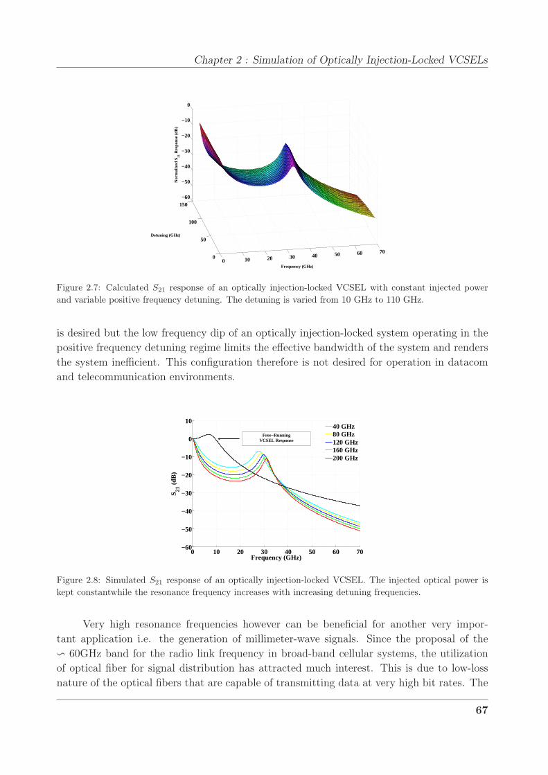
Chapter 2 : Simulation of Optically Injection-Locked VCSELs
0 10 20 30 40 50 60 700
50
100
150−60
−50
−40
−30
−20
−10
0
Frequency (GHz)
Detuning (GHz)
Nor
mal
ized
S21
Res
pons
e (d
B)
Figure 2.7: Calculated S21 response of an optically injection-locked VCSEL with constant injected power
and variable positive frequency detuning. The detuning is varied from 10 GHz to 110 GHz.
is desired but the low frequency dip of an optically injection-locked system operating in the
positive frequency detuning regime limits the effective bandwidth of the system and renders
the system inefficient. This configuration therefore is not desired for operation in datacom
and telecommunication environments.
0 10 20 30 40 50 60 70−60
−50
−40
−30
−20
−10
0
10
Frequency (GHz)
S 21 (
dB)
40 GHz80 GHz120 GHz160 GHz200 GHz
Free−RunningVCSEL Response
Figure 2.8: Simulated S21 response of an optically injection-locked VCSEL. The injected optical power is
kept constantwhile the resonance frequency increases with increasing detuning frequencies.
Very high resonance frequencies however can be beneficial for another very impor-
tant application i.e. the generation of millimeter-wave signals. Since the proposal of the
∽ 60GHz band for the radio link frequency in broad-band cellular systems, the utilization
of optical fiber for signal distribution has attracted much interest. This is due to low-loss
nature of the optical fibers that are capable of transmitting data at very high bit rates. The
67

2.4 Numerical Simulations
main obstacle in the implementation of this scheme is the conception of a high frequency
oscillator. Goldberg et. al had already demonstrated the generation of microwave signals
using injection-locked laser diodes in 1983 [16], but the enthusiasm in the implementation
of this scheme faded away due to the incipient nature of semiconductor lasers at that time.
Noel et al. presented an optical millimeter-wave generation technique in 1996 by locking
an FP laser in the positive detuning frequency operation regime [17]. In 1998 Braun et al.
demonstrated the generation of a low phase-noise millimeter-wave generation at 64GHz by
injection-locking the optical sideband of a laser [18]. Since then several research groups have
used optical injection-locking for millimeter-wave generation [9], [19], [20].
2.4.2.2 High Resonance Frequency, High Bandwidth
Positive frequency detuning can be employed to achieve very high resonance frequencies
that could be useful for certain applications such as microwave and millimeter-wave signal
generation but such high resonance frequencies imply very low cut-off frequencies due to
low-frequency dip associated to positive frequency detuning. This situation can be improved
by operating the laser at close to zero detuning.
0 5 10 15 20 25 30 35 40−25
−20
−15
−10
−5
0
−3
Frequency (GHz)
S 21 (
dB)
Figure 2.9: Simulated S21 response of an optically injection-locked follower VCSEL showing cut-off frequency
enhancement.
In such a configuration, the cut-off frequency increases with increase in injected power
but due to very low frequency detuning value there is no loss at low frequency values.
Frequency detuning has little or no effect on the resonance frequency of such a system and
the bandwidth increase is dependent only on optical injected power. This configuration can
be employed for broadband digital communications that require the transmission of very
high bit rates.
68

Chapter 2 : Simulation of Optically Injection-Locked VCSELs
2.4.2.3 Low Resonance Frequency, Low Bandwidth
The third operation regime is defined by negative frequency detuning. Fig. 2.10 presents
a set of simulated S21 curves with increasing negative frequency detuning. It is clear from
Fig. 2.10 that for positive frequency detuning values, the follower VCSEL S21 response is
undamped with high resonance frequencies. However when the detuning between the two
VCSELs is varied in the negative detuning operation regime, the S21 response curves start to
become highly damped. At the same time, the low frequency dip, exhibited due to positive
frequency detuning operation regime starts to disappear. Finally at relatively high values
of negative frequency detuning the S21 curves become over-damped and gradually the reso-
nance peak vanishes.
0 10 20 30 40 50 60 70
−100
−90
−80
−70
−60
−50−50
−40
−30
−20
−10
0
Frequency (GHz)
Detuning (GHz)
Nor
mal
ized
S21
Res
pons
e (d
B)
Figure 2.10: Calculated S21 response of an optically injection-locked VCSEL with constant injected power
and variable negative detuning. The detuning is varied from 10 GHz to -190 GHz.
The negative frequency detuning can hence be used to generate high low frequency
gain S21 curves. This is particularly important for directly modulated optical fiber links.
The losses in such links, apart from coupling and connector losses, are due to Electrical-
Optical (E/O) and Optical-Electrical (O/E) conversion. Sung et al. have demonstrated that
by injection-locking a laser in negative frequency detuning regime the RF link gain can be
improved by up to 10 dB [21].
69

2.5 Comparison between Free-Running and Injection-Locked VCSEL Models
100
101−50
−40
−30
−20
−10
0
10
Frequency (GHz)
S 21 (
dB)
Slope:−18dB/Octave
Slope:−12dB/Octave
Figure 2.11: Comparison between the free-running and injection-locked transfer functions of a VCSEL.
2.5 Comparison between Free-Running and Injection-Locked
VCSEL Models
Fig. 2.11 presents a comparison between the free-running and injection-locked S21 response of
a VCSEL. The frequency responses are plotted on a logarithmic scale in order to highlight the
difference between the respective slopes of the two systems. The injection-locked system has
a slope of -18dB/octave as compared to a slope of -12dB/octave for a free-running VCSEL.
Another important difference of note is the low frequency dip in the optically injection-locked
VCSEL S21 response which is due to the extra pole in the transfer function denominator (ref.
equation 2.56).
By putting Sinj and ∆ω equal to zero the modified VCSEL rate equations (equations
2.5, 2.6, 2.7) are reduced to classical VCSEL rate equations (equations 2.1, 2.2, 2.4). Fig-
ure.2.12 presents a comparison between the S21 responses of a free-running and an injection-
locked VCSEL using the same set of modified rate equations.
0 5 10 15 20 25 30 35 40
−25
−20
−15
−10
−5
0
−3
Frequency (GHz)
S 21 (
dB)
Free−RunningVCSEL
S21
Response
Injection−LockedVCSEL
S21
Response
Figure 2.12: Free-Running VCSEL S21 response calculated by putting Sinj and ∆ω equal to zero in equations
2.5, 2.6 and 2.7.
70
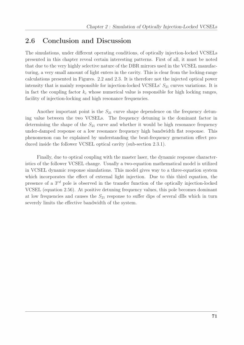
Chapter 2 : Simulation of Optically Injection-Locked VCSELs
2.6 Conclusion and Discussion
The simulations, under different operating conditions, of optically injection-locked VCSELs
presented in this chapter reveal certain interesting patterns. First of all, it must be noted
that due to the very highly selective nature of the DBR mirrors used in the VCSEL manufac-
turing, a very small amount of light enters in the cavity. This is clear from the locking-range
calculations presented in Figures. 2.2 and 2.3. It is therefore not the injected optical power
intensity that is mainly responsible for injection-locked VCSELs’ S21 curves variations. It is
in fact the coupling factor kc whose numerical value is responsible for high locking ranges,
facility of injection-locking and high resonance frequencies.
Another important point is the S21 curve shape dependence on the frequency detun-
ing value between the two VCSELs. The frequency detuning is the dominant factor in
determining the shape of the S21 curve and whether it would be high resonance frequency
under-damped response or a low resonance frequency high bandwidth flat response. This
phenomenon can be explained by understanding the beat-frequency generation effect pro-
duced inside the follower VCSEL optical cavity (sub-section 2.3.1).
Finally, due to optical coupling with the master laser, the dynamic response character-
istics of the follower VCSEL change. Usually a two-equation mathematical model is utilized
in VCSEL dynamic response simulations. This model gives way to a three-equation system
which incorporates the effect of external light injection. Due to this third equation, the
presence of a 3rd pole is observed in the transfer function of the optically injection-locked
VCSEL (equation 2.56). At positive detuning frequency values, this pole becomes dominant
at low frequencies and causes the S21 response to suffer dips of several dBs which in turn
severely limits the effective bandwidth of the system.
71

BIBLIOGRAPHY
Bibliography
[1] R. Lang, “Injection Locking Properties of a Semiconductor Laser,” IEEE Journal of
Quantum Electronics, vol. 18, no. 6, pp. 976–983, Jun 1982.
[2] P. Gallion and G. Debarge, “Influence of amplitude-phase coupling on the injection
locking bandwidth of a semiconductor laser,” Electronics Letters, vol. 21, no. 7, pp.
264–266, 28 1985.
[3] P. Gallion, H. Nakajima, G. Debarge, and C. Chabran, “Contribution of spontaneous
emission to the linewidth of an injection-locked semiconductor laser,” Electronics Let-
ters, vol. 21, no. 14, pp. 626–628, 4 1985.
[4] C. Henry, N. Olsson, and N. Dutta, “Locking Range and Stability of Injection Locked
1.54µm InGaAsp Semiconductor Lasers,” IEEE Journal of Quantum Electronics, vol. 21,
no. 8, pp. 1152–1156, Aug 1985.
[5] I. Petitbon, P. Gallion, G. Debarge, and C. Chabran, “Locking bandwidth and relax-
ation oscillations of an injection-locked semiconductor laser,” IEEE Journal of Quantum
Electronics, vol. 24, no. 2, pp. 148–154, Feb 1988.
[6] L. Chrostowski, X. Zhao, and C. Chang-Hasnain, “Microwave Performance of Optically
Injection-locked VCSELs,” IEEE Transactions on Microwave Theory and Techniques,
vol. 54, no. 2, pp. 788–796, Feb. 2006.
[7] T. Simpson, J. Liu, and A. Gavrielides, “Small-signal analysis of modulation charac-
teristics in a semiconductor laser subject to strong optical injection,” IEEE Journal of
Quantum Electronics, vol. 32, no. 8, pp. 1456–1468, Aug 1996.
[8] X. Meng, T. Chau, D. Tong, and M. Wu, “Suppression of Second Harmonic Distor-
tion in Directly Modulated Distributed Feedback Lasers by External Light Injection,”
Electronics Letters, vol. 34, no. 21, pp. 2040–2041, Oct 1998.
[9] H. Kee-Sung, T. Jung, M. Wu, D. Tishinin, K. Liou, and W. Tsang, “Optical generation
of millimeter-waves using monolithic sideband injection locking of a two-section DFB
laser,” The 16th Annual Meeting of the IEEE Lasers and Electro-Optics Society. LEOS
2003., vol. 2, pp. 1005–1006 vol.2, Oct. 2003.
[10] L. Barry, P. Anandarajah, and A. Kaszubowska, “Optical pulse generation at frequencies
up to 20 GHz using external-injection seeding of a gain-switched commercial Fabry-Perot
laser,” IEEE Photonics Technology Letters, vol. 13, no. 9, pp. 1014–1016, Sep 2001.
[11] L. Chrostowski, F. B., W. Hoffman, M.-C. Amann, S. Wieczorek, and W. Chow, “40 GHz
Bandwidth and 64 GHz Resonance Frequency in Injection-Locked 1.55 µm VCSELs,”
IEEE Journal of Journal of Selected Topics in Quantum Electronics, vol. Vol. 13, No.
5, 2007.
72

Chapter 2 : Simulation of Optically Injection-Locked VCSELs
[12] A. Murakami, K. Kawashima, and K. Atsuki, “Cavity Resonance Shift and Bandwidth
Enhancement in Semiconductor Lasers With Strong Light Injection,” IEEE Journal of
Quantum Electronics, vol. 39, no. 10, pp. 1196–1204, Oct. 2003.
[13] X. Zhao, E. K. Lau, D. Parekh, H.-K. Sung, W. Hofmann, M. C. Amann, M. C. Wu,
and C. J. Chang-Hasnain, “107-GHz Resonance Frequency of 1.55µm VCSELs Under
Ultra-high Optical Injection Locking,” in OSA/CLEO, 2008.
[14] X. Zhao, M. Moewe, L. Chrostowski, C.-H. Chang, R. Shau, M. Ortsiefer, M.-C. Amann,
and C. Chang-Hasnain, “28 GHz Optical Injection-Locked 1.55µm VCSELs,” IEE Elec-
tronic Letters, vol. Vol. 40 No. 8, 15 April 2004.
[15] A. Bacou, “Caractérisation et Modélisation optoélectronique de VCSEL à grande
longueur d’onde pour sous-ensembles optiques intégrés,” Ph.D. dissertation, Institut
Supérieur de l’Aéronautique et de l’Espace, 2008.
[16] L. Goldberg, H. Taylor, J. Weller, and D. Bloom, “Microwave signal generation with
injection-locked laser diodes,” Electronics Letters, vol. 19, no. 13, pp. 491–493, 23 1983.
[17] L. Noel, D. Marcenac, and D. Wake, “Optical millimetre-wave generation technique with
high efficiency, purity and stability,” Electronics Letters, vol. 32, no. 21, pp. 1997–1998,
Oct 1996.
[18] R.-P. Braun, G. Grosskopf, D. Rohde, and F. Schmidt, “Low-phase-noise millimeter-
wave generation at 64 GHz and data transmission using optical sideband injection lock-
ing,” Photonics Technology Letters, IEEE, vol. 10, no. 5, pp. 728–730, May 1998.
[19] Z. Ahmed, H. Liu, D. Novak, Y. Ogawa, M. Pelusi, and D. Kim, “Locking characteristics
of a passively mode-locked monolithic DBR laser stabilized by optical injection,” IEEE
Photonics Technology Letters, vol. 8, no. 1, pp. 37–39, Jan. 1996.
[20] J. Hong and R. Hui, “Tunable millimeter-wave generation with subharmonic injection
locking in two-section strongly gain-coupled DFB lasers,” IEEE Photonics Technology
Letters, vol. 12, no. 5, pp. 543–545, May 2000.
[21] H.-K. Sung, T. Jung, D. Tishinin, K. Liou, W. Tsang, and M. Wu, “Optical Injection-
Locked Gain-Lever Distributed Bragg Reflector Lasers With Enhanced RF Perfor-
mance,” IEEE International Topical Meeting on Microwave Photonics. MWP’2004.,
pp. 225–228, Oct. 2004.
73


Chap
ter
3 Optical Injection-Locking Ex-
periments
The injection-locking experiments carried-out during the course of this work evolved progres-
sively in their complexity. The objective was to demonstrate and understand the VCSEL-
by-VCSEL optical injection-locking phenomena under different operating constraints. Our
focus was the study of variations in S21 response of injection-locked VCSELs under different
injection powers and varying detuning frequencies.
3.1 Experiments using Multimode Lasers
3.1.1 Multimode Edge Emitting Lasers (EELs)
Optically injection-locked lasers are known to overcome many fundamental limitations of
free-running systems. One of the very important improvements proposed by the employ-
ment of the optical injection-locking technique is the side-mode suppression of a multimode
laser [1]. figure 3.1 presents the super-imposed optical spectra of a free-running and an
injection-locked laser diode. The Fabry-Pérot modes, visible in the free-running regime, un-
dergo approximately 35 dB suppression when injection-locked using a DFB laser diode.
1311.57nm 1316.57nm 1321.57nm2.0nm/div
Peak 1316.11nm
0.2dBm
-49.8dBm
-99.8dBm
Wavlength (nm)
Free-Running Injection-Locked
Figure 3.1: The super-imposed spectra of a free running and an injection locked Fabry-Pérot EEL. Mode
suppression can be observed in the injection locked spectrum.
In the stable locking regime (figure 3.2) the follower laser frequency is locked to the
master laser lasing frequency. The injection-locked Fabry-Pérot mode therefore becomes
dominant and the unlocked modes are suppressed. Iwashita et. al demonstrated the uti-
lization of this method for the suppression of mode-partition noise [1]. The employment of
optical-injection locking for side-mode suppression in VCSELs however is not very effective.
75

3.1 Experiments using Multimode Lasers
This is due to the difference in the side-mode generation mechanism between the EELs and
the VCSELs. A detailed analysis of side-mode generation is presented in the following section.
−43 −42 −41 −40 −39 −38 −37 −36 −35 −34 −33−140
−120
−100
−80
−60
−40
−20
0
20
40
Injected Power (dBm)
Det
unin
g F
requ
ency
(G
Hz)
Unstable OperationRegion
Unstable OperationRegion
Figure 3.2: 2D presentation of calculated locking range of a long wavelength VCSEL with αH = 3 showing
the locking-range dependence on injected optical power.
Single-mode operation of the follower laser however is highly desirable due to another
very important reason. As presented in figure 3.2, the locking-range of an injection-locked
laser, in the “stable operation region”, is dependent on the injected optical power. This
effective locking-range is exploitable only if the follower laser is single-mode. If the follower
laser is multimode, the achievable detuning frequency is limited by the Free Spectral Range
(FSR) of the follower laser. At large detuning frequencies, the master laser might come closer
to an adjacent longitudinal mode and in that case, it will lock the adjacent longitudinal mode
instead of sweeping the entire locking range with previously locked mode. This mode-hopping
reduces the effective “locking” and hence “operation range” of an injection-locked system.
3.1.2 Multimode VCSELs
Figure 3.3 presents the optical spectrum of a multimode VCSEL. The VCSEL in question is
manufactured by Vertials with a threshold current of 6 mA and peak output optical power
of 20 mW. The VCSEL chip was powered-up using a probe-station. The master laser is
single-mode Vertilas VCSEL emitting in the 1.55µm range. A comparison with figure 3.4
shows that optical injection-locking fails to produce an effect similar to that demonstrated
previously on multimode EELs. Although a nominal side-mode suppression is observed in
the injection-locked follower VCSEL spectrum, the emission spectrum rests multimode.
76

Chapter 3 : Optical Injection-Locking Experiments
1560.00 1556.081548.08 0.8nm/Div
Wavelength (nm)
-126.4dBm
-76.4dBm
-26.4dBm
Figure 3.3: Optical spectrum of an Vertilas multimode “Power” VCSEL. The VCSEL threshold current is
about 6 mA.
1553.08 1555.581550.58 0.55nm/Div
Wavelength (nm)
-122.6dBm
-72.6dBm
-22.6dBm
Injection-Locked Mode
Figure 3.4: Spectrum of an optically injection-locked multimode Vertilas VCSEL. The threshold current is
about 6 mA. A very feeble side-mode suppression is observed due to injection-locking.
77
3.2 Experiments using Single-Mode VCSELs
This can be explained by developing an understanding of the side-mode generation
phenomena in VCSELs. The active region of a VCSEL is very short as compared to that of
an EEL, essentially of the order of the emission wavelength. Consequently, only one Fabry-
Pérot mode exists in the VCSELs, since the physical dimensions of the cavity eliminate the
possibility of longitudinal multi-mode lasing action. Therefore VCSELs are fundamentally
single-mode emission devices. However, the confinement and guiding of the optical field
thus generated is made very difficult due to a very peculiar VCSEL structural characteristic.
VCSEL design suggests the sharing of a common path for photons and carriers, moving
through the DBRs. This leads to the heating of the DBRs due to carrier flow and results
in a variable refractive index distribution inside the VCSEL optical cavity. The creation of
non-uniform refractive index zones inside the optical cavity leads to different optical paths
and has an overall dispersive effect. This phenomenon is known as “Thermal Lensing”.
The electrons passing through the DBRs tend to concentrate on the edge of the active
zone due to the oxide aperture-based carrier guiding. A higher carrier concentration at the
fringes of the active zone translates into higher photon generation at the edges of the active
zone. Instead of being concentrated in the center of the optical cavity, in the form of a sin-
gle transverse mode, the optical energy is repartitioned azimuthally inside the optical cavity.
The creation of non-uniform refractive index zones within the VCSEL optical cavity, changes
the effective optical path inside the cavity which manifests itself in the form of undesired
side-modes. Since the VCSEL side-modes are a consequence of spatial energy distribution,
they are referred to as “Spatial” or “Transverse Modes”.
Higher bias currents therefore imply high optical power and in consequence a higher
number of transverse modes. An oxide-aperture is employed in order to achieve optimal
current confinement and to block unwanted transverse modes. The oxide-aperture diameter
determines the multimode or single mode character of a VCSEL. VCSELs having oxide aper-
ture diameters greater than 5µm exhibit a multimode behavior. It can also be inferred from
the above discussion that for the type of VCSELs employing the oxide-aperture technology
for optical confinement, single mode VCSELs almost always have emission powers less than
those of multimode VCSELs. Since the Vertilas VCSEL used here is a high power device,
it has a Buried Tunnel Junction (BTJ) diameter of 20µm and is therefore distinctly multi-
mode. Since optical injection-locking favors single-mode operation by eliminating longitudi-
nal modes and since the modes generated in VCSELs are not longitudinal, the employment
of optical injection-locking for single-mode VCSEL operation is not very effective.
78

Chapter 3 : Optical Injection-Locking Experiments
1 2 3 4 5 6 7 8 9 100
0.2
0.4
0.6
0.8
1
1.2
1.4
Current (mA)
Opt
ical
Pow
er (
mW
)
(a) L-I curve
1556.54nm 1560.654 1564.6540.80nm
-14.7 dBm
-74.7 dBm
-44.7 dBm
Wavelength (nm)
40 dB
(b) Optical spectrum
Figure 3.5: L-I curve (a) and Optical spectrum (b) of a Vertilas VCSEL with an emission wavelength of
1.55µm.
3.2 Experiments using Single-Mode VCSELs
3.2.1 Experiments Using Vertilas VCSELs
A logical step, after trying optical injection-locking of multimode VCSELs, was to attempt
the injection-locking of single-mode VCSELs. The VCSELs used for initial injection-locking
experiments were manufactured by Vertilas GmbH. These are single-mode, TO-46 packaged,
pigtailed, Buried Tunnel Junction (BTJ) devices with an emission wavelength of 1.55µm.
The L-I curve of the follower VCSEL is presented in figure 3.5 (a). The mode suppression
ratio between the fundamental and the side-mode is approximately 40 dBs.
Figures. 3.6 and 3.7 present the measurement test bench and the master and follower
laser spectra respectively.
The injection-locking experiments using Vertilas VCSELs were simple to carry-out due
to the pigtailed nature of the components, that made the optical power-injection inside the
follower VCSEL cavity relatively easy. The well known phenomenon of side-mode suppres-
sion (as demonstrated with EELs and presented in figure 3.4) was observed. When the
VCSEL satellite mode is optically injection-locked, the fundamental mode undergoes a rapid
diminution and the VCSEL output optical power shifts to the side-mode wavelength. How-
ever, other than being a proof of concept demonstration, this exercise proved to be of little
significance. The real price of this ease of manipulation was paid in terms of a degraded
frequency response. The TO-46 package cut-off frequency was about 5 Ghz which was
well below the component cut-off frequency (11 GHz). The observation of injection-locked
VCSELs’ S21 response under various injection conditions was therefore not possible.
79
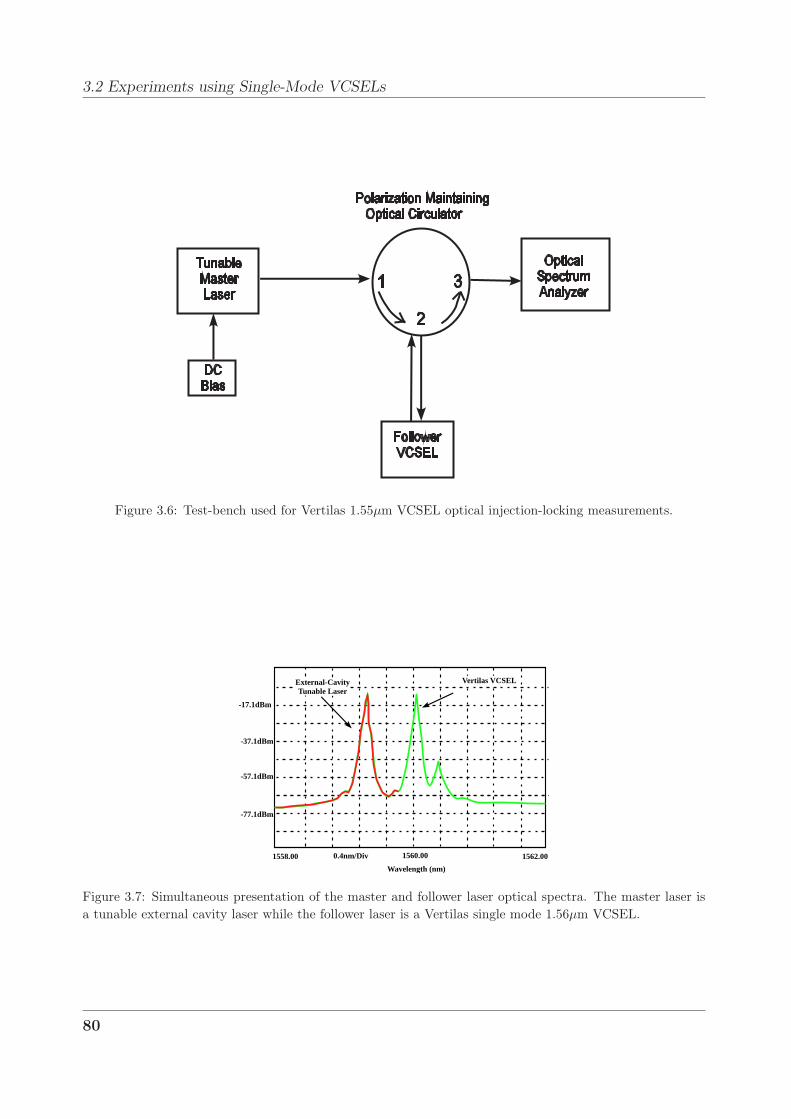
3.2 Experiments using Single-Mode VCSELs
Figure 3.6: Test-bench used for Vertilas 1.55µm VCSEL optical injection-locking measurements.
1560.00 1562.001558.00 0.4nm/Div
-77.1dBm
-57.1dBm
-37.1dBm
-17.1dBm
Wavelength (nm)
External-Cavity Tunable Laser
Vertilas VCSEL
Figure 3.7: Simultaneous presentation of the master and follower laser optical spectra. The master laser is
a tunable external cavity laser while the follower laser is a Vertilas single mode 1.56µm VCSEL.
80

Chapter 3 : Optical Injection-Locking Experiments
1560.00 1562.001558.00 0.4nm/Div
-77.1dBm
-57.1dBm
-37.1dBm
-17.1dBm
Wavelength (nm)
Optically Injection-Locekd VCSEL fundamental Mode
Suppressed Sidemode
(a)
1560.00 1562.001558.00 0.4nm/Div
-77.1dBm
-57.1dBm
-37.1dBm
-17.1dBm
Wavelength (nm)
Optically Injection-Locekd VCSEL Side Mode
Suppressed Fundamental Mode
(b)
Figure 3.8: (a) Optical spectrum of an optically injection-locked Vertilas VCSEL. The locking of fundamental
mode further suppresses the side-mode. (b) Optical spectrum of an optically injection-locked Vertilas VCSEL.
The locking of side mode has suppressed the fundamental lasing mode. Notice the position of the suppressed
modes in the two different cases.
3.2.2 Experiments Using BeamExpress VCSELs
In 2007, in the context of a trans-national project 1, VCSEL injection-locking studies were
undertaken using BeamExpress VCSELs. Markedly different technologically and function-
ally from Vertilas VCSELs, BeamExpress VCSELs opened-up very interesting and unique
research possibilities. Their on-chip availability, along with a comprehensive information
about their structure and their fabrication technique, presented following unparalleled ad-
vantages:
• The on-chip configuration eliminated the problems associated to parasitics introduced
by packaging. This also suggested the possibility of observation of device intrinsic S21
response.
• The fabrication process and device structure knowledge allowed the extraction of in-
trinsic parameters, that in turn led to reliable injection-locking simulations 2.
• Disposal of VCSELs from the same wafer allowed to observe the identical VCSEL-by-
VCSEL optical injection-locking for various applications.
Although the on-chip VCSEL-by-VCSEL optical injection-locking, as discussed above,
presented many interesting possibilities, its physical implementation proved to be quite chal-
lenging. The biggest problem encountered was optical power coupling from the VCSEL
1The MNT Eranet Project focusing on the development of VCSEL modules for Coarse Wavelength Divi-
sion Multiplexing (CWDM) and for optical networks.2For a comprehensive discussion on VCSEL optical cavity intrinsic response, parasitics associated with
on-chip VCSEL performance and VCSEL-chip intrinsic parameter extraction refer to [2].
81

3.2 Experiments using Single-Mode VCSELs
emission window into the optical fiber for utilization in the fairly classical set-up proposed
in figure 3.9.
Figure 3.9: Optical injection-locking setup using a polarization maintaining optical circulator. A semicon-
ductor optical amplifier (SOA) connected to port 1 is used to vary the injected optical power.
The VCSELs S21 response was observed using an HP-8510C Vector Network Analyzer
(VNA) operating up to 20 GHz. An optical rack is integrated to the VNA which consists
of a calibrated photodiode for Optical-Electrical conversion. The VCSEL optical output
was directly provided to this calibrated photodiode. A schematic representation of the
experimental set-up used to measure the S21 response of an on-chip VCSEL using a VNA is
given in figure 3.10.
Calibrated Photodiode
VCSEL ChipRF
Probe
Lensed Fiber
VNA
Port1 Port2
Optical Rack
Numeric Pad
Figure 3.10: Schematic representation of the experimental setup used to measure the S21 response of an
on-chip VCSEL using a vector network analyzer.
82

Chapter 3 : Optical Injection-Locking Experiments
The L-I curves for the set of VCSELs used in this experiment are presented in figures
3.11 and 3.12. Since no temperature control was applied to the VCSELs during the course of
this work, the VCSEL wavelength variation (δλ) was achieved by changing the bias current.
Representative λ-I tuning curves are also given in figures 3.11 and 3.12. In order to vary
the injected optical power, without altering the master VCSEL emission wavelength and
hence the detuning frequency value, an Optical Semiconductor Amplifier (OSA) has been
utilized. The maximum optical output power collected using a lensed multimode fiber is
approximately 2 mW. Although 2 mW appears to be sufficient to carry-out injection-locking
experiments, it must be noted that in this instance, the optical power is collected using a
multimode fiber. The utilization of the polarization maintaining optical circulator requires
the employment of a single-mode fiber which restricts the maximum available optical power
to about 0.4 mW.
2 3 4 5 6 7 8 9 100
0.5
1
1.5
2
2.5
Current (mA)
Opt
ical
Pow
er (
mA
)
(a) Optical Power vs. Bias Current
2 3 4 5 6 7 8 9 101321
1322
1323
1324
1325
1326
1327
Current (mA)
Wav
elen
gth
(nm
)
(b) Wavelength Tuning
Figure 3.11: The L-I curves for the first set of BeamExpress VCSELs used in this experiment. Representative
wavelength-bias current tuning curves are also given.
2 3 4 5 6 7 8 9 100
0.5
1
1.5
2
Current (mA)
Opt
ical
Pow
er (
mW
)
(a) Optical Power vs. Bias Current
2 3 4 5 6 7 8 9 101317
1318
1319
1320
1321
1322
1323
1324
Current (mA)
Wav
elen
gth
(nm
)
(b) Wavelength Tuning
Figure 3.12: The L-I curves for the second set of BeamExpress VCSELs used in this experiment. Represen-
tative wavelength-bias current tuning curves are also given.
83
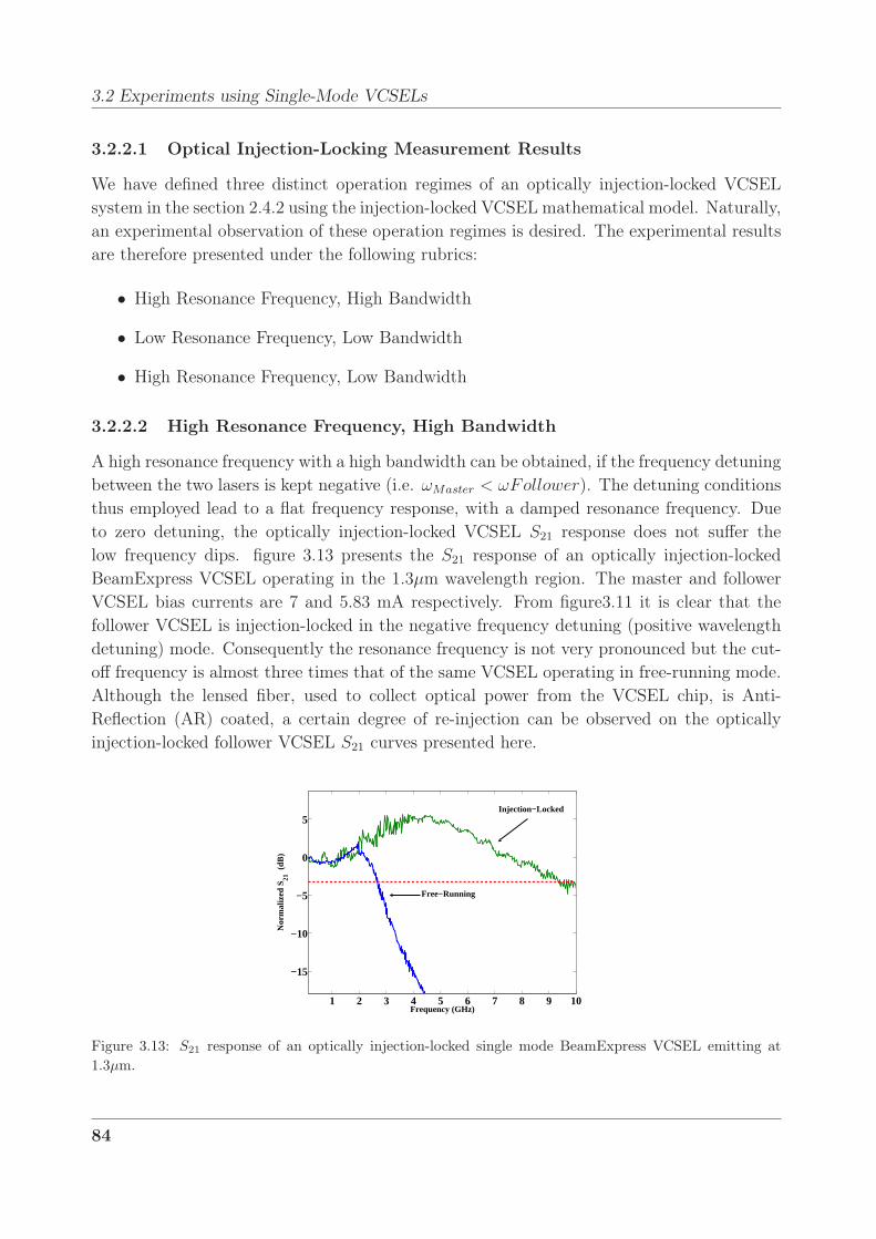
3.2 Experiments using Single-Mode VCSELs
3.2.2.1 Optical Injection-Locking Measurement Results
We have defined three distinct operation regimes of an optically injection-locked VCSEL
system in the section 2.4.2 using the injection-locked VCSEL mathematical model. Naturally,
an experimental observation of these operation regimes is desired. The experimental results
are therefore presented under the following rubrics:
• High Resonance Frequency, High Bandwidth
• Low Resonance Frequency, Low Bandwidth
• High Resonance Frequency, Low Bandwidth
3.2.2.2 High Resonance Frequency, High Bandwidth
A high resonance frequency with a high bandwidth can be obtained, if the frequency detuning
between the two lasers is kept negative (i.e. ωMaster < ωFollower). The detuning conditions
thus employed lead to a flat frequency response, with a damped resonance frequency. Due
to zero detuning, the optically injection-locked VCSEL S21 response does not suffer the
low frequency dips. figure 3.13 presents the S21 response of an optically injection-locked
BeamExpress VCSEL operating in the 1.3µm wavelength region. The master and follower
VCSEL bias currents are 7 and 5.83 mA respectively. From figure3.11 it is clear that the
follower VCSEL is injection-locked in the negative frequency detuning (positive wavelength
detuning) mode. Consequently the resonance frequency is not very pronounced but the cut-
off frequency is almost three times that of the same VCSEL operating in free-running mode.
Although the lensed fiber, used to collect optical power from the VCSEL chip, is Anti-
Reflection (AR) coated, a certain degree of re-injection can be observed on the optically
injection-locked follower VCSEL S21 curves presented here.
1 2 3 4 5 6 7 8 9 10
−15
−10
−5
0
5
Frequency (GHz)
Nor
mal
ized
S21
(dB
)
Injection−Locked
Free−Running
Figure 3.13: S21 response of an optically injection-locked single mode BeamExpress VCSEL emitting at
1.3µm.
84

Chapter 3 : Optical Injection-Locking Experiments
0 2 4 6 8 10
−15
−10
−5
0
5
Frequency (GHz)
Nor
mal
ized
S21
(dB
)
Free−Running Injection−Locked
Increasing injectedoptical power
Figure 3.14: S21 response of an optically injection-locked single mode BeamExpress VCSEL emitting at
1.3µm. Several S21 curves are obtained with increasing injected optical power for a constant negative
frequency detuning. P1>P2>P3>P4
2 3 4 5 6 73
4
5
6
7
8
9
10
11
Incident Optical Power (dBm)
Cut
−of
f Fre
quen
cy (
GH
z)
Figure 3.15: Cut-Off frequency variation of injection-locked BeamExpress VCSELs with increase in optical
injected power. All the measurements were made in the negative detuning frequency operation regime.
85
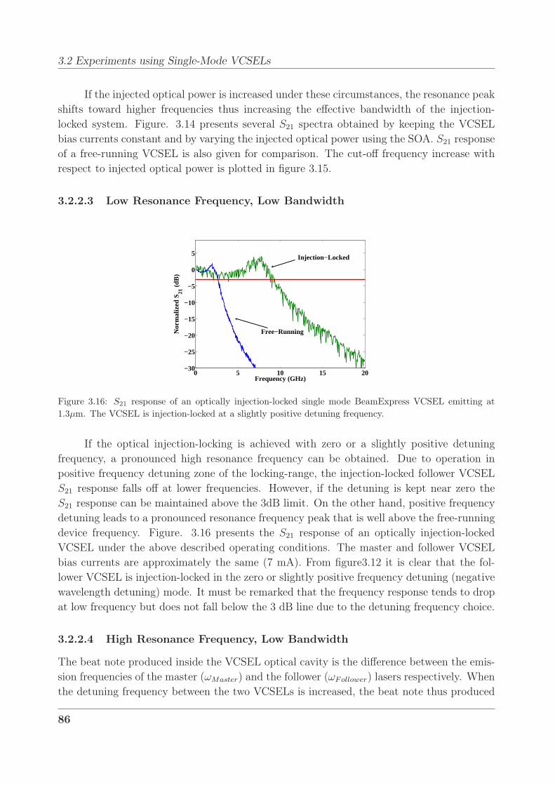
3.2 Experiments using Single-Mode VCSELs
If the injected optical power is increased under these circumstances, the resonance peak
shifts toward higher frequencies thus increasing the effective bandwidth of the injection-
locked system. Figure. 3.14 presents several S21 spectra obtained by keeping the VCSEL
bias currents constant and by varying the injected optical power using the SOA. S21 response
of a free-running VCSEL is also given for comparison. The cut-off frequency increase with
respect to injected optical power is plotted in figure 3.15.
3.2.2.3 Low Resonance Frequency, Low Bandwidth
0 5 10 15 20−30
−25
−20
−15
−10
−5
0
5
Frequency (GHz)
Nor
mal
ized
S21
(dB
)
Injection−Locked
Free−Running
Figure 3.16: S21 response of an optically injection-locked single mode BeamExpress VCSEL emitting at
1.3µm. The VCSEL is injection-locked at a slightly positive detuning frequency.
If the optical injection-locking is achieved with zero or a slightly positive detuning
frequency, a pronounced high resonance frequency can be obtained. Due to operation in
positive frequency detuning zone of the locking-range, the injection-locked follower VCSEL
S21 response falls off at lower frequencies. However, if the detuning is kept near zero the
S21 response can be maintained above the 3dB limit. On the other hand, positive frequency
detuning leads to a pronounced resonance frequency peak that is well above the free-running
device frequency. Figure. 3.16 presents the S21 response of an optically injection-locked
VCSEL under the above described operating conditions. The master and follower VCSEL
bias currents are approximately the same (7 mA). From figure3.12 it is clear that the fol-
lower VCSEL is injection-locked in the zero or slightly positive frequency detuning (negative
wavelength detuning) mode. It must be remarked that the frequency response tends to drop
at low frequency but does not fall below the 3 dB line due to the detuning frequency choice.
3.2.2.4 High Resonance Frequency, Low Bandwidth
The beat note produced inside the VCSEL optical cavity is the difference between the emis-
sion frequencies of the master (ωMaster) and the follower (ωFollower) lasers respectively. When
the detuning frequency between the two VCSELs is increased, the beat note thus produced
86

Chapter 3 : Optical Injection-Locking Experiments
is situated farther and farther toward the higher frequencies on the spectrum. This affects
the resulting S21 response of the injection-locked follower VCSEL in following ways:
• When the follower VCSEL is modulated with a signal having the same frequency as
the beat note produced inside the cavity, a resonance is observed at this frequency on
the VNA.
• The frequency response suffers a dip at lower frequencies due to the presence of an
extra pole in the denominator of the injection-locked transfer function (ref. equation
2.56) [3].
Consequently, the frequency responses thus obtained have very high resonance fre-
quencies that are in proportion with the positive frequency detuning values. However, the
bandwidths of these S21 curves are very low as compared to those of free-running VCSELs,
due to the presence of the low frequency roll-off.
0 5 10 15 20−40
−35
−30
−25
−20
−15
−10
−5
0
5
Frequency (GHz)
Nor
mal
ized
S21
(dB
)
Figure 3.17: S21 response of an optically injection-locked single mode BeamExpress VCSEL emitting at
1.3µm and operating in the positive detuning frequency regime. The master and follower VCSEL bias
currents are 6.75mA and 7.4 mA respectively.
Figure. 3.17 presents the optically injection-locked follower VCSEL S21 responses, ob-
tained by working in the positive frequency detuning regime. From figure3.11 it is clear
that the follower VCSEL is injection-locked in the positive frequency detuning (negative
wavelength detuning) mode. Due to operation in positive frequency detuning regime, the
resonance frequency value is very big (about 4 times) as compared to that of the same
VCSEL operating in free-running mode. The S21 response experiences a dip at low fre-
quency which reduces the cut-off frequency of the injection-locked system. These curves
present the characteristic undamped resonance frequency peaks, associated with the positive
detuning injection-locking regime.
87

3.2 Experiments using Single-Mode VCSELs
It might be inferred from figure 3.2 that the resonance frequency value can be controlled
by adjusting the injected optical power and the detuning frequency between the two VCSELs.
Working at higher injection power levels allows for a greater degree of liberty in the choice of
detuning frequency since the locking-range increases with increasing injected optical power.
Figures. 3.18 and 3.19 present optical injection-locking in the positive frequency detuning
regime with higher frequency detuning values made possible by increasing injected power
levels. As a result, the resonance frequencies thus obtained are even higher than those
presented in figure 3.17. Quite logically, the S21 frequency response at lower frequencies
suffers higher power penalties than the S21 responses that were obtained with lower values
of frequency detuning.
0 5 10 15 20−40
−30
−20
−10
0
10
Frequency (GHz)
Nor
mal
ized
S21
(dB
)
Figure 3.18: S21 response of an optically injection-locked single mode BeamExpress VCSEL emitting at
1.3µm and operating in the positive detuning frequency regime. The master and follower VCSEL bias
currents are 6.75 and 7.84 mA respectively.
0 5 10 15 20−35
−30
−25
−20
−15
−10
−5
0
5
Frequency (GHz)
Nor
mal
ized
S21
(dB
)
Injection−Locked
Free−Running
Figure 3.19: S21 response of an optically injection-locked single mode BeamExpress VCSEL emitting at
1.3µm and operating in the positive detuning frequency regime.
88

Chapter 3 : Optical Injection-Locking Experiments
3.2.3 Experiments Using RayCan VCSELs
The optically injection-locked follower VCSEL S21 responses presented above, using BeamExpress
VCSELs, provide very interesting results. Especially the availability of on-chip components
allows the observation of parasitics-free free-running and injection-locked S21 responses. It
was noticed however that the Master VCSEL is not modulated for these injection-locking
experiments and hence needs not be on-chip. The employment of a fibered master VCSEL
will facilitate the injection-locking experiments in the following ways:
• This will allow the utilization of only one probe-station instead of two thus reducing
the test-bench size and minimizing its complexity.
• This will increase the magnitude of available optical power since the coupling losses on
the master VCSEL side would be eliminated.
Also, injection-locking experiments in the static domain such as linewidth, polarization
and RIN measurements could be carried out using fibered follower VCSEL without suffering
from packaging parasitics performance penalties. BeamExpress VCSELs however were not
available at that time in either fibered or TO-46 packaging. It was then decided to carry-out
injection-locking experiments using commercially available RayCan VCSELs.
3.2.3.1 RayCan VCSELs Structure
The structure of a 1.3µm RayCan VCSEL is presented in figure 3.20. RayCan VCSELs are
bottom-emitting type, as has been explained in 1.3.3 and in [4]. As far as the incorporation
of a bottom-emitting VCSEL in an optical sub-assembly is concerned, the application of
normal integration techniques such as wire-bonding or flip-chip designs are easily applica-
ble. However, probe-station testing of bottom-emitting components poses some challenging
problems. Bottom-emission implies the existence of electrodes on the reverse side of the
VCSEL chip , as shown in figure 3.20. This means that in order to power-up the VCSEL,
using coplanar probes, the chip has to be inverted. The chip-inversion, in turn, implies the
impossibility of optical power collection with a single-mode or multimode fiber. On the other
hand, if the chip is used in the top-emitting configuration, it becomes impossible to power-up
the chip using probes.
Another problem was the distance between the two electrodes. The probes used for
VCSEL testing have a pitch of 125 µm. However the distance between the two RayCan
VCSEL electrodes is about 300 µm. Without using 300 µm pitch probes, it would have been
impossible to power-up the VCSELs anyway. These two problems were solved by getting
the VCSEL chip integrated to a sub-mount. The sub-mount was prepared by RayCan for
VCSEL integration with a monitoring photodiode, inside a TO-46 package. As per our de-
mand, the VCSEL chips were integrated to the sub-mounts and delivered to us unpackaged.
89
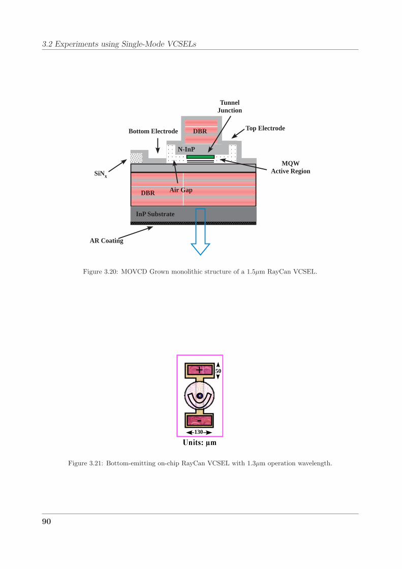
3.2 Experiments using Single-Mode VCSELs
DBR
DBR
N-InP
Bottom Electrode Top Electrode
AR Coating
Air Gap
InP Substrate
MQW Active Region
Tunnel Junction
SiNx
Figure 3.20: MOVCD Grown monolithic structure of a 1.5µm RayCan VCSEL.
50
130
+
-
Figure 3.21: Bottom-emitting on-chip RayCan VCSEL with 1.3µm operation wavelength.
90

Chapter 3 : Optical Injection-Locking Experiments
The VCSEL chip, integrated to the sub-mount is presented in figure 3.22. Integration to the
sub-mount provided solution to the above-discussed problems.
It allowed:
• The utilization of the VCSEL-chip in top-emitting configuration that in turn made
optical power collection using denuded single-mode and multimode optical fibers pos-
sible.
• The powering-up of the VCSEL-chip using 125 µm pitch GS probes already available
in the laboratory.
VC
SEL
A
NO
DE
VC
SEL
C
AT
HO
DE
80
50
250
450
130
120
150
Figure 3.22: 1.3µm RayCan VCSEL with sub-mount.
Furthermore, the intent of optical injection-locking experiments was observation of the
enhanced S21 response. This objective was compromised by the employment of the sub-
mount, as the S21 response was limited by the parasitic transmission line frequency. Figure.
3.23 presents the free-running S21 response of a 1.3 µm RayCan VCSEL. It is clear that
the resonance peak shifts toward higher frequencies with increasing bias currents but due
to the presence of parasitics, introduced by the sub-mount assembly, the cut-off frequency
does not increase significantly. The presence of air-gaps in the VCSEL structure implies
lower intrinsic cut-off frequencies. The inevitable utilization of the sub-mount assembly,
combined with the above-mentioned structural deficiency, render these VCSELs relatively
low frequency operation devices. It is perhaps due to this reason that the 10 Gbps modules
supplied by RayCan employ four VCSELs in parallel configuration to achieve 10Gbps bit
rate, as opposed to Vertilas 10Gbps modules that are composed of only one VCSEL.
91
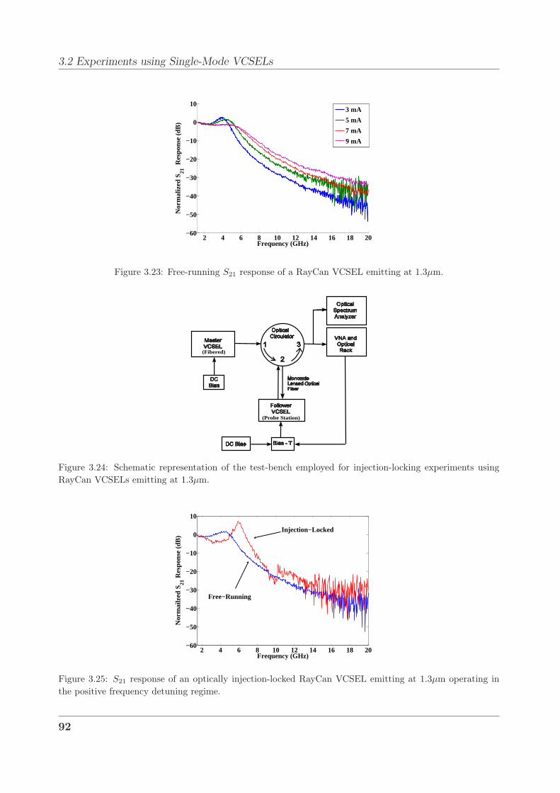
3.2 Experiments using Single-Mode VCSELs
2 4 6 8 10 12 14 16 18 20−60
−50
−40
−30
−20
−10
0
10
Frequency (GHz)
Nor
mal
ized
S21
Res
pons
e (d
B)
3 mA
5 mA
7 mA
9 mA
Figure 3.23: Free-running S21 response of a RayCan VCSEL emitting at 1.3µm.
(Fibered)
(Probe Station)
Figure 3.24: Schematic representation of the test-bench employed for injection-locking experiments using
RayCan VCSELs emitting at 1.3µm.
2 4 6 8 10 12 14 16 18 20−60
−50
−40
−30
−20
−10
0
10
Frequency (GHz)
Nor
mai
lzed
S21
Res
pons
e (d
B)
Free−Running
Injection−Locked
Figure 3.25: S21 response of an optically injection-locked RayCan VCSEL emitting at 1.3µm operating in
the positive frequency detuning regime.
92

Chapter 3 : Optical Injection-Locking Experiments
3.2.3.2 Injection Locking Experiments
The availability of fibered components however simplified the test-bench considerably. In
stead of using two probe-stations for master and follower VCSELs respectively, only one
probe-station was used since only the follower VCSEL was used in the on-chip configuration.
The utilization of a pigtailed master VCSEL also increased the available optical power and
allowed the elimination of the OSA from the injection-locking setup. Figure. 3.24 presents
the optical injection-locking test-bench used for RayCan VCSEL experiments schematically.
2 4 6 8 10 12 14 16 18 20−60
−50
−40
−30
−20
−10
0
10
Frequency (GHz)
Nor
mal
ized
S21
Res
pons
e (d
B)
Free−Running
Injection−Locked
Figure 3.26: S21 response of an optically injection-locked RayCan VCSEL emitting at 1.3µm operating in
the negative frequency detuning regime.
The utilization of a pigtailed master VCSEL made the test-bench considerably com-
pact and increased the available optical power but despite these advantages, the follower
VCSEL injection-locked S21 spectra do not exhibit very large resonance frequencies. Figure
3.25 presents the S21 response of an optically injection-locked RayCan follower VCSEL, in
the positive frequency detuning regime. Compared to the free-running responses presented
in figure 3.23, it is clear that an increased resonance frequency is observed. Also, due to
operation in the positive frequency detuning regime, the S21 is undamped and therefore the
resonance peak is very pronounced.
On the other hand, figure 3.26 presents the optically injection-locked RayCan follower
VCSEL S21 response in negative frequency detuning regime. The response is damped and the
resonance peaks are less prominent than the response given in figure 3.25. It must however be
noticed that due to the air-gap based structure, the optical injection-locked RayCan VCSEL
S21 responses do not exhibit resonance and cut-off frequencies as high as those obtained
using BeamExpress VCSELs and presented in Figures. 3.14, 3.15, 3.17 and 3.19.
93

3.3 Measurement Simulation Comparison
3.3 Measurement Simulation Comparison
We present the comparison between experimentally obtained S21 curves with the frequency
response curves obtained using the mathematical model explained in the preceding chapter.
Two important parameters of note, the frequency detuning (∆ω) and the injected photon
density (Sinj) have been varied in order to obtain the best-fit simulation curves. Figures 3.27,
3.28 and 3.29, give the comparison between measured and calculated frequency responses.
Table 3.1 summarizes the values of detuning frequency and injected photon density, used to
obtain the calculated S21 curves.
0 5 10 15 20−50
−40
−30
−20
−10
0
10
Frequency (GHz)
S 21 (
dB)
CalculatedMeasured
Figure 3.27: Comparison between the experimental and simulated S21 response of an optically injection-
locked BeamExpress VCSEL emitting at 1.3µm.
0 5 10 15 20−35
−30
−25
−20
−15
−10
−5
0
5
Frequency (GHz)
S 21 (
dB)
CalculatedMeasured
Figure 3.28: Comparison between the experimental and simulated S21 response of an optically injection-
locked BeamExpress VCSEL emitting at 1.3µm.
The difference at low frequencies, between the calculated and experimental curves, is
probably due to the insufficient injected optical power. During the experiments using on-chip
VCSELs, injecting sufficient amounts of optical powers into the lensed single-mode optical
fiber has consistently been identified as the most challenging aspect of the exercise.
94
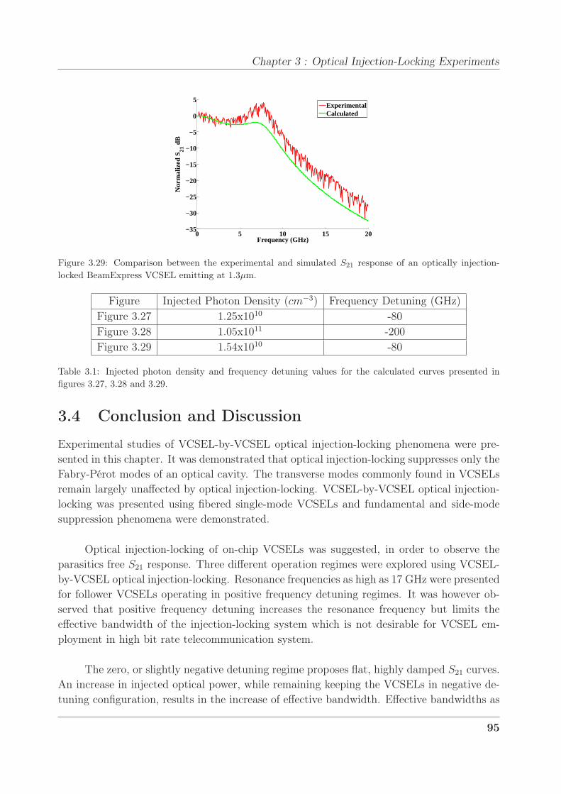
Chapter 3 : Optical Injection-Locking Experiments
0 5 10 15 20−35
−30
−25
−20
−15
−10
−5
0
5
Frequency (GHz)
Nor
mal
ized
S21
dB
ExperimentalCalculated
Figure 3.29: Comparison between the experimental and simulated S21 response of an optically injection-
locked BeamExpress VCSEL emitting at 1.3µm.
Figure Injected Photon Density (cm−3) Frequency Detuning (GHz)
Figure 3.27 1.25x10¹⁰ -80
Figure 3.28 1.05x10¹¹ -200
Figure 3.29 1.54x10¹⁰ -80
Table 3.1: Injected photon density and frequency detuning values for the calculated curves presented in
figures 3.27, 3.28 and 3.29.
3.4 Conclusion and Discussion
Experimental studies of VCSEL-by-VCSEL optical injection-locking phenomena were pre-
sented in this chapter. It was demonstrated that optical injection-locking suppresses only the
Fabry-Pérot modes of an optical cavity. The transverse modes commonly found in VCSELs
remain largely unaffected by optical injection-locking. VCSEL-by-VCSEL optical injection-
locking was presented using fibered single-mode VCSELs and fundamental and side-mode
suppression phenomena were demonstrated.
Optical injection-locking of on-chip VCSELs was suggested, in order to observe the
parasitics free S21 response. Three different operation regimes were explored using VCSEL-
by-VCSEL optical injection-locking. Resonance frequencies as high as 17 GHz were presented
for follower VCSELs operating in positive frequency detuning regimes. It was however ob-
served that positive frequency detuning increases the resonance frequency but limits the
effective bandwidth of the injection-locking system which is not desirable for VCSEL em-
ployment in high bit rate telecommunication system.
The zero, or slightly negative detuning regime proposes flat, highly damped S21 curves.
An increase in injected optical power, while remaining keeping the VCSELs in negative de-
tuning configuration, results in the increase of effective bandwidth. Effective bandwidths as
95

3.4 Conclusion and Discussion
high as 10 GHz, using optical injection-locking, have been demonstrated. It must be noted
that the free-running cut-off frequency of the VCSELs used is about 5 GHz.
In order to simplify the optical injection-locking setup, the utilization of a fibered
master VCSEL has been proposed. Such a configuration also increases the effective available
optical power. Optically injection-locked follower VCSEL S21 response has been presented
in different operating conditions. Experimental results and numerical calculations using the
mathematical model have been compared.
96

Chapter 3 : Optical Injection-Locking Experiments
Bibliography
[1] K. Iwashita and K. Nakagawa, “Suppression of Mode Partition Noise by Laser Diode
Light Injection,” Microwave Theory and Techniques, IEEE Transactions on, vol. 82,
no. 10, pp. 1657–1662, Oct 1982.
[2] A. Bacou, “Caractérisation et Modélisation optoélectronique de VCSEL à grande
longueur d’onde pour sous-ensembles optiques intégrés,” Ph.D. dissertation, Institut
Supérieur de l’Aéronautique et de l’Espace, 2008.
[3] C.-H. Chang, L. Chrostowski, and C. Chang-Hasnain, “Injection locking of VCSELs,”
IEEE Journal of Selected Topics in Quantum Electronics, vol. 9, no. 5, pp. 1386–1393,
Sept.-Oct. 2003.
[4] M.-R. Park, O.-K. Kwon, W.-S. Han, K.-H. Lee, S.-J. Park, and B.-S. Yoo, “All-epitaxial
InAlGaAs-InP VCSELs in the 1.3-1.6-µm Wavelength Range for CWDM Band Applica-
tions,” IEEE Photonics Technology Letters, vol. 18, no. 16, pp. 1717–1719, Aug. 2006.
97


Chap
ter
4 Frequency Response Extrac-
tion and RIN Measurements
Direct modulation is preferred in modern telecommunication systems in order to avoid the
costs presented by external modulators. Packaging and transmission line parasitics however
degrade the device performance and limit the high frequency response. To estimate the
VCSEL intrinsic frequency response, we have presented and utilized a rate equation based
model in precedent chapters. In effect, the same model can be employed to separate the in-
trinsic device response from the overall observed packaged system response. The procedure
is denoted as “Frequency Response Subtraction” and would be treated extensively here.
The second half of this chapter deals with RIN measurements of fibered free-running and
injection-locked VCSELs. RIN variation as function of wavelength detuning is observed. A
RIN improvement of about 10 dB is reported under injection-locking conditions.
4.1 Frequency Response Subtraction
Modulation of on-chip VCSELs allows us to observe the intrinsic frequency response but
coupling optical power from the VCSEL into a single-mode denuded fiber can prove to be
challenging. Modulation of fibered VCSELs allows to work with sufficiently high power
levels but the packaging parasitics hinder the observation of intrinsic response. A technique
has been proposed [1] to extract the intrinsic frequency response of a DFB laser using S21
measurements and the device mathematical model. A comprehensive mathematical model
for long wavelength VCSELs was developed by A. Bacou and is presented in [2].
4.1.1 Extraction Procedure
The basic concept of the extraction procedure can be summarized as follows:
• By subtracting the S21 response for a bias current just above the threshold, from
the S21 responses well above the threshold, the parasitic influences can effectively be
eliminated since the result of the subtraction depends only on the bias current related
S21 response variation.
• A mathematical model is defined and the subtraction procedure is repeated to obtain
calculated S21 curves similar to those obtained experimentally.
99

4.1 Frequency Response Subtraction
• The experimentally obtained curves are fitted to the calculated curves by varying the
mathematical model parameters.
• The S21 curves are reconstructed using the mathematical model parameters obtained
after fitting.
4.1.1.1 Mathematical Model
The VCSEL resonance frequency response fr can be expressed in terms of variables Y and Z
that in turn depend upon VCSEL intrinsic parameters. Y corresponds to the laser frequency
response damping factor and along with Z can be used to estimate the laser resonance
frequency. Y and Z can be expressed mathematically as follows [1],
Y = vga0S
1 + ǫS+
1
τe
− Γvga0(Nth − Ntr)1
(1 + ǫS)2+
1
τP
(4.1)
Z = vga0S
1 + ǫS
1
τP
+ (β − 1)Γvga0
τN
(Nth − Ntr)1
(1 + ǫS)2+
1
τeτP
(4.2)
Where Nth and Ntr are the electron threshold and transparency densities, a0 the dif-
ferential gain coefficient, S the photon density, vg the group velocity, β the spontaneous
emission coefficient and Γ the confinement factor. τN and τP are the the carrier and photon
lifetimes respectively.
The system transfer function H(f) and the resonance frequency fr can be expressed in
terms of Y and Z as follows:
fr =1
2π
√Z − 0.5Y 2 (4.3)
H(f) =fr
2
(fr2 − f 2) + jfY π
2
(4.4)
The transfer function of a VCSEL can therefore be calculated using the parameters
presented in Table. 4.1.
Figure 4.1 presents the calculated normalized S21 response of a VCSEL, using the
intrinsic parameters given in Table.4.1.
4.1.1.2 Experimental Results
The devices used are fibered, single-mode RayCan VCSELs emitting at 1.3µm wavelength.
The experimentally obtained S21 curves for different bias currents have been presented in
Fig. 4.2. The packaging cut-off frequency is about 4 GHz. The intrinsic response up to 4
GHz (i.e. for the bias current values of 3mA and 4mA) can be easily observed. S21 response
100

Chapter 4 : Frequency Response Extraction and RIN Measurements
Parameter Units Value
τN ns 0.61
Nth cm−3 5.33x10¹⁸
Ntr cm−3 3.24x10¹⁸
a0 cm2 4.8x10⁻¹⁶
vg cm/s 7.7x10⁹
ǫ cm3 2.2x10⁻¹⁷
τP ps 6.4
S cm−3 2.5x10¹⁵
Table 4.1: Long wavelength VCSEL intrinsic parameters used to simulate the small-signal [3].
0 5 10 15 20−30
−25
−20
−15
−10
−5
0
5
10
Frequency (GHz)
Nor
mal
ized
S21
(dB
)
4 mA5 mA6 mA7 mA8 mA9 mA
Figure 4.1: Calculated S21 response curves for different bias currents.
101
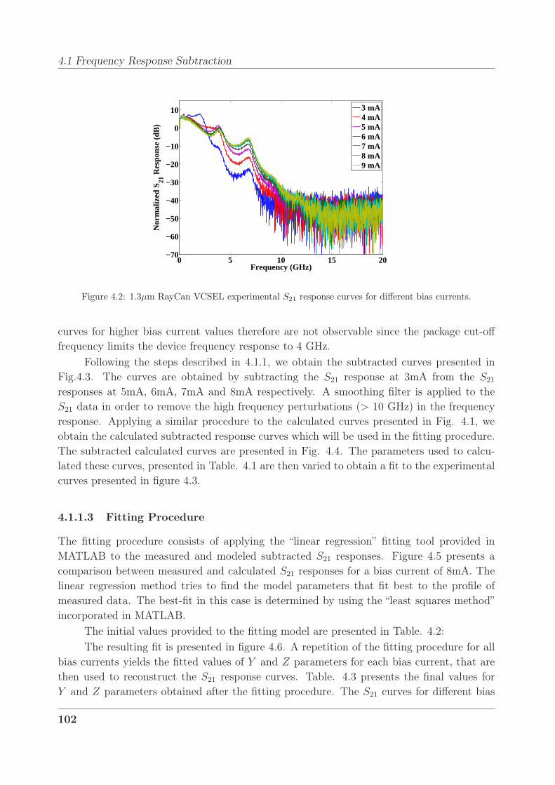
4.1 Frequency Response Subtraction
0 5 10 15 20−70
−60
−50
−40
−30
−20
−10
0
10
Frequency (GHz)
Nor
mal
ized
S21
Res
pons
e (d
B)
3 mA4 mA5 mA6 mA7 mA8 mA9 mA
Figure 4.2: 1.3µm RayCan VCSEL experimental S21 response curves for different bias currents.
curves for higher bias current values therefore are not observable since the package cut-off
frequency limits the device frequency response to 4 GHz.
Following the steps described in 4.1.1, we obtain the subtracted curves presented in
Fig.4.3. The curves are obtained by subtracting the S21 response at 3mA from the S21
responses at 5mA, 6mA, 7mA and 8mA respectively. A smoothing filter is applied to the
S21 data in order to remove the high frequency perturbations (> 10 GHz) in the frequency
response. Applying a similar procedure to the calculated curves presented in Fig. 4.1, we
obtain the calculated subtracted response curves which will be used in the fitting procedure.
The subtracted calculated curves are presented in Fig. 4.4. The parameters used to calcu-
lated these curves, presented in Table. 4.1 are then varied to obtain a fit to the experimental
curves presented in figure 4.3.
4.1.1.3 Fitting Procedure
The fitting procedure consists of applying the “linear regression” fitting tool provided in
MATLAB to the measured and modeled subtracted S21 responses. Figure 4.5 presents a
comparison between measured and calculated S21 responses for a bias current of 8mA. The
linear regression method tries to find the model parameters that fit best to the profile of
measured data. The best-fit in this case is determined by using the “least squares method”
incorporated in MATLAB.
The initial values provided to the fitting model are presented in Table. 4.2:
The resulting fit is presented in figure 4.6. A repetition of the fitting procedure for all
bias currents yields the fitted values of Y and Z parameters for each bias current, that are
then used to reconstruct the S21 response curves. Table. 4.3 presents the final values for
Y and Z parameters obtained after the fitting procedure. The S21 curves for different bias
102

Chapter 4 : Frequency Response Extraction and RIN Measurements
0 2 4 6 8 10
−4
−2
0
2
4
6
8
10
12
Frequency (GHz)
Sub
trac
ted
Exp
erim
enta
l S21
(dB
)
5 mA6 mA7 mA8 mA
Figure 4.3: 1.3µm RayCan VCSEL subtracted experimental S21 response curves for different bias currents.
0 2 4 6 8 10−25
−20
−15
−10
−5
0
5
10
15
Frequency (GHz)
Sub
trac
ted
Cal
cula
ted
S 21
5 mA6 mA7 mA8 mA
Figure 4.4: 1.3µm RayCan VCSEL subtracted calculated S21 response curves for different bias currents.
Parameter Value
Y4mA 1.057x10⁹
Z4mA 5.03x10²⁰
Y5mA 5.16x10⁹
Z5mA 8.13x10²⁰
Table 4.2: Initial values used to calculate the best-fit between calculated and experimental curves.
103
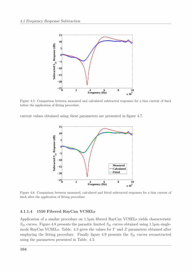
4.1 Frequency Response Subtraction
0 2 4 6 8 10x 10
9
−25
−20
−15
−10
−5
0
5
10
15
Frequency (Hz)
Sub
trac
ted
S 21 R
espo
nse
(dB
)
Figure 4.5: Comparison between measured and calculated subtracted responses for a bias current of 8mA
before the application of fitting procedure.
current values obtained using these parameters are presented in figure 4.7.
0 2 4 6 8 10x 10
9
−25
−20
−15
−10
−5
0
5
10
15
Frequency (Hz)
Sub
trac
ted
S 21 R
espo
nse
(dB
)
MeasuredCalculatedFitted
Figure 4.6: Comparison between measured, calculated and fitted subtracted responses for a bias current of
8mA after the application of fitting procedure.
4.1.1.4 1550 Fibered RayCan VCSELs
Application of a similar procedure on 1.5µm fibered RayCan VCSELs yields characteristic
S21 curves. Figure 4.8 presents the parasitic limited S21 curves obtained using 1.5µm single-
mode RayCan VCSELs. Table. 4.3 gives the values for Y and Z parameters obtained after
employing the fitting procedure. Finally figure 4.9 presents the S21 curves reconstructed
using the parameters presented in Table. 4.3.
104

Chapter 4 : Frequency Response Extraction and RIN Measurements
Current Y(1.3µm) Z(1.3µm) Y(1.5µm) Z(1.5µm)
5 mA 1.30x10¹⁰ 7.5x10²⁰ 9.16x10⁹ 3.4x10²⁰
6 mA 1.60x10¹⁰ 9.7x10²⁰ 1.17x10¹⁰ 4.5x10²⁰
7 mA 1.79x10¹⁰ 1.15x10²¹ 1.73x10¹⁰ 5.21x10²¹
8 mA 2.10x10¹⁰ 1.35x10²¹ 1.49x10¹⁰ 6.68x10²¹
Table 4.3: Final values of Y and Z parameters for different bias currents after the fitting procedure.
0 2 4 6 8 10−15
−10
−5
0
5
10
Frequency (GHz)
Fitt
ed S
21 R
espo
nse
(dB
)
5 mA6 mA7 mA8 mA
Figure 4.7: Reconstructed S21 response curves using the Y and Z values presented in Table. 4.3.
0 2 4 6 8 10
−50
−40
−30
−20
−10
0
Frequency (GHz)
Nor
mal
ized
S21
Res
pons
e (d
B)
4 mA5 mA6 mA7 mA8mA9 mA
Figure 4.8: 1.5µm RayCan VCSEL experimental S21 response curves for different bias currents.
105
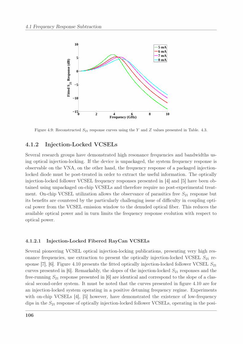
4.1 Frequency Response Subtraction
0 2 4 6 8 10−15
−10
−5
0
5
10
Frequency (GHz)
Fitt
ed S
21 R
espo
nse
(dB
)
5 mA6 mA7 mA8 mA
Figure 4.9: Reconstructed S21 response curves using the Y and Z values presented in Table. 4.3.
4.1.2 Injection-Locked VCSELs
Several research groups have demonstrated high resonance frequencies and bandwidths us-
ing optical injection-locking. If the device is unpackaged, the system frequency response is
observable on the VNA, on the other hand, the frequency response of a packaged injection-
locked diode must be post-treated in order to extract the useful information. The optically
injection-locked follower VCSEL frequency responses presented in [4] and [5] have been ob-
tained using unpackaged on-chip VCSELs and therefore require no post-experimental treat-
ment. On-chip VCSEL utilization allows the observance of parasitics free S21 response but
its benefits are countered by the particularly challenging issue of difficulty in coupling opti-
cal power from the VCSEL emission window to the denuded optical fiber. This reduces the
available optical power and in turn limits the frequency response evolution with respect to
optical power.
4.1.2.1 Injection-Locked Fibered RayCan VCSELs
Several pioneering VCSEL optical injection-locking publications, presenting very high res-
onance frequencies, use extraction to present the optically injection-locked VCSEL S21 re-
sponse [7], [6]. Figure 4.10 presents the fitted optically injection-locked follower VCSEL S21
curves presented in [6]. Remarkably, the slopes of the injection-locked S21 responses and the
free-running S21 response presented in [6] are identical and correspond to the slope of a clas-
sical second-order system. It must be noted that the curves presented in figure 4.10 are for
an injection-locked system operating in a positive detuning frequency regime. Experiments
with on-chip VCSELs [4], [5] however, have demonstrated the existence of low-frequency
dips in the S21 response of optically injection-locked follower VCSELs, operating in the posi-
106
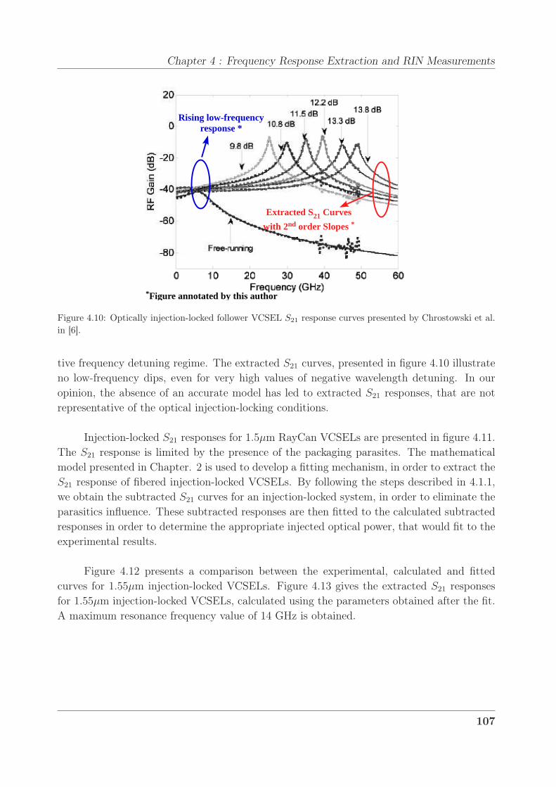
Chapter 4 : Frequency Response Extraction and RIN Measurements
Extracted S21 Curves
with 2nd order Slopes *
*Figure annotated by this author
Rising low-frequency response *
Figure 4.10: Optically injection-locked follower VCSEL S21 response curves presented by Chrostowski et al.
in [6].
tive frequency detuning regime. The extracted S21 curves, presented in figure 4.10 illustrate
no low-frequency dips, even for very high values of negative wavelength detuning. In our
opinion, the absence of an accurate model has led to extracted S21 responses, that are not
representative of the optical injection-locking conditions.
Injection-locked S21 responses for 1.5µm RayCan VCSELs are presented in figure 4.11.
The S21 response is limited by the presence of the packaging parasites. The mathematical
model presented in Chapter. 2 is used to develop a fitting mechanism, in order to extract the
S21 response of fibered injection-locked VCSELs. By following the steps described in 4.1.1,
we obtain the subtracted S21 curves for an injection-locked system, in order to eliminate the
parasitics influence. These subtracted responses are then fitted to the calculated subtracted
responses in order to determine the appropriate injected optical power, that would fit to the
experimental results.
Figure 4.12 presents a comparison between the experimental, calculated and fitted
curves for 1.55µm injection-locked VCSELs. Figure 4.13 gives the extracted S21 responses
for 1.55µm injection-locked VCSELs, calculated using the parameters obtained after the fit.
A maximum resonance frequency value of 14 GHz is obtained.
107

4.1 Frequency Response Subtraction
0 5 10 15 20 25 30 35 40−60
−50
−40
−30
−20
−10
0
10
20
Freqeuncy (GHz)
Nor
mal
ized
S21
(dB
)
5.5 dBm6.0 dBm6.5 dBm7.0 dBm7.5 dBm
Figure 4.11: RayCan 1.5µm optically injection-locked follower VCSEL S21 response curves for different
incident optical powers.
0 5 10 15 20 25 30 35 40−10
−5
0
5
10
15
Frequency (GHz)
Sub
trac
ted
S 21 R
espo
nse
(dB
)
OrigStartEnd
Figure 4.12: Subtracted calculated optically injection-locked follower VCSEL S21 response curves for different
incident optical powers.
108
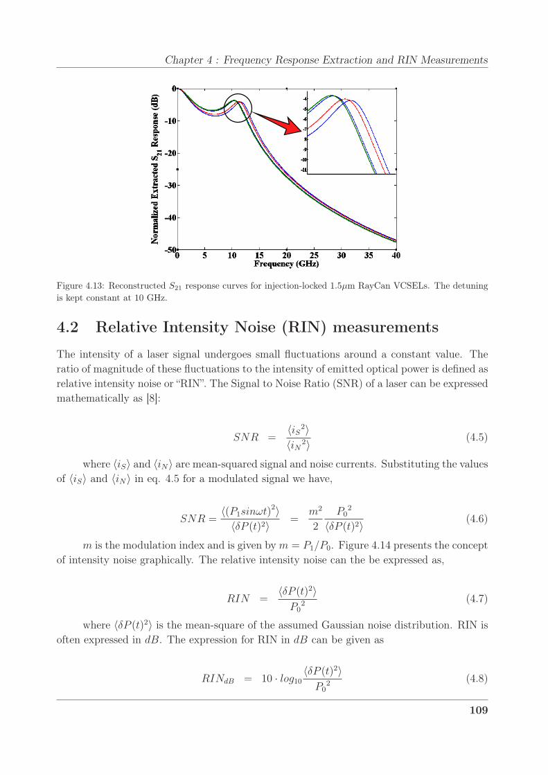
Chapter 4 : Frequency Response Extraction and RIN Measurements
Figure 4.13: Reconstructed S21 response curves for injection-locked 1.5µm RayCan VCSELs. The detuning
is kept constant at 10 GHz.
4.2 Relative Intensity Noise (RIN) measurements
The intensity of a laser signal undergoes small fluctuations around a constant value. The
ratio of magnitude of these fluctuations to the intensity of emitted optical power is defined as
relative intensity noise or “RIN”. The Signal to Noise Ratio (SNR) of a laser can be expressed
mathematically as [8]:
SNR =〈iS2〉〈iN 2〉 (4.5)
where 〈iS〉 and 〈iN〉 are mean-squared signal and noise currents. Substituting the values
of 〈iS〉 and 〈iN〉 in eq. 4.5 for a modulated signal we have,
SNR =〈(P1sinωt)2〉〈δP (t)2〉 =
m2
2
P02
〈δP (t)2〉 (4.6)
m is the modulation index and is given by m = P1/P0. Figure 4.14 presents the concept
of intensity noise graphically. The relative intensity noise can the be expressed as,
RIN =〈δP (t)2〉
P02 (4.7)
where 〈δP (t)2〉 is the mean-square of the assumed Gaussian noise distribution. RIN is
often expressed in dB. The expression for RIN in dB can be given as
RINdB = 10 · log10〈δP (t)2〉
P02 (4.8)
109

4.2 Relative Intensity Noise (RIN) measurements
0 100 200 300 400 500−1
−0.5
0
0.5
1
1.5
2
Time (A.U.)
P(t
) (A
.U.)
Noisy SignalIdeal Signal
P(t) = P0+ P
1sin ωt + δP(t)
⟨ δ P(t)2 ⟩0.5
P0
P1
Figure 4.14: Example of noise in modulated laser signal for analog applications.
The test bench utilized for RIN measurements of free-running RayCan VCSELs emit-
ting at 1.55µm is presented in figure 4.15. The fibered VCSELs are powered-up using a
stable KEITHLEY DC power supply. The output optical power is converted into electrical
power using a Lasertron high speed photodiode. The electrical output is amplified using a
transimpedance amplifier and fed to the electrical spectrum analyzer.
Electrical Spectrum Analyzer
Amperemeter
Transimpedence Amplifier
VCSEL
DC Optical Fibre
PD
Figure 4.15: Testbench for RIN measurements of 1.5µm free-running Raycan VCSELs
The RIN of a laser diode is then calculated using the following mathematical expression:
RIN =
PObs−PAnalyzer
G− 2qIPDRLoad
IPD2RLoad
(4.9)
where,
• PObs is the optical power observed on the electrical spectrum analyzer
• PAnalyzer is the electrical spectrum analyzer noise floor power
• RLoad is the electrical spectrum analyzer load resistance
110

Chapter 4 : Frequency Response Extraction and RIN Measurements
• IPD is the photo diode current
• G is the transimpedance amplifier gain, and
• q is the electron charge
Since a photodiode is used for the O/E conversion, the photodiode shot noise con-
tribution to the VCSEL RIN measurement must be taken into account. The expression
2qIPDRLoad is the photodiode shot noise which must be subtracted from the VCSEL output
power fluctuations before the RIN calculation. The PAnalyzer comprises of the electircal spec-
trum analyzer noise floor which is defined by the intrinsic thermal noise of the instrument.
The typical value of the noise floor power for the instrument used in these experiments is
about -165dB/Hz. This value imposes a limit on the VCSEL observable noise and therefore
noise level below this threshold can not be measured. Since typical VCSEL RIN values are
found in the 145-150 dB/Hz range, this instrument noise floor value is sufficient enough to
carry-out the RIN-related experiments. The RIN measurements of a 1.55µm free-running
RayCan VCSEL are presented in figure 4.16.
10−1
100
101
−150
−145
−140
−135
−130
Frequency (GHz)
RIN
(dB
/Hz)
4mA5mA6mA7mA8mA9mA
Figure 4.16: RIN measurements for a 1.55µm RayCan VCSEL for different bias currents.
The RIN measurements presented in figure 4.16 show the intrinsic resonance frequency
peak of the VCSEL. They also give the intrinsic relaxation oscillation frequency’s evolution
with respect to increasing bias current. The resonance frequency increases with increasing
bias current while the resonance peak damping is more pronounced with increasing bias cur-
rents. Since RIN measurements do not involve direct RF modulation of lasers, the problems
associated with modulation frequency related parasitics are automatically eliminated. RIN
curves serve therefore as excellent estimates of the intrinsic direct modulation bandwidths
of lasers. The highest value of resonance frequency for the VCSELs under test is found to
111

4.2 Relative Intensity Noise (RIN) measurements
0.2 0.3 0.4 0.5 0.6 0.7 0.8 0.9 1−150
−145
−140
−135
−130
−125
log10
(I−Ith
)
RIN
Max
(dB
/Hz)
RIN
Max = − 21 log
10(I−I
th) − 132
Figure 4.17: Peak RIN plotted as a function of increasing bias current. The black dots signify the peak RINs
for different bias currents, while the solid red line is the mathematical fit.
be about 6 GHz. Equation 4.7 shows that for increasing optical output powers, the RIN de-
creases. Figure 4.16 demonstrates a decrease from -146 dB/Hz to -150 dB/Hz as a function
of increasing bias currents.
The RIN dependence on laser bias current for conventional EELs can be mathematically
characterized as [8]:
RIN(fR) ∝ (Ibias − Ith)−3 (4.10)
In order to compare the VCSEL RIN peak bias current dependence,to that of the EELs,
the RIN is plotted against log10(Ibias − Ith)1. The resulting plot is presented in figure 4.17
The equation for the linear fit of this plot is
RINMax = −21log10(Ibias − Ith) − 132 (4.11)
From equation 4.11, it can be deduced that the slope is -21, which when converted to
linear scale results in:
RIN(fR) ∝ (Ibias − Ith)−2 (4.12)
which demonstrates that the VCSEL RIN decays slowly as compared to EEL RIN
and the difference of order between the two respective decays is 1. This can be explained
1Since the RIN is generally measured and expressed in dB/Hz, for the reason of being consistent, it is
plotted as the logarithm of the difference between the bias and threshold currents.
112
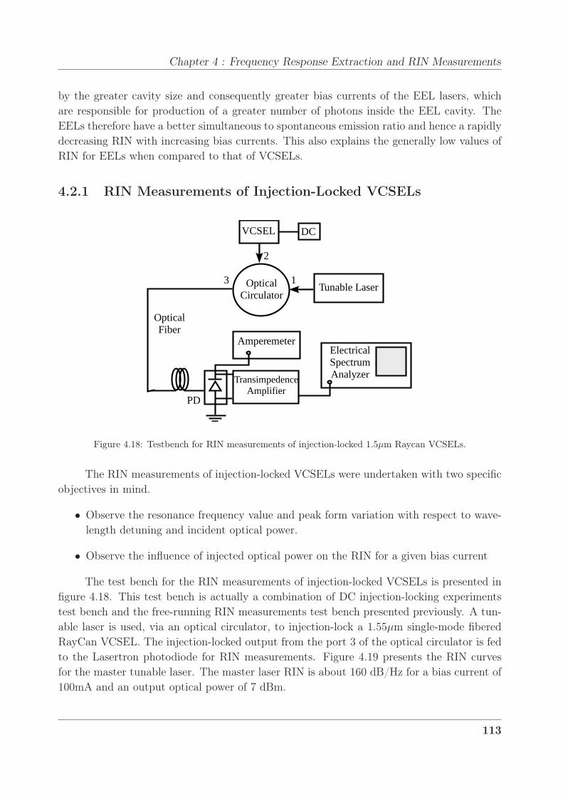
Chapter 4 : Frequency Response Extraction and RIN Measurements
by the greater cavity size and consequently greater bias currents of the EEL lasers, which
are responsible for production of a greater number of photons inside the EEL cavity. The
EELs therefore have a better simultaneous to spontaneous emission ratio and hence a rapidly
decreasing RIN with increasing bias currents. This also explains the generally low values of
RIN for EELs when compared to that of VCSELs.
4.2.1 RIN Measurements of Injection-Locked VCSELs
Optical Circulator
Transimpedence Amplifier
VCSEL DC
Amperemeter
PD
Optical Fiber
1
2
3
Electrical Spectrum Analyzer
Tunable Laser
Figure 4.18: Testbench for RIN measurements of injection-locked 1.5µm Raycan VCSELs.
The RIN measurements of injection-locked VCSELs were undertaken with two specific
objectives in mind.
• Observe the resonance frequency value and peak form variation with respect to wave-
length detuning and incident optical power.
• Observe the influence of injected optical power on the RIN for a given bias current
The test bench for the RIN measurements of injection-locked VCSELs is presented in
figure 4.18. This test bench is actually a combination of DC injection-locking experiments
test bench and the free-running RIN measurements test bench presented previously. A tun-
able laser is used, via an optical circulator, to injection-lock a 1.55µm single-mode fibered
RayCan VCSEL. The injection-locked output from the port 3 of the optical circulator is fed
to the Lasertron photodiode for RIN measurements. Figure 4.19 presents the RIN curves
for the master tunable laser. The master laser RIN is about 160 dB/Hz for a bias current of
100mA and an output optical power of 7 dBm.
113

4.2 Relative Intensity Noise (RIN) measurements
10−1
100
101
−160
−155
−150
−145
−140
Frequency (GHz)
RIN
(dB
/Hz)
50mA60mA70mA80mA90mA100mA120mA
Figure 4.19: Tunable laser RIN curves for various bias currents
In previous chapters, we have discussed the frequency response of injection-locked
VCSELs operating in positive or negative wavelength detuning regimes. As the resonance
frequency of an injection-locked system increases, so does the complexity of a test bench,
realized to observe the injection-locked follower VCSEL’s S21 response. In case of fibered
components, the parasitic limitations oblige us to utilize extraction techniques (developed
and presented in preceding sections), for the observation of S21 response . RIN measurements
however can be employed to observe the detuning response of an injection-locked system as
the VCSEL is not modulated and works in the so called “Static” operating conditions.
4.2.1.1 Negative Wavelength Detuning Regime
Figure 4.20 presents the RIN of an injection-locked VCSEL under various injection-powers.
A bias current of 5 mA has been maintained throughout this series of measurements, in
order to eliminate the bias current dependent damping of RIN curves. The VCSELs are
injection-locked at the negative wavelength detuning edge of the locking range.
The generation of high frequency beat notes, as a resulting of positive frequency de-
tuning, inside the VCSEL optical cavity, results in an under-damped response. The injected
optical power increases the effective locking-range which allows to sustain high values of
∆ω = ωMaster − ωFollower and hence high values of resonance frequency. The resonance fre-
quency observed in figure 4.20 increases from 6 GHz to about 12 GHz under the influence of
increasing optical power and detuning.
114
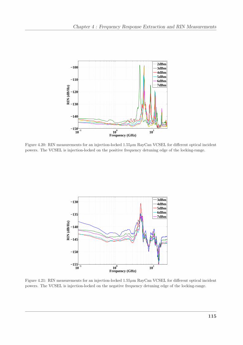
Chapter 4 : Frequency Response Extraction and RIN Measurements
10−1
100
101−150
−140
−130
−120
−110
−100
Frequency (GHz)
RIN
(dB
/Hz)
2dBm3dBm4dBm5dBm6dBm7dBm
Figure 4.20: RIN measurements for an injection-locked 1.55µm RayCan VCSEL for different optical incident
powers. The VCSEL is injection-locked on the positive frequency detuning edge of the locking-range.
10−1
100
101−155
−150
−145
−140
−135
−130
Frequency (GHz)
RIN
(dB
/Hz)
3dBm4dBm5dBm6dBm7dBm
Figure 4.21: RIN measurements for an injection-locked 1.55µm RayCan VCSEL for different optical incident
powers. The VCSEL is injection-locked on the negative frequency detuning edge of the locking-range.
115
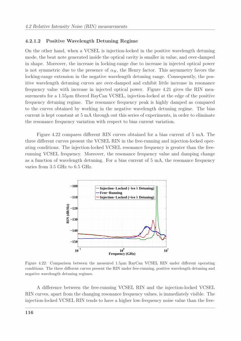
4.2 Relative Intensity Noise (RIN) measurements
4.2.1.2 Positive Wavelength Detuning Regime
On the other hand, when a VCSEL is injection-locked in the positive wavelength detuning
mode, the beat note generated inside the optical cavity is smaller in value, and over-damped
in shape. Moreover, the increase in locking-range due to increase in injected optical power
is not symmetric due to the presence of αH , the Henry factor. This asymmetry favors the
locking-range extension in the negative wavelength detuning range. Consequently, the pos-
itive wavelength detuning curves are over-damped and exhibit little increase in resonance
frequency value with increase in injected optical power. Figure 4.21 gives the RIN mea-
surements for a 1.55µm fibered RayCan VCSEL, injection-locked at the edge of the positive
frequency detuning regime. The resonance frequency peak is highly damped as compared
to the curves obtained by working in the negative wavelength detuning regime. The bias
current is kept constant at 5 mA through out this series of experiments, in order to eliminate
the resonance frequency variation with respect to bias current variation.
Figure 4.22 compares different RIN curves obtained for a bias current of 5 mA. The
three different curves present the VCSEL RIN in the free-running and injection-locked oper-
ating conditions. The injection-locked VCSEL resonance frequency is greater than the free-
running VCSEL frequency. Moreover, the resonance frequency value and damping change
as a function of wavelength detuning. For a bias current of 5 mA, the resonance frequency
varies from 3.5 GHz to 6.5 GHz.
10−1
100
101
−150
−140
−130
−120
−110
−100
Frequency (GHz)
RIN
(dB
/Hz)
Injection−Locked (−ive λ Detuning) Free−RunningInjection−Locked (+ive λ Detuning)
Figure 4.22: Comparison between the measured 1.5µm RayCan VCSEL RIN under different operating
conditions. The three different curves present the RIN under free-running, positive wavelength detuning and
negative wavelength detuning regimes.
A difference between the free-running VCSEL RIN and the injection-locked VCSEL
RIN curves, apart from the changing resonance frequency values, is immediately visible. The
injection-locked VCSEL RIN tends to have a higher low-frequency noise value than the free-
116

Chapter 4 : Frequency Response Extraction and RIN Measurements
running VCSEL RIN. Two different explanations can be proposed for this phenomenon. As
Sciamanna et al. have demonstrated that this might be due to the transvers-mode switching
phenomenon visible in the optically injection-locked VCSELs [9], [10]. On the other hand, the
optically injection-locked VCSEL RIN resemebles that of a multimode VCSEL which, due
to mode competition, has a higher RIN at lower frequencies. The frequency-beating inside
the single-mode injection-locked VCSEL optical cavity might be regarded as analogous to
a multimode VCSEL cavity with mode competition resulting in an increased RIN at lower
frequencies.
4.2.1.3 RIN Improvement
RIN improvement under optical injection-locking has been demonstrated previously by dif-
ferent research groups [11], [12]. The comparison between free-running and injection-locked
spectra of a 1.55µm RayCan VCSEL are presented in figure 4.23. The RIN reduction is
observed due to increased resonance frequency.
100
101
−150
−140
−130
−120
−110
−100
Frequency (GHz)
RIN
(dB
/Hz)
Free− Running Injection−Locked
10 dB
Figure 4.23: Comparison between the free-running and injection-locked 1.5µm RayCan VCSEL RIN spectra.
In other words, the low frequency (1-5 GHz) RIN improves because under the injection-
locking influence, the noise peak shifts toward high frequencies, thus removing the effects of
high RIN under the normal free-running conditions. The reduction of RIN can be explained
qualitatively as well as quantitatively. Qualitatively speaking, under injection-locking con-
ditions, fewer carriers are needed to achieve simultaneous emission and lasing action. The
spontaneous emission contribution of the laser is lessened, hence reducing the noise. Mathe-
matically, this phenomenon can be explained as increase in the value of P02 in the equation
4.7, which has the effect of producing a diminished RIN measurement.
It must be noted however that when the term “RIN improvement using optical injection-
locking”is employed, it effectively means the shifting of peak RIN to higher frequencies.
117
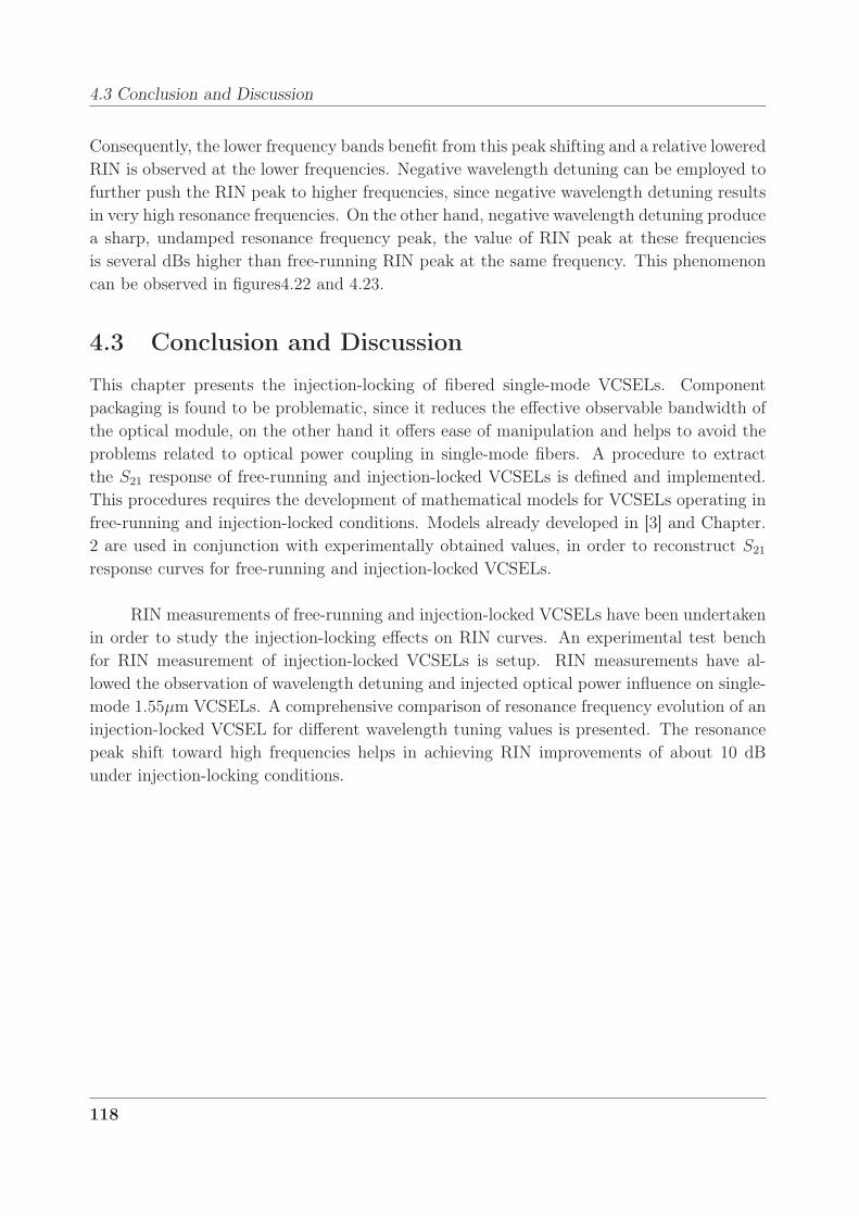
4.3 Conclusion and Discussion
Consequently, the lower frequency bands benefit from this peak shifting and a relative lowered
RIN is observed at the lower frequencies. Negative wavelength detuning can be employed to
further push the RIN peak to higher frequencies, since negative wavelength detuning results
in very high resonance frequencies. On the other hand, negative wavelength detuning produce
a sharp, undamped resonance frequency peak, the value of RIN peak at these frequencies
is several dBs higher than free-running RIN peak at the same frequency. This phenomenon
can be observed in figures4.22 and 4.23.
4.3 Conclusion and Discussion
This chapter presents the injection-locking of fibered single-mode VCSELs. Component
packaging is found to be problematic, since it reduces the effective observable bandwidth of
the optical module, on the other hand it offers ease of manipulation and helps to avoid the
problems related to optical power coupling in single-mode fibers. A procedure to extract
the S21 response of free-running and injection-locked VCSELs is defined and implemented.
This procedures requires the development of mathematical models for VCSELs operating in
free-running and injection-locked conditions. Models already developed in [3] and Chapter.
2 are used in conjunction with experimentally obtained values, in order to reconstruct S21
response curves for free-running and injection-locked VCSELs.
RIN measurements of free-running and injection-locked VCSELs have been undertaken
in order to study the injection-locking effects on RIN curves. An experimental test bench
for RIN measurement of injection-locked VCSELs is setup. RIN measurements have al-
lowed the observation of wavelength detuning and injected optical power influence on single-
mode 1.55µm VCSELs. A comprehensive comparison of resonance frequency evolution of an
injection-locked VCSEL for different wavelength tuning values is presented. The resonance
peak shift toward high frequencies helps in achieving RIN improvements of about 10 dB
under injection-locking conditions.
118
Chapter 4 : Frequency Response Extraction and RIN Measurements
Bibliography
[1] J. Cartledge and R. Srinivasan, “Extraction of DFB laser rate equation parameters
for system simulation purposes,” Journal of Lightwave Technology, vol. 15, no. 5, pp.
852–860, May 1997.
[2] Bacou, A. and Hayat, A. and Rissons, A. and Iakovlev, V. and Syrbu, A. and Mollier, J.-
C. and Kapon, E., “VCSEL Intrinsic Response Extraction Using T-Matrix Formalism,”
IEEE Photonics Technology Letters, vol. 21, no. 14, pp. 957–959, July15, 2009.
[3] A. Bacou, “Caractérisation et Modélisation optoélectronique de VCSEL à grande
longueur d’onde pour sous-ensembles optiques intégrés,” Ph.D. dissertation, Institut
Supérieur de l’Aéronautique et de l’Espace, 2008.
[4] A. Hayat, A. Bacou, A. Rissons, J.-C. Mollier, V. Iakovlev, A. Syrbu, and E. Kapon,
“Long Wavelength VCSEL-by-VCSEL Optical Injection Locking,” Accepted for publica-
tion in IEEE Transactions on Microwave Theory and Techniques, 2009.
[5] ——, “1.3µm single-mode VCSEL-by-VCSEL optical injection-locking for enhanced mi-
crowave performance,” in 21st Annual Meeting of the IEEE Lasers and Electro-Optics
Society,2008. LEOS 2008., Nov. 2008, pp. 224–225.
[6] L. Chrostowski, X. Zhao, C. Chang-Hasnian, R. Shau, M. Ortsiefer, and M.-C.
Amann, “Very High Resonance Frequency (>40 GHz) Optical Injection-Locked 1.55 µm
VCSELs,” in IEEE International Topical Meeting on Microwave Photonics. MWP’04.,
4-6 Oct. 2004, pp. 255 – 258.
[7] L. Chrostowski, X. Zhao, and C. Chang-Hasnain, “Microwave Performance of Optically
Injection-locked VCSELs,” IEEE Transactions on Microwave Theory and Techniques,
vol. 54, no. 2, pp. 788–796, Feb. 2006.
[8] L. Coldren and S. Corzine, Diode Lasers and Photonic Integrated Circuits, K. Chang,
Ed. John Wiley & Sons. Inc., 1995.
[9] I. Gatare, M. Sciamanna, A. Locquet and K. Panajotov, “Influence of polarization
mode competition on the synchronization of two unidirectionally coupled vertical-cavity
surface-emitting lasers,” Optics Letters, vol. 32, pp. 1629–1631 no. 12, 2007.
[10] I. Gatare, M. Sciamanna, A. Locquet and K. Panajotov, “Transverse Mode Switching
and Locking in Vertica-Cavity Surface-Emitting Lasers Subject to Orthogonal Injec-
tion,” IEEE Photonics Technology Letters, vol. 43, no. 4, pp. 322–333, 2007.
[11] L. Chrostowski, C.-H. Chang, and C. Chang-Hasnain, “Reduction of Relative Intensity
Noise and Improvement of Spur-Free Dynamic Range of an Injection-Locked VCSEL,”
The 16th Annual Meeting of the IEEE Lasers and Electro-Optics Society. LEOS 2003.,
vol. 2, pp. 706–707 vol.2, Oct. 2003.
119

BIBLIOGRAPHY
[12] X. Jin and S. L. Chuang, “Relative intensity noise characteristics of injection-locked
semiconductor lasers,” Applied Physics Letters, vol. 77, no. 9, pp. 1250–1252, 2000.
120

Conclusion and Future Prospects
The research work presented here is carried-out in the context of a trans-national project,
in partnership with Ecole Polytechnique Fédérale de Lausanne (EPFL), BeamExpress ( an
EPFL spin-off) and D-Lightsys, a French company specializing in optical interconnects for
harsh environments 2. The project focus is on conception of optical sub-assemblies for de-
ployment in 10Gbps links using 1.3µm and 1.5µm VCSELs. Three distinct functionalities
namely, fabrication, characterization and product development are attributed respectively
to EPFL/BeamExpress, MOSE-ISAE and D-Light Sys. Consequently the research work
presented here has an emphasis on measurement and instrumentation, characterization and
numerical modelling.
The experimental part of this work is unprecedented in nature, in the sense that MOSE
laboratory had no tradition of injection-locking experimental research when the project
kicked-off in early 2007. Modeling, mathematical as well as electronic, and characteriza-
tion of VCSELs has however been MOSE’s forte since long and therefore the mathematical
models presented are an extension of previous free-running VCSEL models to the injection-
locked domain [1], [2], [3].
We have presented a comprehensive mathematical model of optically injection-locked
VCSELs. Free-running laser rate-equations have been modified to adapt to injection-locking
environment. Injection-locked VCSEL frequency response has been simulated under various
operating conditions. Three distinct operating regimes, on the basis of increasing and de-
creasing frequency detuning and increasing injected optical powers have been defined.
The simulations carried-out using the rate-equation based mathematical model are then
validated by comparing to experimental results. The experimental data is obtained using
both packaged and on-chip VCSELs. While the follower laser used in these experiments
has always been a VCSEL, the master lasers have been changed according to the nature of
experiment and ease of manipulation. Consequently DFB lasers and external cavity tunable
lasers have been used along with VCSELs as master lasers. Resonance frequencies as high
as 16 GHz and cut-off frequencies as high as 10 GHz for BeamExpress VCSELs have been
presented.
2D-Lightsys is now acquired by the microwave and optical component manufacturer Radiall.
121
Conclusion and Future Prospects
Although S−parameter measurements using on-chip VCSELs allow the observation of
parasitics-free S21 response, optical injection-locking experiments using packaged VCSELs
have also been carried-out. A method for extraction of component S21 response from the
noisy packaged system response has been developed and applied to RayCan injection-locked
VCSELs. This method allows the extraction of component frequency response using S21
measurements and a mathematical model.
Relative Intensity Noise (RIN) measurements, of free-running and optically injection-
locked VCSELs, have been done in order to compare the influence of injection-locking phe-
nomena on the component noise. The static nature of RIN measurements has allowed the
observation of resonance frequency evolution under different injection-locking conditions. A
RIN diminution of 10 dB has been presented for injection-locked VCSELs operating under
positive frequency detuning regime.
The need for high bandwidths and link gains for faster and more demanding com-
munication systems has led to research in optical injection-locking of semiconductor lasers.
Although telecommunication systems appear to be the foremost application of optical injec-
tion locking , since it improves both the link linearity [4], [5], [6], [7] and link gain [8], [9],
its applications are not limited to the telecommunication realm. One of the many emerging
applications of optical injection-locking is millimeter wave generation. Since Goldberg et.
al demonstrated microwave signal generation through injection-locking in 1983 [10], many
research groups have utilized this technique for millimeter wave generation. Braun et. al
have reported the generation of a 64GHz signal in 1998, using the side-band injection-locking
[11]. Lately Jin et. al and Sung et. al have also carried out optical injection-locking based
millimeter wave generation experiments [12], [13].
One of the biggest future applications of optically injection-locked VCSELs is the all op-
tical signal processing. Although all optical signal processing was tried using injection-locked
DFB lasers [14], side-mode injection-locked lasers [15] and a bi-mode injection-locked Fabry-
Pérot laser [16], it really took-off after the developments in VCSEL technology. All-optical
inverter [17], all-optical format conversion [18] and polarization controllers for all-optical
signal processing [19], using optically injection-locked VCSELS have already been presented.
Optical injection-locking can also be used to synchronize incoherent lasers in homo-
dyne and heterodyne systems. Although the synchronization can be achieved using a Phase-
Locked Loop (PLL) in the electrical domain, injection-locking can be used to the effect while
remaining in the optical domain [20], [21]. Bordonalli et. al have demonstrated the combined
use of optical injection-locking and optical phase-locked loop [22]. Optical injection-locking
techniques have equally been used for clock recovery up to 80 GHz [23].
122
Conclusion and Future Prospects
Finally, it must be said that although optical injection-locking has proved to be bene-
ficial in many ways, it enhances the system complexity. Injection-locking based applications
can gain currency only if they benefit from the low module cost offered by integration and
mass-production. The rapid development of VCSELs, which are intrinsically more integrable
than their edge-emitting counterparts, is certainly a step in right direction. As novel integra-
tion technologies emerge, integration of optically injection-locked VCSELs would offer more
and more possibilities of overcoming intrinsic limits of components as well as systems.
123

BIBLIOGRAPHY
Bibliography
[1] A. Rissons, J. Perchoux, and J.-C. Mollier, “Small Signal and Noise Circuit Model
of Vertical-Cavity Surface-Emitting Laser (VCSEL) Arrays for Short Range Optomi-
crowave Links,” in MWP 2003 Proceedings. International Topical Meeting on Microwave
Photonics, 2003., Sept. 2003, pp. 211–214.
[2] A. Bacou, “Caractérisation et Modélisation optoélectronique de VCSEL à grande
longueur d’onde pour sous-ensembles optiques intégrés,” Ph.D. dissertation, Institut
Supérieur de l’Aéronautique et de l’Espace, 2008.
[3] A. Bacou, A. Hayat, A. Rissons, V. Iakovlev, A. Syrbu, J.-C. Mollier, and E. Kapon,
“Electrical Modeling of Long-Wavelength VCSELs for Intrinsic Parameters Extraction,”
Submitted to IEEE Journal of Quantum Electronics, 2009.
[4] I. Cox, C.H., E. Ackerman, G. Betts, and J. Prince, “Limits on the performance of RF-
over-fiber links and their impact on device design,” Microwave Theory and Techniques,
IEEE Transactions on, vol. 54, no. 2, pp. 906–920, Feb. 2006.
[5] T. Darcie, R. Tucker, and G. Sullivan, “Intermodulation and harmonic distortion in
InGaAsP lasers,” Electronics Letters, vol. 21, no. 16, pp. 665–666, 1 1985.
[6] L. Chrostowski, C.-H. Chang, and C. Chang-Hasnain, “Enhancement of Dynamic Range
in 1.55µm VCSELs Using Injection Locking,” IEEE Photonics Technology Letters,
vol. 15, no. 4, pp. 498–500, April 2003.
[7] X. J. Meng, T. Chau, and M. Wu, “Improved intrinsic dynamic distortions in directly
modulated semiconductor lasers by optical injection locking,” Microwave Theory and
Techniques, IEEE Transactions on, vol. 47, no. 7, pp. 1172–1176, Jul 1999.
[8] N. M. Froberg and K. Y. Lau, “Ultrahigh-efficiency Microwave Signal Transmission
Using Tandem-Contact Single Quantum Well GaAlAs Lasers,” in Optoelectronic Signal
Processing for Phased-Array Antennas II, vol. 1217, no. 1, 1990, pp. 2–5.
[9] K. J. Vahala, M. A. Newkirk, and T. R. Chen, “The Optical Gain Lever: A Novel Gain
Mechanism in the Direct Modulation of Quantum Well Semiconductor Lasers,” Applied
Physics Letters, vol. 54, no. 25, pp. 2506–2508, 1989.
[10] L. Goldberg, H. Taylor, J. Weller, and D. Bloom, “Microwave signal generation with
injection-locked laser diodes,” Electronics Letters, vol. 19, no. 13, pp. 491–493, 23 1983.
[11] R.-P. Braun, G. Grosskopf, D. Rohde, and F. Schmidt, “Low-phase-noise millimeter-
wave generation at 64 GHz and data transmission using optical sideband injection lock-
ing,” Photonics Technology Letters, IEEE, vol. 10, no. 5, pp. 728–730, May 1998.
124
Conclusion and Future Prospects
[12] J. Hong and R. Hui, “Tunable millimeter-wave generation with subharmonic injection
locking in two-section strongly gain-coupled DFB lasers,” IEEE Photonics Technology
Letters, vol. 12, no. 5, pp. 543–545, May 2000.
[13] H. Kee-Sung, T. Jung, M. Wu, D. Tishinin, K. Liou, and W. Tsang, “Optical generation
of millimeter-waves using monolithic sideband injection locking of a two-section DFB
laser,” The 16th Annual Meeting of the IEEE Lasers and Electro-Optics Society. LEOS
2003., vol. 2, pp. 1005–1006 vol.2, Oct. 2003.
[14] B. K. Mathason and P. J. Delfyett, “Pulsed Injection Locking Dynamics of Passively
Mode-Locked External-Cavity Semiconductor Laser Systems for All-Optical Clock
Recovery,” J. Lightwave Technol., vol. 18, no. 8, p. 1111, 2000. [Online]. Available:
http://jlt.osa.org/abstract.cfm?URI=JLT-18-8-1111
[15] A. Kuramoto and S. Yamashita, “All-Optical Regeneration Using a Side-Mode Injection-
Locked Semiconductor Laser,” IEEE Journal of Selected Topics in Quantum Electronics,
vol. 9, no. 5, pp. 1283–1287, Sept.-Oct. 2003.
[16] S. Yamashita and J. Suzuki, “All-optical 2R Regeneration using a Two-Mode Injection-
Locked Fabry-Perot Laser Diode,” IEEE Photonics Technology Letters, vol. 16, no. 4,
pp. 1176–1178, April 2004.
[17] Y. Onishi, N. Nishiyama, C. Caneau, F. Koyama, and C. en Zah, “Dynamic behavior
of an all-optical inverter using transverse-mode switching in 1.55 µm vertical-cavity
surface-emitting lasers,” Photonics Technology Letters, IEEE, vol. 16, no. 5, pp. 1236–
1238, May 2004.
[18] H. Kawaguchi, Y. Yamayoshi, and K. Tamura, “All-Optical Format Conversion Using
an Ultrafast Polarization Bistable Vertical-Cavity Surface-Emitting Laser,” Lasers and
Electro-Optics, 2000. (CLEO 2000). Conference on, pp. 379–380, 2000.
[19] K. Hasebe, Y. Onishi, and F. Koyama, “Novel polarization controller based on injection-
locked vertical-cavity surface-emitting laser,” IEICE Electronics Express, vol. 2, no. 8,
pp. 274–279, 2005.
[20] S. Kobayashi and T. Kimura, “Coherence of Injection Phase-Locked AlGaAs Semicon-
ductor Laser,” Electronics Letters, vol. 16, no. 17, pp. 668–670, 14 1980.
[21] J. Kahn, “1 Gbit/s PSK homodyne transmission system using phase-locked semicon-
ductor lasers,” Photonics Technology Letters, IEEE, vol. 1, no. 10, pp. 340–342, Oct
1989.
[22] A. C. Bordonalli, C. Walton, and A. J. Seeds, “High-Performance Phase Locking of
Wide Linewidth Semiconductor Lasers by Combined Use of Optical Injection Locking
and Optical Phase-Lock Loop,” J. Lightwave Technol., vol. 17, no. 2, p. 328, 1999.
125

BIBLIOGRAPHY
[23] H. Kamitsuna, K. Sano, K. Kurishima, and M. Ida, “80 GHz electrical clock extrac-
tion from 80 Gbit/s RZ optical data stream using direct optical injection locking of
InP/InGaAs HPT oscillator,” Electronics Letters, vol. 40, no. 2, pp. 139–140, Jan. 2004.
126

List of Publications
Journal Publications
Ahmad Hayat, Alexandre Bacou, Angélique Rissons, Vladimir Iakovlev, Alexei Syrbu, Jean-
Claude Mollier and Elie Kapon, “Long-Wavelength VCSEL by VCSEL Optical Injection-
Locking”, IEEE Transactions on Microwave Theory and Techniques, Accepeted for publica-
tion.
Alexandre Bacou, Ahmad Hayat, Angélique Rissons, Vladimir Iakovlev, Alexei Syrbu, Jean-
Claude Mollier and Elie Kapon, “Optoelectronic T-Matrix Technique Applied to Efficient
Deembedding of Intrinsic 1.3µm VCSEL Dynamic Behavior”, IEEE Photonics Technology
Letters, VOL. 21, No. 14, July 15, 2009.
Alexandre Bacou, Ahmad Hayat, Angélique Rissons, Vladimir Iakovlev, Alexei Syrbu, Jean-
Claude Mollier and Elie Kapon, “Electrical Modeling of Long-Wavelength VCSELs for In-
trinsic Parameters Extraction”, IEEE Jouranl of Quantum Electronics, Submitted.
International Conferences
Ahmad Hayat, Alexandre Bacou, Angélique Rissons, Jean-Claude Mollier, “2.49GHz Low
Phase-Noise Optoelectronic Oscillator using 1.55µm VCSEL for Avionics and Aerospace Ap-
plications”, in Proc. SPIE, vol.6908, (San Jose, CA, USA), SPIE, Jan. 2009.
Ahmad Hayat, Margarita Varon, Alexandre Bacou, Angélique Rissons, Jean-Claude Mollier,
“2.49GHz Low Phase-Noise Optoelectronic Oscillator using 1.55µm VCSEL for Avionics and
Aerospace Applications”, in International Topical Meeting on Microwave Photonics, 2008.
MWP 2008 Proceedings, Oct. 2008.
Ahmad Hayat, Alexandre Bacou, Angélique Rissons, Jean-Claude Mollier, Vladimir Iakovlev,
Alexei Syrbu and Eli Kapon, “1.3µm Single-Mode VCSEL-by-VCSEL Optical Injection-
Locking for Enhanced Microwave Performance”, in The 15th Annual Meeting of the IEEE
127
List of Publications
Lasers and Electro-Optics Society, LEOS, 2008.
Book Chapters
Ahmad Hayat, Alexandre Bacou, Angélique RISSONS and Jean-Claude MOLLIER, “Optical
Injection-Locking: A Technique for VCSEL Operation Enhancement in “Advances in Lasers
and Electro-Optics”, ISBN 978-953- 7619-X-X.”, Accepted for publication in Novemeber 2009.
128
Optical Injection-Locking of 1.3µm and 1.5µm
VCSELs: Experiments and Modeling
Ahmad HAYAT
March 12, 2010


Contents
Introduction 9
1 Verrouillage Optique des VCSELs à 1.3µm et à 1.55µm 11
1.1 Verrouillage Optique . . . . . . . . . . . . . . . . . . . . . . . . . . . . . . . 11
1.1.1 Introduction et Évolution Historique . . . . . . . . . . . . . . . . . . 11
1.2 Lasers à Cavité Verticale Émettant par la Surface: Besoin, Conception et
Évolution . . . . . . . . . . . . . . . . . . . . . . . . . . . . . . . . . . . . . 12
1.2.1 Motivation et Historique . . . . . . . . . . . . . . . . . . . . . . . . . 12
1.2.2 VCSELs fabriqués par Vertilas . . . . . . . . . . . . . . . . . . . . . . 14
1.2.3 BeamExpress VCSELs . . . . . . . . . . . . . . . . . . . . . . . . . . 14
1.2.3.1 Wafer Fusion . . . . . . . . . . . . . . . . . . . . . . . . . . 14
1.2.3.2 Wafer Fusion Localisé . . . . . . . . . . . . . . . . . . . . . 15
1.2.4 RayCan VCSELs . . . . . . . . . . . . . . . . . . . . . . . . . . . . . 15
1.3 Verrouillage Optique des VCSELs à Grandes Longueurs d’Onde . . . . . . . 15
2 Simulations Numériques des VCSELs Verrouillés 17
2.1 Équations d’Évolution . . . . . . . . . . . . . . . . . . . . . . . . . . . . . . 17
2.2 Analyse Petit Signal . . . . . . . . . . . . . . . . . . . . . . . . . . . . . . . 18
2.3 Résultats des Simulations Numériques . . . . . . . . . . . . . . . . . . . . . 22
2.3.0.1 Fréquence de résonance élevée , Band-Passante faible . . . . 22
2.3.0.2 Fréquence de résonance élevée , Band-Passante élevée . . . . 23
2.3.0.3 Fréquence de résonance basse, Bande-Passante faible . . . . 23
2.4 Conclusion and Discussion . . . . . . . . . . . . . . . . . . . . . . . . . . . . 23
3 Expériences Verrouillage Optique 25
3.1 Expériences avec les VCSELs Vertilas . . . . . . . . . . . . . . . . . . . . . . 25
3.1.1 Expériences avec les VCSELs de BeamExpress . . . . . . . . . . . . . 26
3.1.2 Résultats du Verrouillage Optique des VCSELs de BeamExpress . . . 26
3.1.2.1 Fréquence de résonance élevée , Bande-Passante élevée . . . 27
3.1.2.2 Fréquence de résonance basse, Band-Passante faible . . . . . 27
3.1.2.3 Fréquence de résonance élevée, Bande-Passante faible . . . . 27
3.1.3 Expéreinces avec les VCSELs RayCan . . . . . . . . . . . . . . . . . 28
3
CONTENTS
3.2 Comparaison Simulations Mesures . . . . . . . . . . . . . . . . . . . . . . . . 28
3.3 Conclusion . . . . . . . . . . . . . . . . . . . . . . . . . . . . . . . . . . . . . 29
4 Extraction de Réponse S21 et les Mesures de RIN 31
4.1 Extraction de la Réponse S21 . . . . . . . . . . . . . . . . . . . . . . . . . . 31
4.2 Mesures de RIN . . . . . . . . . . . . . . . . . . . . . . . . . . . . . . . . . . 33
4.3 Conclusion and Discussion . . . . . . . . . . . . . . . . . . . . . . . . . . . . 35
Conclusion et Perspectives 37
List of Publications 39
4
List of Figures
2.1 Réponse S21 calculée d’un VCSEL optiquement verrouillé, fonctionnant en
régime de detuning positif. . . . . . . . . . . . . . . . . . . . . . . . . . . . . 22
2.2 Réponse S21 calculée d’un VCSEL optiquement verrouillé, fonctionnant en
régime de detuning positif. La fréquence de résonance augmente avec l’augmentation
de detuning. . . . . . . . . . . . . . . . . . . . . . . . . . . . . . . . . . . . . 22
2.3 Réponse S21 simulée d’un VCSEL verrouillé démontrant l’augmentation de la
bande-passante pour un detuning nul . . . . . . . . . . . . . . . . . . . . . . 23
2.4 Réponse S21 simulée d’un VCSEL verrouillé optiquement fonctionnant en
régime de detuning négatif. . . . . . . . . . . . . . . . . . . . . . . . . . . . 23
3.1 Banc de mesure utilisé pour le verrouillage optique des VCSELs Vertilas émet-
tant à 1.55µm. . . . . . . . . . . . . . . . . . . . . . . . . . . . . . . . . . . 25
3.2 (a) Spectre optique d’un VCSEL Vertilas verrouillé. (Le verrouilage du mode
fondamentale supprime le mode satellite).(b) Spectre optique d’un VCSEL
Vertilas verrouillé. (Le verrouilage du mode satellite supprime le mode fon-
damentale). Noter le positionnement des modes supprimés selon les deux
différents cas. . . . . . . . . . . . . . . . . . . . . . . . . . . . . . . . . . . . 26
3.3 Le banc de mesure pour les expériences du verrouillage optique utilisant les
VCSEL de la société Vertilas. . . . . . . . . . . . . . . . . . . . . . . . . . . 26
3.4 Réponse S21 d’un VCSEL verrouillé BeamExpress émettant à 1.3µm. Ce
VCSEL est verrouillé dans le régime detuning négatif. . . . . . . . . . . . . . 27
3.5 Réponse S21 d’un VCSEL verrouillé BeamExpress émettant à 1.3µm. La
famille de courbes S21 est obtenue tel que P1>P2>P3>P4. . . . . . . . . . . . 27
3.6 Réponse S21 d’un VCSEL verrouillé BeamExpress émettant à 1.3µm. Ce
VCSEL est verrouillé dans le régime de detuning positif. . . . . . . . . . . . 27
3.7 Réponse S21 d’un VCSEL verrouillé BeamExpress émettant à 1.3µm. Ce
VCSEL est verrouillé dans le régime de detuning positif. . . . . . . . . . . . 28
3.8 1.3µm RayCan VCSEL avec le microcircuit d’alimentation. . . . . . . . . . . 28
3.9 Réponse S21 d’un VCSEL RayCan émettant à 1.3µm verrouillé dans le régime
de detuning positif. . . . . . . . . . . . . . . . . . . . . . . . . . . . . . . . . 28
3.10 Réponse S21 d’un VCSEL RayCan émettant à 1.3µm verrouillé dans le régime
de detuning négatif. . . . . . . . . . . . . . . . . . . . . . . . . . . . . . . . . 29
5

LIST OF FIGURES
3.11 Comparaison entre les réponses S21 mesurées et simulées de VCSEL BeamExpress
émettant 1.3µm verrouillés optiquement. . . . . . . . . . . . . . . . . . . . . 29
3.12 Comparison between the experimental and simulated S21 response of an opti-
cally injection-locked BeamExpress VCSEL emitting at 1.3µm. . . . . . . . . 29
3.13 Comparison between the experimental and simulated S21 response of an opti-
cally injection-locked BeamExpress VCSEL emitting at 1.3µm. . . . . . . . . 30
4.1 Réponse S21 du VCSEL émettant à 1.3µm calculée pour plusieurs courants de
polarisation. . . . . . . . . . . . . . . . . . . . . . . . . . . . . . . . . . . . . 32
4.2 Réponse S21 du VCSEL émettant à 1.3µm expérimentale pour plusieurs courants
de polarisation. . . . . . . . . . . . . . . . . . . . . . . . . . . . . . . . . . . 32
4.3 Réponse expérimentale soutraite S21 du VCSEL émettant à 1.3µm pour plusieurs
courants de polarisation. . . . . . . . . . . . . . . . . . . . . . . . . . . . . . 32
4.4 Réponse calculée soustraite S21 du VCSEL émettant à 1.3µm pour plusieurs
courants de polarisation. . . . . . . . . . . . . . . . . . . . . . . . . . . . . . 33
4.5 Comparaison entre les réponses S21 soustraites mesurées, calculées et ajustées
pour un courant de polarisation de 8mA. Le VCSEL émet à 1.3µm. . . . . . 33
4.6 Les courbes S21 reconstruites en utilisant les paramètres d’ajustement d’un
VCSEL émettant à 1.3µm. . . . . . . . . . . . . . . . . . . . . . . . . . . . . 33
4.7 Les courbes S21 reconstruites en utilisant les paramètres d’ajustement d’un
VCSEL émettant à 1.55µm. . . . . . . . . . . . . . . . . . . . . . . . . . . . 34
4.8 Les courbes S21 reconstruites en utilisant les paramètres d’ajustement d’un
VCSEL émettant à 1.55µm. Le detuning est fixé à 10GHz. . . . . . . . . . . 34
4.9 Exemple de bruit d’intensité dans un laser modulé. . . . . . . . . . . . . . . 34
4.10 Banc de mesure de RIN de VCSELs non-verrouillés. . . . . . . . . . . . . . . 35
4.11 Mesures de RIN pour un VCSEL émettant à 1.55µm. . . . . . . . . . . . . . 35
4.12 Banc de mesure de RIN de VCSELs verrouillés. . . . . . . . . . . . . . . . . 35
4.13 Mesures de RIN d’un VCSEL émettant à 1.55µm fonctionnant en régime de
detuning positif. . . . . . . . . . . . . . . . . . . . . . . . . . . . . . . . . . . 36
4.14 Mesures de RIN d’un VCSEL émettant à 1.55µm fonctionnant en régime de
detuning négatif. . . . . . . . . . . . . . . . . . . . . . . . . . . . . . . . . . 36
4.15 Comparison entre RIN des VCSELs RayCAn émettant à 1.5µm sous diféérents
conditions de fonctionnement. Les trois différents courbes présentent le RIN
non-verrouillé, le RIN sous detuning en λ positif et sous detuning en λ négatif. 36
6

List of Tables
7

Introduction
Ces travaux de recherche ont pour but d’étudier les phénomènes du verrouillage optique dans
les VCSELs à grandes longueurs d’onde, pour différent type de VCSELs et sous différents
conditions de fonctionnement du composant. Ce travail s’effectue dans le cadre d’un projet
Européen, en collaboration avec l’École Polytechnique Fédérale de Lausanne (EPFL), D-
Lightsys, un fabriquant de sous-ensembles optiques Français et BeamExpress, une spin-off
d’EPFL, fabriquant de VCSELs émettant à 1.3µm et à 1.55µm. La plupart des résultats des
expériences de verrouillage optique présentées dans ce mémoire a été obtenue en utilisant les
VCSELs de BeamExpress [? ]. Des VCSELs fabriqués par une société Coréenne, RayCan,
ont aussi été testés [? ]. Un modèle théorique, se basant sur des paramètres intrinsèques des
VCSELs émettant à grandes longueurs d’onde, a aussi été développer afin de compléter les
travaux de recherche dans le domaine de verrouillage optique des VCSELs.
Le premier chapitre introduit l’évolution historique du verrouillage optique. Ensuite,
nous expliquons l’évolution des expériences dans le domaine de verrouillage optique et les
techniques utilisées. Le verrouillage optique, dans le contexte des lasers émettant par la
tranche conventionnels (EEL) est présenté entraînant le verrouillage optique des VCSELs.
Diverses applications du verrouilage optique par rapport à ces différents régimes de fonction-
nement ont ensuite présentées. La seconde partie de ce chapitre introduit les diodes lasers
VCSELs; ses particularités et les différentes structures en insistant sur les VCSELs émettant
aux longueurs d’onde télécoms notamment celle que nous utilisons pour le verrouillage.
Le second chapitre est dédié à la modélisation mathématique des VCSELs optiquement
verrouillés. Un modèle, adapté au verrouillage optique, basé sur les équations d’évolution
a été présenté. Ce modèle emploie les valeurs des paramètres intrinsèques afin de calculer
la réponse fréquenctielle du VCSEL verrouillé. La réponse S21 d’un VCSEL verrouillé sous
différentes conditions d’injection ainsi que pour différentes valeurs de detuning de fréquence
(longueur d’onde) a été présentée. La plage effective de verrouillage par rapport à la puis-
sance optique injectée et au detuning employé est aussi calculée. Une comparaison entre la
réponse S21 des VCSELs verrouillés et non-verrouillés est ensuite présentée.
Le troisième chapitre présente les résultats des expériences de verrouillage optique des
VCSELs émettant à 1.3µm et à 1.5µm. Plusieurs régimes distincts de fonctionnement ont
été définis. Finalement une comparaison entre les simulations développées précédemment et
9

Introduction
les mesures S21 des VCSELs verrouillés est présentée.
Le quatrième chapitre, dans un premier temps, élabore une technique pour l’extraction
de réponse S21 d’un VCSEL depuis les mesures bruitées. Cette technique est implémentée
pour les VCSELs non verrouillés et verrouillés émettant à 1.3µm et à 1.5µm. Ensuite, les
mesures de bruit d’intensité des VCSELs ont été effectuées. Nous présentons les mesures de
bruit des VCSELs verrouillés et non verrouillés afin d’observer la variation du plancher de
bruit et du pic de fréquence de relaxation sous différentes conditions de fonctionnement.
10

Chap
ter
1 Verrouillage Optique des
VCSELs à 1.3µm et à 1.55µm
1.1 Verrouillage Optique
1.1.1 Introduction et Évolution Historique
La première observation de synchronisation (et donc de verrouillage) entre deux oscilla-
teurs a été mise en évidence par l’éminent mathématicien Hollandais, Christaan Huygens,
en 1665. Il a observé que les pendules des deux horloges de sa chambre, se synchronisaient,
si les horloges étaient à la proximité l’une près de l’autre. Cette synchronisation se perdait
avec l’augmentation de la distance entre les deux horloges. Il a conclu que les perturbation
mécanique transférées d’une horloge à l’autre, via le mur, étaient responsables de cette syn-
chronisation. Environ 300 ans après cette démonstration involontaire de verrouillage entre
deux oscillateurs mécaniques, en 1946, Adler a publié ses travaux scientifiques, détaillant le
verrouillage de deux oscillateurs électroniques.
La première mise en oeuvre de verrouillage optique a dû attendre encore 20 ans. Pan-
tell a publié la théorie de verrouillage optique en 1965, mais c’est Stover et Stier qui ont
démontré pour la première fois le verrouillage optique en utilisant deux laser Hélium-Néon,
émettant à environ 650nm. Après cette première démonstration, la recherche dans le do-
maine du verrouillage optique a considérablement ralenti. Cela est dû à plusieurs raisons:
les source lasers n’étaient ni très efficaces ni très faciles à manipuler. La communauté scien-
tifique employait alors la majorité de ses ressources intellectuelles pour le développement des
sources lasers elle-mêmes mais pas pour l’évolution des applications lasers. Cette situation
a changé avec l’arrivée des lasers à semi-conducteur. Ces sources optiques, avec l’invention
des fibres optiques, ont révolutionné le domaine des télécommunications et ont déclenché un
cycle auto-renforçant, dont la conséquence était une amélioration rapide de la qualité des
sources optiques.
La disponibilité des lasers de petite taille et à faible consommation, a relancé les travaux
scientifiques dans le domaine du verrouillage optique pendant les année 80s. Kobayashi et
Kimura ont fait la première démonstration de verrouilage optique en utilisant deux lasers
AlGaAs émettant à 840nm en 1980 [? ]. En même temps, le verrouillage optique a été
utilisé dans plusieurs techniques de détection cohérente. En 1982 Kobayashi et Kasapi ont
11

1.2 Lasers à Cavité Verticale Émettant par la Surface: Besoin, Conception et Évolution
présenté les méthodes de modulation de phase et de fréquence d’un signal en utilisant le
verrouillage optique [? ], [? ] . En 1984, Lin et Mengel ont démontré la réduction de chirp
d’un laser suiveur verrouillé optiquement [? ]. Gallion a présenté, en 1985, la réduction de
la largeur de raie d’un laser suiveur en utilisant le verrouillage optique [? ]. Olsson a utilisé
le phénomène de réduction de chirp d’un laser verrouillé pour atteindre un débit de 2 Gbps
pour une longueur de fibre de 82.5 km [? ].
Les principaux travaux théoriques ont aussi été fait pendant les années 80. En 1982,
Lang a publié la théorie des lasers verrouillés [? ]. Kurokawa a publié en 1973 [? ], les
formules pour calculer la plage de verrouillage des oscillateurs électroniques, mais c’est Lang
qui a remarqué l’asymétrie de verrouillage vis-à-vis de désaccrod enre les deux longueurs
d’onde (Detuning). Il l’a attribué aux perturbations de l’indice de réfraction du laser liées
à l’injection des photons. Henry a détaillé le même concept mathématiquement, en prenant
en compte le couplage phase-amplitude [? ], en introduisant, actuellement, le très connu fac-
teur d’Henri. L’application principale du verrouillage optique était la détection cohérente:
avec l’apparition et le développement de l’EDFA au début et au milieu des années 90s, la
détection directe est devenu le moyen préféré de démodulation, concluant momentanément
la recherche dans le domaine du verrouillage optiques des lasers.
C’est vers la fin des années 90 que dans un premier temps Simpson [? ] puis Meng
[? ] ont présenté l’augmentation de la bande-passante de modulation et de la fréquence de
résonance intrinsèque. En combinant les propriétés de la réduction de largeur de raie et de
chirp, le verrouillage optique proposait des très intéressantes possibilités dans le domaine des
transmission de données à très haut débit. Malgré toutes ces avancées dans le domaine des
télécommunications, le marché de transmission des données à haut débit s’est trouvé saturé
au début du 21me siècle. La raison principale était l’absence d’une source optique cohérente
peu coûteuse pour déploiement dans les réseaux LAN, MAN et FTTX. En l’absence de cette
source, le grand public était privé des bénéfices de la révolution de la fibre optique, qui
dépendait des source optiques trop coûteuses pour l’utilisation d’un abonné individuel.
1.2 Lasers à Cavité Verticale Émettant par la Surface:
Besoin, Conception et Évolution
1.2.1 Motivation et Historique
Au départ, ce n’était pas le besoin d’une source optique cohérente moins chère qui a mo-
tivé la communauté scientifique à développer les lasers à cavité verticale émettant par la
surface(VCSELs). Les lasers conventionnels, émettant par la tranche (EELs), à part être
relativement chers, engendré d’autre problèmes techniques pendant leur utilisation dans les
systèmes de transmission des données. La caractérisation pendant et après la fabrication,
12
Chapter 1 : Verrouillage Optique des VCSELs à 1.3µm et à 1.55µm
par exemple, de ces lasers n’était pas possible avant la séparation en puces. A cause de
la longueur de cavité limitée, l’intégration monolitihic était rendue très difficile tandis que
la longueur de la cavité impliquait la génération des modes latéraux insouhaitables. Fi-
nalement, il était impossible de fabriquer monolithiquement des barrettes et des matrices
des ces lasers en utilisant les technologies existantes. C’était principalement pour donner
remédier ces problèmes que Professeur K. Iga de Tokyo University a proposé la fabrication
des VCSELs.
Les VCSELs promettaient d’avoir les avantages suivants:
• La caractérisation sous-pointes pendant la fabrication.
• La fabrication d’un grand nombre de composants, en utilisant les procédés complètment
monolithique: ce qui réduit la coût final du composant.
• L’émission monomode grâce à une cavité très courte.
• La possibilité de fabrication en matrices et en barrettes.
• Un courant de seuil très faible du à la cavité optique ultra courte.
• La possibilité d’intégration monolithique avec d’autres composants.
• Un faisceau circulaire grâce à la présence d’une cavité optique cylindrique comparer à
un faisceau elliptique des EELs.
En 1979, le fonctionnement pulsée d’un tel laser émettant à 1.33µm à 77K, a été dé-
montré par Iga[? ]. Dix ans plus tard Jewell a présenté un VCSEL émettant à 850nm
fonctionnant en continue à température ambiante avec un courant de seuil de 2mA [? ].
Baba a présenté un VCSEL émettant à 1.3µm et fonctionnant à température ambiante en
1993. Grabherr et son équipe ont présenté un VCSEL de puissance émettant à 960nm en
1996. Ce VCSEL pouvait atteindre un niveau de puissance jusqu’à 20mW. La technologie
des VCSELs émettant à 850nm a très vite été maîtrisée et plusieurs société Européennes,
Américaines et Asiatiques les fabriquent et les commercialisent pour diverses applications.
Le développement des VCSELs fonctionnant à la longueur d’onde dites “télécommuni-
cation” (entre 1.1µm et 1.6µm) a rencontré beaucoup de difficultés techniques. Le problème
principal était la dissipation de chaleur dans les VCSELs à grande longueur d’onde qui est
dû au choix de matériaux. La zone active des VCSELs à 850nm est composée de couches
très fines de GaAs (ce qui correspond à une émission à 850nm). Pour avoir une réflectivité
élevée (de l’ordre de 99.9%), les couches de GaAs et GaAlAs sont empilées en dessous et
au dessus de la zone active en alternance. C’est la différence entre l’indice de réfraction des
couches qui détermine le nombre de couches requises pour une réflectivité demandée. Par
exemple, dans le cas de AlAs-Al0.1Ga0.9As, la différence entre l’indice de réfraction entre
deux couche successives est 0.6 [? ]. Pour une telle différence, seulement 12 couches suffisent
13
1.2 Lasers à Cavité Verticale Émettant par la Surface: Besoin, Conception et Évolution
pour obtenir une réflectivité de plus de 99%.
Par contre la zone active des VCSELs à grande longueur d’onde est composée des al-
liages de InGaAsP -InP . La différence entre les indices de réfraction respectifs étant 0.3,
il nous faudrait plus de 40 couches pour atteindre un réflectivité de 99%. Cela pose deux
problèmes majeurs. Premièrement, la déposition d’un nombre de couches si élevé pose des
difficultés techniques. Deuxièmement, l’InGaAsP -InP n’ayant pas un coefficient de dissi-
pation thermique très élevé, un nombre élevé de couches a pour conséquence de rechauffer le
composant. Ce rechauffement dégrade vite les performances des VCSELs à grande longueur
d’onde, en augmentant la courant de seuil, en diminuant la puissance optique émise et en
introduisant des non-linéarités imprévues dans le comportement du composant [? ], [? ]. A
cause du désacorrd de maille, les miroirs de Bragg composés de matériaux AlAs-AlGaAs,
ne peuvent pas être déposés sur une zone active composée de InGaAsP -InP .
Plusieurs solutions ont été proposées pour s’affranchir de ce problème, et en conséquence
il existe trois différents types de VCSELs fonctionnant à grand longueurs d’onde, employant
trois technologies différentes.
1.2.2 VCSELs fabriqués par Vertilas
Le fonctionnement des VCSELs à grandes longueurs d’onde, utlisant la jonction tunnel, a été
démontré par Boucart et Jacquet [? ] en 1999, mais c’était Ortsiefer et al. (société Vertilas)
)qui ont commencé la production en série des VCSELs émettant à 1.5µm en employant une
variante de cette technique [? ]. La même équipe a démontré le fonctionnement d’un VCSEL
monomode à 1.55µm à température ambiante. Le miroir de Bragg inférieur a été remplacé
par 2.5 paires de CaF2-Si, accompagné d’une couche d’or très fine. Cette couche, hormis
sa haute réflectivité, fait office d’un dissipateur de chaleur. Vertilas a commercialisé ces
VCSELs, en 2002, pour application dans des réseaux 10 Gbps courte-distance.
1.2.3 BeamExpress VCSELs
1.2.3.1 Wafer Fusion
En 1996, Margalit et al. de l’université de Californie à Santa Barbara (UCSB) ont inventé un
procédé pour intégrer les miroirs de Bragg à base de AlAs-AlxGa1−xAs sur une zone active
en InP , malgré les difficultés présentées par le désaccord de maille. Cette procédure a été
brevetée sous le nom de “Wafer Fusion” [? ].
14

Chapter 1 : Verrouillage Optique des VCSELs à 1.3µm et à 1.55µm
1.2.3.2 Wafer Fusion Localisé
En employant une variante de cette technique de “Wafer Fusion”, Kapon et. al de l’Ecole
Polytechnique Fédérale de Lausanne (EPFL) et de la société BeamExpress, ont démontré
qu’il était possible de fabriquer les différentes parties d’un VCSEL séparément et ensuite les
assembler. Le point fort de cette technique est la possibilité de fabrication des VCSELs en
série, qui réduit le coût du composant tout en gardant des DBR en AlAs-AlxGa1−xAs qui
présentaient une meilleur dissipation de chaleur [? ], [? ]. La présence d’une jonction tunnel
assure le fonctionnement monomode. Un autre facteur qui contribue à la réduction du coût
de ces composants est l’utilisation des matériaux AlAs-AlxGa1−xAs moins coûteux que des
matériaux InP . Une majorité des résultats présenté dans ce manuscrit ont été obtenus en
utilisant des VCSELs provenant de BeamExpress.
1.2.4 RayCan VCSELs
RayCan a adopté une approche plutôt directe pour concevoir les VCSELs à grandes longueur
d’onde. Ils ont décidé de faire accroître les DBRs en InAlGaAs directement sur une zone
active en InP [? ]. Les VCSELs RayCan, à cause de la présence des miroirs de Bragg en
InP , ne sont pas très efficaces à hautes températures [? ]. Depuis Novembre 2005, RayCan
fournit des modules de télécommunication à 10Gbps, en faisant fonctionner quatre VCSELs
à 2.5Gbps en parallèle.
1.3 Verrouillage Optique des VCSELs à Grandes Longueurs
d’Onde
Les deux problèmes concernant les VCSELs à grandes longueurs d’onde aujourd’hui sont le
chirp induit par la modulation directe qui réduit la bande-passante du lien et les fréquences
de coupure relativement basses qui empêchent la transmission des débits très élevés. En
2003, la réduction de chirp et l’augmentation de la bande passante des VCSELs, en utilisant
les techniques de verrouillage optique, ont été présenté par l’équipe de Professeur Chang-
Hasnanin de l’université de Californie à Berkley (UCB) [? ], [? ], [? ], [? ]. Ils utilisent un
laser EEL pour verrouiller un VCSEL ce qui augmente le coût éventuel du banc de mesure.
En effet, le verrouillage optique d’un VCSEL par un autre VCSEL identique peut être très
intéressant puisque cela va ouvrir les possibilités d’utilisation des systèmes optiquement
verrouillées dans les divers projets tels que les réseaux LAN, MAN et FTTX.
15


Chap
ter
2 Simulations Numériques des
VCSELs Verrouillés
2.1 Équations d’Évolution
La cavité optique d’un laser est un transducteur éléctro-optique, dont le paramètre d’entrée
(la densité des électrons) et le paramètre de sortie (la densité des photons) sont liés l’un
avec l’autre par les paramètre intrinsèques de la cavité. Les équations d’évolution pour les
VCSELs expriment cette relation mathématiquement comme soit:
dN(t)
dt=
ηiI
qVact
− (A + BN(t) + CN(t)2)N(t) − vgGS(t) (2.1)
dS(t)
dt= ΓβBN(t)2 + ΓvgGS(t) − S(t)
τP
(2.2)
Où N(t) et S(t) sont les densités des électrons et des photons , ηi le rendement quantique
interne, q la charge d’un électron, Vact le volume de la zone active, vg le vitesse de groupe,
β le coefficient d’émission spontanée, Γ le facteur de confinement et τP la durée de vie des
photons.
Le taux d’émission spontanée, Rsp peut être défini par les coefficients A, B et C ou A
represente le coefficient de Shockley-Read-Hall relatif aux recombinaisons non-radiatives, B,
le coefficient de recombinaison bimoléculaire et C, le coefficient relatif à l’effet d’Auger.
Le gain G est exprimé par
G = a0N(t) − Ntr
1 + ǫS(t)(2.3)
où Ntr est la densité des porteurs à la transparence, a0, le coefficient de gain différentiel
et ǫ, le facteur de compression de gain.
Une troisième équation décrivant le comportement de phase du composant peut être
introduit de la façon suivante:
dφ(t)
dt=
αHΓvga0
2(N(t) − Ntr) (2.4)
αH est le facteur de couplage “Phase-Amplitude” connu aussi comme le “Facteur d’Henry
”.
17

2.2 Analyse Petit Signal
Quand la puissance optique émise par le laser maître est injectée dans la cavité du laser
suiveur, les équations sont modifiées de la façon suivante:
dN(t)
dt=
ηI
qVact
− (A + BN(t) + CN(t)2)N(t) − vgGS(t) (2.5)
dS(t)
dt= ΓvgGS(t) − S(t)
τP
+vg
L
√S(t)Sinj cos(θ) + ΓBβN(t)2 (2.6)
dφ(t)
dt=
αHΓvga0
2(N(t) − Ntr) − ∆ω − vg
2L
√Sinj
S(t)sin(θ) (2.7)
Deux paramètres très importants, quantifiant les phénomènes de verrouillage, Sinj et
θ, sont rajoutés aux équations 2.6 et 2.7. Sinj représente la densité des photons injectés dans
la cavité du VCSEL suiveur et θ représente la différence de phase entre les champs optiques
du laser maître et du laser suiveur:
θ = φinj − φ(t) (2.8)
Un autre paramètre important est ∆ω ou le “Detuning en Fréquence”. On peut le
définir comme:
∆ω = ωMaster − ωFollower (2.9)
En plus des trois paramètres décrits ci-dessus, le quatrième paramètre intervenant est
le “coefficient de couplage”. Il est nommé kc et peut être défini par:
kc =vg
2L(2.10)
L étant la longueur de la cavité optique.
2.2 Analyse Petit Signal
dN(t)
dt=
ηiI
qVact
− (A + BN(t) + CN(t)2)N(t) − vgGS(t) (2.11)
dS(t)
dt= ΓvgGS(t) − S(t)
τP
+vg
L
√S(t)Sinj cos(θ) + ΓBβN(t)2 (2.12)
dφ(t)
dt=
αHΓvga0
2(N(t) − Ntr) − ∆ω − vg
2L
√Sinj
S(t)sin(θ) (2.13)
18

Chapter 2 : Simulations Numériques des VCSELs Verrouillés
Considérons qu’un signal sinusoïdal ∆Iejωt module un VCSEL polarisé par un courant
continu I. L’expression finale du courant I devient donc:
I(t) = I + ∆Iejωt (2.14)
Ainsi les variations des porteur, des photons et de la phase peuvent être exprimées
comme:
N(t) = N + ∆Nejωt (2.15)
S(t) = S + ∆Sejωt (2.16)
φ(t) = φ + ∆φejωt (2.17)
En posant
N =dN
dt(2.18)
S =dS
dt(2.19)
φ =dφ
dt(2.20)
On a
∆N(I,N, S) =∂N
∂I· ∆I +
∂N
∂N· ∆N +
∂N
∂S· ∆S (2.21)
∆S(N,S, φ) =∂S
∂N· ∆N +
∂S
∂S· ∆S +
∂N
∂φ· ∆φ (2.22)
∆φ(N,S, φ) =∂φ
∂N· ∆N +
∂φ
∂S· ∆S +
∂φ
∂φ· ∆φ (2.23)
Le gain, comme définit dans l’équation (2.3), contient les termes en fonction des photons
ainsi que des porteurs. La dérivé partielle par rapport au densités des porteurs et des photons
N et S, donne deux nouvelles variables GN et GS, ou GN et GS sont définis par:
GN =∂G
∂N=
a0
1 + ǫS(2.24)
GS = −∂G
∂S=
a0ǫ(N − Ntr)
(1 + ǫS)2(2.25)
Prendre la dérivée partielle de l’équation (2.5) , par rapport à N , S et φ, donne les
trois équations suivantes:
19

2.2 Analyse Petit Signal
∂N
∂N· ∆N = (−(A + 2BN + 3CN2) − vgGNS)∆N (2.26)
∂N
∂S· ∆S = (−vgG + vgGSS)∆S (2.27)
∂N
∂I· ∆I =
ηi
qVact
∆I (2.28)
En posant:
ρ =vg
2L
√Sinj
S(2.29)
et en dérivant équation (2.6) par rapport à N , S and φ, nous obtenons les trois équations
suivantes:
∂S
∂N· ∆N = (ΓvgGNS − 2βBN)∆N (2.30)
∂S
∂S· ∆S = (−ΓvgGSS + ρcos(θ))∆S (2.31)
∂S
∂φ· ∆φ = (−2 · ρSsin(θ))∆φ (2.32)
En suivant la même démarche pour l’équation (2.7), cela donne:
∂φ
∂N· ∆N =
αHΓvga0
2∆N (2.33)
∂φ
∂S· ∆S =
ρsin(θ)
2S∆S (2.34)
∂φ
∂φ· ∆φ = −ρcos(θ)∆φ (2.35)
Les équations d’évolutions linéarisées peuvent être exprimées de la manière suivante:
∆N =ηi
qVact
∆I −(A + 2BN + 3CN2 + vgGNS
)∆N −
(vgG − vgGSS
)∆S (2.36)
∆S =(ΓvgGNS − 2βBN
)∆N −
(ΓvgGS − ρcos(θ)
)∆S −
(2 · ρSsin(θ)
)∆φ (2.37)
∆φ =(αHΓvga0
2
)∆N +
(ρsin(θ)
2S
)∆S −
(ρcos(θ)
)∆φ (2.38)
En remplaçant les dérivées partielles par les variables intermédiaires, les équations
deviennent
20

Chapter 2 : Simulations Numériques des VCSELs Verrouillés
∆N =ηi
qVact
∆I − γNN∆N − γNS∆S (2.39)
∆S = γSN∆N − γSS∆S − γSΦ∆φ (2.40)
∆φ = γΦN∆N + γΦS∆S − γΦΦ∆φ (2.41)
Ce système peut alors être exprimé sous la forme matricielle suivante:
d
dt
∆S
∆N
∆Φ
=
−γSS γSN −γSΦ
−γNS −γNN γNΦ
γΦN γΦS −γΦΦ
·
∆S
∆N
∆Φ
+
ηi
qVact
·
0
∆I
0
(2.42)
La transformée de Laplace de ce système d’équation donne
γSS + jω −γSN γSΦ
γNS γNN + jω 0
−γΦS −γΦN γΦΦ + jω
·
∆S
∆N
∆Φ
=
ηiI
Vact
·
0
1
0
(2.43)
La première étape de la résolution du système consiste à calculer le déterminant:
Λ =
∣∣∣∣∣
γSS + jω −γSN γSΦ
γNS γNN + jω 0
−γΦS −γΦN γΦΦ + jω
∣∣∣∣∣ (2.44)
soit
Λ = −jω3
− ω2 (γNN + γSS + γΦΦ)
+ jω (γSΦγΦS + γSSγNN + γNSγSN + γNNγΦΦ + γSSγΦΦ)
+ (γSΦγΦSγNN − γSΦγNSγΦN + γSSγNNγΦΦ + γSNγNSγΦΦ) (2.45)
En appliquant la méthode de Krammer, la variation des densités de photons peut être
exprimée de la façon suivante
∆S =ηiI
qVact
·
∣∣∣∣∣
0 −γSN γSΦ
1 γNN + jω 0
0 −γΦN γΦΦ + jω
∣∣∣∣∣
Λ(2.46)
Simplifier l’équation 2.46 entraîne
21

2.3 Résultats des Simulations Numériques
∆S =ηiI
qVact
· (γSNγΦΦ − γΦNγNΦ) + jωγSN
Λ(2.47)
la résolution des équations 2.6 et 2.7 permet d’aboutir à la relation suivante:
θ = sin−1
∆ω
kc
√Sinj
S
√1 + α2
H
+ tan−1 αH
(2.48)
En utilisant l’équation 2.48, on peut injecter les effets du detuning dans le modèle petit
signal d’un système verrouillé, puisque γΦΦ, γΦS, γSΦ and γSS dependent de θ.
2.3 Résultats des Simulations Numériques
Le modèle mathématique proposé précédemment est implémenté en utilisant MATLAB afin
d’observer la réponse petit signal d’un système verrouillé. Les paramètres intrinsèques utilisés
pour simuler les VCSELs verrouillés proviennent de [? ].
La réponse petit-signal d’un VCSEL verrouillé peut avoir trois profils différents:
• Fréquence de résonance élevée , Band-Passante faible
• Fréquence de résonance élevée , Band-Passante élevée
• Fréquence de résonance basse, Band-Passante faible
2.3.0.1 Fréquence de résonance élevée , Band-Passante faible
Une réponse de ce type peut être obtenue en maintenant la différence entre la fréquence du
laser maître et la fréquence du laser suiveur positive. Les figures 2.1 et 2.2 présentent la
réponse du S21 simulée d’un VCSEL verrouillé, fonctionnant en régime du detuning posi-
tif. Ces figures confirment l’augmentation de la fréquence de résonance du VCSEL suiveur
augmente avec l’augmentation de la différence de fréquence d’opération entre les deux lasers.
Figure 2.1: Réponse S21 calculée d’un VCSEL optiquement verrouillé, fonctionnant en régime de detuning
positif.
Figure 2.2: Réponse S21 calculée d’un VCSEL optiquement verrouillé, fonctionnant en régime de detuning
positif. La fréquence de résonance augmente avec l’augmentation de detuning.
22

Chapter 2 : Simulations Numériques des VCSELs Verrouillés
2.3.0.2 Fréquence de résonance élevée , Band-Passante élevée
En maintenant la différence entre les fréquences de fonctionnement des deux lasers près
de zéro, on peut obtenir les bande-passantes ainsi que des fréquences de résonances très
élevées. La figure 2.3 présente la réponse S21 calculée d’un VCSEL fonctionnant en régime
de detuning nul. Comme l’indique la figure 2.3 la fréquence de résonance du VCSEL suiveur
peut dépasser 20 GHz lorsque l’on fait tendre le detuning vers zéro.
Figure 2.3: Réponse S21 simulée d’un VCSEL verrouillé démontrant l’augmentation de la bande-passante
pour un detuning nul .
2.3.0.3 Fréquence de résonance basse, Bande-Passante faible
Le troisième régime de fonctionnement est défini par le detuning négatif. C’est à dire que
la fréquence du laser suiveur est plus importante que celle du laser maître. La figure 2.4
présente une famille de courbes S21 simulées. D’après la figure, il apparaît clairement que la
fréquence de résonance augmente lorsque le detuning augmente.
Figure 2.4: Réponse S21 simulée d’un VCSEL verrouillé optiquement fonctionnant en régime de detuning
négatif.
2.4 Conclusion and Discussion
Un modèle mathématique, basé sur les équations d’évolution modifiées pour le verrouillage
optique a été présenté. Les paramètres intrinsèques d’un VCSEL sont utilisés pour calculer
la réponse S21 d’un VCSEL verrouillé. Trois régimes de fonctionnement ont été définis
selon le désaccord entre les fréquences de fonctionnement des lasers maîtres et suiveurs. Les
simulations d’un VCSEL verrouillé fonctionnant dans les trois régimes ont été présentées.
La comparaison de ces simulations avec l’expérience sera présentée dans le chapitre suivant.
23


Chap
ter
3 Expériences Verrouillage Op-
tique
Les résultats des expériences de verrouillage optique présentés ici ont été obtenus en travail-
lant avec trois différents types de VCSELs. Les VCSELs de la société Vertilas émettant à
1.55µm sont fibrés et ont un spectre d’émission monomode. Les VCSELs provenant de la
société BeamExpress et de la société RayCan émettent à 1.3µm et à 1.55µm, et sont en puce.
Ces VCSELs aussi ont un spectre d’émission monomode.
3.1 Expériences avec les VCSELs Vertilas
Figure 3.1: Banc de mesure utilisé pour le verrouillage optique des VCSELs Vertilas émettant à 1.55µm.
Le banc de mesure employé pour ces expériences est présenté dans la figure 3.1. La
puissance optique émise du laser maître est injectée dans la cavité optique du laser suiveur
en utilisant un circulateur optique. L’isolation entre le port 1 et le port 2 de cet isolateur
à maintien de polarisation est de plus de 40 dB. Le laser suiveur est dans un boîtier TO-46
dont la fréquence de coupure est à peu près de 5 GHz. La fréquence de coupure intrinsèque
des VCSELs Vertilas est approximatievement de 11 GHz. A cause de la fréquence de coupure
du boîtier, qui est inférieure à celle du composant, il est impossible d’observer la réponse dy-
namique de ce VCSEL. Le VCSEL suiveur n’a donc pas été modulé. Le verrouillage optique
de ce VCSEL, fonctionnant en régime statique, nous a permis de démontrer la suppression
des modes satellites sous verrouillage.
La figure 3.2 présente les spectre optique du VCSEL suiveur verrouillé. Le verrouillage
optique due mode fondamentale supprime le mode satellite ( dont le niveau de puissance
est inférieur à 35 dB de celui du mode fondamental) et le verrouillage du mode satellite a
pour conséquence de disparaître le mode fondamental. Ceci montre que sous verrouillage, la
cavité optique suiveur ne lase pas sur sa propre fréquence de résonance intrinsèque mais suit
la fréquence du laser maître.
25

3.1 Expériences avec les VCSELs Vertilas
(a)(b)
Figure 3.2: (a) Spectre optique d’un VCSEL Vertilas verrouillé. (Le verrouilage du mode fondamentale
supprime le mode satellite).(b) Spectre optique d’un VCSEL Vertilas verrouillé. (Le verrouilage du mode
satellite supprime le mode fondamentale). Noter le positionnement des modes supprimés selon les deux
différents cas.
3.1.1 Expériences avec les VCSELs de BeamExpress
Afin d’observer la réponse dynamique (la réponse S21) de VCSELs verrouillés, il a été décidé
d’utiliser des VCSELs en puce. Cela permet de s’affranchir des problèmes liés aux éléments
parasites. La disponibilité des VCSELs provenant du même wafer a permis d’observer les
phénomènes de verrouillage VCSEL-par-VCSEL. Le verrouillage optique de VCSELs en puce
a présenté beaucoup de possibilités intéressantes mais cela a aussi engendré des difficultés
pour la manipulation des composants, surtout lors de l’injection de la puissance optique
émise par le VCSEL dans une fibre monomode dénudée a été assez difficile. Le banc de
mesure utilisé pour ces expériences est similaire conceptuellement à celui présenté précédem-
ment comme l’indique la figure 3.3.
Pour faire varier la puissance optique émise du laser maître, tout en gardant la longueur
d’onde d’émission constante, un amplificateur optique à semi-conduteur a été utilisé. Les
VCSELs utilisés émettent à une longueur d’onde de 1.3µm et proviennent du même wafer.
Un analyseur de réseau vectoriel est utilisé pour modulé le VCSEL suiveur et observer sa
réponse S21 sous verrouillage simultanément.
Figure 3.3: Le banc de mesure pour les expériences du verrouillage optique utilisant les VCSEL de la société
Vertilas.
3.1.2 Résultats du Verrouillage Optique des VCSELs de BeamExpress
Les trois régimes de fonctionnement définis dans le chapitre précédent ont été identifiés lors
de ces expériences. Ces trois régimes sont:
• Fréquence de résonance élevée , Bande-Passante élevée
• Fréquence de résonance basse, Bande-Passante faible
• Fréquence de résonance élevée, Bande-Passante faible
26

Chapter 3 : Expériences Verrouillage Optique
3.1.2.1 Fréquence de résonance élevée , Bande-Passante élevée
La figure 3.4 présente la comparaison de la réponse S21 d’un VCSEL suiveur verrouillé
optiquement dans un régime de detuning négatif avec sa réponse non-verrouillée. En gardant
les fréquences d’émission des lasers très proches l’une de l’autre, on peut obtenir les courbes
amorties ayant des fréquences de coupure supérieures à celle du VCSEL non verrouillé.
Dans ce cas particulier, la fréquence de coupure est multipliée par 3 avec le verrouillage. Si
l’amplitude de la puissance optique injectée dans la cavité optique du laser suiveur augmente,
la fréquence de coupure augmente. La figure 3.5 présente ce phénomène. La réponse du même
VCSEL fonctionnant dans le régime non-verrouillé (dit “Free-Running”) est aussi présentée
pour comparaison.
Figure 3.4: Réponse S21 d’un VCSEL verrouillé BeamExpress émettant à 1.3µm. Ce VCSEL est verrouillé
dans le régime detuning négatif.
Figure 3.5: Réponse S21 d’un VCSEL verrouillé BeamExpress émettant à 1.3µm. La famille de courbes S21
est obtenue tel que P1>P2>P3>P4.
3.1.2.2 Fréquence de résonance basse, Band-Passante faible
Figure 3.6: Réponse S21 d’un VCSEL verrouillé BeamExpress émettant à 1.3µm. Ce VCSEL est verrouillé
dans le régime de detuning positif.
Ce fonctionnement correspond à un VCSEL verrouillé dans le régime de detuning posi-
tif, comme le met en évidence la figure 3.6. Ce mode de fonctionnement a pour conséquence
de réduire la fréquence de résonance et donc la bande-passante.
3.1.2.3 Fréquence de résonance élevée, Bande-Passante faible
Ce fonctionnement correspond à un VCSEL verrouillé dans le régime de detuning positif.
Le battement des fréquence dans la cavité optique du laser suiveur a pour conséquence de
générer les pics de résonance des fréquences très élevées. Mais en même temps, la réponse
S21 du VCSEL suiveur subit des chutes à basses fréquences qui réduisent la bande-passante
en gardant la fréquence de résonance très élevée. La figure. 3.7 présente la réponse S21 d’un
VCSEL verrouillé fonctionnant en régime de detuning positif pour laquelle on peut observer
une vallée à basse fréquence, limitant la bande-passante de ce VCSEL.
27

3.2 Comparaison Simulations Mesures
Figure 3.7: Réponse S21 d’un VCSEL verrouillé BeamExpress émettant à 1.3µm. Ce VCSEL est verrouillé
dans le régime de detuning positif.
3.1.3 Expéreinces avec les VCSELs RayCan
Les VCSELs fabriqués par la société RayCan ne sont pas les VCSELs en puce strictement
parlant. Ils sont, en fait, des VCSELs émettant par la surface inférieure à la zone active. Il
est donc impossible de les tester sous-pointes. A notre demande, RayCan les a monté sur un
microcircuit d’alimentation, qu’ils avaient développé pour intégrer les photodiodes dans les
systèmes optiques et qui correspondait presque parfaitement à la taille des pointes utilisées
dans notre laboratoire. De plus, il a été décidé d’utiliser les VCSELs fibrés RayCan pour le
laser maître pour éviter les problèmes liés au couplage optique. Un VCSEL Raycan monté
sur le microcircuit d’alimentation est présenté schématiquement dans la figure 3.8.
Figure 3.8: 1.3µm RayCan VCSEL avec le microcircuit d’alimentation.
Malheureusement, ce circuit d’alimentation avait ses propres limitations limitant l’observation
des réponses S21 des VCSELs optiquement verrouillés à très hautes fréquences. En plus la
présence de gap d’air dans la structure de ces VCSELs a pour effet de diminuer la fréquence
de résonance. C’est pour cette raison que le module 10 Gbps RayCan utilise quatre VCSELs
en parallèle au lieu d’utiliser un seul VCSEL comme Vertilas.
Figure 3.9: Réponse S21 d’un VCSEL RayCan émettant à 1.3µm verrouillé dans le régime de detuning
positif.
Les réponses S21, en travaillant avec les VCSELs Raycan en puce sont présentées dans
les figures 3.9 et 3.10.
Ces courbes ont la même allure que celles présentées précédemment.
3.2 Comparaison Simulations Mesures
Ce parapgraphe présente la comparaison entre les réponses S21 simulées et mesurées des
VCSELs BeamExpress uniquement, pour deux raisons:
• Dans le cadre d’un partenariat avec cette société nous avons accès à certains paramètres
intrinsèques utiles pour la simulation.
• La structure en puce à accès coplanaire direct permet la minimisation des parasites
électriques dans la mesure.
28

Chapter 3 : Expériences Verrouillage Optique
Figure 3.10: Réponse S21 d’un VCSEL RayCan émettant à 1.3µm verrouillé dans le régime de detuning
négatif.
Le désaccord a basse fréquence, entre les mesures et les simulations, dans les figures
3.11 et 3.12, semble être dû aux problèmes liés à l’injection de la puissance optique. Proba-
blement, les très faibles niveaux de puissance optique couplée entraînent la perte de contrôle
de polarisation qui change le profil des courbes S21 aux basses fréquences.
Figure 3.11: Comparaison entre les réponses S21 mesurées et simulées de VCSEL BeamExpress émettant
1.3µm verrouillés optiquement.
Figure 3.12: Comparison between the experimental and simulated S21 response of an optically injection-
locked BeamExpress VCSEL emitting at 1.3µm.
3.3 Conclusion
Dans ce chapitre, les effets du verrouillage sur les réponses S21 ont été mis en évidence pour
trois type VCSEL (Vertilas, BeamExpress et RayCan). Une comparaison entre la mesure
et la simulation des VCSELs BeamExpress a permis de valider en partie le modèle à haute
fréquence.
29

3.3 Conclusion
Figure 3.13: Comparison between the experimental and simulated S21 response of an optically injection-
locked BeamExpress VCSEL emitting at 1.3µm.
30
Chap
ter
4 Extraction de Réponse S21 et
les Mesures de RIN
On présente l’extraction de la réponse dynamique intrinsèque des VCSELs (non-verrouillé et
verrouillé) fibrés en utilisant le modèle mathématique développé dans les chapitres précé-
dents. Ensuite, les mesures de bruit d’intensité (dit “Relative Intensity Noise (RIN)”)
des VCSELs verrouillés et non verrouillés sont présentées afin d’observer l’évolution de la
fréquence de résonance intrinsèque en fonction de certains paramètres.
4.1 Extraction de la Réponse S21
La modulation directe d’un VCSEL en boîtier donne une réponse dynamique bruitée à cause
de la présence des parasites de la ligne de transmission. Ces parasites peuvent être re-
tranchés des mesures pour extraire la réponse intrinsèque du composant à l’aide d’un modèle
mathématique [? ]. La procédure d’extraction est la suivante:
• Soustraire la réponse S21 obtenue en polarisant le VCSEL au seuil des réponses S21
obtenues en polarisant le VCSEL très au dessus de seuil. Pour éliminer les contributions
des parasites électriques de la réponse intrinsèque et montre la variation de la réponse
par rapport à la variation de courant de polarisation.
• La même procédure est répétée pour les courbes obtenues en utilisant un modèle math-
ématique.
• Les courbes expérimentales sont ajustées aux courbes calculées en faisant varier les
valeurs des paramètres du modèle mathématique.
• Les courbes S21 sont reconstruites en utilisant les valeurs d’ajustement.
Les paramètres intrinsèques utilisés pour simuler un VCSEL proviennent de [? ]. La
figure 4.1 présente les réponses S21 calculées pour plusieurs courants de polarisation. Les
VCSELs utilisés dans ces expériences sont les VCSELs RayCan fibrés émettant à 1.3µm et
à 1.5µm. La réponse expérimentale S21 pour les VCSELs émettant à 1.3µm sont présentées
dans la figure 4.2. A cause des parasites de boîtier les courbes sont bruitées et la fréquence
de coupure est réduite à 4GHz.
31
4.1 Extraction de la Réponse S21
Figure 4.1: Réponse S21 du VCSEL émettant à 1.3µm calculée pour plusieurs courants de polarisation.
Figure 4.2: Réponse S21 du VCSEL émettant à 1.3µm expérimentale pour plusieurs courants de polarisation.
Les figures 4.3 et 4.4 présentent des courbes soustraites expérimentales et calculées
respectivement.
La figure 4.5 présente la comparaison entre les courbes soustraites expérimentales et
les courbes calculées. La courbe ajustée est aussi présentée dans la même figure. Elle se
superpose bien à la courbe mesurée.
Les figures 4.6, et 4.8 présentent les réponses extraites pour les VCSELs émettant à
1.3µm, à 1.5µm et pour les VCSELs verrouillés émettant à 1.5µm.
La figure 4.8 montre que la fréquence de résonance augmente avec l’augmentation de
l’amplitude de la puissance optique injectée. Cependant, cette augmentation étant très faible
(le laser maître est un VCSEL identique émettant à 1.5µm) la fréquence de résonance n’est
pas très élevée.
Figure 4.3: Réponse expérimentale soutraite S21 du VCSEL émettant à 1.3µm pour plusieurs courants de
polarisation.
32
Chapter 4 : Extraction de Réponse S21 et les Mesures de RIN
Figure 4.4: Réponse calculée soustraite S21 du VCSEL émettant à 1.3µm pour plusieurs courants de polari-
sation.
Figure 4.5: Comparaison entre les réponses S21 soustraites mesurées, calculées et ajustées pour un courant
de polarisation de 8mA. Le VCSEL émet à 1.3µm.
4.2 Mesures de RIN
Le rapport signal sur bruit d’un laser peut être défini comme [? ]:
SNR =〈iS2〉〈iN 2〉 (4.1)
où 〈iS〉 et 〈iN〉 sont les moyennes des carrés des courant de signal et de bruit. En
remplaçant les valeurs de 〈iS〉 et 〈iN〉 dans l’équation 4.1 pour un signal modulé, on en
déduit:
SNR =〈(P1sinωt)2〉〈δP (t)2〉 =
m2
2
P02
〈δP (t)2〉 (4.2)
m est l’indice de modulation et peut être défini comme m = P1/P0. La figure 4.9
présente le concept de RIN graphiquement. Le RIN peut être exprimé par la relation suivante:
RIN =〈δP (t)2〉
P02 (4.3)
où 〈δP (t)2〉 est la moyenne du carré qui suit la loi de distribution normale. L’expression
de RIN en dB est:
RINdB = 10 · log10〈δP (t)2〉
P02 (4.4)
La figure 4.10 présente le banc de mesure utilisé pour effectuer les mesures de RIN.
Le RIN d’une diode laser est calculé en utilisant l’expression mathématique suivante:
RIN =
PObs−PAnalyzer
G− 2qIPDRLoad
IPD2RLoad
(4.5)
où,
Figure 4.6: Les courbes S21 reconstruites en utilisant les paramètres d’ajustement d’un VCSEL émettant à
1.3µm.
33
4.2 Mesures de RIN
Figure 4.7: Les courbes S21 reconstruites en utilisant les paramètres d’ajustement d’un VCSEL émettant à
1.55µm.
Figure 4.8: Les courbes S21 reconstruites en utilisant les paramètres d’ajustement d’un VCSEL émettant à
1.55µm. Le detuning est fixé à 10GHz.
• PObs est la puissance optique observée sur l’analyseur de spectre électrique
• PAnalyzer est le plancher de bruit de l’analyseur
• RLoad est la résistance de charge de l’analyseur
• IPD est le courant photo-détecté
• G est le gain transimpédance
• q est la charge d’électron
Les mesures de RIN d’un VCSEL non-verrouillé RayCan à 1.55µm sont présentés dans
la figure 4.11.
La figure 4.12 présente le banc de mesure employé pour les mesures de RIN des VCSELs
verrouillés. Ce banc de mesure est une combinaison des deux bancs, présenté précédemment
et utilisés pour les expériences de verrouillages et de RIN.
Puisque les mesures de RIN se font dans le régime statique, c’est à dire que le laser
suiveur n’est pas modulé, les parasites associés avec le boîtier n’interviennent pas dans les
mesures. Par contre, on peut très bien observer la fréquence de résonance naturelle d’un
composant et son évolution par rapport au courant de polarisation et au detuning. La figure
4.13 présente les mesures de RIN d’un VCSEL fibré émettant à une longueur d’onde de
1.55µm. Ce VCSEL a été verrouillé pour fonctionner en régime de detuning négatif, ce qui
montre des fréquences de résonance pas très élevées et des courbes plutôt amorties.
La figure 4.14, par contre montre les mesures de RIN d’un VCSEL fonctionnant en
régime de detuning positif des pics de résonance très prononcés et des courbes non-amorties
peuvent être observées.
La figure 4.15 présente la comparaison entre différentes mesures de RIN. Les trois
mesures différentes présentent le RIN non-verrouillé, le RIN verrouillé en régime detuning
positif et le RIN verrouillé en régime detuning négatif. Les mesures de RIN peuvent être
identifiées avec les trois régimes de fonctionnement décrits précédemment . On voit que
grace à l’augmentation de la fréquence de relaxation dû au verrouillage le RIN est inférieur
à -140dB/Hz sur une plus grande plage de fréquence.
Figure 4.9: Exemple de bruit d’intensité dans un laser modulé.
34

Chapter 4 : Extraction de Réponse S21 et les Mesures de RIN
Figure 4.10: Banc de mesure de RIN de VCSELs non-verrouillés.
Figure 4.11: Mesures de RIN pour un VCSEL émettant à 1.55µm.
4.3 Conclusion and Discussion
Ce chapitre a présenté, dans un premier temps, une méthode pour l’extraction de la réponse
S21 d’un VCSEL fibré en utilisant la technique de soustraction et un modèle mathématique.
Ainsi, les réponses S21 ont été extraites pour les VCSELs non-verrouillés émettant à 1.3µm
et 1.55µm et pour les VCSELs verrouillés émettant à 1.55µm.
Dans un deuxième temps, les mesures de RIN de VCSELs verrouillés et non-verrouillés
ont été présentées. Les fréquences de résonance en fonction du courant de polarisation et de
différent régimes de detuning sont étudiées. Une amélioration de RIN d’à peu près 10 dB
est présentée pour les VCSELs verrouillés fonctionnant en régime de detuning positif.
Figure 4.12: Banc de mesure de RIN de VCSELs verrouillés.
35

4.3 Conclusion and Discussion
Figure 4.13: Mesures de RIN d’un VCSEL émettant à 1.55µm fonctionnant en régime de detuning positif.
Figure 4.14: Mesures de RIN d’un VCSEL émettant à 1.55µm fonctionnant en régime de detuning négatif.
Figure 4.15: Comparison entre RIN des VCSELs RayCAn émettant à 1.5µm sous diféérents conditions de
fonctionnement. Les trois différents courbes présentent le RIN non-verrouillé, le RIN sous detuning en λ
positif et sous detuning en λ négatif.
36
Conclusion et Perspectives
Les travaux de recherche présentés ont été effectués dans le cadre d’un projet Européen,
en partenariat avec l’Ecole Polytechnique Fédérale de Lausanne (EPFL), BeamExpress (un
spin-off de l’EPFL) et D-Lightsys, une société Française fabriquant des sous-ensembles op-
tiques 1. L’objectif de ce projet est la conception des sous-ensembles optiques pour dé-
ploiement dans les réseaux haut-débits (10Gbps) en utilisant les VCSEL émettant à 1.3µm
et à 1.5µm. Trois rôles distincts, la fabrication, la caractérisation et le développement du
produit final ont resectivement été attribués à l’EPFL, à l’ISAE/MOSE et au D-Light Sys.
En conséquence les travaux de recherche présentés ici mettent l’accent sur la dimension car-
actérisation et modélisation numérique du projet.
La partie expérimentale présentée n’a pas de précédent dans le sens que le labora-
toire MOSE n’avait pas l’expérience de travailler dans le domaine de verruillage optique
quand le projet a démarré au début de l’année 2007. La modélisation mathématique ainsi
qu’électronique et la caractérisation des VCSELs ont toujours été un fort de MOSE. C’est
pour cette raison que le modèle mathématique du verrouillage optique présenté ici est une
extension des modèles développés pour les VCSELs non-verrouillés, au sein de ce laboratoire
précédemment [? ], [? ], [? ].
Nous avons présenté un modèle mathématique complet de VCSELs optiquement ver-
rouillés. Les équations d’évolution classiques, décrivant le comportement des VCSELs non-
verrouillés, ont été adaptées au verrouillage optique. La réponse S21 des VCSELs verrouillés
a été simulée sous différentes conditions de fonctionnement. Trois régimes distincts, en fonc-
tion de la variation de la puissance optique injectée et le désaccord de fréquence entre le laser
maître et le laser suiveur, ont été identifiés.
Les simulations ont été validées par comparaison avec les mesures effectuées. Les ré-
sultats expérimentaux ont été obtenues en utilisant des VCSELs en puce ainsi que fibrés.
Les fréquences de résonance élevée jusqu’à 16 GHz et les fréquences de coupure jusqu’à 10
GHz ont été observées. Une méthode d’extraction de la réponse du composant des mesures
bruitées observées à l’analyseur de réseau vectoriel, a aussi été présentée.
Les mesures de RIN des VCSELs verrouillés et non-verrouillés ont été présentées. Ces
1D-Light Sys est depuis racheté par le fabriquant des connecteurs microondes et optiques Radiall.
37

Conclusion et Perspectives
mesures nous ont aidé à étudier l’évolution de la fréquence de relaxation en fonction de
variation de detuning entre les deux lasers. Le fonctionnement d’un VCSEL verrouillé en
régime de detuning positif (en longueur d’onde) entraîne une amélioration du plancher du
bruit en déplaçant le pic de relaxation vers les fréquences plus hautes.
Le verrouillage optique a beaucoup d’applications notamment dans les systèmes de
télécommunications, comme il a été démontré par plusieurs équipes de recherche [? ], [? ],
[? ], [? ], [? ], [? ]. Mais ces applications ne sont pas limitées au domaine de télécommuni-
cations. Le verrouillage optique est utilisé pour la génération des signaux millimétriques [?
], [? ], [? ], [? ] et pour le traitement optique des signaux [? ], [? ], [? ].
Le verrouillage optique a démontré son utilité dans plusieurs domaines, pourtant cela
augmente la complexité des systèmes. Les applications de verrouillage optique seront utilisées
quand nous pourrons bénéficier des modules produits en masse peu coûteux. Le développe-
ment rapide des VCSEL, qui sont intrinsèquement moins coûteux et plus intégrables que des
EELs, est certainement un pas dans la bonne direction. L’émergence des nouvelles technolo-
gies d’intégration offrira plus de possibilités de produire des modules des VCSELs verrouillés
optiquement intégrés.
38

List of Publications
Journal Publications
Ahmad Hayat, Alexandre Bacou, Angélique Rissons, Vladimir Iakovlev, Alexei Syrbu, Jean-
Claude Mollier and Elie Kapon, “Long-Wavelength VCSEL by VCSEL Optical Injection-
Locking”, IEEE Transactions on Microwave Theory and Techniques, Accepeted for publica-
tion.
Alexandre Bacou, Ahmad Hayat, Angélique Rissons, Vladimir Iakovlev, Alexei Syrbu, Jean-
Claude Mollier and Elie Kapon, “Optoelectronic T-Matrix Technique Applied to Efficient
Deembedding of Intrinsic 1.3µm VCSEL Dynamic Behavior”, IEEE Photonics Technology
Letters, VOL. 21, No. 14, July 15, 2009.
Alexandre Bacou, Ahmad Hayat, Angélique Rissons, Vladimir Iakovlev, Alexei Syrbu, Jean-
Claude Mollier and Elie Kapon, “Electrical Modeling of Long-Wavelength VCSELs for In-
trinsic Parameters Extraction”, IEEE Jouranl of Quantum Electronics, Submitted.
International Conferences
Ahmad Hayat, Alexandre Bacou, Angélique Rissons, Jean-Claude Mollier, “2.49GHz Low
Phase-Noise Optoelectronic Oscillator using 1.55µm VCSEL for Avionics and Aerospace Ap-
plications”, in Proc. SPIE, vol.6908, (San Jose, CA, USA), SPIE, Jan. 2009.
Ahmad Hayat, Margarita Varon, Alexandre Bacou, Angélique Rissons, Jean-Claude Mollier,
“2.49GHz Low Phase-Noise Optoelectronic Oscillator using 1.55µm VCSEL for Avionics and
Aerospace Applications”, in International Topical Meeting on Microwave Photonics, 2008.
MWP 2008 Proceedings, Oct. 2008.
Ahmad Hayat, Alexandre Bacou, Angélique Rissons, Jean-Claude Mollier, Vladimir Iakovlev,
Alexei Syrbu and Eli Kapon, “1.3µm Single-Mode VCSEL-by-VCSEL Optical Injection-
Locking for Enhanced Microwave Performance”, in The 15th Annual Meeting of the IEEE
39

List of Publications
Lasers and Electro-Optics Society, LEOS, 2008.
Book Chapters
Ahmad Hayat, Alexandre Bacou, Angélique RISSONS and Jean-Claude MOLLIER, “Optical
Injection-Locking: A Technique for VCSEL Operation Enhancement in “Advances in Lasers
and Electro-Optics”, ISBN 978-953- 7619-X-X.”, Accepted for publication in Novemeber 2009.
40


![1060 nm GaAs VCSELs for Extended Reach Optical ... · 1060 nm GaAs VCSELs for Extended Reach Optical Interconnects in Data Centers Ewa Simpanen ... standards for 500 m and above [12].](https://static.cupdf.com/doc/110x72/5e499564235f120ea07cdf96/1060-nm-gaas-vcsels-for-extended-reach-optical-1060-nm-gaas-vcsels-for-extended.jpg)