QUALITY & RELIABILITY Nanoscale Materials Characterization of Degradation in VCSELs First published in Proceedings of the SPIE, vol. 4994 ABSTRACT Significant advancements have been made in the characterization and under- standing of the degradation behavior of the III-V semiconductor materials employed in Vertical Cavity Surface Emitting Laser (VCSEL) diodes. Briefly, for the first time a technique has been developed whereby it is possible to view the entire active region of a solid state laser in a Transmission Electron Microscope (TEM) using a novel Focussed Ion Beam (FIB) prepared plan-view sample geometry. This technique, in conjunction with TEM cross-section imaging has enabled a three-dimensional characterization of several of the degradation mechanisms that lead to laser failure. It is found that there may occur an initial drop in laser power output due to the development of cracks in the upper mirror layers. In later stages of degradation, dislocations are punched out at stress-concentrating sites (e.g. oxide aperture tips) and these dislocations can then extend over the active region in a manner consistent with recombination enhanced dislocation motion. Alternatively, complex three-dimensional dislocation arrays which exhibited dendritic-like growth and which cover the entire active region can nucleate on a single defect. INTRODUCTION Vertical Cavity Surface Emitting Lasers (VCSELs) offer numerous advantages over previous laser designs and have thus become a crucial component in the advance- ment of telecommunications and other laser-based technologies. However, to fully enable this technology, it is necessary to understand the fundamental materials science of the degradation processes that hinder the realization of long lifetimes for the arbitrary VCSEL design. The necessity to study failure in VCSELs, rather than rely on previous failure analysis of edge emitting lasers, stems from the differences in these laser designs and the overall greater complexity of the VCSEL design. Hence, it is possible that fundamentally different failure mechanisms may occur in VCSELs that will need to be addressed in order to facilitate fabrication of commercially viable devices.

Welcome message from author
This document is posted to help you gain knowledge. Please leave a comment to let me know what you think about it! Share it to your friends and learn new things together.
Transcript
QUALITY & RELIABILITYNanoscale Materials Characterization ofDegradation in VCSELsFirst published in Proceedings of the SPIE, vol. 4994
ABSTRACT
Significant advancements have been made in the characterization and under-standing of the degradation behavior of the III-V semiconductor materialsemployed in Vertical Cavity Surface Emitting Laser (VCSEL) diodes. Briefly, for the first time a technique has been developed whereby it is possible to view theentire active region of a solid state laser in a Transmission Electron Microscope(TEM) using a novel Focussed Ion Beam (FIB) prepared plan-view sample geometry.This technique, in conjunction with TEM cross-section imaging has enabled athree-dimensional characterization of several of the degradation mechanismsthat lead to laser failure. It is found that there may occur an initial drop in laserpower output due to the development of cracks in the upper mirror layers. Inlater stages of degradation, dislocations are punched out at stress-concentratingsites (e.g. oxide aperture tips) and these dislocations can then extend over theactive region in a manner consistent with recombination enhanced dislocationmotion. Alternatively, complex three-dimensional dislocation arrays whichexhibited dendritic-like growth and which cover the entire active region cannucleate on a single defect.
INTRODUCTION
Vertical Cavity Surface Emitting Lasers (VCSELs) offer numerous advantages overprevious laser designs and have thus become a crucial component in the advance-ment of telecommunications and other laser-based technologies. However, tofully enable this technology, it is necessary to understand the fundamentalmaterials science of the degradation processes that hinder the realization of longlifetimes for the arbitrary VCSEL design.
The necessity to study failure in VCSELs, rather than rely on previous failureanalysis of edge emitting lasers, stems from the differences in these laser designsand the overall greater complexity of the VCSEL design. Hence, it is possible thatfundamentally different failure mechanisms may occur in VCSELs that will needto be addressed in order to facilitate fabrication of commercially viable devices.
In general, well-made production-level VCSELs exhibit at leasttwo failure modes. The VCSEL design’s “wear-out” failure modecontrols the maximum potential lifetime and operates on theentire population. However, due to the fact that wear-outfailure statistics are lognormally distributed, in most applicationsthe failure rate due to this mechanism is negligibly small duringthe first year(s) of operation. Instead, the wear-out rate issignificant only after operation lifetimes on the order of ten totwenty years. Conversely, failures which occur after operationlifetimes on the order of minutes to years are dominated by asecond mode, which is actually a collection of defect-relatedfailure modes, randomly distributed (or induced) in a smallfraction of the population. While in a stable production process,failures due to this second mode typically represent only a few parts per million, they are, regrettably, the first failures acustomer will see. Furthermore, since electrical characterizationof failures due either to pre-existing defects or to subsequentexposure to damaging events may provide similar results,some other characterization technique is needed that canunambiguously distinguish the possible failure mechanismsso that they can be eliminated. This paper describes workdone to develop and apply such a tool to discover and under-stand the prevalent material failure mechanisms that areresponsible for VCSEL failure.
EXPERIMENTAL
Several experimental methods have been developed in thiswork in order to elucidate the nature of VCSEL degradation. Of interest are, the locations of nucleation sites for defects,|the final defect configuration within the VCSEL, the effect of the various components of the VCSEL (e.g. mirror layers or current confinement strategies) on defect generation, andthe nature of the defect growth with respect to currentinjection conditions.
The main body of this work is concerned with an extensivestudy of the failure mechanisms operative in one non-production oxide confined VCSEL device, referred to below asV1 (a 955nm device with GaAs/In0.14Ga0.86As quantum wells,grown by MOCVD). Many lasers of this configuration wereoperated for various durations at close to the roll over current(23mA, corresponding to 41kAcm-2) at room temperature.Device V1 was chosen due to it tendency to rapidly fail (i.e.cease to lase on the time scale of seconds to minutes) underthese operating conditions and so to provide an extensive set
of degraded structures. Even for these accelerated degradationconditions, it was necessary to choose device sets from withina single processed batch that exhibited uncharacteristicallyshort lifetimes. The alternative was to choose a commerciallyfeasible device that rapidly failed only after a considerablestable lifetime, or to subject long-lived lasers to acceleratedlifetime conditions (e.g. high temperature). Time constraintsand lack of access to lifetime accelerating equipment precludedthese latter two options. However, a few devices have beenmade available for this work which were failed underaccelerated conditions (V2 A & B) or which failed afteroperation in the field for thousands of hours (V3 and V4).These devices help to add breadth to the results obtainedfrom the main sample set V1, and aid us in understandingdamage mechanisms in devices that degraded with morecharacteristic life times. Laser V2 is an 850nm oxide-confineddevice with Al0.85Ga0.15As/Al0.15Ga0.85As quantum wells,degraded with 4.2kAcm-2 for 96 hours. V3 is an 850nmproton-implant confined device using GaAs/Al0.15Ga0.85Asquantum wells, which failed after years of use in the field, and V4 is an 850nm proton-implant confined device usingGaAs/Al0.25Ga0.75As quantum wells that also failed afteryears of use in the field. Finally, catastrophic degradation intwo oxide confined VCSELs (V5 and V6) was examined. V5 andV6 are 840nm and 850nm oxide confined devices respectively,employing GaAs/Al0.20Ga0.80As quantum wells.
To enable characterization of these devices, a samplepreparation technique was devised for which the use of a FIBwas crucial. Of primary interest is the defect microstructure in the active region of the VCSEL. For this reason, a novel FIBtechnique is used, whereby, for the first time it is possible toreliably and consistently view the entire active region of asolid state laser in the TEM. Previous studies in this field havetypically relied upon thinning small volumes of the structureto electron transparency, raising extensive questions about
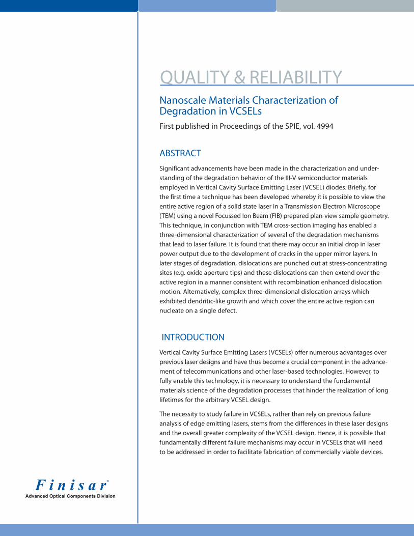
Figure 1. Schematic of the finished plan-view sample geometry.
In this work, a FEI FIB200 employing a 30keV gallium ion source.
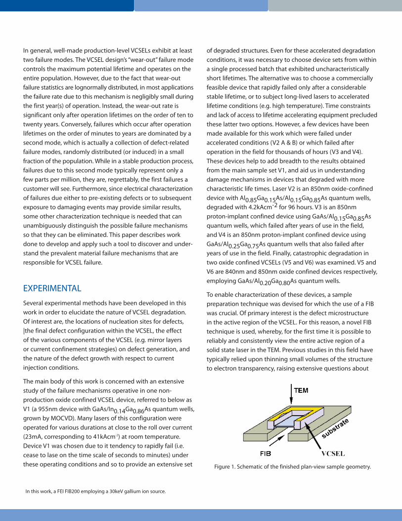
the statistical significance of such small sample regions, andthe conclusions drawn therefrom. Using the present technique,the active region is isolated with the FIB in a plan-viewconfiguration as depicted in Figure 1 and Figure 2. It shouldbe noted that a few mirror layers are left intact on either sideof the membrane in order to prevent damage to the activeregion. Furthermore, as is seen in some of the plan-view datapresented below, a slight unintentional angle between theGa+ beam and the heteroepitaxial planes of the VCSEL causesthe membrane surface to intersect several DBR layers as isshown in Figure 2. Plan-view samples manufactured underslight tilt will thus exhibit bands of contrast associated withthe intersection of different DBR layers with the membranesurface. The bands may be in the form of bars perpendicularto the beam direction, or if the membrane is slightly bent, theremay instead be non-uniform regions of contrast variation.
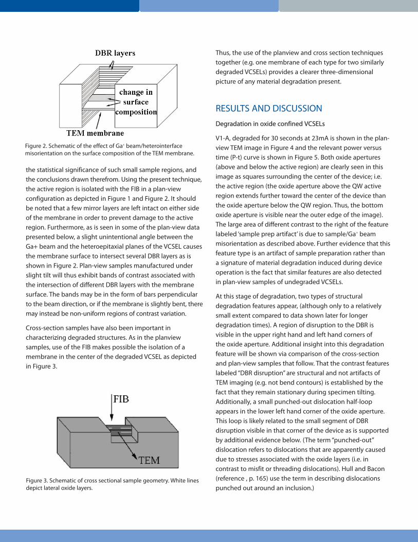
Cross-section samples have also been important incharacterizing degraded structures. As in the planviewsamples, use of the FIB makes possible the isolation of amembrane in the center of the degraded VCSEL as depictedin Figure 3.
Thus, the use of the planview and cross section techniquestogether (e.g. one membrane of each type for two similarlydegraded VCSELs) provides a clearer three-dimensionalpicture of any material degradation present.
RESULTS AND DISCUSSION
Degradation in oxide confined VCSELs
V1-A, degraded for 30 seconds at 23mA is shown in the plan-view TEM image in Figure 4 and the relevant power versustime (P-t) curve is shown in Figure 5. Both oxide apertures(above and below the active region) are clearly seen in thisimage as squares surrounding the center of the device; i.e. the active region (the oxide aperture above the QW activeregion extends further toward the center of the device thanthe oxide aperture below the QW region. Thus, the bottomoxide aperture is visible near the outer edge of the image).The large area of different contrast to the right of the featurelabeled ‘sample prep artifact’ is due to sample/Ga+ beammisorientation as described above. Further evidence that thisfeature type is an artifact of sample preparation rather than a signature of material degradation induced during deviceoperation is the fact that similar features are also detected in plan-view samples of undegraded VCSELs.
At this stage of degradation, two types of structuraldegradation features appear, (although only to a relativelysmall extent compared to data shown later for longerdegradation times). A region of disruption to the DBR isvisible in the upper right hand and left hand corners of the oxide aperture. Additional insight into this degradationfeature will be shown via comparison of the cross-section and plan-view samples that follow. That the contrast featureslabeled “DBR disruption” are structural and not artifacts ofTEM imaging (e.g. not bend contours) is established by thefact that they remain stationary during specimen tilting.Additionally, a small punched-out dislocation half-loopappears in the lower left hand corner of the oxide aperture.This loop is likely related to the small segment of DBRdisruption visible in that corner of the device as is supportedby additional evidence below. (The term “punched-out”dislocation refers to dislocations that are apparently causeddue to stresses associated with the oxide layers (i.e. incontrast to misfit or threading dislocations). Hull and Bacon(reference , p. 165) use the term in describing dislocationspunched out around an inclusion.)
Figure 2. Schematic of the effect of Ga+ beam/heterointerfacemisorientation on the surface composition of the TEM membrane.
Figure 3. Schematic of cross sectional sample geometry. White linesdepict lateral oxide layers.
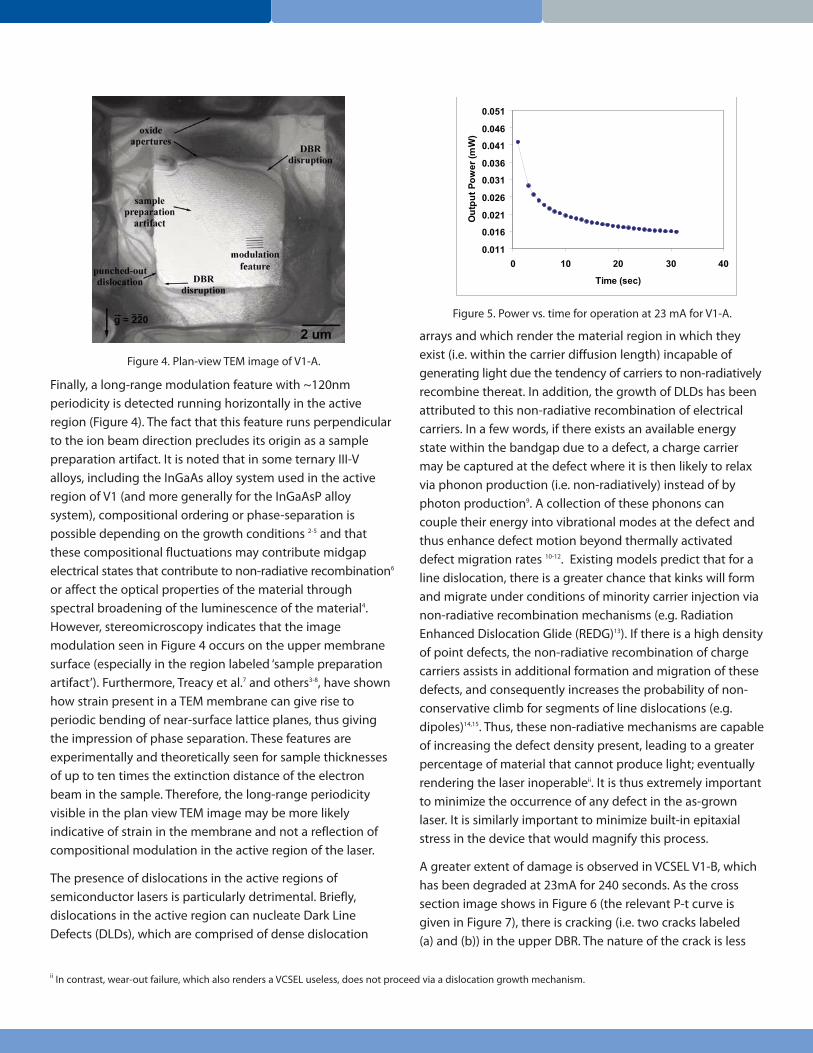
Finally, a long-range modulation feature with ~120nmperiodicity is detected running horizontally in the activeregion (Figure 4). The fact that this feature runs perpendicularto the ion beam direction precludes its origin as a samplepreparation artifact. It is noted that in some ternary III-Valloys, including the InGaAs alloy system used in the activeregion of V1 (and more generally for the InGaAsP alloysystem), compositional ordering or phase-separation ispossible depending on the growth conditions 2-5 and thatthese compositional fluctuations may contribute midgapelectrical states that contribute to non-radiative recombination6
or affect the optical properties of the material throughspectral broadening of the luminescence of the material4.However, stereomicroscopy indicates that the imagemodulation seen in Figure 4 occurs on the upper membranesurface (especially in the region labeled ‘sample preparationartifact’). Furthermore, Treacy et al.7 and others3-8, have shownhow strain present in a TEM membrane can give rise toperiodic bending of near-surface lattice planes, thus givingthe impression of phase separation. These features areexperimentally and theoretically seen for sample thicknessesof up to ten times the extinction distance of the electronbeam in the sample. Therefore, the long-range periodicityvisible in the plan view TEM image may be more likelyindicative of strain in the membrane and not a reflection ofcompositional modulation in the active region of the laser.
The presence of dislocations in the active regions ofsemiconductor lasers is particularly detrimental. Briefly,dislocations in the active region can nucleate Dark LineDefects (DLDs), which are comprised of dense dislocation
arrays and which render the material region in which theyexist (i.e. within the carrier diffusion length) incapable ofgenerating light due the tendency of carriers to non-radiativelyrecombine thereat. In addition, the growth of DLDs has beenattributed to this non-radiative recombination of electricalcarriers. In a few words, if there exists an available energystate within the bandgap due to a defect, a charge carriermay be captured at the defect where it is then likely to relaxvia phonon production (i.e. non-radiatively) instead of byphoton production9. A collection of these phonons cancouple their energy into vibrational modes at the defect andthus enhance defect motion beyond thermally activateddefect migration rates 10-12. Existing models predict that for aline dislocation, there is a greater chance that kinks will formand migrate under conditions of minority carrier injection vianon-radiative recombination mechanisms (e.g. RadiationEnhanced Dislocation Glide (REDG)13). If there is a high densityof point defects, the non-radiative recombination of chargecarriers assists in additional formation and migration of thesedefects, and consequently increases the probability of non-conservative climb for segments of line dislocations (e.g.dipoles)14,15. Thus, these non-radiative mechanisms are capableof increasing the defect density present, leading to a greaterpercentage of material that cannot produce light; eventuallyrendering the laser inoperableii. It is thus extremely importantto minimize the occurrence of any defect in the as-grownlaser. It is similarly important to minimize built-in epitaxialstress in the device that would magnify this process.
A greater extent of damage is observed in VCSEL V1-B, whichhas been degraded at 23mA for 240 seconds. As the crosssection image shows in Figure 6 (the relevant P-t curve isgiven in Figure 7), there is cracking (i.e. two cracks labeled (a) and (b)) in the upper DBR. The nature of the crack is less
Figure 4. Plan-view TEM image of V1-A.
0.011
0.016
0.021
0.026
0.031
0.036
0.041
0.046
0.051
0 10 20 30 40
Time (sec)
Out
put P
ower
(mW
)
Figure 5. Power vs. time for operation at 23 mA for V1-A.
ii In contrast, wear-out failure, which also renders a VCSEL useless, does not proceed via a dislocation growth mechanism.
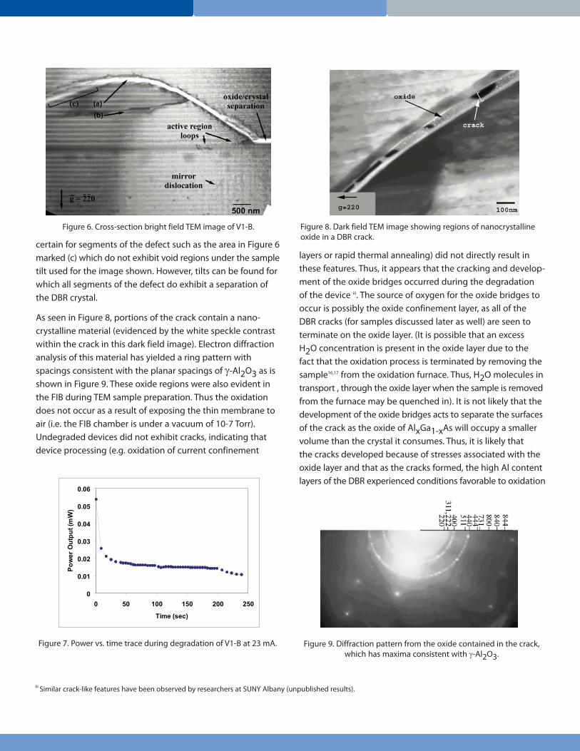
certain for segments of the defect such as the area in Figure 6marked (c) which do not exhibit void regions under the sampletilt used for the image shown. However, tilts can be found forwhich all segments of the defect do exhibit a separation ofthe DBR crystal.
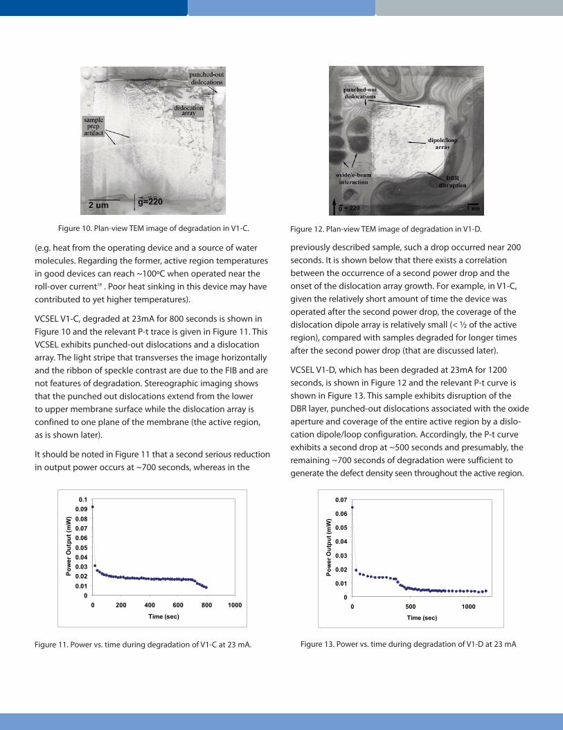
As seen in Figure 8, portions of the crack contain a nano-crystalline material (evidenced by the white speckle contrastwithin the crack in this dark field image). Electron diffractionanalysis of this material has yielded a ring pattern withspacings consistent with the planar spacings of γ-Al2O3 as isshown in Figure 9. These oxide regions were also evident inthe FIB during TEM sample preparation. Thus the oxidationdoes not occur as a result of exposing the thin membrane toair (i.e. the FIB chamber is under a vacuum of 10-7 Torr).Undegraded devices did not exhibit cracks, indicating thatdevice processing (e.g. oxidation of current confinement
layers or rapid thermal annealing) did not directly result inthese features. Thus, it appears that the cracking and develop-ment of the oxide bridges occurred during the degradation of the device iii. The source of oxygen for the oxide bridges tooccur is possibly the oxide confinement layer, as all of the DBR cracks (for samples discussed later as well) are seen toterminate on the oxide layer. (It is possible that an excess H2O concentration is present in the oxide layer due to thefact that the oxidation process is terminated by removing thesample16,17 from the oxidation furnace. Thus, H2O molecules intransport , through the oxide layer when the sample is removedfrom the furnace may be quenched in). It is not likely that thedevelopment of the oxide bridges acts to separate the surfacesof the crack as the oxide of AlxGa1-xAs will occupy a smallervolume than the crystal it consumes. Thus, it is likely that the cracks developed because of stresses associated with theoxide layer and that as the cracks formed, the high Al contentlayers of the DBR experienced conditions favorable to oxidation
0
0.01
0.02
0.03
0.04
0.05
0.06
0 50 100 150 200 250
Time (sec)
Pow
er O
utpu
t (m
W)
Figure 6. Cross-section bright field TEM image of V1-B.
Figure 7. Power vs. time trace during degradation of V1-B at 23 mA.
iii Similar crack-like features have been observed by researchers at SUNY Albany (unpublished results).
Figure 8. Dark field TEM image showing regions of nanocrystallineoxide in a DBR crack.
Figure 9. Diffraction pattern from the oxide contained in the crack,which has maxima consistent with γ-Al2O3.
(e.g. heat from the operating device and a source of watermolecules. Regarding the former, active region temperaturesin good devices can reach ~100ºC when operated near theroll-over current18 . Poor heat sinking in this device may havecontributed to yet higher temperatures).
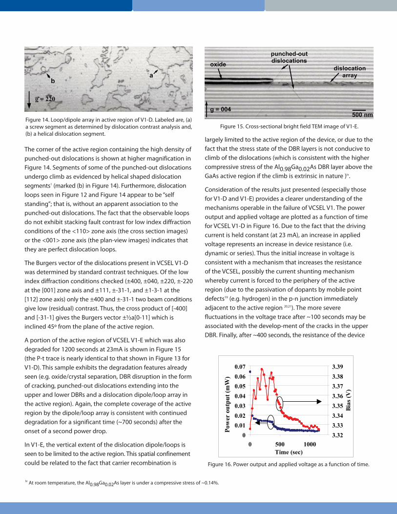
VCSEL V1-C, degraded at 23mA for 800 seconds is shown inFigure 10 and the relevant P-t trace is given in Figure 11. ThisVCSEL exhibits punched-out dislocations and a dislocationarray. The light stripe that transverses the image horizontallyand the ribbon of speckle contrast are due to the FIB and arenot features of degradation. Stereographic imaging showsthat the punched out dislocations extend from the lower to upper membrane surface while the dislocation array isconfined to one plane of the membrane (the active region, as is shown later).
It should be noted in Figure 11 that a second serious reductionin output power occurs at ~700 seconds, whereas in the
previously described sample, such a drop occurred near 200seconds. It is shown below that there exists a correlationbetween the occurrence of a second power drop and theonset of the dislocation array growth. For example, in V1-C,given the relatively short amount of time the device wasoperated after the second power drop, the coverage of thedislocation dipole array is relatively small (< ½ of the activeregion), compared with samples degraded for longer timesafter the second power drop (that are discussed later).
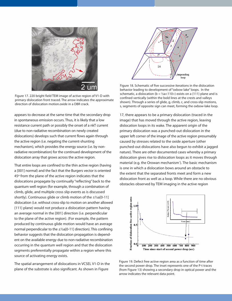
VCSEL V1-D, which has been degraded at 23mA for 1200seconds, is shown in Figure 12 and the relevant P-t curve isshown in Figure 13. This sample exhibits disruption of theDBR layer, punched-out dislocations associated with the oxideaperture and coverage of the entire active region by a dislo-cation dipole/loop configuration. Accordingly, the P-t curveexhibits a second drop at ~500 seconds and presumably, theremaining ~700 seconds of degradation were sufficient togenerate the defect density seen throughout the active region.
00.010.020.030.040.050.060.070.080.09
0.1
0 200 400 600 800 1000
Time (sec)
Pow
er O
utpu
t (m
W)
Figure 10. Plan-view TEM image of degradation in V1-C.
Figure 11. Power vs. time during degradation of V1-C at 23 mA.
Figure 12. Plan-view TEM image of degradation in V1-D.
0
0.01
0.02
0.03
0.04
0.05
0.06
0.07
0 500 1000
Time (sec)
Pow
er O
utpu
t (m
W)
Figure 13. Power vs. time during degradation of V1-D at 23 mA
The corner of the active region containing the high density ofpunched-out dislocations is shown at higher magnification inFigure 14. Segments of some of the punched-out dislocationsundergo climb as evidenced by helical shaped dislocationsegments1 (marked (b) in Figure 14). Furthermore, dislocationloops seen in Figure 12 and Figure 14 appear to be “selfstanding”; that is, without an apparent association to thepunched-out dislocations. The fact that the observable loopsdo not exhibit stacking fault contrast for low index diffractionconditions of the <110> zone axis (the cross section images)or the <001> zone axis (the plan-view images) indicates thatthey are perfect dislocation loops.
The Burgers vector of the dislocations present in VCSEL V1-Dwas determined by standard contrast techniques. Of the lowindex diffraction conditions checked (±400, ±040, ±220, ±-220at the [001] zone axis and ±111, ±-31-1, and ±1-3-1 at the[112] zone axis) only the ±400 and ±-31-1 two beam conditionsgive low (residual) contrast. Thus, the cross product of [-400]and [-31-1] gives the Burgers vector ±½a[0-11] which isinclined 45º from the plane of the active region.
A portion of the active region of VCSEL V1-E which was alsodegraded for 1200 seconds at 23mA is shown in Figure 15(the P-t trace is nearly identical to that shown in Figure 13 forV1-D). This sample exhibits the degradation features alreadyseen (e.g. oxide/crystal separation, DBR disruption in the formof cracking, punched-out dislocations extending into theupper and lower DBRs and a dislocation dipole/loop array inthe active region). Again, the complete coverage of the activeregion by the dipole/loop array is consistent with continueddegradation for a significant time (~700 seconds) after theonset of a second power drop.
In V1-E, the vertical extent of the dislocation dipole/loops isseen to be limited to the active region. This spatial confinementcould be related to the fact that carrier recombination is
largely limited to the active region of the device, or due to thefact that the stress state of the DBR layers is not conducive toclimb of the dislocations (which is consistent with the highercompressive stress of the Al0.98Ga0.02As DBR layer above theGaAs active region if the climb is extrinsic in nature )iv.
Consideration of the results just presented (especially thosefor V1-D and V1-E) provides a clearer understanding of themechanisms operable in the failure of VCSEL V1. The poweroutput and applied voltage are plotted as a function of timefor VCSEL V1-D in Figure 16. Due to the fact that the drivingcurrent is held constant (at 23 mA), an increase in appliedvoltage represents an increase in device resistance (i.e.dynamic or series). Thus the initial increase in voltage isconsistent with a mechanism that increases the resistance of the VCSEL, possibly the current shunting mechanismwhereby current is forced to the periphery of the activeregion (due to the passivation of dopants by mobile pointdefects19 (e.g. hydrogen) in the p-n junction immediatelyadjacent to the active region 20,21). The more severefluctuations in the voltage trace after ~100 seconds may beassociated with the develop-ment of the cracks in the upperDBR. Finally, after ~400 seconds, the resistance of the device
Figure 14. Loop/dipole array in active region of V1-D. Labeled are, (a)a screw segment as determined by dislocation contrast analysis and,(b) a helical dislocation segment.
Figure 15. Cross-sectional bright field TEM image of V1-E.
iv At room temperature, the Al0.98Ga0.02As layer is under a compressive stress of ~0.14%.
00.010.020.030.040.050.060.07
0 500 1000Time (sec)
Pow
er o
utpu
t (m
W)
3.323.333.343.353.363.373.383.39
Bias
(V)
Figure 16. Power output and applied voltage as a function of time.
appears to decrease at the same time that the secondary dropin spontaneous emission occurs. Thus, it is likely that a lowresistance current path or possibly the onset of a nkT current(due to non-radiative recombination on newly createddislocations) develops such that current flows again throughthe active region (i.e. negating the current-shuntingmechanism), which provides the energy source (i.e. by non-radiative recombination) for the continued development of thedislocation array that grows across the active region.
That entire loops are confined to the thin active region (havinga [001] normal) and the fact that the Burgers vector is oriented45º from the plane of the active region indicates that thedislocations propagate by continually “reflecting” back to thequantum well region (for example, through a combination ofclimb, glide, and multiple cross slip events as is discussedshortly). Continuous glide or climb motion of the ±½a[0-11]dislocation (i.e. without cross-slip to motion on another allowed111 plane) would not produce a dislocation pattern havingan average normal in the [001] direction (i.e. perpendicular to the plane of the active region). (For example, the patternproduced by continuous glide motion would have an averagenormal perpendicular to the ±½a[0-11] direction). This confiningbehavior suggests that the dislocation propagation is depend-ent on the available energy due to non-radiative recombinationoccurring in the quantum well region and that the dislocationsegments preferentially propagate within a region where thissource of activating energy exists.
The spatial arrangement of dislocations in VCSEL V1-D in theplane of the substrate is also significant. As shown in Figure
17, there appears to be a primary dislocation (traced in theimage) that has moved through the active region, leavingdislocation loops in its wake. The apparent origin of theprimary dislocation was a punched-out dislocation in theupper left corner of the image of the active region presumablycaused by stresses related to the oxide aperture (otherpunched-out dislocations have also begun to exhibit a jaggednature). There are other documented cases whereby a primarydislocation gives rise to dislocation loops as it moves throughmaterial (e.g. the Orowan mechanism1). The basic mechanismis one in which a dislocation bows around an obstacle to the extent that the separated fronts meet and form a newdislocation front as well as a loop. While there are no obviousobstacles observed by TEM imaging in the active region
Figure 17. 220 bright field TEM image of active region of V1-D withprimary dislocation front traced. The arrow indicates the approximatedirection of dislocation motion.oxide in a DBR crack.
Figure 18. Schematic of five successive iterations in the dislocationbehavior leading to development of “oxbow lake” loops. In theschematic, a dislocation (b = ½a<110>) exists on a 111 plane and isconfined vertically (within the bold lines at the crests and valleysshown). Through a series of glide, g, climb, c, and cross-slip motions,s, segments of opposite sign can meet, forming the oxbow-lake loop.
Figure 19. Defect free active region area as a function of time afterthe second power drop. The inset represents one of the P-t traces(from Figure 13) showing a secondary drop in optical power and thearrow indicates the relevant data point.
of V1-D, it appears that as fingers of the primary dislocationdeveloped, some of them met, forming a new dislocationfront and leaving “oxbow-lake” loops behind. Thus, a model is proposed, as explained below, whereby the only obstaclesleading to the development of the oxbow-lake loops are theheteroepitaxial interfaces bounding (and those possiblywithin) the active region of the device.
As was seen previously, the dislocations are generally containedwithin the inner edges of the DBRs. Thus the upper and lowerbounds of the active region, acting as obstacles to the dislo-cation, may lead to the development of the oxbow-lake dislo-cations. A possible scenario by which this might occur isdepicted in Figure 18. The schematic depicts five successivesnapshots of a growing dislocation loop, although thisproposed model works equally well for a long dislocationsegment passing through the region depicted. The terrainshown is a random set of 111 planes, which are the sets ofplanes on which dislocations in zinc-blende semiconductorsglide. In the model, the dislocation is prohibited from movingabove or below the region depicted (the boundaries of whichare marked by bold lines on the crests and in the valleys)similar to the manner in which the dislocations underdiscussion are confined to the active region. As the loopexpands, screw portions of the loop may cross slip onto other111 planes containing the ½a<110> type Burgers vector (i.e.similar to the model in which multiple cross-slip occurs underconditions of recombination assisted dislocation motion asproposed by Matsui et. al.22). Upon reaching the upper orlower boundary of the region, edge or mixed charactersegments may be induced to switch from glide motion toclimb motion (on a 111 plane not containing the Burgersvector) or vice versa. Thus, as depicted, a series of theseactions may produce a dislocation front with a jagged nature,
some fingers of which can meet, annihilate and form oxbow-lake dislocation loops. While the residual stress state presentin the VCSEL is initially complex and further complicated bythe introduction of the dislocation array into the activeregion, it must be assumed in applying this model to VCSELV1-D that the average stress state is one which favors theoccurrence of repeated cross-slip and glide-to-climborientations such that the net dislocation motion is in thedirection shown in Figure 17.
Finally, Figure 19 shows a plot of the fraction of defect freeactive region of the V1 samples as a function of time after thesecondary power drop (e.g. as occurred at ~400 seconds forV1-D as shown in Figure 13). Here, the defect free activeregion is the area of the active region through which nodislocations have traversed. In areas where dislocations doexist the dislocation spacing is typically less than 1um(approximately the minority carrier diffusion length for III-Vmaterials23-26). Thus, luminescence from these areas will besignificantly decreased as carriers migrate to and non-radiatively recombine at the dislocations. This graph lendssupport to the argument that the secondary drop in powerindicates the onset of dislocation propagation throughout the active region. Specifically, the two data points with adislocation free active region area of ~37µm2 are fromsamples V1-B and V1-C operated for a total time of 240seconds and 800 seconds respectively, thus illustrating amuch stronger correlation between the dislocation free activeregion and the time after the second power drop than there is between the dislocation free active region and the totaloperating time. As further evidence of this relationship, for V1
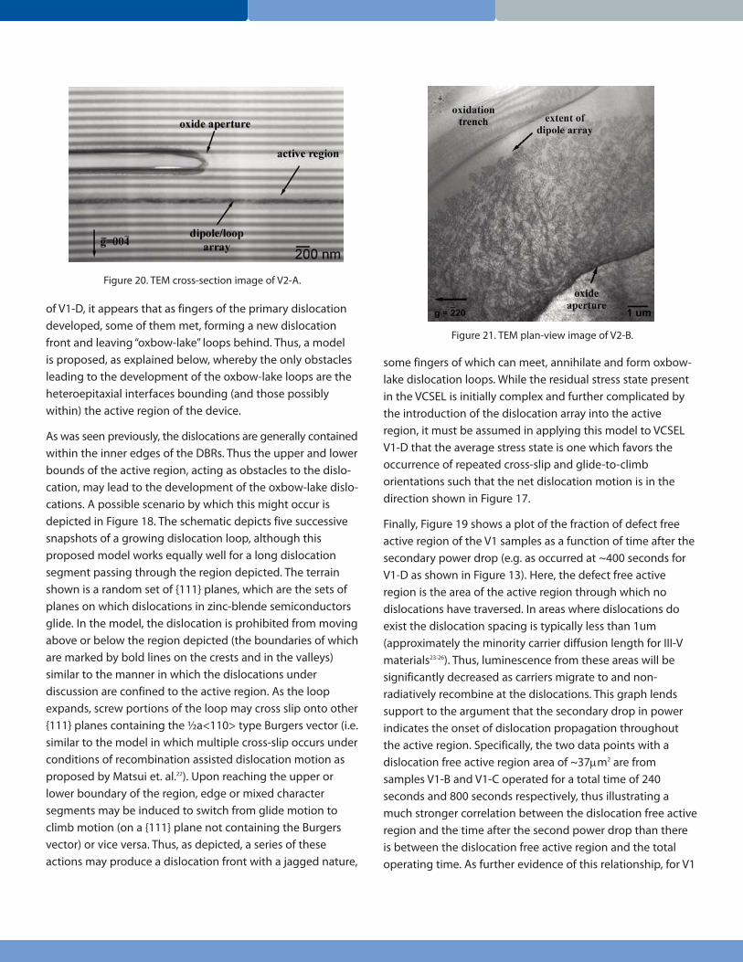
Figure 20. TEM cross-section image of V2-A.
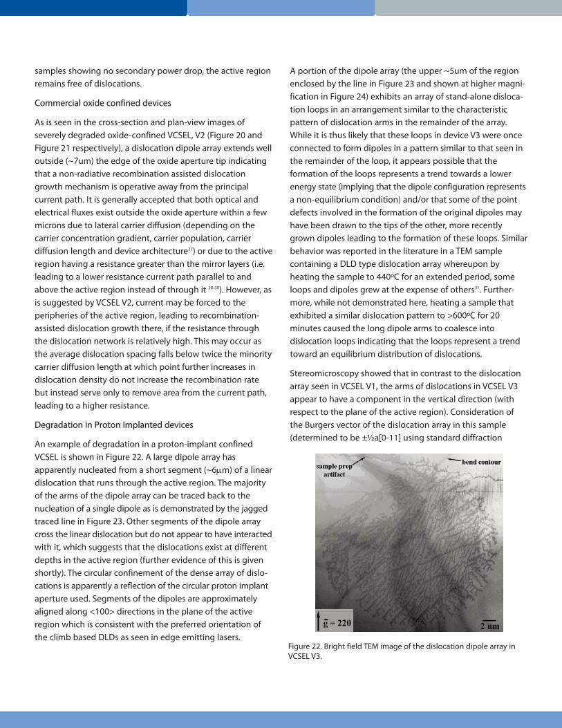
Figure 21. TEM plan-view image of V2-B.
samples showing no secondary power drop, the active regionremains free of dislocations.
Commercial oxide confined devices
As is seen in the cross-section and plan-view images ofseverely degraded oxide-confined VCSEL, V2 (Figure 20 andFigure 21 respectively), a dislocation dipole array extends welloutside (~7um) the edge of the oxide aperture tip indicatingthat a non-radiative recombination assisted dislocationgrowth mechanism is operative away from the principalcurrent path. It is generally accepted that both optical andelectrical fluxes exist outside the oxide aperture within a fewmicrons due to lateral carrier diffusion (depending on thecarrier concentration gradient, carrier population, carrierdiffusion length and device architecture27) or due to the activeregion having a resistance greater than the mirror layers (i.e.leading to a lower resistance current path parallel to andabove the active region instead of through it 28-30). However, asis suggested by VCSEL V2, current may be forced to theperipheries of the active region, leading to recombination-assisted dislocation growth there, if the resistance throughthe dislocation network is relatively high. This may occur asthe average dislocation spacing falls below twice the minoritycarrier diffusion length at which point further increases indislocation density do not increase the recombination ratebut instead serve only to remove area from the current path,leading to a higher resistance.
Degradation in Proton Implanted devices
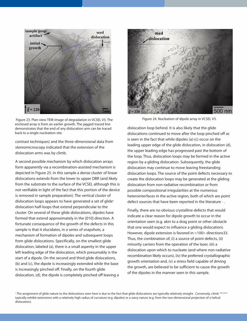
An example of degradation in a proton-implant confinedVCSEL is shown in Figure 22. A large dipole array hasapparently nucleated from a short segment (~6µm) of a lineardislocation that runs through the active region. The majorityof the arms of the dipole array can be traced back to thenucleation of a single dipole as is demonstrated by the jaggedtraced line in Figure 23. Other segments of the dipole arraycross the linear dislocation but do not appear to have interactedwith it, which suggests that the dislocations exist at differentdepths in the active region (further evidence of this is givenshortly). The circular confinement of the dense array of dislo-cations is apparently a reflection of the circular proton implantaperture used. Segments of the dipoles are approximatelyaligned along <100> directions in the plane of the activeregion which is consistent with the preferred orientation ofthe climb based DLDs as seen in edge emitting lasers.
A portion of the dipole array (the upper ~5um of the regionenclosed by the line in Figure 23 and shown at higher magni-fication in Figure 24) exhibits an array of stand-alone disloca-tion loops in an arrangement similar to the characteristicpattern of dislocation arms in the remainder of the array.While it is thus likely that these loops in device V3 were onceconnected to form dipoles in a pattern similar to that seen inthe remainder of the loop, it appears possible that theformation of the loops represents a trend towards a lowerenergy state (implying that the dipole configuration representsa non-equilibrium condition) and/or that some of the pointdefects involved in the formation of the original dipoles mayhave been drawn to the tips of the other, more recentlygrown dipoles leading to the formation of these loops. Similarbehavior was reported in the literature in a TEM samplecontaining a DLD type dislocation array whereupon byheating the sample to 440ºC for an extended period, someloops and dipoles grew at the expense of others31. Further-more, while not demonstrated here, heating a sample thatexhibited a similar dislocation pattern to >600ºC for 20minutes caused the long dipole arms to coalesce intodislocation loops indicating that the loops represent a trendtoward an equilibrium distribution of dislocations.
Stereomicroscopy showed that in contrast to the dislocationarray seen in VCSEL V1, the arms of dislocations in VCSEL V3appear to have a component in the vertical direction (withrespect to the plane of the active region). Consideration ofthe Burgers vector of the dislocation array in this sample(determined to be ±½a[0-11] using standard diffraction
Figure 22. Bright field TEM image of the dislocation dipole array inVCSEL V3.
contrast techniques) and the three-dimensional data fromstereomicroscopy indicated that the extension of thedislocation arms was by climb.
A second possible mechanism by which dislocation arraysform apparently via a recombination-assisted mechanism isdepicted in Figure 25. In this sample a dense cluster of lineardislocations extends from the lower to upper DBR (and likelyfrom the substrate to the surface of the VCSEL although this isnot verifiable in light of the fact that this portion of the deviceis removed in sample preparation). The vertical cluster ofdislocation loops appears to have generated a set of glidev
dislocation half-loops that extend perpendicular to thecluster. On several of these glide dislocations, dipoles haveformed that extend approximately in the [010] direction. Afortunate consequence of the growth of the defects in thissample is that it elucidates, in a series of snapshots, amechanism of formation of dipoles and subsequent loopsfrom glide dislocations. Specifically, on the smallest glidedislocation, labeled (a), there is a small asperity in the upperleft leading edge of the dislocation, which presumably is thestart of a dipole. On the second and third glide dislocations,(b) and (c), the dipole is increasingly extended while the baseis increasingly pinched off. Finally, on the fourth glidedislocation, (d), the dipole is completely pinched off leaving a
dislocation loop behind. It is also likely that the glidedislocations continued to move after the loop pinched off asis seen in the fact that while dipoles (a)-(c) occur on theleading upper edge of the glide dislocation, in dislocation (d),the upper leading edge has progressed past the bottom ofthe loop. Thus, dislocation loops may be formed in the activeregion by a gliding dislocation. Subsequently, the glidedislocation may continue to move leaving freestandingdislocation loops. The source of the point defects necessary tocreate the dislocation loops may be generated at the glidingdislocation from non-radiative recombination or frompossible compositional irregularities at the numerousheterointerfaces in the active region, both of which are pointdefect sources that have been reported in the literature - .
Finally, there are no obvious crystalline defects that wouldindicate a clear reason for dipole growth to occur in theorientation seen (e.g. akin to a drag point or other obstaclethat one would expect to influence a gliding dislocation).However, dipole extension is favored in <100> directions33.Thus, the combination of, (i) a source of point defects, (ii)minority carriers from the operation of the laser, (iii) adislocation upon which to nucleate (and where non-radiativerecombination likely occurs), (iv) the preferred crystallographicgrowth orientation and, (v) a stress field capable of drivingthe growth, are believed to be sufficient to cause the growthof the dipoles in the manner seen in this sample.
Figure 23. Plan-view TEM image of degradation in VCSEL V3. Theenclosed array is from an earlier growth. The jagged traced linedemonstrates that the end of any dislocation arm can be tracedback to a single nucleation site.
Figure 24. Nucleation of dipole array in VCSEL V3.
v The assignment of glide nature to the dislocations seen here is due to the fact that glide dislocations are typically relatively straight. Conversely, climb dislocations
typically exhibit extensions with a relatively high radius of curvature (e.g. dipoles) or a wavy nature (e.g. from the two-dimensional projection of a helicaldislocation).
Catastrophic failure
Devices subjected to unintentional high current pulses such that output powers reach 106W/cm2 typically degradecatastrophically due to the extreme optical density and/orheating. Alternatively, if a device is operated under constantpower conditions (i.e. such that current varies to keep theoutput power constant), current densities near the end of theVCSEL lifetime increase sharply as the efficiency decreases,and the VCSEL can fail due to electrical overstress38,39.
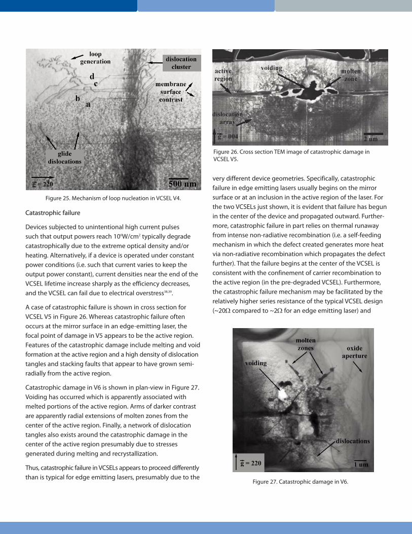
A case of catastrophic failure is shown in cross section forVCSEL V5 in Figure 26. Whereas catastrophic failure oftenoccurs at the mirror surface in an edge-emitting laser, thefocal point of damage in V5 appears to be the active region.Features of the catastrophic damage include melting and voidformation at the active region and a high density of dislocationtangles and stacking faults that appear to have grown semi-radially from the active region.
Catastrophic damage in V6 is shown in plan-view in Figure 27.Voiding has occurred which is apparently associated withmelted portions of the active region. Arms of darker contrastare apparently radial extensions of molten zones from thecenter of the active region. Finally, a network of dislocationtangles also exists around the catastrophic damage in thecenter of the active region presumably due to stressesgenerated during melting and recrystallization.
Thus, catastrophic failure in VCSELs appears to proceed differentlythan is typical for edge emitting lasers, presumably due to the
very different device geometries. Specifically, catastrophicfailure in edge emitting lasers usually begins on the mirrorsurface or at an inclusion in the active region of the laser. Forthe two VCSELs just shown, it is evident that failure has begunin the center of the device and propagated outward. Further-more, catastrophic failure in part relies on thermal runawayfrom intense non-radiative recombination (i.e. a self-feedingmechanism in which the defect created generates more heatvia non-radiative recombination which propagates the defectfurther). That the failure begins at the center of the VCSEL isconsistent with the confinement of carrier recombination tothe active region (in the pre-degraded VCSEL). Furthermore,the catastrophic failure mechanism may be facilitated by therelatively higher series resistance of the typical VCSEL design(~20Ω compared to ~2Ω for an edge emitting laser) and
Figure 25. Mechanism of loop nucleation in VCSEL V4.
Figure 26. Cross section TEM image of catastrophic damage in VCSEL V5.
Figure 27. Catastrophic damage in V6.
thus greater degree of joule heating. Lastly, the fact that theoptical and electrical field intensities are greatest at the centerof the device (due to the high reflectivity of the DBR mirrorsand to current confinement techniques respectively) arefurther reasons for catastrophic failure to begin at the centerof the device. Therefore, following the models given forcatastrophic failure in edge emitting lasers, the catastrophicfailure of these VCSELs likely proceeds as follows. A preexistingdefect or a defect such as a dislocation array occurs in theactive region. Intense non-radiative recombination (due togreater than normal driving conditions such as a current spikeor due to a rise in the drive current as the laser degradesunder constant power operation) occurs at this defect leadingto the melting of the nearby material. Intense non-radiativerecombination continues on the molten material furtherpropagating the molten arm. A tangle of dislocations is formedto compensate for the stresses involved in the melting andsolidification of these arms.
CONCLUSIONS
Several new and important results have been discussed in thispaper. For the first time a technique has been developedwhereby it is possible to view the entire active region of a solidstate laser in a TEM and thereby conclusively identify the degra-dation mechanisms that lead to laser failure. These techniqueshave been systematically applied to the characterization of asingle, rapidly failing VCSEL device structure thus showing theevolution of material failure in the device and ultimately linkingthe material failure to the output characteristics of the device.Additional examples of degraded VCSELs, drawn from a widerset of failure conditions, were examined to give breadth to ourunderstanding of VCSEL failure mechanisms.
In non-production VCSEL V1, the degradation proceeds asfollows. There is an initial drop in laser output due to the develop-ment of cracks in the upper DBR layers (leading to a loss ofthe resonance cavity) and also, possibly due to a mechanismsuch as current shunting. Although this latter mechanism isnot readily detected by TEM, it appears to be a likely cause ofdegradation in the absence of damage to the DBR or a dislo-cation network in the active region. The force driving crackpropagation is not fully understood at this time. However, theoxide layers do seem to be involved in the crack formation (allof the observed cracks ended on the oxide layers).
The damage to the DBR is typically connected with separationof the upper DBR from the oxide layers and in some instancesextends over the entire active region. In some cases, dislocationsare punched out near the oxide aperture presumably due tostresses associated with damage to the DBR layers. That thesedislocations are a result of the damage to the DBR layers (asopposed to the cause of it) is seen by the fact that several ofthe V1 devices (not shown in this paper) exhibited crackingbut no dislocations while the opposite scenario (i.e. disloca-tions without cracking) was not observed. Some of thesepunched-out dislocations then extend over the active region,presumably by a combined process of climb and glide thatkeeps them largely confined to the active region. The controllingparameter is likely non-radiative recombination in the activeregion that supplies energy for the evolution of the dislocationarray. The Burgers vector of the dislocations in VCSEL V1 is ½a[0-11], which is inclined 45º to the plane of the lasersubstrate and the type of which is consistent with the Burgersvector for dislocations in III-V semiconductors. Freestandingdislocation loops which are left in the active region areexplained by a process in which segments of the jaggeddislocation front meet and form a new front leaving a loopbehind. The jagged nature of the dislocation front can beexplained by a combination of cross-slip and fluctuationbetween climb and glide due to confinement of thedislocation motion to the active region. Furthermore, it hasbeen shown how the beginning and extent of active regioncoverage by the dislocation array can be determined by theonset and duration of time after a secondary drop in thepower versus time curve.
Two additional mechanisms for the formation of stand-alonedislocation loops seen in the active regions of failed lasers arealso described. In the first, the individual extended arms of adislocation array pinch off to form loops. In the second, agliding dislocation grows a dislocation dipole that eventuallypinches off to form a free standing loop. The loops formedfrom these two mechanisms, as well as those seen in VCSELV1 do not exhibit stacking faults as evidenced by the lack ofstacking fault image contrast for all of the several diffractionconditions employed.
Some of the VCSELs studied (especially V3 and V4)demonstrate the role that preexisting defects play in laserfailure. Specifically, in these devices, complex dislocationarrays were shown to nucleate on a single grown-in defect.
Thus, while the dislocation arrays lead to the loss of laseroutput, the initial preexisting defect was ultimatelyresponsible for the laser failure.
Finally, the study of catastrophically failed VCSELs shown inthis paper demonstrates that several of the degradationmechanisms that occur during the catastrophic failure ofedge emitting lasers are also operative in VCSELs. Namely,laser material is melted and resolidified causing the formationof a tangle of dislocations. However, catastrophic failure inVCSELs is seen to originate at the active region in the centerof the device while it was reported to occur on mirror faces inedge emitting lasers. Presumably the cause for this differenceis the carrier recombination that occurs at the active region inthe center of the VCSEL.
ACKNOWLEDGEMENTS
This work has been supported by Sandia National Laboratoryand by the National Science Foundation, Division of MaterialsResearch, under grant numbers 9612283 and 0080630.
REFERENCES1 D. Hull, and D.J. Bacon, Introduction to Dislocations, 3rd
ed., Butterworth Heinemann, UK, 1984.
2 G. Stringfellow, “Miscibility gaps in quaternary III/V alloys”,J. Crystal Growth, 58, 194-202, 1982.
3 T.L. Mcdevitt, S. Mahajan, D.E. Laughlin, W.A. Bonner andV.G. Keramidas, “Two-dimensional phase separation inInxGa1-xAsyP1-y epitaxial layers”, Phys. Rev. B, 45(12),6614-6622, 1992.
4 D. Gonzalez, G. Aragon, D. Araujo, M.J. de Castro, and R.Garcia, “Growth rate and critical temperatures to avoid themodulation of composition of InGaAs epitaxial layers”,Appl. Phys. Lett., 74(18), 2649-2651, 1999.
5 D. Gonzalez, G. Aragon, D. Araujo, and R. Garcia, “Controlof phase modulation in InGaAs epilayers”, Appl. Phys. Lett.,76(22), 3236-3238, 2000.
6 P. Ernst, C. Geng, F. Scholz, and H. Schweizer, “Ordering inGaInP2 studied by optical spectroscopy”, Phys. Stat. Sol.(B), 193, 213-228, 1996.
7 M. Treacy, J.M. Gibson, and A. Howie, “On elastic relaxationand long wavelength microstructures in spinodallydecomposed InxGa1-xAsyP1-y epitaxial layers”, Phil. Mag.A, 51(3), 389-417, 1985.
8 S. Mahajan, M. Shahid, and D. Laughlin, “Current status ofatomic ordering and phase separation in ternary andquaternary III-V compound semiconductors”, Microscopyof Semiconducting Materials, Inst. Phys. Conf. Ser. No. 100sect. 3, 143-153, IOP Publishing Ltd. 1989.
9 V. Narayanamurti, R.A. Logan, and M.A. Chin, “Directobservation of phonons generated during nonradiativecapture in GaAs p-n junctions”, Phys. Rev. Lett., 40 63-66,1978.
10 R.D. Gold and L.R. Weisberg, “Permanent degradation ofGaAs tunnel diodes”, Solid State Electron, 7, 811-821, 1964.
11 D.V. Lang and L.C. Kimerling, “Observation ofrecombination-enhanced defect reactions insemiconductors”, Phys. Rev. Lett., 33(8), 489-492, 1974.
12 D.V. Lang and C.H. Henry, “Nonradiative recombination atdeep levels in GaAs and GaP by Lattice-RelaxationMultiphonon Emission”, Phys. Rev. Lett., 35(22) 1525-1528,1975.
13 P. Haasen, “Kink formation and migration as dependent onthe Fermi level”, J. De Physique, 40(C6) 111-116, 1979.
14 L.C. Kimerling, P.Petroff, and H.J. Leamy, “Injection-stimulated dislocation motion in semiconductors”, Appl.Phys. Lett., 28(6), 297-300, 1976.
15 P. Petroff and R.L. Hartman, “Defect structure introducedduring operation of heterojunction GaAs lasers”, Appl.Phys. Lett., 23(8), 469-471, 1973.
16 C.H. Ashby, M.M. bridges, A.A. Allerman, B.E. Hammons,H.Q Hou, “Origin of the time dependence of wet oxidationof AlGaAs”, Appl. Phys. Lett,. 75(1), 73-75, 1999.
17 S. Guha, F. Agahi, B. Pezeshki, J. A. Kish, D.W. Kisker, andN.A. Bojarczuk, “Microstructure of AlGaAs-oxideheterolayers formed by wet oxidation”, Appl. Phys. Lett.,68(7), 906-908, 1996.
18 C. Wilmsen, H. Temkin, and L.A. Coldren, Vertical-CavitySurface-Emitting Lasers, Cambridge University Press,Cambridge, UK, 1999.

19 R.B. Martins, O. Henoc, B. Akamatsu, and J.F. Palmier, “Amodel for the degradation of Ga(Al)As single-quantum-well lasers”, J. Appl. Phys., 70(2), 554-561, 1991.
20 R.W. Herrick, Degradation in Vertical Cavity Lasers, anElectrical Engineering Ph.D. Thesis, University of Californiaat Santa Barbara, 1997.
21 R.W. Herrick, and P.M. Petroff, “Gradual degradation in 850-nm vertical-cavity surface-emitting lasers”, IEEE J.Quantum Electronics, 34(10), 1963-1969, 1998.
22 J. Matsui, K. Ishida, and Y. Nannichi, “Rapid degradation indouble-heterostructure lasers. I. Proposal of a new modelfor the directional growth of dislocation networks”, Jap. JAppl. Phys., 14(10), 1555-1560, 1975.
23 P. Berger, N. Chand, and N. Dutta, “An AlGaAs double-heterojunction bipolar transistor grown by molecular-beam epitaxy”, Appl. Phys. Lett., 59(9), 1099-1101, 1991.
24 G. Grummt, G. Oelgart, and N. Puhlmann, “Transportlength variation due to dopant gradients in AlGaAs”,Semiconductor Science & Technology, 8(7), 1191-1195,1993.
25 D. Araujo, G. Oelgart, J. Ganiere, and F. Reinhart,“Comparison of the lateral carrier transport between aGaAs single quantum well and the AlGaAs barrier duringcathodoluminescence excitation”, J. Appl. Phys., 76(1), 342-346, 1994.
26 H. Zarem, J. Lebens, K. Nordstrom, P. Sercel, S. Sanders, L.Eng, A. Yariv, and K. Vahala, “Effect of Al mole fraction oncarrier diffusion lengths and lifetimes in AlxGA1-xs”, Appl.Phys. Lett., 55(25), 2622-2624, 1989.
27 W. Tsang, “The effects of lateral current spreading, carrierout-diffusion, and optical mode losses on the thresholdcurrent density of GaAs-AlxGa1-xAs stripe-geometry DHlasers”, J. Appl. Phys., 49(3), 1031-1044, 1978.
28 Personal communication with Kent Choquette, Universityof Illinois, Urbana Champaign.
29 B. Thibeault, E. Hegblom, Y. Akulova, J. Ko, R. Naone, L.Coldren, and P. Floyd, “Electrical and optical losses indielectrically apertured vertical cavity lasers”, VerticalCavity Surface Emitting Lasers, 3003, 86-99, 1997.
30 W. Joyce, “Current-crowded carrier confinement in double-heterostructure lasers”, J. Appl. Phys., 51(5), 2394-2401,1980.
©2007 Finisar Corporation. All rights reserved. Finisar is a registered trademark of Finisar Corporation. Features and specifications are subject to change without notice. 1/07
Phone:1-866-MY-VCSEL USA (toll free) 1-972-792-1800 USA (Direct dial) 44 (0) 174 336 5533 Europe 886-935-409898 China & Taiwan81-90-4437-1130 Japan82-11-220-6153 Asia Pacific & Korea
ADVANCED OPTICAL COMPONENTSFinisar’s ADVANCED OPTICAL COMPONENTS division wasformed through strategic acquisition of key optical compon-ent suppliers. The company has led the industry in highvolume Vertical Cavity Surface Emitting Laser (VCSEL) andassociated detector technology since 1996. VCSELs havebecome the primary laser source for optical data communi-cation, and are rapidly expanding into a wide variety of sensorapplications. VCSELs’ superior reliability, low drive current,high coupled power, narrow and circularly symmetric beamand versatile packaging options (including arrays) are enablingsolutions not possible with other optical technologies.ADVANCED OPTICAL COMPONENTS is also a key supplier ofFabrey-Perot (FP) and Distributed Feedback (DFB) Lasers, andOptical Isolators (OI) for use in single mode fiber data andtelecommunications networks
LOCATIONAllen, TX - Business unit headquarters, VCSEL wafergrowth, wafer fabrication and TO package assembly.
Fremont, CA – Wafer growth and fabrication of 1310 to1550nm FP and DFB lasers.
Shanghai, PRC – Optical passives assembly, includingoptical isolators and splitters.
SALES AND SERVICEFinisar’s ADVANCED OPTICAL COMPONENTS division serves itscustomers through a worldwide network of sales offices anddistributors. For application assistance, current specifications,pricing or name of the nearest Authorized Distributor, contacta nearby sales office or call the number listed below.
AOC CAPABILITIESADVANCED OPTICAL COMPONENTS’ advanced capabilitiesinclude:
1, 2, 4, 8, and 10Gbps serial VCSEL solutions
1, 2, 4, 8, and 10Gbps serial SW DETECTOR solutions
VCSEL and detector arrays
1, 2, 4, 8, and 10Gbps FP and DFB solutions at 1310 and1550nm
1, 2, 4, 8, and 10Gbps serial LW DETECTOR solutions
Optical Isolators from 1260 to 1600nm range
Laser packaging in TO46, TO56, and Opticalsubassemblies with SC, LC, and MU interfaces forcommunication networks
VCSELs operating at 670nm, 780nm, 980nm, and 1310nmin development
Sensor packages include surface mount, various plastics,chip on board, chipscale packages, etc.
Custom packaging options
Fax: 1-214-509-3709 USA
Email: [email protected]: www.finisar.com/aoc.php
Related Documents