694 IEEE JOURNAL OF SELECTED TOPICS IN QUANTUM ELECTRONICS, VOL. 15, NO. 3, MAY/JUNE 2009 High-Speed, Low-Current-Density 850 nm VCSELs Petter Westbergh, Johan S. Gustavsson, ˚ Asa Haglund, Mats Sk ¨ old, Andrew Joel, and Anders Larsson, Member, IEEE (Invited Paper) Abstract—We report on the design, fabrication, and evaluation of large-aperture, oxide-confined 850 nm vertical cavity surface emitting lasers (VCSELs) with high modulation bandwidth at low current densities. We also compare the use of InGaAs and GaAs quantum wells (QWs) in the active region. Both VCSELs reach an output power of 9 mW at room temperature, with a thermal resistance of 1.9 ◦ C/mW. The use of InGaAs QWs improves the high-speed performance and enables a small-signal modulation bandwidth of 20 GHz at 25 ◦ C and 15 GHz at 85 ◦ C. At a constant bias current density of only 11 kA/cm 2 , we generate open eyes under large-signal modulation at bit rates up to 25 Gbit/s at 85 ◦ C and 30 Gbit/s at 55 ◦ C. Index Terms—High-speed modulation, optical interconnects, semiconductor lasers, surface-emitting lasers. I. INTRODUCTION T HE VERTICAL cavity surface emitting laser (VCSEL) is an established light source for short-reach optical commu- nication links and interconnects owing to a small footprint, cost- effective fabrication, good beam quality, low power consump- tion, and high-modulation speed at low currents. VCSELs of 10 Gbit/s are reaching volume-shipment levels [1], but near-future needs for link capacities of 100 Gbit/s aggregate bandwidth cre- ate a demand for VCSELs capable of even higher modulation speeds. Options under consideration for the 100 Gbit Ethernet standards include 4 × 25 Gbit/s, and in addition, the next gen- eration of Fiber Channel serial links will operate at 17 Gbit/s. To be backward compatible, these higher bit rate solutions need to operate at 850 nm, the current standard for short haul optical links. Modulation up to 35 and 40 Gbit/s have been demon- strated with 980 and 1100 nm VCSELs where the advantages of InGaAs quantum wells (QWs) (higher differential gain and lower transparency carrier density) and binary compounds in the distributed Bragg reflectors (DBRs, higher thermal conductiv- ity) are utilized [2], [3]. Compared to these longer-wavelength solutions, standard VCSELs emitting at 850 nm, with GaAs Manuscript received October 31, 2008; revised January 28, 2009. First published April 21, 2009; current version published June 5, 2009. This work was supported in part by the European project VISIT (FP7-224211) and in part by the Swedish Foundation for Strategic Research (SSF). P. Westbergh, J. S. Gustavsson, ˚ A. Haglund, M. Sk¨ old, and A. Larsson are with the Photonics Laboratory, Department of Microtechnol- ogy and Nanoscience, Chalmers University of Technology, SE-412 96 Gothenburg, Sweden (e-mail: [email protected]; johan. [email protected]; [email protected]; mats.skold@ chalmers.se; [email protected]). A. Joel is with IQE Europe Ltd., Cardiff CF3 0LW, U.K. (e-mail: [email protected]). Color versions of one or more of the figures in this paper are available online at http://ieeexplore.ieee.org. Digital Object Identifier 10.1109/JSTQE.2009.2015465 QWs, suffer from lower differential gain and higher thermal re- sistance due to the common use of ternary AlGaAs alloys in the DBRs. However, recent results at 850 nm with bit rates reaching 25 and 30 Gbit/s [1], [4], [5] indicate that these problems can be resolved and that 10 Gbit/s links are not the endpoint of the 850 nm VCSEL technology. In this paper, we present results from a study of the static and dynamic performance characteristics of large-aperture (multi- mode), oxide-confined 850 nm VCSELs designed for high- speed modulation at low current density. The study also in- cludes a comparison of VCSELs with InGaAs and GaAs QWs for investigating potential speed improvements using InGaAs QWs with higher differential gain. The p-side-up VCSELs have double-oxide layers for reduced capacitance and are compati- ble with standard manufacturing techniques. In addition to im- proving manufacturability, the large aperture size lowers the operating current density, which could provide adequate relia- bility [6] (10 6 operating hours before 1% cumulative failure at 10 kA/cm 2 bias current density). To improve thermal proper- ties, binary AlAs is used in the lower DBR for reduced thermal resistance. We find that the VCSEL with InGaAs QWs exhibits superior high-speed modulation properties, with a modulation bandwidth of 20 GHz at room temperature, and demonstrate large-signal modulation at bit rates up to 25 Gbit/s at 85 ◦ C and 30 Gbit/s at 55 ◦ C at a bias current density of only 11 kA/cm 2 . General design considerations for high-speed operation, and how they are related to specific design features of our VCSELs, are discussed in Section II. Section III presents the device struc- tures and describes the fabrication process. In Section IV, basic static laser characteristics for the two VCSEL designs (InGaAs and GaAs QWs) are presented, including measurements of the thermal resistance. Section V presents results from measure- ments of the small-signal modulation response along with an analysis of bandwidth limitations for both devices, as well as results from large-signal modulation experiments at 20, 25, and 30 Gbit/s for the VCSEL with InGaAs QWs. All measurements were conducted at ambient temperatures of 25 ◦ C, 55 ◦ C, and 85 ◦ C. Finally, conclusions are presented in Section VI. II. DESIGN FOR HIGH SPEED The intrinsic, dynamic behavior of the above-threshold photon-carrier interaction in a VCSEL (or any other semi- conductor laser) is commonly described by rate equations. It has been shown, both experimentally and through simulations, that index guided multimode VCSELs with highly overlapping transverse fields (such as oxide-confined VCSELs) have uni- form carrier and photon densities and exhibit a single resonance 1077-260X/$25.00 © 2009 IEEE

Welcome message from author
This document is posted to help you gain knowledge. Please leave a comment to let me know what you think about it! Share it to your friends and learn new things together.
Transcript

694 IEEE JOURNAL OF SELECTED TOPICS IN QUANTUM ELECTRONICS, VOL. 15, NO. 3, MAY/JUNE 2009
High-Speed, Low-Current-Density 850 nm VCSELsPetter Westbergh, Johan S. Gustavsson, Asa Haglund, Mats Skold, Andrew Joel,
and Anders Larsson, Member, IEEE
(Invited Paper)
Abstract—We report on the design, fabrication, and evaluationof large-aperture, oxide-confined 850 nm vertical cavity surfaceemitting lasers (VCSELs) with high modulation bandwidth at lowcurrent densities. We also compare the use of InGaAs and GaAsquantum wells (QWs) in the active region. Both VCSELs reachan output power of 9 mW at room temperature, with a thermalresistance of 1.9 C/mW. The use of InGaAs QWs improves thehigh-speed performance and enables a small-signal modulationbandwidth of 20 GHz at 25 C and 15 GHz at 85 C. At a constantbias current density of only 11 kA/cm2 , we generate open eyesunder large-signal modulation at bit rates up to 25 Gbit/s at 85 Cand 30 Gbit/s at 55 C.
Index Terms—High-speed modulation, optical interconnects,semiconductor lasers, surface-emitting lasers.
I. INTRODUCTION
THE VERTICAL cavity surface emitting laser (VCSEL) isan established light source for short-reach optical commu-
nication links and interconnects owing to a small footprint, cost-effective fabrication, good beam quality, low power consump-tion, and high-modulation speed at low currents. VCSELs of 10Gbit/s are reaching volume-shipment levels [1], but near-futureneeds for link capacities of 100 Gbit/s aggregate bandwidth cre-ate a demand for VCSELs capable of even higher modulationspeeds. Options under consideration for the 100 Gbit Ethernetstandards include 4 × 25 Gbit/s, and in addition, the next gen-eration of Fiber Channel serial links will operate at 17 Gbit/s.To be backward compatible, these higher bit rate solutions needto operate at 850 nm, the current standard for short haul opticallinks. Modulation up to 35 and 40 Gbit/s have been demon-strated with 980 and 1100 nm VCSELs where the advantagesof InGaAs quantum wells (QWs) (higher differential gain andlower transparency carrier density) and binary compounds in thedistributed Bragg reflectors (DBRs, higher thermal conductiv-ity) are utilized [2], [3]. Compared to these longer-wavelengthsolutions, standard VCSELs emitting at 850 nm, with GaAs
Manuscript received October 31, 2008; revised January 28, 2009. Firstpublished April 21, 2009; current version published June 5, 2009. This workwas supported in part by the European project VISIT (FP7-224211) and in partby the Swedish Foundation for Strategic Research (SSF).
P. Westbergh, J. S. Gustavsson, A. Haglund, M. Skold, andA. Larsson are with the Photonics Laboratory, Department of Microtechnol-ogy and Nanoscience, Chalmers University of Technology, SE-412 96Gothenburg, Sweden (e-mail: [email protected]; [email protected]; [email protected]; [email protected]; [email protected]).
A. Joel is with IQE Europe Ltd., Cardiff CF3 0LW, U.K. (e-mail:[email protected]).
Color versions of one or more of the figures in this paper are available onlineat http://ieeexplore.ieee.org.
Digital Object Identifier 10.1109/JSTQE.2009.2015465
QWs, suffer from lower differential gain and higher thermal re-sistance due to the common use of ternary AlGaAs alloys in theDBRs. However, recent results at 850 nm with bit rates reaching25 and 30 Gbit/s [1], [4], [5] indicate that these problems canbe resolved and that 10 Gbit/s links are not the endpoint of the850 nm VCSEL technology.
In this paper, we present results from a study of the static anddynamic performance characteristics of large-aperture (multi-mode), oxide-confined 850 nm VCSELs designed for high-speed modulation at low current density. The study also in-cludes a comparison of VCSELs with InGaAs and GaAs QWsfor investigating potential speed improvements using InGaAsQWs with higher differential gain. The p-side-up VCSELs havedouble-oxide layers for reduced capacitance and are compati-ble with standard manufacturing techniques. In addition to im-proving manufacturability, the large aperture size lowers theoperating current density, which could provide adequate relia-bility [6] (106 operating hours before 1% cumulative failure at10 kA/cm2 bias current density). To improve thermal proper-ties, binary AlAs is used in the lower DBR for reduced thermalresistance. We find that the VCSEL with InGaAs QWs exhibitssuperior high-speed modulation properties, with a modulationbandwidth of 20 GHz at room temperature, and demonstratelarge-signal modulation at bit rates up to 25 Gbit/s at 85 C and30 Gbit/s at 55 C at a bias current density of only 11 kA/cm2 .
General design considerations for high-speed operation, andhow they are related to specific design features of our VCSELs,are discussed in Section II. Section III presents the device struc-tures and describes the fabrication process. In Section IV, basicstatic laser characteristics for the two VCSEL designs (InGaAsand GaAs QWs) are presented, including measurements of thethermal resistance. Section V presents results from measure-ments of the small-signal modulation response along with ananalysis of bandwidth limitations for both devices, as well asresults from large-signal modulation experiments at 20, 25, and30 Gbit/s for the VCSEL with InGaAs QWs. All measurementswere conducted at ambient temperatures of 25 C, 55 C, and85 C. Finally, conclusions are presented in Section VI.
II. DESIGN FOR HIGH SPEED
The intrinsic, dynamic behavior of the above-thresholdphoton-carrier interaction in a VCSEL (or any other semi-conductor laser) is commonly described by rate equations. Ithas been shown, both experimentally and through simulations,that index guided multimode VCSELs with highly overlappingtransverse fields (such as oxide-confined VCSELs) have uni-form carrier and photon densities and exhibit a single resonance
1077-260X/$25.00 © 2009 IEEE
WESTBERGH et al.: HIGH-SPEED, LOW-CURRENT-DENSITY 850 nm VCSELs 695
frequency very similar to a single-mode VCSEL [7], [8]. In thefollowing, we therefore use equations derived from a single-mode rate equation analysis, with the modulation responsedescribed by the following transfer function (representing asecond-order system) [9],
Hi(f) = const × f 2r
f 2r − f 2 + j (f/2π) γ
, (1)
where const depends on bias current and fr is the resonancefrequency of the system. The damping factor (γ) is proportionalto the square of the resonance frequency [9],
γ = Kf 2r + γ0 (2)
where γ0 is referred to as the damping factor offset and isapproximately equal to the inverse of the differential carrierlifetime, and
K = 4π2(
τp +εχ
vg (∂g/∂n)
)(3)
where the photon lifetime (τp), the gain compression factor (ε),the transport factor (χ), the photon group velocity (vg ), and thedifferential gain (dg/dn) are assumed to be bias current inde-pendent. The rate at which the resonance frequency increaseswith bias current (I) is quantified by the D-factor [9],
fr =12π
√ΓSvg
τp× (∂g/∂n)
χ= D
√I − Ith (4)
with
D =12π
√ηiΓvg
qVa× (∂g/∂n)
χ(5)
where Γ is the optical confinement factor, S the photon density,ηi the internal quantum efficiency, Va the active region volume,and Ith the threshold current.
The K-factor defined in (3) sets the maximum intrinsic mod-ulation bandwidth of the VCSEL. With increasing bias current,there is an associated increase of the resonance frequency andtherefore also of the damping factor. Initially, the modulationbandwidth increases with current, but eventually, the dampingfactor becomes large and the system becomes critically damped,which sets an upper limit to the modulation bandwidth. There-fore, for a high-intrinsic-modulation bandwidth, the K-factorshould be small, which implies that the differential gain shouldbe high.
For high-speed modulation at low currents, a rapid increaseof the resonance frequency with bias current is also desirable.Therefore, the D-factor should be large, which, according to (5),is also facilitated by a large differential gain. The conventional850 nm VCSEL employs GaAs/AlGaAs QWs in the gain re-gion, which provides limited differential gain. By replacing theGaAs/AlGaAs QWs with strained InGaAs/AlGaAs QWs, it ispossible to increase the differential gain [10] and thus enhancethe high-speed performance. InGaAs QWs also have the advan-tage that they suppress dislocation motion [11], thereby alsoimproving reliability.
In addition to the intrinsic limitation of the VCSEL modula-tion bandwidth due to damping, there are extrinsic limitations.One such limit is the thermal limit caused by the heating ofthe active region induced by the bias current passing throughthe resistive elements of the VCSEL. The current-induced self-heating causes a reduction of the differential gain and an in-crease of the threshold current. Eventually, the threshold currentincreases at such a rate that the photon density saturates and,according to (4), the resonance frequency reaches a maximumvalue [12]. With a further increase of the bias current, thereis a reduction of the photon density and therefore also of theresonance frequency.
To reduce resistive heating in the VCSEL while keeping op-tical losses due to free carrier absorption at a minimum, weemploy a modulation doping scheme (with low doping levelsat antinodes and high doping at the nodes of the optical field)and use graded interfaces in the DBRs [13]. Lowering the re-sistance also serves to minimize the RC time constant, whichsets another extrinsic limit to the modulation bandwidth (asdiscussed ahead). To minimize the increase of the temperaturein the active region for a given heat dissipation, it is impor-tant to have a low thermal resistance to facilitate heat trans-port. The thermal conductivity of ternary AlxGa1−xAs is upto one order of magnitude smaller than for binary AlAs dueto alloy scattering of phonons [14]. By using a binary com-pound in the bottom DBR (AlAs/Al0.12Ga0.88As), instead ofonly ternary compounds as traditionally used in 850 nm VC-SELs (Al0.9Ga0.1As/Al0.12Ga0.88As), we lower the thermalresistance (the effective thermal conductivity in the vertical di-rection is increased by 40%), reduce self-heating [15], [16], andextend thermal rollover to higher bias currents, thereby enablinghigher photon density and therefore higher resonance frequencyand modulation bandwidth.
As pointed out earlier, another extrinsic bandwidth limitationcomes from the capacitance of the VCSEL that in combinationwith the series resistance (which is mainly determined by theresistance of the DBRs) forms a low-pass RC filter that shuntsthe modulation current outside the active region at frequenciesabove the bandwidth of the filter. For high-speed modulation, itis therefore of great importance to minimize the capacitance. Ac-counting for both the intrinsic behavior of the resonant second-order system and the effects of the parasitic capacitance, thefrequency response can be described by the following three-pole transfer function [17]:
H(f) = const × f 2r
f 2r − f 2 + j (f/2π) γ
× 11 + j (f/fp)
,
(6)where the last term represents the effects of the RC filter, withfp being the cutoff frequency. Carrier transport effects are alsoincluded in fp but are believed to be of minor importance in ourdesign due to the very thin separate confinement heterostructure[18].
There are three contributions to the capacitance of an oxide-confined VCSEL: the junction capacitance, the capacitance overthe oxide layer, and the pad capacitance formed between the p-bond pad and the conducting n-side. Oxide-confined VCSELs
696 IEEE JOURNAL OF SELECTED TOPICS IN QUANTUM ELECTRONICS, VOL. 15, NO. 3, MAY/JUNE 2009
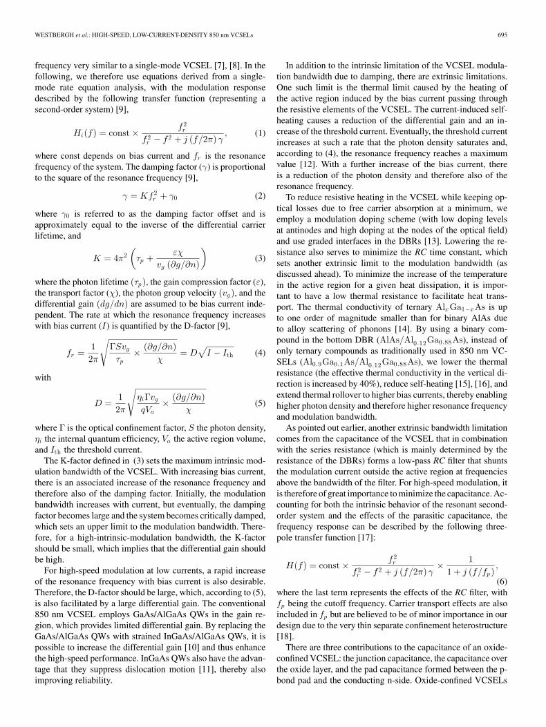
Fig. 1. Schematic cross-section of the VCSEL designed for high-speed oper-ation with double-oxide apertures and binary n-DBR.
with a single, thin oxide layer are not well suited for high-speedmodulation since the parasitic capacitance imposed by the oxide(Co ) scales with thickness (d) and area (A) of the oxide layeras Co ∝ A/d. To reduce the effective area of the oxide con-tributing to the capacitance, one option is to use a high-energyproton implant to make the majority of the VCSEL mesa insu-lating [19]. This effectively reduces the capacitance, but it addscomplexity to the VCSEL fabrication process. An alternativeapproach is to use multiple oxide layers, which reduces the ca-pacitance by effectively increasing the thickness of the oxidizedregion [20]–[22]. This simplifies fabrication since no additionalstep needs to be added to the fabrication process. We use thislatter technique in our VCSEL design with two oxide layers,separated by 100 nm, forming a 9-µm-diameter double-oxideaperture. The oxide aperture is placed in the p-DBR since oursimulations show that this provides the highest injection uni-formity due to the larger difference between vertical and lateralconductivity in the p-doped mirror stack [23]. The relativelylarge oxide aperture also helps in reducing the oxide capaci-tance, in addition to its beneficial effects on series resistance,diffraction loss, manufacturability, and reliability.
The pad capacitance is commonly kept at a minimum byreducing the area of the bond pad and inserting a thick layerof a low-k dielectric, such as polyimide or benzocyclobutene(BCB), under the bond pad. In our design, we use BCB incombination with coplanar contacts and an undoped substrateto minimize the pad capacitance. Fig. 1 shows a schematic viewof our high-speed 850 nm VCSEL design.
III. FABRICATION
Two different epitaxial structures were grown on undopedGaAs substrates by metal–organic vapor phase epitaxy. In thefirst, the active region consists of 4-nm-thick In0.07Ga0.93AsQWs separated by 6-nm-Al0.37Ga0.63As barriers, producing aphotoluminescence (PL) peak at 840 nm. The second structurehas an active region comprising 8-nm-thick GaAs QWs sep-arated by 8-nm-Al0.3Ga0.7As barriers and yields a PL peakat 835 nm. The QW widths were chosen for a gain peak at845 nm in both designs. With increasing In concentration, theQW thickness needs to be reduced and the Al concentrationin the barriers increased in order to keep the gain peak at845 nm. To maintain optical confinement, we use five QWsin the InGaAs active region compared to three in the GaAsactive region. In both structures, the p-doped top DBR con-
sists of 23 pairs of Al0.9Ga0.1As/Al0.12Ga0.88As layers. Two30-nm-thick Al0.98Ga0.02As layers, separated by 100 nm, areincluded above the active region to allow for selective oxidationand formation of a double-oxide aperture. The n-doped bot-tom DBR includes four pairs of Al0.9Ga0.1As/Al0.12Ga0.88Aslayers directly below the active region, followed by 28 pairsof AlAs/Al0.12Ga0.88As layers and finally an n-doped GaAscontact layer on the undoped substrate.
The device processing uses standard fabrication techniquesfor oxide-confined VCSELs. In the first step, a Ti/Pt/Au topring contact was deposited by e-beam evaporation. Next, a 34-µm-diameter mesa was dry etched with an inductively coupledplasma (ICP) etcher using Ar/SiCl4 and Ar/Cl2 chemistry.The etching system allows for precise depth control through alaser interferometer endpoint detection system, which is impor-tant since it is crucial to stop the etching before reaching theAlAs layers in the binary bottom DBR to avoid unintentionaloxidation. The oxide aperture was subsequently formed in awet oxidation furnace operating at a 420 C steam ambient,giving an oxidation rate of ∼0.4 µm/min. This was followedby a deeper etch down to the n-contact layer using the sameICP system. The structure was planarized using BCB, whichwas patterned to expose the n-contact layer, and Ni/Ge/Au n-contacts were deposited by e-beam evaporation and annealedin a rapid thermal processing system (RTP) for 30 s at 420 Cin an N2 ambient. Finally, Ti/Au bond pads were sputtered in aground–signal–ground (GSG) configuration, matching the GSGmicrowave probe tips with a pitch of 100 µm.
In the following section, we present a comparative study ofVCSELs with InGaAs and GaAs QWs, both with a nominaloxide aperture diameter of 9 µm. Devices with 7 µm aperturewere also investigated with very similar results in terms of bothstatic and dynamic performance. All measurements were doneon wafer without special efforts for heat sinking.
IV. STATIC PERFORMANCE CHARACTERISTICS
Figs. 2 and 3 display current–power–voltage characteristicsat different temperatures and corresponding optical spectra for9 µm oxide aperture VCSELs with InGaAs (a) and GaAs (b)QWs. The two devices show similar performance and both reacha maximum output power of 9 mW at 25 C. The InGaAsVCSEL has a threshold current of 0.6 mA and a maximumslope efficiency of 0.78 W/A, whereas the GaAs VCSEL has athreshold current of 0.4 mA and a maximum slope efficiencyof 0.71 W/A. The optical spectra show multimode operationthroughout the entire current range for both devices. The peakemission wavelength is at approximately 850 and 845 nm at 25C for the InGaAs and GaAs VCSEL, respectively, indicatingthat the detuning of the cavity resonance with respect to the gainpeak is similar (around 10 nm) in both structures.
Fig. 4 displays wall plug efficiency and differential resis-tance plotted versus bias current for both VCSELs at 25 C.The InGaAs VCSEL (Fig. 4(a)) shows a slightly higher wallplug efficiency (maximum 33% at 3.8 mA) than the GaAs VC-SEL (Fig. 4(b), maximum 29% at 5.2 mA). The differentialresistance in both devices is comparatively low for high-speed

WESTBERGH et al.: HIGH-SPEED, LOW-CURRENT-DENSITY 850 nm VCSELs 697
Fig. 2. Output power versus current at 25 C–85 C ambient temperaturetogether with voltage versus current at 25 C for the InGaAs VCSEL (a) andthe GaAs VCSEL (b).
VCSELs [2], [5], [19] because of the large aperture size. TheGaAs VCSEL resistance is stable at less than 70 Ω for biascurrents above 3 mA. For the InGaAs VCSEL, the differentialresistance is slightly higher at approximately 80 Ω at bias levelsabove 6 mA. The higher value and less stable behavior is mostlikely caused by a nonideal contact in this particular device,as the behavior of the differential resistance of other InGaAsVCSELs on the same wafer more resembles that of the GaAsVCSEL.
The thermal resistance Rth of a device is defined as thechange in temperature for a given change in power dissipationPd = IV − Pout , where I is the drive current, V is the voltagedrop, and Pout is the optical output power. Since it is diffi-cult to measure the temperature of a device directly, an indirectmethod has to be used where the emission wavelength is mea-sured under low duty cycle pulsed operation as a function of theambient (heat sink) temperature. Self-heating effects are therebyremoved, and an accurate measure of wavelength change withtemperature, ∆λ/∆T , can be deduced. By subsequently mea-suring the change of the emission wavelength as a functionof dissipated power under continuous operation, ∆λ/∆Pd , thetemperature increase can be related to the dissipated power and
Fig. 3. Optical spectra at 25 C–85 C and 5.0 mA for the InGaAs VCSEL(a) and the GaAs VCSEL (b).
the thermal resistance can be calculated as
Rth =∆T
∆Pd=
(∆λ/∆Pd)(∆λ/∆T )
. (7)
Using a pulsed current source and a Peltier element with athermistor for temperature control, the wavelength shift withtemperature was measured to be 0.062 nm/C for both the In-GaAs and GaAs VCSEL at room temperature. From this re-sult, in combination with measurements of the emission wave-length (of the longest wavelength, fundamental mode) and out-put power at various continuous bias currents, the thermal resis-tance was calculated to be 1.9 C/mW for both VCSELs using(7). This value is lower than the thermal resistance reported forcomparable on-wafer VCSELs with all-ternary DBRs, e.g., [24](10 µm oxide aperture, Rth = 2.65C/mW), but higher thanvalues for, e.g., designs where Cu plating is used for improvedheat transport [25] (Rth ≈ 1.0C/mW for a 9 µm oxide aper-ture). Metal plating, however, introduces an additional parasiticcapacitance that adds to the total pad capacitance, and thus, thereis a tradeoff to consider when using this technique in devicesintended for high-speed operation.
698 IEEE JOURNAL OF SELECTED TOPICS IN QUANTUM ELECTRONICS, VOL. 15, NO. 3, MAY/JUNE 2009
Fig. 4. Wall plug efficiency (WPE) and differential resistance at 25 C plottedversus bias current for (a) the InGaAs VCSEL and (b) the GaAs VCSEL.
V. DYNAMIC PERFORMANCE CHARACTERISTICS
A. Small-Signal Modulation Response
To determine the device bandwidth, small-signal modula-tion response (S21) measurements were conducted using a 65GHz network analyzer (Anritsu 37397 C). The bias currentwas combined with the RF modulation signal using a high-frequency bias-T and fed to the VCSEL under test through ahigh-frequency microwave probe (Picoprobe 40 A-GSG-100-P). A Peltier element and a thermistor attached to the VCSELsubmount were used to control the ambient operating tempera-ture of the VCSEL. Optical feedback was avoided by couplingthe output beam via an antireflection (AR) coated lens systemto a multimode fiber tilted at a 10 angle. A 25 GHz multi-mode photodetector (New Focus 1481-S-50) was used to detectthe signal, and corrections for the frequency response of thedetector were made before analyzing the data.
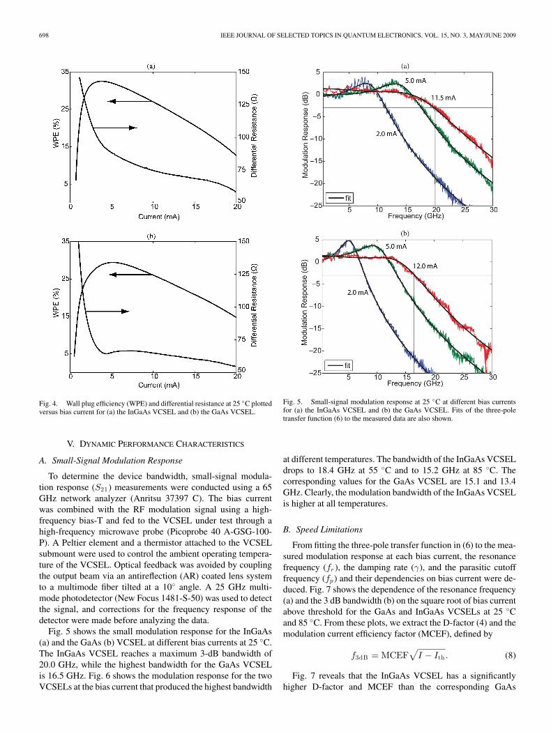
Fig. 5 shows the small modulation response for the InGaAs(a) and the GaAs (b) VCSEL at different bias currents at 25 C.The InGaAs VCSEL reaches a maximum 3-dB bandwidth of20.0 GHz, while the highest bandwidth for the GaAs VCSELis 16.5 GHz. Fig. 6 shows the modulation response for the twoVCSELs at the bias current that produced the highest bandwidth
Fig. 5. Small-signal modulation response at 25 C at different bias currentsfor (a) the InGaAs VCSEL and (b) the GaAs VCSEL. Fits of the three-poletransfer function (6) to the measured data are also shown.
at different temperatures. The bandwidth of the InGaAs VCSELdrops to 18.4 GHz at 55 C and to 15.2 GHz at 85 C. Thecorresponding values for the GaAs VCSEL are 15.1 and 13.4GHz. Clearly, the modulation bandwidth of the InGaAs VCSELis higher at all temperatures.
B. Speed Limitations
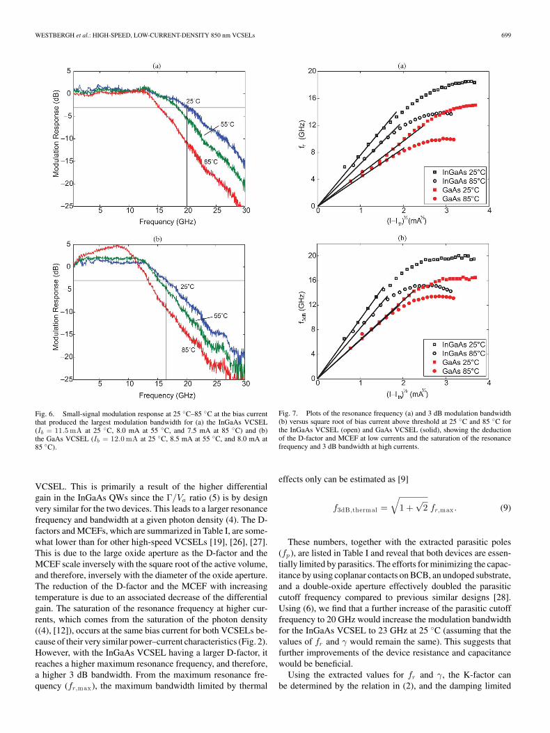
From fitting the three-pole transfer function in (6) to the mea-sured modulation response at each bias current, the resonancefrequency (fr ), the damping rate (γ), and the parasitic cutofffrequency (fp ) and their dependencies on bias current were de-duced. Fig. 7 shows the dependence of the resonance frequency(a) and the 3 dB bandwidth (b) on the square root of bias currentabove threshold for the GaAs and InGaAs VCSELs at 25 Cand 85 C. From these plots, we extract the D-factor (4) and themodulation current efficiency factor (MCEF), defined by
f3dB = MCEF√
I − Ith . (8)
Fig. 7 reveals that the InGaAs VCSEL has a significantlyhigher D-factor and MCEF than the corresponding GaAs
WESTBERGH et al.: HIGH-SPEED, LOW-CURRENT-DENSITY 850 nm VCSELs 699
Fig. 6. Small-signal modulation response at 25 C–85 C at the bias currentthat produced the largest modulation bandwidth for (a) the InGaAs VCSEL(Ib = 11.5 mA at 25 C, 8.0 mA at 55 C, and 7.5 mA at 85 C) and (b)the GaAs VCSEL (Ib = 12.0 mA at 25 C, 8.5 mA at 55 C, and 8.0 mA at85 C).
VCSEL. This is primarily a result of the higher differentialgain in the InGaAs QWs since the Γ/Va ratio (5) is by designvery similar for the two devices. This leads to a larger resonancefrequency and bandwidth at a given photon density (4). The D-factors and MCEFs, which are summarized in Table I, are some-what lower than for other high-speed VCSELs [19], [26], [27].This is due to the large oxide aperture as the D-factor and theMCEF scale inversely with the square root of the active volume,and therefore, inversely with the diameter of the oxide aperture.The reduction of the D-factor and the MCEF with increasingtemperature is due to an associated decrease of the differentialgain. The saturation of the resonance frequency at higher cur-rents, which comes from the saturation of the photon density((4), [12]), occurs at the same bias current for both VCSELs be-cause of their very similar power–current characteristics (Fig. 2).However, with the InGaAs VCSEL having a larger D-factor, itreaches a higher maximum resonance frequency, and therefore,a higher 3 dB bandwidth. From the maximum resonance fre-quency (fr,max ), the maximum bandwidth limited by thermal
Fig. 7. Plots of the resonance frequency (a) and 3 dB modulation bandwidth(b) versus square root of bias current above threshold at 25 C and 85 C forthe InGaAs VCSEL (open) and GaAs VCSEL (solid), showing the deductionof the D-factor and MCEF at low currents and the saturation of the resonancefrequency and 3 dB bandwidth at high currents.
effects only can be estimated as [9]
f3dB ,thermal =√
1 +√
2 fr,max . (9)
These numbers, together with the extracted parasitic poles(fp ), are listed in Table I and reveal that both devices are essen-tially limited by parasitics. The efforts for minimizing the capac-itance by using coplanar contacts on BCB, an undoped substrate,and a double-oxide aperture effectively doubled the parasiticcutoff frequency compared to previous similar designs [28].Using (6), we find that a further increase of the parasitic cutofffrequency to 20 GHz would increase the modulation bandwidthfor the InGaAs VCSEL to 23 GHz at 25 C (assuming that thevalues of fr and γ would remain the same). This suggests thatfurther improvements of the device resistance and capacitancewould be beneficial.
Using the extracted values for fr and γ, the K-factor canbe determined by the relation in (2), and the damping limited
700 IEEE JOURNAL OF SELECTED TOPICS IN QUANTUM ELECTRONICS, VOL. 15, NO. 3, MAY/JUNE 2009
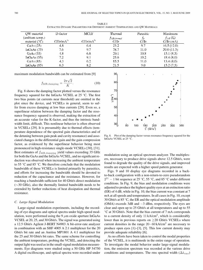
TABLE IEXTRACTED DYNAMIC PARAMETERS FOR DIFFERENT AMBIENT TEMPERATURES AND QW MATERIALS
maximum modulation bandwidth can be estimated from [9]
f3dB ,damping =2π
√2
K. (10)
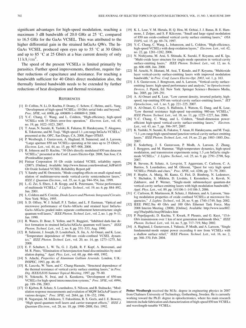
Fig. 8 shows the damping factor plotted versus the resonancefrequency squared for the InGaAs VCSEL at 25 C. The firsttwo bias points (at currents near threshold) are omitted in theplot since the device, and VCSELs in general, seem to suf-fer from excess damping at low bias currents [29]. Even so, asuperlinear relation between the damping factor and the reso-nance frequency squared is observed, making the extraction ofan accurate value for the K-factor, and thus the intrinsic band-width limit, difficult. This nonlinear behavior is often observedin VCSELs [29]. It is presumably due to thermal effects (tem-perature dependence of the spectral gain characteristics and ofthe detuning between gain peak and cavity resonance) and asso-ciated changes in the differential gain and the gain compressionfactor, as evidenced by the superlinear behavior being mostpronounced in high-resistance single-mode VCSELs [30], [31].Best estimates of f3dB ,damping yield values exceeding 35 GHzfor both the GaAs and the InGaAs VCSEL, and no significant re-duction was observed when increasing the ambient temperatureto 55 C and 85 C. We therefore conclude that the modulationbandwidth of these VCSELs is limited primarily by parasitics,and efforts for increasing the bandwidth should be devoted toreduction of the capacitance and the resistance. However, forreaching a bandwidth sufficient for 40 Gbit/s direct modulation(∼30 GHz), also the thermally limited bandwidth needs to beextended by further reductions of heat dissipation and thermalresistance.
C. Large-Signal Modulation
Large-signal modulation experiments, including the record-ing of eye diagrams and optical spectra under high-speed mod-ulation, were performed using the 9 µm oxide aperture InGaAsVCSEL at 20, 25, and 30 Gbit/s. The signal was generated usinga 12.5 Gbit/s Agilent J-BERT N4903 A bit-error-rate analyzerin combination with an SHF 4005 A 2:1 multiplexer for the 20Gbit/s bit rate and an Anritsu MP1801 A 4:1 multiplexer forthe 25 and 30 Gbit/s bit rates. The same scheme for controllingthe ambient temperature, probing the VCSEL, and detecting theoutput light was used as in the small-signal modulation measure-ments. Eye diagrams were studied using a 50 GHz HP 54750A digital oscilloscope, and optical spectra were recorded under
Fig. 8. Plot of the damping factor versus resonance frequency squared for theInGaAs VCSEL at 25 C.
modulation using an optical spectrum analyzer. The multiplex-ers, necessary to produce drive signals above 12.5 Gbit/s, werefound to degrade the quality of the drive signals, and improvedresults are expected with a higher speed pattern generator.
Figs. 9 and 10 display eye diagrams recorded in a back-to-back configuration with a non-return-to-zero pseudorandom231 − 1 bit sequence at 25 C, 55 C, and 85 C under differentconditions. In Fig. 9, the bias and modulation conditions wereadjusted to produce the highest quality eyes at an extinction ratio(ER) of 4 dB, while in Fig. 10, the bias current was constant at 7mA at all speeds and temperatures. In all cases in Fig. 10, except30 Gbit/s at 85 C, the ER and the optical modulation amplitude(OMA) exceeds 3dB and −3 dBm, respectively. The eyes areclear and open up to 25 Gbit/s at all temperatures and up to 55C at 30 Gbit/s. Note that the bias current of 7 mA correspondsto a current density of only 11 kA/cm2 , which is considerablylower than in previous reports on ≥20 Gbit/s VCSELs wherecurrent densities in the range 20−60 kA/cm2 are necessary toproduce open eyes [1]–[3], [5]. This low current density mayprovide adequate reliability [6].
As no efforts have been taken to control the modal propertiesof the VCSEL, it is multimode in the entire range of operation.To investigate the modal behavior under large-signal modula-tion, the emission spectrum was recorded at the various driveconditions and temperatures. The rms spectral width (∆λrms)

WESTBERGH et al.: HIGH-SPEED, LOW-CURRENT-DENSITY 850 nm VCSELs 701
Fig. 9. Eye diagrams at 20–30 Gbit/s modulation for the InGaAs VCSEL at 25 C–85 C at a constant ER of 4.0 dB. The modulation power and bias current areindicated at each eye diagram.
Fig. 10. Eye diagrams at 20–30 Gbit/s modulation for the InGaAs VCSEL at 25 C–85 C at a constant bias current of 7.0 mA. The modulation power and ERare indicated at each eye diagram.
was then calculated from
∆λrms =√∑
(λi − λ0)2 pi∑pi
, λ0 =∑
λipi∑pi
, (11)
where λ0 is the mean wavelength and pi is the power at aparticular wavelength λi . Values from 0.45 to 0.39 nm wereobtained under the constant bias condition, which is within therange considered acceptable for future standards [32]. However,chromatic dispersion could potentially become a limiting factorwhen propagating the signal over long distances of multimodefiber [33]. If a reduction of the spectral rms width is needed,there is the possibility of integrating a mode filter in the topDBR using the surface relief technology to reduce the numberof transverse modes [34].
VI. CONCLUSION
We have investigated the small- and large-signal modula-tion characteristics of oxide confined, multimode 850 nm VC-SELs and compared the performance of devices with InGaAsand GaAs QWs in the active region. Both designs were op-timized for high-speed performance using modulation dopingand graded interfaces in the DBRs to reduce resistance; binaryAlAs in the bottom DBR to reduce thermal resistance; and adouble-oxide aperture, coplanar contacts, and an undoped sub-strate to minimize capacitance. The large aperture (9 µm) im-proves manufacturability and enables a low current density forreliable operation. The static performance was similar for bothdevices, demonstrating a maximum output power of 9 mW andthermal resistances of 1.9 C/mW. The InGaAs VCSEL showed
702 IEEE JOURNAL OF SELECTED TOPICS IN QUANTUM ELECTRONICS, VOL. 15, NO. 3, MAY/JUNE 2009
significant advantages for high-speed modulation, reaching amaximum 3 dB bandwidth of 20.0 GHz at 25 C, comparedto 16.5 GHz for the GaAs VCSEL. This was attributed to thehigher differential gain in the strained InGaAs QWs. The In-GaAs VCSEL produced open eyes up to 55 C at 30 Gbit/sand up to 85 C at 25 Gbit/s at a bias current density of only11 kA/cm2 .
The speed of the present VCSELs is limited primarily byparasitics. Further speed improvements, therefore, require fur-ther reductions of capacitance and resistance. For reaching abandwidth sufficient for 40 Gbit/s direct modulation also, thethermally limited bandwidth needs to be extended by furtherreductions of heat dissipation and thermal resistance.
REFERENCES
[1] D. Collins, N. Li, D. Kuchta, F. Doany, C. Schow, C. Helms, and L. Yang,“Development of high-speed VCSELs: 10 Gb/s serial links and beyond,”Proc. SPIE, vol. 6908, pp. 690809-1–690809-9, 2008.
[2] Y.-C. Chang, C. Wang, and L. Coldren, “High-efficiency, high-speedVCSELs with 35 Gbit/s error-free operation,” Electron. Lett., vol. 43,no. 19, pp. 1022–1023, 2007.
[3] T. Anan, N. Suzuki, K. Yashiki, K. Fukatsu, H. Hatakeyama, T. Akagawa,K. Tokutome, and M. Tsuji, “High-speed 1.1-µm range InGaAs VCSELs,”presented at the, OFC, San Diego, CA, 2008, Paper OThS5.
[4] P. Westbergh, J. Gustavsson, A. Haglund, H. Sunnerud, and A. Larsson,“Large aperture 850 nm VCSELs operating at bit rates up to 25 Gbit/s,”Electron. Lett., vol. 44, no. 15, pp. 907–908, 2008.
[5] R. Johnson and D. Kuchta, “30 Gb/s directly modulated 850 nm datacomVCSELs,” presented at the Conf. Lasers Electro-Opt. 2008, San Jose, CA(Postdeadline paper).
[6] Finisar Corporation 10 Gb oxide isolated VCSEL reliability report.(2007). [Online]. Available: http://www.finisar.com/download_6iJFn610Gb Oxide Isolated VCSEL Reliability Report.pdf
[7] Y. Satuby and M. Orenstein, “Mode-coupling effects on small-signal mod-ulation of multitransverse-mode vertical-cavity semiconductor lasers,”IEEE J. Quantum Electron., vol. 35, no. 6, pp. 944–954, Jun. 1999.
[8] L.-G. Zei, S. Ebers, J.-R. Kropp, and K. Petermann, “Noise performanceof multimode VCSELs,” J. Lightw. Technol., vol. 19, no. 6, pp. 884–892,Jun. 2001.
[9] L. Coldren and S. Corzine, Diode Lasers and Photonic Integrated Circuits.New York: Wiley, 1995.
[10] S. D. Offsey, W. J. Schaff, P. J. Tasker, and L. F. Eastman, “Optical andmicrowave performance of GaAs-AlGaAs and strained layer InGaAs-GaAs-AlGaAs graded index separate confinement heterostructure singlequantum well lasers,” IEEE Photon. Technol. Lett., vol. 2, no. 1, pp. 9–11,Jan. 1990.
[11] R. Waters, D. Bour, S. Yellen, and N. Ruggieri, “Inhibited dark-line de-fect formation in strained InGaAs/AlGaAs quantum well lasers,” IEEEPhoton. Technol. Lett., vol. 2, no. 8, pp. 531–533, Aug. 1990.
[12] R. Safaisini, J. Joseph, D. Louderback, X. Jin, A. Al-Omari, and K. Lear,“Temperature dependence of 980-nm oxide-confined VCSEL dynam-ics,” IEEE Photon. Technol. Lett., vol. 20, no. 14, pp. 1273–1275, Jul.2008.
[13] E. F. Schubert, L. W. Tu, G. J. Zydik, R. F. Kopf, A. Benvenuti, andM. R. Pinto, “Elimination of heterojunction band discontinuities by mod-ulation doping,” Appl. Phys. Lett., vol. 60, pp. 466–468, 1992.
[14] S. Adachi, Properties of Aluminum Gallium Arsenide. London, U.K.:INSPEC, 1993, pp. 46–49.
[15] K. Lascola, W. Yuen, and C. Chang-Hasnain, “Structural dependence ofthe thermal resistance of vertical cavity surface emitting lasers,” in Proc.Dig. IEEE/LEOS Summer Topical Meeting, 1997, pp. 79–80.
[16] N. Yokouchi, N. Iwai, and A. Kasukawa, “Development of 850-nmVCSELs for high-speed interconnection systems,” Proc. SPIE, vol. 4994,pp. 189–196, 2003.
[17] O. Kjebon, R. Schatz, S. Lourdudoss, S. Nilsson, and B. Stalnacke, “Mod-ulation response measurements and evalution of MQW InGaAsP lasers ofvarious designs,” Proc. SPIE, vol. 2684, pp. 138–152, 1996.
[18] R. Nagarajan, M. Ishikawa, T. Fukushima, R. S. Geels, and J. E. Bowers,“High speed quantum-well lasers and carrier transport effects,” IEEE J.Quantum Electron., vol. 28, no. 10, pp. 1990–2008, Oct. 1992.
[19] K. L. Lear, V. M. Hietala, H. Q. Hou, M. Ochiai, J. J. Banas, B. E. Ham-mons, J. Zolper, and S. P. Kilcoyne, “Small and large signal modulationof 850 nm oxide-confined vertical cavity surface emitting lasers,” OSATOPS, vol. 15, pp. 69–74, 1997.
[20] Y.-C. Chang, C. Wang, L. Johansson, and L. Coldren, “High-efficiency,high-speed VCSELs with deep oxidation layers,” Electron. Lett., vol. 42,no. 22, pp. 1281–1282, 2006.
[21] N. Nishiyama, M. Arai, S. Shinada, K. Suzuki, F. Koyama, and K. Iga,“Multi-oxide layer structure for single-mode operation in vertical-cavitysurface-emitting lasers,” IEEE Photon. Technol. Lett., vol. 12, no. 6,pp. 606–608, Jun. 2000.
[22] M. Azuchi, N. Jikutani, M. Arai, T. Kondo, and F. Koyama, “Multioxidelayer vertical-cavity surface-emitting lasers with improved modulationbandwidth,” in Proc. Conf. Lasers Electro-Opt. 2003, vol. 1, p. 163.
[23] J. S. Gustavsson, J. Bengtsson, and A. Larsson, “Vertical-cavity surface-emitting lasers: high-speed performance and analysis,” in OptoelectronicDevices, J. Piprek, Ed. New York: Springer Science+Business Media,Inc. 2005, pp. 249–291.
[24] A. Al-Omari and K. Lear, “Low current density, inverted polarity, high-speed, top-emitting 850 nm vertical-cavity surface-emitting lasers,” IETOptoelectron., vol. 1, no. 5, pp. 221–225, 2007.
[25] A. Al-Omari, G. Carey, S. Hallstein, J. Watson, G. Dang, and K. Lear,“Low thermal resistance high-speed top-emitting 980-nm VCSELs,”IEEE Photon. Technol. Lett., vol. 18, no. 11, pp. 1225–1227, Jun. 2006.
[26] Y.-C. Chang, C. Wang, and L. Coldren, “Small-dimension power-efficient high-speed vertical-cavity surface-emitting lasers,” Electron.Lett., vol. 43, no. 7, pp. 396–397, 2007.
[27] K. Yashiki, N. Suzuki, K. Fukatsu, T. Anan, H. Hatakeyama, and M. Tsuji,“1.1-µm-range high-speed tunnel junction vertical-cavity surface-emittinglasers,” IEEE Photon. Technol. Lett., vol. 19, no. 23, pp. 1883–1885, Dec.2007.
[28] E. Soderberg, J. S. Gustavsson, P. Modh, A. Larsson, Z. Zhang,J. Berggren, and M. Hammar, “High-temperature dynamics, high-speedmodulation, and transmission experiments using 1.3 µm InGaAs single-mode VCSELs,” J. Lightw. Technol., vol. 25, no. 9, pp. 2791–2798, Sep.2007.
[29] R. Stevens, R. Schatz, A. Lovqvist, T. Aggerstam, C. Carlsson, C. A.Barrios, S. Lourdudoss, and M. Ghisoni, “Quest for very high speedVCSELs: Pitfalls and clues,” Proc. SPIE, vol. 4286, pp. 71–79, 2001.
[30] F. Hopfer, A. Mutig, M. Kuntz, G. Fiol, D. Bimberg, N. Ledentsov,V. Shchukin, S. Mikhrin, D. Livshits, I. Krestnikov, A. Kovsh, N.Zakharov, and P. Werner, “Single-mode submonolayer quantum-dotvertical-cavity surface-emitting lasers with high modulation bandwidth,”Appl. Phys. Lett., vol. 89, pp. 141106-1–141106-3, 2006.
[31] C. Carlsson, H. Martinsson, R. Schatz, J. Halonen, and A. Larsson, “Ana-log modulation properties of oxide confined VCSELs at microwave fre-quencies,” J. Lightw. Technol., vol. 20, no. 9, pp. 1740–1749, Sep. 2002.
[32] IEEE P802.3ba 40 Gb/s and 100 Gb/s Ethernet Task Force, May2008 Interim Meeting. (2008). [Online]. Available: http://www.ieee802.org/3/ba/public/may08/index.htm
[33] P. Pepeljugoski, D. Kuchta, Y. Kwark, P. Pleunis, and G. Kuyt, “15.6-Gb/s transmission over 1 km of next generation multimode fiber,” IEEEPhoton. Technol. Lett., vol. 14, no. 5, pp. 717–719, May 2002.
[34] A. Haglund, J. Gustavsson, J. Vukusic, P. Modh, and A. Larsson, “Singlefundamental-mode output power exceeding 6 mw from VCSELs witha shallow surface relief,” IEEE Photon. Technol. Lett., vol. 16, no. 2,pp. 368–370, Feb. 2004.
Petter Westbergh received the M.Sc. degree in engineering physics in 2007from Chalmers University of Technology, Gothenburg, Sweden. He is currentlyworking toward the Ph.D. degree in optoelectronics, where his main researchinterests include fabrication and characterization of high-speed 850 nm VCSELsand wavelength-tunable VCSELs.
WESTBERGH et al.: HIGH-SPEED, LOW-CURRENT-DENSITY 850 nm VCSELs 703
Johan S. Gustavsson received the M.Sc. degree in electrical engineering in1998 and the Ph.D. degree in photonics in 2003 from Chalmers University ofTechnology, Gothenburg, Sweden.
His Ph.D. thesis dealt with mode dynamics and noise in VCSELs. He iscurrently an Assistant Professor at the Photonics Laboratory, Department ofMicrotechnology and Nanoscience, Chalmers University of Technology. Hiscurrent research interests include design, modeling, and characterization of long-wavelength semiconductor lasers, mode and polarization control in VCSELsusing shallow surface structures, and improving the bandwidth of conventionalGaAs-based VCSELs.
Asa Haglund received the M.Sc. degree in physics from Gothenburg University,Gothenburg, Sweden, in 2000, and the Ph.D. degree in electrical engineeringfrom Chalmers University of Technology, Gothenburg, in 2005. Her Ph.D. thesiswas titled “Mode and polarization control in VCSELs using surface structures.”Since 2008, she has been an Assistant Professor at the Photonics Laboratory, De-partment of Microtechnology and Nanoscience, Chalmers University of Tech-nology. Her current research interests include tunable VCSELs using MicroElectro Mechanical System structures, high-speed GaAs-based VCSELs anddeep-UV-light emitters.
Mats Skold received the M.Sc. and Ph.D. degrees in electrical engineeringfrom the Chalmers University of Technology, Gothenburg, Sweden, in 2001and 2008, respectively.
He is currently with the Photonics Laboratory, Chalmers University of Tech-nology. His current research interests include advanced modulation formats,optical coherent systems, characterization of optical signals, and optical net-work monitoring.
Andrew Joel, photograph and biography not available at the time of publication.
Anders Larsson (S’96–M’01) received the M.Sc. and Ph.D. degrees in electricalengineering from Chalmers University of Technology, Gothenburg, Sweden, in1982 and 1987, respectively.
In 1991, he joined the faculty at Chalmers University of Technology, wherehe was promoted to Professor in 1994. From 1984 to 1985, he was with theDepartment of Applied Physics, California Institute of Technology, and from1988 to 1991, with the Jet Propulsion Laboratory, both at Pasadena, CA. Hehas been a Guest Professor at Ulm University, Ulm, Germany, at the OpticalScience Center, University of Arizona, Tucson, and at Osaka University, Osaka,Japan. He is presently a Guest Professor at the Institute of Semiconductors,Chinese Academy of Sciences, Beijing, China. He has authored or coauthoredmore than 200 papers in scientific journals and 190 conference papers. Hiscurrent research interests include VCSELs, optically pumped semiconductordisk lasers, and emitters in wide-bandgap materials.
Prof. Larsson coorganized the IEEE Semiconductor Laser Workshop 2004,organized the European Semiconductor Laser Workshop 2004, and was theProgram Chair for the IEEE International Semiconductor Laser Conference2006 and the General Chair for the same conference in 2008. His scientificbackground is in the areas of materials and devices for optical communication,optical information processing, infrared detection, and optical measurements.He is a Fellow of the European Optical Society.
Related Documents


![1060 nm GaAs VCSELs for Extended Reach Optical ... · 1060 nm GaAs VCSELs for Extended Reach Optical Interconnects in Data Centers Ewa Simpanen ... standards for 500 m and above [12].](https://static.cupdf.com/doc/110x72/5e499564235f120ea07cdf96/1060-nm-gaas-vcsels-for-extended-reach-optical-1060-nm-gaas-vcsels-for-extended.jpg)