NEW CONCEPT OF 3.2{4.8GHz IMPULSE
GENERATOR FOR UWB TRANSMITTER¤
DALENDA BEN ISSAy
University Laboratory LETI-ENIS,
University of Sfax, Sfax, Street of Soukra 3Km,BP.3038, Tunisia
ABDENNACEUR KACHOURIz and MOUNIR SAMETx
LETI-ENIS, University of Sfax,Sfax, Street of Soukra 3Km, BP.3038, Tunisia
ydalenda [email protected]@enis.rnu.tn
Received 2 March 2010
Accepted 22 October 2010
A new design of Ultra-Wide band (UWB) generator is described in this paper. The UWB
impulse generator circuit is the most essential block in a mono-band UWB transmitter. The
proposed ultra wide band impulse generator circuit utilizes the performances of the CMOStechnology e®ectively, it is composed of a voltage controlled oscillator (VCO), and a rectangular
pulse generator (RPG) and mixer. The RPG circuit consists of a frequency divider 1/128 circuit,
time delay, N-inverters and AND gate function. The impulse UWB generator is based on the
rectangular pulse modulated with the aim of generating the UWB impulse signal. This proposedcircuit generates an output signal which is de¯ned by the bandwidth of 1.6GHz at centered
frequency of 4GHz and the limited Power Spectral Density (PSD) is �41:47 dBm=MHz. The
peak-to-peak amplitude of the UWB impulse signal is 528mV, the output impulse width of 2 ns
and the impulse repetition period (PRP) is 32 ns. The power consumption is about 12.5mW at2.5V voltage supply.
Keywords: UWB transmitter architecture; UWB impulse generator; voltage controlledoscillator; mixer; rectangular pulse generator.
1. Introduction
Recent research into the design of Ultra-Wide Band (UWB) transceiver architecture
show several types of UWB technology such as Direct-Sequence UWB (DS-UWB),
Impulse Radio (IR) and Multi-Band Orthogonal Frequency Division Multiplexing
(MB-OFDM).1,2 While the DS-UWB and MB-OFDM are potential applicants for
*This paper was recommended by Regional Editor Piero Malcovati.
Journal of Circuits, Systems, and ComputersVol. 20, No. 2 (2011) 313�327
#.c World Scienti¯c Publishing Company
DOI: 10.1142/S021812661100727X
313
February 25, 2011 10:48:52am WSPC/123-JCSC 00727 ISSN: 0218-1266
wireless personal area network (WPAN) applications, IR has also been attractive for
imaging system and radar system applications.1�10 The Federal Communications
Commission (FCC) de¯nes a UWB signal by spectrum bandwidth superior to 1.5GHz
and Power Spectral Density (PSD) limited to �41:3 dBm=MHz.11 Di®erent archi-
tecture of UWB transceivers presented in recent publications agree with these strict
limitations.1�10,12�16 In this viewpoint, a particular type of UWB signal, Impulse
Radio (IR-UWB) uses a short pulse and has the capability of reducing the cost and size
of integration.
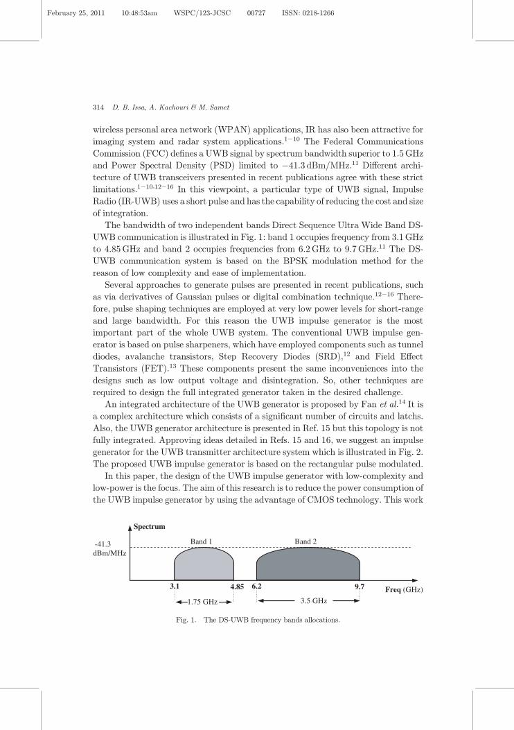
The bandwidth of two independent bands Direct Sequence Ultra Wide Band DS-
UWB communication is illustrated in Fig. 1: band 1 occupies frequency from 3.1GHz
to 4.85GHz and band 2 occupies frequencies from 6.2GHz to 9.7GHz.11 The DS-
UWB communication system is based on the BPSK modulation method for the
reason of low complexity and ease of implementation.
Several approaches to generate pulses are presented in recent publications, such
as via derivatives of Gaussian pulses or digital combination technique.12�16 There-
fore, pulse shaping techniques are employed at very low power levels for short-range
and large bandwidth. For this reason the UWB impulse generator is the most
important part of the whole UWB system. The conventional UWB impulse gen-
erator is based on pulse sharpeners, which have employed components such as tunnel
diodes, avalanche transistors, Step Recovery Diodes (SRD),12 and Field E®ect
Transistors (FET).13 These components present the same inconveniences into the
designs such as low output voltage and disintegration. So, other techniques are
required to design the full integrated generator taken in the desired challenge.
An integrated architecture of the UWB generator is proposed by Fan et al.14 It is
a complex architecture which consists of a signi¯cant number of circuits and latchs.
Also, the UWB generator architecture is presented in Ref. 15 but this topology is not
fully integrated. Approving ideas detailed in Refs. 15 and 16, we suggest an impulse
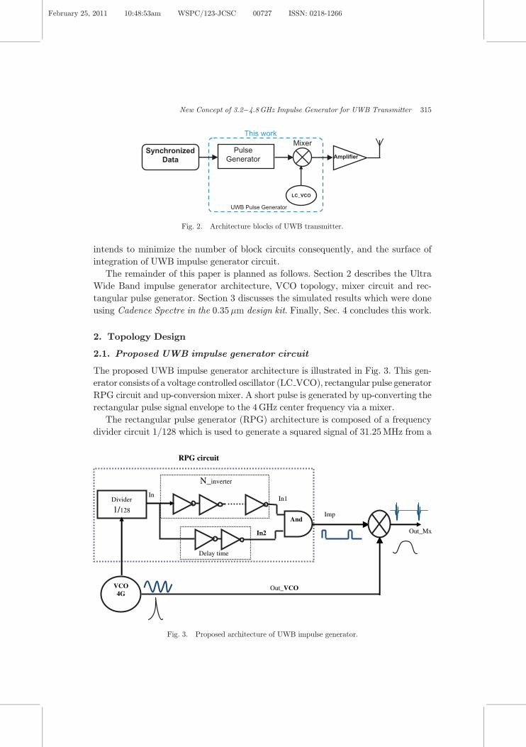
generator for the UWB transmitter architecture system which is illustrated in Fig. 2.
The proposed UWB impulse generator is based on the rectangular pulse modulated.
In this paper, the design of the UWB impulse generator with low-complexity and
low-power is the focus. The aim of this research is to reduce the power consumption of
the UWB impulse generator by using the advantage of CMOS technology. This work
Band 1 Band 2-41.3 dBm/MHz
Freq (GHz)
Spectrum
1.75 GHz 3.5 GHz
3.1 4.85 6.2 9.7
Fig. 1. The DS-UWB frequency bands allocations.
314 D. B. Issa, A. Kachouri & M. Samet
February 25, 2011 10:48:53am WSPC/123-JCSC 00727 ISSN: 0218-1266
intends to minimize the number of block circuits consequently, and the surface of
integration of UWB impulse generator circuit.
The remainder of this paper is planned as follows. Section 2 describes the Ultra
Wide Band impulse generator architecture, VCO topology, mixer circuit and rec-
tangular pulse generator. Section 3 discusses the simulated results which were done
using Cadence Spectre in the 0:35�m design kit. Finally, Sec. 4 concludes this work.
2. Topology Design
2.1. Proposed UWB impulse generator circuit
The proposed UWB impulse generator architecture is illustrated in Fig. 3. This gen-
erator consists of a voltage controlled oscillator (LC VCO), rectangular pulse generator
RPG circuit and up-conversion mixer. A short pulse is generated by up-converting the
rectangular pulse signal envelope to the 4GHz center frequency via a mixer.
The rectangular pulse generator (RPG) architecture is composed of a frequency
divider circuit 1/128 which is used to generate a squared signal of 31.25MHz from a
LC_VCO
Amplifier
This work
SynchronizedData
PulseGenerator
UWB Pulse Generator
Mixer
Fig. 2. Architecture blocks of UWB transmitter.
RPG circuit
Out_VCO
Out_Mx
Imp
Delay time
In In1
In2
VCO4G
Divider
1/128
N_inverter
And
Fig. 3. Proposed architecture of UWB impulse generator.
New Concept of 3.2�4.8GHz Impulse Generator for UWB Transmitter 315
February 25, 2011 10:48:53am WSPC/123-JCSC 00727 ISSN: 0218-1266
VCO output signal of 4GHz, delay time, N-inverters, and \AND" logic circuit. The
rectangular pulse generator produces the signal \Imp" de¯ned by the °owing
expression,
ImpðtÞ ¼ 1 if 0 < t < Ppulse ;
0 if Ppulse < t < PRP :
�ð1Þ
In this work, we take Ppulse ¼ 1 ns and PRP ¼ 32 ns.
Where PRP is the pulse repetition period, and Ppulse is the period when the signal
is equal to 1. In this work, the PRP is equal to 32 ns and the pulse repetition
frequency (PRF) is 31.25MHz.
The output signal of LC VCO circuit \Out VCO" is de¯ned by this expression,
Out VCOðtÞ ¼ ALO cosð!LOtÞ ; ð2Þwhere ALO and !LO are the amplitude and the pulsation of LC VCO output signal,
respectively.
By multiplying the output signal of LC VCO and rectangular pulse generator, the
up-convert mixer generates an impulse signal (Out Mx) envelope to the VCO cen-
tered frequency f 0 and it is de¯ned by the following expression,
Out MxðtÞ ¼ALO cosðð!LO þ !PRÞtÞ if 0 < t < Ppulse ;
0 if Ppulse < t < PRP :
(ð3Þ
From expression (3) the output signal of the UWB generator, one pulse is trans-
mitted every 32 ns. The output spectrum of this generator shows large bandwidth
occupation which is more than 1.5GHz.
The most important advantages of the UWB impulse generator are its low
number of blocks and low complexity, and it being fully integrated. It is also simple
to convert the UWB generator into a multi-bands architecture UWB transmitter. In
addition to that, the proposed generator consumes minimum power via using CMOS
technology. All size components are optimized to obtain suitable results.
2.2. VCO architecture
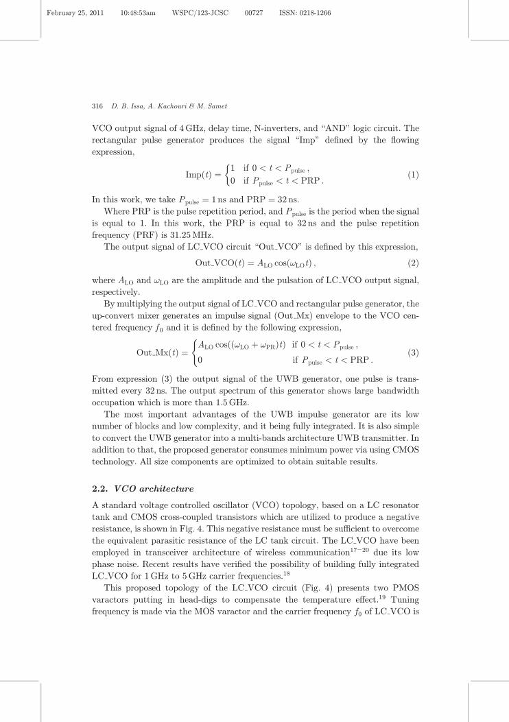
A standard voltage controlled oscillator (VCO) topology, based on a LC resonator
tank and CMOS cross-coupled transistors which are utilized to produce a negative
resistance, is shown in Fig. 4. This negative resistance must be su±cient to overcome
the equivalent parasitic resistance of the LC tank circuit. The LC VCO have been
employed in transceiver architecture of wireless communication17�20 due its low
phase noise. Recent results have veri¯ed the possibility of building fully integrated
LC VCO for 1GHz to 5GHz carrier frequencies.18
This proposed topology of the LC VCO circuit (Fig. 4) presents two PMOS
varactors putting in head-digs to compensate the temperature e®ect.19 Tuning
frequency is made via the MOS varactor and the carrier frequency f0 of LC VCO is
316 D. B. Issa, A. Kachouri & M. Samet
February 25, 2011 10:48:53am WSPC/123-JCSC 00727 ISSN: 0218-1266
de¯ned by this expression,
f0 ¼1
2�ffiffiffiffiffiffiffiffiffiffiffiffiffiffiffiffiffiffiffiffiffiLtankCtank
p ; ð4Þ
where C tank and Ltank are the equivalent capacitance and inductance of LC VCO
circuit, respectively.
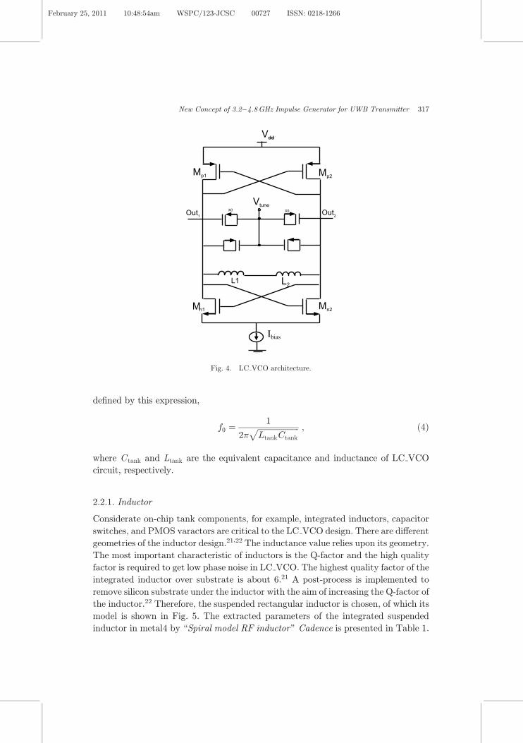
2.2.1. Inductor
Considerate on-chip tank components, for example, integrated inductors, capacitor
switches, and PMOS varactors are critical to the LC VCO design. There are di®erent
geometries of the inductor design.21,22 The inductance value relies upon its geometry.
The most important characteristic of inductors is the Q-factor and the high quality
factor is required to get low phase noise in LC VCO. The highest quality factor of the
integrated inductor over substrate is about 6.21 A post-process is implemented to
remove silicon substrate under the inductor with the aim of increasing the Q-factor of
the inductor.22 Therefore, the suspended rectangular inductor is chosen, of which its
model is shown in Fig. 5. The extracted parameters of the integrated suspended
inductor in metal4 by \Spiral model RF inductor" Cadence is presented in Table 1.
VtuneX0 X0
Mn1 Mn2
L1 L2
Mp1 Mp2
Out1Out2
Ibias
Vdd
Fig. 4. LC VCO architecture.
New Concept of 3.2�4.8GHz Impulse Generator for UWB Transmitter 317
February 25, 2011 10:48:54am WSPC/123-JCSC 00727 ISSN: 0218-1266

2.2.2. VCO design constraints
The LC VCO design constraints are the start-up condition, tuning range, tank
amplitude, power consumption and phase noise. The graphical optimization method
is used to satisfy all design constraints and to optimize the size components par-
ameters of the LC VCO circuit which is presented in Ref. 20. Tables 2 and 3 present
the speci¯cations, achieved results and optimum size components obtained via the
graphical optimization method, respectively.
2.3. Mixer topology
In a transmitter architecture the up-conversion mixer generates the radio frequency
RF signal from the two inputs Intermediate Frequency (IF) source and Local
Oscillator (LO) signals. Scienti¯c publications show di®erent techniques of the
design mixer. The ¯rst approach is the resistive mixer23,24 and the second design is
the active mixer.25�27 The resistive mixer has conversion loss. However, it has the
advantage that it consumes no DC power.
CS
RSLS
Fig. 5. Model of suspended inductor.
Table 1. Extracted parametersof integrated inductor.
Parameters Value
Ls(nF) 1
Rsð�Þ 3.04Cs(fF) 78
doutð�mÞ 159
n 2
W (�m) 16S (�m) 1.8
Table 2. Speci¯cations and achieved results of optimization of LC VCO.
Constraints Speci¯cations Graphic optimization
V tank � 1V 1V
Phase Noise @1MHz < �125 dBc=Hz �123 dBc=Hz
f center(GHz) 4 4
I bias minimize 3.6mA�min 3 3
Tuning range 10% 10%
318 D. B. Issa, A. Kachouri & M. Samet
February 25, 2011 10:48:54am WSPC/123-JCSC 00727 ISSN: 0218-1266
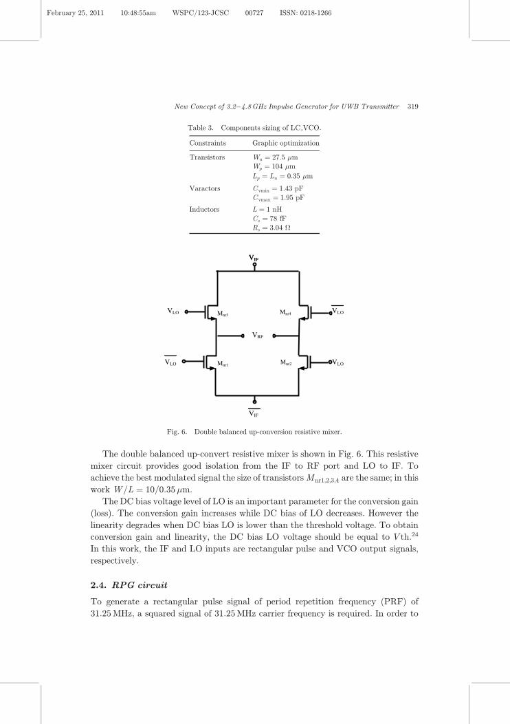
The double balanced up-convert resistive mixer is shown in Fig. 6. This resistive
mixer circuit provides good isolation from the IF to RF port and LO to IF. To
achieve the best modulated signal the size of transistorsM nr1;2;3;4 are the same; in this
work W=L ¼ 10=0:35�m.
The DC bias voltage level of LO is an important parameter for the conversion gain
(loss). The conversion gain increases while DC bias of LO decreases. However the
linearity degrades when DC bias LO is lower than the threshold voltage. To obtain
conversion gain and linearity, the DC bias LO voltage should be equal to V th.24
In this work, the IF and LO inputs are rectangular pulse and VCO output signals,
respectively.
2.4. RPG circuit
To generate a rectangular pulse signal of period repetition frequency (PRF) of
31.25MHz, a squared signal of 31.25MHz carrier frequency is required. In order to
Table 3. Components sizing of LC VCO.
Constraints Graphic optimization
Transistors Wn ¼ 27:5 �mWp ¼ 104 �m
Lp ¼ Ln ¼ 0:35 �m
Varactors C vmin ¼ 1:43 pF
C vmax ¼ 1:95 pF
Inductors L ¼ 1 nH
Cs ¼ 78 fF
Rs ¼ 3:04 �
VRF
Mnr3
VIF
VLO Mnr4
Mnr2Mnr1 VLO VLO
VLO
VIF
VIF
Fig. 6. Double balanced up-conversion resistive mixer.
New Concept of 3.2�4.8GHz Impulse Generator for UWB Transmitter 319
February 25, 2011 10:48:55am WSPC/123-JCSC 00727 ISSN: 0218-1266
minimize the number of blocks in an UWB generator architecture, it is essential to
obtain this signal from a LC VCO circuit. For this reason, a frequency divider circuit
block is required. The frequency of the output signal of LC VCO is 4GHz, so a divider
1/128 is required to get a signal of 31.25MHz. The RPG circuit consists of a frequency
divider, N-inverters, time delay and \AND" logic circuit (Fig. 3).
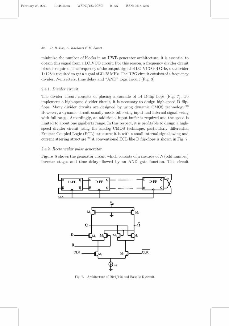
2.4.1. Divider circuit
The divider circuit consists of placing a cascade of 14 D-°ip °ops (Fig. 7). To
implement a high-speed divider circuit, it is necessary to design high-speed D °ip-
°ops. Many divider circuits are designed by using dynamic CMOS technology.28
However, a dynamic circuit usually needs full-swing input and internal signal swing
with full range. Accordingly, an additional input bu®er is required and the speed is
limited to about one gigahertz range. In this respect, it is pro¯table to design a high-
speed divider circuit using the analog CMOS technique, particularly di®erential
Emitter Coupled Logic (ECL) structure; it is with a small internal signal swing and
current steering structure.29 A conventional ECL like D °ip-°ops is shown in Fig. 7.
2.4.2. Rectangular pulse generator
Figure 8 shows the generator circuit which consists of a cascade of N (odd number)
inverter stages and time delay, °owed by an AND gate function. This circuit
CLK
D-FF D
Q
Q
D
D-FF D
Q
Q
D
D-FFD
Q
Q
D
Qout
IBS
Q
D
Vdd
D
Q
CLK CLK
M8
M6
M7
M5M3 M4
M1 M2
Fig. 7. Architecture of Div1/128 and Bascule D circuit.
320 D. B. Issa, A. Kachouri & M. Samet
February 25, 2011 10:48:55am WSPC/123-JCSC 00727 ISSN: 0218-1266
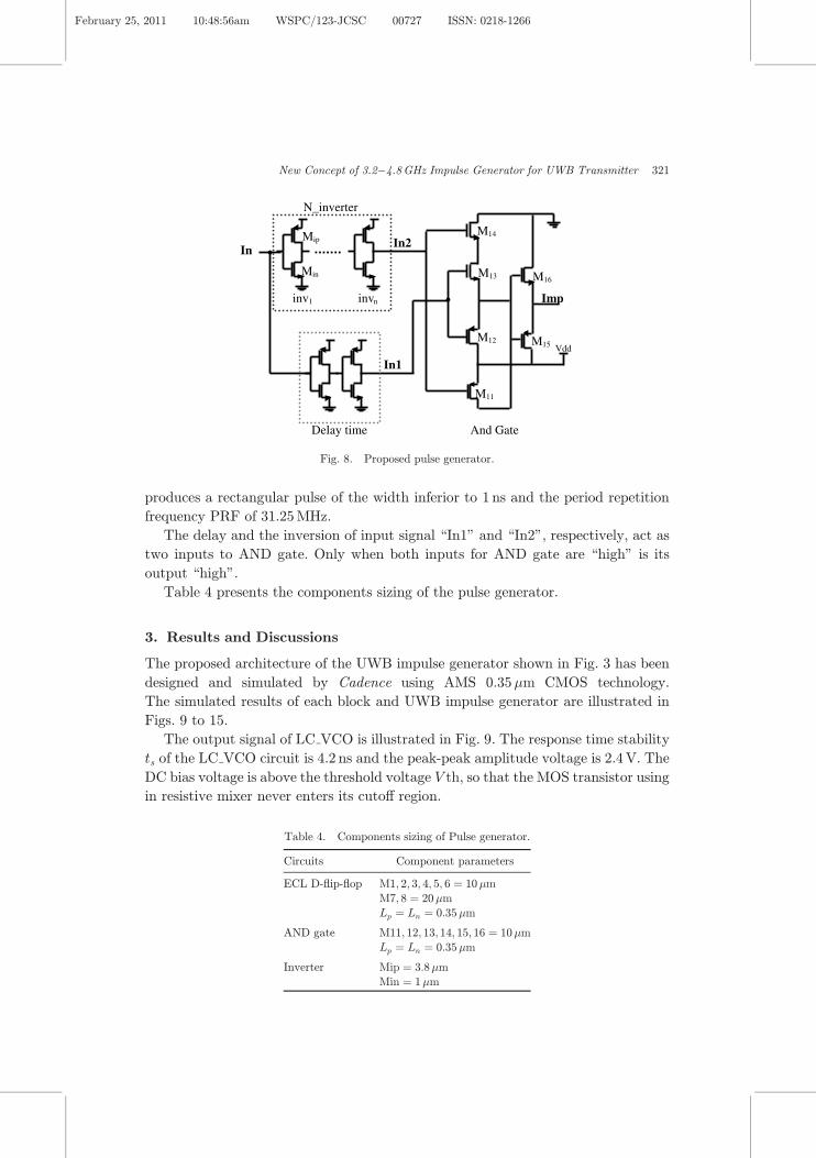
produces a rectangular pulse of the width inferior to 1 ns and the period repetition
frequency PRF of 31.25MHz.
The delay and the inversion of input signal \In1" and \In2", respectively, act as
two inputs to AND gate. Only when both inputs for AND gate are \high" is its
output \high".
Table 4 presents the components sizing of the pulse generator.
3. Results and Discussions
The proposed architecture of the UWB impulse generator shown in Fig. 3 has been
designed and simulated by Cadence using AMS 0:35�m CMOS technology.
The simulated results of each block and UWB impulse generator are illustrated in
Figs. 9 to 15.
The output signal of LC VCO is illustrated in Fig. 9. The response time stability
ts of the LC VCO circuit is 4.2 ns and the peak-peak amplitude voltage is 2.4V. The
DC bias voltage is above the threshold voltage V th, so that the MOS transistor using
in resistive mixer never enters its cuto® region.
M14
M13
M12
M11
M16
M15
And Gate Delay time
In In2
In1
inv1 invn
N_inverter
Imp
Vdd
Mip
Min
Fig. 8. Proposed pulse generator.
Table 4. Components sizing of Pulse generator.
Circuits Component parameters
ECL D-°ip-°op M1; 2; 3; 4; 5; 6 ¼ 10�m
M7; 8 ¼ 20�m
Lp ¼ Ln ¼ 0:35�m
AND gate M11; 12; 13; 14; 15; 16 ¼ 10�m
Lp ¼ Ln ¼ 0:35�m
Inverter Mip ¼ 3:8�m
Min ¼ 1�m
New Concept of 3.2�4.8GHz Impulse Generator for UWB Transmitter 321
February 25, 2011 10:48:56am WSPC/123-JCSC 00727 ISSN: 0218-1266
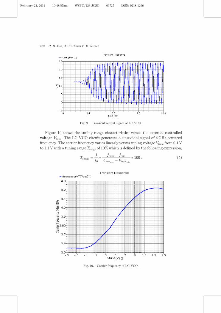
Figure 10 shows the tuning range characteristics versus the external controlled
voltage Vtune. The LC VCO circuit generates a sinusoidal signal of 4GHz centered
frequency. The carrier frequency varies linearly versus tuning voltage Vtune from 0.1V
to 1.1V with a tuning range Trange of 10%which is de¯ned by the following expression,
Trange ¼1
f 0� fmax � fmin
Vtunemax� Vtunemin
� 100 : ð5Þ
Fig. 9. Transient output signal of LC VCO.
Fig. 10. Carrier frequency of LC VCO.
322 D. B. Issa, A. Kachouri & M. Samet
February 25, 2011 10:48:57am WSPC/123-JCSC 00727 ISSN: 0218-1266
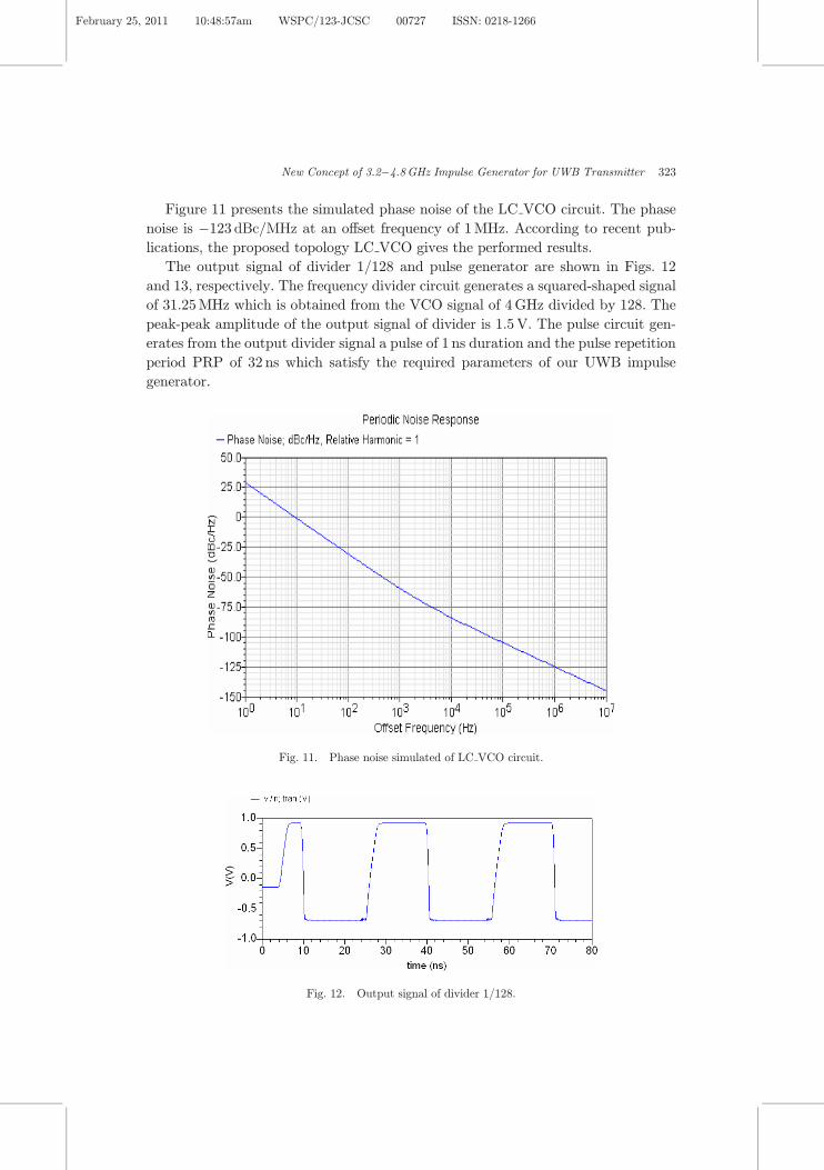
Figure 11 presents the simulated phase noise of the LC VCO circuit. The phase
noise is �123 dBc=MHz at an o®set frequency of 1MHz. According to recent pub-
lications, the proposed topology LC VCO gives the performed results.
The output signal of divider 1/128 and pulse generator are shown in Figs. 12
and 13, respectively. The frequency divider circuit generates a squared-shaped signal
of 31.25MHz which is obtained from the VCO signal of 4GHz divided by 128. The
peak-peak amplitude of the output signal of divider is 1.5V. The pulse circuit gen-
erates from the output divider signal a pulse of 1 ns duration and the pulse repetition
period PRP of 32 ns which satisfy the required parameters of our UWB impulse
generator.
Fig. 11. Phase noise simulated of LC VCO circuit.
Fig. 12. Output signal of divider 1/128.
New Concept of 3.2�4.8GHz Impulse Generator for UWB Transmitter 323
February 25, 2011 10:48:57am WSPC/123-JCSC 00727 ISSN: 0218-1266
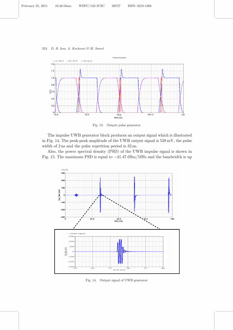
The impulse UWB generator block produces an output signal which is illustrated
in Fig. 14. The peak-peak amplitude of the UWB output signal is 528mV, the pulse
width of 2 ns and the pulse repetition period is 32 ns.
Also, the power spectral density (PSD) of the UWB impulse signal is shown in
Fig. 15. The maximum PSD is equal to �41:47 dBm=MHz and the bandwidth is up
Fig. 13. Output pulse generator.
Fig. 14. Output signal of UWB generator.
324 D. B. Issa, A. Kachouri & M. Samet
February 25, 2011 10:48:58am WSPC/123-JCSC 00727 ISSN: 0218-1266
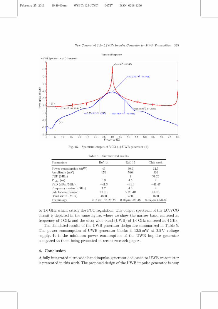
to 1.6GHz which satisfy the FCC regulation. The output spectrum of the LC VCO
circuit is depicted in the same ¯gure, where we show the narrow band centered at
frequency of 4GHz and the ultra wide band (UWB) of 1.6GHz centered at 4GHz.
The simulated results of the UWB generator design are summarized in Table 5.
The power consumption of UWB generator blocks is 12.5mW at 2.5V voltage
supply. It is the minimum power consumption of the UWB impulse generator
compared to them being presented in recent research papers.
4. Conclusion
A fully integrated ultra wide band impulse generator dedicated to UWB transmitter
is presented in this work. The proposed design of the UWB impulse generator is easy
Table 5. Summarized results.
Parameters Ref. 14 Ref. 15 This work
Power consumption (mW) 45 30.6 12.5
Amplitude (mV) 170 540 500PRF (MHz) − 1 31.25
Ppulse (ns) 0.3 4.5 2
PSD (dBm/MHz) �41:3 �41:3 �41:47
Frequency centred (GHz) 7.7 4.3 4
Side lobe-supression 20 dB > 20 dB 20 dBBand width (MHz) 4800 460 1600
Technology 0:18�m BiCMOS 0:18�m CMOS 0:35�m CMOS
Fig. 15. Spectrum output of VCO (1) UWB generator (2).
New Concept of 3.2�4.8GHz Impulse Generator for UWB Transmitter 325
February 25, 2011 10:49:00am WSPC/123-JCSC 00727 ISSN: 0218-1266
to integrate which is composed of the LC voltage controlled oscillator, rectangular
pulse generator and mixer circuit. This generator has been designed to employ in the
band width of 1.6 GHz (3.2�4.8GHz) at a centered frequency of 4GHz. The design is
implemented in Cadence using CMOS 0:35�m AMS process technology. The
simulated results prove the performance of this generator which has produced a
UWB impulse signal centered at a frequency of 4GHz, the frequency bandwidth of
1.6GHz and the Power Spectral Density (PSD) is limited to �41:47 dBm=MHz. The
pulse width of output signal is 2 ns and the period repetition pulse is 32 ns. The total
power consumption of this circuit is about 12.5mW at 2.5V power supply.
This UWB impulse generator architecture is intended with fully integrated, low
power consumption, low complexity and is in agreement with the FCC regulation. In
future works we will develop this topology to multi-bands UWB generator.
Acknowledgment
The authors would like to thank Prof. Mohamed Masmoudi for his help, and for the
designed assistance by Cadence in the EMC laboratory, ENIS, Tunisia.
References
1. S. Roy, J. R. Foerster, S. Somayazulu and D. G. Leeper, Ultrawideband radio design: Thepromise of high-speed, shortrange wireless connectivity, Proc. IEEE 92 (2004) 295�310.
2. R. Fleming, C. Kushner, G. Roberts and U. Nandiwada, Rapidacquisition for ultra-wideband localizers, IEEE Conf. Ultra Wideband Systems Technology, Baltimore,Maryland, USA (2002), pp. 245�249.
3. P. P. Mercier, D. C. Daly and A. P. Chandrakasan, A 19pJ/pulse UWB transmitter withdual capacitively-coupled digital power ampli¯ers, IEEE Radio Frequency IntegratedCircuits Symp. (2008), pp. 47�50.
4. M. Abtahi, M. Mirsha¯ei, J. Magn�e, L. A. Rusch and S. LaRochelle, Generation of power-e±cient FCC-compliant UWB waveforms using FBGs: Analysis and experiment,J. Lightwave Technol. 26 (2008) 628�635.
5. M. Abtahi, M. Mirsha¯ei, J. Magn�e, L. A. Rusch and S. LaRochelle, Ultra-widebandwaveform generator based on optical pulse-shaping and FBG tuning, IEEE PhotonicsTechnol. Lett. 20 (2008) 135�137.
6. R. Hou, N. Saputra and J. R. Long, Super-regenerative receiver for UWB-FM, Proc. 19thAnn. Workshop on Circuits, Systems and Signal Processing (ProRisc), Veldhoven, STW(2008), pp. 179�183.
7. Y. Wang, A. M. Niknejad, V. Gaudet and K. Iniewski, A CMOS IR-UWB transceiverdesign for contact-less chip testing applications, IEEE Trans. Circuits Syst. 55 (2008)334�338.
8. Q. Wang and J. Yao, An electrically switchable optical ultrawideband pulse generator,J. Lightwave Technol. 25 (2007) 3626�3633.
9. M. Ch. Ha, Y. Park and Y. S. Eo, A 3�5GHz non-coherent IR-UWB receiver,J. Semicond. Technol. Sci. 8 (2008) 279�282.
10. L. Weinan, H. Yumei and H. Zhiliang, A low power 3�5 GHz CMOS UWB receiver front-end, J. Semicond. 30 (2009) 1381�1383.
326 D. B. Issa, A. Kachouri & M. Samet
February 25, 2011 10:49:02am WSPC/123-JCSC 00727 ISSN: 0218-1266
11. FCC, First report and order, revision of the part 15 commission's rules regarding ultra-wideband transmission systems, ET Docket 98�153 (2002).
12. P. Protiva, J. Mrkvica and J. Machac, Universal generator of ultra-wideband pulses,Radioengineering 17 (2008) 74�78.
13. A. Ousliman, G. Vernet, H. Hardallah and R. Adder, Large amplitude picosecond stepgeneration with FETs, Electron. Lett. 26 (1990) 1563�1564.
14. X. Fan, G. Fischer and B. Dietrich, An integrated 3.1�5.1GHz pulse generator for ultra-wideband wireless localization systems, Advanced Radio Science (2006), pp. 247�250.
15. S. Bagga, A. V. Vorobyov, S. A. P. Haddad, A. G. Yarovoy, W. A. Serdijn and J. R.Long, Codesign of a pulse generator and miniaturized antennas for IR-UWB, IEEETrans. Microw. Theor. Tech. 54 (2006) 1656�1666.
16. C. Shu, M. S. Kang, S. K. Han and S. G. Lee, A single chip CMOS transmitter for UWBpulse radar applications, Microwave Conf. APMC, Asia-Paci¯c (2008).
17. E. Kougianos and S. P. Mohanty, Impact of gate-oxide tunneling on mixed-signal designand simulation of a nano-CMOS VCO, Microelectron. J. 40 (2009) 95�103.
18. S. M. Oh, C. Kim and S. Lee, A 74%, 1.56�2.71GHz, wide-tunable LC-tuned VCO in0.35-�m CMOS technology, Microwave and Optical Technology Letters (2003), pp.98�100.
19. A. Kachouri, D. Ben Issa, N. Boughanmi and M. Samet, A new temperature compen-sation method for a 2.5GHz integrated VCO, Int. J. Comput. Sci. Network Security7 (2007) 78�85.
20. D. Ben Issa, A. Kachouri and M. Samet, Graphical optimization of 4 GHz LC oscillator,Int. Conf. Design & Technology of Integrated Systems (2009).
21. C. P. Yue and S. S. Wong, Physical modeling of spiral inductors on silicon, IEEE Trans.Electron Dev. 47 (2000) 560�568.
22. H. Jiang, Y. Wang, J. L. A. Yeh and N. C. Tien, On-chip spiral inductors suspended overdeep copper-lined cavities, IEEE Trans. Microw. Theor. Tech. 48 (2000) 2415�2423.
23. F. Ellinger et al., 30�40-GHz drain-pumped passive-mixer MMIC fabricated on VLSISOI CMOS technology, IEEE Trans. Microw. Theor. Tech. 52 (2004) 1382�1391.
24. J. Zhao, Silicon-based RFIC multi-band transmitter front ends for ultra-widebandcommunications and sensor applications, Ph.D. thesis, Faculty of the Virginia Poly-technic Institute and State University (2007).
25. S. Douss, F. Touati and M. Loulou, Design optimization methodology of CMOS activemixers for multi-standard receivers, Int. J. Electron. Circuits Syst. 1 (2007) 1�9.
26. C. Huang and W. Chen, Multi-band/multi-mode current folded up-convert mixer design,Proc. Asia-Paci¯c Microwave Conference IEICE (2006).
27. S. G. Lee and J.-K. Choi, Current-reuse bleeding mixer, Electron. Lett. 36 (2000)696�697.
28. M. W. Hwang, J. T. Hwang and G. H. Cho, Design of high speed CMOS prescaler, IEEEAsia Paci¯c Conf. ASICs (2000), pp. 87�90.
29. N. Foroudi and T. A. Kwasniewski, CMOS high-speed dual-modulus frequency divider forRF frequency synthesis, IEEE J. Solid-State Circuits 30 (1995) 93�100.
New Concept of 3.2�4.8GHz Impulse Generator for UWB Transmitter 327
February 25, 2011 10:49:02am WSPC/123-JCSC 00727 ISSN: 0218-1266