Modeling Low-k DielectricBreakdown to DetermineLifetime RequirementsMuhammad Bashir and Linda Milor
Georgia Institute of Technology
�HISTORICALLY, THE MAJOR CAUSE of interconnect
wearout has been electromigration. Recently, be-
cause of the introduction of new materials (copper,
low-k dielectrics), the increase in the number of inter-
connect layers with smaller geometries and higher
current densities, and the concomitant increase in
on-chip temperatures, low-k dielectric breakdown
and stress migration have emerged as new sources
of interconnect wearout. This article focuses on mod-
eling one of these new wearout mechanisms: low-k
dielectric breakdown.
In the past, the lifetime of the dielectric between
interconnect lines has not been a concern, because
of the dielectric’s thickness. However, in recent
years copper and low-k interconnect systems have
become vulnerable to breakdown because of the
lower breakdown field strengths of porous low-k
materials, the susceptibility of low-k materials to
mechanical damage by chemical mechanical pol-
ishing (CMP), and the high susceptibility of low-k
materials to copper drift. These problems are com-
pounded because the supply voltage is not scaled
as aggressively as feature size, which results in
exponentially escalating electric fields among inter-
connects in each technology generation. Porosity
degrades the electrical and structural properties
of copper and low-k systems further, because of,
for example, the absorption of chemi-
cals through pores that have an open
connection to the surface.
Back-end dielectrics differ from thin
gate oxides in several ways. First, unlike
the gate oxide, the back-end dielectric
undergoes many process steps that
can potentially damage the interfaces,
which can become trap sites and assist in conduc-
tion. Second, the quality of the back-end dielectric,
which is deposited rather than thermally grown, is
far poorer, resulting in higher defect densities. Third,
back-end geometries in chips have a wide variety of
geometries that might impact chip lifetime. The ap-
propriate features to extract from a chip and the fail-
ure rates to measure from test structures are not
known. As a result, time-dependent dielectric break-
down (TDDB) of damascene structures must be
assessed as a system consisting of a dielectric, diffu-
sion barrier, cap layer (SiC, for example), and copper
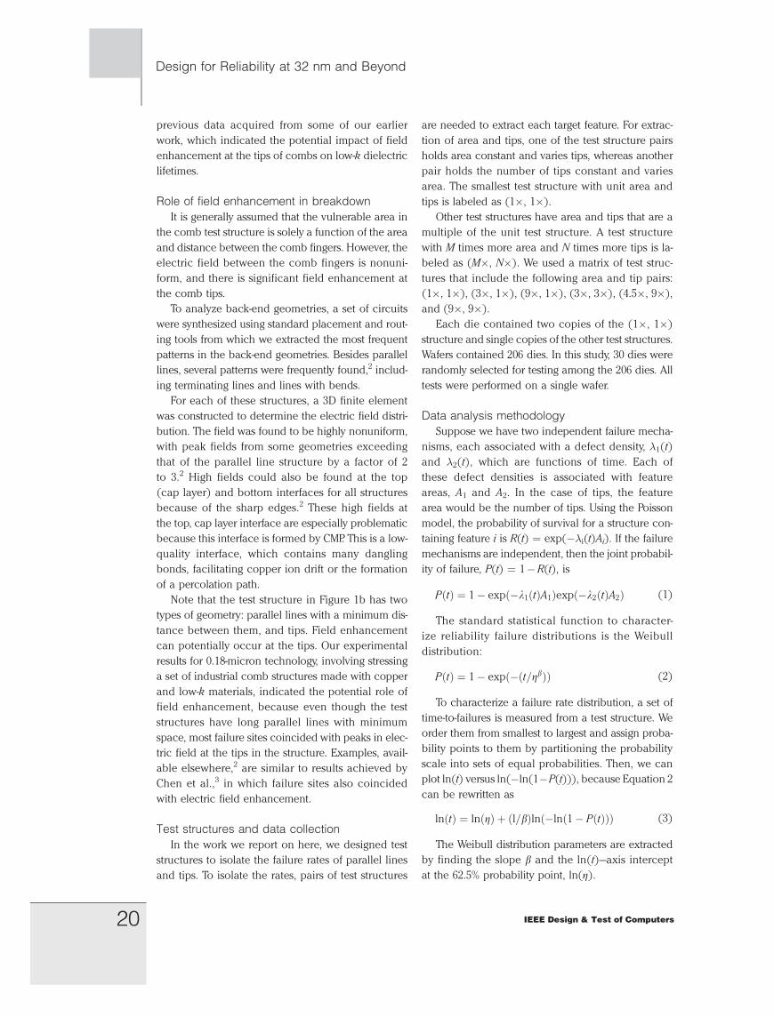
interconnect. Figure 1a shows an example of this
system.
In this article, we explore how interconnect geom-
etry impacts failure rates and describe our failure-rate
models for determining the time-to-fail at small per-
centiles (the tails of the distribution) while account-
ing for the observed curvature in Weibull plots. We
use the data we obtained from back-end dielectric
breakdown lifetime measurements directly to deter-
mine the impact of line width variation. We also dis-
cuss how we use this information to determine
equivalent lifetime requirements that consider both
the impact of die-to-die line width variation and the
traditional failure rate distribution, modeled by Wei-
bull statistics.
Design for Reliability at 32 nm and Beyond
Editor’s note:
Low-k dielectric breakdown and stress migration have emerged as new
sources of wearout for on-chip interconnect. This article analyzes statistical
data from a 45-nm test chip and constructs a methodology to determine the
lifetime of low-k materials under process variations.
��Yu Cao, Arizona State University
0740-7475/09/$26.00 �c 2009 IEEE Copublished by the IEEE CS and the IEEE CASS IEEE Design & Test of Computers18

Back-end dielectric reliabilityBack-end dielectric reliability is measured with
comb test structures, as illustrated in Figure 1b. The
comb structures create a lateral stress across the dielec-
tric between the comb fingers, which are separated by
the minimum-space design rule. A voltage difference is
applied to the comb, creating a lateral electric field
through the intralayer dielectric. The current between
the comb fingers is monitored, and breakdown is
observed when the current exceeds a fixed threshold.
In collecting data for a sample of comb structures,
we order the data from shortest to longest breakdown
time. We assign each time point a probability point, P,
by partitioning the probability scale equally. Figure 2
shows an example.
The data is fit by a distribution, either the Weibull
or the lognormal distribution, in order to enable
extrapolations to lifetimes at low percentiles. Let’s
consider the Weibull distribution, as an example.
When constructing a model by fitting a Weibull distri-
bution to a dataset, two parameters are extracted: the
characteristic lifetime (62.5% probability point) Z and
the shape parameter b. The intercept of the x-axis is Z,
and the slope of the curve is b. The resulting data is
then scaled to use conditions and to the vulnerable
area corresponding to the chip.
When considering layout geometries, we note that
field enhancement occurs at the tips of the comb
structures. Prior work has indicated that failure sites
correspond with locations where there is field en-
hancement.2,3 To address this concern, we have
designed a set of test structures that can separate
the impact of field enhancement at the comb tips.
Analysis of data from these test structures has
required developing a methodology to determine fail-
ure rates for structures containing multiple feature
geometries��that is, parallel lines and tips.
The result of data analysis is the construction of an
accurate model to determine failure rates at low per-
centiles. As Figure 2 shows, the data points do not fall
on a straight line, as expected for Weibull statistics.
Chen et al. noted that line width variation can be
as large as �30%.4 This variation distorts the Weibull
curves used to determine a structure’s lifetime. As a
result, direct extraction of parameters Z and bwould be inaccurate.
Die-to-die line width variation can be eliminated
during Weibull parameter extraction through calibra-
tion of lifetime measurements based on capacitance
measurements, which can be used to compute the
mean distance between the lines of the comb struc-
ture.4 However, because of the structure’s complexity,
capacitance is also affected by variation in the low-k
dielectric constant as a function of the stack’s compo-
sition, and variation in the dielectric constant is con-
sequently confounded with variation in line space.
Hence, capacitance measurements overestimate
line width variation.
Impact of field enhancementTo determine the impact of field enhancement, we
conducted several experiments. Here, we discuss
(a) (b)
BarrierTEOS
SiC
Cu Cu
SiONPSG
SiC
Dielectric Dielectric
Figure 1. Cross-section of an example copper and low-k
interconnect system, including the barrier layer and cap
layer (a), and comb test structure used to measure back-end
dielectric breakdown (b).
–6
–5
–4
–3
–2
–1
0
1
2
3
4 6 8 10 12
ln(time) [a.u.]
ln(–
ln(1
–P))
1X 3X 4.5X 9X
Figure 2. Example Weibull plot of ln(2ln(1 2 P)) vs.
ln(time-to-failure(i)) for comb test structures with four
areas: 13, 33, 4.53, and 93. (Source: Bashir and Milor.1)
19November/December 2009
previous data acquired from some of our earlier
work, which indicated the potential impact of field
enhancement at the tips of combs on low-k dielectric
lifetimes.
Role of field enhancement in breakdown
It is generally assumed that the vulnerable area in
the comb test structure is solely a function of the area
and distance between the comb fingers. However, the
electric field between the comb fingers is nonuni-
form, and there is significant field enhancement at
the comb tips.
To analyze back-end geometries, a set of circuits
were synthesized using standard placement and rout-
ing tools from which we extracted the most frequent
patterns in the back-end geometries. Besides parallel
lines, several patterns were frequently found,2 includ-
ing terminating lines and lines with bends.
For each of these structures, a 3D finite element
was constructed to determine the electric field distri-
bution. The field was found to be highly nonuniform,
with peak fields from some geometries exceeding
that of the parallel line structure by a factor of 2
to 3.2 High fields could also be found at the top
(cap layer) and bottom interfaces for all structures
because of the sharp edges.2 These high fields at
the top, cap layer interface are especially problematic
because this interface is formed by CMP. This is a low-
quality interface, which contains many dangling
bonds, facilitating copper ion drift or the formation
of a percolation path.
Note that the test structure in Figure 1b has two
types of geometry: parallel lines with a minimum dis-
tance between them, and tips. Field enhancement
can potentially occur at the tips. Our experimental
results for 0.18-micron technology, involving stressing
a set of industrial comb structures made with copper
and low-k materials, indicated the potential role of
field enhancement, because even though the test
structures have long parallel lines with minimum
space, most failure sites coincided with peaks in elec-
tric field at the tips in the structure. Examples, avail-
able elsewhere,2 are similar to results achieved by
Chen et al.,3 in which failure sites also coincided
with electric field enhancement.
Test structures and data collection
In the work we report on here, we designed test
structures to isolate the failure rates of parallel lines
and tips. To isolate the rates, pairs of test structures
are needed to extract each target feature. For extrac-
tion of area and tips, one of the test structure pairs
holds area constant and varies tips, whereas another
pair holds the number of tips constant and varies
area. The smallest test structure with unit area and
tips is labeled as (1�, 1�).
Other test structures have area and tips that are a
multiple of the unit test structure. A test structure
with M times more area and N times more tips is la-
beled as (M�, N�). We used a matrix of test struc-
tures that include the following area and tip pairs:
(1�, 1�), (3�, 1�), (9�, 1�), (3�, 3�), (4.5�, 9�),
and (9�, 9�).
Each die contained two copies of the (1�, 1�)
structure and single copies of the other test structures.
Wafers contained 206 dies. In this study, 30 dies were
randomly selected for testing among the 206 dies. All
tests were performed on a single wafer.
Data analysis methodology
Suppose we have two independent failure mecha-
nisms, each associated with a defect density, �1(t)
and �2(t), which are functions of time. Each of
these defect densities is associated with feature
areas, A1 and A2. In the case of tips, the feature
area would be the number of tips. Using the Poisson
model, the probability of survival for a structure con-
taining feature i is R(t) ¼ exp(��i(t)Ai). If the failure
mechanisms are independent, then the joint probabil-
ity of failure, P(t) ¼ 1�R(t), is
PðtÞ ¼ 1� expð�l1ðtÞA1Þexpð�l2ðtÞA2Þ (1)
The standard statistical function to character-
ize reliability failure distributions is the Weibull
distribution:
PðtÞ ¼ 1� expð�ðt=hbÞÞ (2)
To characterize a failure rate distribution, a set of
time-to-failures is measured from a test structure. We
order them from smallest to largest and assign proba-
bility points to them by partitioning the probability
scale into sets of equal probabilities. Then, we can
plot ln(t) versus ln(�ln(1�P(t))), because Equation 2
can be rewritten as
lnðtÞ ¼ lnðhÞ þ ðl=bÞlnð�lnð1� PðtÞÞÞ (3)
The Weibull distribution parameters are extracted
by finding the slope b and the ln(t)�axis intercept
at the 62.5% probability point, ln(Z).
Design for Reliability at 32 nm and Beyond
20 IEEE Design & Test of Computers

If we have multiple failure mechanisms, then by
rearranging Equation 1 we have
lnð�lnð1� PðtÞÞÞ ¼X
i
liðtÞAi
!(4)
Hence, we can see that the Weibull distribution
plot also gives an indication of the probability distri-
bution function for the number of defects at break-
down, �iAi.
Suppose two test structures contain all the same
features, except that in one structure there is 3� of
a target feature (area) versus 1� in the other struc-
ture. The difference between these two structures is
2� area. The number of defects in the 2� area is
l2�ðtÞA2� ¼ l3�ðtÞA3� � l1�ðtÞA1� (5)
We can, therefore, extract values for �2�(t)A2�
using the Weibull distribution plots for the 3� and
1� test structures. Using Equation 4, at any time t*,
we have
lnð�lnð1� P2�ðt�ÞÞÞ ¼ lnðlnð1� P1�ðt�ÞÞ� lnð1� P3�ðt�ÞÞÞ (6)
where the values for P1�(t*) and P3�(t*) are known
from measured data from the 1� and 3� test
structures. From Equation 6, we solve for P2�(t*).
Impact of field enhancement at tips
The test structures with 1� tips were used to ex-
tract the failure rate due to parallel lines with the min-
imum distance between the lines. The analysis
methodology subtracted the impact of 1� tips from
the measured results for these test structures, in accor-
dance with Equation 6.
The measurement data related to area indicated a
strong impact of area. We synthesized data sets for 2�of the target feature (area) and no tips using 1� and
3� test structures, for 6� area and no tips using 9�and 3� test structures, and for 8� area and no tips
using 9� and 1� test structures.
The data sets were merged so that they all corre-
sponded to 1� area. This was done with a transforma-
tion of the probability scale before extracting the
model,5,6 by plotting ln(�ln(1� P(t))/N) versus
ln(t), where N ¼ 2, N ¼ 6, and N ¼ 8, for the 2�,
6�, and 8� area data sets, respectively. This transfor-
mation of the probability scale is based on the Pois-
son model, which can show that if a test structure
has an area that is N times larger, the corresponding
plot for the larger area structure is the following:
lnðtÞ ¼ ln hþ 1
bln � 1
Nlnð1� PðtÞÞ
� �(7)
When the data sets are merged, the resulting distri-
butions fall on a straight line, as Figure 3 shows. We
denote the extracted model with the Weibull charac-
teristic lifetime Z* and the Weibull shape parameter
b*, to get the equation for 1� area:
lnðtÞ ¼ lnðh�Þ þ ð1=b�Þlnð�lnð1�PðtÞÞÞ (8)
The data on tips is inconclusive. A comparison of
the 3� area structures (which vary the number of
tips) indicated an impact of tips, whereas a compari-
son of the 9� area structures (which also vary the
number of tips) showed no impact of tips. The com-
plete data set must be considered to determine the
impact of tips.
We use the model in Equation 8 to synthesize data
sets that correspond to 9� area with varying numbers
of tips. To do this, we add defect densities corre-
sponding to the appropriate area correction. In
other words, for the 1� model, we add defect den-
sities corresponding to 8� area. If Z* and b* are
the parameters corresponding to the 1� area
model, and if P(ti) is the probability point corre-
sponding to breakdown time ti, then the probability
–6
–5
–4
–3
–2
–1
0
1
2
4 6 8 10 12ln(time) [a.u.]
ln(–
ln(1
–P))
2X 6X 8X Model
Figure 3. Merged data set for 23, 63, and 83 area, with the
probability scale modified to correspond to 13 area. The plots
are for In(Sili(t)Ai), but labeled as ln(2ln(12P)), because they
are equivalent, according to Equation 4. (Source: Bashir and
Milor.1)
21November/December 2009
point P0(ti), corresponding to 9� area at breakdown
time ti, is
lnð�lnð1� P 0ðtiÞÞÞ ¼ lnð�lnð1� PðtiÞÞþ 8ðexpðb�ðlnðtiÞ � lnðh�ÞÞÞÞÞ (9)
The number of defects at failure for 8� area is
8(exp(b*(ln(ti) � ln(Z*)))). Similarly, for 4.5� area,
we add defects corresponding to 4.5� area. The syn-
thesized Weibull curves obtained after converting all
data sets to 9� area show no impact of tips. Variation
among data sets appears to be random.
Failure rate modelingHere, we discuss our results in modeling the fail-
ure rate in the presence of die-to-die line width varia-
tion. We first extracted the Weibull shape parameter
via area scaling, and then we extracted the impact
of die-to-die line width variation via the slope of the
Weibull curve.
Extracting the Weibull shape parameter
In this study, we’ve used test structures with four
areas: 1�, 3�, 4.5�, and 9�, implemented with
45-nm technology. For this set of test structures,
the distance between the lines of the comb,
which determines the applied electric field through
the dielectric, is fixed. In addition, we’ve also used
a test structure with a smaller distance between the
lines with 1� area.
Figure 2 shows the data for the four different areas.
Unlike what is assumed with the Weibull distribution
model, the failure rate distributions aren’t linear.
Through simulations, we observed that random varia-
tion in line width creates curvature in the failure rate
distributions. It also degrades the measured Weibull
shape parameter b, although the characteristic life-
time (x-intercept) is less affected. Modeling required
that we determine the Weibull shape parameter
in the absence of line width variation.
The standard approach to determine the charac-
teristic lifetime Z and the Weibull shape parameter
b is to transform the probability scales of all of the
data sets by plotting ln(�ln(1�P(t))/N) versus
ln(t), where N is the area ratio, and then to fit a
straight line to the data by regression, as Figure 4a
shows. However, curvature could lead to erroneous
extraction of the Weibull parameters. The extracted
Weibull parameters are used to find the lifetime at
a low probability point, such as the 0.0001 point.
This is well beyond the data points in the data
set, since ln(�ln(1� 0.0001))¼�9.21, as Figure 4a
shows.
Errors in the extraction of slope can create sig-
nificant errors in the estimated lifetime at low prob-
abilities. Consider a data set with a true Weibull
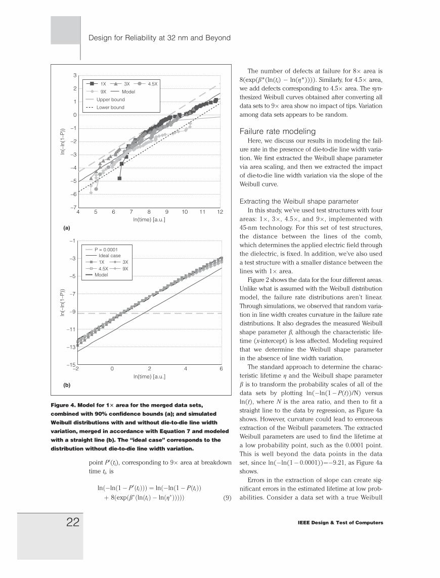
(a)
(b)
–7
–6
–5
–4
–3
–2
–1
0
1
2
3
4 5 6 7 8 9 10 1211ln(time) [a.u.]
ln(–
ln(1
–P))
1X 3X 4.5X
9X Model
Upper bound
Lower bound
–15
–13
–11
–9
–7
–5
–3
–1
–2 0 2 4 6ln(time) [a.u.]
ln(–
ln(1
–P))
P = 0.0001Ideal case1X 3X4.5X 9X
Model
Figure 4. Model for 13 area for the merged data sets,
combined with 90% confidence bounds (a); and simulated
Weibull distributions with and without die-to-die line width
variation, merged in accordance with Equation 7 and modeled
with a straight line (b). The ‘‘ideal case’’ corresponds to the
distribution without die-to-die line width variation.
Design for Reliability at 32 nm and Beyond
22 IEEE Design & Test of Computers
distribution. If we introduce variation in the die-to-
die line width with a standard deviation of 10%
and merge the data sets via Equation 7, we achieve
the result shown in Figure 4b, together with the
extracted model. Die-to-die line width variation cre-
ates at least an order of magnitude of error in the
expected lifetime at the 0.0001 probability point.
Instead, as in the research reported by Chen et al.,4
we use the area-scaling formula to extract the Weibull
shape parameter. The relationship between character-
istic lifetimes for structures with different areas is
given by
lnðhN�Þ ¼ lnðh1�Þ þ ð1=bÞlnðA1�=AN�Þ (10)
where ZN� and Z1� are characteristic lifetimes for the
N� and 1� area test structures, and AN�/A1� ¼ N is
the area ratio between the structures.
To extract the characteristic lifetime, we fit a qua-
dratic model to each data set to find the x-intercept.
Fitting a regression line to the characteristic lifetime
data points determines the Weibull shape parameter
b, with less degradation due to die-to-die line width
variation. However, the extracted models do not
match well with the original data, because of die-to-
die line width variation.
Extracting die-to-die line width variation
The impact of random die-to-die line width varia-
tion is to degrade the slope of the Weibull curves.
We can therefore determine die-to-die line width vari-
ation by extracting the difference in slope between band the data.
The slope depends on die-to-die variation and
whether we assume an E model7,8 or affiffiffiEp
model,9-11
where E is the electric field between the lines. The elec-
tric field is a function of line spacing. To determine the
impact of line spacing on electric field, we use the data
set with a different distance between the lines. With the
E model,
lnðhÞ ¼ a1 �b1
s(11)
where s is the distance between the lines, and a1
and b1 are arbitrary fitting constants. With theffiffiffiEp
model,
lnðhÞ ¼ a2 �b2ffiffiffi
sp (12)
where a2 and b2 are arbitrary fitting constants. With
two values for s, we determine values of the
constants. If we were to plot the relationship
between the characteristic lifetime and distance be-
tween the lines, these models would be indistinguish-
able for the range of data available from the two test
structures.
In this analysis, we’ve assumed normally distrib-
uted die-to-die line width variation and optimized
the fit between the data and the model, given the
value of b as we determined earlier, to find the stan-
dard deviation of die-to-die variation. Figure 5a shows
the results for theffiffiffiEp
model. Note that the models re-
semble the data sets. The result for the E model is
similar.
Figure 5b shows the confidence bounds for the 1�model. As we can see, the confidence bounds are
similar in size to those in Figure 4a. The variation is
dominated by accuracy in extraction of the Weibull
parameters with Equation 10. We also found that
the best fit model was essentially independent of
using either the E orffiffiffiEp
models.
In fitting the models in Equations 11 and 12, we
must consider any print bias, because the drawn
distance between the lines in the layout might not
match the printed distance exactly. Print bias is
the difference between the distance between the
lines in the layout and those in silicon. The manu-
facturer selects it to minimize interconnect delays.
For our test structures, we didn’t know the exact
values for print bias. So, we considered several val-
ues of print bias and found that for each value of
bias the optimum fit resulted in the same value
for the standard deviation for the distance between
the lines.
Lifetime and probability pointsThe traditional approach to determine lifetime for
a test structure (after area scaling and projection to
use conditions) for a fixed probability point, such
as 0.0001, involves analyzing lifetime at a single
value of distance between the lines. For example,
for the probability of 0.0001, which corresponds to
�9.21 on the Weibull scale, we simply find the life-
time that corresponds to this probability point. This
method involves solving a 1D problem and is illus-
trated in Figure 4b.
The introduction of random die-to-die line width
variation impacts determination of the expected life-
time at the target probability point. Random die-to-
die line width variation introduces a second dimen-
sion into the problem, because there are now two
23November/December 2009

simultaneous mechanisms that can degrade life-
time. Specifically, if we consider variation in line
width, the characteristic lifetime varies in accor-
dance with Equations 11 and 12. Figure 6a illustrates
probability versus distance between the lines for
several fixed values of lifetime. We can see that
the probability of having a lifetime worse than a
fixed value increases drastically as the distance be-
tween the lines decreases.
When the distance between lines varies, the prob-
ability of having a lifetime worse than a specified
value involves integrating the probabilities in
Figure 6a over the distribution of values of distance
between the lines. For a normal distribution of dis-
tance, the integral is a function of the variation’s stan-
dard deviation. Figure 6b shows the impact of
variation on lifetime. Clearly, when line width varia-
tion approaches a standard deviation of 10%, life-
times improved by more than an order of
magnitude are required to achieve the same probabil-
ity of failure. In addition, the results are almost insen-
sitive to the choice of model, E orffiffiffiEp
at test
conditions; however, the choice of model does im-
pact the projection to use conditions. Note that the
expected lifetime depends on two parameters: print
bias and random die-to-die variation in distance.
Extracted die-to-die variation in distance between
the lines was found to be insensitive to bias. However,
lifetime projections at small percentiles are sensitive
to print bias. Hence, it’s important to verify print
bias with additional data prior to making lifetime
projections.
THIS RESEARCH has looked at some interconnect geo-
metries to determine their potential impact on failure
rates. Although no significant impact was found to
have resulted from field enhancement at the comb
tips, future work will look into a larger set of geomet-
ric features, such as line width, vias, and bends, to im-
prove our understanding of the role of interconnect
geometry on time-to-failure.
Failure rates vary both as a function of Weibull sta-
tistics and as a function of die-to-die line width varia-
tion. Determination of whether or not a process
satisfies a lifetime requirement should take into ac-
count both factors. As variation becomes large, the
lifetimes that achieve the same target probability of
failure are orders of magnitude lower than without
die-to-die line width variation. �
AcknowledgmentsWe thank the Semiconductor Research Corpora-
tion for financial support, under task 1376.001, and
Design for Reliability at 32 nm and Beyond
(a)
(b)
–6
–5
–4
–3
–2
–1
0
1
2
3
4 6 8 10 12ln(time) [a.u.]
ln(–
ln(1
–P))
1X 3X4.5X 9X1X Model3X Model4.5X Model9X Model
–7
–6
–5
–4
–3
–2
–1
0
1
2
3
4 5 6 7 8 9 10 11 12
ln(time) [a.u.]
ln(–
ln(1
–P))
Data Model
Upper bound
Lower bound
Figure 5. Models for the data sets using the area-scaling
formula and adding die-to-die variation with theffiffiffiffiEp
model (a),
and the extracted model for the 13 data set and the 90%
confidence bounds (b). (Source: Bashir and Milor.1)
24 IEEE Design & Test of Computers

AMD for providing the wafers used to collect the data
in this study. We also thank Changsoo Hong and Soh-
rab Aftabjahani for designing and laying out the test
structures.
�References1. Reprinted from Microelectronics Reliability, vol. 49,
nos. 9-11, M. Bashir and L. Milor, ‘‘A Methodology to
Extract Failure Rates for Low-k Dielectric Breakdown
with Multiple Geometries and in the Presence of Die-to-
Die Linewidth Variation,’’ pp. 1096-1102, �c 2009, with
permission from Elsevier.
2. C. Hong, L. Milor, and M.Z. Lin, ‘‘Analysis of the Layout
Impact on Electric Fields in Interconnect Structures Using
Finite Element Method,’’ Microelectronics and Reliability,
vol. 44, Sept.�Nov. 2004, pp. 1867-1871.
3. F. Chen et al., ‘‘Reliability Characterization of BEOL Ver-
tical Natural Capacitor Using Copper and Low-k SiCOH
Dielectric for 65nm RF and Mixed-Signal Applications,’’
Proc. IEEE Int’l Reliability Physics Symp., IEEE Press,
2006, pp. 490-495.
4. F. Chen et al., ‘‘The Effect of Metal Area and Line Spac-
ing on TDDB Characteristics of 45nm Low-k SiCOH
Dielectrics,’’ Proc. IEEE Int’l Reliability Physics Symp.,
IEEE Press, 2007, pp. 382-389.
5. E.Y. Wu and R.P. Vollertsen, ‘‘On the Weibull Shape
Factor of Intrinsic Breakdown of Dielectric Films and
Its Accurate Experimental Determination��Part 1:
Theory, Methodology, Experimental Techniques,’’
IEEE Trans. Electron Devices, vol. 49, no. 12, 2002,
pp. 2131-2140.
6. E.Y. Wu et al., ‘‘Challenges for Accurate Reliability
Projections in the Ultra-thin Oxide Regime,’’ Proc. IEEE
Int’l Reliability Physics Symp., IEEE Press, 1999,
pp. 57-65.
7. E.T. Ogawa et al., ‘‘Leakage, Breakdown, and
TDDB Characteristics of Porous Low-k Silica-
Based Interconnect Dielectrics,’’ Proc. IEEE
Int’l Reliability Physics Symp., IEEE Press, 2003,
pp. 166-171.
8. G.S. Haase, E.T. Ogawa, and J.W. McPherson, ‘‘Reli-
ability Analysis Method for Low-k Interconnect Dielectrics
Breakdown in Integrated Circuits,’’ J. Applied Physics,
vol. 98, no. 3, 2005, article 34503.
9. F. Chen et al., ‘‘A Comprehensive Study of Low-k
SiCOH TDDB Phenomena and Its Reliability Lifetime
Model Development,’’ Proc. IEEE Int’l Reliability Physics
Symp., IEEE Press, 2006, pp. 46-53.
10. F. Chen et al., ‘‘Investigation of CVD SiCOH Low-k
Time-Dependent Dielectric Breakdown at 65nm Node
Technology,’’ Proc. IEEE Int’l Reliability Physics Symp.,
IEEE Press, 2005, pp. 501-507.
11. N. Suzumura et al., ‘‘A New TDDB Degradation Model
Based on Cu Ion Drift in Cu Interconnect Dielectrics,’’
Proc. IEEE Int’l Reliability Physics Symp., IEEE Press,
2006, pp. 484-489.
–15
–13
–11
–9
–7
–5
–3
180 200 220 240 260 280 300 320 340 360
Distance(a)
ln(–
ln(1
–P))
Lifetime 1 Lifetime 2 Lifetime 3
(b)
ln(time) [a.u.]
ln(–
ln(1
–P))
–16
–14
–12
–10
–8
–6
–4
–3 –2.5 –2 –1.5 –1 –0.5 0 0.5 1 1.5 2
0 0.050.1 0.150.2 0.25
Limit
Figure 6. Probabilities of having a lifetime not as bad as a
fixed value (labeled as lifetimes 1 to 3) as a function of
distance between the lines for theffiffiffiffiEp
model, where the fixed
lifetime requirement is longest for lifetime 1 and shortest for
lifetime 3 (a). Probability of failure as a function of lifetime for
theffiffiffiffiEp
model, for various values of the percentage of variation
of line width. Line width variation has been assumed to be
normally distributed (b). (Source of Figure 6b: Bashir and Milor.1)
25November/December 2009

Muhammad Bashir is a doctoral candidate in elec-
trical and computer engineering at the Georgia Insti-
tute of Technology. His research interests include
modeling yield and reliability of semiconductors. He
has an MS in electrical and computer engineering
from the Georgia Institute of Technology.
Linda Milor is an associate professor of electrical
and computer engineering at the Georgia Institute of
Technology. Her research interests include yield and
reliability modeling, testing, and design-for-testability
of analog and digital circuits. She has a PhD in electri-
cal engineering from the University of California,
Berkeley.
�Direct questions and comments about this article to
Linda Milor, School of Electrical and Computer
Engineering, Georgia Institute of Technology, Atlanta,
GA 30332; [email protected].
Design for Reliability at 32 nm and Beyond
26 IEEE Design & Test of Computers