Point-contacting by Localised Dielectric Breakdown: A new approach for contacting solar cells SPREE Public Seminar 20 th February 2014 Ned Western Supervisor: Stephen Bremner Co-supervisor: Ivan Perez-Wurfl

Welcome message from author
This document is posted to help you gain knowledge. Please leave a comment to let me know what you think about it! Share it to your friends and learn new things together.
Transcript
Point-contacting by Localised Dielectric Breakdown: A new approach for contacting solar cells
SPREE Public Seminar 20th February 2014
Ned Western
Supervisor:
Stephen Bremner Co-supervisor:
Ivan Perez-Wurfl
Outline Motivation Discovery Device fab method Basic results • DIV • TEM • MS pics Why self aligned • dielectric leakage Other applications • Other gate metals • Al BSF • Other dielectrics • n-type • With emitter Accurate measurement of Rc and Seff • p+ on n-type • Array of point-contacts Breakdown dynamics • Weibull distribution • Thickness dependence
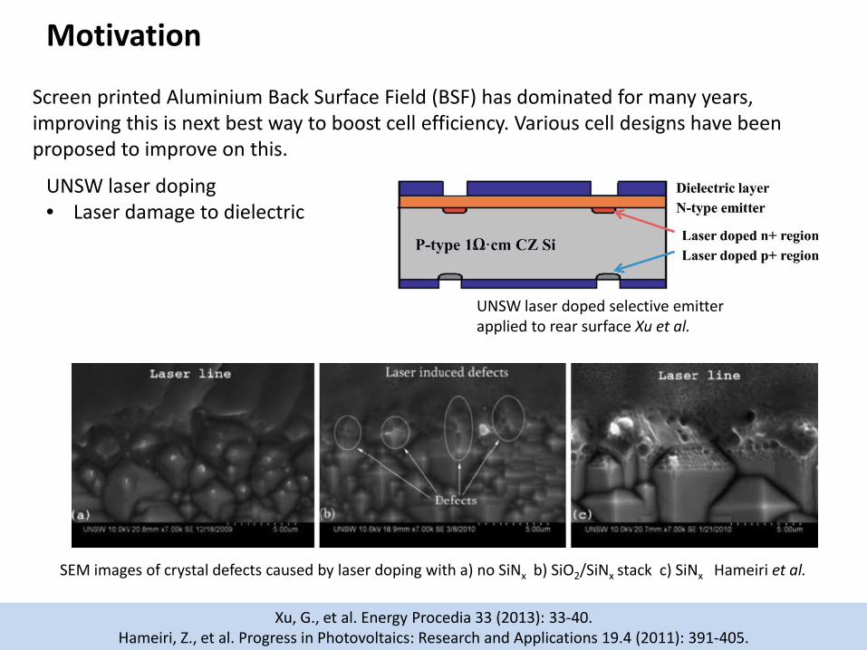
Screen printed Aluminium Back Surface Field (BSF) has dominated for many years, improving this is next best way to boost cell efficiency. Various cell designs have been proposed to improve on this.
Xu, G., et al. Energy Procedia 33 (2013): 33-40. Hameiri, Z., et al. Progress in Photovoltaics: Research and Applications 19.4 (2011): 391-405.
Motivation
UNSW laser doped selective emitter applied to rear surface Xu et al.
SEM images of crystal defects caused by laser doping with a) no SiNx b) SiO2/SiNx stack c) SiNx Hameiri et al.
UNSW laser doping • Laser damage to dielectric
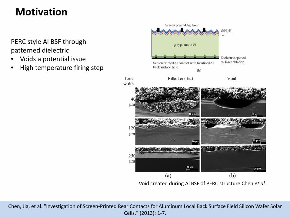
Chen, Jia, et al. "Investigation of Screen-Printed Rear Contacts for Aluminum Local Back Surface Field Silicon Wafer Solar Cells." (2013): 1-7.
Void created during Al BSF of PERC structure Chen et al.
Motivation
PERC style Al BSF through patterned dielectric • Voids a potential issue • High temperature firing step
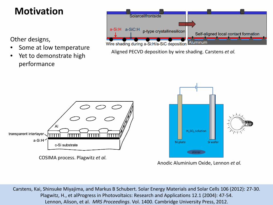
COSIMA process. Plagwitz et al.
Carstens, Kai, Shinsuke Miyajima, and Markus B Schubert. Solar Energy Materials and Solar Cells 106 (2012): 27-30. Plagwitz, H., et alProgress in Photovoltaics: Research and Applications 12.1 (2004): 47-54.
Lennon, Alison, et al. MRS Proceedings. Vol. 1400. Cambridge University Press, 2012.
Motivation
Other designs, • Some at low temperature • Yet to demonstrate high
performance
Anodic Aluminium Oxide, Lennon et al.
Aligned PECVD deposition by wire shading. Carstens et al.
Rear surface inherently difficult because: • Low doped p-type surface sensitive to surface states • Particularly for positively charged dielectric. • Creating a doped region requires high temperature Assume limited to industrial PERC or PERL type structure, we need 3 steps: • Passivate surface with dielectric • Dope Si (high temperature process, at least locally) • Metal contact through dielectric to (only) the doped region Ideally low temperature processing: cost, mc-Si, bulk hydrogenation Dielectric deposition AFTER doping process avoids thermal damage, but then need a commercially relevant way of aligning contact through the dielectric.
Motivation

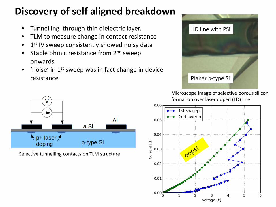
• Tunnelling through thin dielectric layer. • TLM to measure change in contact resistance • 1st IV sweep consistently showed noisy data • Stable ohmic resistance from 2nd sweep
onwards • ‘noise’ in 1st sweep was in fact change in device
resistance
LD line with PSi
Planar p-type Si
Discovery of self aligned breakdown
Selective tunnelling contacts on TLM structure
Microscope image of selective porous silicon formation over laser doped (LD) line

• Tunnelling through thin dielectric layer. • TLM to measure change in contact resistance • 1st IV sweep consistently showed noisy data • Stable ohmic resistance from 2nd sweep
onwards • ‘noise’ in 1st sweep was in fact change in device
resistance
LD line with PSi
Planar p-type Si
Discovery of self aligned breakdown
Microscope image of selective porous silicon formation over laser doped (LD) line
Selective tunnelling contacts on TLM structure

Darks spots show localised breakdown points. Lifetime reduced for increasing current – gets ‘darker’
Discovery of self aligned breakdown
Photoluminescence images of TLM structure after IV measurement
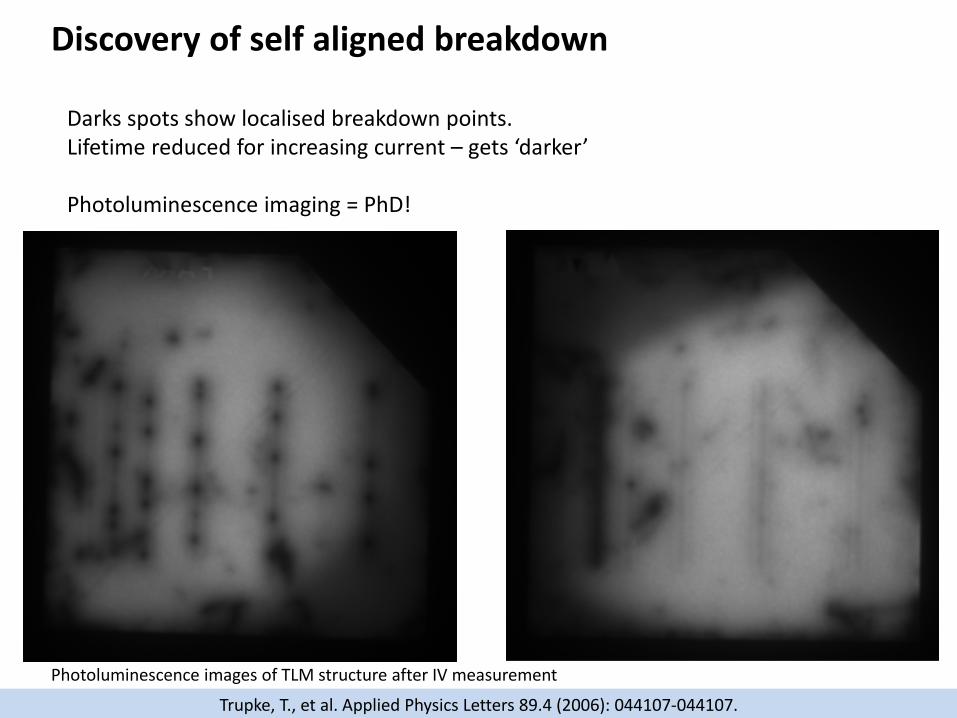
Darks spots show localised breakdown points. Lifetime reduced for increasing current – gets ‘darker’ Photoluminescence imaging = PhD!
Discovery of self aligned breakdown
Trupke, T., et al. Applied Physics Letters 89.4 (2006): 044107-044107.
Photoluminescence images of TLM structure after IV measurement
Point-contacting by Localised Dielectric Breakdown (PLDB)
• Low contact resistance < 1 mΩ.cm2 • High effective lifetime > 700mV • Processed at room temperature • Fast • Low tech • Robust

Punjab Livestock Development Board
Point-contacting by Localised Dielectric Breakdown (PLDB)
• Low contact resistance < 1 mΩ.cm2 • High effective lifetime > 700mV • Processed at room temperature • Fast • Low tech • Robust
Punjab Livestock Development Board
Point-contacting by Localised Dielectric Breakdown (PLDB)
• Low contact resistance < 1 mΩ.cm2 • High effective lifetime > 700mV • Processed at room temperature • Fast • Low tech • Robust
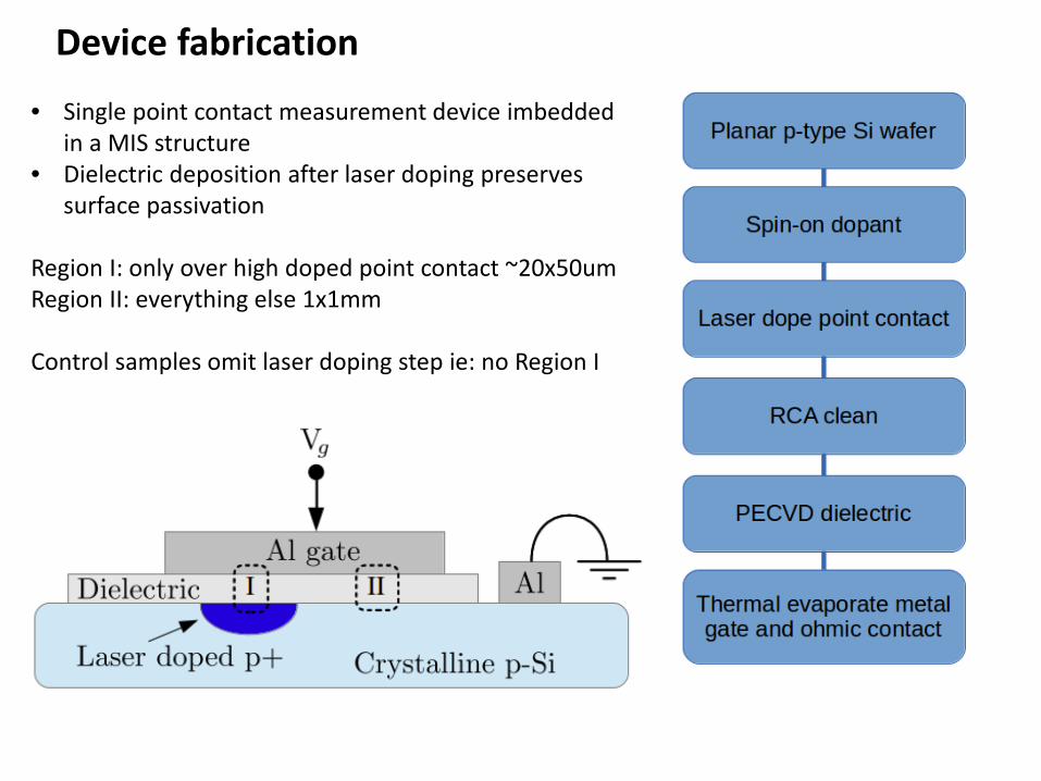
Device fabrication
• Single point contact measurement device imbedded in a MIS structure
• Dielectric deposition after laser doping preserves surface passivation
Region I: only over high doped point contact ~20x50um Region II: everything else 1x1mm Control samples omit laser doping step ie: no Region I

Outline Motivation Discovery Device fab method Basic results • DIV • TEM • MS pics Why self aligned • dielectric leakage Other applications • Other gate metals • Al BSF • Other dielectrics • n-type • With emitter Accurate measurement of Rc and Seff • p+ on n-type • Array of point-contacts Breakdown dynamics • Weibull distribution • Thickness dependence

• Sweep voltage from 0V • Abrupt breakdown in dielectric seen as
decrease in resistance • Stable linear behaviour • LD on SiNx shows similar contact
resistance compared to breakdown down technique
Typical IV results
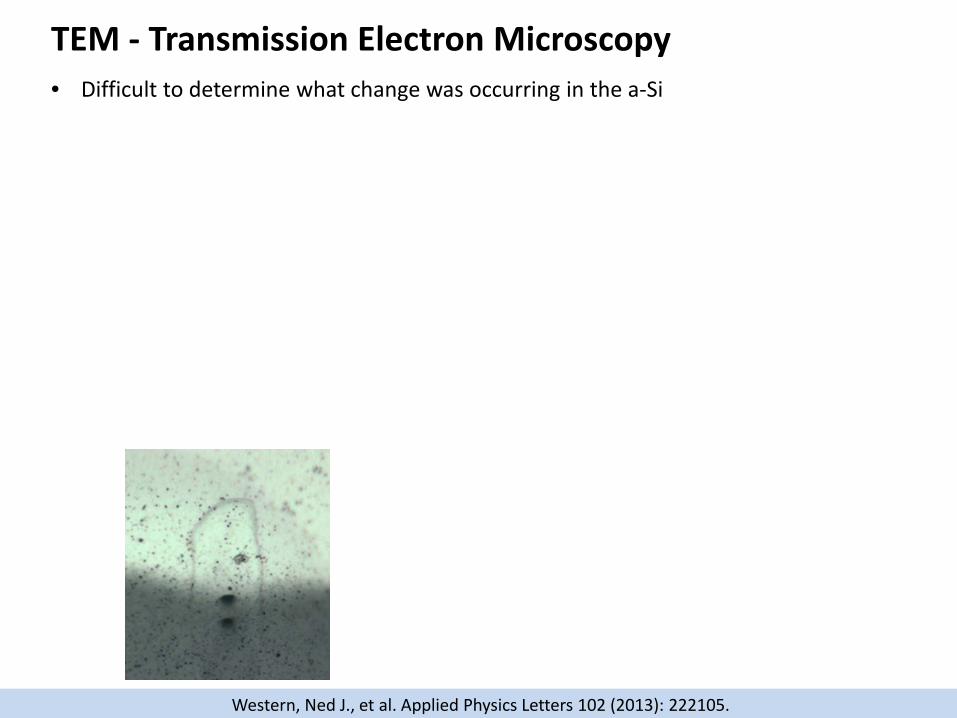
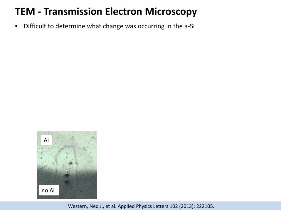
• Difficult to determine what change was occurring in the a-Si
Western, Ned J., et al. Applied Physics Letters 102 (2013): 222105.
TEM - Transmission Electron Microscopy
• Difficult to determine what change was occurring in the a-Si
Western, Ned J., et al. Applied Physics Letters 102 (2013): 222105.
TEM - Transmission Electron Microscopy
Al
no Al
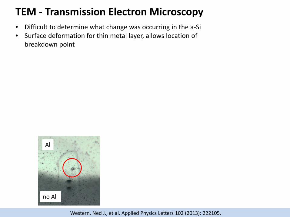
• Difficult to determine what change was occurring in the a-Si • Surface deformation for thin metal layer, allows location of
breakdown point
Western, Ned J., et al. Applied Physics Letters 102 (2013): 222105.
TEM - Transmission Electron Microscopy
Al
no Al
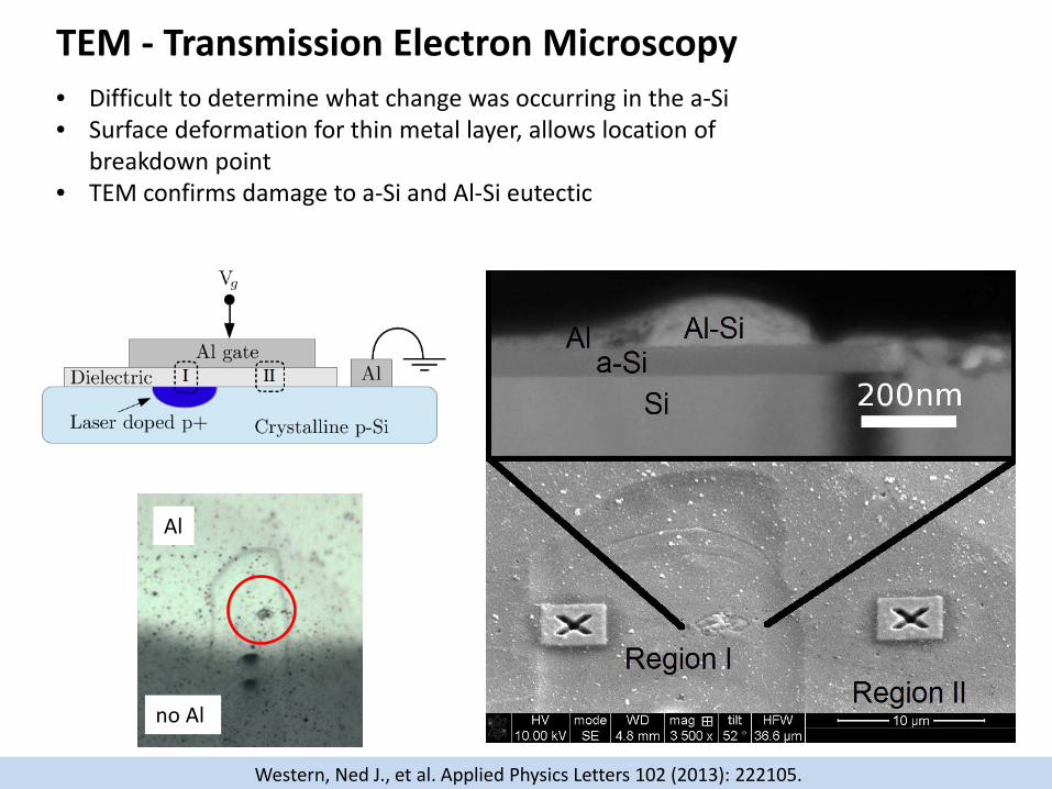
• Difficult to determine what change was occurring in the a-Si • Surface deformation for thin metal layer, allows location of
breakdown point • TEM confirms damage to a-Si and Al-Si eutectic
Western, Ned J., et al. Applied Physics Letters 102 (2013): 222105.
TEM - Transmission Electron Microscopy
Al
no Al

35mA
60mA
75mA
• Thin Al allows for convenient characterisation • Size of breakdown area increases with
increasing current • Can exceed Region I if current too high • Damage to adjacent surface passivation
Optical Microscopy

Outline Motivation Discovery Device fab method Basic results • DIV • TEM • MS pics Why self aligned • dielectric leakage Other applications • Other gate metals • Al BSF • Other dielectrics • n-type • With emitter Accurate measurement of Rc and Seff • p+ on n-type • Array of point-contacts Breakdown dynamics • Weibull distribution • Thickness dependence

• IV curve of MIS like a reversed diode
Typical IV results of control MIS devices

• IV curve of MIS like a reversed diode • Why is there current for –ve voltage?
• PF tunnelling
Typical IV results of control MIS devices
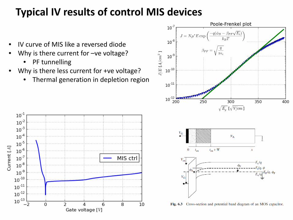
• IV curve of MIS like a reversed diode • Why is there current for –ve voltage?
• PF tunnelling • Why is there less current for +ve voltage?
• Thermal generation in depletion region
Typical IV results of control MIS devices
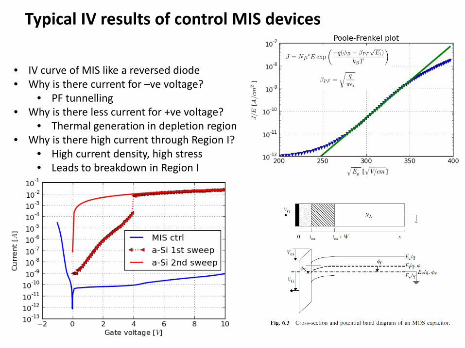
• IV curve of MIS like a reversed diode • Why is there current for –ve voltage?
• PF tunnelling • Why is there less current for +ve voltage?
• Thermal generation in depletion region • Why is there high current through Region I?
• High current density, high stress • Leads to breakdown in Region I
Typical IV results of control MIS devices

Outline Motivation Discovery Device fab method Basic results • DIV • TEM • MS pics Why self aligned • dielectric leakage Other applications • Other gate metals • Al BSF • Other dielectrics • n-type • With emitter Accurate measurement of Rc and Seff • p+ on n-type • Array of point-contacts Breakdown dynamics • Weibull distribution • Thickness dependence
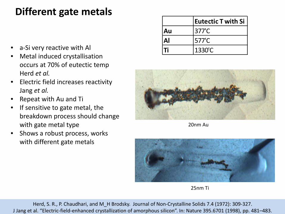
• a-Si very reactive with Al • Metal induced crystallisation
occurs at 70% of eutectic temp Herd et al.
• Electric field increases reactivity Jang et al.
• Repeat with Au and Ti • If sensitive to gate metal, the
breakdown process should change with gate metal type
• Shows a robust process, works with different gate metals
20nm Au
25nm Ti
Different gate metals
Herd, S. R., P. Chaudhari, and M_H Brodsky. Journal of Non-Crystalline Solids 7.4 (1972): 309-327. J Jang et al. “Electric-field-enhanced crystallization of amorphous silicon”. In: Nature 395.6701 (1998), pp. 481–483.
Eutectic T with SiAu 377'CAl 577'CTi 1330'C
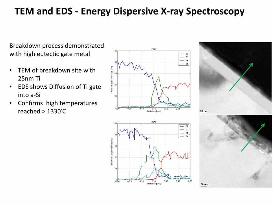
Breakdown process demonstrated with high eutectic gate metal • TEM of breakdown site with
25nm Ti • EDS shows Diffusion of Ti gate
into a-Si • Confirms high temperatures
reached > 1330’C
TEM and EDS - Energy Dispersive X-ray Spectroscopy

Not limited to boron doping Processing steps: • Injet printed Al paste lines through Si mask to
create point contact. • Belt furnace fired to create Al BSF • Wet chemistry removal of residual Al paste • Processed as for laser doped samples IV results show dielectric breakdown occurs in same way
Al doped BSF
Microscope image of injet printed Al paste on planar p-type Si
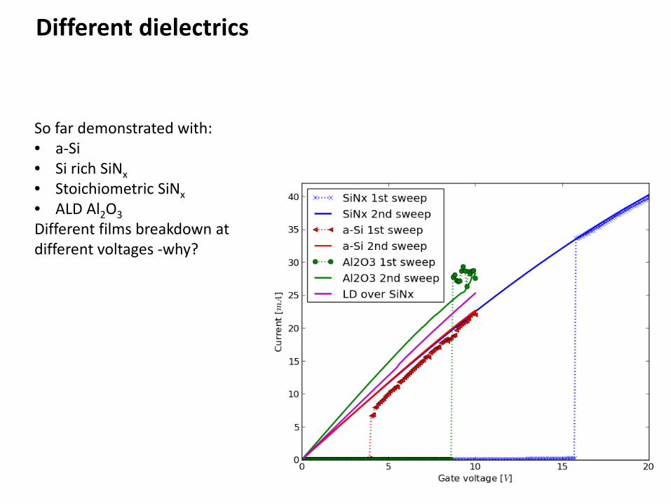
So far demonstrated with: • a-Si • Si rich SiNx • Stoichiometric SiNx • ALD Al2O3 Different films breakdown at different voltages -why?
Different dielectrics
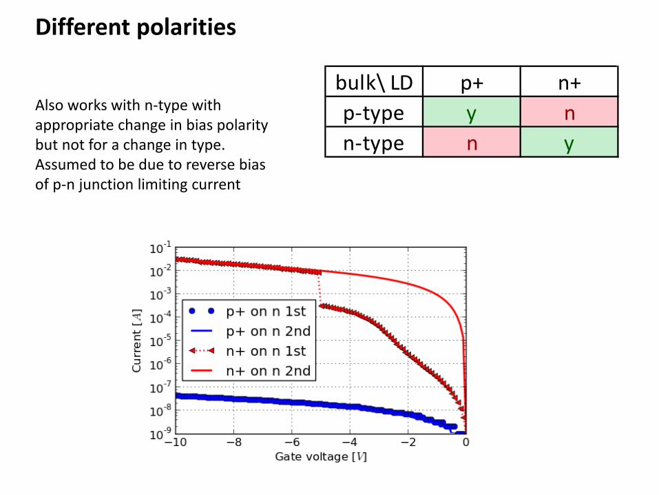
Also works with n-type with appropriate change in bias polarity but not for a change in type. Assumed to be due to reverse bias of p-n junction limiting current
bulk\ LD p+ n+p-type y nn-type n y
Different polarities
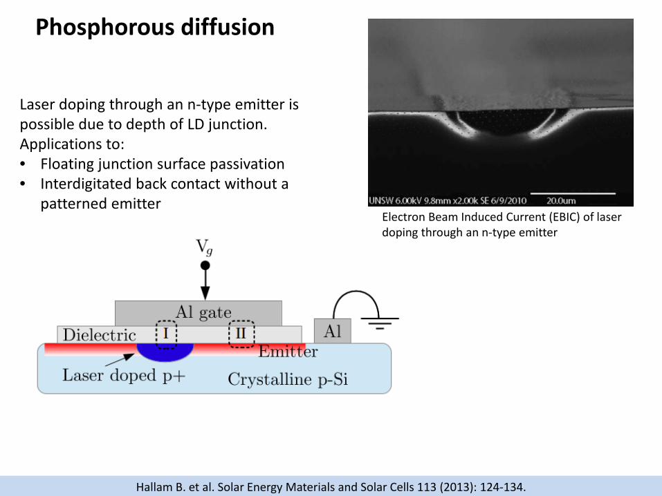
Laser doping through an n-type emitter is possible due to depth of LD junction. Applications to: • Floating junction surface passivation • Interdigitated back contact without a
patterned emitter
Hallam B. et al. Solar Energy Materials and Solar Cells 113 (2013): 124-134.
Phosphorous diffusion
Electron Beam Induced Current (EBIC) of laser doping through an n-type emitter
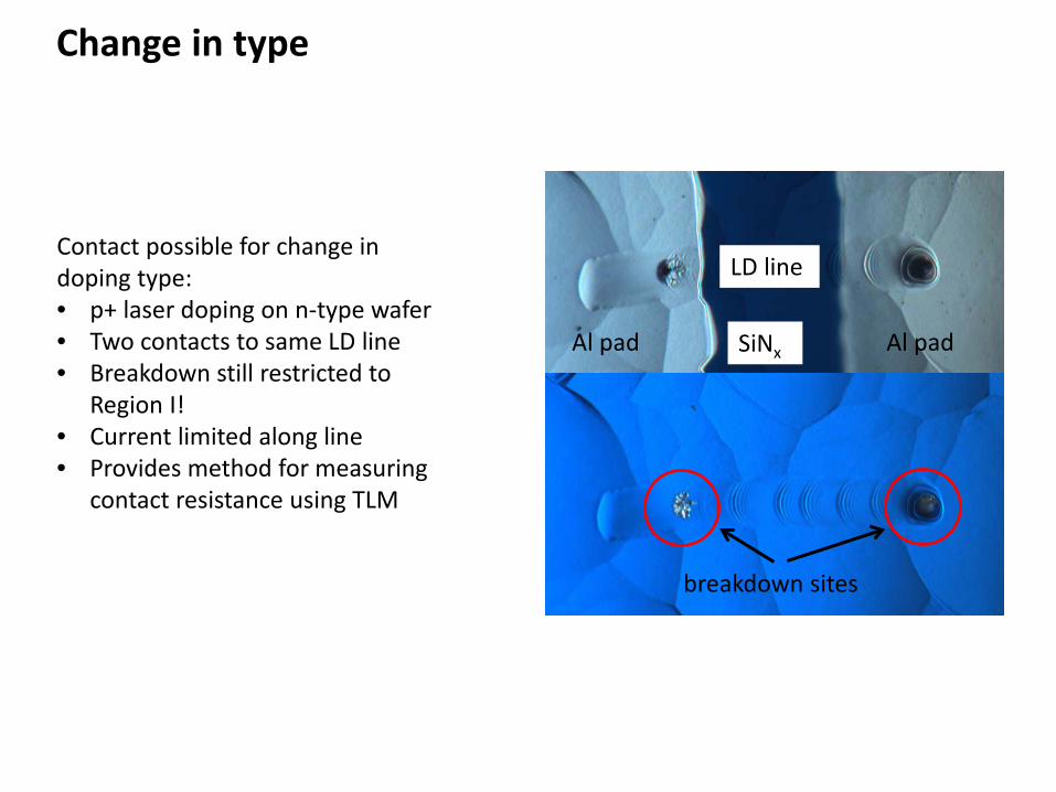
Contact possible for change in doping type: • p+ laser doping on n-type wafer • Two contacts to same LD line • Breakdown still restricted to
Region I! • Current limited along line • Provides method for measuring
contact resistance using TLM
breakdown sites
Al pad Al pad SiNx
Change in type
LD line

Outline Motivation Discovery Device fab method Basic results • DIV • TEM • MS pics Why self aligned • dielectric leakage Other applications • Other gate metals • Al BSF • Other dielectrics • n-type • With emitter Accurate measurement of Rc and Seff • p+ on n-type • Array of point-contacts Breakdown dynamics • Weibull distribution • Thickness dependence

Al
LD line
TLM – transmission line method
Multiple contacts to a single line in TLM structure. Also allows for accurate measurement of LD line conductivity!
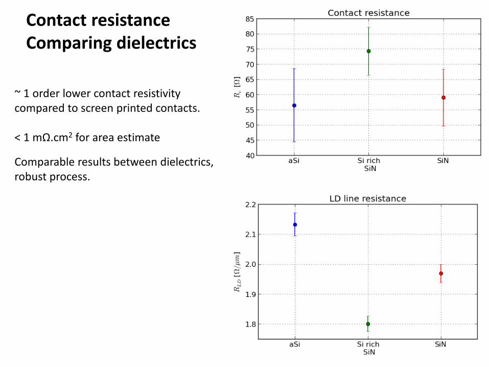
~ 1 order lower contact resistivity compared to screen printed contacts. < 1 mΩ.cm2 for area estimate Comparable results between dielectrics, robust process.
Contact resistance Comparing dielectrics
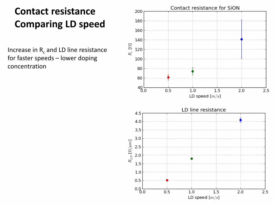
Increase in Rc and LD line resistance for faster speeds – lower doping concentration
Contact resistance Comparing LD speed

Surface passivation
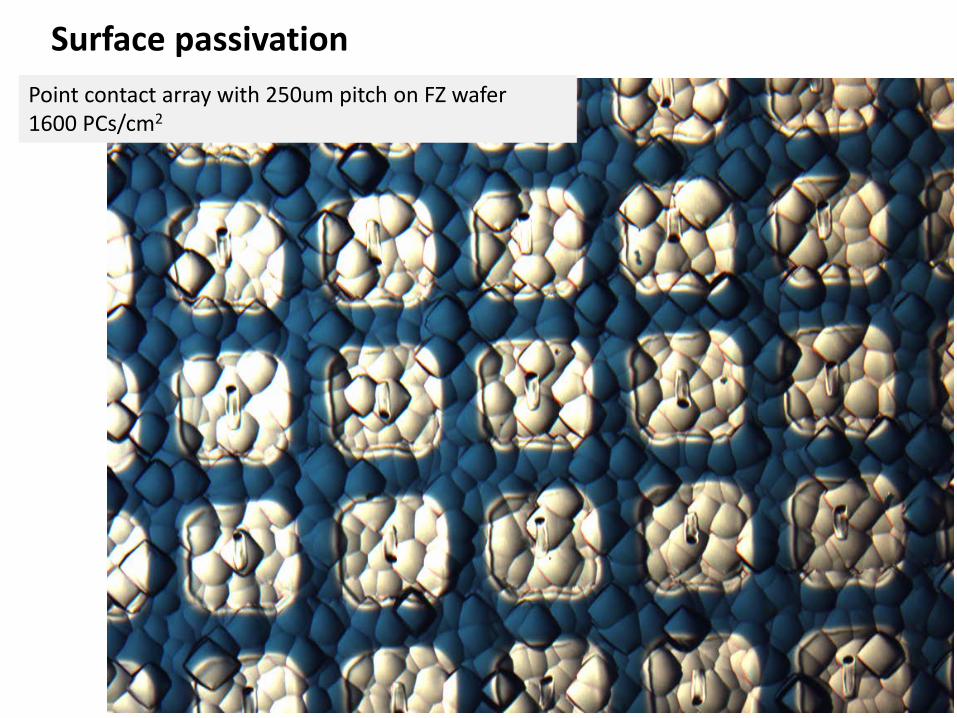
Surface passivation Point contact array with 250um pitch on FZ wafer 1600 PCs/cm2
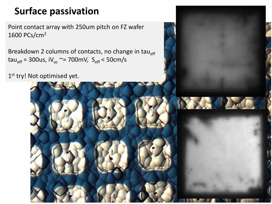
Surface passivation Point contact array with 250um pitch on FZ wafer 1600 PCs/cm2
Breakdown 2 columns of contacts, no change in taueff taueff = 300us, iVoc ~= 700mV, Seff < 50cm/s 1st try! Not optimised yet.

Outline Motivation Discovery Device fab method Basic results • DIV • TEM • MS pics Why self aligned • dielectric leakage Other applications • Other gate metals • Al BSF • Other dielectrics • n-type • With emitter Accurate measurement of Rc and Seff • p+ on n-type • Array of point-contacts Breakdown dynamics • Weibull distribution • Thickness dependence
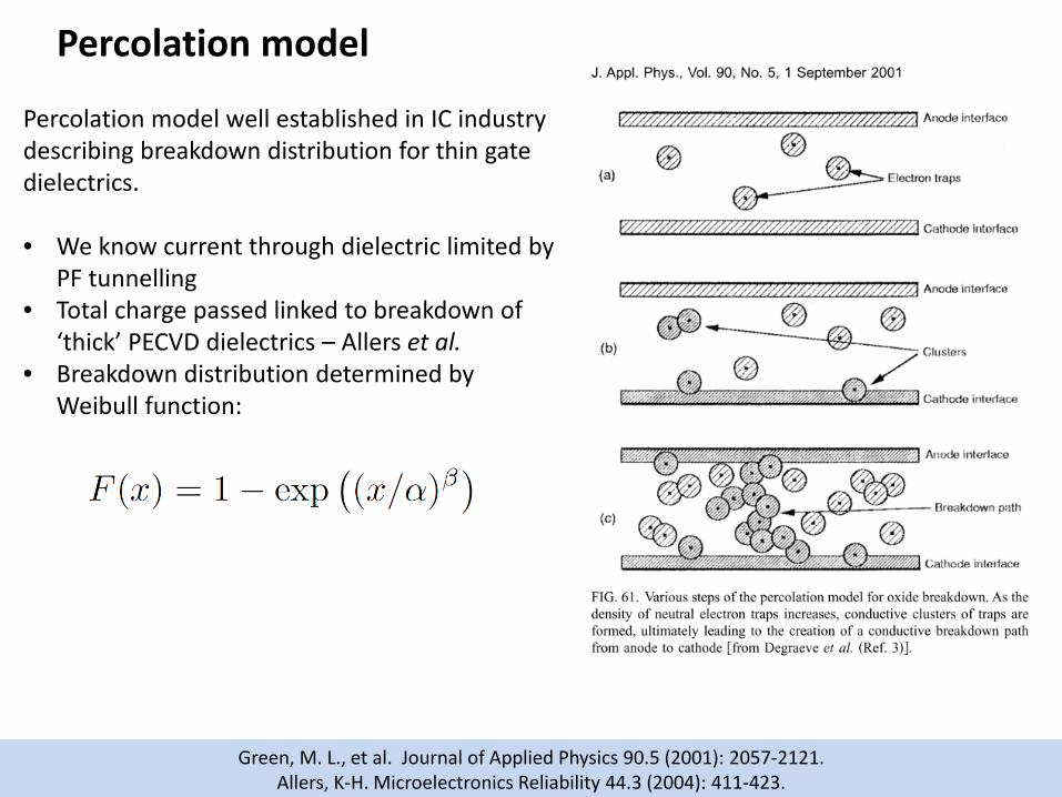
Percolation model well established in IC industry describing breakdown distribution for thin gate dielectrics. • We know current through dielectric limited by
PF tunnelling • Total charge passed linked to breakdown of
‘thick’ PECVD dielectrics – Allers et al. • Breakdown distribution determined by
Weibull function:
Percolation model
Green, M. L., et al. Journal of Applied Physics 90.5 (2001): 2057-2121. Allers, K-H. Microelectronics Reliability 44.3 (2004): 411-423.

Breakdown voltage extracted from each IV sweep, then added to ‘Weibull plot’. Fit to function, can extract Weibull parameter β
Weibull distribution
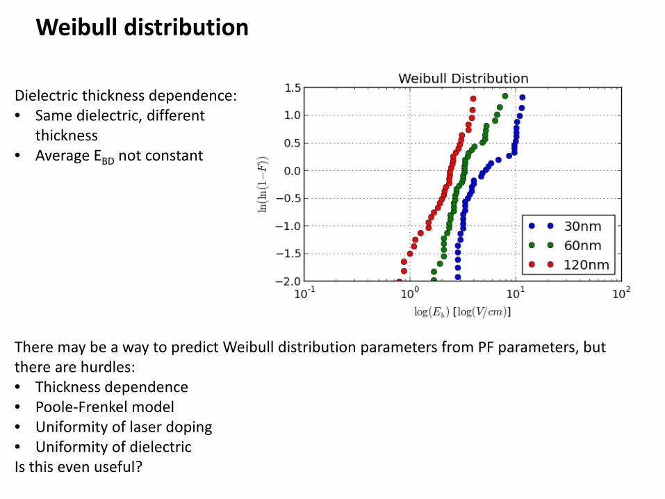
There may be a way to predict Weibull distribution parameters from PF parameters, but there are hurdles: • Thickness dependence • Poole-Frenkel model • Uniformity of laser doping • Uniformity of dielectric Is this even useful?
Dielectric thickness dependence: • Same dielectric, different
thickness • Average EBD not constant
Weibull distribution

• Link leakage current to breakdown characteristics (maybe) • Optimise for Seff and Rc • Apply to a rear surface of high efficiency solar cell • Transfer to industry • Apply to IBC cell • Apply to high performance mc-Si • Get working for front surface selective emitter structure
Future Work

Acknowledgements
• The authors acknowledge the facilities, and the scientific and technical assistance of the Australian Microscopy & Microanalysis Research Facility at the Electron Microscope Unit, The University of New South Wales.
• This work was performed in part at the NSW Node of the Australian National Fabrication Facility
• This Program has been supported by the Australian Government through the Australian Renewable Energy Agency (ARENA). Responsibility for the views, information or advice expressed herein is not accepted by the Australian Government.

Questions?
Related Documents