12-Bit, 10µS H ybrid AD C
H S AD C85D ata Converter Line
FEATURES
• –55ºC to +125ºC Operation• M IL-STD-883 Processing• 10 µS Conversion Time• Low Power, 1.32W (max)• Replacement for A DC85/84 and A DC-HX12B/HZ12B
DESCRIPTION
The HS A DC85 is specif ically designed to replacethe A DC581,. A DC85/84 and A DC-HX12B/HZ12B.Complete with internal clock, reference and inputbuffer amplif ier, the HS A DC85 can also be usedwith an external clock for synchronization (seeEXTERNA L CLOCK section under A PPLICA TIONSINFORM A TION). Conversion speeds of 10 µs for 12-Bit operation and 8 µs for 10-Bit operation allowsthe HS A DC85 to be used in a wide range ofapplications. Short cycle and internal clock ratemay also be externally adjusted to provide fasterconversion speeds at lower resolutions. Gain andoffset can be externally trimmed to zero,providing full-scale accuracy of ±0.012% ±1/2 LSB.Data is obtainable in both parallel and serial formwith corresponding clock and status signals.Digital input and output signals are DTL/TTLcompatible. Other features include:
Low Power — A 33% reduction in powerdissipation allows the HS A DC85 to operatereliably at high temperatures without failure dueto excessive package heating. Total powerconsumed is only 1.32 W maximum.
Selectable Input Ranges — Input scaling resistorsallow the selection of input ranges of ±2.5V , ±5V ,±10V , 0 to +5V or 0 to +10V .
Reliability — Packaged in a 32-pin hermetically sealedcase and utilizing advanced devices and laser-trimmed thin f ilm resistors, the HS A DC85 is one ofthe most reliable analog-to-digital converters to date.Specif ied over the –55ºC to +125ºC temperaturerange, it has a low linearity drif t specif ication of only±2 ppm/ºC maximum. A ll “ B” versions of the HSA DC85 series are fully screened and tested to M IL-STD-883 Rev. C, Level B requirements.
20
32
14
21
17
19
18
29
30
STA TUS
SERIA L OUT
SHORT CY CLE
STA RT
CLOCKRA TE CONTROLCLOCK OUT
REF OUT
BUFFER OUT
BUFFER IN
FUNCTIONAL DIAGRAM
131 2 3 4 5 6 7 8 9 10 11 12LSB M SB M SB
SA R
DA C
COM P
CLOCK
REF–
+
–
+
26
31
15
16
28
A NA GND
DIG GND
+5V
– 5V
– 15V
27 24 25 23 22
GA IN 10V 20V BIPOLA R
165Cedar Hill Street,Marlborough,MA01752 Tel:508.485.6350 Fax: 508.485.5168www.SpectrumMicrowave.com

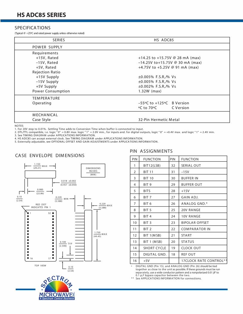
SPECIFICATIO N S(Typical @ +25ºC and rated power supply unless otherwise noted)
SERIES HSA DC85
TY PE Successive A pproximation
RESOLUTION 12-Bits
A NA LOG INPUTSBipolar Ranges ±2.5V . ±5V . ±10VUnipolar Ranges 0 to +5V , 0 to +10VImpedance (Direct Input) 300 / V oltBuffer A mplif ier
Impedance 100M (min)Bias Current 50 nASettling Time1 2 µS
DIGITA L INPUTS2
Start Positive Pulse 50nS W ide (min). Trailing Edge(“ 1” to “ 0” ) Initiates Conversion3
Logic Loading 1 TTL LoadExternal Clock Optional4
DIGITA L OUTPUTS2
Parallel DataOutput Codes
Unipolar Comp. Straight Bin.Bipolar Comp. Offset Bin., Comp, Two's Comp.
Output Drive 2 TTL Loads (min)Serial (Non Return to Zero) Data
Output Codes Comp. Straight Bin., Comp. Offset Bin.Output Drive 2 TTL Loads (min)
Status Logic “ 1” During ConversionStatus Output Drive 2 TTL Loads (min)
Clock Out4
Output Drive 2 TTL Loads (min)Frequency 1.4 M Hz
REFERENCE Internal +6.2V ±5%Ref Out 200 µA M aximum with no Degradation of SpecsDrif t ±10ppm/ºC (max)
CONV ERSION TIM E/THROUGHPUT RA TE 8.8 µS, Typ; 10 µS, max/100 kHz
A CCURA CY @ 25ºCQuantization ±1/2LSBLinearity ±0.012% of F.S.R. (max)Offset5
Unipolar ±0.05% of F.S.R.Bipolar ±0.1% of F.S.R.(max)
Gain5 ±0.1% of F.S.R.M onotonicity No M issing Codes
STA BILITYLinearity
–25ºC to +85ºC ±1 ppm/ºC; ±2 ppm/ºC, (max)–55ºC to +125ºC ±2 ppm/ºC. (max)
Scale Factor (Gain)–25ºC to +85ºC ±8 ppm/ºC; ±15 ppm/ºC, (max)–55ºC to +125ºC ±20 ppm/ºC, (max)
Offset (Unipolar)–25ºC to +85ºC ±2 ppm/ºC; ±3 ppm/ºC, (max)–55ºC to +125ºC ±3 ppm/ºC. (max)
Offset (Bipolar)–25ºC to +85ºC ±4 ppm/ºC; ±7 ppm/ºC. (max)–55ºC to +125ºC ±12 ppm/ºC, (max)
Total Transfer A ccuracy–25ºC to +85ºC ±10 ppm/ºC; ±20 ppm/ºC. (max)–55ºC to +125ºC ±30 ppm/ºC, (max)
HS ADC85 SERIES
Continued on next page.
SPECIFICA TIONS(Typical @ +25ºC and rated power supply unless otherwise noted)
SERIES HS A DC85
POW ER SUPPLY
Requirements+15V , Rated +14.25 to +15.75V @ 28 mA (max)–15V , Rated –14.25V to+15.75V @ 30 mA (max)+5V , Rated +4.75V to +5.25V @ 91 mA (max)
Rejection Ratio+15V Supply ±0.005% F.S.R,/% V s–15V Supply ±0.005% F.S.R,/% V s+5V Supply ±0.002% F.S.R,/% V s
Power Consumption 1.32W (max)
TEM PERA TUREOperating –55ºC to +125ºC B V ersion
ºC to 70ºC C V ersion
M ECHA NICA LCase Style 32-Pin Hermetic M etal
NOTES1. For 20V step to 0.01% . Settling Time adds to Conversion Time when buffer is connected to input.2. DTL/TTL compatible, i.e. logic “ 0” = 0.8V max. logic “ 1” = 2.0V min., for inputs and. for digital outputs, logic “ 0” = +0.4V max. and logic “ 1” = 2.4V min.3. See TIM ING DIA GRA M under A PPLICA TIONS INFORM A TION.4. HS A DC85 can accept external clock. See TIM ING DIA GRA M under A PPLICA TIONS INFORM A TION.5. Externally adjustable, see OPTIONA L OFFSET A ND GA IN A DJUSTM ENTS under A PPLICA TIONS INFORM A TION.
CA SE ENV ELOPE DIM ENSIONS
1.150
(29.21)M A X
0.900
(22.86)
0.220
(5.588)M IN
0.018 ±0.002
(0.457 ±0.050)
0.220
(5.588)M A X
1.750
(44.45)M A X
0.100
(2.540)TY P
0.10
(2.54)
TOP V IEW
RED DOTINDICA TES PIN 1
DIM ENSIONSINCHES
(M M )
0.10
(2.54)
1 32
16 17
PIN FUNCTION PIN FUNCTION
1 BIT12(LSB) 32 SERIA L OUT
2 BIT 11 31 –15V
3 BIT 10 30 BUFFER IN
4 BIT 9 29 BUFFER OUT
5 BITS 28 +15V
6 BIT 7 27 GA IN A DJ.
7 BIT 6 26 A NA LOG GND.*
8 BIT 5 25 20V RA NGE
9 BIT 4 24 10V RA NGE
10 BIT 3 23 BIPOLA R OFFSET
11 BIT 2 22 COM PA RA TOR IN
12 BIT 1(M SB) 21 STA RT
13 BIT 1 (M SB) 20 STA TUS
14 SHORT CY CLE 19 CLOCK OUT
15 DIGITA L GND. 18 REF OUT
16 +5V 17CLOCK RA TE CONTROL* *
• DIGITA L GND (Pin 15), and A NA LOG GND (Pin 26) should be tiedtogether as close to the unit as possible. If these grounds must be runseparately, use a wide conductor pattern and a nonpolarized 0.01 jiF to0.1 p,F bypass capacitor between the two.
* * See A PPLICA TIONS INFORM A TION for connections.
PIN A SSIGNM ENTS
HS ADC85 SERIES


![ADC-20 und ADC-24 › download › datasheets › adc20...Datenlogger ADC-20 und ADC-24 ADC-20 ADC-24 Auflösung 20 Bit 24 Bit Anzahl Kanäle[1] 4 differenzial / 8 einpolig 8 differenzial](https://static.cupdf.com/doc/110x72/5f23cbdc98bf2e58da663aad/adc-20-und-adc-24-a-download-a-datasheets-a-adc20-datenlogger-adc-20-und.jpg)