12-Bit, 10μS Hybrid ADC HS ADC85 Data Converter Line FEATURES • –55ºC to +125ºC Operation • MIL-STD-883 Processing • 10 μS Conversion Time • Low Power, 1.32W (max) • Replacement for ADC85/84 and ADC-HX12B/HZ12B DESCRIPTION The HS ADC85 is specifically designed to replace the ADC581,. ADC85/84 and ADC-HX12B/HZ12B. Complete with internal clock, reference and input buffer amplifier, the HS ADC85 can also be used with an external clock for synchronization (see EXTERNAL CLOCK section under APPLICATIONS INFORMATION). Conversion speeds of 10 μs for 12- Bit operation and 8 μs for 10-Bit operation allows the HS ADC85 to be used in a wide range of applications. Short cycle and internal clock rate may also be externally adjusted to provide faster conversion speeds at lower resolutions. Gain and offset can be externally trimmed to zero, providing full-scale accuracy of ±0.012% ±1/2 LSB. Data is obtainable in both parallel and serial form with corresponding clock and status signals. Digital input and output signals are DTL/TTL compatible. Other features include: Low Power — A 33% reduction in power dissipation allows the HS ADC85 to operate reliably at high temperatures without failure due to excessive package heating. Total power consumed is only 1.32 W maximum. Selectable Input Ranges — Input scaling resistors allow the selection of input ranges of ±2.5V, ±5V, ±10V, 0 to +5V or 0 to +10V. Reliability—Packaged in a 32-pin hermetically sealed case and utilizing advanced devices and laser- trimmed thin film resistors, the HS ADC85 is one of the most reliable analog-to-digital converters to date. Specified over the –55ºC to +125ºC temperature range, it has a low linearity drift specification of only ±2 ppm/ºC maximum. All “ B” versions of the HS ADC85 series are fully screened and tested to MIL- STD-883 Rev. C, Level B requirements. 20 32 14 21 17 19 18 29 30 STATUS SERIAL OUT SHORT CYCLE START CLOCK RATE CONTROL CLOCK OUT REF OUT BUFFER OUT BUFFER IN FUNCTIONAL DIAGRAM 13 1 2 3 4 5 6 7 8 9 10 11 12 LSB MSBMSB SAR DAC COMP CLOCK REF – + – + 26 31 15 16 28 ANA GND DIG GND +5V – 5V – 15V 27 24 25 23 22 GAIN 10V 20V BIPOLAR 165 Cedar Hill Street, Marlborough, MA 01752 Tel: 508.485.6350 Fax: 508.485.5168 www.SpectrumMicrowave.com

Welcome message from author
This document is posted to help you gain knowledge. Please leave a comment to let me know what you think about it! Share it to your friends and learn new things together.
Transcript

12-Bit, 10µS H ybrid AD C
H S AD C85D ata Converter Line
FEATURES
• –55ºC to +125ºC Operation• M IL-STD-883 Processing• 10 µS Conversion Time• Low Power, 1.32W (max)• Replacement for A DC85/84 and A DC-HX12B/HZ12B
DESCRIPTION
The HS A DC85 is specif ically designed to replacethe A DC581,. A DC85/84 and A DC-HX12B/HZ12B.Complete with internal clock, reference and inputbuffer amplif ier, the HS A DC85 can also be usedwith an external clock for synchronization (seeEXTERNA L CLOCK section under A PPLICA TIONSINFORM A TION). Conversion speeds of 10 µs for 12-Bit operation and 8 µs for 10-Bit operation allowsthe HS A DC85 to be used in a wide range ofapplications. Short cycle and internal clock ratemay also be externally adjusted to provide fasterconversion speeds at lower resolutions. Gain andoffset can be externally trimmed to zero,providing full-scale accuracy of ±0.012% ±1/2 LSB.Data is obtainable in both parallel and serial formwith corresponding clock and status signals.Digital input and output signals are DTL/TTLcompatible. Other features include:
Low Power — A 33% reduction in powerdissipation allows the HS A DC85 to operatereliably at high temperatures without failure dueto excessive package heating. Total powerconsumed is only 1.32 W maximum.
Selectable Input Ranges — Input scaling resistorsallow the selection of input ranges of ±2.5V , ±5V ,±10V , 0 to +5V or 0 to +10V .
Reliability — Packaged in a 32-pin hermetically sealedcase and utilizing advanced devices and laser-trimmed thin f ilm resistors, the HS A DC85 is one ofthe most reliable analog-to-digital converters to date.Specif ied over the –55ºC to +125ºC temperaturerange, it has a low linearity drif t specif ication of only±2 ppm/ºC maximum. A ll “ B” versions of the HSA DC85 series are fully screened and tested to M IL-STD-883 Rev. C, Level B requirements.
20
32
14
21
17
19
18
29
30
STA TUS
SERIA L OUT
SHORT CY CLE
STA RT
CLOCKRA TE CONTROLCLOCK OUT
REF OUT
BUFFER OUT
BUFFER IN
FUNCTIONAL DIAGRAM
131 2 3 4 5 6 7 8 9 10 11 12LSB M SB M SB
SA R
DA C
COM P
CLOCK
REF–
+
–
+
26
31
15
16
28
A NA GND
DIG GND
+5V
– 5V
– 15V
27 24 25 23 22
GA IN 10V 20V BIPOLA R
165Cedar Hill Street,Marlborough,MA01752 Tel:508.485.6350 Fax: 508.485.5168www.SpectrumMicrowave.com

SPECIFICATIO N S(Typical @ +25ºC and rated power supply unless otherwise noted)
SERIES HSA DC85
TY PE Successive A pproximation
RESOLUTION 12-Bits
A NA LOG INPUTSBipolar Ranges ±2.5V . ±5V . ±10VUnipolar Ranges 0 to +5V , 0 to +10VImpedance (Direct Input) 300 / V oltBuffer A mplif ier
Impedance 100M (min)Bias Current 50 nASettling Time1 2 µS
DIGITA L INPUTS2
Start Positive Pulse 50nS W ide (min). Trailing Edge(“ 1” to “ 0” ) Initiates Conversion3
Logic Loading 1 TTL LoadExternal Clock Optional4
DIGITA L OUTPUTS2
Parallel DataOutput Codes
Unipolar Comp. Straight Bin.Bipolar Comp. Offset Bin., Comp, Two's Comp.
Output Drive 2 TTL Loads (min)Serial (Non Return to Zero) Data
Output Codes Comp. Straight Bin., Comp. Offset Bin.Output Drive 2 TTL Loads (min)
Status Logic “ 1” During ConversionStatus Output Drive 2 TTL Loads (min)
Clock Out4
Output Drive 2 TTL Loads (min)Frequency 1.4 M Hz
REFERENCE Internal +6.2V ±5%Ref Out 200 µA M aximum with no Degradation of SpecsDrif t ±10ppm/ºC (max)
CONV ERSION TIM E/THROUGHPUT RA TE 8.8 µS, Typ; 10 µS, max/100 kHz
A CCURA CY @ 25ºCQuantization ±1/2LSBLinearity ±0.012% of F.S.R. (max)Offset5
Unipolar ±0.05% of F.S.R.Bipolar ±0.1% of F.S.R.(max)
Gain5 ±0.1% of F.S.R.M onotonicity No M issing Codes
STA BILITYLinearity
–25ºC to +85ºC ±1 ppm/ºC; ±2 ppm/ºC, (max)–55ºC to +125ºC ±2 ppm/ºC. (max)
Scale Factor (Gain)–25ºC to +85ºC ±8 ppm/ºC; ±15 ppm/ºC, (max)–55ºC to +125ºC ±20 ppm/ºC, (max)
Offset (Unipolar)–25ºC to +85ºC ±2 ppm/ºC; ±3 ppm/ºC, (max)–55ºC to +125ºC ±3 ppm/ºC. (max)
Offset (Bipolar)–25ºC to +85ºC ±4 ppm/ºC; ±7 ppm/ºC. (max)–55ºC to +125ºC ±12 ppm/ºC, (max)
Total Transfer A ccuracy–25ºC to +85ºC ±10 ppm/ºC; ±20 ppm/ºC. (max)–55ºC to +125ºC ±30 ppm/ºC, (max)
HS ADC85 SERIES
Continued on next page.
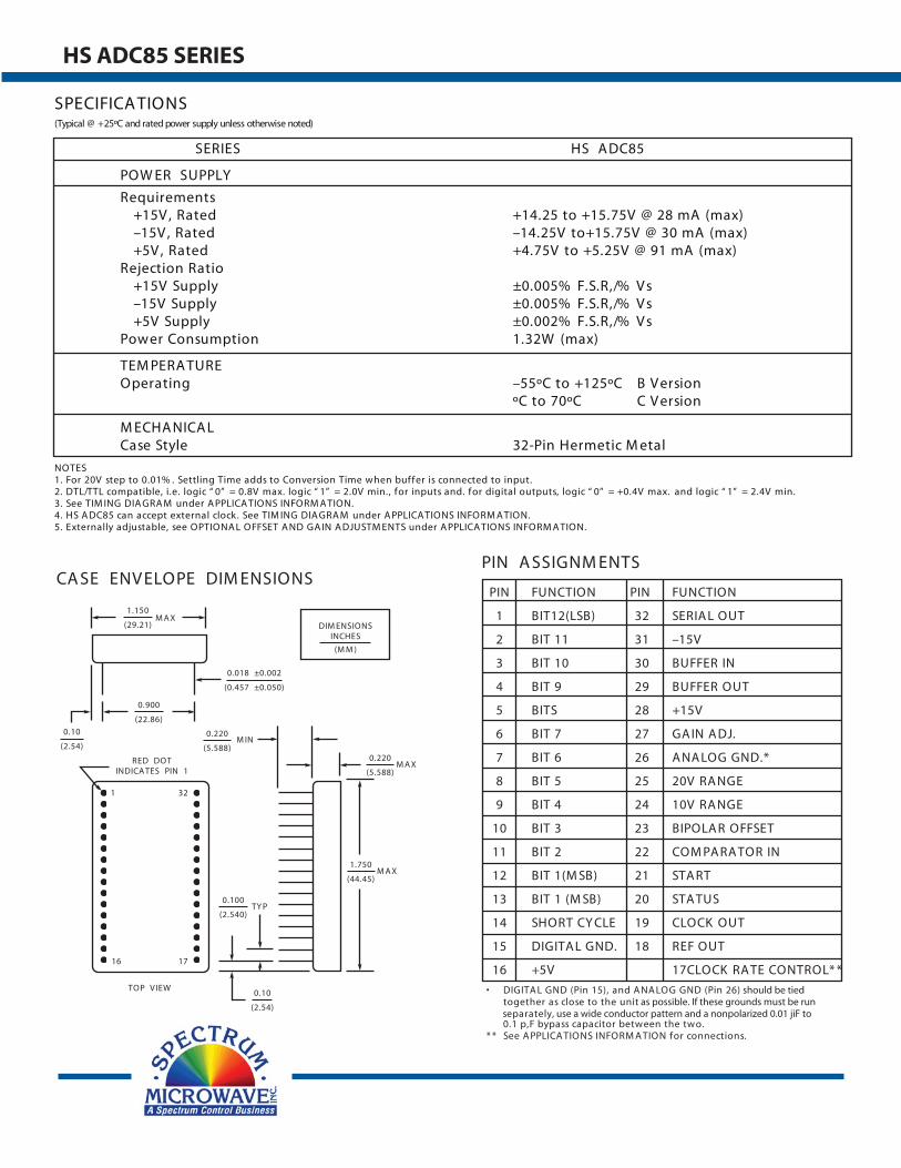
SPECIFICA TIONS(Typical @ +25ºC and rated power supply unless otherwise noted)
SERIES HS A DC85
POW ER SUPPLY
Requirements+15V , Rated +14.25 to +15.75V @ 28 mA (max)–15V , Rated –14.25V to+15.75V @ 30 mA (max)+5V , Rated +4.75V to +5.25V @ 91 mA (max)
Rejection Ratio+15V Supply ±0.005% F.S.R,/% V s–15V Supply ±0.005% F.S.R,/% V s+5V Supply ±0.002% F.S.R,/% V s
Power Consumption 1.32W (max)
TEM PERA TUREOperating –55ºC to +125ºC B V ersion
ºC to 70ºC C V ersion
M ECHA NICA LCase Style 32-Pin Hermetic M etal
NOTES1. For 20V step to 0.01% . Settling Time adds to Conversion Time when buffer is connected to input.2. DTL/TTL compatible, i.e. logic “ 0” = 0.8V max. logic “ 1” = 2.0V min., for inputs and. for digital outputs, logic “ 0” = +0.4V max. and logic “ 1” = 2.4V min.3. See TIM ING DIA GRA M under A PPLICA TIONS INFORM A TION.4. HS A DC85 can accept external clock. See TIM ING DIA GRA M under A PPLICA TIONS INFORM A TION.5. Externally adjustable, see OPTIONA L OFFSET A ND GA IN A DJUSTM ENTS under A PPLICA TIONS INFORM A TION.
CA SE ENV ELOPE DIM ENSIONS
1.150
(29.21)M A X
0.900
(22.86)
0.220
(5.588)M IN
0.018 ±0.002
(0.457 ±0.050)
0.220
(5.588)M A X
1.750
(44.45)M A X
0.100
(2.540)TY P
0.10
(2.54)
TOP V IEW
RED DOTINDICA TES PIN 1
DIM ENSIONSINCHES
(M M )
0.10
(2.54)
1 32
16 17
PIN FUNCTION PIN FUNCTION
1 BIT12(LSB) 32 SERIA L OUT
2 BIT 11 31 –15V
3 BIT 10 30 BUFFER IN
4 BIT 9 29 BUFFER OUT
5 BITS 28 +15V
6 BIT 7 27 GA IN A DJ.
7 BIT 6 26 A NA LOG GND.*
8 BIT 5 25 20V RA NGE
9 BIT 4 24 10V RA NGE
10 BIT 3 23 BIPOLA R OFFSET
11 BIT 2 22 COM PA RA TOR IN
12 BIT 1(M SB) 21 STA RT
13 BIT 1 (M SB) 20 STA TUS
14 SHORT CY CLE 19 CLOCK OUT
15 DIGITA L GND. 18 REF OUT
16 +5V 17CLOCK RA TE CONTROL* *
• DIGITA L GND (Pin 15), and A NA LOG GND (Pin 26) should be tiedtogether as close to the unit as possible. If these grounds must be runseparately, use a wide conductor pattern and a nonpolarized 0.01 jiF to0.1 p,F bypass capacitor between the two.
* * See A PPLICA TIONS INFORM A TION for connections.
PIN A SSIGNM ENTS
HS ADC85 SERIES
Related Documents


![ADC-20 und ADC-24 › download › datasheets › adc20...Datenlogger ADC-20 und ADC-24 ADC-20 ADC-24 Auflösung 20 Bit 24 Bit Anzahl Kanäle[1] 4 differenzial / 8 einpolig 8 differenzial](https://static.cupdf.com/doc/110x72/5f23cbdc98bf2e58da663aad/adc-20-und-adc-24-a-download-a-datasheets-a-adc20-datenlogger-adc-20-und.jpg)


