1 CS/ECE 5710/6710 Introduction to Layout Inverter Layout Example Layout Design Rules Composite Layout Drawing the mask layers that will be used by the fabrication folks to make the devices Very different from schematics In schematics you’re describing the LOGICAL connections In layout, you’re describing the PHYSICAL placement of everything! Use colored regions to define the different layers that are patterned onto the silicon N-type Transistor + - i electrons Vds +Vgs S G D N-type from the top Top view shows patterns that make up the transistor Diffusion Mask Mask for just the diffused regions Polysilicon Mask Mask for just the polysilicon areas

Welcome message from author
This document is posted to help you gain knowledge. Please leave a comment to let me know what you think about it! Share it to your friends and learn new things together.
Transcript

1
CS/ECE 5710/6710
Introduction to Layout Inverter Layout Example
Layout Design Rules
Composite Layout Drawing the mask layers that will be used
by the fabrication folks to make the devices Very different from schematics
In schematics you’re describing the LOGICAL connections
In layout, you’re describing the PHYSICAL placement of everything!
Use colored regions to define the different layers that are patterned onto the silicon
N-type Transistor
+
-
i electrons Vds
+Vgs S
G
D
N-type from the top
Top view shows patterns that make up the transistor
Diffusion Mask
Mask for just the diffused regions
Polysilicon Mask
Mask for just the polysilicon areas

2
Diffusion (active) Mask
Diffused (active) mask is actually drawn as a solid rectangle
Polysilicon Mask
Polysilicon mask goes on top of the active
Combine the two masks
You get an N-type transistor There are other steps in the process…
P-type transistor
Same type of masks as the N-type But, you have to get the substrate right and you have to dope the diffusion differently
General CMOS cross section
Note that the general substrate is P-type The N-substrate for the P-transistor is in a “well” There are lots of other layers
Thick SiO2 oxide (“field oxide) Thin SiO2 oxide (gate oxide Metal for interconnect
Cutaway Photo
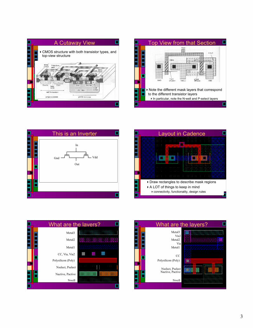
3
A Cutaway View CMOS structure with both transistor types, and
top-view structure
Top View from that Section
Note the different mask layers that correspond to the different transistor layers In particular, note the N-well and P-select layers
This is an Inverter
In
Out
Gnd Vdd
Layout in Cadence
Each color corresponds to a mask layer Draw rectangles to describe mask regions A LOT of things to keep in mind
connectivity, functionality, design rules
What are the layers?
Nwell
Nactive, Pactive
Nselect, Pselect
Polysilicon (Poly)
CC, Via, Via2
Metal1
Metal2
Metal3
What are the layers?
Nwell
Nactive, Pactive Nselect, Pselect
Polysilicon (Poly) CC
Metal1
Metal2
Metal3
Via
Via2
4
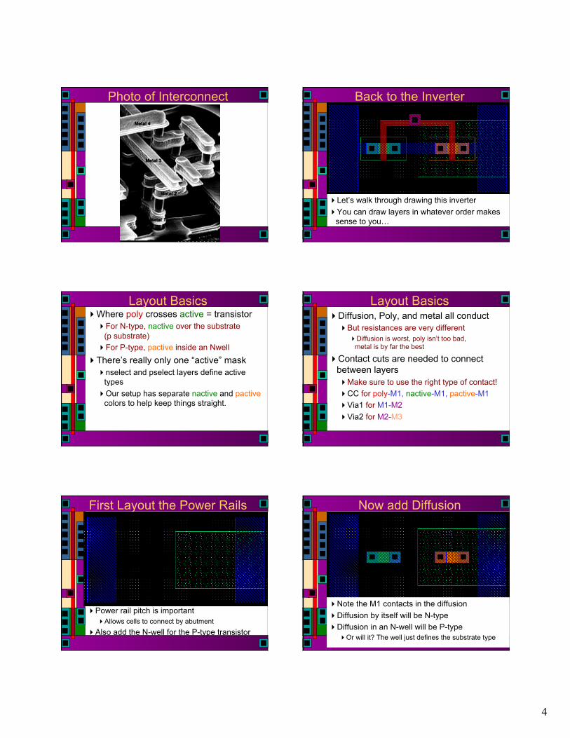
Photo of Interconnect Back to the Inverter
Let’s walk through drawing this inverter You can draw layers in whatever order makes
sense to you…
Layout Basics Where poly crosses active = transistor
For N-type, nactive over the substrate (p substrate)
For P-type, pactive inside an Nwell There’s really only one “active” mask
nselect and pselect layers define active types
Our setup has separate nactive and pactive colors to help keep things straight.
Layout Basics Diffusion, Poly, and metal all conduct
But resistances are very different Diffusion is worst, poly isn’t too bad,
metal is by far the best
Contact cuts are needed to connect between layers Make sure to use the right type of contact! CC for poly-M1, nactive-M1, pactive-M1 Via1 for M1-M2 Via2 for M2-M3
First Layout the Power Rails
Power rail pitch is important Allows cells to connect by abutment
Also add the N-well for the P-type transistor
Now add Diffusion
Note the M1 contacts in the diffusion Diffusion by itself will be N-type Diffusion in an N-well will be P-type
Or will it? The well just defines the substrate type

5
Add the Select Regions
Nselect defines N-type diffusion Pselect defines P-type diffusion
Now add the Poly Gates
Remember: crossing diffusion with Poly makes a transistor The type of the diffusion, and the type of well, define
what kind of transistor
Note the Metal1 Connections
Overlapping boxes of the same type of material make a connection
Overlaps of different types of material need a contact cut of some sort
Connect the Gates
Connect gates together to form the inverter Note contact cuts and metal overlaps
Layout Subtlety We currently think of transistors as three-
terminal devices Gate, Source, Drain
They’re really four-terminal devices There’s also a connection to the substrate
It’s important to tie the substrate to a specific voltage GND for the P-substrate VDD for the N-well
Make sure PN-diodes from active to substrate and well are reverse-biased…
Well (or Substrate) Contacts
Connect P-substrate to GND (VSS) with a little stub of P-type diffusion (remember pselect)
Connect the N-well to VDD with a little stub of N-type diffusion I.e. inside the N-well, but with nselect

6
Layout Design Rules Define the allowed geometry of the
different layers Guidelines for making safe process masks Rules about the allowed sizes and shapes of
a particular layer Rules about how different layers interact
Dimensions listed in one of two ways Absolute dimensions (I.e. microns) Scalable dimensions in abstract units
Usually called “lambda” Design in lambda units, then scale lambda for a
particular process
Intra-Layer Rules (Lambda)
12
18 0 Well
Active 3
3
Polysilicon 3 2
Different Potential Same Potential
Metal1 3
3
2
Contact or Via
Select 2
or 6
2 Hole
Metal2 3 3
Metal3 4 5
2
Lambda = 0.50 => 1.0u process Lambda = 0.30 => 0.6u process
Intra-Layer Rules (Native)
5
5 0 Well
Active 0.8
0.8
Polysilicon 0.6 0.6
Different Potential Same Potential
Metal1 0.6
0.6
0.5
Contact or Via
Select 1
or 5
0.5 Hole
Metal2 0.7 0.7
Metal3 0.7 0.8
1
Dimensions are directly in microns Some things scale uniformly, others don’t Native rules are generally more dense
Transistor Layout Measurements are in microns based on scalable rules and a lambda of 0.3.
Vias and Contacts Look at Inverter Layout Again
Lots and lots of design rules to consider! Use Design Rule Checking (DRC) to see if
everything is OK

7
Layout Design Rules On the class web page Modified version of the MOSIS SCMOS
Rev. 8 rules Modified to show both Lambda and Micron
dimensions All our design will be done in microns
Because of the NCSU tech files
But, even though we’re using microns, we’re using the SCMOS Lambda rules…
Print them out in color if possible!
SCMOS Nwell
SCMOS Active (diffusion) SCMOS Poly
SCMOS Select SCMOS Contacts

8
SCMOS Contact to Poly SCMOS Contact to Active
SCMOS Metal1 SCMOS Via
SCMOS Metal2 SCMOS Via2
9
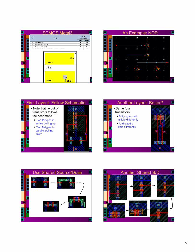
SCMOS Metal3 An Example: NOR
NOR schematic in Composer
First Layout: Follow Schematic Note that layout of
transistors follows the schematic Two P-types in
series pulling up Two N-types in
parallel pulling down
Another Layout: Better? Same four
transistors But, organized
a little differently And sized a
little differently
Use Shared Source/Drain Another Shared S/D

10
Two NOR Gates Transistor Sizing We’ll get into the details later… Consider a transistor’s Width and Length
Current capability is proportional to W/L Length is almost always minimum allowed Change width to change current capability
Sizing Rule of Thumb Also, P-type is about twice as bad as
N-type Has to do with hole mobility vs. electron
mobility So, make P-types twice as wide as
N-types to start with Unit size for transistors this semester
N-type 1.5µ (contact pitch is 1.2µ) P-type 3µ
Sizing Rule of Thumb Now multiply each width by n for a series
stack of n transistors. Stack of 2 in series, each transistor should
be 2x unit size Stack of 3 in series, each transistor should
be 3x unit size
This is because series connections are like increasing the L of the device… Current is proportional to W/L
For example: Notice the
difference in width…
This roughly equalizes the current sourcing capability of pull-up and pull-down stacks in this gate
Related Documents