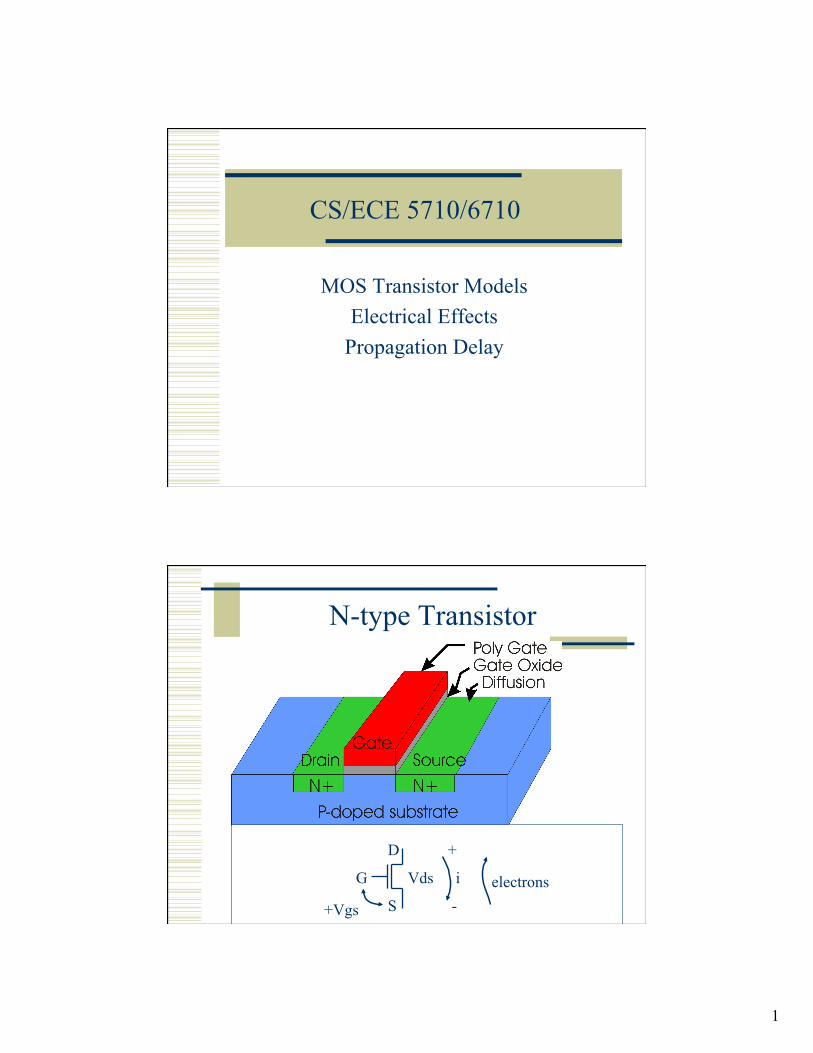
1 CS/ECE 5710/6710 MOS Transistor Models Electrical Effects Propagation Delay N-type Transistor + - i electrons Vds +Vgs S G D

Welcome message from author
This document is posted to help you gain knowledge. Please leave a comment to let me know what you think about it! Share it to your friends and learn new things together.
Transcript
1
CS/ECE 5710/6710
MOS Transistor Models Electrical Effects
Propagation Delay
N-type Transistor
+
-
i electrons Vds
+Vgs S
G
D
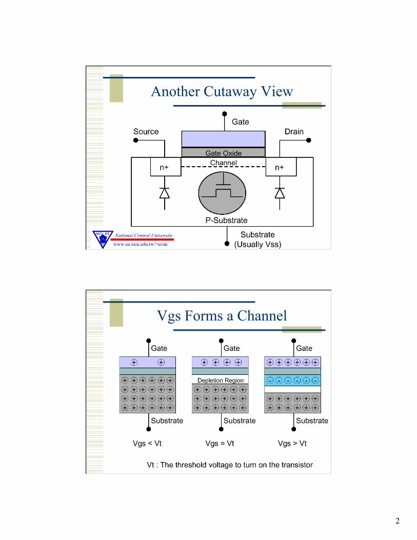
2
Another Cutaway View
Vgs Forms a Channel
3
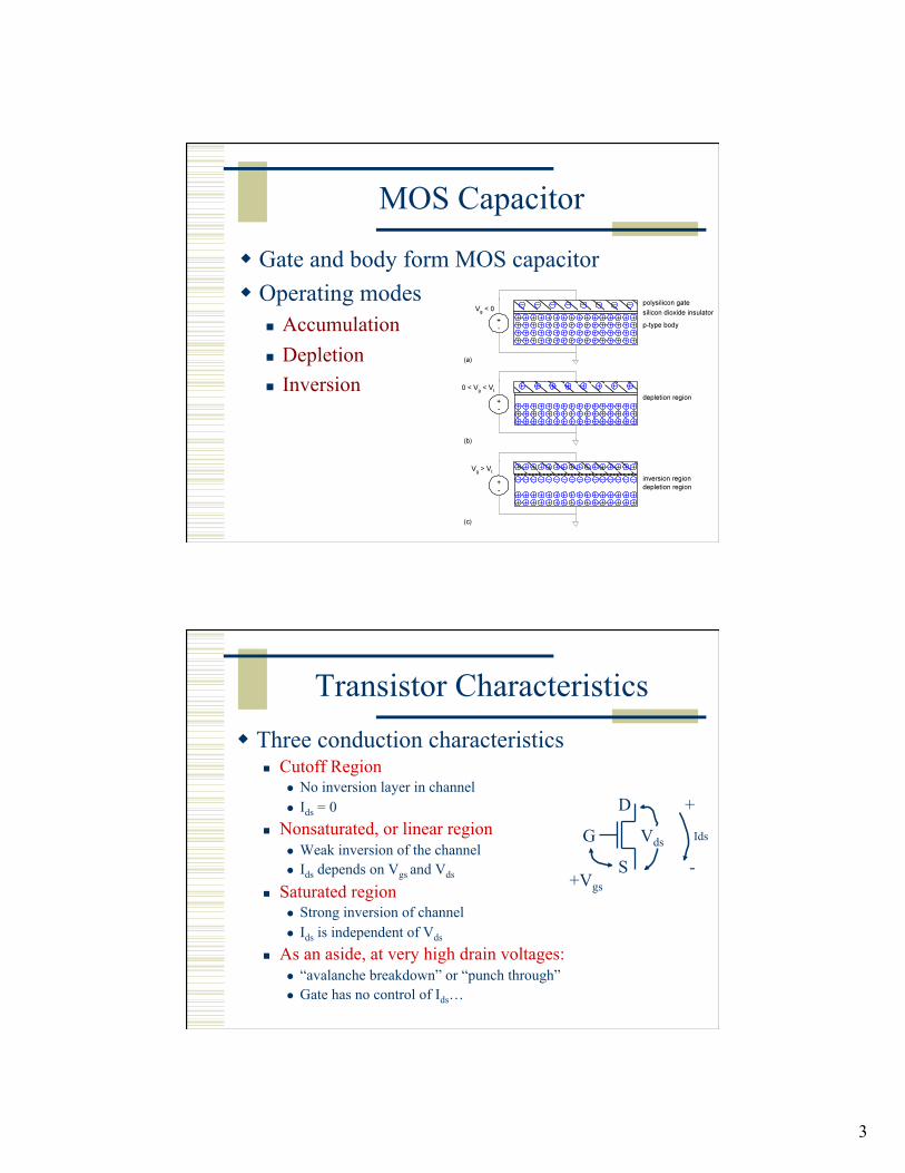
MOS Capacitor
Gate and body form MOS capacitor Operating modes
Accumulation Depletion Inversion
Transistor Characteristics Three conduction characteristics
Cutoff Region No inversion layer in channel Ids = 0
Nonsaturated, or linear region Weak inversion of the channel Ids depends on Vgs and Vds
Saturated region Strong inversion of channel Ids is independent of Vds
As an aside, at very high drain voltages: “avalanche breakdown” or “punch through” Gate has no control of Ids…
+
-
Ids Vds
+Vgs S
G
D
4
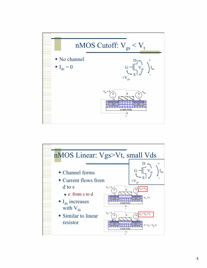
nMOS Cutoff: Vgs < Vt
No channel Ids = 0
+
-
Ids Vds
+Vgs S
G
D
nMOS Linear: Vgs>Vt, small Vds
Channel forms Current flows from
d to s e- from s to d
Ids increases with Vds
Similar to linear resistor
+
-
Ids Vds
+Vgs S
G
D
5
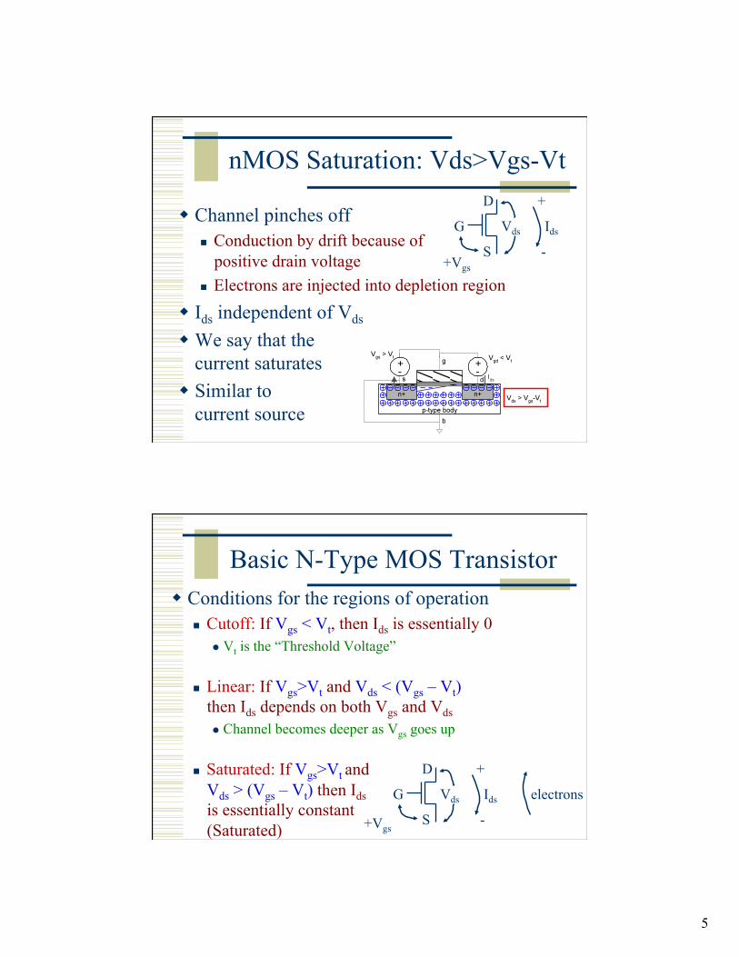
nMOS Saturation: Vds>Vgs-Vt
Channel pinches off Conduction by drift because of
positive drain voltage Electrons are injected into depletion region
Ids independent of Vds
We say that the current saturates
Similar to current source
+
-
Ids Vds
+Vgs S
G
D
Basic N-Type MOS Transistor Conditions for the regions of operation
Cutoff: If Vgs < Vt, then Ids is essentially 0 Vt is the “Threshold Voltage”
Linear: If Vgs>Vt and Vds < (Vgs – Vt) then Ids depends on both Vgs and Vds Channel becomes deeper as Vgs goes up
Saturated: If Vgs>Vt and Vds > (Vgs – Vt) then Ids is essentially constant (Saturated)
+
-
Ids electrons Vds
+Vgs S
G
D
6
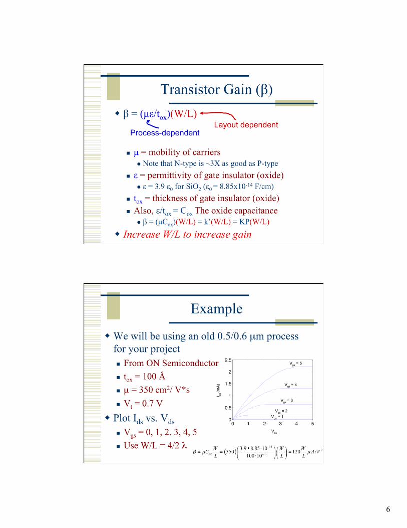
Transistor Gain (β) β = (µε/tox)(W/L)
µ = mobility of carriers Note that N-type is ~3X as good as P-type
ε = permittivity of gate insulator (oxide) ε = 3.9 ε0 for SiO2 (ε0 = 8.85x10⁻¹⁴ F/cm)
tox = thickness of gate insulator (oxide) Also, ε/tox = Cox The oxide capacitance
β = (µCox)(W/L) = k’(W/L) = KP(W/L)
Increase W/L to increase gain
Process-dependent Layout dependent
Example
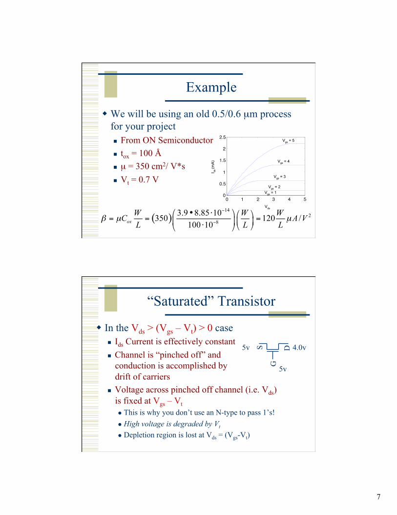
We will be using an old 0.5/0.6 µm process for your project From ON Semiconductor tox = 100 Å µ = 350 cm2/ V*s Vt = 0.7 V
Plot Ids vs. Vds Vgs = 0, 1, 2, 3, 4, 5 Use W/L = 4/2 λ
7
Example
We will be using an old 0.5/0.6 µm process for your project From ON Semiconductor tox = 100 Å µ = 350 cm2/ V*s Vt = 0.7 V
“Saturated” Transistor
In the Vds > (Vgs – Vt) > 0 case Ids Current is effectively constant Channel is “pinched off” and
conduction is accomplished by drift of carriers
Voltage across pinched off channel (i.e. Vds) is fixed at Vgs – Vt This is why you don’t use an N-type to pass 1’s! High voltage is degraded by Vt
Depletion region is lost at Vds = (Vgs-Vt)
S
G
D
5v
5v 4.0v
8
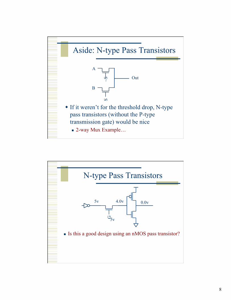
Aside: N-type Pass Transistors
If it weren’t for the threshold drop, N-type pass transistors (without the P-type transmission gate) would be nice 2-way Mux Example…
~S
S
A
B
Out
N-type Pass Transistors
Is this a good design using an nMOS pass transistor?
G
5v
5v 4.0v 0.0v
9
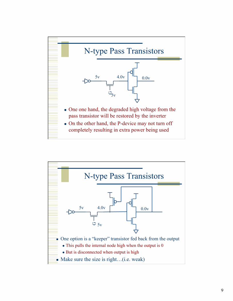
N-type Pass Transistors
One one hand, the degraded high voltage from the pass transistor will be restored by the inverter
On the other hand, the P-device may not turn off completely resulting in extra power being used
G
5v
5v 4.0v 0.0v
N-type Pass Transistors
One option is a “keeper” transistor fed back from the output This pulls the internal node high when the output is 0 But is disconnected when output is high
Make sure the size is right…(i.e. weak)
G
5v
5v 4.0v 0.0v
10
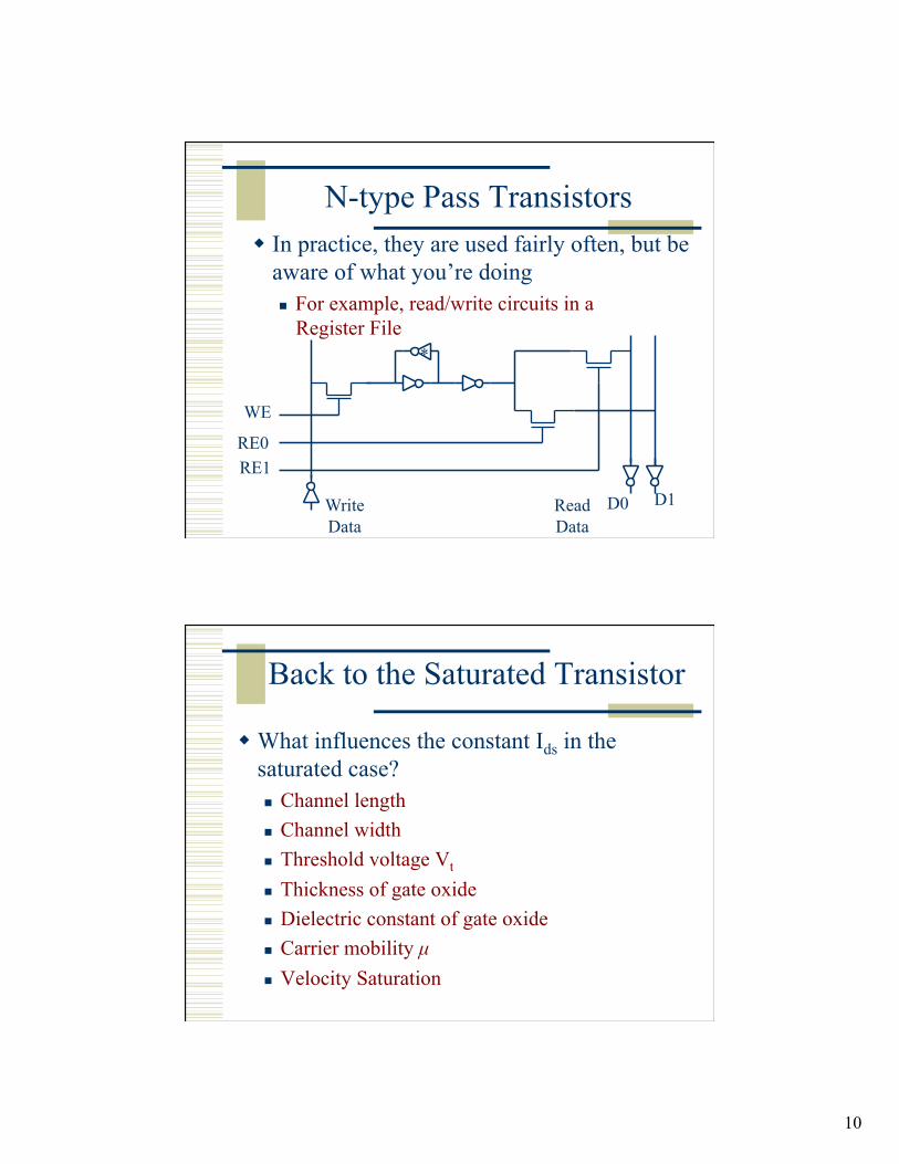
N-type Pass Transistors In practice, they are used fairly often, but be
aware of what you’re doing For example, read/write circuits in a
Register File *
Write Data
Read Data
WE
RE0 RE1
D0 D1
Back to the Saturated Transistor
What influences the constant Ids in the saturated case? Channel length Channel width Threshold voltage Vt
Thickness of gate oxide Dielectric constant of gate oxide Carrier mobility µ Velocity Saturation

11
Back to the Saturated Transistor
What influences the constant Ids in the saturated case? Channel length Channel width Threshold voltage Vt
Thickness of gate oxide Dielectric constant of gate oxide Carrier mobility µ Velocity Saturation
Threshold Voltage: Vt
The Vgs voltage at which Ids is essentially 0 Vt = .67v for nmos and -.92v for pmos in our process Tiny Ids is exponentially related to Vgs, Vds
Take 6770 & 6720 for “subthreshold” circuit ideas Vt is affected by
Gate conductor material Gate insulator material Gate insulator thickness Channel doping Impurities at Si/insulator interface Voltage between source and substrate (Vsb)
12
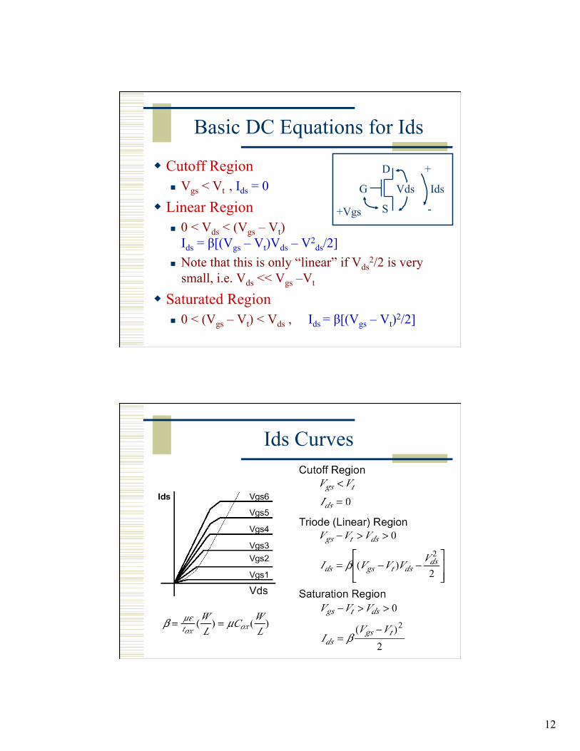
Basic DC Equations for Ids
Cutoff Region Vgs < Vt , Ids = 0
Linear Region 0 < Vds < (Vgs – Vt)
Ids = β[(Vgs – Vt)Vds – V2ds/2]
Note that this is only “linear” if Vds2/2 is very
small, i.e. Vds << Vgs –Vt
Saturated Region 0 < (Vgs – Vt) < Vds , Ids = β[(Vgs – Vt)2/2]
+
-
Ids Vds
+Vgs S
G
D
Ids Curves
13
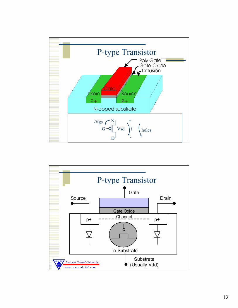
P-type Transistor
+
-
i holes Vsd -Vgs S
G
D
P-type Transistor
14
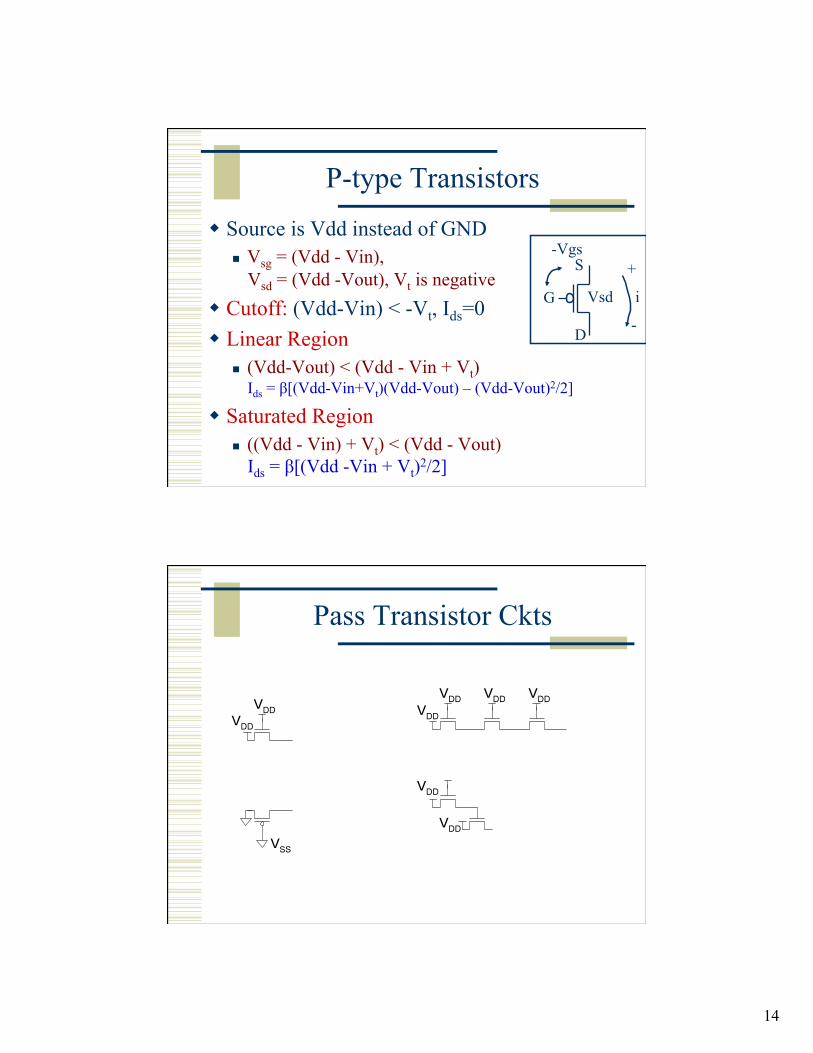
P-type Transistors
Source is Vdd instead of GND Vsg = (Vdd - Vin),
Vsd = (Vdd -Vout), Vt is negative Cutoff: (Vdd-Vin) < -Vt, Ids=0 Linear Region
(Vdd-Vout) < (Vdd - Vin + Vt) Ids = β[(Vdd-Vin+Vt)(Vdd-Vout) – (Vdd-Vout)2/2]
Saturated Region ((Vdd - Vin) + Vt) < (Vdd - Vout)
Ids = β[(Vdd -Vin + Vt)2/2]
+
-
i Vsd
-Vgs S
G
D
Pass Transistor Ckts
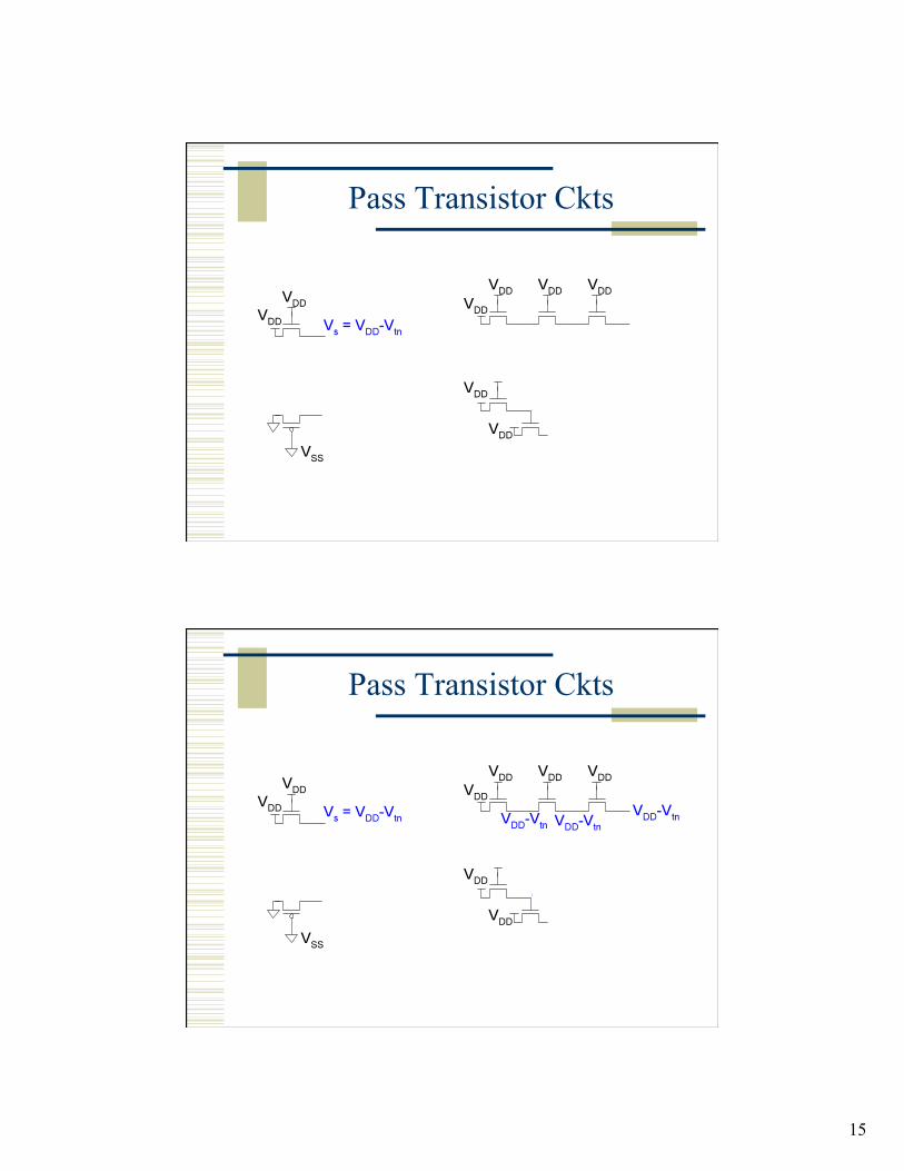
15
Pass Transistor Ckts
Pass Transistor Ckts
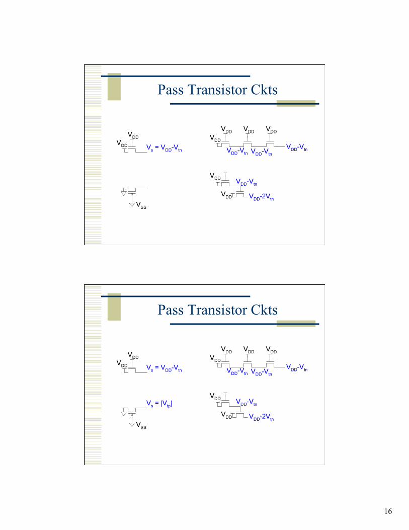
16
Pass Transistor Ckts
Pass Transistor Ckts
17
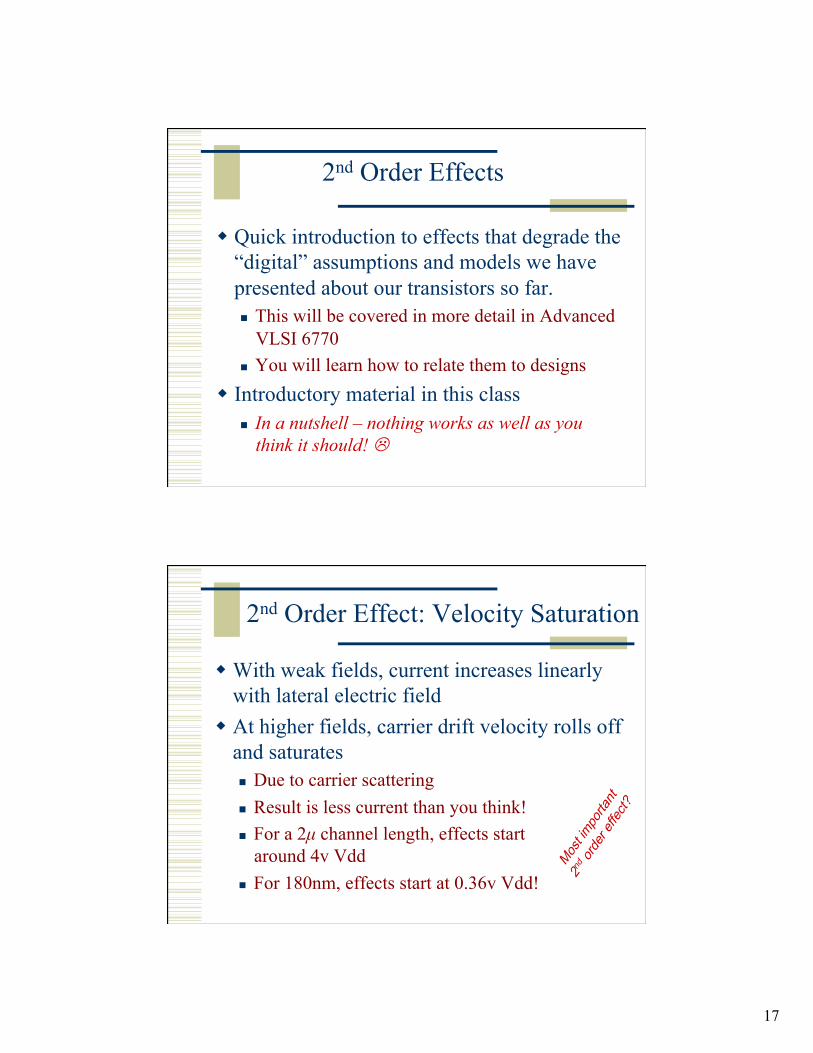
2nd Order Effects
Quick introduction to effects that degrade the “digital” assumptions and models we have presented about our transistors so far. This will be covered in more detail in Advanced
VLSI 6770 You will learn how to relate them to designs
Introductory material in this class In a nutshell – nothing works as well as you
think it should!
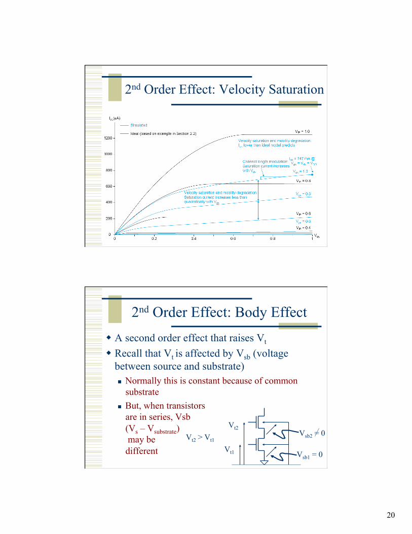
2nd Order Effect: Velocity Saturation
With weak fields, current increases linearly with lateral electric field
At higher fields, carrier drift velocity rolls off and saturates Due to carrier scattering Result is less current than you think! For a 2µ channel length, effects start
around 4v Vdd For 180nm, effects start at 0.36v Vdd!
Most im
porta
nt
2nd or
der e
ffect?
18
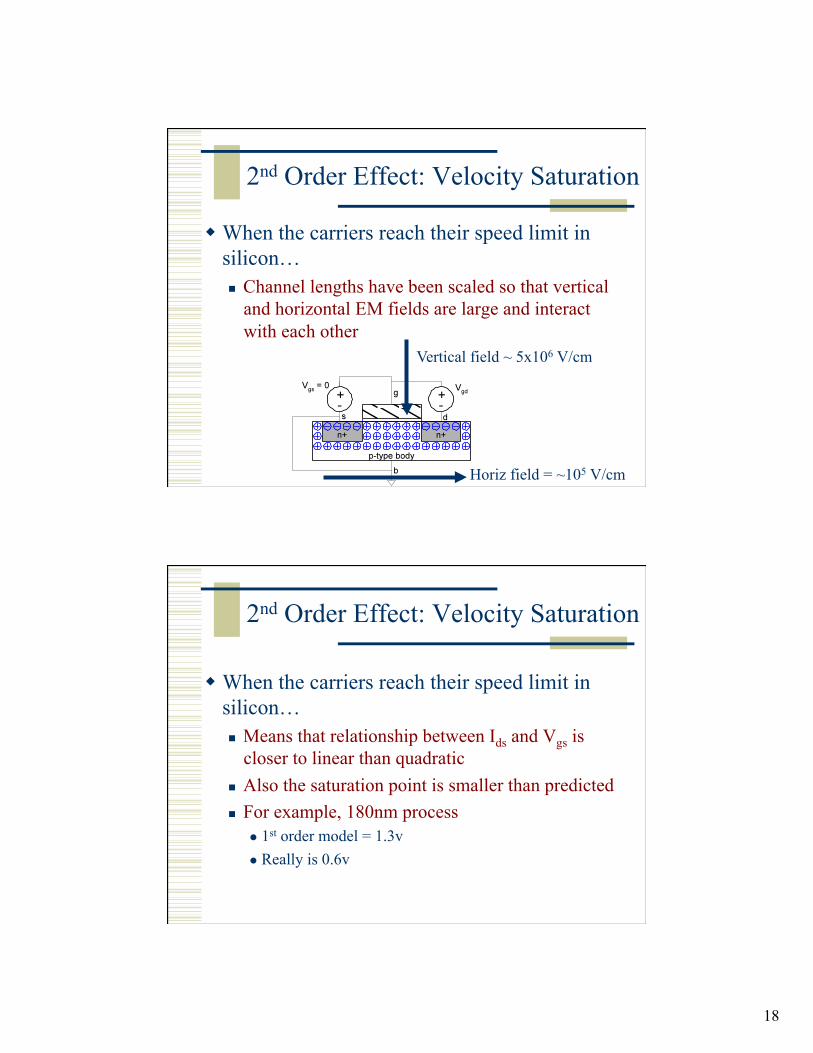
2nd Order Effect: Velocity Saturation
When the carriers reach their speed limit in silicon… Channel lengths have been scaled so that vertical
and horizontal EM fields are large and interact with each other
Vertical field ~ 5x10⁶ V/cm
Horiz field = ~105 V/cm
2nd Order Effect: Velocity Saturation
When the carriers reach their speed limit in silicon… Means that relationship between Ids and Vgs is
closer to linear than quadratic Also the saturation point is smaller than predicted For example, 180nm process
1st order model = 1.3v Really is 0.6v
19
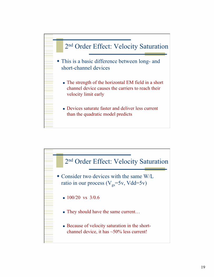
2nd Order Effect: Velocity Saturation
This is a basic difference between long- and short-channel devices
The strength of the horizontal EM field in a short channel device causes the carriers to reach their velocity limit early
Devices saturate faster and deliver less current than the quadratic model predicts
2nd Order Effect: Velocity Saturation
Consider two devices with the same W/L ratio in our process (Vgs=5v, Vdd=5v)
100/20 vs 3/0.6
They should have the same current…
Because of velocity saturation in the short-channel device, it has ~50% less current!
20
2nd Order Effect: Velocity Saturation
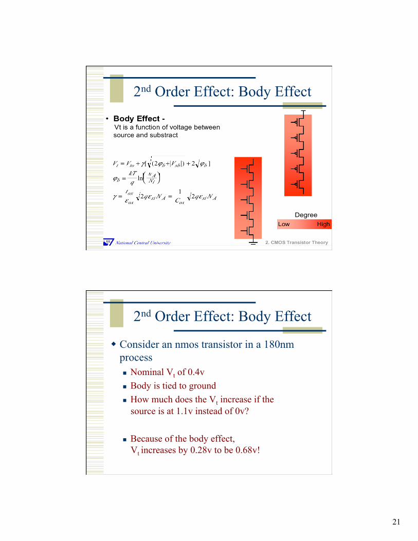
2nd Order Effect: Body Effect
A second order effect that raises Vt
Recall that Vt is affected by Vsb (voltage between source and substrate) Normally this is constant because of common
substrate But, when transistors
are in series, Vsb (Vs – Vsubstrate) may be different Vt1
Vt2
Vsb1 = 0
Vsb2 = 0 Vt2 > Vt1
21
2nd Order Effect: Body Effect
2nd Order Effect: Body Effect
Consider an nmos transistor in a 180nm process Nominal Vt of 0.4v Body is tied to ground How much does the Vt increase if the
source is at 1.1v instead of 0v?
Because of the body effect, Vt increases by 0.28v to be 0.68v!
22
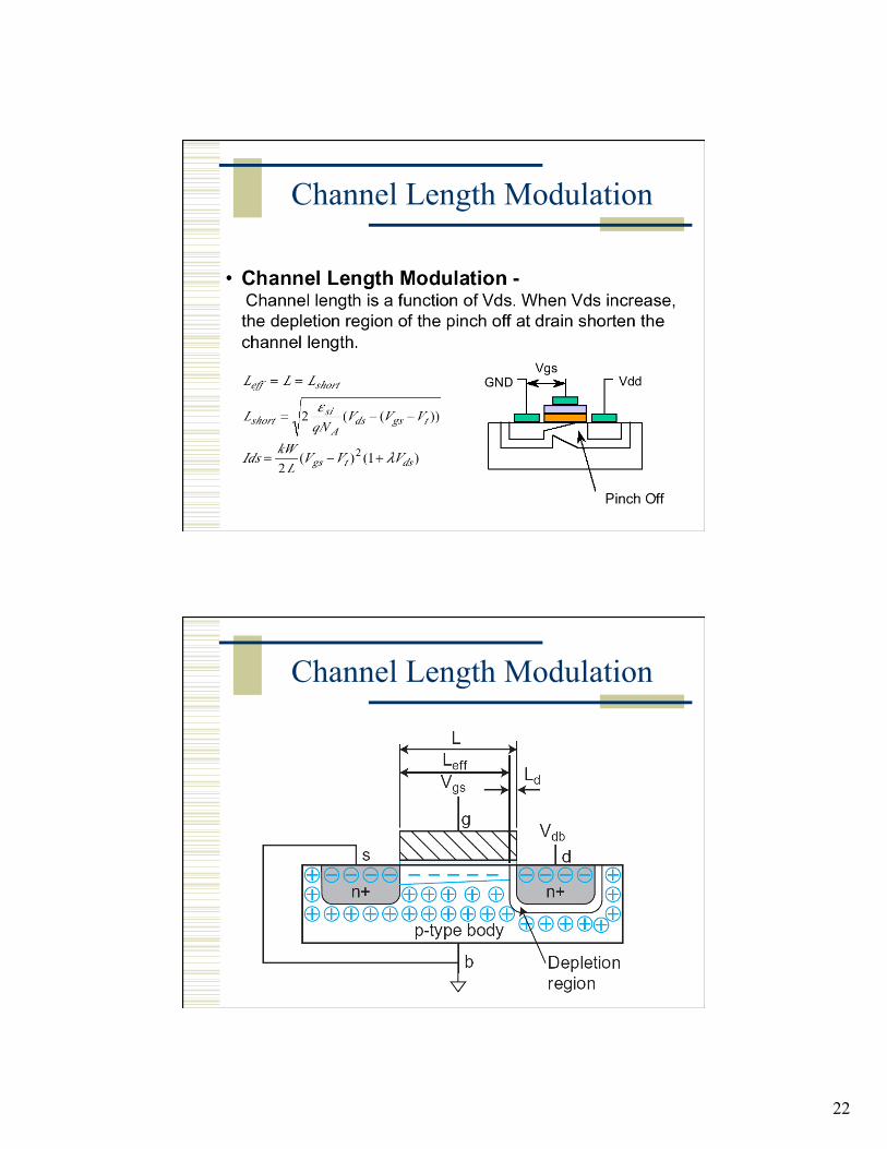
Channel Length Modulation
Channel Length Modulation
23
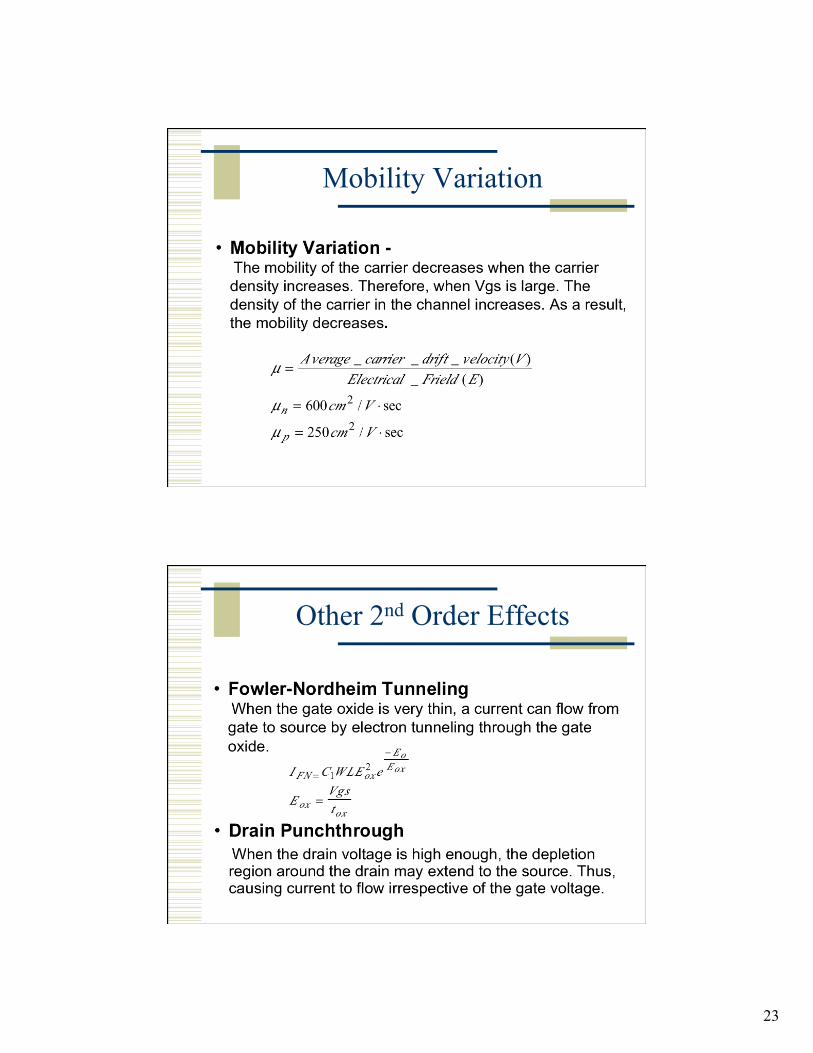
Mobility Variation
Other 2nd Order Effects
24
Other 2nd Order Effects
Inverter Switching Point
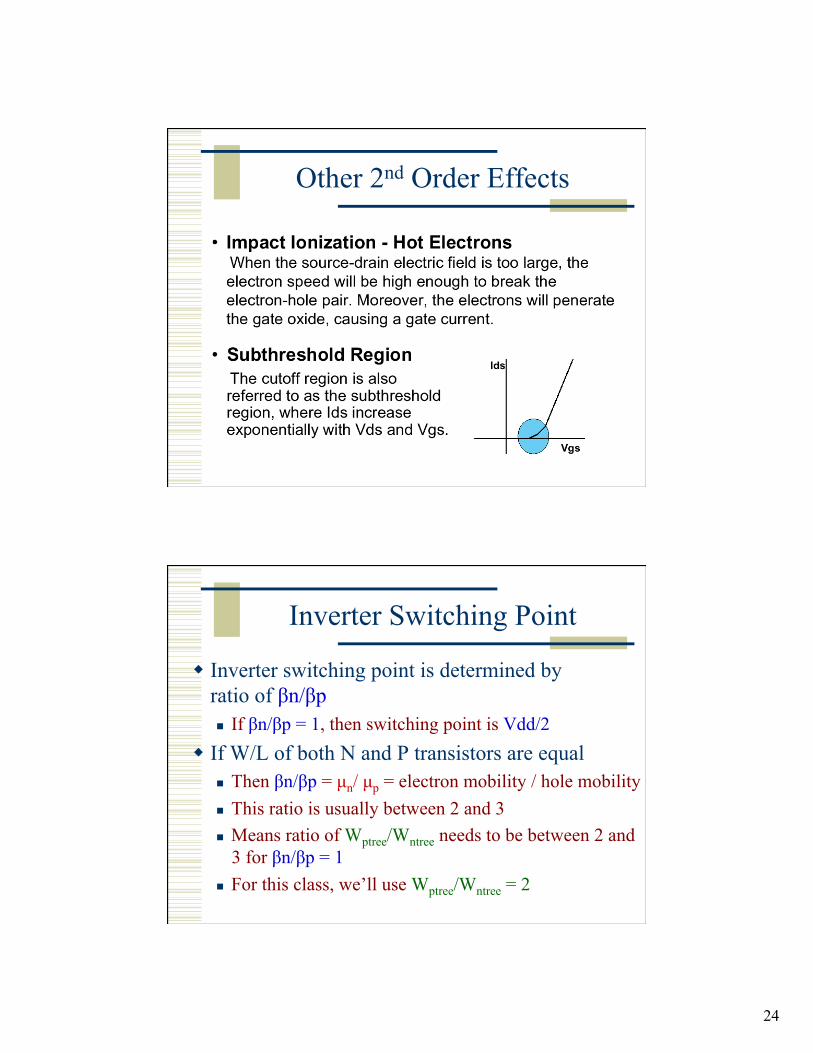
Inverter switching point is determined by ratio of βn/βp If βn/βp = 1, then switching point is Vdd/2
If W/L of both N and P transistors are equal Then βn/βp = µn/ µp = electron mobility / hole mobility This ratio is usually between 2 and 3 Means ratio of Wptree/Wntree needs to be between 2 and
3 for βn/βp = 1 For this class, we’ll use Wptree/Wntree = 2
25
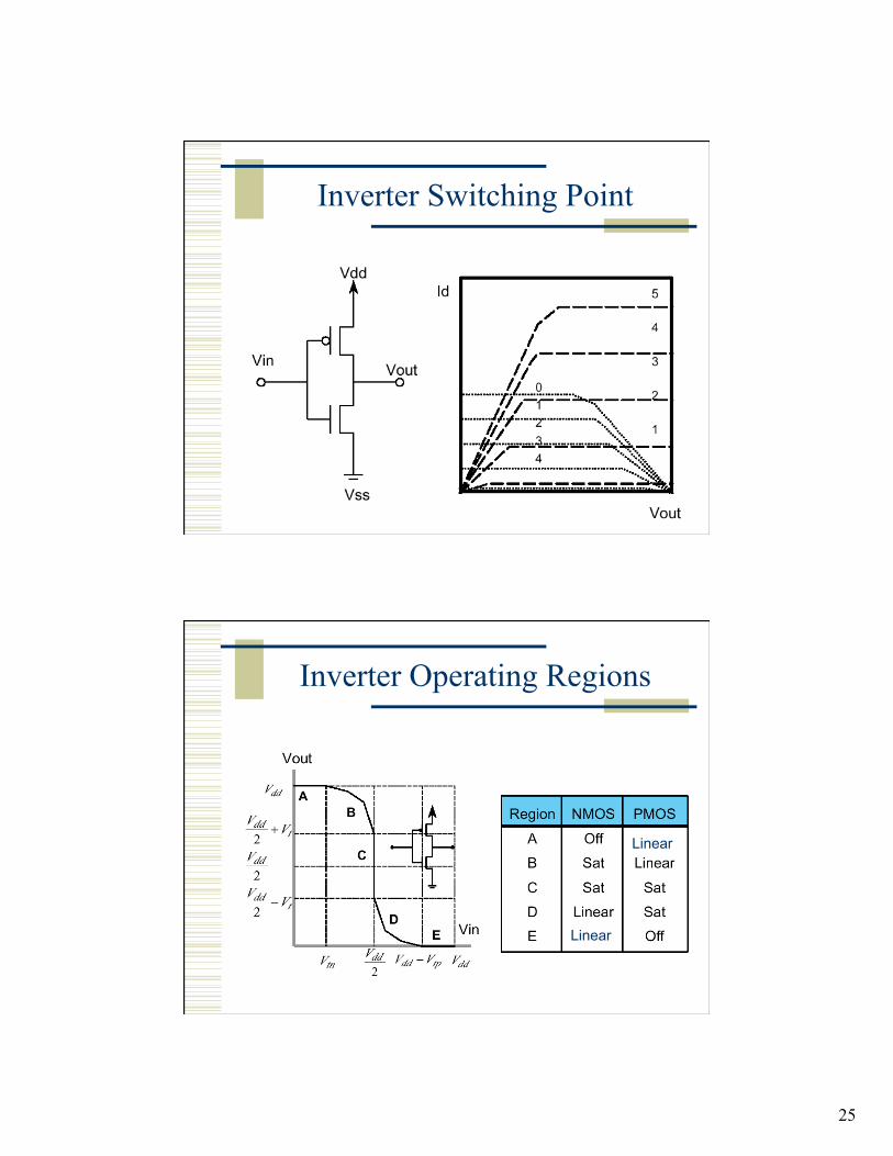
Inverter Switching Point
Inverter Operating Regions
Linear
Linear
26
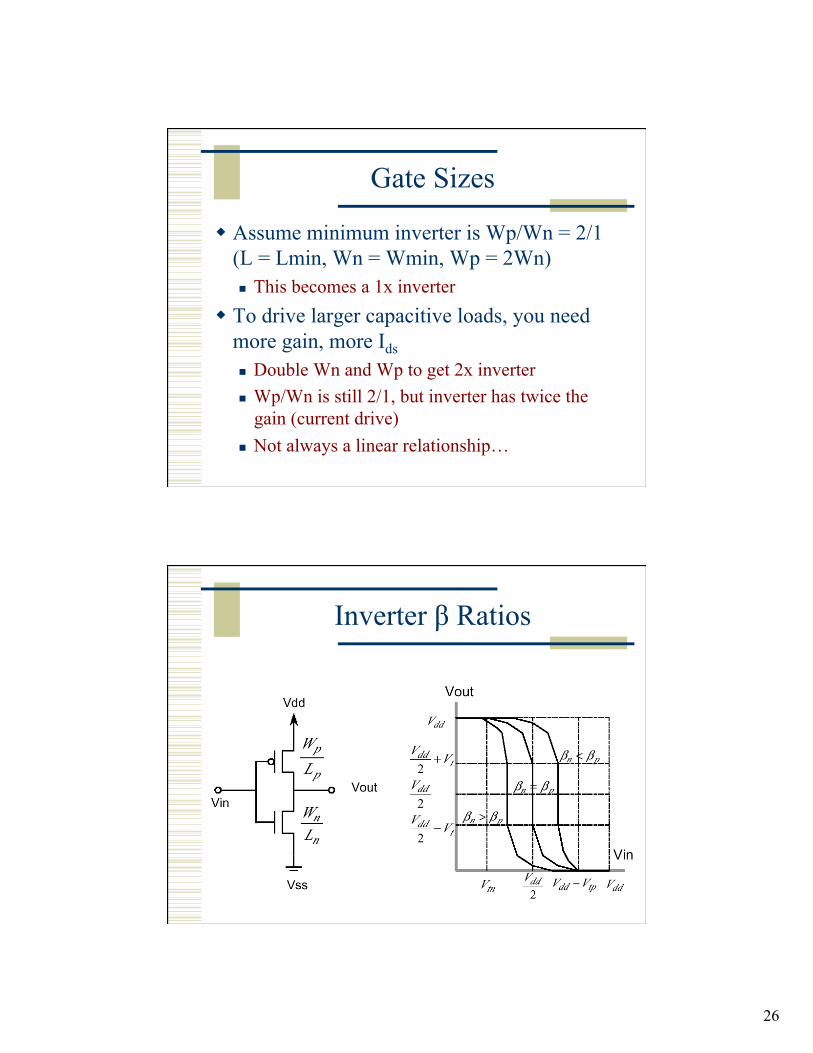
Gate Sizes
Assume minimum inverter is Wp/Wn = 2/1 (L = Lmin, Wn = Wmin, Wp = 2Wn) This becomes a 1x inverter
To drive larger capacitive loads, you need more gain, more Ids Double Wn and Wp to get 2x inverter Wp/Wn is still 2/1, but inverter has twice the
gain (current drive) Not always a linear relationship…
Inverter β Ratios
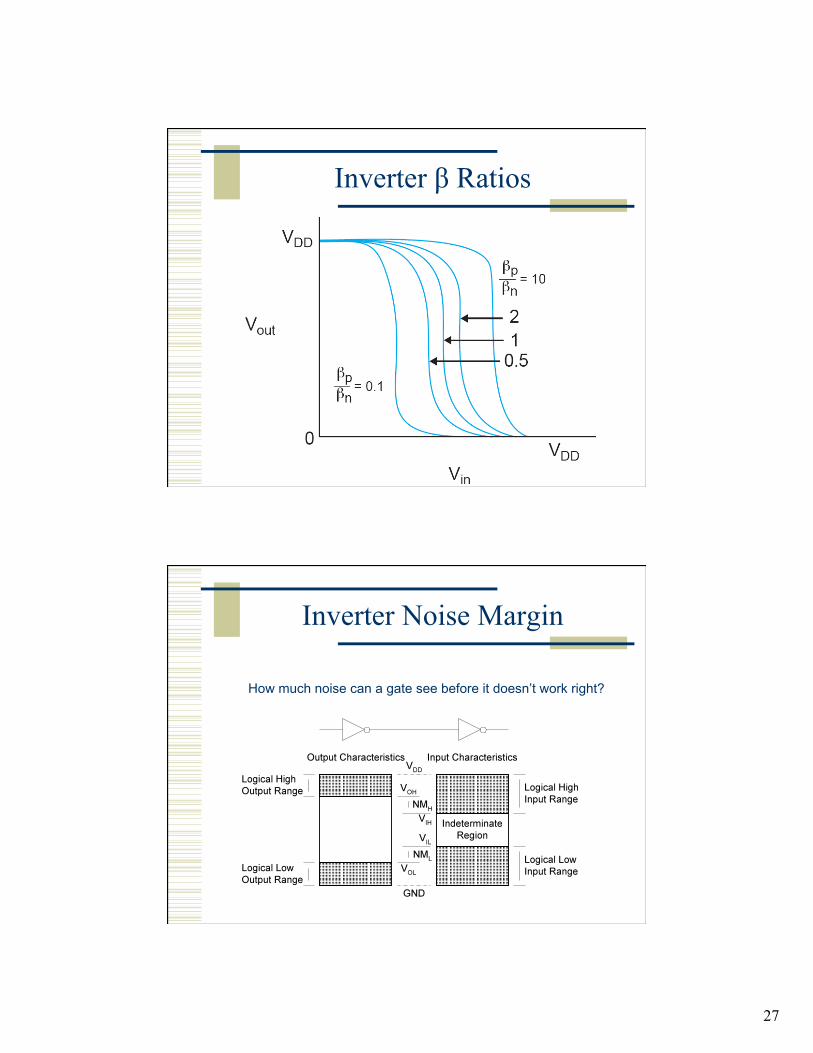
27
Inverter β Ratios
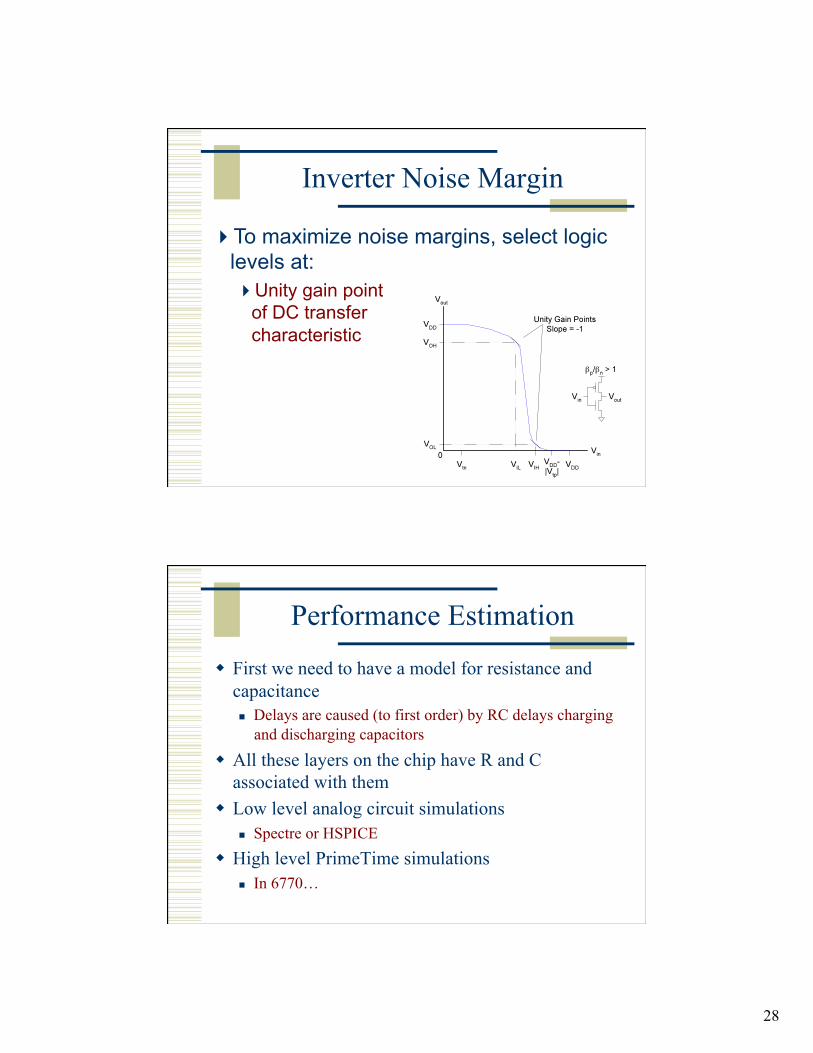
Inverter Noise Margin
How much noise can a gate see before it doesn’t work right?
28
Inverter Noise Margin
To maximize noise margins, select logic levels at: Unity gain point
of DC transfer characteristic
Performance Estimation
First we need to have a model for resistance and capacitance Delays are caused (to first order) by RC delays charging
and discharging capacitors
All these layers on the chip have R and C associated with them
Low level analog circuit simulations Spectre or HSPICE
High level PrimeTime simulations In 6770…
29
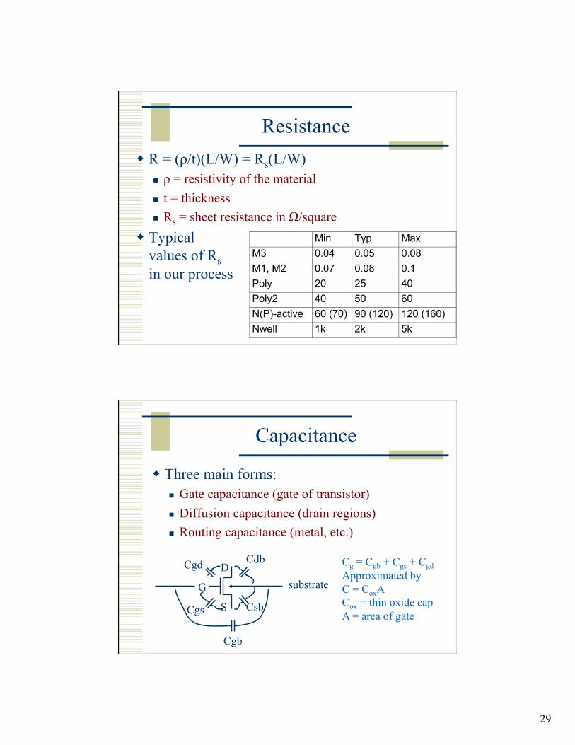
Resistance R = (ρ/t)(L/W) = Rs(L/W)
ρ = resistivity of the material t = thickness Rs = sheet resistance in Ω/square
Typical values of Rs in our process
Capacitance
Three main forms: Gate capacitance (gate of transistor) Diffusion capacitance (drain regions) Routing capacitance (metal, etc.)
S
G
D substrate
Cgd
Cgs
Cgb
Cdb
Csb
Cg = Cgb + Cgs + Cgd Approximated by C = CoxA Cox = thin oxide cap A = area of gate
30
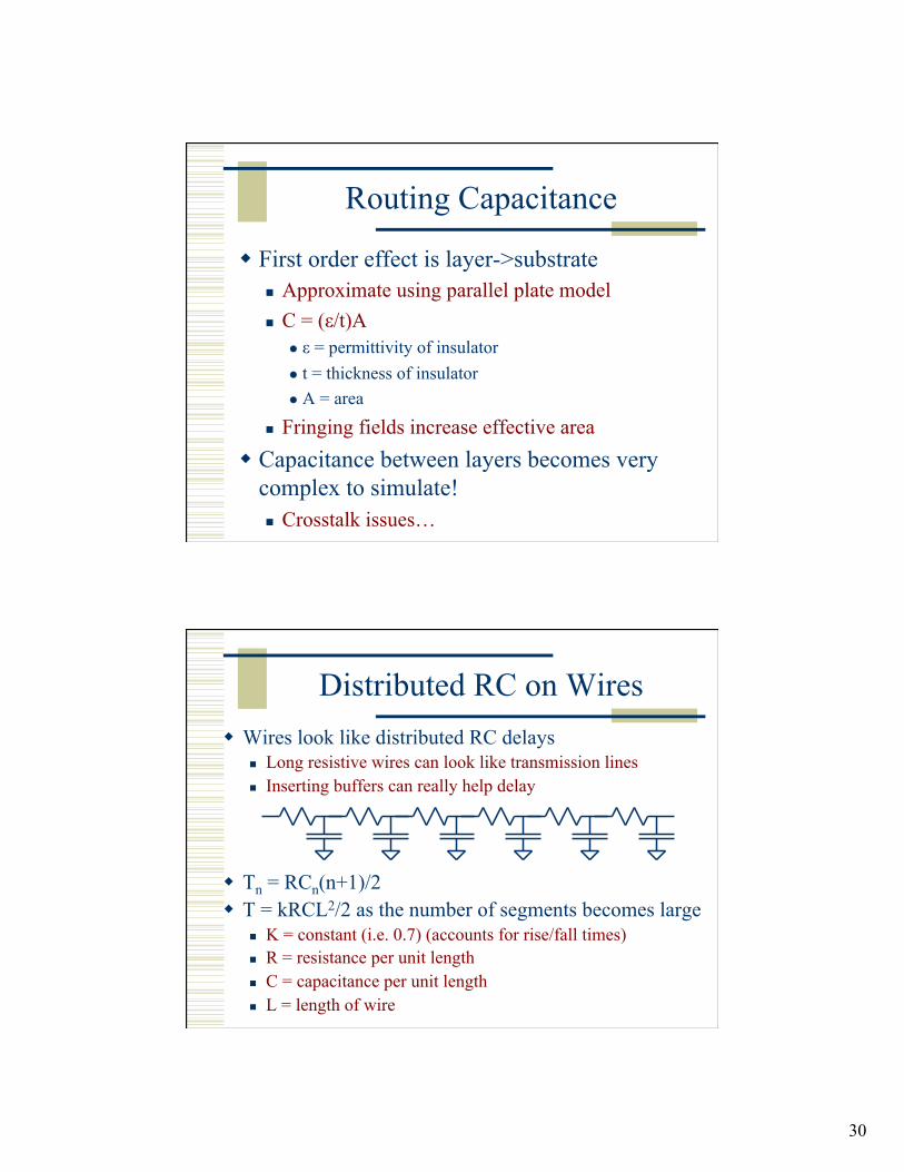
Routing Capacitance
First order effect is layer->substrate Approximate using parallel plate model C = (ε/t)A
ε = permittivity of insulator t = thickness of insulator A = area
Fringing fields increase effective area Capacitance between layers becomes very
complex to simulate! Crosstalk issues…
Distributed RC on Wires Wires look like distributed RC delays
Long resistive wires can look like transmission lines Inserting buffers can really help delay
Tn = RCn(n+1)/2 T = kRCL2/2 as the number of segments becomes large
K = constant (i.e. 0.7) (accounts for rise/fall times) R = resistance per unit length C = capacitance per unit length L = length of wire

31
RC Wire Delay Example
R = 20Ω/sq C = 4 x 10⁻⁴ pF/um L = 2mm K = 0.7 T = kRCL2/2 T = (0.7) (20) (4 x 10-15)(2000)2 / 2 s
delay = 11.2 ns
RC Wire/Buffer Delay Example
Now split into 2 segments of 1mm with a buffer
T = 2 x (0.7)(20)(4x10-15)(1000)2)/2+ Tbuf = 5.6ns + Tbuf
Assuming Tbuf is less than 5.6ns (which it will be), the split wire is a win
32
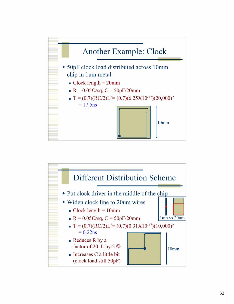
Another Example: Clock
50pF clock load distributed across 10mm chip in 1um metal Clock length = 20mm R = 0.05Ω/sq, C = 50pF/20mm T = (0.7)(RC/2)L2= (0.7)(6.25X10⁻¹⁷)(20,000)2
= 17.5ns
10mm
Different Distribution Scheme
Put clock driver in the middle of the chip Widen clock line to 20um wires
Clock length = 10mm R = 0.05Ω/sq, C = 50pF/20mm T = (0.7)(RC/2)L2= (0.7)(0.31X10⁻¹⁷)(10,000)2
= 0.22ns Reduces R by a
factor of 20, L by 2 Increases C a little bit
(clock load still 50pF)
10mm
1um vs 20um
33
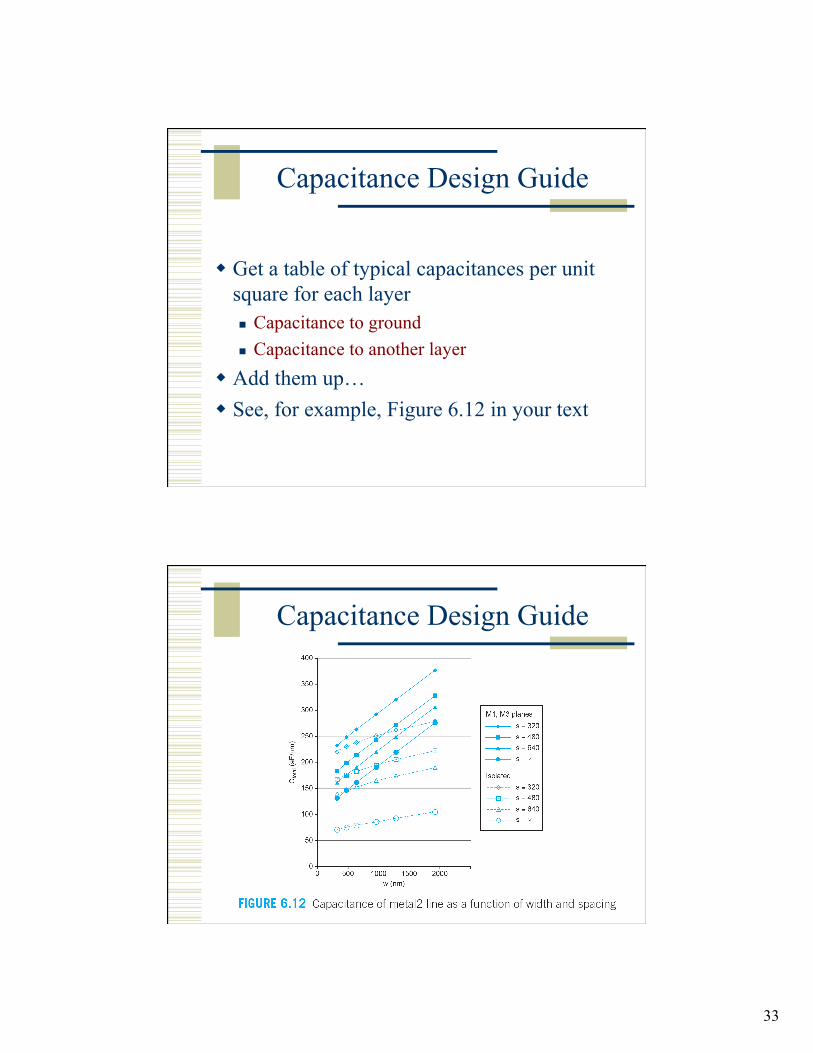
Capacitance Design Guide
Get a table of typical capacitances per unit square for each layer Capacitance to ground Capacitance to another layer
Add them up… See, for example, Figure 6.12 in your text
Capacitance Design Guide
34
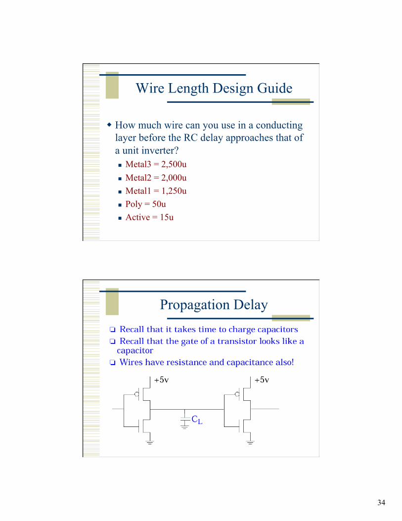
Wire Length Design Guide
How much wire can you use in a conducting layer before the RC delay approaches that of a unit inverter? Metal3 = 2,500u Metal2 = 2,000u Metal1 = 1,250u Poly = 50u Active = 15u
Propagation Delay
35
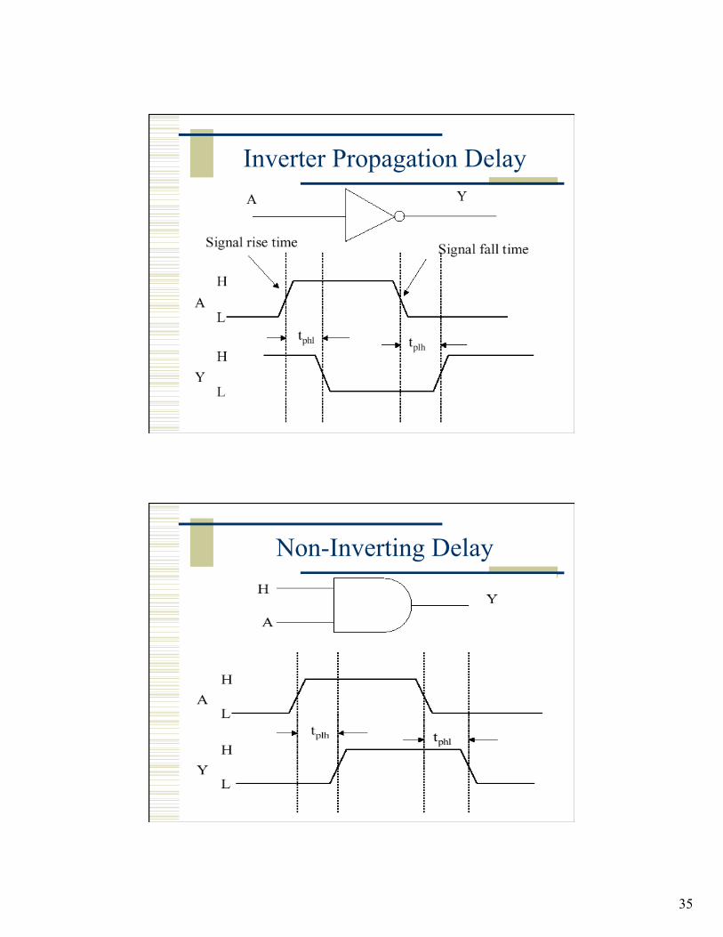
Inverter Propagation Delay
Non-Inverting Delay
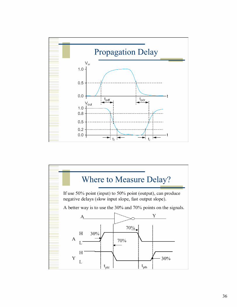
36
Propagation Delay
Where to Measure Delay?
37
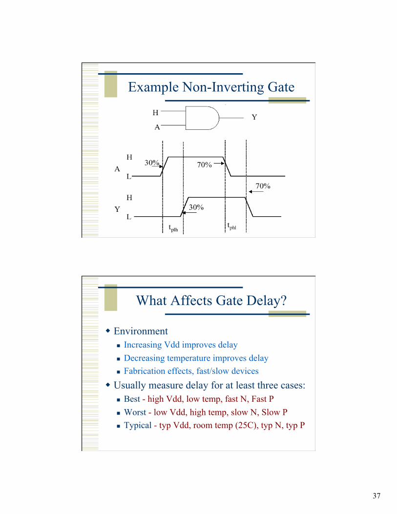
Example Non-Inverting Gate
What Affects Gate Delay?
Environment Increasing Vdd improves delay Decreasing temperature improves delay Fabrication effects, fast/slow devices
Usually measure delay for at least three cases: Best - high Vdd, low temp, fast N, Fast P Worst - low Vdd, high temp, slow N, Slow P Typical - typ Vdd, room temp (25C), typ N, typ P
38
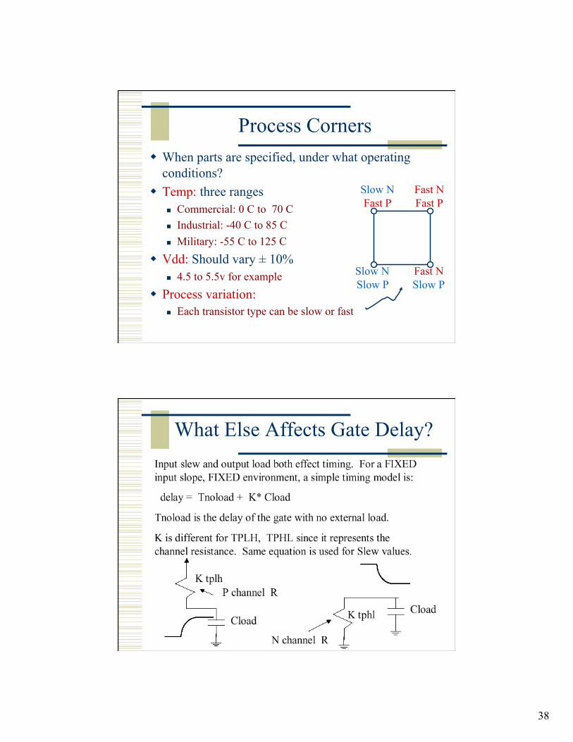
Process Corners When parts are specified, under what operating
conditions? Temp: three ranges
Commercial: 0 C to 70 C Industrial: -40 C to 85 C Military: -55 C to 125 C
Vdd: Should vary ± 10% 4.5 to 5.5v for example
Process variation: Each transistor type can be slow or fast
Slow N Slow P
Fast N Slow P
Slow N Fast P
Fast N Fast P
What Else Affects Gate Delay?
39
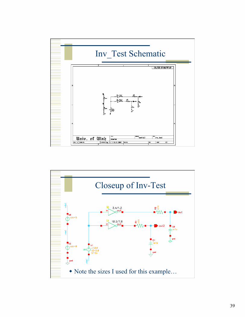
Inv_Test Schematic
Closeup of Inv-Test
Note the sizes I used for this example…
40
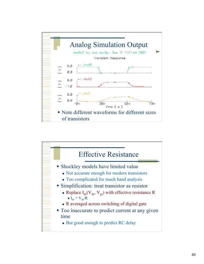
Analog Simulation Output
Note different waveforms for different sizes of transistors
Effective Resistance Shockley models have limited value
Not accurate enough for modern transistors Too complicated for much hand analysis
Simplification: treat transistor as resistor Replace Ids(Vds, Vgs) with effective resistance R
Ids = Vds/R R averaged across switching of digital gate
Too inaccurate to predict current at any given time But good enough to predict RC delay
41
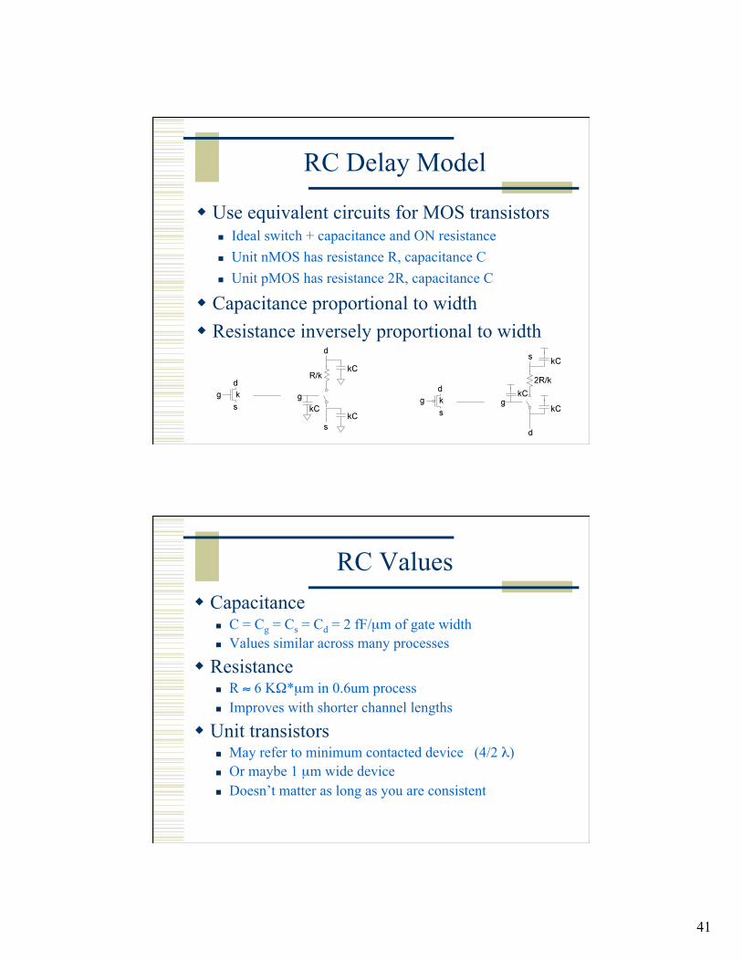
RC Delay Model
Use equivalent circuits for MOS transistors Ideal switch + capacitance and ON resistance Unit nMOS has resistance R, capacitance C Unit pMOS has resistance 2R, capacitance C
Capacitance proportional to width Resistance inversely proportional to width
RC Values Capacitance
C = Cg = Cs = Cd = 2 fF/µm of gate width Values similar across many processes
Resistance R ≈ 6 KΩ*µm in 0.6um process Improves with shorter channel lengths
Unit transistors May refer to minimum contacted device (4/2 λ) Or maybe 1 µm wide device Doesn’t matter as long as you are consistent
42
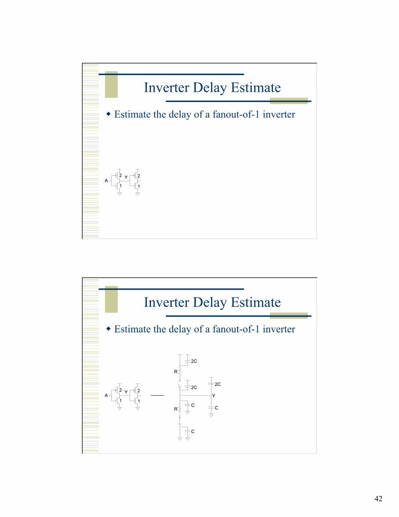
Inverter Delay Estimate
Estimate the delay of a fanout-of-1 inverter
Inverter Delay Estimate
Estimate the delay of a fanout-of-1 inverter
43
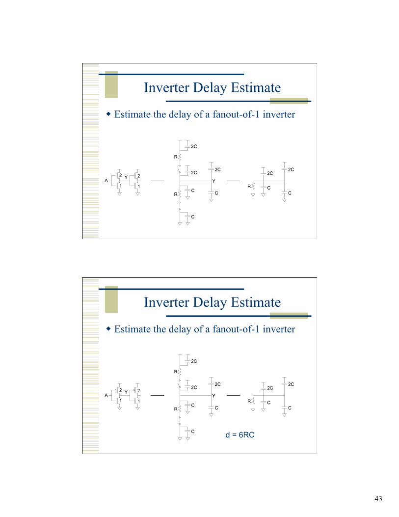
Inverter Delay Estimate
Estimate the delay of a fanout-of-1 inverter
Inverter Delay Estimate
Estimate the delay of a fanout-of-1 inverter
d = 6RC
44
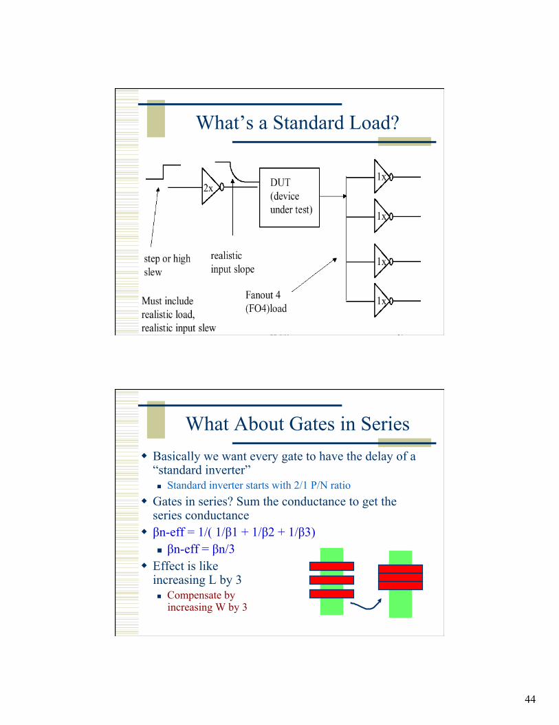
What’s a Standard Load?
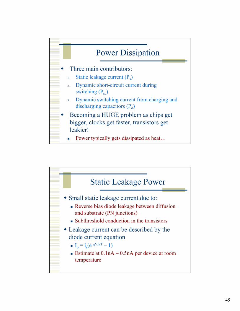
What About Gates in Series Basically we want every gate to have the delay of a
“standard inverter” Standard inverter starts with 2/1 P/N ratio
Gates in series? Sum the conductance to get the series conductance
βn-eff = 1/( 1/β1 + 1/β2 + 1/β3) βn-eff = βn/3
Effect is like increasing L by 3 Compensate by
increasing W by 3
45
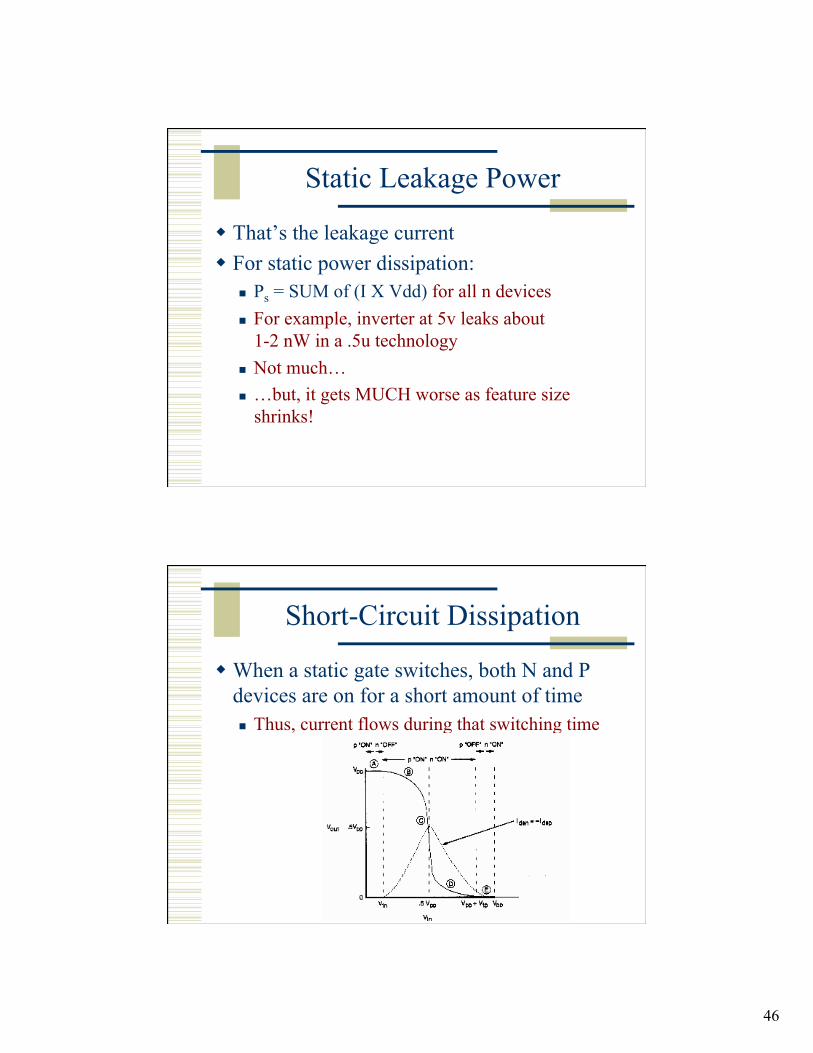
Power Dissipation
Three main contributors: 1. Static leakage current (Ps) 2. Dynamic short-circuit current during
switching (Psc) 3. Dynamic switching current from charging and
discharging capacitors (Pd) Becoming a HUGE problem as chips get
bigger, clocks get faster, transistors get leakier!
Power typically gets dissipated as heat…
Static Leakage Power
Small static leakage current due to: Reverse bias diode leakage between diffusion
and substrate (PN junctions) Subthreshold conduction in the transistors
Leakage current can be described by the diode current equation Io = is(e qV/kT – 1) Estimate at 0.1nA – 0.5nA per device at room
temperature
46
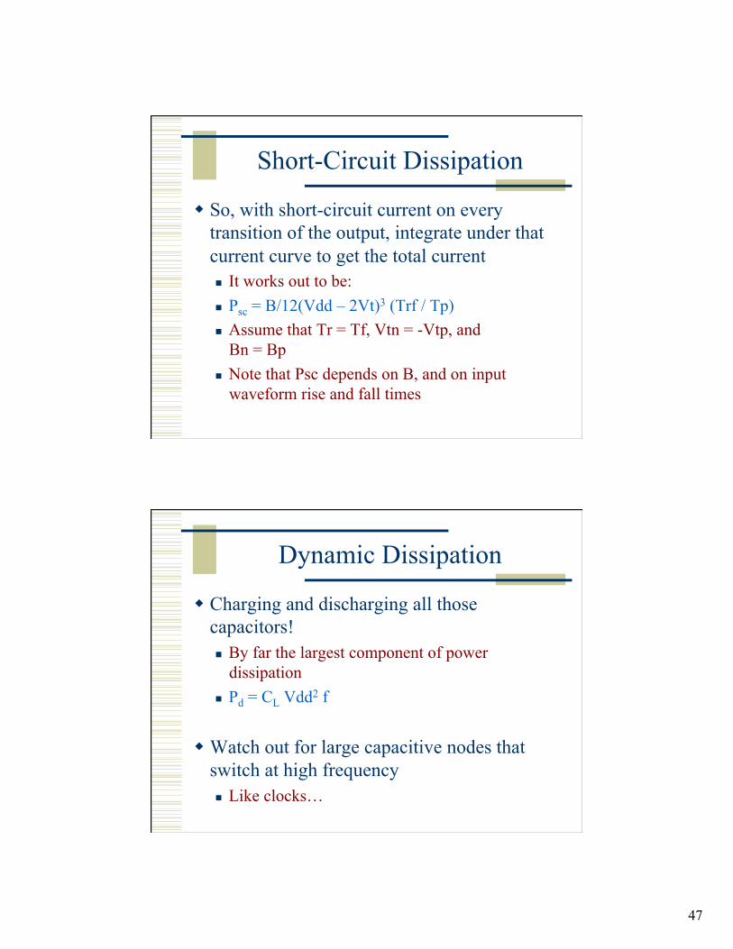
Static Leakage Power
That’s the leakage current For static power dissipation:
Ps = SUM of (I X Vdd) for all n devices For example, inverter at 5v leaks about
1-2 nW in a .5u technology Not much… …but, it gets MUCH worse as feature size
shrinks!
Short-Circuit Dissipation
When a static gate switches, both N and P devices are on for a short amount of time Thus, current flows during that switching time
47
Short-Circuit Dissipation
So, with short-circuit current on every transition of the output, integrate under that current curve to get the total current It works out to be: Psc = B/12(Vdd – 2Vt)3 (Trf / Tp) Assume that Tr = Tf, Vtn = -Vtp, and
Bn = Bp Note that Psc depends on B, and on input
waveform rise and fall times
Dynamic Dissipation
Charging and discharging all those capacitors! By far the largest component of power
dissipation Pd = CL Vdd2 f
Watch out for large capacitive nodes that switch at high frequency Like clocks…
48
Total Power
These are pretty rough estimates It’s hard to be more precise without CAD
tool support It all depends on frequency, average switching
activity, number of devices, etc. There are programs out there that can help
But, even a rough estimate can be a valuable design guide
Ptotal = Ps + Psc + Pd
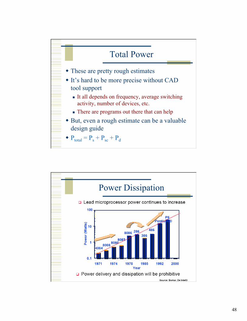
Power Dissipation
49
Heat Dissipation
60 W light bulb has surface area of 120 cm2
Core2 Duo die dissipates 75 W over 1.4 cm2
Chips have enormous power densities Cooling is a serious challenge
Graphics chips even worse NVIDIA GTX480 – 250 W in ~3 cm2
Package spreads heat to larger surface area Heat sinks may increase surface area further Fans increase airflow rate over surface area Liquid cooling used in extreme cases ($$$)
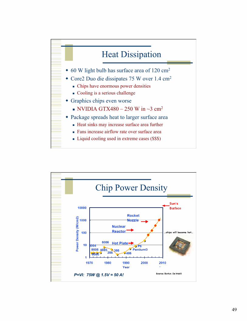
Chip Power Density
50
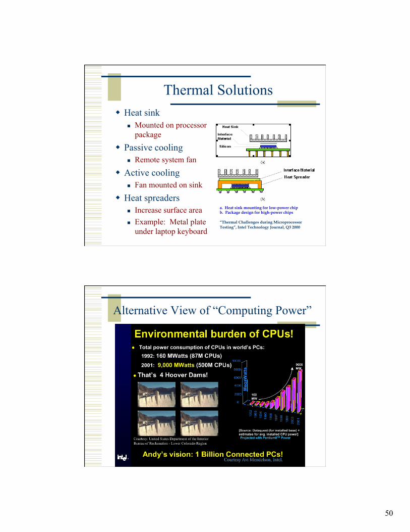
Thermal Solutions Heat sink
Mounted on processor package
Passive cooling Remote system fan
Active cooling Fan mounted on sink
Heat spreaders Increase surface area Example: Metal plate
under laptop keyboard
a. Heat sink mounting for low-power chip b. Package design for high-power chips
“Thermal Challenges during Microprocessor Testing”, Intel Technology Journal, Q3 2000
Alternative View of “Computing Power”
51
Power Management on Pentium 4
Over 400 power-saving features! 20% of features = 75% of saved power
Clock throttling Thermal diode temperature sensor Stop clock for a few microseconds Output pin can be used by system to trigger other
responses SpeedStep technology for mobile processors
Switch to lower frequency and voltage Depends on whether power source is battery or AC Can be manually overridden by Windows control panel
“Managing the Impact of Increasing Microprocessor Power Consumption”, Intel Technology Journal, Q1 2001
Pentium 4 Multi-level Powerdown
Level 0 = Normal operation (includes thermal throttle) Level 1 = Halt instructions (less processor activity) Level 2 = Stop Clock (internal clocks turn off) Level 3 = Deep sleep (remove chip input clock) Level 4 = Deeper sleep (lower Vdd by 66%)
For “extended periods of processor inactivity” QuickStart technology – resume normal operation from
Deeper Sleep Note: We haven’t even talked about system powerdown
modes, like removing power from processor, stopping hard disks, dimming or turning off the display…
“Managing the Impact of Increasing Microprocessor Power Consumption”, Intel Technology Journal, Q1 2001
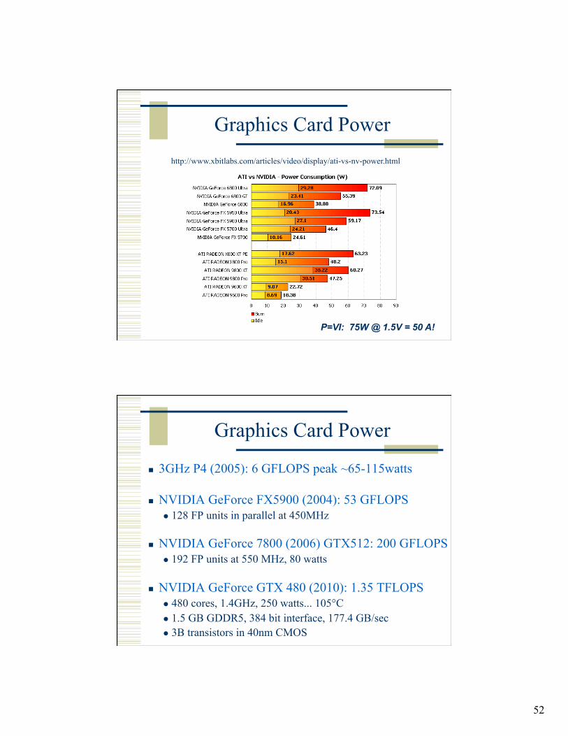
52
Graphics Card Power http://www.xbitlabs.com/articles/video/display/ati-vs-nv-power.html
Graphics Card Power
3GHz P4 (2005): 6 GFLOPS peak ~65-115watts
NVIDIA GeForce FX5900 (2004): 53 GFLOPS 128 FP units in parallel at 450MHz
NVIDIA GeForce 7800 (2006) GTX512: 200 GFLOPS 192 FP units at 550 MHz, 80 watts
NVIDIA GeForce GTX 480 (2010): 1.35 TFLOPS 480 cores, 1.4GHz, 250 watts... 105°C 1.5 GB GDDR5, 384 bit interface, 177.4 GB/sec 3B transistors in 40nm CMOS
Related Documents