Design and Implementation of an Optical Code Division Multiple Access System Combined with Dense Wavelength Division Multiplexing Von der Fakultät für Informatik, Elektrotechnik und Informationstechnik der Universität Stuttgart zur Erlangung der Würde eines Doktor - Ingenieurs (Dr.-Ing.) genehmigte Abhandlung vorgelegt von Yongjun Zhang aus Beijing, China Hauptberichter: Prof. Dr.-Ing. Joachim Speidel Mitberichter: Prof. Dr.-Ing. Manfred Berroth Tag der mündlichen Prüfung: 05. Dezember 2003 Institut für Nachrichtenübertragung der Universität Stuttgart 2003

Welcome message from author
This document is posted to help you gain knowledge. Please leave a comment to let me know what you think about it! Share it to your friends and learn new things together.
Transcript
Design and Implementation of an
Optical Code Division Multiple Access System
Combined with Dense Wavelength Division Multiplexing
Von der Fakultät für Informatik, Elektrotechnik und Informationstechnik
der Universität Stuttgart zur Erlangung der Würde
eines Doktor - Ingenieurs (Dr.-Ing.) genehmigte Abhandlung
vorgelegt von
Yongjun Zhang aus Beijing, China
Hauptberichter: Prof. Dr.-Ing. Joachim Speidel
Mitberichter: Prof. Dr.-Ing. Manfred Berroth
Tag der mündlichen Prüfung: 05. Dezember 2003
Institut für Nachrichtenübertragung der Universität Stuttgart
2003
1
Acknowledgements
The work presented in this thesis was carried out at the Institut für Nachrichtenübertragung,
University of Stuttgart under the supervision of Professor Joachim Speidel. I would like to
express my gratitude to him for providing a conducive environment for performing this
research at his institute. His advice and encouragement have been an invaluable guidance
throughout this project. I also would like to thank Professor Manfred Berroth for acting as a
co-examiner. I am also grateful to my colleagues at the institute. Their knowledge and
expertise have been very valuable to me and I like to thank them for sharing those with me. I
also want to thank Friedrich-Ebert foundation for their scholarship at the first two years of my
studies. Finally, I am very indebted to my wife for her full support during my studies in
Germany.
Stuttgart, June 2003
Yongjun Zhang
2
Contents
Acknowledgements ................................................................................................................... 1
Contents..................................................................................................................................... 2
Abstract..................................................................................................................................... 5
Zusammenfassung .................................................................................................................... 5
Notation..................................................................................................................................... 6
Abbreviations ............................................................................................................................ 8
Chapter 1 Introduction......................................................................................................... 10
Chapter 2 Fundamentals of OCDMA................................................................................. 13
2.1 Using OCDMA in Optical Access Network............................................................... 13
2.2 Classification of OCDMA .......................................................................................... 14
2.3 Model of DS-OCDMA System .................................................................................. 15 2.3.1 Transmitter:....................................................................................................... 16
2.3.2 Receiver ............................................................................................................ 17
2.4 Code of DS-OCDMA System .................................................................................... 19
2.5 Parameters of OCDMA .............................................................................................. 21
Chapter 3 Experimental Results for OCDMA................................................................... 24
3.1 Incoherent Direct Sequence OCDMA ........................................................................ 24
3.2 Coherent DS-OCDMA ............................................................................................... 25
3.3 Frequency Encoded OCDMA..................................................................................... 28
3.4 Fast Frequency Hopping (FFH) OCDMA.................................................................. 31
3.5 PSK-OCDMA............................................................................................................. 32
3.6 The Other Methods ..................................................................................................... 36
3.7 Some Methods for Improving the Performance of OCDMA..................................... 40
3.8 Conclusion.................................................................................................................. 42
Chapter 4 OCDMA with Combined Electrical and Optical En/Decoding ...................... 44
3
4.1 The System Model...................................................................................................... 44 4.1.1 The Impulse Shape of Chips ............................................................................. 45
4.1.2 Electronic Encoder ............................................................................................ 46
4.1.3 Optical Modulator............................................................................................. 47
4.1.4 Optical Encoder and Decoder ........................................................................... 50
4.1.5 Optical Channel (Optical Fiber)........................................................................ 52
4.1.6 O/E Converter with Electronic Amplifiers ....................................................... 53
4.1.7 Electronic Decoder............................................................................................ 53
4.2 Interferometric Noise .................................................................................................. 54 4.2.1 Characteristics of Interferometric Noise ........................................................... 54
4.2.2 The Source of the Phase Noise ......................................................................... 56
4.3 The Results of the Simulation..................................................................................... 57 4.3.1 The Noise in the Optical Encoder..................................................................... 57
4.3.2 The Noise Performance of Optical Decoder..................................................... 61
4.3.3 The Performance of Electronic Decoder........................................................... 63
4.3.4 The Effect of Width of Chip Impulse ............................................................... 64
4.3.5 Summary........................................................................................................... 65
4.4 The Channel Coding ................................................................................................... 65 4.4.1 Reed-Solomon Code ......................................................................................... 66
4.4.2 Convolutional Code .......................................................................................... 68
Chapter 5 Implementation of a Prototype .......................................................................... 69
5.1 Experimental System.................................................................................................. 69
5.2 Signal Source and Scrambler ...................................................................................... 72
5.3 Impulse Generator ...................................................................................................... 75
5.4 Encoder/Decoder ........................................................................................................ 78 5.4.1 The Codeword................................................................................................... 78
5.4.2 Electronic Encoder ............................................................................................ 80
5.4.3 Optical Encoder................................................................................................. 82
5.4.4 Electronic Decoder............................................................................................ 83
5.4.5 Optical Decoder ................................................................................................ 84
5.5 Optical Transmitter and Receive r ............................................................................... 85 5.5.1 Electronic/Optical Converter ............................................................................ 85
5.5.2 Optical Receiver................................................................................................ 90
4
5.6 Data Recovery ............................................................................................................ 91 5.6.1 Clock Recovery................................................................................................. 91
5.6.2 Phase Tracking.................................................................................................. 92
5.7 Channel Code.............................................................................................................. 95
5.8 Measurement Results .................................................................................................. 96
Chapter 6 OCDMA Combined with DWDM..................................................................... 98
6.1 The Fundamentals of WDM ....................................................................................... 98
6.2 The Feasibility of the CDMA/WDM System........................................................... 100
6.3 Network Architecture and Management................................................................... 103
Chapter 7 Conclusions ........................................................................................................ 105
Appendix ............................................................................................................................... 107
Appendix A1 An Algorithm of BER with Hard- limiter ................................................ 107
Appendix A2 Optical Splitter and Adder ...................................................................... 111
Appendix B Results of the Hardware Experiments ....................................................... 112
Bibliography ......................................................................................................................... 125
5
Abstract
To improve the flexibility and the capability of optical access networks, the investigations of this dissertation have been focused on applying optical code division multiple access (OCDMA) in the upstream of the access network. The noise caused by the interference between the same optical sources and different optical sources with the same and different wavelengths has been analyzed for the optical en/decoder. For a narrowband optical source, the interferometric noise produced by the variation of temperature of optical components restricts the signal processing within the optical domain. Therefore, a scheme with electronic en/decoding process has been proposed. An OCDMA demonstration system involving three users has been developed in the laboratory. The users can access the passive optical network in an asynchronous mode. The implementation of the OCDMA encoder and decoder has been done with both optical and electrical signal processing, respectively. The combination of OCDMA and dense wavelength multiplexing (DWDM) has been analyzed. To improve the performance of data and clock recovery, a new scheme of a phase tracing circuit has been designed. Some channel codes which could be suitable for OCDMA channels have been also investigated.
Zusammenfassung
Die vorliegende Dissertation befasst sich mit der Erhöhung der Flexibilität optischer Zugangsnetze durch den Einsatz der optischen Codevielfachzugriffstechnik (OCDMA, Optical Code Division Multiple Access). Dabei werden die Rückkanäle hoher Bitrate in einem passiven optischen Teilnehmeranschlussnetz (PON) betrachtet. Das Rauschen, das aus der Interferenz zwischen Lichtwellen gleicher oder unterschiedlicher Quellen entsteht, wird für optische Codierer und Decodierer analysiert. Für schmalbandige optische Quellen wird die Güte der nichtkohärenten optischen Signalverarbeitung durch dieses interferometrische Rauschen, das im wesentlichen durch Temperaturschwankungen in den optischen Komponenten entsteht, beschränkt. Deshalb wird auch ein Verfahren mit elektrischen OCDMA-Codiern und -Decodiern untersucht. Ein OCDMA-Demonstrationssystem mit drei Teilnehmern wird im Labor aufgebaut. Jeder Teilnehmer kann asynchron auf das passive optische Anschlussnetz zugreifen. Die Verfahren mit optischen als auch elektrischen Codierern und Decodierern werden theoretisch und experimentell untersucht. Ferner wird eine Kombination von optischem Code- und Wellenlängenmultiplex (DWDM) vorgestellt. Hierzu wird eine neue Schaltung für die Daten- und Taktrückgewinnung entworfen. Ferner werden geeignete Verfahren der Kanalcodierung vorgestellt, welche die Bitfehlerhäufigkeit bei einer größeren Zahl zugeschalteter Nutzer auf ein zulässiges Maß verringern können.
6
Notation
b – propagation constant
Β – input beam radius
hB – the power equivalent bandwidth of h(t)
rB – the bandwidth of electronic receiver
c – the speed of light in vacuum
lc – specifies a codeword
D – chromatic dispersion coefficient of optical fiber
DM – material dispersion
DW – waveguide dispersion
f(t) – impulse response of the equalized filter of the optical receiver and amplifiers
nfλ – the center frequency of the laser with the wavelength nλ
F(s) – the Laplace transform of f(t)
h(t) – impulse response of the CDMA decoder filter
I(t) – the output of the driver of Laserdiode
bI – the bias current of Laserdiode
thI – the threshold of Laserdiode
L – the distance of the transmission
CL – the length of the codeword
cl – the length of the delay line for one chip duration
N – the number of accessed users
gn – the group index in the core of the fiber
oN – power spectral density of the noise
CCP – bit error probability after convolutional decoding
chP – the loss of optical power in fiber
deP – the loss of optical power at the optical decoder
eP – bit error probability of OCDMA link
7
enP – the loss of optical power of the optical encoder
LDP – optical power emitted by the Laserdiode
mP – optical margin of a optical link
maxP – the maximum optical power
markP – the optical power of mark ( “1” )
NullP – the optical power of Null ( “0” )
PONP – the loss of optical power at PON
rP – probability
RSP – bit error probability after RS decoding
SP – symbol error probability
thP – the approximate value of optical power with threshold current
R – reflectivity of the interferometer mirror
ℜ – redundancy of the channel code
chipR – the ratio between number of “1” chips and total number of chips within a codeword
DR – bit rate of user data
maxR – the maximum data rate of transmission through an OCDMA channel
CT – the duration of a chip
DT – the duration of the user bit
∆TD – the impulse degradation from dispersion
Tg – group delay in fiber
w – code weight
η – the efficiency of optical electronic conversion
λ – the wavelength of the light in vacuum
λ∆ – the linewidth of optical source
aλ – auto-correlation
cλ – cross-correlation
θ – the threshold of the decision
ω – the angular frequency of the light
cτ – the coherence-time of the optical source
∗ – denotes a convolution
8
Abbreviations
ASE – amplified spontaneous emission
ATM – asynchronous transfer mode
ATC – automatic temperature control
BER – bit error ratio
CC – convolutional code
CDMA – code division multiple access
CW – continuous wave
DC – dispersion compensation
DD – direct detection
DFB Laser – distributed feedback Laser
DS-CDMA – direct sequence CDMA
DWDM – dense WDM
EAM – electro-absorption modulator
ECL – emitter-coupled logic
EDFA – erbium doped fiber amplifier
EXT – extinction ratio of the optical transmitter
FDMA – frequency division multiple access
FEC – forward error correction
FIR – finite impulse response
FTTH – fiber to the home
FWHM – full-width half-maximum
FWM – four-wave mixing
GVD – group velocity dispersion
HFC – hybrid fiber-coax
IMD – inter-modulation distortion
IM-DD – intensity modulation direct-detection
IMP – inter-modulation product
ISI – intersymbol interference
ITU – International Telecommunications Union
9
LED – light emitting diode
MAI – multi-access interference
MFD – matched-filtered detection
OCDMA – optical CDMA
ONU – optical network unit
OLT – optical line terminal
OTDMA – optical time division multiple access
PLC – planer lightwave circuit
PMD – polarisation mode dispersion
PON – passive optical network
PRBS – pseudo random bit sequence
PSK – phase shift keying
RF – radio frequency
SBS – stimulated Brillouin scattering
SCM – subcarrier multiplexing
SDH – synchronous digital hierarchy
SPM – self-phase modulation
SRS – stimulated Raman scattering
SSFBG – superstructured fiber Bragg gratings
SSMF – standard single-mode fiber
TEC – thermoelectric cooler
TDMA – Time Division Multiple Access
TR – thermistor resistance
WDM – Wavelength Division Multiplexing
XPM – cross-phase modulation
10
Chapter 1 Introduction
For backbone networks, in recent years there has been a rapid increase in the capability of
transmitting high rate data with the usage of both time division multiplexing (TDM) and
wavelength division multiplexing (WDM) technologies within the optical domain. Also
optical fibers will inevitably become the transmission medium of metropolitan area networks
(MANs). While the capacity of the rest of the network has been increased, the access network
constructed with twisted wires and coaxial cables has become the bottleneck in providing
larger bandwidth to users. The expansion of the usage of the Internet has already caused an
increase in the demand for bandwidth in the access networks. Although current broadband
access technologies such as digital subscriber lines (DSL) and cable modems are sufficient for
some applications such as Web surfing and email, one can foresee an increasing demand for
bandwidth outstripping the nowadays supply. The Internet enables bandwidth-intensive
applications such as streaming media, video on demand and video telephony applications. In
turn, these applications drive up the demand for larger bandwidth [1, 2]. As far as
transmission capacity is concerned, optical fiber has no competition, and now it is
increasingly extending to access networks. Access networks face more challenges than other
pure transmission networks. Protocols, multi-service capability and cost are the dominant
issues. Optics has a number of advantages concerning the above issues of networking if a
suitable transmission approach is used in the optical networks. Optical code division multiple
access (OCDMA) is one suitable technology for this aim [3, 4].
Code division multiple access (CDMA) technology was developed for wireless military
telecommunications at the end of the 1970 in order to increase the robustness security of the
information transmission [3]. It is also called spread spectrum technique, and has been used
for a long time in military communications to resist intentional jamming and to achieve low
probability of detection. Now CDMA is one of the most useful technologies in the wireless
area, especially for the third generation wireless system [3, 5]. OCDMA scheme is a kind of
CDMA scheme in which code multiplexing and transmission are performed in the optical
domain.
11
OCDMA supports multiple concurrent accesses to the same time slots and the same frequency
range. It is seen as another kind of multiplexing technique besides TDMA and WDM, and it is
a potential candidate for the future optical network, especially for the access network due to
easy access and flexible network architectures [4, 7, 10, 11]. Compared to TDMA, OCDMA
has the advantages to be compatible with the bursty and asynchronous network traffic,
especially in upstream links. The asynchronous multiplexing by OCDMA systems is a very
desirable feature compared to any other digital multiplexing techniques at high data rates.
Optical time division multiple access (OTDMA) has the inherent problem of accreting phase
of each sub-signal whereas with OCDMA transmission capacity is sacrificed. OCDMA has
been considered as a desirable choice for local area networks which are usually implemented
in passive optical network (PON) topology. In the mid 80’s, researches began to focused on
the selection of codewords and network architectures, and since then OCDMA has become a
branch of optical communications.
It is generally believed that the OCDMA enables fast processing of signals in the optical
domain which could help to reduce the complexity of the electronics hardware and software
existing in current communications networks, and could also allow more flexible networks
[7]. However, though CDMA is successful as a communication technology in the radio,
microwave and millimeter wave bands [12], a commercial optical communication system
using OCDMA technology has not yet been realized and research is still in laboratory status.
The few available complete OCDMA demonstration systems actually have not yet
demonstrated the expected advantages of OCDMA. A number of components still needs to be
developed, such as optical sources, en/decoder and broadband optical amplifiers etc. [2, 4].
In this thesis, a new approach is developed by using an electronic en/decoding process in
OCDMA for optical access networks. Based on the study of the results of the current
experimental research and the analysis of the optical beat interference noise, a prototype with
the chiprate of up to 3Gchips/s has been implemented. It offers 3 OCDMA channels for a
variety of data sources with total throughput of 450Mbit/s. The scheme is oriented for
practical usage in the upstream channels of PON access networks. This system has the
following advantages:
a) use of electronic encoder and decoder to avoid the optical interferometric noise produced
by optical encoder and decoder,
b) the bit error rate is reduced by using an electronic logic decoder which has the function of a
hard-limiter,
12
c) easy to be integrated into DWDM system with narrowband optical sources.
This thesis is organized as follows:
Chapter 2 introduces the basic concepts of access networks, the mathematical model of the
traditional OCDMA scheme, and the comparison of OCDMA with wireless CDMA.
Chapter 3 presents a survey of recent experimental results in the area of OCDMA. It was
found that none of existed OCDMA demonstration system is suitable for practical usage and
the OCDMA technology is currently not mature.
In Chapter 4 the noise characteristics of OCDMA are analyzed. The simulation of optical
carrier is carried out taking into account the coherent noise source caused by temperature
wandering. The limitation of OCDMA is then evaluated.
Chapter 5 describes the implementation of an OCDMA system with both optical and
electrical en/decoders for comparison. An experimental 3-channel OCDMA demonstration
system is developed with a capacity of 150Mbit/s at BER 10 and 100Mbit/s at BER 10
for each channel. With simple error correction coding, BER can be improved much beyond
.
6− 12−
1210−
In Chapter 6 the feasibility and the performance of OCDMA combined with DWDM system
are analyzed.
Finally, conclusions are drawn in Chapter 7.
13
Chapter 2 Fundamentals of OCDMA
Traditional ways of separating signals in time (i.e. TDMA) or in frequency (i.e. FDMA) are
simple to make sure that the signals are orthogonal and non-interfering. However, in CDMA,
different users occupy the same bandwidth at the same time, but they are separated from each
other by the use of a set of orthogonal waveforms, sequences, or codes. The purpose of this
chapter is to provide the fundamentals of optical code-division multiple access technology.
2.1 Using OCDMA in Optical Access Network
The access network provides transport bearer capabilities for the provision of
telecommunications services between a service node interface to a service node and each of
the associated interfaces towards the customer premises networks [8]. With the highly
employed technology in the long haul backbone network and MAN, it becomes more and
more important to employ suitable technology in the access network in order to access more
users and offer high bit rate link to end users. Passive optical network (PON), in which
passive optical components are located between a hub and an optical network unit (ONU), is a
recommended architecture for optical access network nowadays [2]. Bus/tree topologies are
envisages in this architecture due to their expected lower maintenance costs [13]. Before the
achievement of the fiber to the home (FTTH) solution, the access network is typically built as
hybrid fiber-coax (HFC) network [1]. In a PON the fiber outgoing from the optical line
terminal (OLN) in the service node is split by a passive optical splitter, where all ONUs are
connected with separate fibers. In this way, the bandwidth and facilities can be shared by all
ONUs to reduce the access costs. In this case, the use of OCDMA in the upstream (from
ONUs to OLT) is superior to the now widely used TDMA system, in the sense that OCDMA
can simultaneously offer many asynchronous channels [15]. If CDMA is combined with
DWDM, the access number would be further increased.
14
PassiveOptical
Network(PON)
Data Source
#1
Data Source
#N
CDMAEncoder
CDMAEncoder
CDMADecoder
CDMADecoder
DataRecovery
#N
DataRecovery
#1Optical
Figure 2.1 A block diagram of an OCDMA system used in PON
Figure 2.1 shows a block diagram of an OCDMA system used in PON. A typical transmitter
for OCDMA is composed of a date source and an encoder. If the data source is electrical, the
electrical CDMA encoder is followed by a laser to provide an optical signal. In case the data
sequence is optical, the CDMA encoder is an optical device implemented with optical signal
processing. The CDMA encoder maps each output bit of the data source into a high rate
sequence of chip impulses. Thus, on the fiber we have an OCDMA signal. At the receiver the
optical impulse sequence is processed for data recovery. There are N transmitter and receiver
pairs (users). Each transmitter has a different CDMA code word, also called signature or
signature sequences. Thus, a common optical fiber can be shared by N users using their own
optical sequence.
2.2 Classification of OCDMA
In OCDMA schemes there is no simple rule of thumb to relate process gain and signal
bandwidth. Any combination of spatial, temporal, frequency and polarization information can,
in principle, be used for OCDMA coding [11]. There are several different approaches to
design encoders for optical schemes. Two commonly used methods will be discussed here.
Spreading: This is a common method to implement OCDMA. At the transmitter, a short
optical impulse, with chip duration T , which is much smaller than the data bit duration T ,
is fed into an FIR filter composed of optical delay lines. The output is a high-rate impulse
train that constitutes the transmitter code sequence. At the receiver, a similar filtering
C D
15
operation is performed on the intensity (incoherent) of the incident signals by an optical delay
line filter acting as a decoder. Only a signal that is matched to the decoder is despread in time,
with a concomitant increase in peak level compared to unmatched signals. The decoder output
signal can be discriminated by a threshold device. This method is also called direct sequence
OCDMA (DS-OCDMA) or on-off keying (OOK) OCDMA. In order to enhance effectivity of
the decoder, coherent matched filtering can be used for restructuring the original impulse. The
principle advantage of the coherent approach is that for an encoder that produces w chip
impulses, the coherently decoded signal has an intensity w times greater than an incoherent
superposition. For coherent decoder, this intensity is a fixed fraction of the total energy
entering the decoder which is independent of w.
Spectral coding: It uses broadband continuous wave (CW) sources and performs
coding directly in the optical frequency domain. In this approach the spectrum is divided into
W slices and encoded by a W-element users codeword. The mapping of the physical mask
pattern (e.g. using a liquid crystal array) to an optical spectral code allows a wide range of
codes to be employed. This approach is also called frequency encoded OCDMA.
The various fundamental approaches can be combined among themselves or combined with
other modulation schemes to form new solutions. For example, fast frequency hopping (FFH)
is a combination of spreading in time and spectral coding [32], and PSK-en/decoding
OCDMA results from the combination of time spreading and PSK scheme [40]. The
commonly called OCDMA system mostly refers to incoherent DS-CDMA.
2.3 Model of DS-OCDMA System
To simplify a concept of a traditional incoherent DS-OCDMA scheme, three assumptions are
made in the following mathematical model:
• Only a IM-DD optical system will be considered, i.e. optical converters use the optical
intensity modulation and direct intensity detection;
• The chip in the codeword (signature sequence) is represented by a rectangular
impulse;
• The optical sources are incoherent light sources.
16
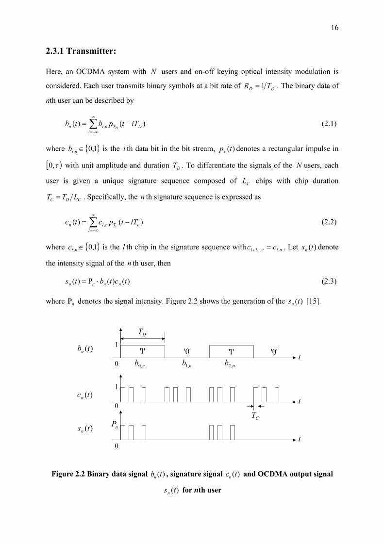
2.3.1 Transmitter:
Here, an OCDMA system with users and on-off keying optical intensity modulation is
considered. Each user transmits binary symbols at a bit rate of
N
DD TR 1= . The binary data of
nth user can be described by
∑∞
−∞=
−=i
DTnin iTtpbtbD
)()( , (2.1)
where is the i th data bit in the bit stream, denotes a rectangular impulse in 1,0, ∈nib )(tpτ
[ )τ,0 with unit amplitude and duration T . To differentiate the signals of the users, each
user is given a unique signature sequence composed of chips with chip duration
D N
CL
CD LC TT = . Specifically, the n th signature sequence is expressed as
∑∞
−∞=
−=l
cTnln lTtpctcc
)()( , (2.2)
where is the th chip in the signature sequence with c 1,0, ∈nlc l nlnLl cc ,, =+ . Let denote
the intensity signal of the th user, then
)(tsn
n
)()()( tctbts nnnn ⋅Ρ= (2.3)
where Ρ denotes the signal intensity. Figure 2.2 shows the generation of the [15]. n )(tsn
DT
'1' '1''0' '0' t
t
tnP
nb ,0 nb ,1 nb ,2
)(tcn
)(tbn
)(tsn
1
1
0
0
0
CT
Figure 2.2 Binary data signal , signature signal and OCDMA output signal
for nth user
)(tbn
s
)(tcn
)(tn
17
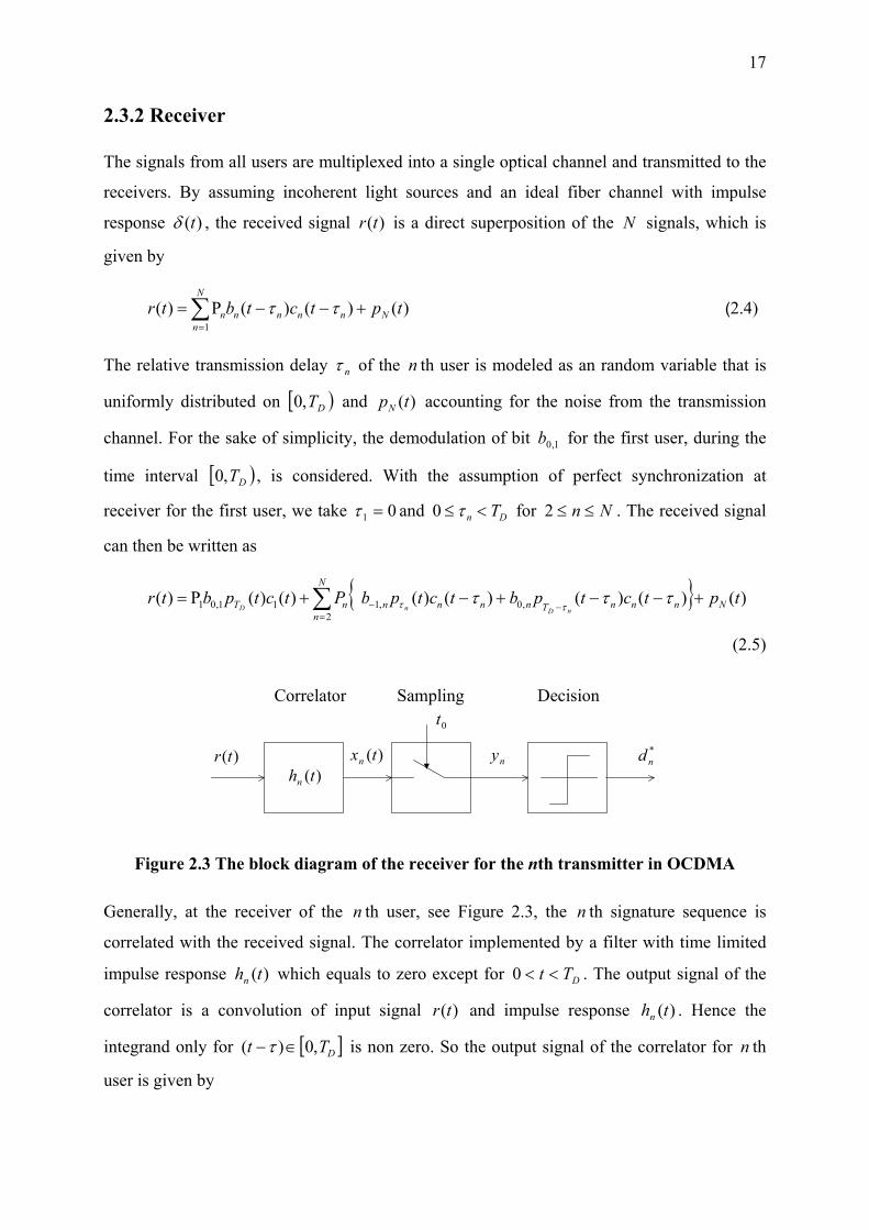
2.3.2 Receiver
The signals from all users are multiplexed into a single optical channel and transmitted to the
receivers. By assuming incoherent light sources and an ideal fiber channel with impulse
response )(tδ , the received signal is a direct superposition of the signals, which is
given by
)(tr N
)()()()(1
tptctbtrN
nNnnnnn∑
=
+−−Ρ= ττ (2.4)
The relative transmission delay nτ of the th user is modeled as an random variable that is
uniformly distributed on [ and accounting for the noise from the transmission
channel. For the sake of simplicity, the demodulation of bit b for the first user, during the
time interval [ , is considered. With the assumption of perfect synchronization at
receiver for the first user, we take
n
)t)DT,0 (pN
0
1,0
)DT,0
1 =τ and Dn T<≤ τ0 for Nn ≤≤2 . The received signal
can then be written as
∑=
−− +−−+−+Ρ=N
nNnnnTnnnnnT tptctpbtctpbPtctpbtr
nDnD2
,0,111,01 )()()()()()()()( τττττ
(2.5)
)(txn ny *nd
)(thn
0t
)(tr
Correlator Sampling Decision
Figure 2.3 The block diagram of the receiver for the nth transmitter in OCDMA
Generally, at the receiver of the th user, see Figure 2.3, the n th signature sequence is
correlated with the received signal. The correlator implemented by a filter with time limited
impulse response which equals to zero except for
n
)(thn DTt <<0 . The output signal of the
correlator is a convolution of input signal and impulse response . Hence the
integrand only for
)(tr )(thn
[ DT,0) ∈ ]t( −τ is non zero. So the output signal of the correlator for n th
user is given by
18
∫−
−⋅=∗=t
Ttnnn
D
dthrthtrtx τττ )()()()()( (2.6)
Because of the time limited impulse response of the correlator, only depends on the
received signal in time interval
)(txn
)(tr [ ]tTt D ,− . will be sampled at time instant t and
decided by the threshold device. The sampling occurs at the end of each bit, and the sampled
value at the time point t is
)(txn 0
DT=0
∫
∫
−⋅=
−⋅==−
D
D
T
Dn
t
Ttnnn
dttThtr
dttthtrtxty
0
000
)()(
)()()()(0
0 (2.7)
Now we only pay attention to the first user, and insert (2.5) into (2.7) and get for : 1=n
[ ] )()()()()( '
2,0,1011,001 tpbbPtbPty N
N
nnnnnnnnn +++= ∑
=
+−−
+ τρτρρ (2.8)
where denotes the noise of the decoder output, and are the cross-
correlations between the first user and th user which can be represented by
'Np )(τρ −
n )(τρ +n
n
.)()()()(
)()()()(
1
01
dttThtctp
dttThTtctp
D
T
nn
DDnTn
D
D
−−=
−+−=
∫
∫
+
−−
ττρ
ττρ
ττ
τ
τ
(2.9)
In the Eq.(2.8), the first term is the useful information of the sent signal, the second term is
the interference from the other sent signals (multi access interference, MAI) and the third term
is the result of correlation process of the noise from the transmission channel and other
sources.
The output of the decision device is
<≥
=θθ
)(,0)(,1
)(0
00
*
tyty
tdn
nn (2.10)
where θ is the threshold of the decision, its value depends on the codeword and other
parameters of the system and will be discussed later.
19
Because the correlation filter in the receiver is a matched filter for the corresponding
codeword , the impulse response of the filter can be expressed by the time inverse of
codeword, from Equation (2.2):
)(tcn
)()(1
0,
'cT
L
lnln lTtpctc
C
C
−⋅= ∑−
=
(2.11)
one can obtain:
))1(()(1
, cT
L
lnlLn Tltpcth
C
C
C−−⋅= ∑
=− (2.12)
For the traditional OCDMA-system only unipolar codewords are used which will be
discussed in the following .
2.4 Code of DS-OCDMA System
The choice of the codewords, the signature sequence, is a key problem to any successful
CDMA scheme, either electrical or optical. For an OCDMA system, in which multiple users
access the same medium using the same time interval and frequency band, the transmitted
concurrent data streams will inevitably produce multi access interference (MAI). In order to
reduce the effects of this interference, the code should meet specific conditions for auto- and
cross-correlation. The proper selection of codewords is more important for incoherent system
than for coherent system, because incoherent system has a higher MAI power level.
The bipolar codewords used in wireless communication play a little roll in non-coherent
OCDMA. This is because the optical signal is equivalent to the instant power which is
nonnegative. This means, that codes based on +1/−1 signals, which are used in wireless
CDMA system, cannot be applied in optical system. Thus for OCDMA, a new code criterion
needs to be designed. A good optical CDMA code has much more 0’s than 1’s in each
codeword, while a well-correlated (+1/−1) sequence typically has about the same number of
+1’s and –1’s. Up to now various code families for OCDMA have been suggested, from one-
dimensional (1-D) codes encoded in time-domain to the two-dimensional (2-D) codes
encoded both in time and wavelength [21] or time and space [30] domain. The code families
include Gold codes [20], symmetric quasi-prime codes [19], quadratic congruence code [17,
18], block-multiplex-code [21] and optical orthogonal code (OOC) [16]. The use of OOCs
enables a large number of asynchronous users to transmit information. Thus the lack of the
20
stringent requirement of network synchronization enhances the flexibility of the system. Now
the OOC is an important candidate for OCDMA used in access networks.
Optical Orthogonal Code: An optical orthogonal code (OOC) is a family of (0,1)
sequences with relatively good properties of auto- and cross-correlation. The auto-correlation
of each OOC codeword exhibits the “thumbtack” shape and the cross-correlation between any
two OOC codewords remains low at all time. The thumbtack shape of the auto-correlation
facilitates the detection of the desired signal, and the low cross-correlation reduces MAI in the
network. Here we give the definition and some fundamental properties of OOC. An optical
orthogonal code ),,,( caC wL λλ is a family of (0,1) sequences with length and weight w ,
which satisfies the following two properties [16]:
CL
1) The auto-correlation property:
∑−
=+ ≤
1
0
CL
tatt xx λτ (2.13)
for any and any integer 1,0∈tx τ , CL<< τ0 .
2) The cross-correlation property:
∑−
=+ ≤
1
0
CL
tctt yx λτ (2.14)
for any and any integer 1,0∈≠ tt yx τ .
In general, for , i.e. for a given integer code length and weight w, where
, and
)1,1,,( wLC
1 =a
CL
)1( −≤− CLww 1=cλλ , one can construct at most N codewords of OOC, the value
of N is upper bounded by
1,)1(
1≠
−−
≤ www
LN C (2.15)
where the symbol [ denotes the integer portion of the real value x. In the following, we only
consider codes with .
]x
( )1,1,, wLC
The Bit Error Ratio of OOC: The BER of OOC can be exactly calculated if we
assume that the chips are synchronous in the system between the users (for asynchronous
chips see [22]). At the receiver, we have multiple overlap. The output of the decision device is
given by Eq. (2.10). If the number of the impulses is equal to or higher than threshold θ , the
decision device outputs a “1” (Mark), otherwise a “0” (Null). If we assume that no random
noise is present in the system, then the false detection of a Mark as a Null is not possible
21
because, when a Mark is transmitted, the threshold is then definitely exceeded (θ must be
smaller than code weight w) and therefore a Mark is detected. But if the information bit is a
Null, it may be mistaken and detected as a Mark when MAI is present in the system.
Let us consider the detection of an individual user n. An impulse from another user sensed by
detector n is called a hit. When user n is sending Null, a false detection occurs when there are
θ or more hits. The cross-correlation property ( 1=cλ ) ensures that each fortuitous user
contributes at most with one hit. The probability of a hit from another user equals to CLw2
[22]. The bit error probability is given by [16]
ji
C
j
C
i
j
N
i
N
r
N
ire
Lw
Lw
ji
iN
sendingareusersotherietcectiondfalsePsendingareusersotheriPP
−
=
−
=
−
−
=
−
⋅
−=
⋅=
∑∑
∑221
1
11
2
1|121
θθ
θ
(2.16)
Algebraic manipulation gives the following alternative formula:
∑−
=
−−
−
−=
1 122
21
21
21 N
i
iN
C
i
Ce L
wL
wi
NP
θ
(2.17)
Obviously, when ( and wN <− )1 w=θ , 0=eP . The BER can be reduced by using the hard-
limiter before the decoder, this will be discussed in detail in Chapter 4 and Appendix A1.
The drawback, however, is that the number of different codewords, i.e., the number of users
in the system, is limited. The number of users that can be accommodated in an OOC system is
upper bounded by Eq. (2.15), given that the upper bound of to support required data rate.
This puts an upper bound on the number of impulses w that can be used for a given number of
users. So there is a tradeoff between the number of users and BER in system design.
CL
2.5 Parameters of OCDMA
A comparison between wireless CDMA and OCDMA is given in the Table 2.1. The main
difference lies in frequency of the carrier, i.e. the frequency of lightwave in OCDMA is much
higher than that of RF in wireless CDMA, and the phase of lightwave can not be well
controlled, and furthermore there is no ±1 for OCDMA. Though bandwidth in the optical
domain is much wider than that in wireless telecommunication, the spectral efficiency
22
remains nevertheless one of a number of important measures of system performance for high
speed network.
Table 2.1 Comparison of OCDMA with wireless CDMA
OCDMA Wireless CDMA
Carrier Lightwave
Phase can not be well controlled
Micro- and millimeter wave Limited availability
Spreading/despreading Time/Wavelength domain Time/Frequency domain
Direct sequence SS, Wavelength hopping
Direct sequence SS Frequency hopping
Code
Fewer Mark in codeword Balanced Mark and NullEn/decoding Optical domain RF domain or baseband Capacity Soft (on demand). Interference limited
Transmission medium Closed-space (optical fiber) Dispersive Low attenuation Nonlinear
Free-space (air) Multipath Large attenuation Linear
Interference suppression Open question Multisectored antenna Multibeam reception Synchronization Power control
Problems in propagation Dispersion effect Nonlinear effect Interferometric effect
Near-far effect Multipath effect Fading
In principle, OCDMA has many advantages like its counterpart in wireless. Compared with
TDM and WDM scheme, OCDMA also has the following advantages:
• Using optical processing to fulfill certain network applications such as addressing and
routing;
• Low delay access suitable to bursty local-area network traffic, effective allocation of
bandwidth responding to requirement, variable bit rate;
• High capability of data throughput and accessed users;
• Flexibility of the network architecture;
• High speed coding and decoding process;
• Asynchronous data transmission simplifies network planning, management and
control;
23
• High security of data and network.
The advantages of asynchronous transmission and the capability of multiple-access in a bursty
environment make OCDMA attractive for LAN applications. Hitherto, the capabilities of
OCDMA are not completely demonstrated, because science and technology are not yet fully
developed. The purpose of this thesis is to make a significant contribution.
24
Chapter 3 Experimental Results for OCDMA
There are many theoretical investigations on OCDMA, such as the selection of the
codewords, the study of various OCDMA structures and networks etc., but only a few
experimental studies can be found. The experimental research in the area of OCDMA began
in the mid 80’s with incoherent DS-CDMA system utilizing incoherent superposition of
optical intensity. In the mid 90’s, focus was on the coherent DS-CDMA which requires that
the optical delay has to be controlled within the scale of the optical wavelength in order to
achieve the correct phases of superimposed fields, and on frequency encoders (FE) which
operate in wavelength domain. With the development of the material and mechanical
technique, some new OCDMA schemes emerged, such as fast frequency hopping (FFH),
phase shift keying (PSK) OCDMA, etc.. Meanwhile non-digital OCDMA schemes have also
been proposed and have been experimentally investigated, and the results show that the non-
digital scheme is even better than others. There are many parameters to describe the
performance of an OCDMA system, such as bandwidth utility, chip period, bit rate and
number of users, etc.. In this chapter we briefly describe the current developments of
OCDMA technology through the experimental results in this area.
3.1 Incoherent Direct Sequence OCDMA
For incoherent DS-OCDMA, the optical processing at the receiver operates with the optical
intensity. According to the structure of the optical encoder/decoder, the early implementation
of OCDMA systems can be divided into two types, i.e. tapped delay lines and ladder networks
(the latter only for same special codewords).
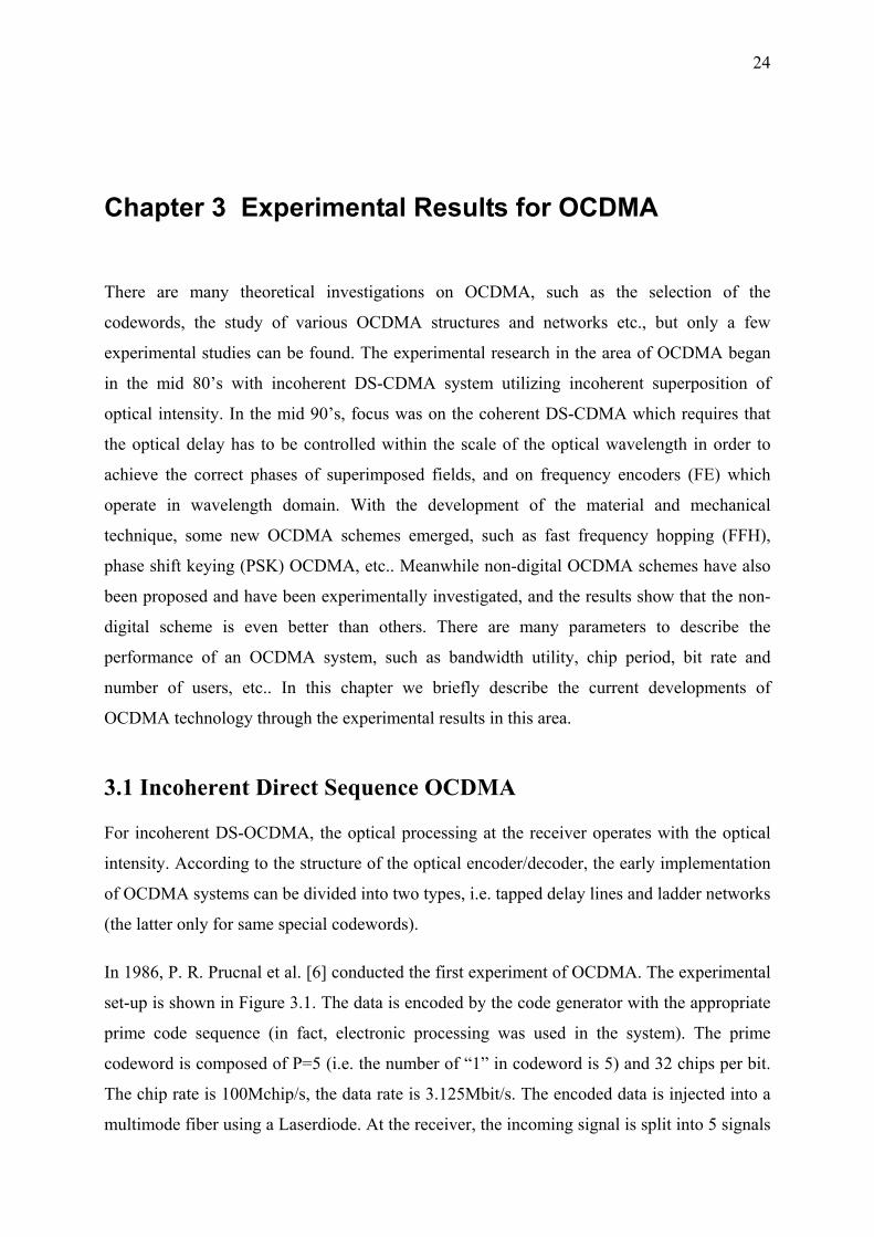
In 1986, P. R. Prucnal et al. [6] conducted the first experiment of OCDMA. The experimental
set-up is shown in Figure 3.1. The data is encoded by the code generator with the appropriate
prime code sequence (in fact, electronic processing was used in the system). The prime
codeword is composed of P=5 (i.e. the number of “1” in codeword is 5) and 32 chips per bit.
The chip rate is 100Mchip/s, the data rate is 3.125Mbit/s. The encoded data is injected into a
multimode fiber using a Laserdiode. At the receiver, the incoming signal is split into 5 signals
25
at first. Then the optical correlator selectively delays the signals before recombining them.
This processed signal impinges on an avalanche photodiode. In 1987, Salehi et al. also
demonstrated a two-transmitter OCDMA-system with optical tapped delay lines decoder [48].
Holmes and Syms implemented an optical processing using ladder networks and measured the
auto-correlation and cross-correlation [19]. At the Institute of Telecommunication, University
of Stuttgart, a demonstration system with electronic encoder and optical decoder has been
implemented. It has four users with a chip rate of 720Mchip/s [15].
D ata G enerator
&B ER Tester
C odeG enerator
LaserDriver
PulseG enerator
ThresholdD etector
A PD andPreA m p
C om biner
O ptical D elay Line
SplitterStar
C oupler
R eceived D ata
Transm itted D ata
C oded D ata
O ptical Signal
Receiver
Figure 3.1 The first experiment for the OCDMA system (see Figure 7 in [6])
Most of the incoherent DS-OCDMA systems were used to demonstrate the feasibility of the
conception of OCDMA. In these early systems, broadband optical sources were used, and in
some cases, multimode fibers were used. To avoid large optical loss with optical processing,
the electronic processing was used only either at encoder or at decoder.
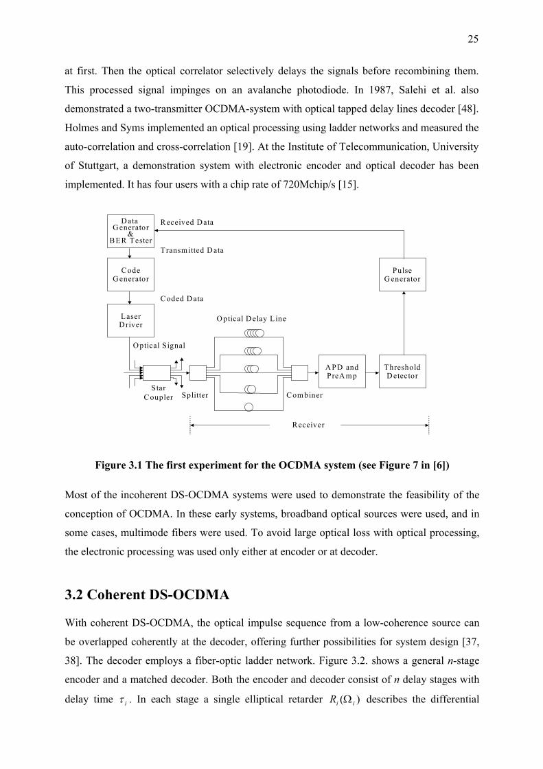
3.2 Coherent DS-OCDMA
With coherent DS-OCDMA, the optical impulse sequence from a low-coherence source can
be overlapped coherently at the decoder, offering further possibilities for system design [37,
38]. The decoder employs a fiber-optic ladder network. Figure 3.2. shows a general n-stage
encoder and a matched decoder. Both the encoder and decoder consist of n delay stages with
delay time iτ . In each stage a single elliptical retarder )( iiR Ω describes the differential
26
birefringence between the two arms. With delays chosen such that ∑ −
=> 1
1
n
i in ττ , an n-stage
encoder transforms an input impulse into a sequence of n2 impulses with equal intensity.
Each impulse represents a chip of the codeword. When the impulse sequence is decoded by an
identical network, impulses which have traversed alternative paths through the system with
the same total delay will be superimposed. Coherent summation can be achieved if delay time
i'τ of each decoder is matched to the corresponding encoder delay iτ such that cii τττ <− ' ,
where cτ is the coherence-time of the source. It is also necessary to ensure that all output
impulses have the same state of polarization, which can be achieved by controlli ng the
birefringence of one arm of each delay stage. Consider birefringence in the delay networks as
shown in Fig 3.2, where the differential retardation of stage i is denoted by an operator iR of
rotation magnitude iΩ on the Poincare sphere.
)( 1Ω1R
1τ
)( 22 ΩR
2τ
)( nnR Ω
nτ
)'(' 1Ω1R
1'τ
)'(' 22 ΩR
2'τ
)'(' nnR Ω
n'τ
LD
PD
Fiber downlead
Encoder
Matched Decoder
pulsesn2
Figure 3.2 The DS-OCDMA system with optical ladder networks (see Figure 1 in [37])
Without external control, the optical phase difference between interfering terms is random and
slowly drifts as optical path lengths fluctuate with ambient temperature changes. Hence
decoder must include the equipment for phase adjustment, although optical phase of
lightwave is diff icult to follow with the disturbance of temperature. Only two approaches
were proposed to solve this problem.
27
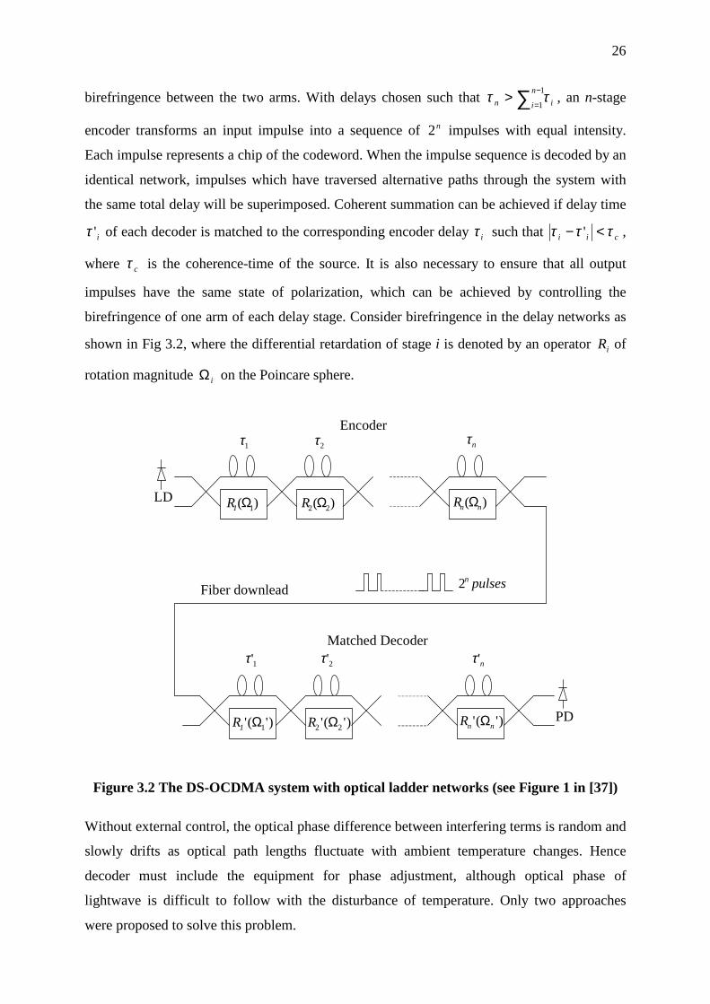
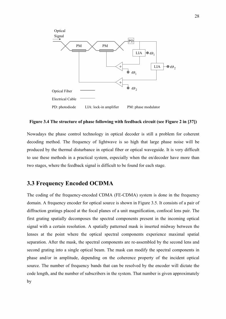
In [38] a mechanic equipment is introduced, that can statically adjust the optical phase. A
specially designed fiber stretching device with fine adjustment is used by winding part of one
of the 22m delay lines on two sets of pulley fixtures, pulling one of the one-axis movable
fixture by means of a micrometer head and a long arm lever while the other fixture is fixed in
the experiment (see Figure 3.3). In [37] an active phase controller is demonstrated. Thermal
phase modulators consisting of several 10cm of metal-coated fiber were used to provide the
phase control. These devices utilize temperature-induced refractive index changes in the fiber
core to achieve large phase excursions. The feedback circuit for servo-control of the
differential optical phase is shown in Figure 3.4. Here only two stages in decoder are
demonstrated. Only the outputs of the decoder were given in these two reports without giving
the results of BER of data transmission for the systems.
pivot
Lever
Pulley Fixture
MicrometerHead
Optical Fiber
Figure 3.3 The structure of the mechanic phase adjusting equipment (see Fig. 11 in [38])
28
OpticalSignal
PM PMPD
LIA
+
+
LIA
1ω
1ω
2ω
2ω
Optical Fiber
Electrical Cable
PD: photodiode LIA: lock-in amplifier PM: phase modulator
Figure 3.4 The structure of phase following with feedback circuit (see Figure 2 in [37])
Nowadays the phase control technology in optical decoder is still a problem for coherent
decoding method. The frequency of lightwave is so high that large phase noise will be
produced by the thermal disturbance in optical fiber or optical waveguide. It is very difficult
to use these methods in a practical system, especially when the en/decoder have more than
two stages, where the feedback signal is difficult to be found for each stage.
3.3 Frequency Encoded OCDMA
The coding of the frequency-encoded CDMA (FE-CDMA) system is done in the frequency
domain. A frequency encoder for optical source is shown in Figure 3.5. It consists of a pair of
diffraction gratings placed at the focal planes of a unit magnification, confocal lens pair. The
first grating spatially decomposes the spectral components present in the incoming optical
signal with a certain resolution. A spatially patterned mask is inserted midway between the
lenses at the point where the optical spectral components experience maximal spatial
separation. After the mask, the spectral components are re-assembled by the second lens and
second grating into a single optical beam. The mask can modify the spectral components in
phase and/or in amplitude, depending on the coherence property of the incident optical
source. The number of frequency bands that can be resolved by the encoder will dictate the
code length, and the number of subscribers in the system. That number is given approximately
by
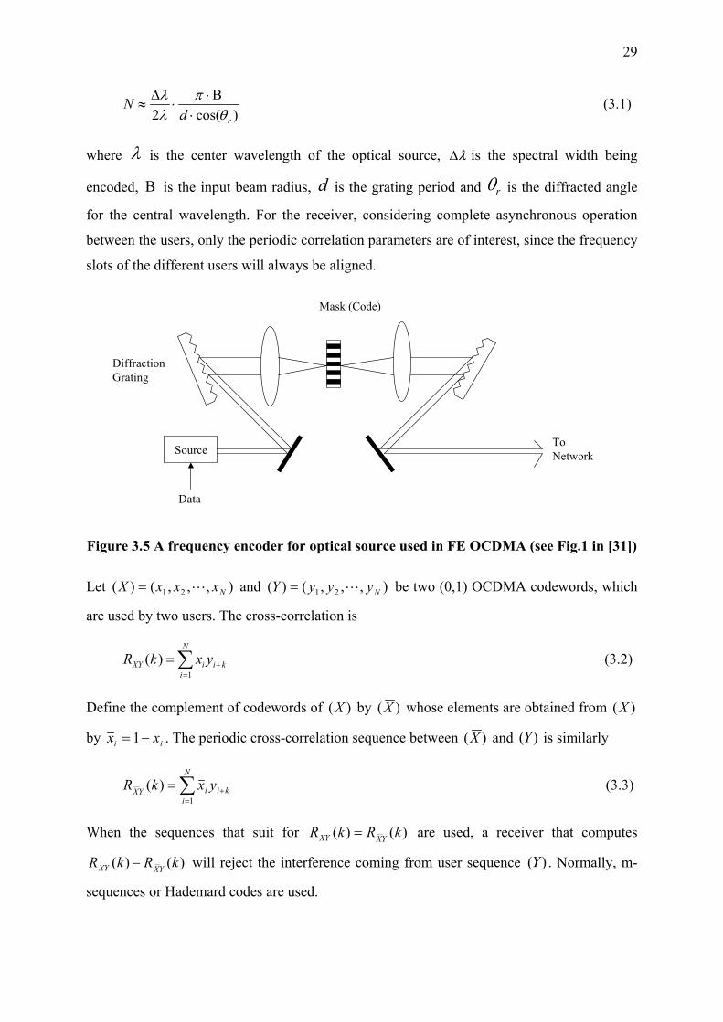
29
)cos(2 rdN
θπ
λλ
⋅Β⋅
⋅∆
≈ (3.1)
where λ is the center wavelength of the optical source, λ∆ is the spectral width being
encoded, is the input beam radius, is the grating period and Β d rθ is the diffracted angle
for the central wavelength. For the receiver, considering complete asynchronous operation
between the users, only the periodic correlation parameters are of interest, since the frequency
slots of the different users will always be aligned.
Source
Data
ToNetwork
DiffractionGrating
Mask (Code)
Figure 3.5 A frequency encoder for optical source used in FE OCDMA (see Fig.1 in [31])
Let and ( be two (0,1) OCDMA codewords, which
are used by two users. The cross-correlation is
),,,()( 21 NxxxX L= ),,,() 21 NyyyY L=
∑=
+=N
ikiiXY yxkR
1)( (3.2)
Define the complement of codewords of by )(X )(X whose elements are obtained from (
by
)X
ii xx −= 1 . The periodic cross-correlation sequence between )(X and ( is similarly )Y
∑=
+=N
ikiiYX yxkR
1)( (3.3)
When the sequences that suit for )()( kRkR YXXY = are used, a receiver that computes
)()( kRkR YXXY − will reject the interference coming from user sequence ( . Normally, m-
sequences or Hademard codes are used.
)Y
30
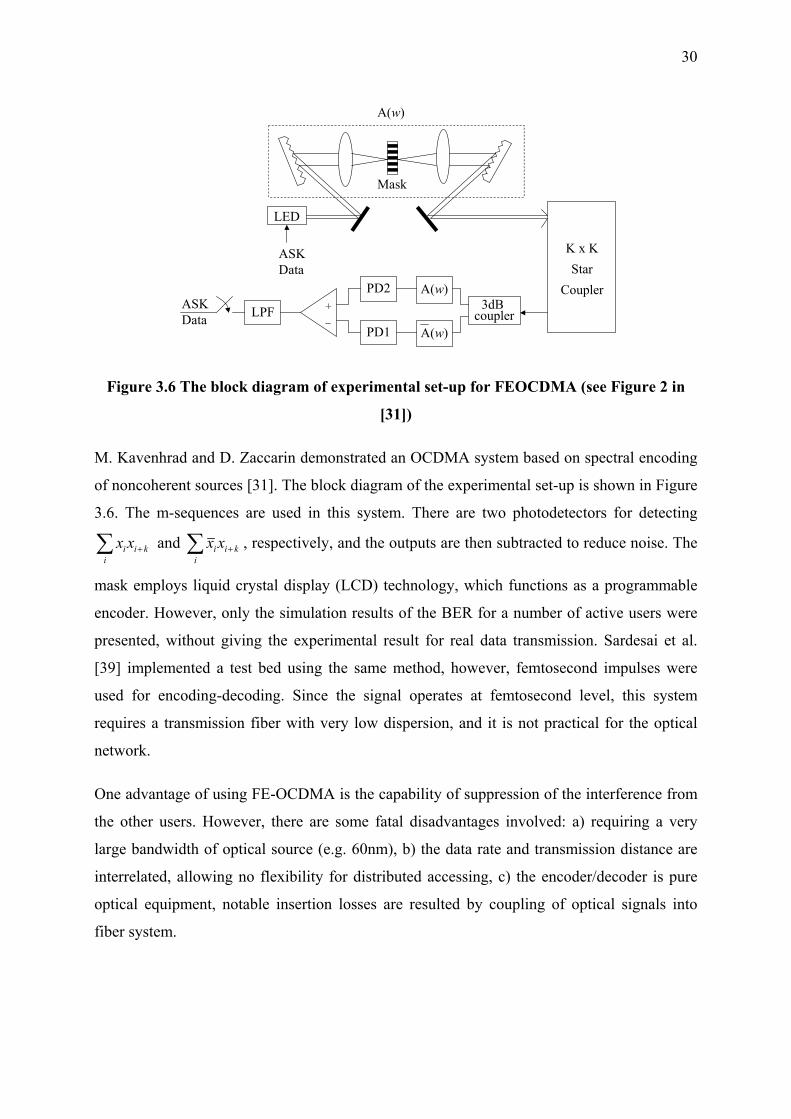
Mask
LED
ASKData
K x KStar
Coupler3dB
coupler
A(w)
A(w)PD1
PD2
LPF +_
ASKData
A(w)
Figure 3.6 The block diagram of experimental set-up for FEOCDMA (see Figure 2 in
[31])
M. Kavenhrad and D. Zaccarin demonstrated an OCDMA system based on spectral encoding
of noncoherent sources [31]. The block diagram of the experimental set-up is shown in Figure
3.6. The m-sequences are used in this system. There are two photodetectors for detecting
and ∑ +i
kii xx ∑ +i
kii xx , respectively, and the outputs are then subtracted to reduce noise. The
mask employs liquid crystal display (LCD) technology, which functions as a programmable
encoder. However, only the simulation results of the BER for a number of active users were
presented, without giving the experimental result for real data transmission. Sardesai et al.
[39] implemented a test bed using the same method, however, femtosecond impulses were
used for encoding-decoding. Since the signal operates at femtosecond level, this system
requires a transmission fiber with very low dispersion, and it is not practical for the optical
network.
One advantage of using FE-OCDMA is the capability of suppression of the interference from
the other users. However, there are some fatal disadvantages involved: a) requiring a very
large bandwidth of optical source (e.g. 60nm), b) the data rate and transmission distance are
interrelated, allowing no flexibility for distributed accessing, c) the encoder/decoder is pure
optical equipment, notable insertion losses are resulted by coupling of optical signals into
fiber system.
31
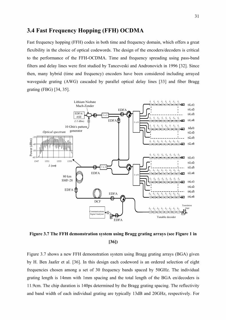
3.4 Fast Frequency Hopping (FFH) OCDMA
Fast frequency hopping (FFH) codes in both time and frequency domain, which offers a great
flexibility in the choice of optical codewords. The design of the encoders/decoders is critical
to the performance of the FFH-OCDMA. Time and frequency spreading using pass-band
filters and delay lines were first studied by Tanceveski and Andronovich in 1996 [32]. Since
then, many hybrid (time and frequency) encoders have been considered including arrayed
waveguide grating (AWG) cascaded by parallel optical delay lines [33] and fiber Bragg
grating (FBG) [34, 35].
Lithium NiobateMach-Zender
10 Gbit/s patterngeneratorOptical spectrum
80 kmSMF-28
EDFA
EDFA
EDFA
EDFA
CommunicationsSignal Analyser
DCF
Tunable decoder
Translation stage
EDFA
EDFA
EDFA/ASE
(3.5 dBm)
1547 1551 1555 1559
)(nmλ
-65
-55
-45
-35
Pow
er (d
Bm
)
1 x 2
1 x 2
1 x 8
1 x 8
511362941 λλλλλλλλ
8146951274 λλλλλλλλ
91571061385 λλλλλλλλ
12181013916118 λλλλλλλλ
131911141017129 λλλλλλλλ
1622141713201512 λλλλλλλλ
2127191218252017 λλλλλλλλ
2430221521282320 λλλλλλλλ
1821261913202822 λλλλλλλλ
Figure 3.7 The FFH demonstration system using Bragg grating arrays (see Figure 1 in
[36])
Figure 3.7 shows a new FFH demonstration system using Bragg grating arrays (BGA) given
by H. Ben Jaafer et al. [36]. In this design each codeword is an ordered selection of eight
frequencies chosen among a set of 30 frequency bands spaced by 50GHz. The individual
grating length is 14mm with 1mm spacing and the total length of the BGA en/decoders is
11.9cm. The chip duration is 140ps determined by the Bragg grating spacing. The reflectivity
and band width of each individual grating are typically 13dB and 20GHz, respectively. For
32
the transmission experiment, amplified spontaneous emission (ASE) of an erbium-doped fiber
amplifier (EDFA) is used as an incoherent broadband source. An electrooptical modulator is
used to generate the data stream forming a pattern generator with 100ps impulse width.
Because only one modulator and one data generator are used, the modulated impulses are split
into 16 encoders by passive components. The encoded signals then propagate through 80km
single mode fiber (SMF) and dispersion compensating fiber (DCF). At the receiver end, the
signal is fed into a strain tunable decoder. The decoded signal, consisting of the sum of the
desired user signal and the interference contribution, is evaluated in a communication signal
analyzer.
FHH-OCDMA system utilizes multiple frequency points, the chip impulses with different
frequencies of optical carriers will travel with different velocities due to the fiber
characteristic, and the relative positions among them will be changed. Consequently, the
decoder cannot correctly recover the desired bit without dispersion compensation, which is
still unusual in LAN. In addition, the utility-rate of the bandwidth of demonstration systems is
much lower than that by using DWDM technology. Furthermore the demonstrated systems
are synchronous, and a narrow frequency band used in FHH-OCDMA codeword is normally
located in a different position for different codewords. When the number of users increases,
the interferometric noise increases which is caused by the overlap of two beams having the
same frequency, similarly as in DS-OCDMA system.
3.5 PSK-OCDMA
With the developments of the fiber Bragg grating technology and planar lightwave circuit
(PLC), it is possible to use the optical phase for coding. A series of experiments of
BPSK/QPSK OCDMA have been carried out at University of Southampton in UK [40, 41].
Strain-tunable fiber Bragg gratings (called superstructured fiber Bragg gratings (SSFBG)
were used as phase encoder/decoders. SSFBG is a single-grating structure having a slowly
varying amplitude and/or a phase pattern (superstructure) imposed upon a uniform
background refractive index modulation. In the weak grating limit (reflectivity < 20%), the
shape of the impulse responses are directly following the shape of the spatial superstructure.
Thus, OCDMA codes can be written directly into SSFBG, such that short impulses reflected
from the structure are shaped into the codewords. Quaternary phase coding with code length
of 255 chips and chip rate of 320Gchip/s is demonstrated [40]. A typical experimental set-up
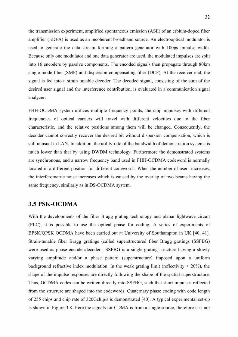
is shown in Figure 3.8. Here the signals for CDMA is from a single source, therefore it is not
33
sure if the result is the same as for two or more signal sources. Because when the signal
source is the same, the signal pattern of each channel is also the same, therefore there is no
noise from other channels at the same wavelength if a Null is transmitted.
Wavelength Converter
EDFAMOD
1.25 Gbit/s Data in 255-chip QPSK SSFBGs,1λ
Q1
Q2
B3
B4
EDFA
Q1*
Diagnostics
255-chip QPSK SSFBGs,1λ
EDFAEDFA
EDFA
Filter
63-chip BPSK SSFBGs
CW Laser1556.5 nm
1λ
2λ
EFRL1552.5nm10 GHz
,2λ
Figure 3.8 The system using superstructured fiber Bragg gratings (see Figure 3 in [40])
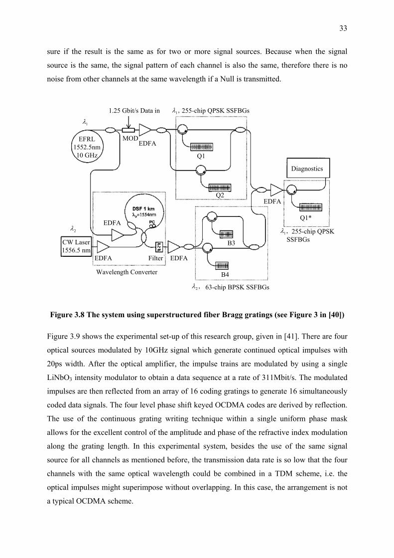
Figure 3.9 shows the experimental set-up of this research group, given in [41]. There are four
optical sources modulated by 10GHz signal which generate continued optical impulses with
20ps width. After the optical amplifier, the impulse trains are modulated by using a single
LiNbO3 intensity modulator to obtain a data sequence at a rate of 311Mbit/s. The modulated
impulses are then reflected from an array of 16 coding gratings to generate 16 simultaneously
coded data signals. The four level phase shift keyed OCDMA codes are derived by reflection.
The use of the continuous grating writing technique within a single uniform phase mask
allows for the excellent control of the amplitude and phase of the refractive index modulation
along the grating length. In this experimental system, besides the use of the same signal
source for all channels as mentioned before, the transmission data rate is so low that the four
channels with the same optical wavelength could be combined in a TDM scheme, i.e. the
optical impulses might superimpose without overlapping. In this case, the arrangement is not
a typical OCDMA scheme.
34
DFB FiberLaser
1567.32 nm
DFB FiberLaser
1548.11 nm
TunableLaser
1548.91 nm
DFB FiberLaser
1548.11 nm
10 GHzClock
EAM
EDFA EDFAMOD
311 Mbit/SData
Q1
Q2
Q3
Q4
A
C
B
Wavelength (nm)
Wavelength (nm)1546 1547 1548 1549 1550 1551
155115501549154815471546 1546 1547 1548 15491549 1550 1551
Wavelength (nm)
B
C
A
Strain tunable Q1*
BERT
Strain tunableQ2*
BERT
BERT
BERT
StraintunableQ3*
Strain tunable Q4*
EDFA EDFA
50km SMF-28
fiber
Pow
er (1
0 dB
/div
)Po
wer
(10
dB/d
iv)
Pow
er (1
0 dB
/div
)
4321 λλλλ
4321 λλλλ
4321 λλλλ
4321 λλλλ 41 ~ λλ
41 ~ λλ
41 ~ λλ
41 ~ λλ
Figure 3.9 The 16 channels OCDMA system using SSFBG (see Figure 1 in [41])
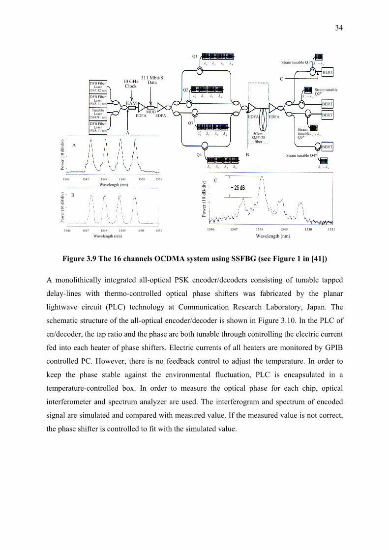
A monolithically integrated all-optical PSK encoder/decoders consisting of tunable tapped
delay-lines with thermo-controlled optical phase shifters was fabricated by the planar
lightwave circuit (PLC) technology at Communication Research Laboratory, Japan. The
schematic structure of the all-optical encoder/decoder is shown in Figure 3.10. In the PLC of
en/decoder, the tap ratio and the phase are both tunable through controlling the electric current
fed into each heater of phase shifters. Electric currents of all heaters are monitored by GPIB
controlled PC. However, there is no feedback control to adjust the temperature. In order to
keep the phase stable against the environmental fluctuation, PLC is encapsulated in a
temperature-controlled box. In order to measure the optical phase for each chip, optical
interferometer and spectrum analyzer are used. The interferogram and spectrum of encoded
signal are simulated and compared with measured value. If the measured value is not correct,
the phase shifter is controlled to fit with the simulated value.
35
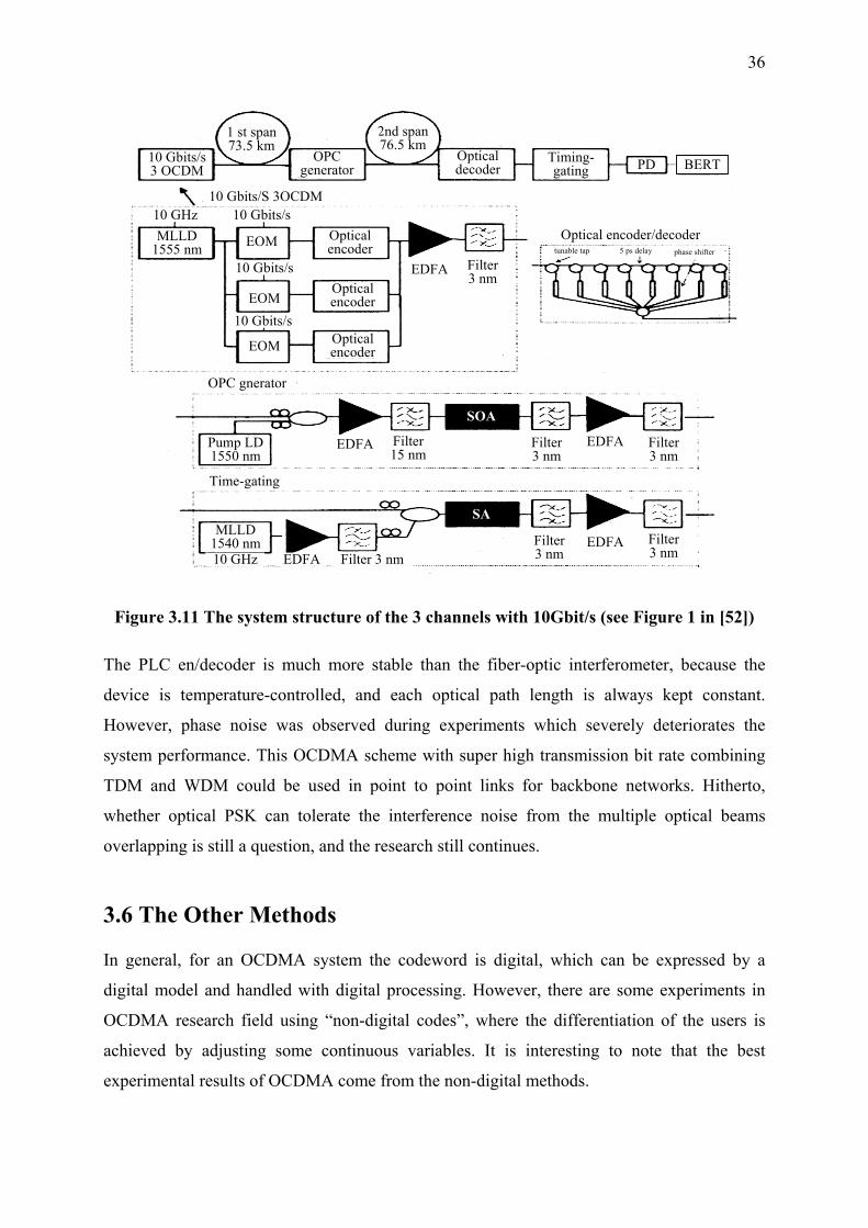
Figure 3.10 The schematic structure of the all-optical en/decoder (see Fig. 6 in [51])
The typical scheme using this component (or equipment) in OCDMA system is presented in
[53]. The system setup is show in Figure 3.11. A 10GHz repetition rate, 2.0ps impulse stream
at 1555nm is generated by a hybrid mode locked semiconductor Laserdiode (MLLD). It is
divided into three impulse streams and each of them is externally modulated using a 10Gbit/s
pseudo-random bit stream. The taps of the encoder are tuned so that they split i nto an eight-
impulse sequence with equal amplitude. The carrier phase of each tapped impulse is binary
changed by 0 or π . Then an optical code of 8-chip BPSK impulse sequence with a chip
interval of 5ps is generated. After dispersion compensated transmission, the optical decoder
with the same structured matched filters receives the signals in the time domain, followed by
time-gating. In [52] the camera traces of the three combined signals have not been given,
therefore, whether the decoded signal is disturbed by other two signals remains unknown.
Since the duration of one data bit is 100ps, and an encoded bit only occupies 40ps, it is
possible that the desired signal isn’ t disturbed by other signals. Thus the system did not
explicitl y demonstrate the MAI in PSK-OCDMA. It is claimed by the same researchers in
[42] and [43] that a 160Gbit/s OCDMA/WDM (10Gbit/s 4CDMA 4WDM) transmission
with a novel side-lobes suppression detection transmission and a 6.4Tbit/s OCDM/WDM
(4OCDM 40WDM 40Gbit/s) transmission were achieved. However, by using a system
with only one signal source for all CDMA users and WDM channels, the above mentioned
results are unlikely.
36
EDFA
1 st span73.5 km
10 Gbits/s3 OCDM
Optical encoder/decoder
OPCgenerator
2nd span76.5 km
Opticaldecoder
Opticalencoder
Timing-gating PD BERT
phase shiftertunable tap 5 ps delay
OpticalencoderOpticalencoder
Opticalencoder
10 Gbits/s
EOM
EOM
EOM
10 Gbits/s
10 Gbits/s
10 GHz
Filter3 nm
MLLD1555 nm
OPC gnerator
10 Gbits/S 3OCDM
Pump LD1550 nm
MLLD1540 nm
Filter3 nm
EDFA Filter3 nm
Filter3 nm
Filter3 nm
EDFA
Filter15 nm
EDFA
EDFA Filter 3 nm10 GHz
Time-gating
SOA
SA
Figure 3.11 The system structure of the 3 channels with 10Gbit/s (see Figure 1 in [52])
The PLC en/decoder is much more stable than the fiber-optic interferometer, because the
device is temperature-controlled, and each optical path length is always kept constant.
However, phase noise was observed during experiments which severely deteriorates the
system performance. This OCDMA scheme with super high transmission bit rate combining
TDM and WDM could be used in point to point links for backbone networks. Hitherto,
whether optical PSK can tolerate the interference noise from the multiple optical beams
overlapping is still a question, and the research still continues.
3.6 The Other Methods
In general, for an OCDMA system the codeword is digital, which can be expressed by a
digital model and handled with digital processing. However, there are some experiments in
OCDMA research field using “non-digital codes”, where the differentiation of the users is
achieved by adjusting some continuous variables. It is interesting to note that the best
experimental results of OCDMA come from the non-digital methods.
37
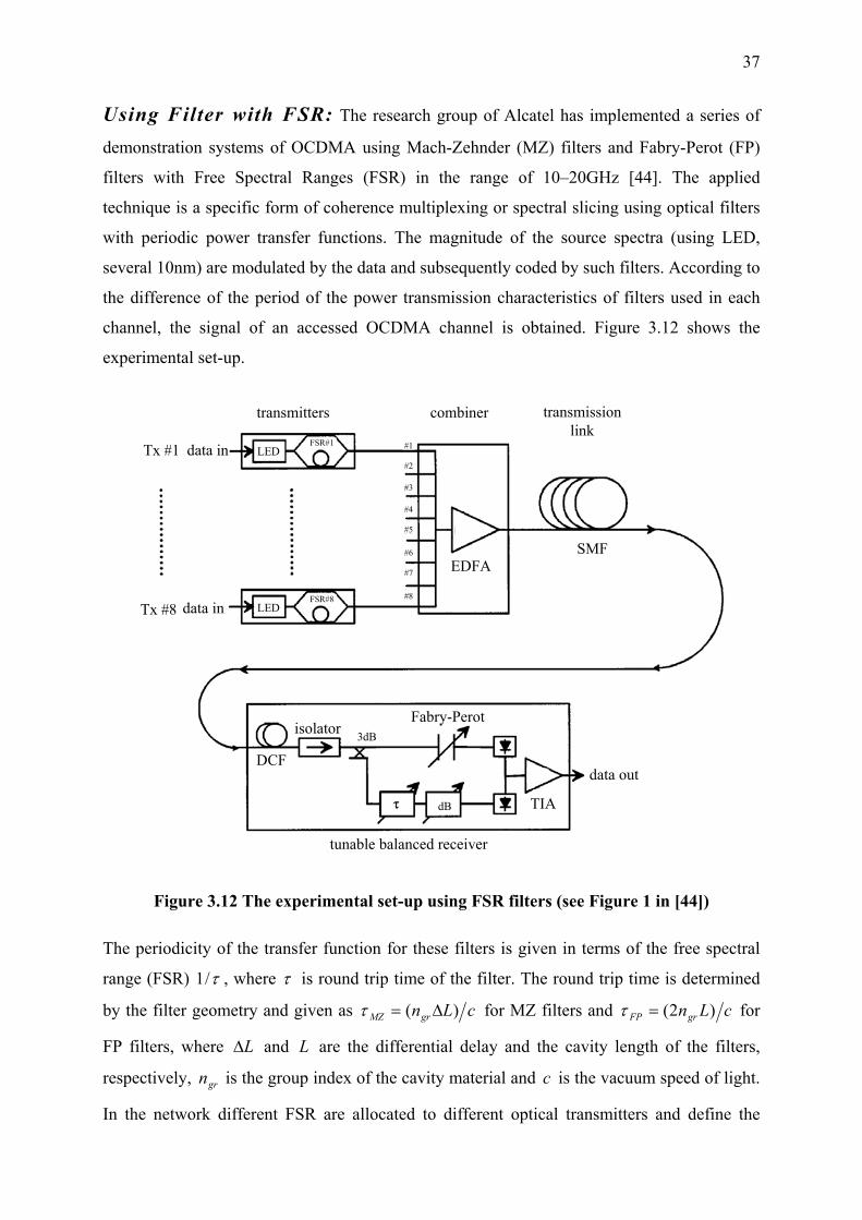
Using Filter with FSR: The research group of Alcatel has implemented a series of
demonstration systems of OCDMA using Mach-Zehnder (MZ) filters and Fabry-Perot (FP)
filters with Free Spectral Ranges (FSR) in the range of 10–20GHz [44]. The applied
technique is a specific form of coherence multiplexing or spectral slicing using optical filters
with periodic power transfer functions. The magnitude of the source spectra (using LED,
several 10nm) are modulated by the data and subsequently coded by such filters. According to
the difference of the period of the power transmission characteristics of filters used in each
channel, the signal of an accessed OCDMA channel is obtained. Figure 3.12 shows the
experimental set-up.
combiner transmissionlink
EDFASMF
data in
data inTx #1
Tx #8 LED
LEDFSR#1
FSR#8
#1
#2
#3
#4
#5
#6
#7
#8
DCF
isolator 3dBFabry-Perot
TIAdB
data out
tunable balanced receiver
transmitters
Figure 3.12 The experimental set-up using FSR filters (see Figure 1 in [44])
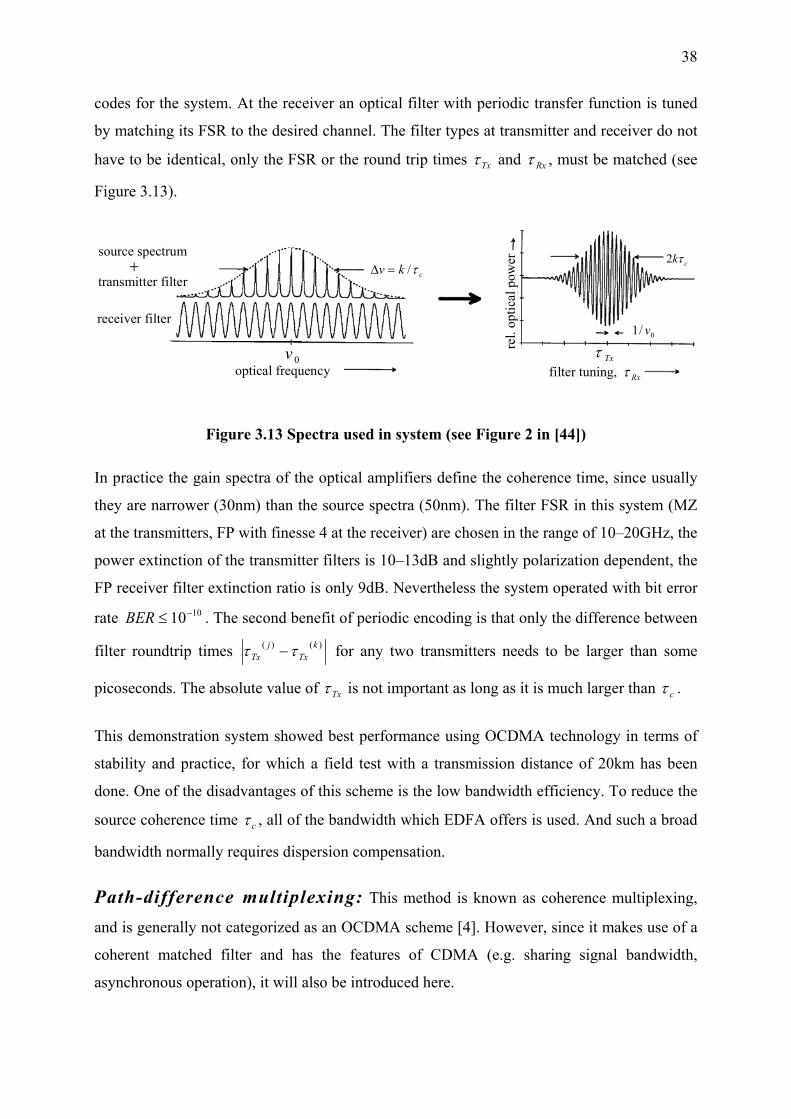
The periodicity of the transfer function for these filters is given in terms of the free spectral
range (FSR) τ/1 , where τ is round trip time of the filter. The round trip time is determined
by the filter geometry and given as cLngrMZ )( ∆=τ for MZ filters and cLngrFP )2(=τ for
FP filters, where and are the differential delay and the cavity length of the filters,
respectively, is the group index of the cavity material and is the vacuum speed of light.
In the network different FSR are allocated to different optical transmitters and define the
L∆ L
grn c
38
codes for the system. At the receiver an optical filter with periodic transfer function is tuned
by matching its FSR to the desired channel. The filter types at transmitter and receiver do not
have to be identical, only the FSR or the round trip times Txτ and Rxτ , must be matched (see
Figure 3.13).
ckτ2
Txτfilter tuning,
0/1 v
transmitter filter
receiver filter
+source spectrum
optical frequency0v
ckv τ/=∆
Rxτ
rel.
optic
al p
ower
Figure 3.13 Spectra used in system (see Figure 2 in [44])
In practice the gain spectra of the optical amplifiers define the coherence time, since usually
they are narrower (30nm) than the source spectra (50nm). The filter FSR in this system (MZ
at the transmitters, FP with finesse 4 at the receiver) are chosen in the range of 10–20GHz, the
power extinction of the transmitter filters is 10–13dB and slightly polarization dependent, the
FP receiver filter extinction ratio is only 9dB. Nevertheless the system operated with bit error
rate . The second benefit of periodic encoding is that only the difference between
filter roundtrip times
1010−≤BER)()( k
Txj
Tx ττ − for any two transmitters needs to be larger than some
picoseconds. The absolute value of Txτ is not important as long as it is much larger than cτ .
This demonstration system showed best performance using OCDMA technology in terms of
stability and practice, for which a field test with a transmission distance of 20km has been
done. One of the disadvantages of this scheme is the low bandwidth efficiency. To reduce the
source coherence time cτ , all of the bandwidth which EDFA offers is used. And such a broad
bandwidth normally requires dispersion compensation.
Path-difference multiplexing: This method is known as coherence multiplexing,
and is generally not categorized as an OCDMA scheme [4]. However, since it makes use of a
coherent matched filter and has the features of CDMA (e.g. sharing signal bandwidth,
asynchronous operation), it will also be introduced here.
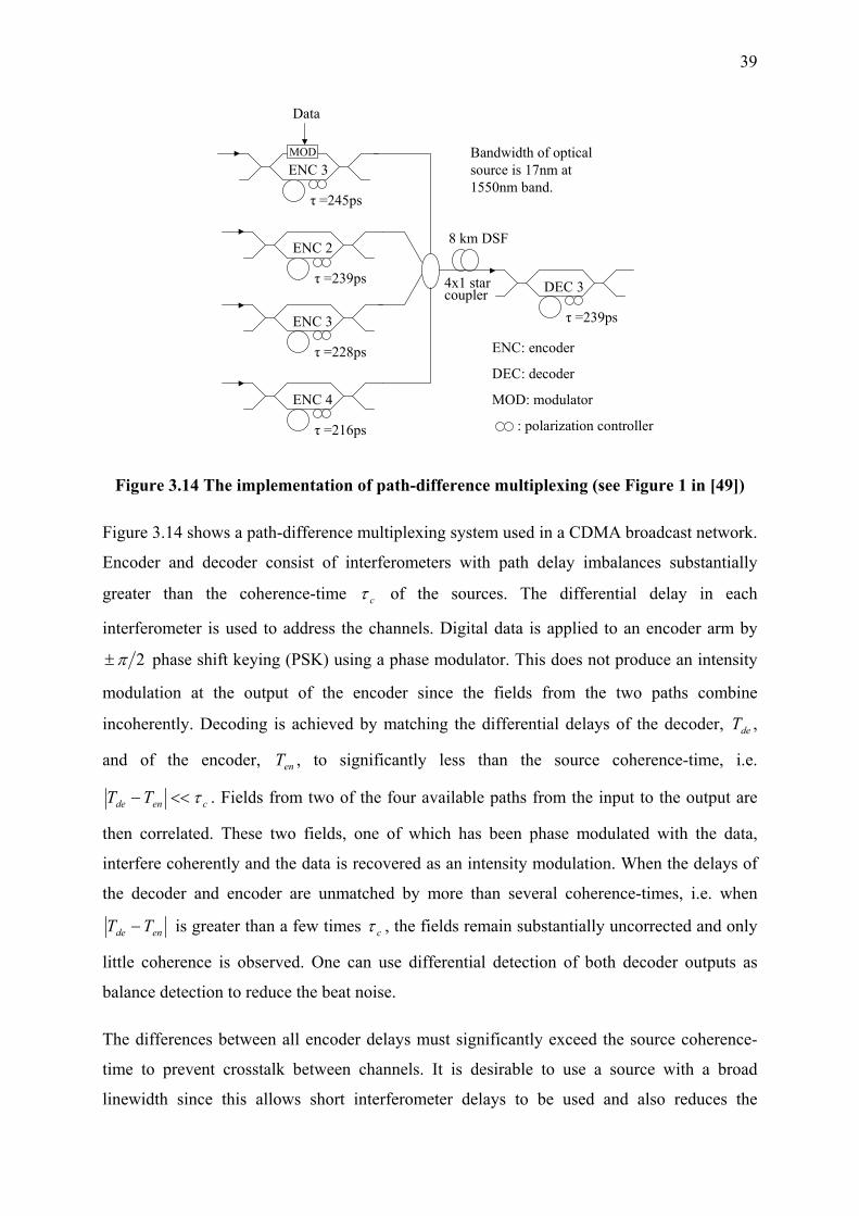
39
τ =239ps
τ =228ps
ENC 3
τ =216ps
ENC 4
ENC 2
τ =245ps
ENC 3
τ =239ps
DEC 3
MOD
Data
4x1 starcoupler
Bandwidth of opticalsource is 17nm at1550nm band.
8 km DSF
ENC: encoder
DEC: decoder
MOD: modulator
: polarization controller
Figure 3.14 The implementation of path-difference multiplexing (see Figure 1 in [49])
Figure 3.14 shows a path-difference multiplexing system used in a CDMA broadcast network.
Encoder and decoder consist of interferometers with path delay imbalances substantially
greater than the coherence-time cτ of the sources. The differential delay in each
interferometer is used to address the channels. Digital data is applied to an encoder arm by
2π± phase shift keying (PSK) using a phase modulator. This does not produce an intensity
modulation at the output of the encoder since the fields from the two paths combine
incoherently. Decoding is achieved by matching the differential delays of the decoder, T ,
and of the encoder, T , to significantly less than the source coherence-time, i.e.
de
en
cende TT τ<<− . Fields from two of the four available paths from the input to the output are
then correlated. These two fields, one of which has been phase modulated with the data,
interfere coherently and the data is recovered as an intensity modulation. When the delays of
the decoder and encoder are unmatched by more than several coherence-times, i.e. when
ende TT − is greater than a few times cτ , the fields remain substantially uncorrected and only
little coherence is observed. One can use differential detection of both decoder outputs as
balance detection to reduce the beat noise.
The differences between all encoder delays must significantly exceed the source coherence-
time to prevent crosstalk between channels. It is desirable to use a source with a broad
linewidth since this allows short interferometer delays to be used and also reduces the
40
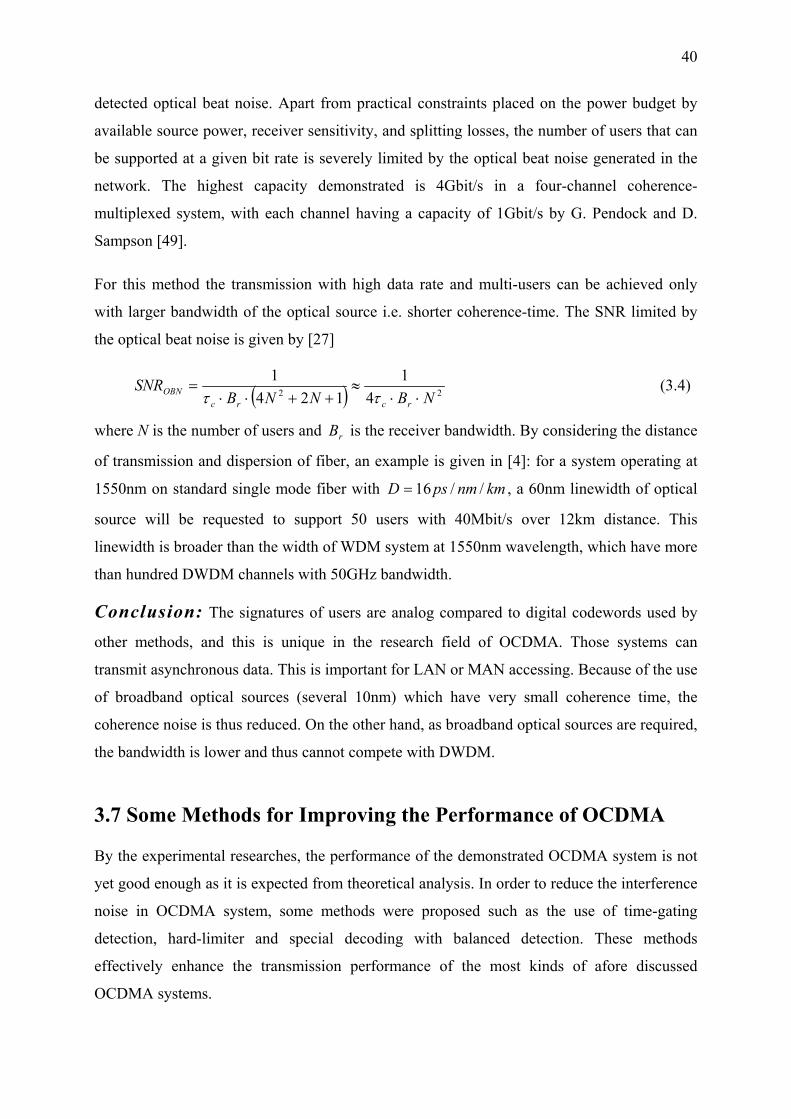
detected optical beat noise. Apart from practical constraints placed on the power budget by
available source power, receiver sensitivity, and splitting losses, the number of users that can
be supported at a given bit rate is severely limited by the optical beat noise generated in the
network. The highest capacity demonstrated is 4Gbit/s in a four-channel coherence-
multiplexed system, with each channel having a capacity of 1Gbit/s by G. Pendock and D.
Sampson [49].
For this method the transmission with high data rate and multi-users can be achieved only
with larger bandwidth of the optical source i.e. shorter coherence-time. The SNR limited by
the optical beat noise is given by [27]
( ) 22 41
1241
NBNNBSNR
rcrcOBN ⋅⋅
≈++⋅⋅
=ττ
(3.4)
where N is the number of users and is the receiver bandwidth. By considering the distance
of transmission and dispersion of fiber, an example is given in [4]: for a system operating at
1550nm on standard single mode fiber with
rB
kmnmpsD //16= , a 60nm linewidth of optical
source will be requested to support 50 users with 40Mbit/s over 12km distance. This
linewidth is broader than the width of WDM system at 1550nm wavelength, which have more
than hundred DWDM channels with 50GHz bandwidth.
Conclusion: The signatures of users are analog compared to digital codewords used by
other methods, and this is unique in the research field of OCDMA. Those systems can
transmit asynchronous data. This is important for LAN or MAN accessing. Because of the use
of broadband optical sources (several 10nm) which have very small coherence time, the
coherence noise is thus reduced. On the other hand, as broadband optical sources are required,
the bandwidth is lower and thus cannot compete with DWDM.
3.7 Some Methods for Improving the Performance of OCDMA
By the experimental researches, the performance of the demonstrated OCDMA system is not
yet good enough as it is expected from theoretical analysis. In order to reduce the interference
noise in OCDMA system, some methods were proposed such as the use of time-gating
detection, hard-limiter and special decoding with balanced detection. These methods
effectively enhance the transmission performance of the most kinds of afore discussed
OCDMA systems.
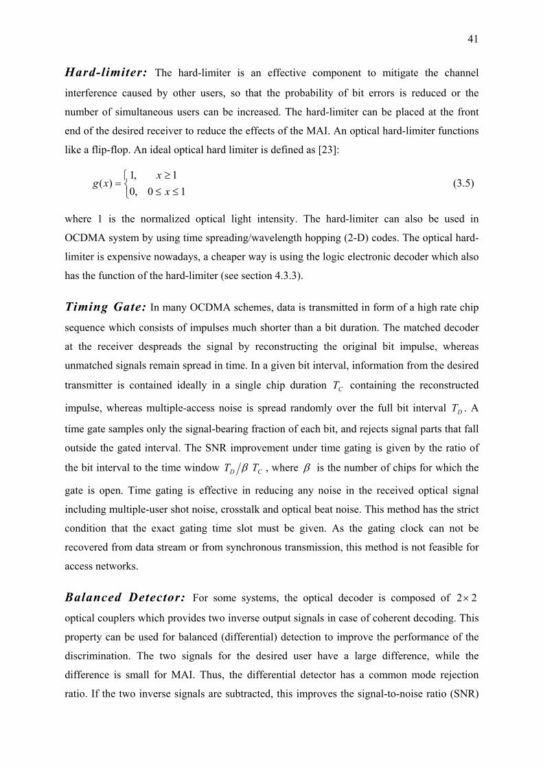
41
Hard-limiter: The hard-limiter is an effective component to mitigate the channel
interference caused by other users, so that the probability of bit errors is reduced or the
number of simultaneous users can be increased. The hard-limiter can be placed at the front
end of the desired receiver to reduce the effects of the MAI. An optical hard-limiter functions
like a flip-flop. An ideal optical hard limiter is defined as [23]:
≤≤≥
=10,0
1,1)(
xx
xg (3.5)
where 1 is the normalized optical light intensity. The hard-limiter can also be used in
OCDMA system by using time spreading/wavelength hopping (2-D) codes. The optical hard-
limiter is expensive nowadays, a cheaper way is using the logic electronic decoder which also
has the function of the hard-limiter (see section 4.3.3).
Timing Gate: In many OCDMA schemes, data is transmitted in form of a high rate chip
sequence which consists of impulses much shorter than a bit duration. The matched decoder
at the receiver despreads the signal by reconstructing the original bit impulse, whereas
unmatched signals remain spread in time. In a given bit interval, information from the desired
transmitter is contained ideally in a single chip duration T containing the reconstructed
impulse, whereas multiple-access noise is spread randomly over the full bit interval T . A
time gate samples only the signal-bearing fraction of each bit, and rejects signal parts that fall
outside the gated interval. The SNR improvement under time gating is given by the ratio of
the bit interval to the time window
C
D
CD TT β , where β is the number of chips for which the
gate is open. Time gating is effective in reducing any noise in the received optical signal
including multiple-user shot noise, crosstalk and optical beat noise. This method has the strict
condition that the exact gating time slot must be given. As the gating clock can not be
recovered from data stream or from synchronous transmission, this method is not feasible for
access networks.
Balanced Detector: For some systems, the optical decoder is composed of 22×
optical couplers which provides two inverse output signals in case of coherent decoding. This
property can be used for balanced (differential) detection to improve the performance of the
discrimination. The two signals for the desired user have a large difference, while the
difference is small for MAI. Thus, the differential detector has a common mode rejection
ratio. If the two inverse signals are subtracted, this improves the signal-to-noise ratio (SNR)
42
by canceling optical beat noise. The level of achieved cancellation depends on the common-
mode rejection ratio of the balanced receiver. This method is often sufficient to remove the
error rate floor, allowing operation at low BER. For the optical method described in sections
3.2 and 3.6, a balanced detector can be used to enhance the performance of systems [49, 46,
38].
3.8 Conclusion
The investigations carried out so far indicate that the technologies for constructing a practical
OCDMA system are far from mature and are eventually more complex than those required for
TDM or WDM systems. Some barriers limiting the realization of OCDMA cannot be
completely solved in the near future. The motivation of introducing OCDMA in optical access
network is that it would allow a more flexible networks structure and introduce the high-speed
optical signal processing in the optical network [7]. For these reasons several researchers have
been exploring the possibility to utilize fiber bandwidth beyond the limits of electronics speed
for purposes of increased network flexibility and decreased access cost.
Table 3.1 The characteristics of various OCDMA proposals
Incoherent
Direct
Sequence
Coherent
Direct
Sequence
Frequency
Coded
OCDMA
Fast
Frequency
Hopping
Phase
Shift
Keying
FSR
Filter
OCDMA
Coherence
Multiplex
OCDMA
Bandwidth requirement Wide Wide Wide Wide
Dispersion impact √ √ √ √
Bandwidth efficiency Low Low low Low
Channels Multi Single Single Multi 2 5 4 Results of
Experiment Data rate
per
channel
10Gbit/s 155
Mbit/s
1Gbit/s
But as shown in Table 3.1, the goals have been only partially achieved up to now. After more
than a decade of research on OCDMA, it is still in the theoretical level. The development in
this area depends more on the evolution of other relative technology. Except the early lower
43
bit rate demonstration system [6], the problem of the interferometric noise was evaded for all
the experiments of CDMA with optical en/decoding process.
Obviously, the use of OCDMA with all optical en/decoding process in access network is still
difficult up to now. However, the method using electronic en/decoding process to achieve
CDMA in optical channel is a promising choice which can provide a good performance with
narrow bandwidth in optical access network. In chapter 4, the feasibility of OCDMA with the
electronic en/decoding process will be discussed, and the experiments with such a system will
be presented in chapter 5.
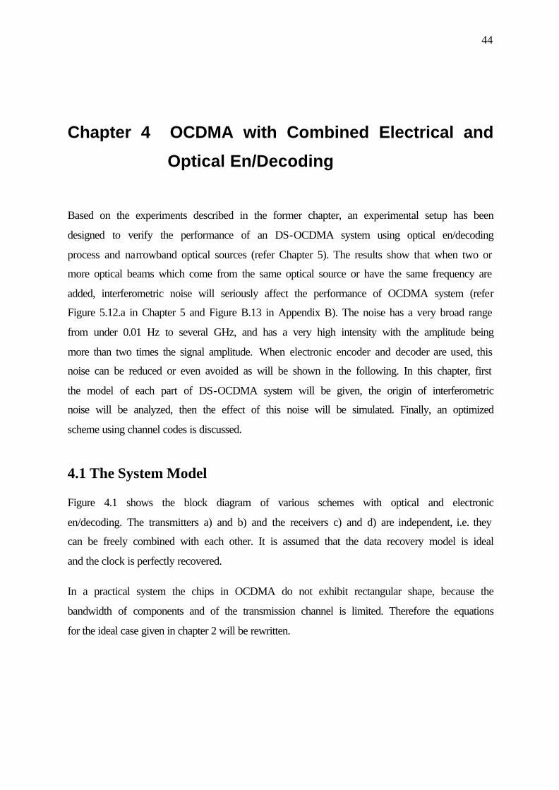
44
Chapter 4 OCDMA with Combined Electrical and
Optical En/Decoding
Based on the experiments described in the former chapter, an experimental setup has been
designed to verify the performance of an DS-OCDMA system using optical en/decoding
process and narrowband optical sources (refer Chapter 5). The results show that when two or
more optical beams which come from the same optical source or have the same frequency are
added, interferometric noise will seriously affect the performance of OCDMA system (refer
Figure 5.12.a in Chapter 5 and Figure B.13 in Appendix B). The noise has a very broad range
from under 0.01 Hz to several GHz, and has a very high intensity with the amplitude being
more than two times the signal amplitude. When electronic encoder and decoder are used, this
noise can be reduced or even avoided as will be shown in the following. In this chapter, first
the model of each part of DS-OCDMA system will be given, the origin of interferometric
noise will be analyzed, then the effect of this noise will be simulated. Finally, an optimized
scheme using channel codes is discussed.
4.1 The System Model
Figure 4.1 shows the block diagram of various schemes with optical and electronic
en/decoding. The transmitters a) and b) and the receivers c) and d) are independent, i.e. they
can be freely combined with each other. It is assumed that the data recovery model is ideal
and the clock is perfectly recovered.
In a practical system the chips in OCDMA do not exhibit rectangular shape, because the
bandwidth of components and of the transmission channel is limited. Therefore the equations
for the ideal case given in chapter 2 will be rewritten.
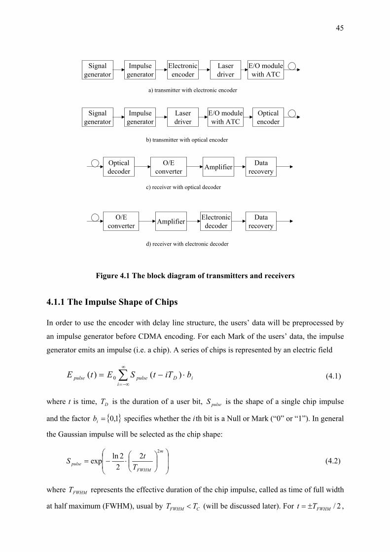
45
a) transmitter with electronic encoder
b) transmitter with optical encoder
Signalgenerator
Impulsegenerator
Electronicencoder
Laserdriver
E/O modulewith ATC
Signalgenerator
Impulsegenerator
Opticalencoder
Laserdriver
E/O modulewith ATC
Amplifier Datarecovery
Opticaldecoder
O/Econverter
c) receiver with optical decoder
Amplifier Datarecovery
Electronicdecoder
O/Econverter
d) receiver with electronic decoder
Figure 4.1 The block diagram of transmitters and receivers
4.1.1 The Impulse Shape of Chips
In order to use the encoder with delay line structure, the users’ data will be preprocessed by
an impulse generator before CDMA encoding. For each Mark of the users’ data, the impulse
generator emits an impulse (i.e. a chip). A series of chips is represented by an electric field
∑∞
−∞=
⋅−=i
iDpulsepulse biTtSEtE )()( 0 (4.1)
where t is time, T is the duration of a user bit, is the shape of a single chip impulse
and the factor b specifies whether the i th bit is a Null or Mark (“0” or “1”). In general
the Gaussian impulse will be selected as the chip shape:
D
=
pulseS
1,0i
⋅−=
m
FWHMpulse T
tS2
222lnexp (4.2)
where T represents the effective duration of the chip impulse, called as time of full width
at half maximum (FWHM), usual by T
FWHM
CFWHM T< (will be discussed later). For t , 2/FWHMT±=
46
the power is half of its maximum value. m denotes the order of the super-Gaussian function.
Here we set m=1, so that the chip shape is similar to the practical chip shape in our
experimental system. Then Eq. (4.2) is simplified as
⋅−=
22
22lnexp
FWHMpulse T
tS (4.3)
The chip shape with T is given in Figure 4.2. Note that the duration of is
unlimited.
nsFWHM 3.0= pulseS
-1 -0.5 0 0.5 1 1.50
0.1
0.2
0.3
0.4
0.5
0.6
0.7
0.8
0.9
1
S pul
se(t)
Time ns
Figure 4.2 The shape of the impulse in Eq. (4.3) with T =0.3ns FWHM
4.1.2 Electronic Encoder
We assume that in an OCDMA encoder with delay line structure the shape of each chip is the
same. Therefore when input is , the output of the electronic encoder is pulseE
( ) li
L
l iFWHMCD
L
llCpulseecode
cbTlTiTtE
clTtEtE
C
C
⋅⋅
−−⋅−=
⋅−=
∑ ∑
∑−
=
∞
−∞=
−
=
1
0
20
1
0
/)(222lnexp
)()( (4.4)
where T is the chip duration in OCDMA system, TC CDC LT /= , where is the length of the
codeword. The factor c specifies whether the l th chip is a Null or Mark in a
codeword.
CL
1,0=l
47
4.1.3 Optical Modulator
The electronic signal will be converted into an optical signal. Because the electric/optical
converter requires a large current to drive the Laserdiode, a driver must be used to obtain a
suitable powerful current. In order to set up the operating point for the Laserdiode, the
maximum and minimum current must be adjustable. Normally, the transfer function is linear
and the driver output current is
bi ItEKtI +⋅= )()( (4.5)
where is the bias current for suppressing the transient phenomena of the Laserdiode, K is
the conversion coefficient and is the input signal of the driver.
bI
)(tEi
DFB laser modulator, electro-absorption modulator (EAM) and the Mach-Zehnder modulator
are available to be used in such a high speed optical transmission system. In the experiment
we used the first two types of optical modulator which will be discussed here.
DFB laser: The scheme of the laser model is shown in Figure 4.3 [71]. It contains a white
noise source ω∆ with a deviation of f∆π2 corresponding to the optical laser linewidth f∆ .
The output of the DFB Laserdiode is a time dependent field . The electrical field of the
optical output is therefore determined by
)(tEM
( ) ( )( )( ) ( )( ) ( )( ) ( )
+−++⋅
−= ∫ ττω
τπ
τπδτ
τδαωδ
dIPK
IPKItjek
ktIPtEt
sppjM
0
'2
2ln2
exp1)()(
(4.6)
where α is the linewidth enhancement factor and δ is the additional phase. is the
conversion function given by the I-P curve of the DFB laser and it depends on the character of
the laser. The simplified function can be given as
))(( tIP
( )( )th
th
th ItIifItIif
IatIbtIa
tIP≥<
⋅+⋅⋅
=)()(
,)(),(
(4.7)
where a, b are the coefficients of the converter efficiency before and after the stimulated
emission of the Laserdiode, respectively, ba <<<0 for high speed laser. is the threshold
current of the Laserdiode, and is the power at laser threshold. The first term of the
integrand in Eq. (4.6),
thI
thIa ⋅
ttI
δδ )))((ln( , specifies the dynamic chirp, the other two terms specify
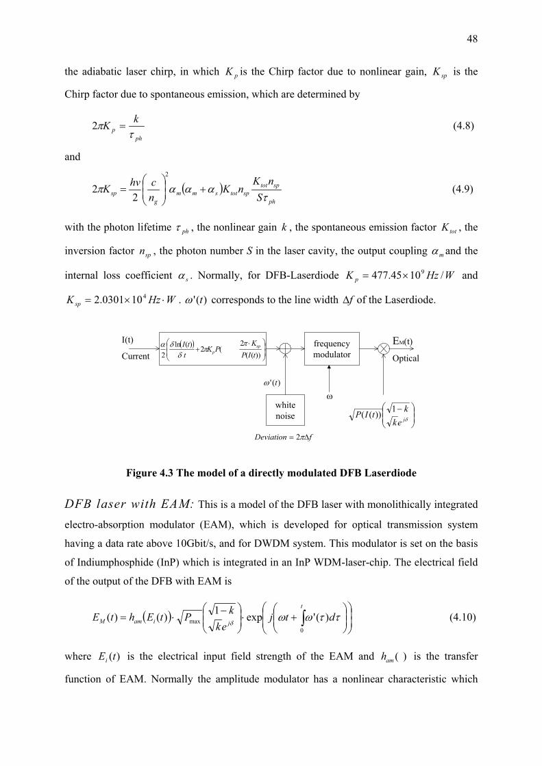
48
the adiabatic laser chirp, in which is the Chirp factor due to nonlinear gain, is the
Chirp factor due to spontaneous emission, which are determined by
pK spK
totnK
K
mα
WHz /
−))(tI
−jekδ
php
kKτ
π =2 (4.8)
and
( )ph
sptotspsmm
gsp S
nKnchvK
ταααπ +
=
2
22 (4.9)
with the photon lifetime phτ , the nonlinear gain , the spontaneous emission factor , the
inversion factor n , the photon number S in the laser cavity, the output coupling
k tot
sp and the
internal loss coefficient sα . Normally, for DFB-Laserdiode and
.
K p 1045.477 9×=
WK sp ⋅×= 0301.2 Hz410 )(' tω corresponds to the line width f∆ of the Laserdiode.
frequencymodulator
whitenoise
I(t)
CurrentEM(t)
Optical
ω
( )
⋅+
))((2
(2)(ln2 tIP
KPK
ttI sp
p
ππ
δδα
−δjekktIP 1))((
)(' tω
fDeviation ∆= π2
Figure 4.3 The model of a directly modulated DFB Laserdiode
DFB laser with EAM: This is a model of the DFB laser with monolithically integrated
electro-absorption modulator (EAM), which is developed for optical transmission system
having a data rate above 10Gbit/s, and for DWDM system. This modulator is set on the basis
of Indiumphosphide (InP) which is integrated in an InP WDM-laser-chip. The electrical field
of the output of the DFB with EAM is
( )
+⋅
⋅= ∫
t
iamM dtjk
PtEhtE0
max )('exp1)()( ττωω (4.10)
where is the electrical input field strength of the EAM and is the transfer
function of EAM. Normally the amplitude modulator has a nonlinear characteristic which
)(tEi )(amh
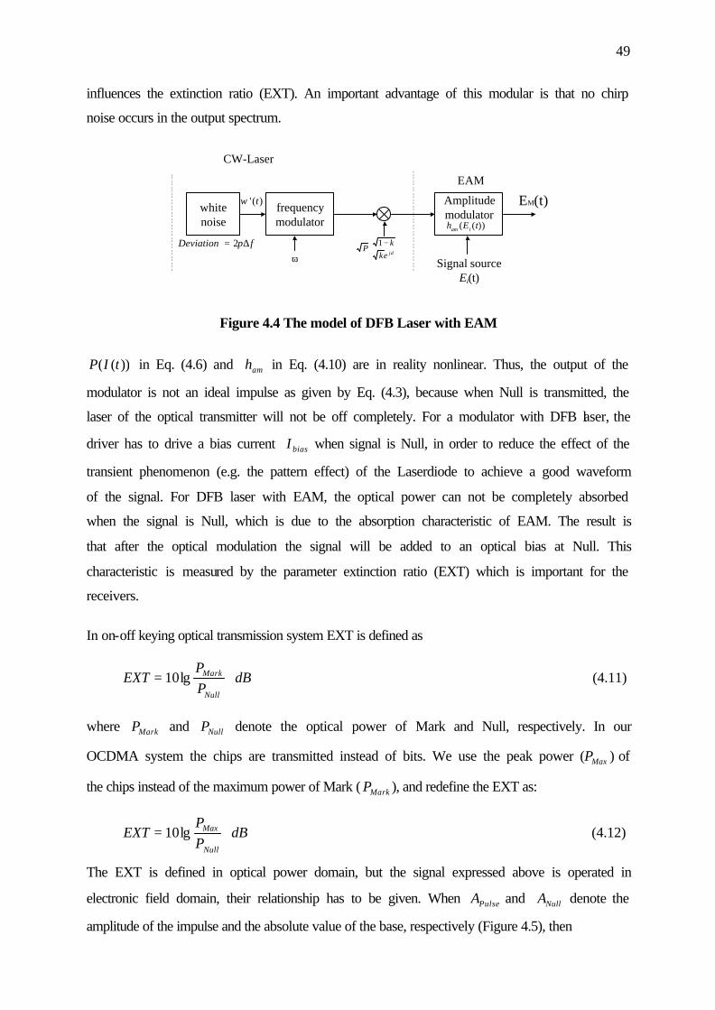
49
influences the extinction ratio (EXT). An important advantage of this modular is that no chirp
noise occurs in the output spectrum.
Amplitudemodulator
Signal sourceEi(t)
whitenoise
frequencymodulator
ω
CW-Laser
EM(t)
−δjekk
P1
))(( tEh iam
)(' tω
fDeviation ∆= π2
EAM
Figure 4.4 The model of DFB Laser with EAM
))(( tIP in Eq. (4.6) and amh in Eq. (4.10) are in reality nonlinear. Thus, the output of the
modulator is not an ideal impulse as given by Eq. (4.3), because when Null is transmitted, the
laser of the optical transmitter will not be off completely. For a modulator with DFB laser, the
driver has to drive a bias current biasI when signal is Null, in order to reduce the effect of the
transient phenomenon (e.g. the pattern effect) of the Laserdiode to achieve a good waveform
of the signal. For DFB laser with EAM, the optical power can not be completely absorbed
when the signal is Null, which is due to the absorption characteristic of EAM. The result is
that after the optical modulation the signal will be added to an optical bias at Null. This
characteristic is measured by the parameter extinction ratio (EXT) which is important for the
receivers.
In on-off keying optical transmission system EXT is defined as
dBPP
EXTNull
Marklg10= (4.11)
where MarkP and NullP denote the optical power of Mark and Null, respectively. In our
OCDMA system the chips are transmitted instead of bits. We use the peak power ( MaxP ) of
the chips instead of the maximum power of Mark ( MarkP ), and redefine the EXT as:
dBPP
EXTNull
Maxlg10= (4.12)
The EXT is defined in optical power domain, but the signal expressed above is operated in
electronic field domain, their relationship has to be given. When PulseA and NullA denote the
amplitude of the impulse and the absolute value of the base, respectively (Figure 4.5), then
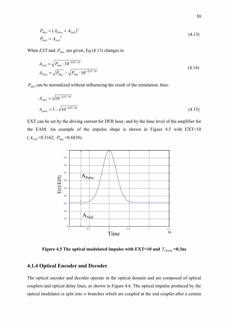
50
(4.13) 2
2)(
NullNull
NullPulseMax
AP
AAP
=
+=
When EXT and are given, Eq (4.13) changes to MaxP
10/
10/
10
10EXT
MaxMaxPulse
EXTMaxNull
PPA
PA−
−
⋅−=
⋅= (4.14)
MaxP can be normalized without influencing the result of the simulation, thus:
10/10 EXTNullA −=
10/101 EXTpulseA −−= (4.15)
EXT can be set by the driving current for DFB laser, and by the base level of the amplifier for
the EAM. An example of the impulse shape is shown in Figure 4.5 with EXT=10
( =0.3162, =0.6838). NullA MaxP
-1 -0.5 0 0.5 1 1.50
0.1
0.2
0.3
0.4
0.5
0.6
0.7
0.8
0.9
1
ns
E(t)/
E(0) APulse
ANull
Time
Figure 4.5 The optical modulated impulse with EXT=10 and T =0.3ns FWHM
4.1.4 Optical Encoder and Decoder
The optical encoder and decoder operate in the optical domain and are composed of optical
couplers and optical delay lines, as shown in Figure 4.6. The optical impulse produced by the
optical modulator is split into w branches which are coupled at the end coupler after a certain
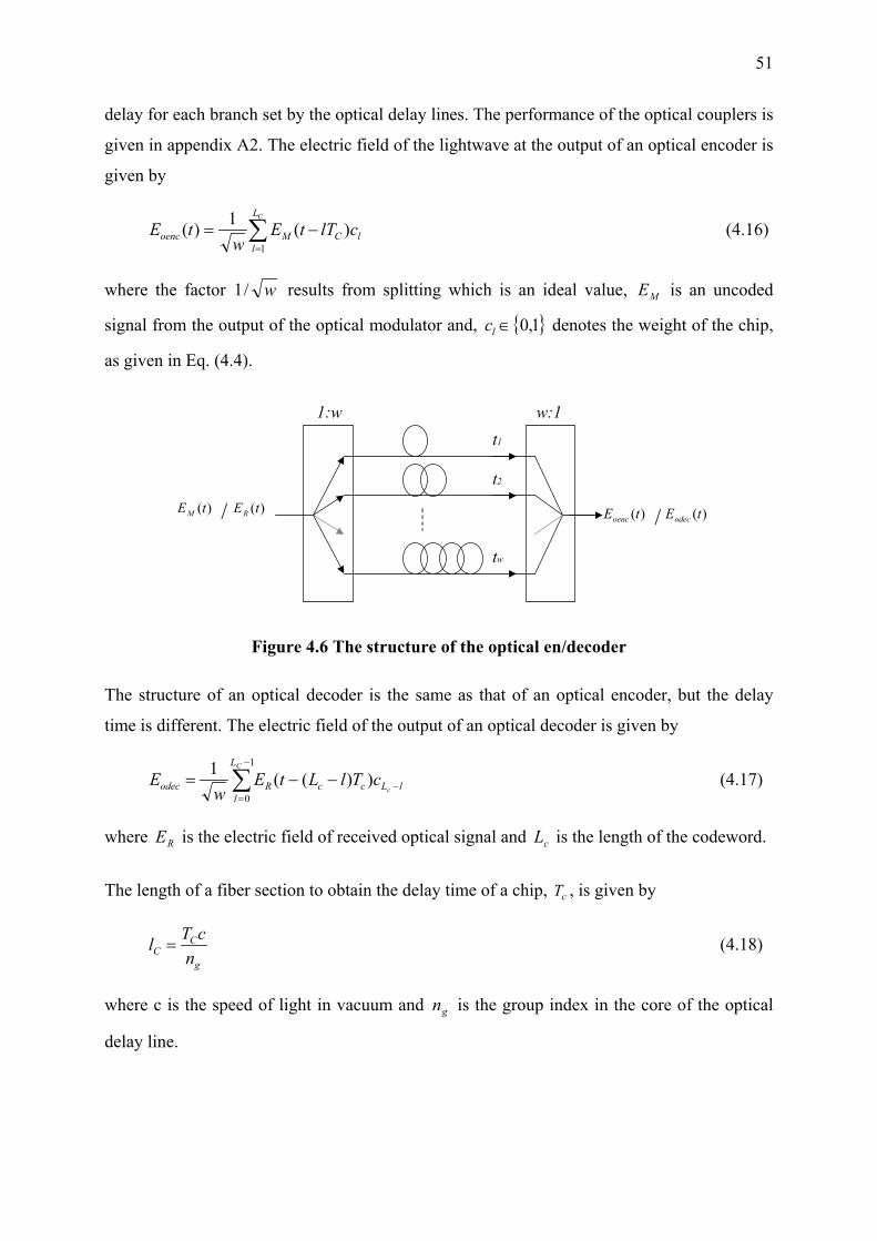
51
delay for each branch set by the optical delay lines. The performance of the optical couplers is
given in appendix A2. The electric field of the lightwave at the output of an optical encoder is
given by
∑=
−=CL
llCMoenc clTtE
wtE
1)(1)( (4.16)
where the factor w/1 results from splitting which is an ideal value, is an uncoded
signal from the output of the optical modulator and,
ME
1,0∈lc denotes the weight of the chip,
as given in Eq. (4.4).
t1
t2
tw
1:w w:1
)(tEM )(tEoenc )(tEodec)(tER/ /
Figure 4.6 The structure of the optical en/decoder
The structure of an optical decoder is the same as that of an optical encoder, but the delay
time is different. The electric field of the output of an optical decoder is given by
lLcc
L
lRodec c
C
cTlLtEw
E −
−
=
−−= ∑ ))((1 1
0(4.17)
where is the electric field of received optical signal and is the length of the codeword. RE cL
The length of a fiber section to obtain the delay time of a chip, T , is given by c
g
CC n
cTl = (4.18)
where c is the speed of light in vacuum and is the group index in the core of the optical
delay line.
gn
52
4.1.5 Optical Channel (Optical Fiber)
In a PON the optical channel is composed of optical fibers and optical couplers. Optical
couplers consume a great deal of optical power which must be considered in the calculation of
the optical power budget. For the system adopted in the present study, the optical couplers
have little nonlinear characteristics, therefore, the effect on S/N ratio from the optical couplers
will be ignored in the analysis. However, the influences caused by dispersion, PMD and other
linear impairments of the optical fiber on the quality of transmission will be considered.
The chromatic Dispersion: The propagation characteristics for each wavelength
depend on the refractive index of the fiber and on the nonlinearity of the propagation constant.
The optical chips are subject to impulse broadening as they propagate in the optical fiber. For
the single-mode fiber impulse broadening is solely caused by the so-called intramodal
dispersion. The dispersion parameter D is obtained by deriving the group-delay Tg with
respect to wavelength λ [77]:
WMg DD
ddT
LD +==
λ1 (4.19)
where
2
21λ
λλ d
ndcd
dnc
D gM −==
( ) ( )
−
⋅
∆= 2
22
dVVbdV
nn
dVVbd
ddn
cD gg
W λλ
in which ng is the group index, b is propagation constant, V is characteristic frequency and ∆
is the index difference of the core and the cladding. D has two components: one arising from
the material dispersion, DM, the other from the waveguide dispersion, DW. DW can be seen to
be proportional to the small parameter ∆. It is generally smaller than DM. DM crosses the λ–
axis near 1.3µm for the standard fiber. In this case, DW can be tailored through an
optimization of the waveguide profile and plays a crucial role in defining the exact location of
the overall zero dispersion wavelength.
PMD: Polarization-mode dispersion (PMD) is caused by asymmetries and stress
distribution in the fiber core, which locally leads to birefringence, i.e. a polarization-
dependent refractive index. It is another reason which influences the signals transmitted in the
optical fiber. In OCDMA system there are multiple lightwaves, that are emitted from different
53
lasers in local ONU. After transmission through the fiber, the lightwaves have different states
of polarization at the optical receiver. The optical signal to noise ratio decreases due to the
effect of the interference.
4.1.6 O/E Converter with Electronic Amplifiers
Unlike the normal on-off keying, in optical communication systems with OCDMA the main
noise comes from interference by other users. The performance is not sensitive to the noise of
the O/E converter and pre-amplifiers at receiver. So, they can be ignored here, and the O/E
converter can be assumed as ideal. The output of an optical receiver including O/E converter
and amplifiers is given by
2/ )()()( tEtfAtU REO ⋅⋅⋅= η (4.20)
where η is the efficiency of opto-electronic conversion, A is the amplification coefficient,
both of which can be normalized to 1 without affecting the value of S/N. is electrical
field strength of the received optical signal. is the impulse response of the equalizer
filter of the optical receiver and amplifiers, which can be expressed by the fifth-order Bessel
filter. The Laplace transform F(s) is given by [60]
)(tER
)(tf
94594542010515945)( 2345 +++++
=sssss
sF (4.21)
4.1.7 Electronic Decoder
The electronic decoder is composed of electronic delay lines (coaxial cable), the signal splitter
and signal coupler. There are two types of the signal couplers: additive coupler and logic
AND coupler. The electronic decoder with additive coupler has a same function as an optical
decoder. The electronic decoder with logic coupler is composed of logic circuits. Firstly, the
signal is digitized by a decision at the input of the decoder, then the binary signal is split into
w branches which are then coupled into coaxial cable delay lines. After transmission through
the coaxial cables with different delay times suited for the codeword, the signals will be
processed by AND logic. This processing can be express as
( )( )[ ]∏−
=−−−=
1
0/
C
C
L
llLCCEOedec cTlLtUgE (4.22)
where Π denote multiply and is the decision function, given by [ ]xg
54
≤≤>
=θ
θx
xxg
0,0,1
][ (4.23)
An additional advantage of this decoder is that it has the function of a hard-limiter for the
undecoded signal, hence the BER can be reduced without further operation.
4.2 Interferometric Noise
OCDMA system is an interference-limited-system. Though the interferometric noise has
attracted much attentions in the areas of WDM and OTDM networks [78, 79, 69], only
several papers can be found concerning OCDMA system. Tancevski and Rusch [80] analyzed
impact of the beat noise on the performance of 2-D OCDMA system, focus was on the impact
between different frequency points. The analysis of the influence of optical noise on
OCDMA, especially for narrow band optical source was rarely addressed up to now.
4.2.1 Characteristics of Interferometric Noise
The electric field of a CW optical source can be given as
)))((exp()( 00 ttjEtE φω += (4.24)
where 0ω is the optical frequency, )(tφ is the phase noise which is a random time varying
component resulting from spontaneous emission events [64]. Considering the addition of two
CWs and their crosstalk, the interferometric noise may be classified as follows [65]:
Case a) If the two CWs are from the same source and suffer a differential delay τ between
source and detector, their relative phase arrived at the detector is
),()()()(
0
0
ττωτφφτωφ
tttt
Φ+=−−+=∆
(4.25)
The coherence time, cτ , of the laser source provides the characterization of phase
fluctuations. For the 1550nm band DFB laser, cτ ranges from several nanoseconds to a few
100ns. ( )τ,tΦ has a close relationship with cτ when τ is fixed. For a chirp free impulse
source, ( )τ,tΦ can be approximated as a zero-mean Gaussian process of Wiener form [78].
Coherent Crosstalk: τ is much smaller than cτ , resulting in an interference very close to the
coherence limit ( 0=τ ), which is characterized by an absence of laser phase noise (variance
55
of ),( τtΦ <<2π ). However, significant interferometric noise may arise from slow fluctuations
in τ induced by temperature fluctuations and phonon excitations in optical fiber-
environmental phase noise. If τ is constant, the interferometric noise is static and may be
determined.
(exp(0 j φ+ exp(
[ )(t(φ∆ ω
Incoherent Beat Noise Crosstalk (also called phase induced intensity noise, PIIN): τ is
much greater than cτ , resulting in an interference at the so-called “incoherent limit” [65],
such that the variance ),( τtΦ >>2π . Here the interferometric noise is driven by the laser
phase noise which masks any influence of the (lower bandwidth) environmental phase noise.
Partially Coherent Crosstalk: this class falls between the two extremes of coherent and
incoherent beat noise crosstalk.
Case b) Crosstalk arise from distinct laser sources, their electric fields are given as
)))(ttE ddω and )))((0 ttjE xx φω + . The relative phase is given as
( ) ])() ttt xdxd φφω −+−= (4.26)
Incoherent Noise-Free Crosstalk: if the beat frequency of the two laser, πωω 2/)( xd − ,
exceeds the receiver bandwidth, then the interferometric noise is removed by electrical
filtering following detection, and only additive crosstalk components remain.
Incoherent Beat Noise Crosstalk: if the beat frequency of the two lasers, πωω 2/)( xd −
txd )(
, is
smaller than the receiver bandwidth, then the cyclic variation in phase due to ωω − , and
the random variation due to the phase noise elements, generate interferometric noise. This is
also called incoherent beat noise crosstalk because the mixing is incoherent.
The case a) would occur at the optical en/decoder: at optical encoder partially coherent
crosstalk occurs and at optical decoder coherent crosstalk occurs. And case b) would occur
due to the interference by other OCDMA channels with different optical sources. The
intensity of the interferometric noise mainly depends on the phase noise of optical source and
phase noise introduced by environment.
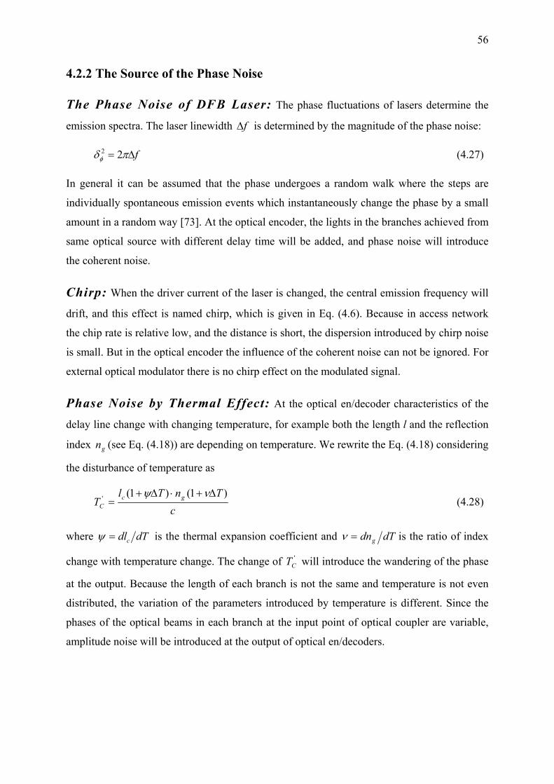
56
4.2.2 The Source of the Phase Noise
The Phase Noise of DFB Laser: The phase fluctuations of lasers determine the
emission spectra. The laser linewidth f∆ is determined by the magnitude of the phase noise:
f∆= πδφ 22 (4.27)
In general it can be assumed that the phase undergoes a random walk where the steps are
individually spontaneous emission events which instantaneously change the phase by a small
amount in a random way [73]. At the optical encoder, the lights in the branches achieved from
same optical source with different delay time will be added, and phase noise will introduce
the coherent noise.
Chirp: When the driver current of the laser is changed, the central emission frequency will
drift, and this effect is named chirp, which is given in Eq. (4.6). Because in access network
the chip rate is relative low, and the distance is short, the dispersion introduced by chirp noise
is small. But in the optical encoder the influence of the coherent noise can not be ignored. For
external optical modulator there is no chirp effect on the modulated signal.
Phase Noise by Thermal Effect: At the optical en/decoder characteristics of the
delay line change with changing temperature, for example both the length l and the reflection
index (see Eq. (4.18)) are depending on temperature. We rewrite the Eq. (4.18) considering
the disturbance of temperature as
gn
cTnTl
T gcC
)1()1(' ∆+⋅∆+=
νψ (4.28)
where dTdlc=ψ is the thermal expansion coefficient and dTdng=ν is the ratio of index
change with temperature change. The change of T will introduce the wandering of the phase
at the output. Because the length of each branch is not the same and temperature is not even
distributed, the variation of the parameters introduced by temperature is different. Since the
phases of the optical beams in each branch at the input point of optical coupler are variable,
amplitude noise will be introduced at the output of optical en/decoders.
'C
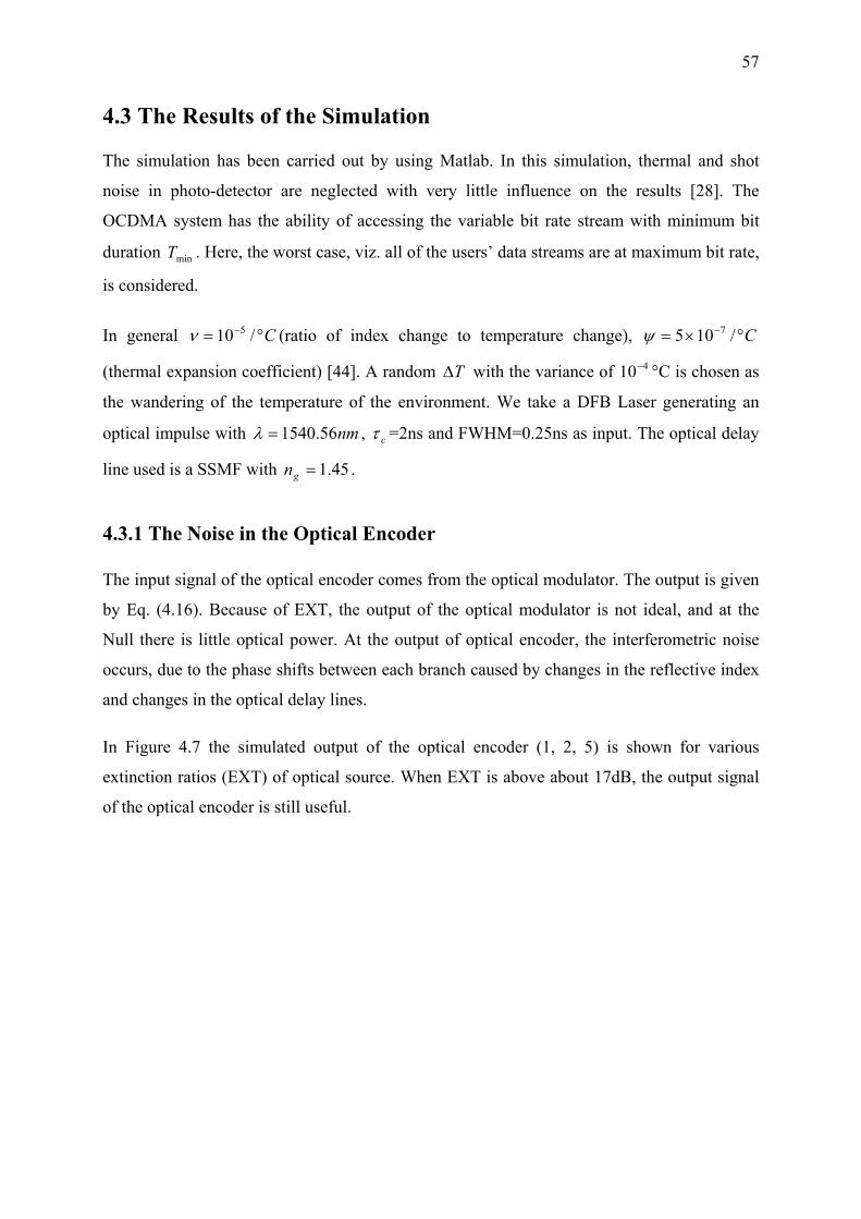
57
4.3 The Results of the Simulation
The simulation has been carried out by using Matlab. In this simulation, thermal and shot
noise in photo-detector are neglected with very little influence on the results [28]. The
OCDMA system has the ability of accessing the variable bit rate stream with minimum bit
duration T . Here, the worst case, viz. all of the users’ data streams are at maximum bit rate,
is considered.
min
In general (ratio of index change to temperature change),
(thermal expansion coefficient) [44]. A random
C°= − /10 5ν C°×= − /105 7ψ
T∆ with the variance of 10 °C is chosen as
the wandering of the temperature of the environment. We take a DFB Laser generating an
optical impulse with
4−
nm56.1540=λ , cτ =2ns and FWHM=0.25ns as input. The optical delay
line used is a SSMF with . 45.1=gn
4.3.1 The Noise in the Optical Encoder
The input signal of the optical encoder comes from the optical modulator. The output is given
by Eq. (4.16). Because of EXT, the output of the optical modulator is not ideal, and at the
Null there is little optical power. At the output of optical encoder, the interferometric noise
occurs, due to the phase shifts between each branch caused by changes in the reflective index
and changes in the optical delay lines.
In Figure 4.7 the simulated output of the optical encoder (1, 2, 5) is shown for various
extinction ratios (EXT) of optical source. When EXT is above about 17dB, the output signal
of the optical encoder is still useful.
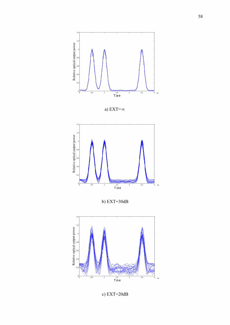
58
0 0.5 1 1.5 2 2.5 30
0.2
0.4
0.6
0.8
1
1.2
1.4
the output of the optical encoder by EXT=unlimited
the
optic
al p
ower
ns
Time
Rel
ativ
e op
tical
out
put p
ower
a) EXT= ∞
0 0.5 1 1.5 2 2.5 30
0.2
0.4
0.6
0.8
1
1.2
1.4
The
opt
ical
pow
er
the output of the encoder by EXT=30ns
Time
Rel
ativ
e op
tical
out
put p
ower
b) EXT=30dB
0 0.5 1 1.5 2 2.5 30
0.2
0.4
0.6
0.8
1
1.2
1.4
The
opt
ical
pow
er
the output of the encoder by EXT=20ns
Time
Rel
ativ
e op
tical
out
put p
ower
c) EXT=20dB
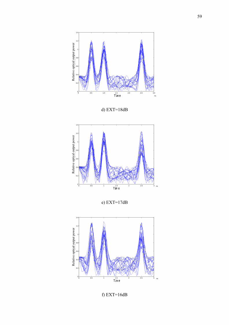
59
0 0.5 1.0 1.5 2.0 2.5 3.00
0.2
0.4
0.6
0.8
1
1.2
1.4
The
opt
ical
pow
er
the output of the encoder by EXT=18 ns Time
Rel
ativ
e op
tical
out
put p
ower
d) EXT=18dB
0 0.5 1 1.5 2 2.5 30
0.2
0.4
0.6
0.8
1
1.2
1.4
The
opt
ical
pow
er
the output of the encoder by EXT=17ns
Time
Rel
ativ
e op
tical
out
put p
ower
e) EXT=17dB
0 0.5 1 1.5 2 2.5 30
0.2
0.4
0.6
0.8
1
1.2
1.4
The
opt
ical
pow
er
the output of the encoder by EXT=16ns
Time
Rel
ativ
e op
tical
out
put p
ower
f) EXT=16dB
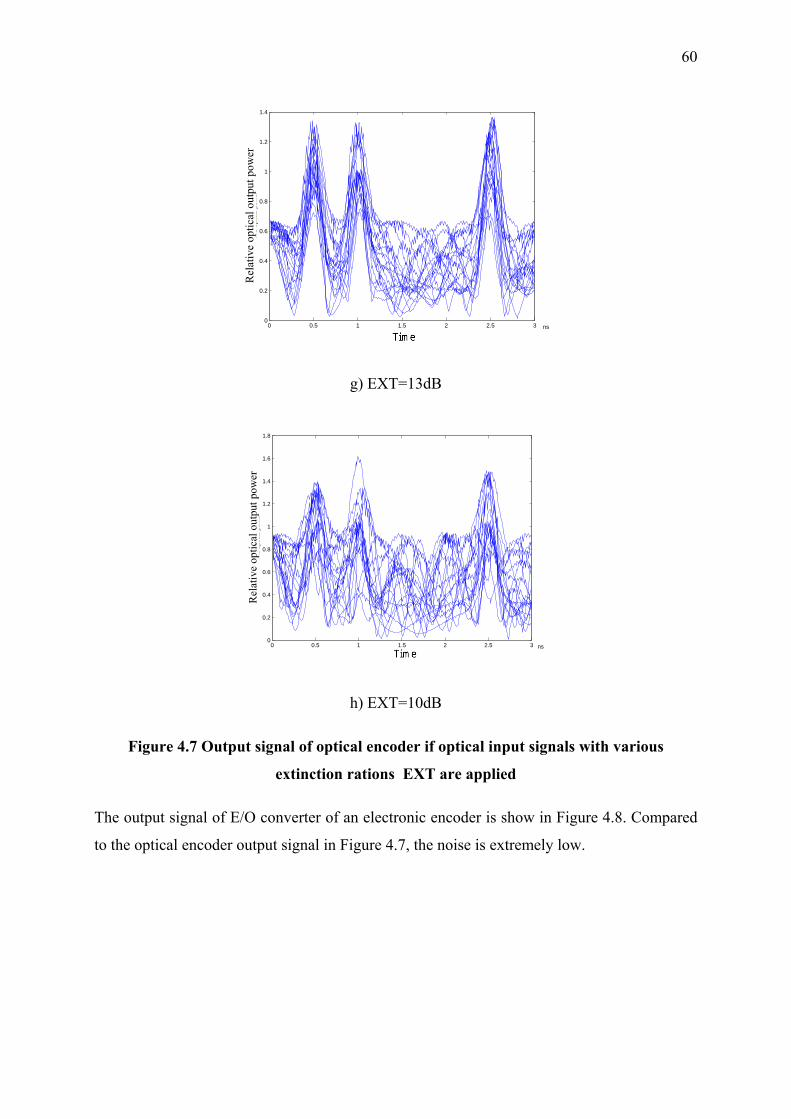
60
0 0.5 1 1.5 2 2.5 30
0.2
0.4
0.6
0.8
1
1.2
1.4
The
opt
ical
pow
er
the output of the encoder by EXT=13ns
Time
Rel
ativ
e op
tical
out
put p
ower
g) EXT=13dB
0 0.5 1 1.5 2 2.5 30
0.2
0.4
0.6
0.8
1
1.2
1.4
1.6
1.8
The
opt
ical
pow
er
the output of the encoder by EXT=10ns
Time
Rel
ativ
e op
tical
out
put p
ower
h) EXT=10dB
Figure 4.7 Output signal of optical encoder if optical input signals with various
extinction rations EXT are applied
The output signal of E/O converter of an electronic encoder is show in Figure 4.8. Compared
to the optical encoder output signal in Figure 4.7, the noise is extremely low.
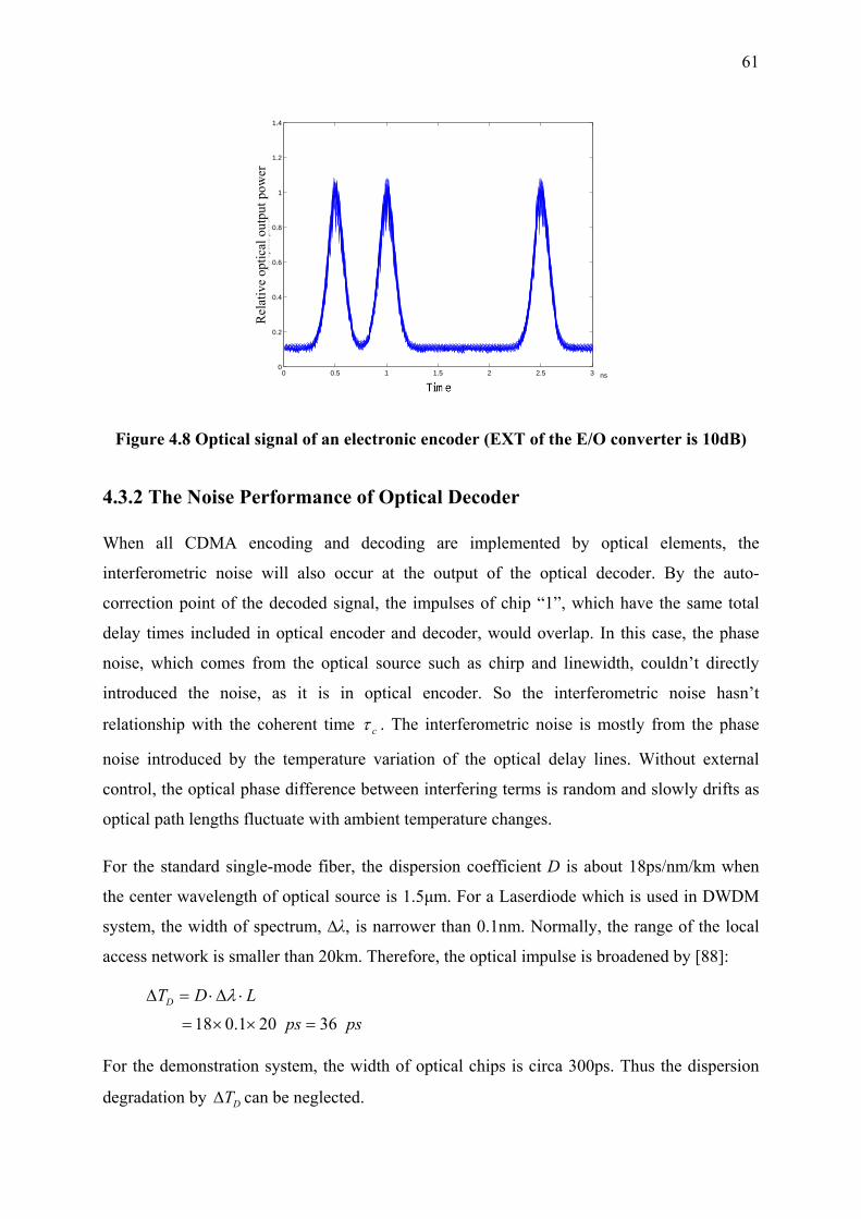
61
0 0.5 1 1.5 2 2.5 30
0.2
0.4
0.6
0.8
1
1.2
1.4
The
opt
ical
pow
er
the output of electronic encoder by EXT=10ns
Time
Rel
ativ
e op
tical
out
put p
ower
Figure 4.8 Optical signal of an electronic encoder (EXT of the E/O converter is 10dB)
4.3.2 The Noise Performance of Optical Decoder
When all CDMA encoding and decoding are implemented by optical elements, the
interferometric noise will also occur at the output of the optical decoder. By the auto-
correction point of the decoded signal, the impulses of chip “1”, which have the same total
delay times included in optical encoder and decoder, would overlap. In this case, the phase
noise, which comes from the optical source such as chirp and linewidth, couldn’t directly
introduced the noise, as it is in optical encoder. So the interferometric noise hasn’t
relationship with the coherent time cτ . The interferometric noise is mostly from the phase
noise introduced by the temperature variation of the optical delay lines. Without external
control, the optical phase difference between interfering terms is random and slowly drifts as
optical path lengths fluctuate with ambient temperature changes.
For the standard single-mode fiber, the dispersion coefficient D is about 18ps/nm/km when
the center wavelength of optical source is 1.5µm. For a Laserdiode which is used in DWDM
system, the width of spectrum, ∆λ, is narrower than 0.1nm. Normally, the range of the local
access network is smaller than 20km. Therefore, the optical impulse is broadened by [88]:
psps
LDTD
36201.018 =××=
⋅∆⋅=∆ λ
For the demonstration system, the width of optical chips is circa 300ps. Thus the dispersion
degradation by can be neglected.DT∆
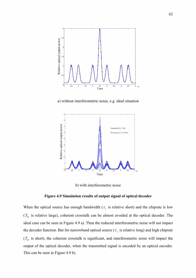
62
0 0.5 1 1.5 2 2.5 3 3.5 4 4.5 50
0.5
1
1.5
2
2.5
3
The
opt
ical
pow
er
the ideal output of the optical encoderns
Time
Rel
ativ
e op
tical
out
put p
ower
a) without interferometric noise, e.g. ideal situation
Time
Rel
ativ
e op
tical
out
put p
ower
b) with interferometric noise
Figure 4.9 Simulation results of output signal of optical decoder
When the optical source has enough bandwidth ( cτ is relative short) and the chiprate is low
( is relative large), coherent crosstalk can be almost avoided at the optical decoder. The
ideal case can be seen in Figure 4.9 a). Then the reduced interferometric noise will not impact
the decoder function. But for narrowband optical source (
DT
cτ is relative long) and high chiprate
( is short), the coherent crosstalk is significant, and interferometric noise will impact the
output of the optical decoder, when the transmitted signal is encoded by an optical encoder.
This can be seen in Figure 4.9 b).
DT
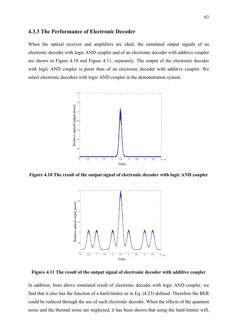
63
4.3.3 The Performance of Electronic Decoder
When the optical receiver and amplifiers are ideal, the simulated output signals of an
electronic decoder with logic AND coupler and of an electronic decoder with additive coupler
are shown in Figure 4.10 and Figure 4.11, separately. The output of the electronic decoder
with logic AND coupler is purer than of an electronic decoder with additive coupler. We
select electronic decoders with logic AND coupler in the demonstration system.
Time
Rel
ativ
e op
tical
out
put p
ower
Figure 4.10 The result of the output signal of electronic decoder with logic AND coupler
Time
Rel
ativ
e op
tical
out
put p
ower
Figure 4.11 The result of the output signal of electronic decoder with additive coupler
In addition, from above simulated result of electronic decoder with logic AND coupler, we
find that it also has the function of a hard-limiter as in Eq. (4.23) defined. Therefore the BER
could be reduced through the use of such electronic decoder. When the effects of the quantum
noise and the thermal noise are neglected, it has been shown that using the hard-limiter will,
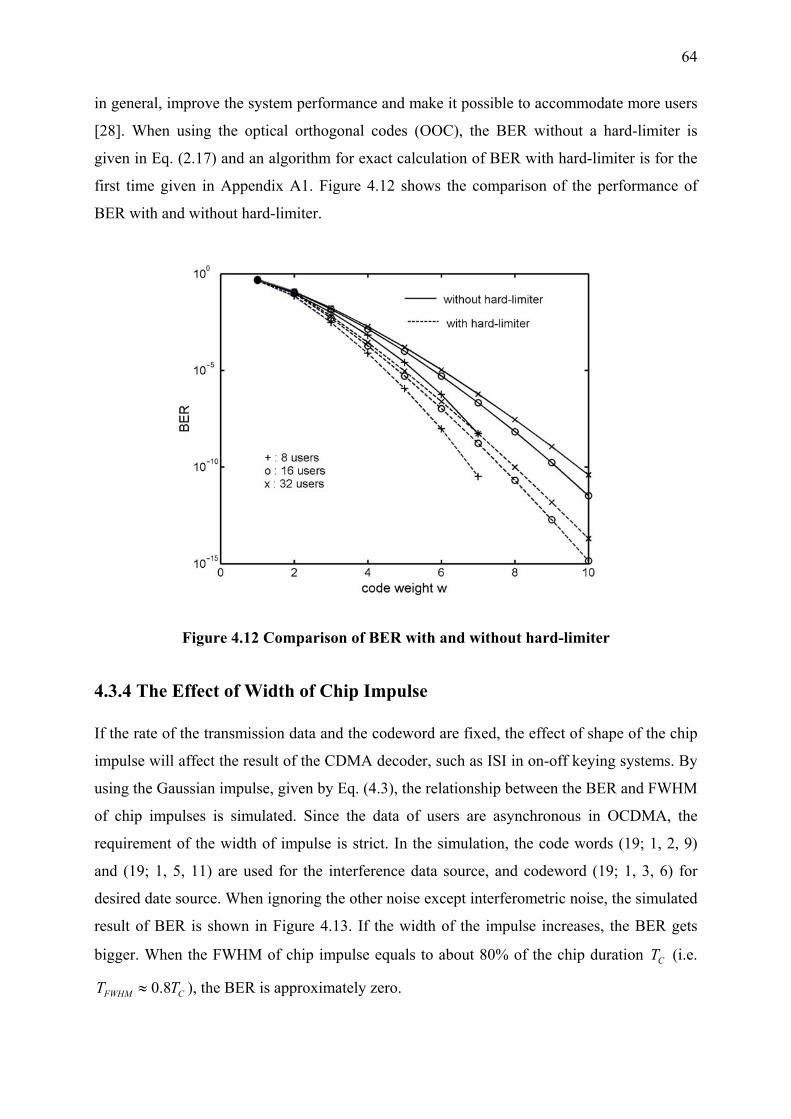
64
in general, improve the system performance and make it possible to accommodate more users
[28]. When using the optical orthogonal codes (OOC), the BER without a hard-limiter is
given in Eq. (2.17) and an algorithm for exact calculation of BER with hard-limiter is for the
first time given in Appendix A1. Figure 4.12 shows the comparison of the performance of
BER with and without hard-limiter.
Figure 4.12 Comparison of BER with and without hard-limiter
4.3.4 The Effect of Width of Chip Impulse
If the rate of the transmission data and the codeword are fixed, the effect of shape of the chip
impulse will affect the result of the CDMA decoder, such as ISI in on-off keying systems. By
using the Gaussian impulse, given by Eq. (4.3), the relationship between the BER and FWHM
of chip impulses is simulated. Since the data of users are asynchronous in OCDMA, the
requirement of the width of impulse is strict. In the simulation, the code words (19; 1, 2, 9)
and (19; 1, 5, 11) are used for the interference data source, and codeword (19; 1, 3, 6) for
desired date source. When ignoring the other noise except interferometric noise, the simulated
result of BER is shown in Figure 4.13. If the width of the impulse increases, the BER gets
bigger. When the FWHM of chip impulse equals to about 80% of the chip duration T (i.e.
), the BER is approximately zero.
C
CFWHM TT 8.0≈
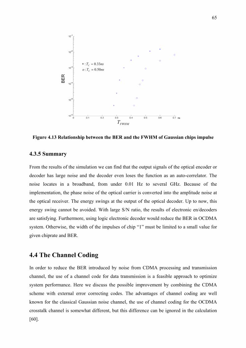
65
BER
nsTonsT
C
C
50.0:33.0:
==∗
FWHMT
Figure 4.13 Relationship between the BER and the FWHM of Gaussian chips impulse
4.3.5 Summary
From the results of the simulation we can find that the output signals of the optical encoder or
decoder has large noise and the decoder even loses the function as an auto-correlator. The
noise locates in a broadband, from under 0.01 Hz to several GHz. Because of the
implementation, the phase noise of the optical carrier is converted into the amplitude noise at
the optical receiver. The energy swings at the output of the optical decoder. Up to now, this
energy swing cannot be avoided. With large S/N ratio, the results of electronic en/decoders
are satisfying. Furthermore, using logic electronic decoder would reduce the BER in OCDMA
system. Otherwise, the width of the impulses of chip “1” must be limited to a small value for
given chiprate and BER.
4.4 The Channel Coding
In order to reduce the BER introduced by noise from CDMA processing and transmission
channel, the use of a channel code for data transmission is a feasible approach to optimize
system performance. Here we discuss the possible improvement by combining the CDMA
scheme with external error correcting codes. The advantages of channel coding are well
known for the classical Gaussian noise channel, the use of channel coding for the OCDMA
crosstalk channel is somewhat different, but this difference can be ignored in the calculation
[60].
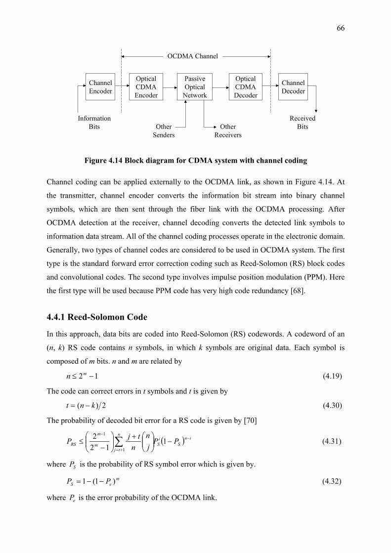
66
PassiveOptical
Network
ChannelEncoder
OpticalCDMAEncoder
OpticalCDMADecoder
ChannelDecoder
OCDMA Channel
InformationBits
ReceivedBitsOther
SendersOther
Receivers
Figure 4.14 Block diagram for CDMA system with channel coding
Channel coding can be applied externally to the OCDMA link, as shown in Figure 4.14. At
the transmitter, channel encoder converts the information bit stream into binary channel
symbols, which are then sent through the fiber link with the OCDMA processing. After
OCDMA detection at the receiver, channel decoding converts the detected link symbols to
information data stream. All of the channel coding processes operate in the electronic domain.
Generally, two types of channel codes are considered to be used in OCDMA system. The first
type is the standard forward error correction coding such as Reed-Solomon (RS) block codes
and convolutional codes. The second type involves impulse position modulation (PPM). Here
the first type will be used because PPM code has very high code redundancy [68].
4.4.1 Reed-Solomon Code
In this approach, data bits are coded into Reed-Solomon (RS) codewords. A codeword of an
(n, k) RS code contains n symbols, in which k symbols are original data. Each symbol is
composed of m bits. n and m are related by
12 −≤ mn (4.19)
The code can correct errors in t symbols and t is given by
2)( knt −= (4.30)
The probability of decoded bit error for a RS code is given by [70]
( ) inS
iS
n
tjm
m
RS PPjn
ntjP −
+=
−
−
+
−
≤ ∑ 112
21
1
(4.31)
where is the probability of RS symbol error which is given by. SP
meS PP )1(1 −−= (4.32)
where is the error probability of the OCDMA link. eP
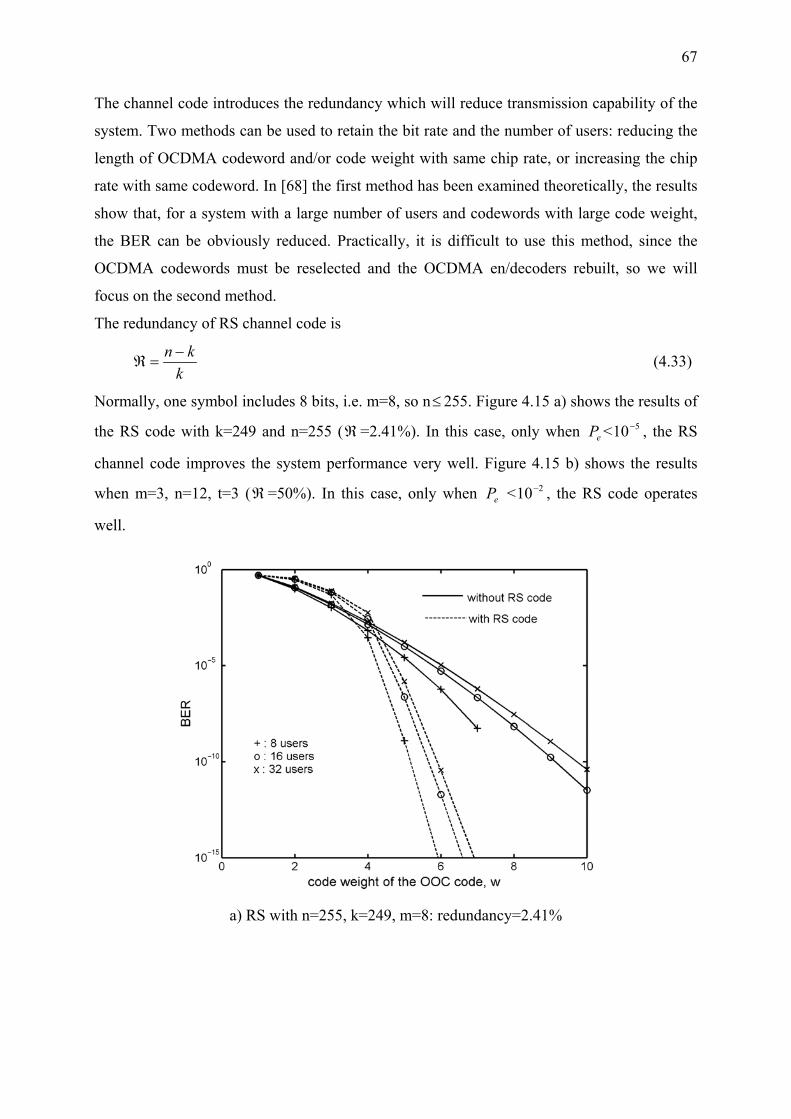
67
The channel code introduces the redundancy which will reduce transmission capability of the
system. Two methods can be used to retain the bit rate and the number of users: reducing the
length of OCDMA codeword and/or code weight with same chip rate, or increasing the chip
rate with same codeword. In [68] the first method has been examined theoretically, the results
show that, for a system with a large number of users and codewords with large code weight,
the BER can be obviously reduced. Practically, it is difficult to use this method, since the
OCDMA codewords must be reselected and the OCDMA en/decoders rebuilt, so we will
focus on the second method.
The redundancy of RS channel code is
kkn −
=ℜ (4.33)
Normally, one symbol includes 8 bits, i.e. m=8, so n ≤ 255. Figure 4.15 a) shows the results of
the RS code with k=249 and n=255 (ℜ =2.41%). In this case, only when <10 , the RS
channel code improves the system performance very well. Figure 4.15 b) shows the results
when m=3, n=12, t=3 (ℜ =50%). In this case, only when <10 , the RS code operates
well.
eP 5−
eP 2−
a) RS with n=255, k=249, m=8: redundancy=2.41%
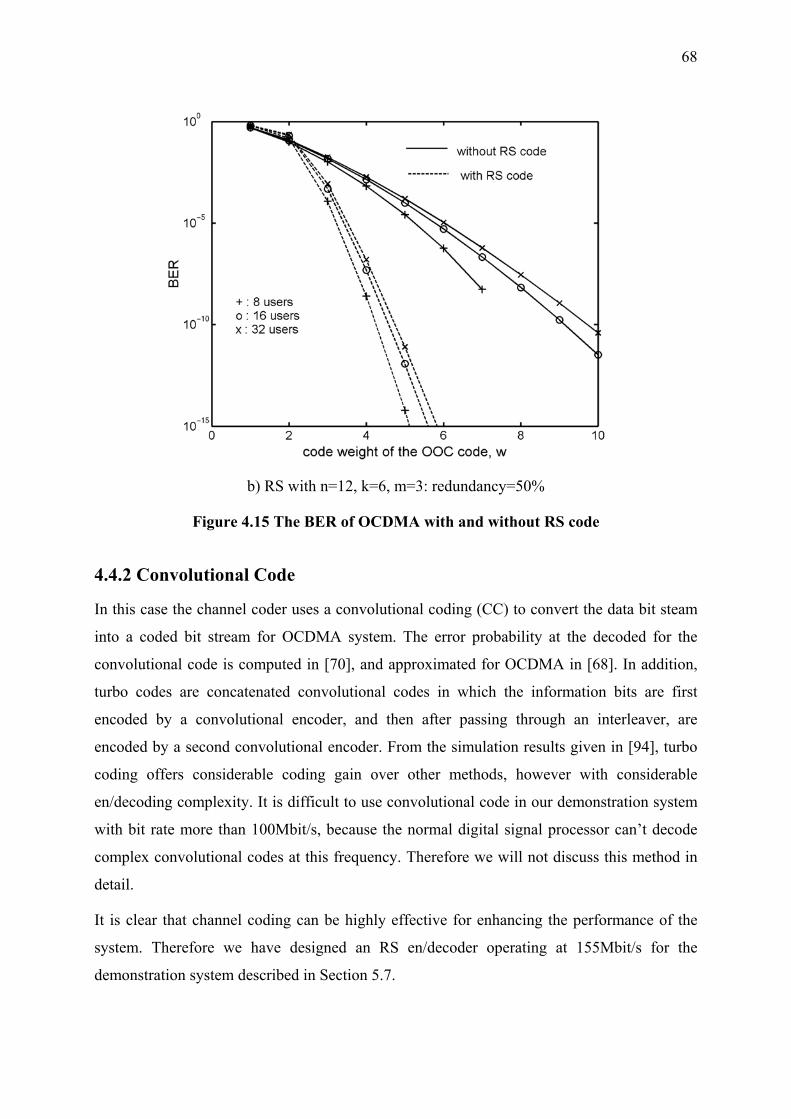
68
b) RS with n=12, k=6, m=3: redundancy=50%
Figure 4.15 The BER of OCDMA with and without RS code
4.4.2 Convolutional Code
In this case the channel coder uses a convolutional coding (CC) to convert the data bit steam
into a coded bit stream for OCDMA system. The error probability at the decoded for the
convolutional code is computed in [70], and approximated for OCDMA in [68]. In addition,
turbo codes are concatenated convolutional codes in which the information bits are first
encoded by a convolutional encoder, and then after passing through an interleaver, are
encoded by a second convolutional encoder. From the simulation results given in [94], turbo
coding offers considerable coding gain over other methods, however with considerable
en/decoding complexity. It is difficult to use convolutional code in our demonstration system
with bit rate more than 100Mbit/s, because the normal digital signal processor can’t decode
complex convolutional codes at this frequency. Therefore we will not discuss this method in
detail.
It is clear that channel coding can be highly effective for enhancing the performance of the
system. Therefore we have designed an RS en/decoder operating at 155Mbit/s for the
demonstration system described in Section 5.7.
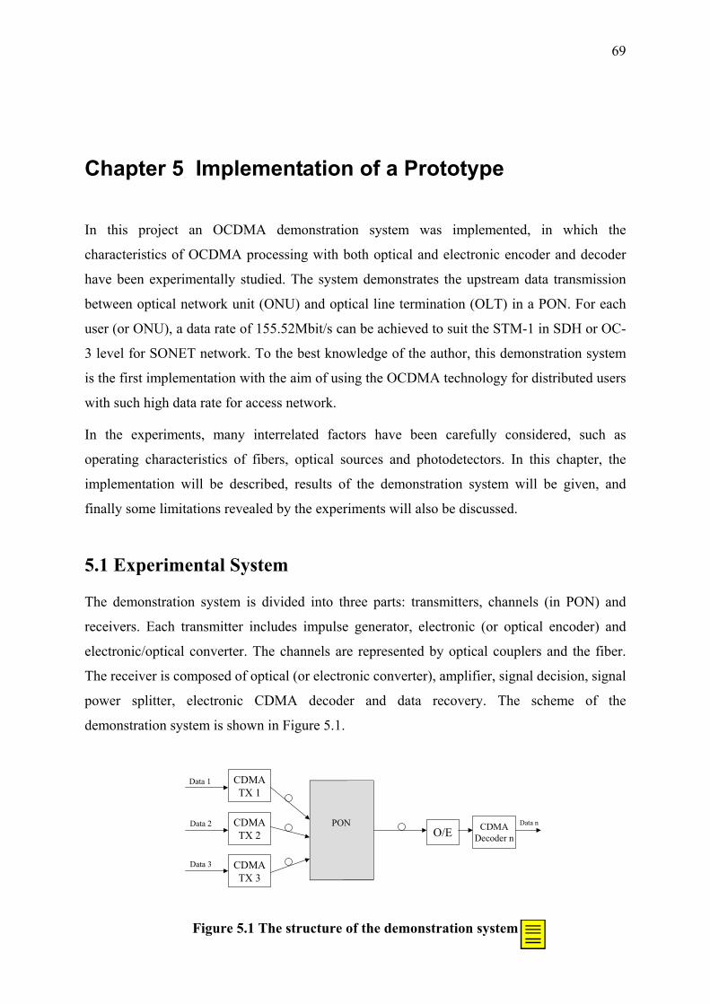
69
Chapter 5 Implementation of a Prototype
In this project an OCDMA demonstration system was implemented, in which the
characteristics of OCDMA processing with both optical and electronic encoder and decoder
have been experimentally studied. The system demonstrates the upstream data transmission
between optical network unit (ONU) and optical line termination (OLT) in a PON. For each
user (or ONU), a data rate of 155.52Mbit/s can be achieved to suit the STM-1 in SDH or OC-
3 level for SONET network. To the best knowledge of the author, this demonstration system
is the first implementation with the aim of using the OCDMA technology for distributed users
with such high data rate for access network.
In the experiments, many interrelated factors have been carefully considered, such as
operating characteristics of fibers, optical sources and photodetectors. In this chapter, the
implementation will be described, results of the demonstration system will be given, and
finally some limitations revealed by the experiments will also be discussed.
5.1 Experimental System
The demonstration system is divided into three parts: transmitters, channels (in PON) and
receivers. Each transmitter includes impulse generator, electronic (or optical encoder) and
electronic/optical converter. The channels are represented by optical couplers and the fiber.
The receiver is composed of optical (or electronic converter), amplifier, signal decision, signal
power splitter, electronic CDMA decoder and data recovery. The scheme of the
demonstration system is shown in Figure 5.1.
CDMATX 1
CDMATX 2
CDMATX 3
CDMADecoder n
Data 1
Data 2
Data 3
O/EData nPON
Figure 5.1 The structure of the demonstration system
yjzhang
These coding scheme is used to introduce randomness (and redundancy) into the digital information stream to ensure efficient timing recovery (and to facilitate error monitoring) at the receiver.
70
Bit Rate: For upstream links in the access network, the transmission bit rate in the near
future is estimated to be in the level of STM-1. Based on this, components operating at the
frequency corresponding to a data rate of 2.5Gbit/s were chosen. In practice, the chip rate can
be up to 3.0Gchip/s and each of three accessed data rates can be up to 160Mbit/s.
Wavelength: The OCDMA system can actually operate at any wavelength. However, here
the 1550nm band was chosen, in order to easily combine with DWDM technology in future,
which is developed very well in this band [88]. To avoid the incoherent beat noise crosstalk
introduced in section 4.2, the wavelength of each Laserdiode is not exactly the same.
Power Budget of the optical Link: The optical power budget is an important
factor for the design of the optical system. Nowadays, some kinds of Laserdiodes for optical
communication can launch a peak power up to +20dBm, but normally it isn’t used at the
extreme case considering its life time. Here the output power was set at +10dBm (denotes as
=10dBm). Each optical encoder or decoder with four taps (code weight less than 5)
consumes 12dB optical power as a minimum, in which 6dB is consumed by 1:4 optical
splitter and the other 6dB by 4:1 optical coupler (in principle, 4:1 optical couplers could be
constructed with 0dB optical loss, but here they are implemented with normal optical
couplers). If 1dB is taken as the extra loss in practice, then the losses of optical power in
optical encoder and decoder are =13dB and =13dB, respectively (electronic
en/decoders don’t consume optical power). The PON network is represented by a 4:1 optical
coupler which also needs 6dB in principle. Here =6.5dB is taken in practice. When there
are 10 km standard optical fiber used for the transmission link between the transmitter and the
receiver in access network, the loss of the optical fiber is only 2dB. Considering the loss of
the moveable connectors, we take 4dB for the whole optical link, i.e. =4dB. For optical
receiver, in ITU standard the sensitivity of 2.5Gbit/s optical transmission system can be
smaller than –27dBm. Here our optical receiver has a signal to noise ratio high enough to
reach this standard, thus here the sensitivity of the optical receiver is chosen 27dBm in
system design.
LDP
enP deP
PONP
chP
RP
In this system, we demonstrate all combinations of the optical and electronic en/decoder.
When both optical encoder and optical decoder are used in an OCDMA channel, the optical
margin is
71
dBPPPPPPP RdeenchPONLDm
5.0=−−−−−=
(5.1)
When optical encoder and electronic decoder are used, or electronic encoder and optical
decoder are used in an OCDMA channel, the optical margin is
dBPPorPPPPP RdeenchPONLDm
5.13)(
=−−−−=
(5.2)
For OCDMA channel, in which electronic encoder and decoder are used, the optical margin is
dBPPPPP RchPONLDm
5.26=−−−=
(5.3)
At all cases, the optical power budget is enough, hence no optical EDFA needs to be used in
this demonstration system. However in a practical access network, the number of branches of
PON is large, the optical power loss would also be large, therefore, the use of EDFA is
necessary. At the optical receiver we adjust the optical power of transmitters with different
encoding process at the same level by using the variable optical attenuators, in order to
balance the interferometric noise for each OCDMA channel.
The Interface: The interface in this system operates with standard ECL level. Here we
do not build the clock recovery and data reshaper at the signal input, so the data sources have
to offer the clock. But it has no effect on the demonstration of OCDMA processing. The
system can access the data stream with variable bit rate lower than 250Mbit/s.
Some Improving of the System: In this demonstration system several new methods
will be employed in the implementation. Firstly, it is noticed that all of the receivers are at the
same location (at optical line termination), when the electronic decoders are used instead of
the optical decoder in conventional OCDMA system. Thus, the users can share the same
signal from a single O/E converter. In the final scheme, electronic decoders will be located
behind the O/E converter. Secondly, the signal from the electrical amplifier will be decided
between Mark and Null, then the electronic decoders will operate in logic domain instead of
analog domain. This will reduce the bit error rate and simplify the implementation. At last, the
electronic and optical delay line will be employed in the implementation of encoder, decoder
and impulse generator, which has benefit of simplifying the circuit design, as can be seen in
the following sections.
Is summary, the system is realized under the following rules:
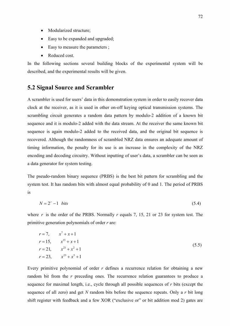
72
• Modularized structure;
• Easy to be expanded and upgraded;
• Easy to measure the parameters ;
• Reduced cost.
In the following sections several building blocks of the experimental system will be
described, and the experimental results will be given.
5.2 Signal Source and Scrambler
A scrambler is used for users’ data in this demonstration system in order to easily recover data
clock at the receiver, as it is used in other on-off keying optical transmission systems. The
scrambling circuit generates a random data pattern by modulo-2 addition of a known bit
sequence and it is modulo-2 added with the data stream. At the receiver the same known bit
sequence is again modulo-2 added to the received data, and the original bit sequence is
recovered. Although the randomness of scrambled NRZ data ensures an adequate amount of
timing information, the penalty for its use is an increase in the complexity of the NRZ
encoding and decoding circuitry. Without inputting of user’s data, a scrambler can be seen as
a data generator for system testing.
The pseudo-random binary sequence (PRBS) is the best bit pattern for scrambling and the
system test. It has random bits with almost equal probability of 0 and 1. The period of PRBS
is
bitsN r 12 −= (5.4)
where r is the order of the PRBS. Normally r equals 7, 15, 21 or 23 for system test. The
primitive generation polynomials of order r are:
1,231,21
1,151,7
523
221
15
7
++=
++=
++=
++=
xxrxxrxxr
xxr
(5.5)
Every primitive polynomial of order r defines a recurrence relation for obtaining a new
random bit from the r preceding ones. The recurrence relation guarantees to produce a
sequence for maximal length, i.e., cycle through all possible sequences of r bits (except the
sequence of all zero) and get N random bits before the sequence repeats. Only a r bit long
shift register with feedback and a few XOR (“exclusive or” or bit addition mod 2) gates are
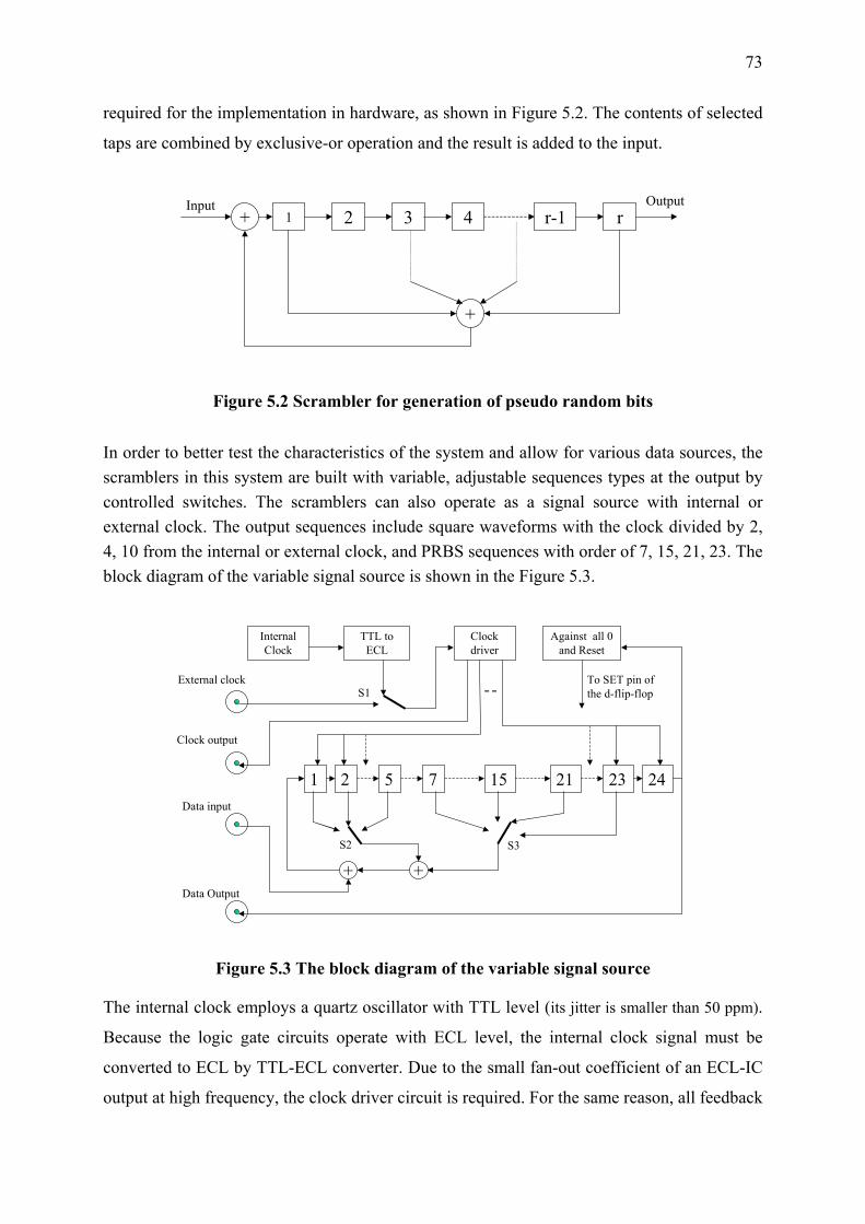
73
required for the implementation in hardware, as shown in Figure 5.2. The contents of selected
taps are combined by exclusive-or operation and the result is added to the input.
1 2 3 4 r-1 r
+
Output+
Input
Figure 5.2 Scrambler for generation of pseudo random bits
In order to better test the characteristics of the system and allow for various data sources, the scramblers in this system are built with variable, adjustable sequences types at the output by controlled switches. The scramblers can also operate as a signal source with internal or external clock. The output sequences include square waveforms with the clock divided by 2, 4, 10 from the internal or external clock, and PRBS sequences with order of 7, 15, 21, 23. The block diagram of the variable signal source is shown in the Figure 5.3.
InternalClock
TTL toECL
Clockdriver
Against all 0and Reset
1 2 5 7 15 21 23 24
S1
+S2 S3
+
To SET pin ofthe d-flip-flop
External clock
Clock output
Data input
Data Output
Figure 5.3 The block diagram of the variable signal source
The internal clock employs a quartz oscillator with TTL level (its jitter is smaller than 50 ppm).
Because the logic gate circuits operate with ECL level, the internal clock signal must be
converted to ECL by TTL-ECL converter. Due to the small fan-out coefficient of an ECL-IC
output at high frequency, the clock driver circuit is required. For the same reason, all feedback
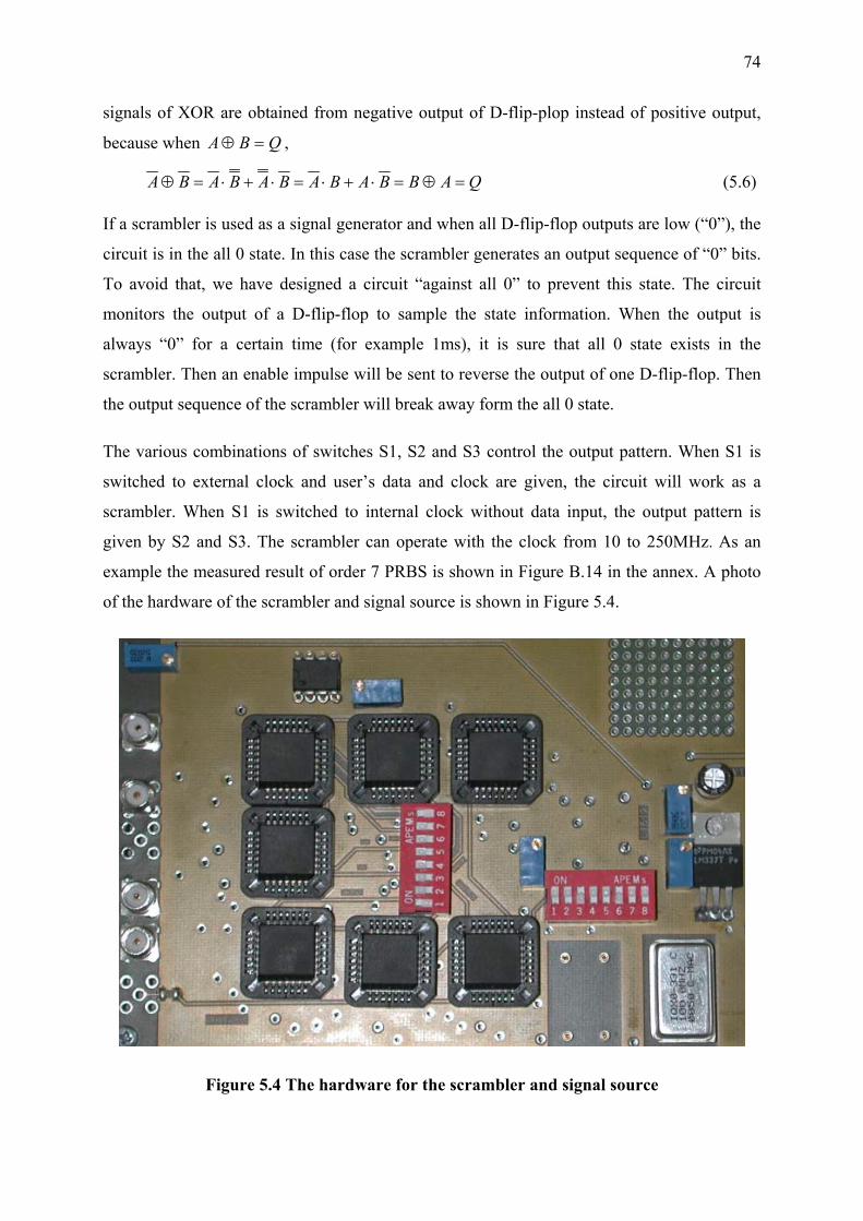
74
signals of XOR are obtained from negative output of D-flip-plop instead of positive output,
because when QBA =⊕ ,
QABBABABABABA =⊕=⋅+⋅=⋅+⋅=⊕ (5.6)
If a scrambler is used as a signal generator and when all D-flip-flop outputs are low (“0”), the
circuit is in the all 0 state. In this case the scrambler generates an output sequence of “0” bits.
To avoid that, we have designed a circuit “against all 0” to prevent this state. The circuit
monitors the output of a D-flip-flop to sample the state information. When the output is
always “0” for a certain time (for example 1ms), it is sure that all 0 state exists in the
scrambler. Then an enable impulse will be sent to reverse the output of one D-flip-flop. Then
the output sequence of the scrambler will break away form the all 0 state.
The various combinations of switches S1, S2 and S3 control the output pattern. When S1 is
switched to external clock and user’s data and clock are given, the circuit will work as a
scrambler. When S1 is switched to internal clock without data input, the output pattern is
given by S2 and S3. The scrambler can operate with the clock from 10 to 250MHz. As an
example the measured result of order 7 PRBS is shown in Figure B.14 in the annex. A photo
of the hardware of the scrambler and signal source is shown in Figure 5.4.
Figure 5.4 The hardware for the scrambler and signal source
75
5.3 Impulse Generator
Because OCDMA processing operates at chiprate, at first the users’ data has to be converted
from data rate to chiprate for CDMA coding, we design an impulse generator at transmitter to
achieve this function. For each Mark of data, this impulse generator produces a slender
impulse having a width equal to the duration of one chip, irregarding whether the Marks of
the data are continued or not. The output is the signal source of the CDMA encoders. The
impulse generator circuit needs the data and clock as inputs simultaneously. As an interface,
the line receivers for receiving of the data and the clock can be established by differential
receiver MC10EL16. This device with rise and fall times typically at 225ps is suitable for
interfacing with high frequency sources.
For the traditional method to receive data and operate it from the data rate to chiprate, the
logic diagram of impulse generator and its logic waveforms are shown in Figure 5.5. The chip
clock can be achieved from the data of the downstream in network, from the data’s clock or
from a local quartz oscillator, depending on the structure of the network. In Figure 5.5 it
comes from user’s data, and the advantage of this method is synchronism between chiprate
and user’s data rate. The “× ” is an N frequency-multiplying circuit. Here N is the length of
the codeword, that will be in detail discussed in next subchapter. D-flip-flop, AND gate and
OR gate are implemented by the IC of MC10EL series which are the fastest series for silicon
devices nowadays. The driver of the chip clock is indispensable for the D-flip-flops that work
at 2.5GHz for chiprate which is close to the limit rate for MC10EL series. Hence the chip
frequency is high, therefore the phase delay of signals in circuit design has to be considered,
that includes the delay time of logic gate and the delay time of connection line in printed
circuit board. For example, the AND gate before point A in Figure 5.5 is used as a delay gate,
in order to match the phase between the clock and the data.
N
For above mentioned scheme, the driving of two D-flip-flop with 2.5GHz and the use of
frequency-multiplier N are still not satisfying in the hardware implementation. Even if the
chip clock is generated by a local oscillator which is independent on data clock, the data
stream and the chip stream are slightly asynchronous which introduces a jitter at CDMA
processing. This jitter will affect the quality of the clock recovery at the receiver and increases
the BER.
76
Input of clock at 50MHz
A
B
C
D
E
F
G
H
Linereceiver
DLine
receiver & D
D
XOR &
1
Driver
Data in50Mb/s
Clock of chiprate
Output of Impulse
N: length of code wordD: D-flip-flopXOR: exclusive OR&: logic AND gate
A
B
C E
F
G
H
rN
Figure 5.5 The logic diagram of impulse generator and its waveform
The above mentioned two problems can be avoided by using time delay line instead of the
two high frequency D-flip-flops. Figure 5.6 shows such an improved circuit of impulse
generator and its logic waveform. The electrical delay line generates the impulse at chiprate.
Thus the generation of the chiprate clock can be avoided. The delay time of the delay line is
the duration of a chip, T . The length l of the delay line is: C
TSl ⋅= (5.7)
where S is the speed of electromagnetic wave in a coaxial line, normally it is 20cm/ns. When
is 400ps, l equals to 8cm. In practice the length is chosen to 7cm due to other phase delays
from the printed circuit board and devices.
CT
77
Linereceiver
DLine
receiver & XOR &
1
Data in50Mb/s
Input of clock at 50MHz
Output of ImpulseD: D-flip-flop XOR: exclusive OR &: logic AND gate
A
B
C
G
H
D
E
Delay line
A
B
C
D
E
G
H
Figure 5.6 The improved logic diagram of impulse generator and waveform
Data ClockData Clock
GeneratedImpulse
Figure 5.7 The output impulse of the implemented CDMA impulse generator
78
This method not only simplifies the circuit, but also has benefits for the data access. With the
circuit the impulse is generated at the start point of the data, thus the OCDMA processing will
be synchronous with the data without other conditions. This means it is possible to access
variable bit rate data into OCDMA system without increasing the phase jitter of the recovered
data clock at the receiver. The waveform of composed impulse can be seen in Figure 5.7.
5.4 Encoder/Decoder
The encoder and decoder are important parts for the CDMA processing. We have
implemented both electronic and optical encoder/decoder, respectively, in order to
demonstrate their characteristics in various schemes of OCDMA system. The structure of the
encoder and decoders are the same, i.e. using the optical or electrical delay line to compose
the codeword.
5.4.1 The Codeword
OOC code widely used in OCDMA [16] is chosen as signature code for this demonstration
system. This code can be employed to support both equal-rate and variable-rate/multi-rate
users without changing CDMA encoders and decoders.
Table 5.1 Some shortest OOC [14]
Code weight ( w)
number of users (N)
OOC of equal length ( ) CL
OOC of variable length
3 3 19; 1,2,9 19; 1,3,6 19, 1,5,11
16; 1,2,6 19; 1,3,9 21; 1,4,11
4 4 49; 1,2,21,24 49; 1,3,14,18 49; 1,6,13,22 49; 1,7,15,25
42; 1,3,14,18 46; 1,6,13,22 48; 1,2,21,24 49; 1,7,15,25
The Table 5.1 lists some codewords of shortest OOC with auto-correlation 1=aλ and cross-
correlation [14], where w is code weight, N is the maximum number of users for this
codeword family. The code length is the minimal number of chip positions for the
codewords. The numbers after the code length are the positions of “1” chips within the
CL
1=cλ
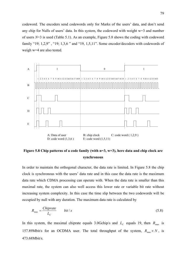
79
codeword. The encoders send codewords only for Marks of the users’ data, and don’t send
any chip for Nulls of users’ data. In this system, the codeword with weight w=3 and number
of users N=3 is used (Table 5.1). As an example, Figure 5.8 shows the coding with codeword
family “19; 1,2,9” , “19; 1,3,6 ” and “19, 1,5,11”. Some encoder/decoders with codewords of
weigh w=4 are also tested.
1 0 1
1 2 3 4 5 6 7 8 9 10 11 12 13 1415 16 17 1819 1 2 3 4 5 6 7 8 9 10 11 12 13 1415 1617 18 19 1 2 3 4 5 6 7 8 9 10 11 12 13 1415
A
B
C
D
E
A: Data of user B: chip clock C: code word ( 1,2,9 )D: code word (1,3,6 ) E: code word (1,5,11)
Figure 5.8 Chip patterns of a code family (with n=3, w=3), here data and chip clock are
synchronous
In order to maintain the orthogonal character, the data rate is limited. In Figure 5.8 the chip
clock is synchronous with the users’ data rate and in this case the data rate is the maximum
data rate which CDMA processing can operate with. When the data rate is smaller than this
maximal rate, the system can also well access this lower rate or variable bit rate without
increasing system complexity. In this case the time slip between the two codewords will be
occupied by null with any duration. The maximum data rate is calculated by
sbitL
ChiprateRC
/max = (5.8)
In this system, the maximal chiprate equals 3.0Gchip/s and equals 19, then is
157.89Mbit/s for an OCDMA user. The total throughput of the system, , is
473.68Mbit/s.
CL maxR
N×Rmax
80
5.4.2 Electronic Encoder
t1
.
.
.
Signal driver Signal adder
t2
tw
Figure 5.9 The structure of the encoder
In this demonstration system, the impulse generators are established as interfaces for user’s
data. Hence the electronic encoder of OCDMA directly operates with the stimulated signal
from impulse generators. The principle structure of the electronic or optical encoder which is
built with delay lines is shown in Figure 5.9. The left part of the structure is signal power
splitter or signal driver and the right part is signal power adder. The two parts are connected
by the electronic delay lines. Each delay line has an individual delay time, which contributes
an impulse (chip) for the codeword at output of electronic encoders. The difference between
the delay times decides the pattern of the codeword. For example, the codeword E (1,5,11) in
Figure 5.8 has the differences between delay times
C
C
TttTtt
104
13
12
=−=−
(5.9)
where T is the duration of one chip and is the inevitable time delay in the first branch
at the implementation. When chip clock is 2.5GHz, = 0.4 ns, t
C 1t
CT 12 t− = 1.6 ns and t 13 t− =
4.0 ns. Using Eq. (5.7), the length of the delay line can be calculated. In practice the real delay
times have to be fixed by the measurement, because the electrical circuit and PLC also
influence the delay time. The measurement of the delay time isn’t difficult by using a high
frequency oscilloscope with 10GHz bandwidth. Then the difference between the delay times
can be accurately adjusted. The block diagram of an electronic encoder is shown in Figure
5.10 a). By using this scheme we can implement all codewords with through
adjusting the length of the delay line. For example, Figure 5.10 a) shows the delay times of
4≤w
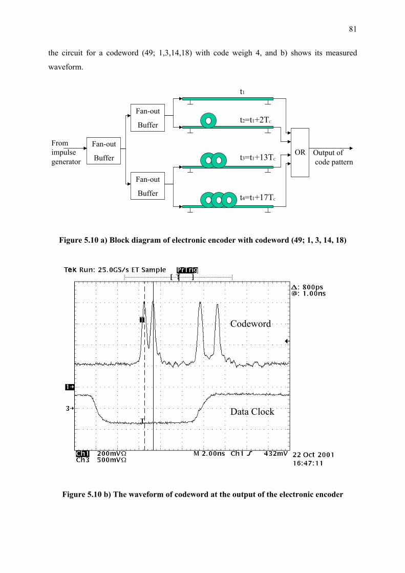
81
the circuit for a codeword (49; 1,3,14,18) with code weigh 4, and b) shows its measured
waveform.
Fan-out
Buffer
Fan-out
Buffer
Fan-out
Buffer
ORFromimpulse generator
Output of code pattern
t1
t2=t1+2TC
t3=t1+13TC
t4=t1+17TC
Figure 5.10 a) Block diagram of electronic encoder with codeword (49; 1, 3, 14, 18)
Codeword
Data Clock
Figure 5.10 b) The waveform of codeword at the output of the electronic encoder
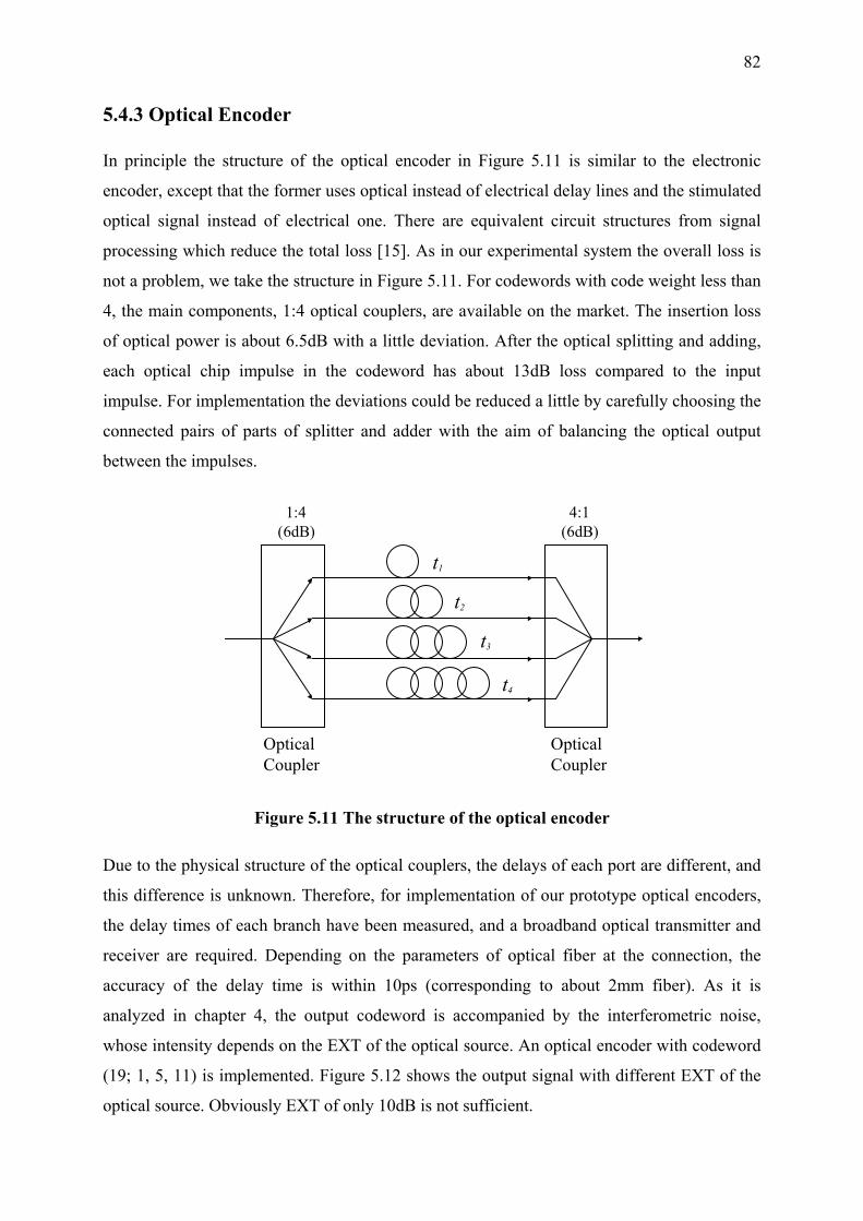
82
5.4.3 Optical Encoder
In principle the structure of the optical encoder in Figure 5.11 is similar to the electronic
encoder, except that the former uses optical instead of electrical delay lines and the stimulated
optical signal instead of electrical one. There are equivalent circuit structures from signal
processing which reduce the total loss [15]. As in our experimental system the overall loss is
not a problem, we take the structure in Figure 5.11. For codewords with code weight less than
4, the main components, 1:4 optical couplers, are available on the market. The insertion loss
of optical power is about 6.5dB with a little deviation. After the optical splitting and adding,
each optical chip impulse in the codeword has about 13dB loss compared to the input
impulse. For implementation the deviations could be reduced a little by carefully choosing the
connected pairs of parts of splitter and adder with the aim of balancing the optical output
between the impulses.
t1
1:4(6dB)
4:1(6dB)
OpticalCoupler
OpticalCoupler
t2
t3
t4
Figure 5.11 The structure of the optical encoder
Due to the physical structure of the optical couplers, the delays of each port are different, and
this difference is unknown. Therefore, for implementation of our prototype optical encoders,
the delay times of each branch have been measured, and a broadband optical transmitter and
receiver are required. Depending on the parameters of optical fiber at the connection, the
accuracy of the delay time is within 10ps (corresponding to about 2mm fiber). As it is
analyzed in chapter 4, the output codeword is accompanied by the interferometric noise,
whose intensity depends on the EXT of the optical source. An optical encoder with codeword
(19; 1, 5, 11) is implemented. Figure 5.12 shows the output signal with different EXT of the
optical source. Obviously EXT of only 10dB is not sufficient.
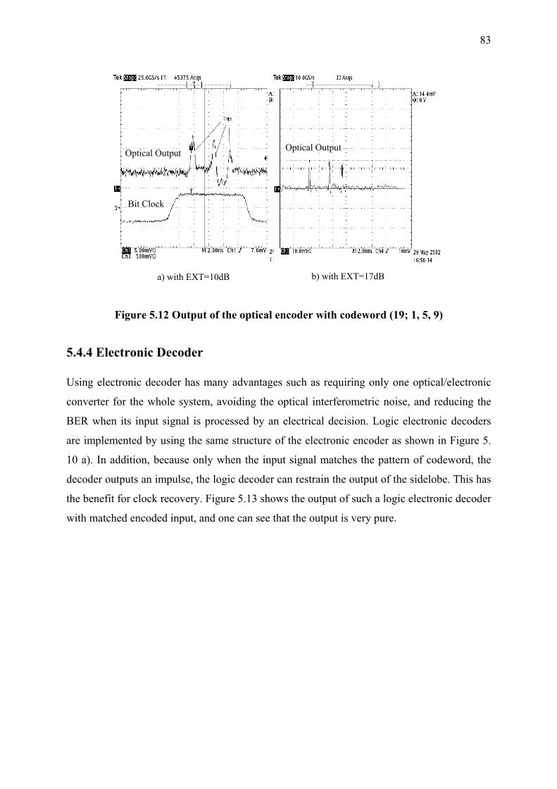
83
a) with EXT=10dB b) with EXT=17dB
Optical Output
Bit Clock
Optical Output
Figure 5.12 Output of the optical encoder with codeword (19; 1, 5, 9)
5.4.4 Electronic Decoder
Using electronic decoder has many advantages such as requiring only one optical/electronic
converter for the whole system, avoiding the optical interferometric noise, and reducing the
BER when its input signal is processed by an electrical decision. Logic electronic decoders
are implemented by using the same structure of the electronic encoder as shown in Figure 5.
10 a). In addition, because only when the input signal matches the pattern of codeword, the
decoder outputs an impulse, the logic decoder can restrain the output of the sidelobe. This has
the benefit for clock recovery. Figure 5.13 shows the output of such a logic electronic decoder
with matched encoded input, and one can see that the output is very pure.
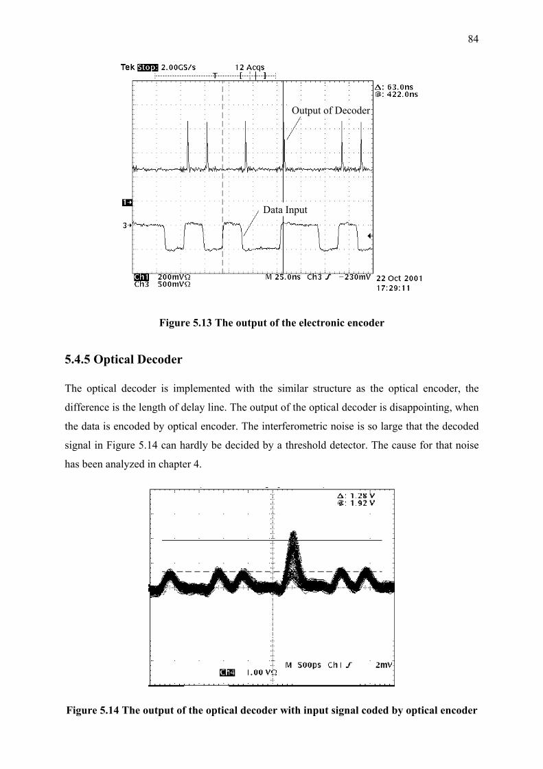
84
Output of Decoder
Data Input
Figure 5.13 The output of the electronic encoder
5.4.5 Optical Decoder
The optical decoder is implemented with the similar structure as the optical encoder, the
difference is the length of delay line. The output of the optical decoder is disappointing, when
the data is encoded by optical encoder. The interferometric noise is so large that the decoded
signal in Figure 5.14 can hardly be decided by a threshold detector. The cause for that noise
has been analyzed in chapter 4.
Figure 5.14 The output of the optical decoder with input signal coded by optical encoder
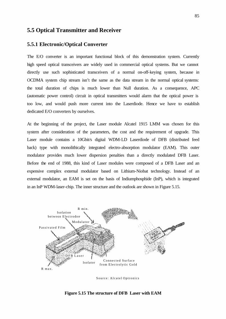
85
5.5 Optical Transmitter and Receiver
5.5.1 Electronic/Optical Converter
The E/O converter is an important functional block of this demonstration system. Currently
high speed optical transceivers are widely used in commercial optical systems. But we cannot
directly use such sophisticated transceivers of a normal on-off-keying system, because in
OCDMA system chip stream isn’t the same as the data stream in the normal optical systems:
the total duration of chips is much lower than Null duration. As a consequence, APC
(automatic power control) circuit in optical transmitters would alarm that the optical power is
too low, and would push more current into the Laserdiode. Hence we have to establish
dedicated E/O converters by ourselves.
At the beginning of the project, the Laser module Alcatel 1915 LMM was chosen for this
system after consideration of the parameters, the cost and the requirement of upgrade. This
Laser module contains a 10Gbit/s digital WDM-LD Laserdiode of DFB (distributed feed
back) type with monolithically integrated electro-absorption modulator (EAM). This outer
modulator provides much lower dispersion penalties than a directly modulated DFB Laser.
Before the end of 1988, this kind of Laser modules were composed of a DFB Laser and an
expensive complex external modulator based on Lithium-Niobat technology. Instead of an
external modulator, an EAM is set on the basis of Indiumphosphide (InP), which is integrated
in an InP WDM-laser-chip. The inner structure and the outlook are shown in Figure 5.15.
S o u r c e : A l c a t e l O p t r o n i c s
Isola tor
R m a x . R m a x .
R m i n .
P a s s i v a t e d F i lm
M o d u l a t o r
D F B L a s e rC o n n e c t e d S u r f a c e
f rom Elec t ro ly t i c Go ld
Isolat ionbe tween E lec t rodes
Figure 5.15 The structure of DFB Laser with EAM
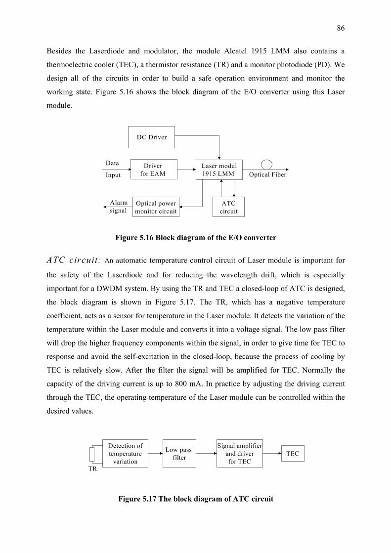
86
Besides the Laserdiode and modulator, the module Alcatel 1915 LMM also contains a
thermoelectric cooler (TEC), a thermistor resistance (TR) and a monitor photodiode (PD). We
design all of the circuits in order to build a safe operation environment and monitor the
working state. Figure 5.16 shows the block diagram of the E/O converter using this Laser
module.
DC Driver
Laser modul1915 LMM Optical Fiber
Optical powermonitor circuit
ATCcircuit
Data
Input
Alarmsignal
Driver for EAM
Figure 5.16 Block diagram of the E/O converter
ATC circuit: An automatic temperature control circuit of Laser module is important for
the safety of the Laserdiode and for reducing the wavelength drift, which is especially
important for a DWDM system. By using the TR and TEC a closed-loop of ATC is designed,
the block diagram is shown in Figure 5.17. The TR, which has a negative temperature
coefficient, acts as a sensor for temperature in the Laser module. It detects the variation of the
temperature within the Laser module and converts it into a voltage signal. The low pass filter
will drop the higher frequency components within the signal, in order to give time for TEC to
response and avoid the self-excitation in the closed-loop, because the process of cooling by
TEC is relatively slow. After the filter the signal will be amplified for TEC. Normally the
capacity of the driving current is up to 800 mA. In practice by adjusting the driving current
through the TEC, the operating temperature of the Laser module can be controlled within the
desired values.
Detection oftemperature
variation
Low pass filter
Signal amplifier and driver
for TECTEC
TR
Figure 5.17 The block diagram of ATC circuit
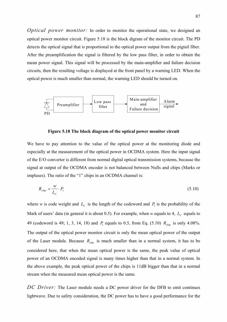
87
Optical power monitor: In order to monitor the operational state, we designed an
optical power monitor circuit. Figure 5.18 is the block digram of the monitor circuit. The PD
detects the optical signal that is proportional to the optical power output from the pigtail fiber.
After the preamplification the signal is filtered by the low pass filter, in order to obtain the
mean power signal. This signal will be processed by the main-amplifier and failure decision
circuits, then the resulting voltage is displayed at the front panel by a warning LED. When the
optical power is much smaller than normal, the warning LED should be turned on.
PreamplifierLow pass
filter
Main-amplifierand
Failure decisionPD
Alarmsignal
Figure 5.18 The block diagram of the optical power monitor circuit
We have to pay attention to the value of the optical power at the monitoring diode and
especially at the measurement of the optical power in OCDMA system. Here the input signal
of the E/O converter is different from normal digital optical transmission systems, because the
signal at output of the OCDMA encoder is not balanced between Nulls and chips (Marks or
impluses). The ratio of the “1” chips in an OCDMA channel is:
1PLwR
Cchip ⋅= (5.10)
where w is code weight and is the length of the codeword and is the probability of the
Mark of users’ data (in general it is about 0.5). For example, when w equals to 4, equals to
49 (codeword is 49; 1, 3, 14, 18) and equals to 0.5, from Eq. (5.10) is only 4.08%.
The output of the optical power monitor circuit is only the mean optical power of the output
of the Laser module. Because is much smaller than in a normal system, it has to be
considered here, that when the mean optical power is the same, the peak value of optical
power of an OCDMA encoded signal is many times higher than that in a normal system. In
the above example, the peak optical power of the chips is 11dB bigger than that in a normal
stream when the measured mean optical power is the same.
CL 1P
CL
1P chipR
chipR
DC Driver: The Laser module needs a DC power driver for the DFB to emit continues
lightwave. Due to safety consideration, the DC power has to have a good performance for the
88
on and off operation, i.e. it has very slow rise time and fall time without impulse and tide to
avoid harm the LD. Consider that the maximum forward voltage of the Laserdiode is 2V and
the maximum forward current is 150mA, we designed a circuit to fulfill this function as
shown in Figure 5.19. LM317 is a 3-terminal adjustable regulator that is capable of supplying
a 1.2V to 37V output range. They are very easy to use and require only two external resistors
to set the output voltage. Here the power supply is 10V, then the voltage at point A is set to be
6 V by adjusting R1. T1, R5 and C1 compose the slow starting circuit. When R5 is big
enough, it generates a relative long time to charge the big capacitor C1. IC2 and R2 compose
a precision current limiter, the current is limited to:
2lim
45.1R
VVVI BA −−
= (5.11)
IC3, R3 and R6 compose the adjustable regulator, which limit the voltage of the output. D1 is
a diode for protecting the Laserdiode against reverse current in case of accident. R7 is a
resistor for limiting the current, in practice to 60mA. When the Laserdiode operates with a
current of 33mA, the optical output power is +0.7dBm.
LM317 LM317 LM317input output
R1T1
C1
R2
R3D1
R4
R5
R6
IC1 IC2 IC3
R1=1KΩ R2=100Ω R3=500ΩR4,R6 =240Ω R5=50kΩ C1=100ηF
A B
10V
C R7
Figure 5.19 The circuit for DC power adjustment of DFB Laser
Driver for EAM: We used FMM311 GaAs Laser driver by Fujitsu as the high frequency
driver for electro-absorption modulator. FMM311 is a high-data rate driver circuit designed
for fiber optic transmitters operating at data rates up to 2.7Gbit/s. The device is capable of
driving high-power Laserdiodes at peak current up to 80mA, typically. The block diagram of
laser driver circuit is shown in Figure 5.20 (a), and the high frequency equivalent is shown in
Figure 5.20 (b).
89
EA
LD
(a) (b)
Driver
IRLR IR
LR
50ΩCoaxial line ecodeE
DI oVoV
DI
Figure 5. 20 (a) Block diagram of driver and Laser module; (b) the high frequency
equivalent
Note that the output of the FMM311 is a current source instead of a voltage source required
by the EAM in Laser module. The output voltage V is given by 0
DLI
LI IRRRRV
+⋅
≈0 (5.12)
where is the load resistor of coaxial cable which equals to 50Ω, and is a resistor at the
driver side. When is also selected as 50Ω, the result is:
LR IR
IR
DIV ⋅Ω= 250 (5.13)
For example, when is limited to 60mA, the maximum V is 1.5V. DI 0
0 0.5 1 1.5 2 2.5 3−30
−25
−20
−15
−10
−5
0
5
10dB
V
The input voltage at the EAM
The
optic
al a
bsor
ptio
n
Figure 5.21 The optical absorption capacity versus the input voltage at the EAM of
Alcatel 1915 LMM
90
From the analysis in chapter 4, for optical encoder the EXT has to be larger than 17dB. For
A1915LMM Laser module, it is difficult to reach this value. This is related to the
characteristic of EAM, the function curve of which is shown in Figure 5.21. The maximum
EXT of A1915LMM is only 14dB, so this optical modulator can not be used in OCDMA
transmitter with optical encoder, because large interferometric noise will occur at the output
of the optical encoder. In order to demonstrate the OCDMA processing with both optical
encoder and optical decoder, we also implement the O/E converters with directly modulated
DFB-Laser module, A1915 LMI. The block diagram of its structure is shown in Figure 5.22.
The function blocks are almost the same as those in A1915LMM. Here EXT can reach 30dB.
Laser driver Laser moduleOptical Fiber
Optical powermonitor circuit
ATCcircuit
Input
Alarmsignal
Figure 5.22 The structure of the O/E converter with direct modulation Laser module
After optimizing and testing, we have implemented the E/O converter with good performance
and safety.
5.5.2 Optical Receiver
The optical receiver of OCDMA system consists of O/E converter, electronic amplifier and
decision as in usual systems.
O/E Converter: In this system we use an Agilent 11982A amplified lightwave converter
as the optical/electronic converter. It combines a PIN photodetector with a low noise
preamplifier and is a sensitive O/E converter with wide bandwidth. Agilent 11982A covers
the wavelengths from 1.200nm to 1.600nm and bandwidths from DC to 12GHz. Its 300
volts/watt conversion gain and 0.05% input optical reflection significantly improve sensitivity
for the system.
Amplifiers: The electronic signal from O/E converter will be amplified by broadband
amplifiers. The Model 5850 ultra-broadband amplifiers produced by Picosecond are selected
due to the attractive price/performance ratio. They are AC coupled and are extremely
broadband covering the range of 5 decades from 80kHz to 5GHz. They have clean transient
91
responses and smooth gain vs. frequency responses. In practice, due to the AC coupling of the
amplifiers and unbalance of the signal waveforms, the gains and output range of the
amplifiers are not fully used. The amplifiers must be connected in cascade for higher gains
and in this case the noise is increased. Because the Model 5850 Amplifier is a static-sensitive
device, static discharge must be avoided.
Decision: After being amplified, the signal of receiver will be decided in order to convert
analog signal into digital signal for electronic decoders. Nowadays we can not find on the
market a suitable decision device that operates at 2.5G chips/s. Hence we use a logic gate with
a short rise/fall time of 150ps as a decision element. The level of decision is important for the
correct transmission. We use a high speed ECL IC with two inverse inputs, one is the input of
the analog received signal, and the other is the DC level for offsetting the threshold which
could be reset when the structure of the system is changed.
5.6 Data Recovery
Data recovery is composed of clock recovery and the data sampling. The decoded signal is
despreaded into a series of impulses, in which not all of them means Marks of desired user’s
data. There are many noise impulses produced by the other users’ interference, which mostly
locate at the fail position (when the position is right, it could be the source of the bit errors).
Hence there are two difficult points at the data recovery of the OCDMA system: one is
restoring clock from signal with fail information and the jitter of the clock must be much
lower than the chip duration in order to correctly sample the very slim auto-correction
impulse; the other is adjusting the sampling time at the center of the auto-correction impulse
in order to avoid the phase swing of the restored clock by the temperature.
5.6.1 Clock Recovery
The clock recovery is achieved by using a phase locked loop (PLL) circuit. The basic block
diagram of the structure is shown in Figure 5.23 a). During the implementation of the PLL
circuit, in order to achieve a clock with low jitter, three measures are taken in the design.
Firstly, an impulse processing circuit is used to shape and broaden the impulses. After
broadening of the impulse, the bandwidth of the signal is reduced, so the phase detector can
operate at relatively low frequency. Secondly, the voltage controlled oscillator (VCO)
operates at multiple frequencies of the clock, therefore PLL is more sensitive for the
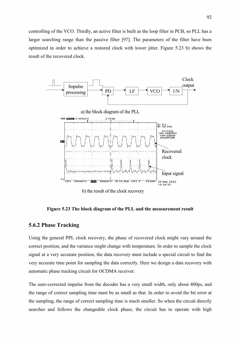
92
controlling of the VCO. Thirdly, an active filter is built as the loop filter in PCB, so PLL has a
larger searching range than the passive filter [97]. The parameters of the filter have been
optimized in order to achieve a restored clock with lower jitter. Figure 5.23 b) shows the
result of the recovered clock.
Impulseprocessing PD LF VCO
Clockoutput
1/N
a) the block diagram of the PLL
b) the result of the clock recovery
Input signal
Recoveredclock
Figure 5.23 The block diagram of the PLL and the measurement result
5.6.2 Phase Tracking
Using the general PPL clock recovery, the phase of recovered clock might vary around the
correct position, and the variance might change with temperature. In order to sample the clock
signal at a very accurate position, the data recovery must include a special circuit to find the
very accurate time point for sampling the data correctly. Here we design a data recovery with
automatic phase tracking circuit for OCDMA receiver.
The auto-corrected impulse from the decoder has a very small width, only about 400ps, and
the range of correct sampling time must be as small as that. In order to avoid the bit error at
the sampling, the range of correct sampling time is much smaller. So when the circuit directly
searches and follows the changeable clock phase, the circuit has to operate with high
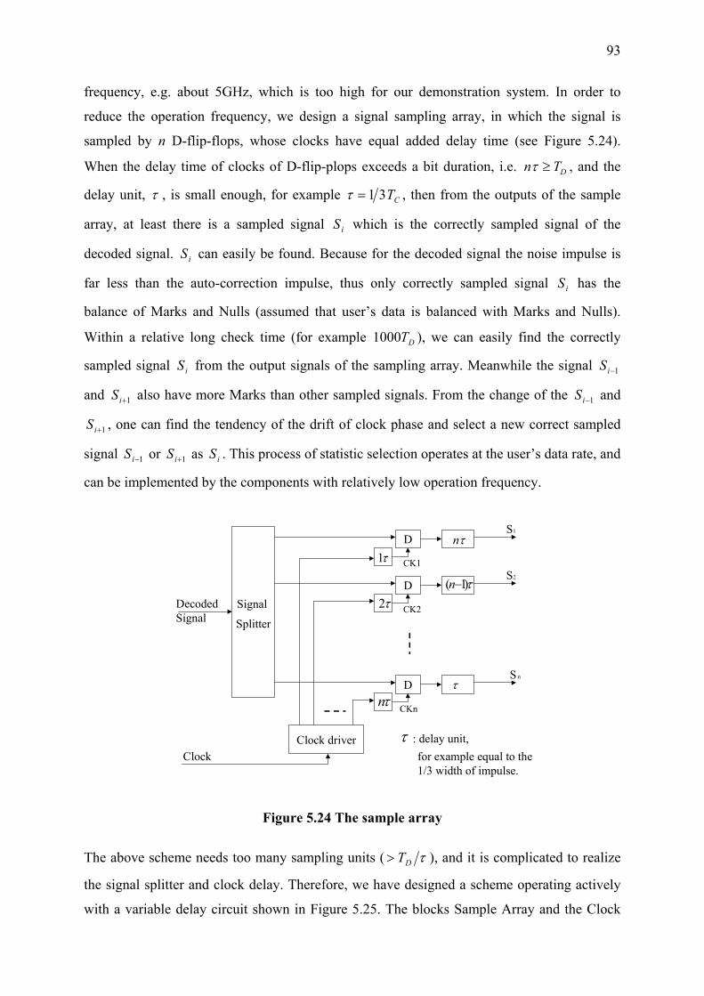
93
frequency, e.g. about 5GHz, which is too high for our demonstration system. In order to
reduce the operation frequency, we design a signal sampling array, in which the signal is
sampled by n D-flip-flops, whose clocks have equal added delay time (see Figure 5.24).
When the delay time of clocks of D-flip-plops exceeds a bit duration, i.e. DTn ≥τ , and the
delay unit, τ , is small enough, for example CT31=τ , then from the outputs of the sample
array, at least there is a sampled signal which is the correctly sampled signal of the
decoded signal. can easily be found. Because for the decoded signal the noise impulse is
far less than the auto-correction impulse, thus only correctly sampled signal has the
balance of Marks and Nulls (assumed that user’s data is balanced with Marks and Nulls).
Within a relative long check time (for example 1000 ), we can easily find the correctly
sampled signal from the output signals of the sampling array. Meanwhile the signal
and also have more Marks than other sampled signals. From the change of the and
, one can find the tendency of the drift of clock phase and select a new correct sampled
signal or as . This process of statistic selection operates at the user’s data rate, and
can be implemented by the components with relatively low operation frequency.
iS
iS
iS
1+
iS
DT
1−iS
1+iS
iS
1−iS
1+iS
1− iS iS
Signal
Splitter
D
D
D
Clock driver : delay unit,Clock
DecodedSignal
S1
S2
S n
for example equal to the1/3 width of impulse.
CK1
CK2
CKn
τ2
τ1
τn
τn
τ)1( −n
τ
τ
Figure 5.24 The sample array
The above scheme needs too many sampling units ( τDT> ), and it is complicated to realize
the signal splitter and clock delay. Therefore, we have designed a scheme operating actively
with a variable delay circuit shown in Figure 5.25. The blocks Sample Array and the Clock
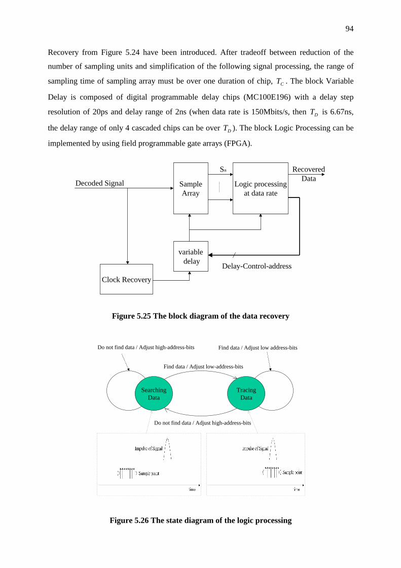
94
Recovery from Figure 5.24 have been introduced. After tradeoff between reduction of the
number of sampling units and simplification of the following signal processing, the range of
sampling time of sampling array must be over one duration of chip, CT . The block Variable
Delay is composed of digital programmable delay chips (MC100E196) with a delay step
resolution of 20ps and delay range of 2ns (when data rate is 150Mbits/s, then DT is 6.67ns,
the delay range of only 4 cascaded chips can be over DT ). The block Logic Processing can be
implemented by using field programmable gate arrays (FPGA).
SampleArray
Logic processingat data rate
Clock Recovery
variable delay
Decoded Signal
RecoveredData
Delay-Control-address
Sn
Figure 5.25 The block diagram of the data recovery
SearchingData
TracingData
Find data / Adjust low-address-bits
Do not find data / Adjust high-address-bits
Find data / Adjust low address-bitsDo not find data / Adjust high-address-bits
Figure 5.26 The state diagram of the logic processing
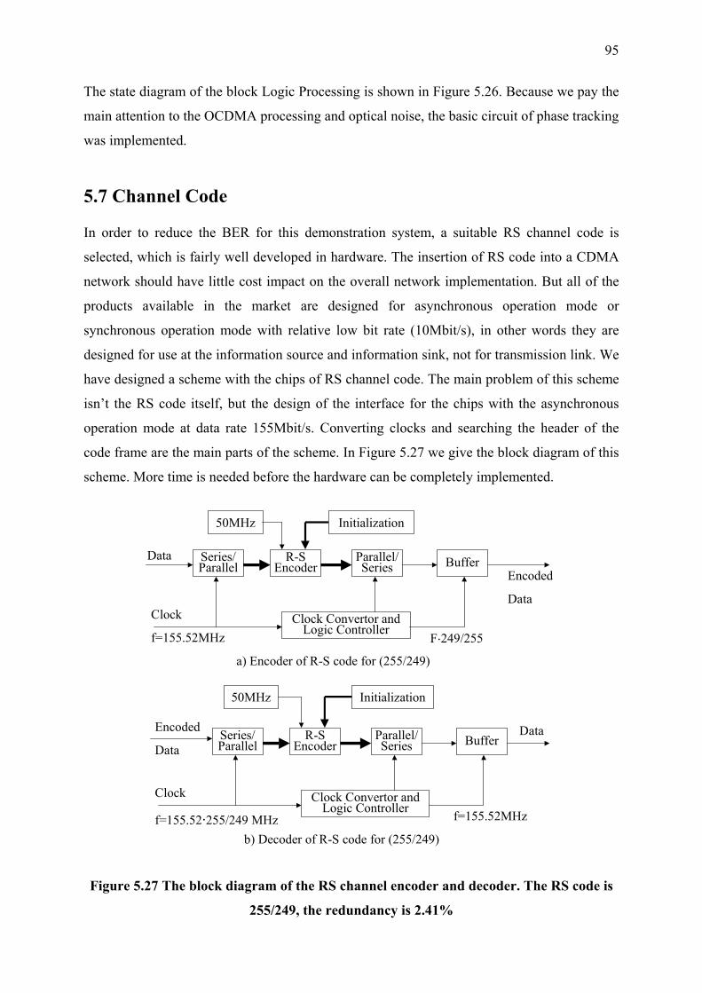
95
The state diagram of the block Logic Processing is shown in Figure 5.26. Because we pay the
main attention to the OCDMA processing and optical noise, the basic circuit of phase tracking
was implemented.
5.7 Channel Code
In order to reduce the BER for this demonstration system, a suitable RS channel code is
selected, which is fairly well developed in hardware. The insertion of RS code into a CDMA
network should have little cost impact on the overall network implementation. But all of the
products available in the market are designed for asynchronous operation mode or
synchronous operation mode with relative low bit rate (10Mbit/s), in other words they are
designed for use at the information source and information sink, not for transmission link. We
have designed a scheme with the chips of RS channel code. The main problem of this scheme
isn’t the RS code itself, but the design of the interface for the chips with the asynchronous
operation mode at data rate 155Mbit/s. Converting clocks and searching the header of the
code frame are the main parts of the scheme. In Figure 5.27 we give the block diagram of this
scheme. More time is needed before the hardware can be completely implemented.
F.249/255
Series/Parallel
R-SEncoder
Parallel/Series Buffer
Clock
f=155.52MHzClock Convertor and
Logic Controller
DataEncoded
Data
50MHz Initialization
b) Decoder of R-S code for (255/249)
Clock
f=155.52.255/249 MHz
DataEncoded
Data
f=155.52MHz
Series/Parallel
R-SEncoder
Parallel/Series Buffer
Clock Convertor andLogic Controller
50MHz Initialization
a) Encoder of R-S code for (255/249)
Figure 5.27 The block diagram of the RS channel encoder and decoder. The RS code is
255/249, the redundancy is 2.41%
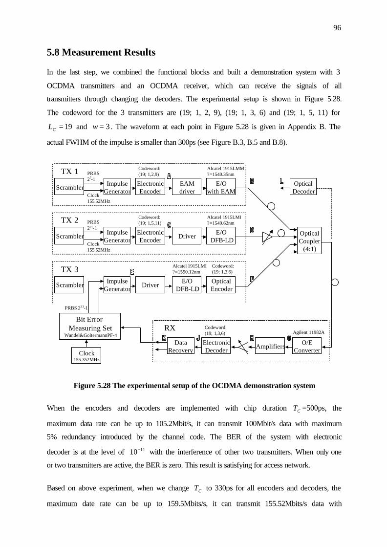
96
5.8 Measurement Results
In the last step, we combined the functional blocks and built a demonstration system with 3
OCDMA transmitters and an OCDMA receiver, which can receive the signals of all
transmitters through changing the decoders. The experimental setup is shown in Figure 5.28.
The codeword for the 3 transmitters are (19; 1, 2, 9), (19; 1, 3, 6) and (19; 1, 5, 11) for
19=CL and 3=w . The waveform at each point in Figure 5.28 is given in Appendix B. The
actual FWHM of the impulse is smaller than 300ps (see Figure B.3, B.5 and B.8).
Bit Error Measuring Set
Wandel&GoltermannPF-4
PRBS27-1
Clock155.52MHz
PRBS 223-1
TX 1Impulse
Generator
Codeword:(19; 1,2,9)
Alcatel 1915LMM?=1540.35nm
ElectronicEncoder
EAMdriver
E/Owith EAMScrambler
PRBS221-1
Clock155.52MHz
TX 2Impulse
Generator
Codeword:(19; 1,5,11)
Alcatel 1915LMI?=1549.62nm
ElectronicEncoder Driver E/O
DFB-LDScrambler
TX 3Impulse
Generator
Codeword:(19; 1,3,6)
OpticalEncoderDriver E/O
DFB-LDScrambler
Alcatel 1915LMI?=1550.12nm
OpticalCoupler
(4:1)
Clock155.352MHz
RX
DataRecovery
Codeword:(19; 1,3,6)
O/EConverter
ElectronicDecoder Amplifiers
Agilent 11982A
OpticalDecoder
Figure 5.28 The experimental setup of the OCDMA demonstration system
When the encoders and decoders are implemented with chip duration CT =500ps, the
maximum data rate can be up to 105.2Mbit/s, it can transmit 100Mbit/s data with maximum
5% redundancy introduced by the channel code. The BER of the system with electronic
decoder is at the level of 1110− with the interference of other two transmitters. When only one
or two transmitters are active, the BER is zero. This result is satisfying for access network.
Based on above experiment, when we change CT to 330ps for all encoders and decoders, the
maximum date rate can be up to 159.5Mbits/s, it can transmit 155.52Mbits/s data with
97
maximum 2.55% redundancy of channel code. The BER at this data rate is only 10 . The
reason of high BER is that the impulse is not slim enough for T . This verifies that
FWHM of the impulse must be smaller than the theoretical chip duration for BER free
system.
5−
psC 330=
For this demonstration system, because the number of users is only 3, and the code weight is
3, the interference of the other users can not produce severe noise impulses. A failure impulse
only exists when the desired data is Mark, i.e. the noise impulses depend of the data signal. So
the requirements for the clock and its phase are not strict.
From the measurements, it is noted that the OCDMA system is not as sensitive to the
transmission of long strings of NRZ “1” bits of users’ data as in normal optical system. The
BER is almost the same when the transmission data pattern is all “1”, PRBS or 010101
sequence, respectively. The reason is that the transmission band is independent on the pattern
of data, but it depends on the CDMA processing.
Through this experimental system, the possibility of using OCDMA with electronic
en/decoding process in access network has been demonstrated.
98
Chapter 6 OCDMA Combined with DWDM
As it has been shown from the results of the analysis and demonstration system, OCDMA
technology with electronic encoder and decoder can be easily implemented within a narrow
optical spectrum, hence it is possible to insert an OCDMA group into a WDM channel. When
OCDM and DWDM are combined in access network, by using todays mature technology, the
number of accessed users and the throughput can satisfy the demand easily. In this chapter we
will discuss the feasibility of the OCDMA/DWDM system. At first the development of
DWDM will be reviewed, then the noise in OCDMA/DWDM system will be calculated and
its performances will be evaluated. Finally an example of system structure will be given.
6.1 The Fundamentals of WDM
By using WDM two or more optical signals having different wavelengths may be combined
and simultaneously transmitted in the same direction over one fiber. These signals are then
separated by wavelength at the distant end. Distinguishing from the coarse WDM (CWDM),
dense WDM (DWDM) is a technology that can increase capacity of a fiber span by many
folds. The wavelengths implemented by DWDM are located in two different bands, i.e. C
band (1529–1541nm) and L band (1549–1577nm). Current DWDM systems can carry 80
channels [86] and systems supporting more than 250 channels have been reported [85]. Each
channel could operate at up to 10Gbit/s or even 40Gbit/s.
Since WDM is a protocol-independent technology, it could be used in almost all network
architectures, such as ATM over DWDM and IP over DWDM. Certainly OCDMA could be
also easily combined with DWDM, when spectrum of each OCDMA group is within a
DWDM transmission band. Because of the high cost, early implementations of WDM systems
are limited to backbone network. However, new developments in materials and techniques
allows manufacturers to reduce the cost of WDM systems significantly. As a result, WDM
system begins to appear in MANs and LANs.
In DWDM system, optical filters are the critical components, the characteristics of which
determine the performance of DWDM. Different types of optical filters can be used in
yjzhang
S band 1500-1530
99
DWDM systems, such as Fabry-Perot filters, grating filters, interference filters, etc. We will
not go into details of the structure on these devices, since they can be simulated according to
their characteristics. We only pay attention to the results of the filtering.
Generally this kind of devices can be simulated by means of transfer function H(ν). For
instance the transfer function of a Fabry-Perot filter can be written as [88]
∆−
−
−=
νννπ
ν)(2exp1
1)(0iR
RH FP (6.1)
where is the reflectivity of the interferometer mirrors and ∆ν is the spacing between
adjacent resonant frequencies. To obtain a good quality filter, the interferometer loss has to be
small, this implies 1-
0>R
R <<1. In this approximation, the 3-dB bandwidth of the Fabry-Perot
filter, Bo, is given by
νπ
∆−
=RRBo
1 (6.2)
Generally, the factor )/()1( RR π−=ℑ , that depends only on the reflectivity of the mirrors,
is called filter finesse. So the filter is characterized by the free spectral range ∆ν and the
finesse . ℑ
Around a given resonance peak the transfer function of a Fabry-Perot filter can be
approximated by a Lorentzian function:
0
0 )(1
1)(
Bi
H FP ννν
−−
≈ (6.3)
The demand for bandwidth has accelerated the deployment of DWDM filters. Besides the
Fabry-Perot filter, the Fiber Bragg Grating filter which features flat top response with steep
spectral skirt also represents a key element in fiber optical communication systems. Due to
their fabrication process, they have very low insertion loss, immunity against electromagnetic
interference, electrical isolation and light weight. DWDM gratings can be designed for
channel separations down to 25GHz and used to select the different wavelengths of the grid.
However, for the application in access network with large access number, the use of WDM
would require special steady optical source and narrowband optical filters. The smaller the
bandwidth, the stricter the parameters of components have to be.
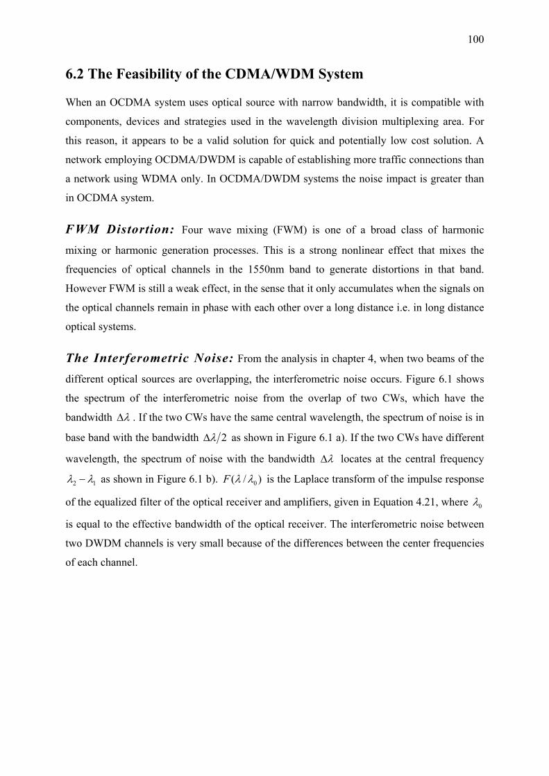
100
6.2 The Feasibility of the CDMA/WDM System
When an OCDMA system uses optical source with narrow bandwidth, it is compatible with
components, devices and strategies used in the wavelength division multiplexing area. For
this reason, it appears to be a valid solution for quick and potentially low cost solution. A
network employing OCDMA/DWDM is capable of establishing more traffic connections than
a network using WDMA only. In OCDMA/DWDM systems the noise impact is greater than
in OCDMA system.
FWM Distortion: Four wave mixing (FWM) is one of a broad class of harmonic
mixing or harmonic generation processes. This is a strong nonlinear effect that mixes the
frequencies of optical channels in the 1550nm band to generate distortions in that band.
However FWM is still a weak effect, in the sense that it only accumulates when the signals on
the optical channels remain in phase with each other over a long distance i.e. in long distance
optical systems.
The Interferometric Noise: From the analysis in chapter 4, when two beams of the
different optical sources are overlapping, the interferometric noise occurs. Figure 6.1 shows
the spectrum of the interferometric noise from the overlap of two CWs, which have the
bandwidth λ∆ . If the two CWs have the same central wavelength, the spectrum of noise is in
base band with the bandwidth 2λ∆ as shown in Figure 6.1 a). If the two CWs have different
wavelength, the spectrum of noise with the bandwidth λ∆ locates at the central frequency
12 λλ − as shown in Figure 6.1 b). )/( 0λλF is the Laplace transform of the impulse response
of the equalized filter of the optical receiver and amplifiers, given in Equation 4.21, where 0λ
is equal to the effective bandwidth of the optical receiver. The interferometric noise between
two DWDM channels is very small because of the differences between the center frequencies
of each channel.
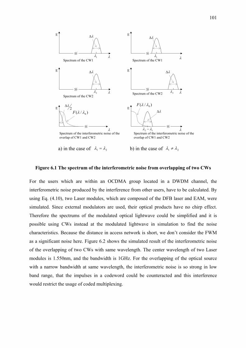
101
E
E
Spectrum of the CW1
Spectrum of the CW2
E
Spectrum of the interferometric noise of theoverlap of CW1 and CW2
E
E
Spectrum of the CW1
Spectrum of the CW2
E
Spectrum of the interferometric noise of theoverlap of CW1 and CW2
λ∆
λ∆
λ∆
λ∆
2λ∆
λ
λ
λ λ
λ
λ1λ
2λ
1λ
2λ
12 λλ −
)/( 0λλFλ∆
a) in the case of 21 λλ = b) in the case of 21 λλ ≠
)/( 0λλF
Figure 6.1 The spectrum of the interferometric noise from overlapping of two CWs
For the users which are within an OCDMA group located in a DWDM channel, the
interferometric noise produced by the interference from other users, have to be calculated. By
using Eq. (4.10), two Laser modules, which are composed of the DFB laser and EAM, were
simulated. Since external modulators are used, their optical products have no chirp effect.
Therefore the spectrums of the modulated optical lightwave could be simplified and it is
possible using CWs instead at the modulated lightwave in simulation to find the noise
characteristics. Because the distance in access network is short, we don’t consider the FWM
as a significant noise here. Figure 6.2 shows the simulated result of the interferometric noise
of the overlapping of two CWs with same wavelength. The center wavelength of two Laser
modules is 1.550nm, and the bandwidth is 1GHz. For the overlapping of the optical source
with a narrow bandwidth at same wavelength, the interferometric noise is so strong in low
band range, that the impulses in a codeword could be counteracted and this interference
would restrict the usage of coded multiplexing.
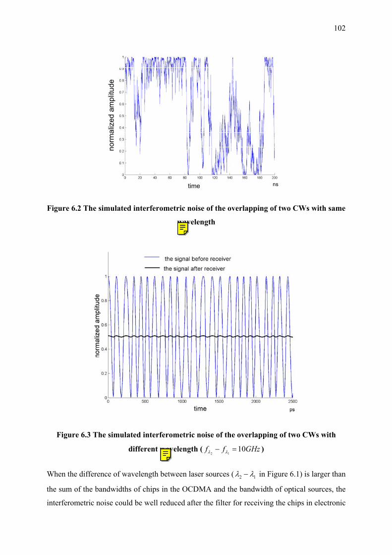
102
time
norm
aliz
ed a
mpl
itude
ns
Figure 6.2 The simulated interferometric noise of the overlapping of two CWs with same
wavelength
Figure 6.3 The simulated interferometric noise of the overlapping of two CWs with
different wavelength ( GHzff 1012=− λλ )
When the difference of wavelength between laser sources ( 12 λλ − in Figure 6.1) is larger than
the sum of the bandwidths of chips in the OCDMA and the bandwidth of optical sources, the
interferometric noise could be well reduced after the filter for receiving the chips in electronic
yjzhang
Matlab: laser2.m
yjzhang
Matlab: laser3.m
103
domain. In OCDMA/DWDM system, the wavelength of optical sources for one OCDMA
group have to be well chosen to suit the DWDM channel and reduce the interferometric noise.
Figure 6.3 shows the simulation results of the noise performance of two overlapped
lightwaves with GHzff 1012=− λλ
D
3=N
. In this case, after the filter which suits for the
transmission of baseband binary data with 2.5Gbit/s, the interferometric noise has very little
effect on the transmission of the chips for OCDMA.
6.3 Network Architecture and Management
A network architecture of the proposed OCDMA/DWDM technology is shown in Figure 6.4.
N users will be supported within an OCDMA coding group which transmits in a single
DWDM channel. The total bit rate of one OCDMA group through an optical channel is
, where is the bit rate of the users’ data and it is implemented up to 155Mbit/s in
the demonstration system using electronic en/decoder. The choice of the number of optical
DWDM channels m, depends on the tradeoff between the requirement and cost. The
frequency grids of channels are given by ITU-T Rec. G.692. The filters for grids with
200GHz, 100GHz, 50GHz and even 25GHz are commercially available. We have measured a
fiber Bragg grating filter with 100GHz grid, its 3dB pass band is about 30GHz. For an
OCDMA system with a chiprate of 2.5Gchip/s, the results of the simulation show that this
bandwidth can allow accessed users per wavelength. In our system, the users will be
divided into some CDMA groups by the location. The users in the same CDMA group will
operate with the same wavelength of a DWDM channel, and the CDMA codes differ from
each other. When the users are located close together, they can directly use electronic CDMA
through electrical cable. Then the electronic signal is converted to an optical signal, e.g. group
2 in Figure 6.4.
DRN × R
In the longer term, OCDMA in combination with WDMA is thus worthy for further
investigation with the goal of implementing a wide spread, high capacity and easy to be
managed optical telecommunication infrastructure, especially for access network. In access
network bit rate is not so high that it is limited by electronic components and the distance in
access network is shorter then in backbone network. But the requirement of a cost effective
network architecture and network management is higher than in the backbone network.
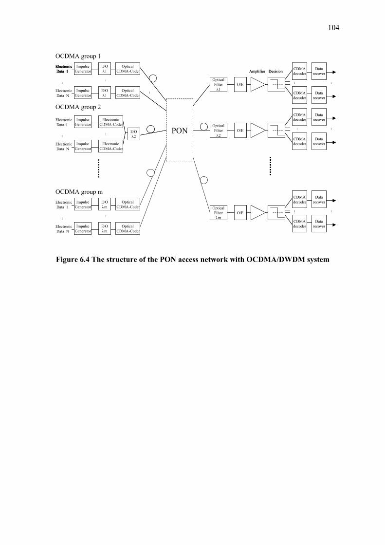
104
Electronic Data 1
E/O Optical CDMA-Coder
ImpulseGenerator
PON
CDMAdecoder
DatarecoverDesision
CDMAdecoder
Datarecover
Amplifier
OpticalFilterλ1
Electronic Data 1
E/Oλ1
Optical CDMA-Coder
ImpulseGenerator
E/Oλ1
Optical CDMA-Coder
ImpulseGenerator
O/E
Electronic Data 1
E/Oλ2
ImpulseGenerator
Electronic CDMA-Coder
ImpulseGenerator
Electronic CDMA-Coder
ImpulseGenerator
Electronic Data N
CDMAdecoder
Datarecover
CDMAdecoder
Datarecover
OpticalFilterλ2
O/E
CDMAdecoder
Datarecover
CDMAdecoder
Datarecover
OpticalFilterλn
O/E
Electronic Data 1
E/O Optical CDMA-Coder
ImpulseGenerator
E/Oλn
Optical CDMA-Coder
ImpulseGenerator
E/Oλn
Optical CDMA-Coder
ImpulseGenerator
Electronic Data N
Electronic Data 1
E/O Optical CDMA-Coder
ImpulseGenerator
PON
CDMAdecoder
DatarecoverDesision
CDMAdecoder
Datarecover
Amplifier
OpticalFilterλ1
Electronic Data 1
E/Oλ1
Optical CDMA-Coder
ImpulseGenerator
E/Oλ1
Optical CDMA-Coder
ImpulseGenerator
Electronic Data N
O/E
E/Oλ2
ImpulseGenerator
Electronic CDMA-Coder
ImpulseGenerator
Electronic CDMA-Coder
ImpulseGenerator
CDMAdecoder
Datarecover
CDMAdecoder
Datarecover
OpticalFilterλ2
O/E
CDMAdecoder
Datarecover
CDMAdecoder
Datarecover
OpticalFilterλm
O/E
E/O Optical CDMA-Coder
ImpulseGenerator
E/Oλm
Optical CDMA-Coder
ImpulseGenerator
E/Oλm
Optical CDMA-Coder
ImpulseGenerator
OCDMA group 1
OCDMA group 2
OCDMA group m
Figure 6.4 The structure of the PON access network with OCDMA/DWDM system
105
Chapter 7 Conclusions
Though the technology of CDMA has been already successfully used in wireless data
transmission, OCDMA remains outside the mainstream of the research in optical
communications. However, with the progress in the optical network technology and the
increasing demand for simple access protocol, the research on OCDMA has become active
recently, and it would be a potential candidate technology for future optical networks,
especially for optical access networks. In this thesis, we present the results of our research in
the field of OCDMA communications. Our intention is to explore the possibility of an
OCDMA system using electronic en/decoding and the possibility of its combination with
DWDM. Therefore, using the narrow spectral optical sources ready for insertion into a
DWDM channel, we implemented the OCDMA demonstration system for the comparison of
electronic and optical en/decoding.
We have evaluated the current experimental research in the OCDMA field, the criteria include
the achieved number of access users, the requirement of spectral width, feasibility for a
practical system, etc.. The results show that none of the contemporary real OCDMA systems
can demonstrate the primary advantages of OCDMA technology, such as a large access
number.
We observed the influence of the interferometric noise produced by overlapping light waves
from the same optical source during optical encoding and decoding. The noise produced at the
optical encoder could be reduced to an acceptable level by increasing the extinction ratio of
the output of the electronic/optical converter. But at the optical decoder all chips within a
designed codeword have to be overlaid to despread the signal. By analyzing the optical
encoding and decoding processes, we concluded that in an OCDMA system the
interferometric noise is one of the main sources for system limitation. With a coherent optical
decoder, the interferometric noise can be avoided, as long as complete coherent decoding is
achieved. In an optical decoder the arriving phase of each chip is very sensitive to the small
wander of temperature, thus the temperatures of en/decoders have to be controlled.
Furthermore, from the tiny variance of temperature (<10 ) remaining under the C°−5
106
temperature controlling, it could produce big phase drifting and strong noise. Then a servo-
control for phase drift tracking has to be set for each branch within the decoder. Furthermore,
when code weight is larger than two, the information about the phase in each branch cannot
be recovered from the received signal. We conclude that without a great technical
breakthrough, the OCDM technology uniquely using optical en/decoding processes cannot
compete with gradually matured DWDM in the near future.
Using electronic encoding and decoding in an OCDMA system could avoid the above
mentioned interferometric noise. We have examined the performance of OCDMA systems
with an electronic en/decoding process through the implementation of a demonstration system
with three users, each operating with a data rate up to 155Mbit/s. With the improvement of
clock frequency of electronic components in the future, the scheme with electronic coding for
higher chip rates up to 10Gchips/s, even 40Gchips/s could be possible. In addition, a logic
electronic decoder has the function of the hard-limiter, therefore the BER will be reduced. To
my best knowledge we are the first to give an algorithm for exact calculation of the BER of
the OCDMA system with a hard limiter.
Based on the implemented demonstration system, we have analyzed the possibilities of an
access scheme combining OCDMA and DWDM. When the differences between the center
frequencies of the optical sources of an OCDMA group are bigger than the bandwidth of the
chips, and all spectrum used by OCDMA group is within a DWDM channel, the noise
performance will be good enough to achieve the transmission. The combination of OCDMA
and DWDM might find its market in access networks, due to larger access number and higher
flexibility of the network architecture. The results of our work on the application of OCDMA
over DWDM show that this scheme by using matured technology can be adapted to the
requirements imposed by the access network.
107
Appendix
Appendix A1 An Algorithm of BER with Hard-limiter
Here we give an algorithm of the BER in OCDMA system with hard-limiter at the receiver.
An optical hard limiter converts the channel from an “adder channel” to a “binary OR-
channel” by removing intensity information from the fiber beyond the two levels of “off” and
“on”. In contrast to the published algorithm in [22, 23, 28], which only gives an upper bound
limit, we give a exact calculation of BER with hard-limiter, that is suitable for simulation with
computer programs.
We will model the network as chip synchronous, and T will be the unit of time shift. In
other word, T (the time duration of one bit of information) is divided into segments, i.e.,
. Here we assume that the codeword is , i.e. only one chip overlap
for the auto- and cross-correlation, and N users are addressable by the code family. The a
priori probability of Mark and Null for all users is represented as and . We define
as the probability of corresponding values i and j, in which i is the number of all the other
users except a desired user in the system and j is the number of positions, which locate in the
codeword of the desired user and are disturbed by chip of the others users, and, from
its definition. i means that there are two or more disturbances in the same chip positions
within w. The hard-limiter can limit the signal amplitude with the result that the disturbed
value at one position is only 1, i.e. after hard-limiter, only when all of the w positions are
disturbed, there is a possible bit error.
C
,, w
D CL
P
CCD TLT ⋅=
jiP ,
)1,1(LC
MarkP Null
wj ≤
j>
When only two users are in the system, i.e. i=1,
⋅
−=
−= q
wLwP
wP
CMark 1
11
10,1 (A1.1)
qw
LwP
wP
CMark ⋅
=
=
111,1 (A1.2)
108
where is the probability of the other user, MarkPCL
w is the probability of the disturbance when
one of the w chips of other user is located in one position within desired codeword, and
is the number of the empty position within the codeword. We define
1w
CMark L
wPq ⋅= , in order
to simplify the expressions.
When another user is added to the system, 2=i , based on the above analysis, there are three
cases: all w positions of the desired codeword are empty, ; only one position is disturbed,
; and two positions are disturbed, . They can be represent by
0,2P
1,2P 2,2P
⋅
−⋅= q
wPP
110,10,2 (A1.3)
⋅
−−+⋅
⋅= q
wPq
wPP
11
11 1,10,11,2 (A1.4)
qw
PP ⋅
−=
11
1,12,2 (A1.5)
where means w-1 empty positions in the desired codeword could be disturbed. Now
there are one or two positions of w disturbed and when , there is no bit error.
−1
1w
3≥w
When one more user is added to the system, 3=i ,
⋅
−⋅= q
wPP
110,20,3 (A1.6)
⋅
−−+⋅
⋅= q
wPq
wPP
11
11 1,20,21,3 (A1.7)
⋅
−−+⋅
−⋅= q
wPq
wPP
12
11
12,21,22,3 (A1.8)
qw
PP ⋅
−=
12
2,23,3 (A1.9)
In general, when i , w<
109
⋅
−⋅= − q
wPP ii 1
10,10, (A1.10)
⋅
−−+⋅
⋅= −− q
wPq
wPP iii 1
11
1 1,10,11, (A1.11)
⋅
−−+⋅
−⋅= −− q
wPq
wPP iii 1
21
11
2,11,12, (A1.12)
... ...
ikqkw
Pqkw
PP kikiki <<
⋅
−−+⋅
−−⋅= −−− 2
11
1)1(
,11,1, (A1.13)
......
qiw
PP iiii ⋅
−−= −− 1
)1(1,1, (A1.14)
When i w=
⋅
−⋅= − q
wPP ww 1
10,10, (A1.15)
⋅
−−+⋅
⋅= −− q
wPq
wPP iww 1
11
1 1,10,11, (A1.16)
... ...
wkqkw
Pqkw
PP kwkwkw <<
⋅
−−+⋅
−−⋅= −−− 1
11
1)1(
,11,1, (A1.17)
......
qPP wwww ⋅
= −− 1
11,1, (A1.18)
wwNull PP ,⋅ is the probability of a bit error with w other users. means that when desired
user transmits Null, bit error emerges.
NullP
When 1−<< Niw
⋅
−⋅= − q
wPP ii 1
10,10, (A1.20)
110
⋅
−−+⋅
⋅= −− q
wPq
wPP iii 1
11
1 1,10,11, (A1.21)
⋅
−−+⋅
−⋅= −− q
wPq
wPP iii 1
21
11
2,11,12, (A1.22)
... ...
wkqkw
Pqkw
PP kikiki <<
⋅
−−+⋅
−−⋅= −−− 2
11
1)1(
,11,1, (A1.23)
......
wiwiwi PqPP ,11,1, 11
−−− +⋅
= (A1.25)
wiNull PP ,⋅ is the probability of the bit error with i+1 other users. Here, because is the
probability for the case of emerging bit error, the new other user doesn’t play any roll in this
case, so it is directly added in .
wiP ,1−
wiP ,
At last when , 1−= Ni
... ...
wNwNwN PqPP ,21,2,1 11
−−−− +⋅
= (A1.26)
wNNull PP ,1−⋅ is the exact BER of the decoder with hard-limiter.
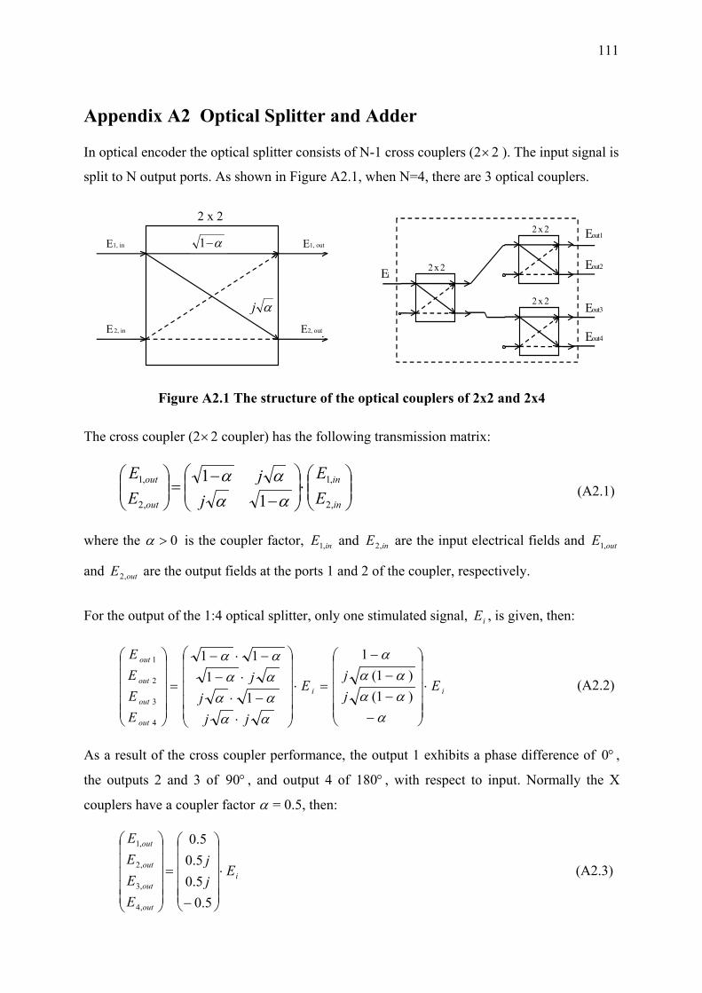
111
Appendix A2 Optical Splitter and Adder
In optical encoder the optical splitter consists of N-1 cross couplers (2×2 ). The input signal is
split to N output ports. As shown in Figure A2.1, when N=4, there are 3 optical couplers.
E1, in
E 2, in E2, out
E1, outα−1
αj
2 x 2
Ei
Eout1
Eout2
Eout3
Eout4
2 x 2
2 x 2
2 x 2
Figure A2.1 The structure of the optical couplers of 2x2 and 2x4
The cross coupler (2×2 coupler) has the following transmission matrix:
⋅
−−
=
in
in
out
out
EE
jj
EE
,2
,1
,2
,1
11
αααα
(A2.1)
where the 0>α is the coupler factor, and are the input electrical fields and
and are the output fields at the ports 1 and 2 of the coupler, respectively.
inE ,1 inE ,2 outE ,1
outE ,2
For the output of the 1:4 optical splitter, only one stimulated signal, , is given, then: iE
ii
out
out
out
out
Ejj
E
jjj
j
EEEE
⋅
−−−
−
=⋅
⋅−⋅
⋅−−⋅−
=
ααααα
α
αααααααα
)1()1(
1
11
11
4
3
2
1
(A2.2)
As a result of the cross coupler performance, the output 1 exhibits a phase difference of ,
the outputs 2 and 3 of 90 , and output 4 of 180 , with respect to input. Normally the X
couplers have a coupler factor
°0
° °
α = 0.5, then:
i
out
out
out
out
Ejj
EEEE
⋅
−
=
5.05.05.05.0
,4
,3
,2
,1
(A2.3)
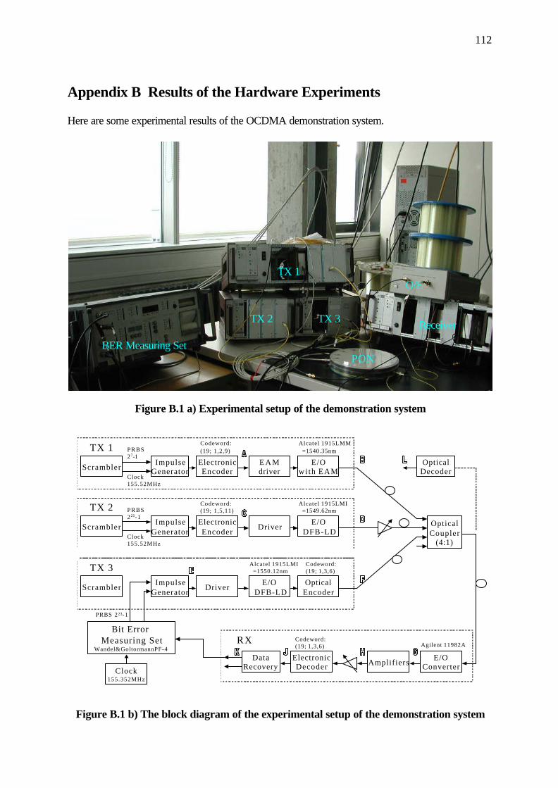
112
Appendix B Results of the Hardware Experiments
Here are some experimental results of the OCDMA demonstration system.
W
T
Scr
T
Scr
T
Scr
Figu
3 2
1
E
BER Measuring Set
Figure B.1 a) Experimental setup of th
Bit Error Measuring Setandel&GoltormannPF-4
PRBS27-1
Clock155.52MHz
PRBS 223-1
X 1Impulse
Generator
Codeword:(19; 1,2,9)
Alca=15
ElectronicEncoder
E A Mdriver wi tambler
PRBS221-1
Clock155.52MHz
X 2Impulse
Generator
Codeword:(19; 1,5,11)
Alca=15
ElectronicEncoder
Driver DF
ambler
X 3Impulse
Generator
Co(1
OEn
DriverE/O
DFB-LDambler
Alcatel 1915LMI=1550.12nm
Clock155.352MHz
RX
DataRecovery
Codew(19; 1
ElectDeco
re B.1 b) The block diagram of the experiment
TX
TXTX
e demonstration syste
tel 1915LMM40.35nm
E/Oh EAM
tel 1915LMI49.62nm
E/OB-LD
deword:9; 1,3,6)
pticalcoder
ord:,3,6)
ronicder Amplifiers
al setup of the demon
Receiver
O/
PON
m
OpticalCoupler
(4:1)
E/OConverter
Agilent 11982A
OpticalDecoder
stration system
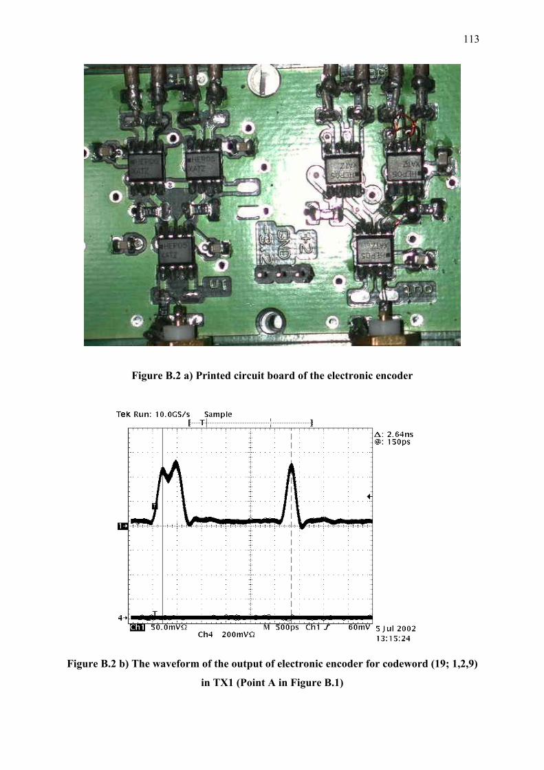
113
Figure B.2 a) Printed circuit board of the electronic encoder
Figure B.2 b) The waveform of the output of electronic encoder for codeword (19; 1,2,9)
in TX1 (Point A in Figure B.1)
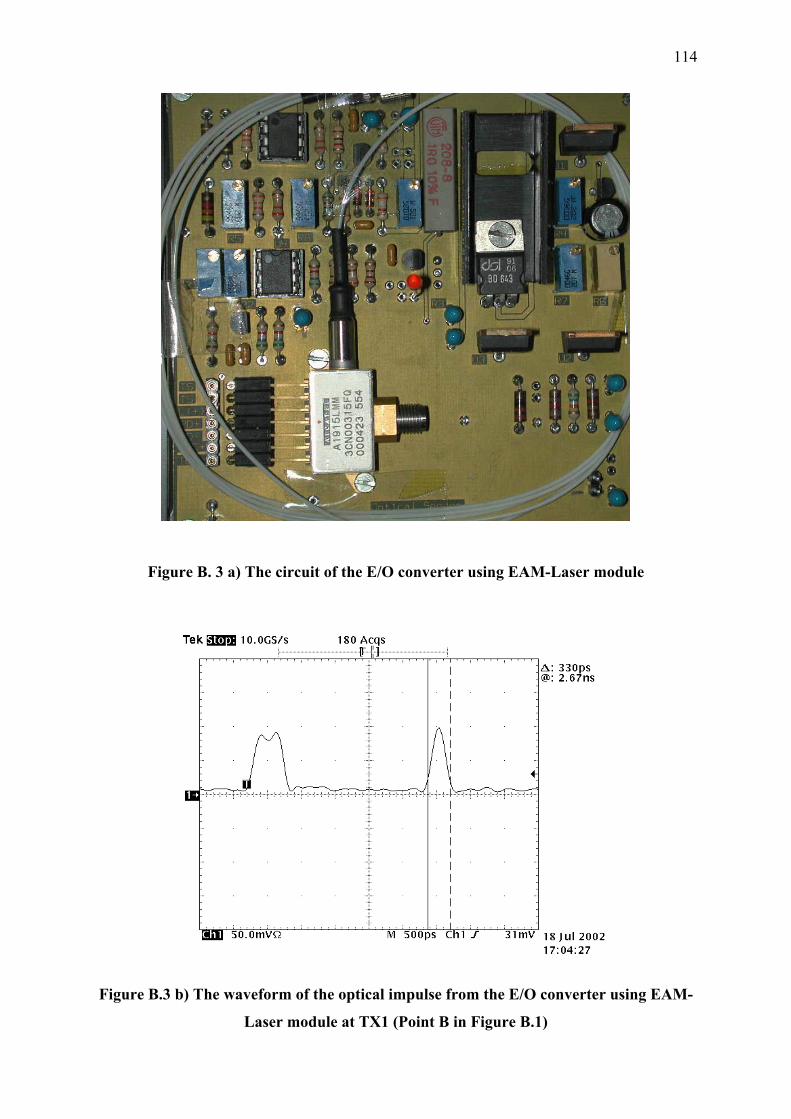
114
Figure B. 3 a) The circuit of the E/O converter using EAM-Laser module
Figure B.3 b) The waveform of the optical impulse from the E/O converter using EAM-
Laser module at TX1 (Point B in Figure B.1)
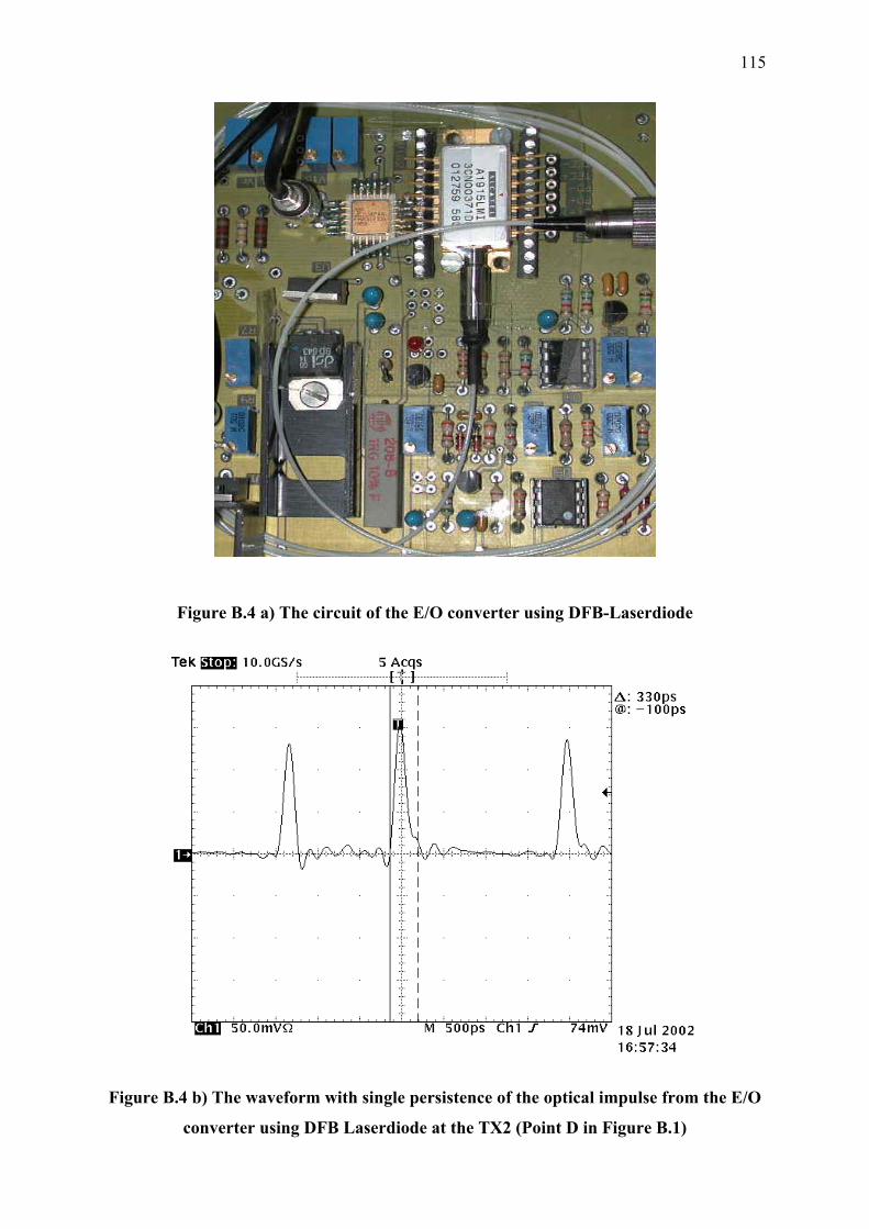
115
Figure B.4 a) The circuit of the E/O converter using DFB-Laserdiode
Figure B.4 b) The waveform with single persistence of the optical impulse from the E/O
converter using DFB Laserdiode at the TX2 (Point D in Figure B.1)
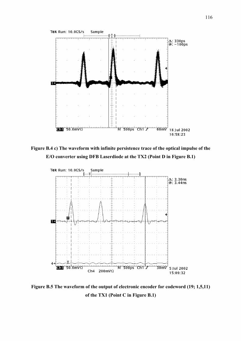
116
Figure B.4 c) The waveform with infinite persistence trace of the optical impulse of the
E/O converter using DFB Laserdiode at the TX2 (Point D in Figure B.1)
Figure B.5 The waveform of the output of electronic encoder for codeword (19; 1,5,11)
of the TX1 (Point C in Figure B.1)
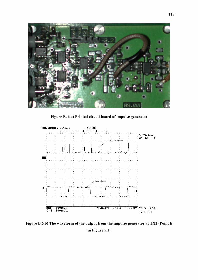
117
Figure B. 6 a) Printed circuit board of impulse generator
Figure B.6 b) The waveform of the output from the impulse generator at TX2 (Point E
in Figure 5.1)
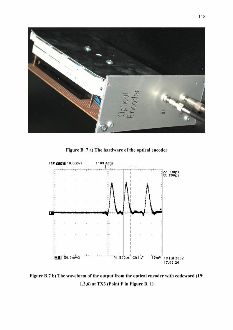
118
Figure B. 7 a) The hardware of the optical encoder
Figure B.7 b) The waveform of the output from the optical encoder with codeword (19;
1,3,6) at TX3 (Point F in Figure B. 1)
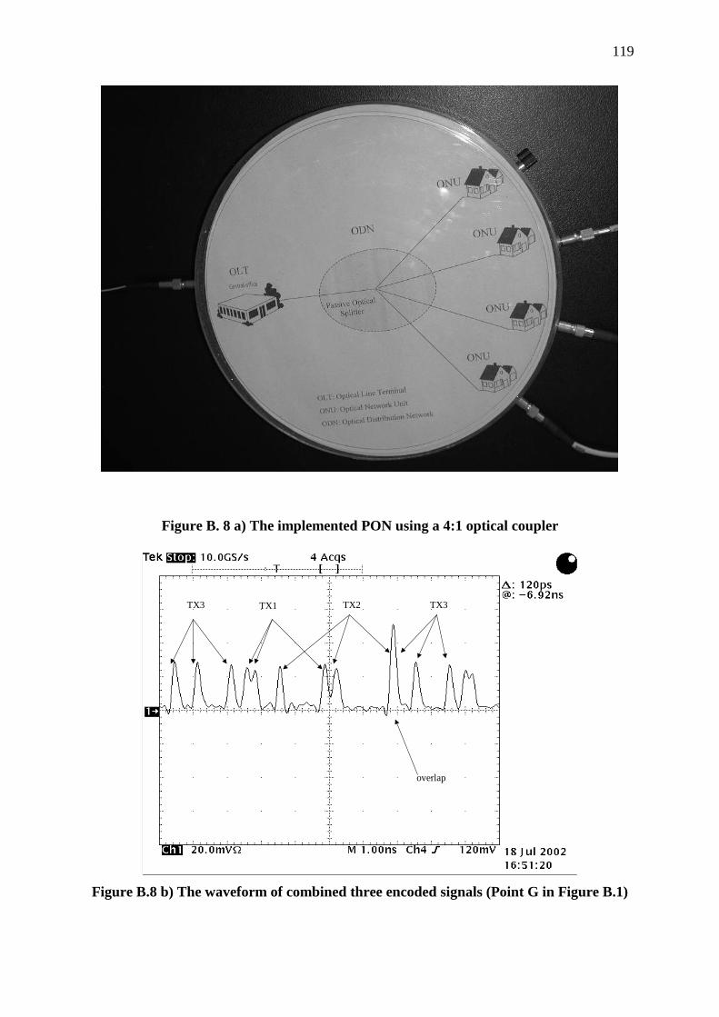
119
Figure B. 8 a) The implemented PON using a 4:1 optical coupler
TX3 TX1 TX2 TX3
overlap
Figure B.8 b) The waveform of combined three encoded signals (Point G in Figure B.1)
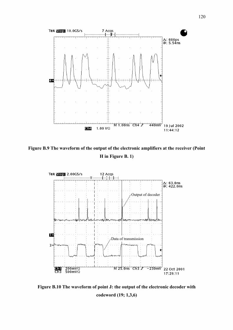
120
Figure B.9 The waveform of the output of the electronic amplifiers at the receiver (Point
H in Figure B. 1)
Output of decoder
Data of transmission
Figure B.10 The waveform of point J: the output of the electronic decoder with
codeword (19; 1,3,6)
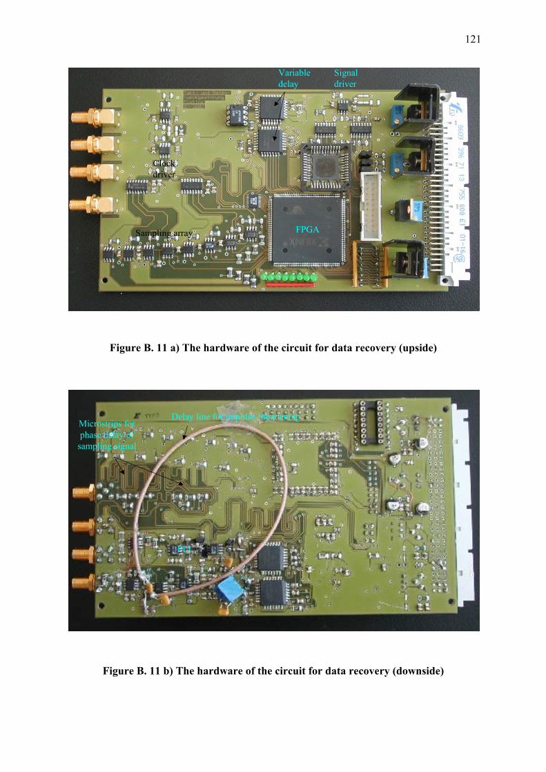
121
Variabledelay
Signaldriver
FPGASampling array
Clockdriver
Figure B. 11 a) The hardware of the circuit for data recovery (upside)
Delay line for impulse-broadeningMicrostrips forphase delay of
sampling signal
PLL
Figure B. 11 b) The hardware of the circuit for data recovery (downside)
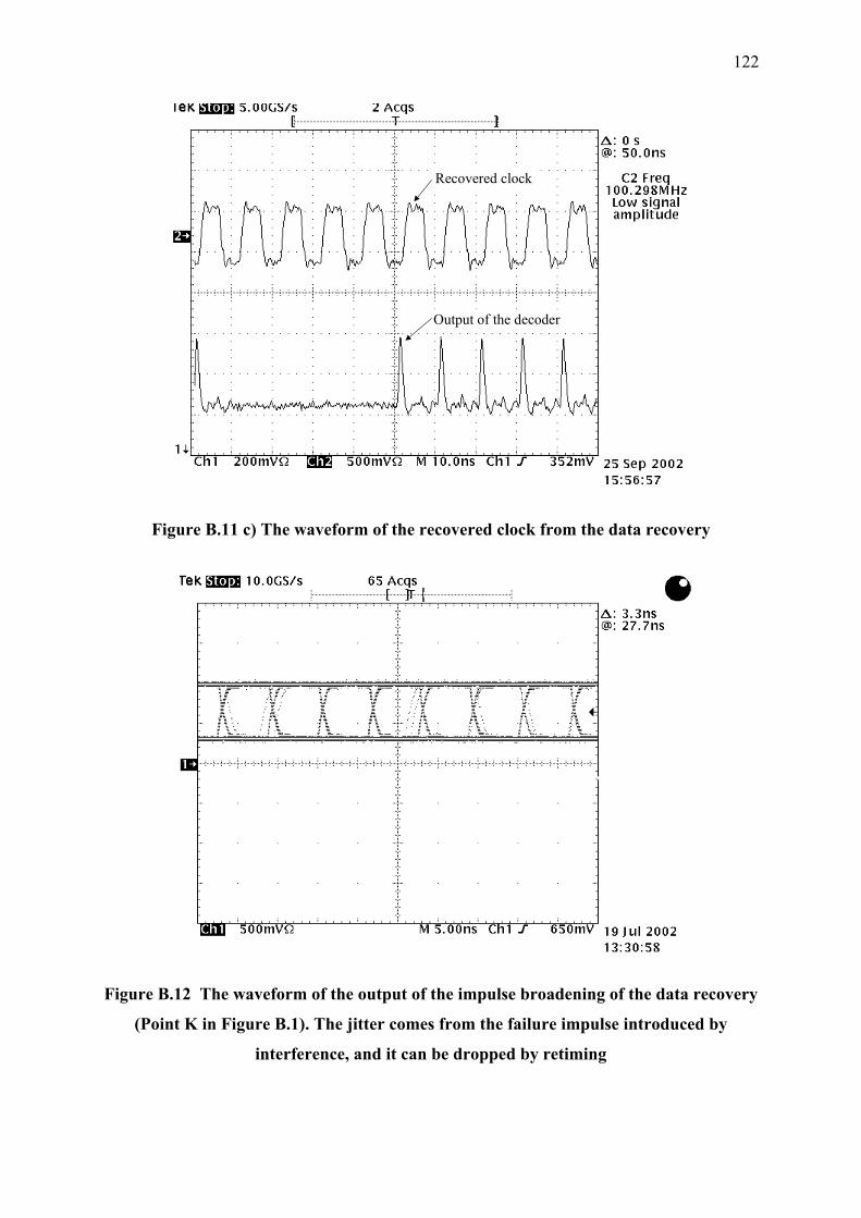
122
Recovered clock
Output of the decoder
Figure B.11 c) The waveform of the recovered clock from the data recovery
Figure B.12 The waveform of the output of the impulse broadening of the data recovery
(Point K in Figure B.1). The jitter comes from the failure impulse introduced by
interference, and it can be dropped by retiming
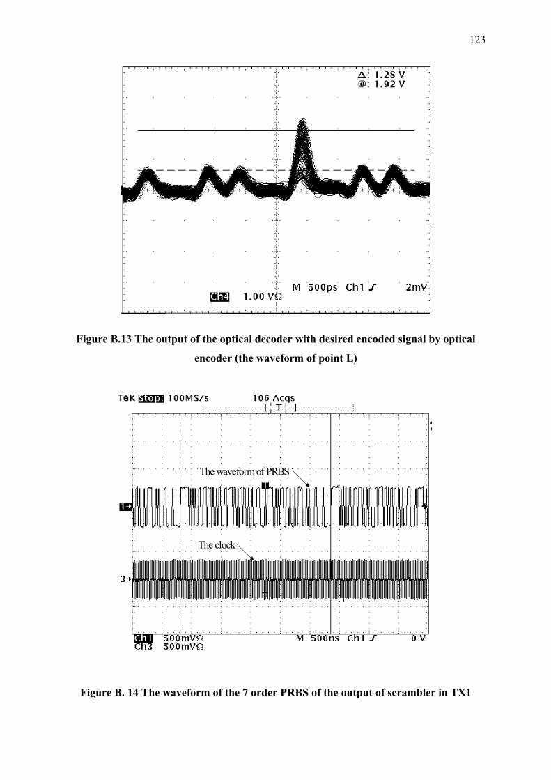
123
Figure B.13 The output of the optical decoder with desired encoded signal by optical
encoder (the waveform of point L)
The waveform of PRBS
The clock
Figure B. 14 The waveform of the 7 order PRBS of the output of scrambler in TX1
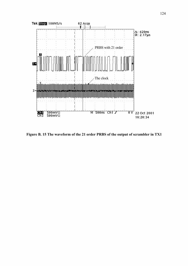
124
PRBS with 21 order
The clock
Figure B. 15 The waveform of the 21 order PRBS of the output of scrambler in TX1
125
Bibliography
[1] J. Speidel, “Zugangsnetze im Wettbewerb,” Hüthig-Verlag, Heidelberg, 2000.
[2] M. Medard and S. Lumetta, “Architectural Issues for Robust Optical Access,” IEEE
Communications Magazine, July 2001.
[3] R. Prasad, et al., “An Overview of CDMA Evolution Towards Wideband CDMA,” IEEE
Communication Surveys, Vol. 1, No. 1, 1998.
[4] D. D. Sampson, G. J. Pendock and R. A. Griffin, “Photonic Code-Division Multiple-
Access Communications,” Fiber and Integrated Optics, Vol. 16, PP. 129-157, 1997.
[5] Technical Progress Report, “Broadband Wireless Standards,” Institute for
Telecommunication Sciences of National Telecommunications and Information
Administration (NTIA) of the U.S., 2000.
[6] P. Prucnal, M. Santoro and T. Fan, “Spread Spectrum Fiber-Optical Local Area Network
Using Optical Processing,” IEEE Journal of Lightwave Technology, Vol. 4, No. 5, 1986.
[7] J. A. Salehi, “Emerging Optical Code-Division Multiple Access Communications
System,” IEEE Network, March 1989.
[8] D. Buchholz, “Broadband Fiber Access: A Fiber-to-the-Customer Access Architecture,”
Bell Labs Technical Journal, January-March 1999.
[9] F. Khaleghi and M. Kavehred, “A Subcarrier Multiplexed CDM Optical Local Area
Network, Theory and Experiment,” IEEE Transactions on Communications, Vol. 43,
No.1, 1995.
[10] J. A. Salehi, A. Weiner and J. P. Heritage, “Coherent Ultrashort Light Pulse CDMA
Communications Systems,” IEEE Journal of Lightwave Technology, Vol. 8, No. 3,
1990.
[11] K. Iversen, D. Hampicke and F. Schleuß, “Optischer CDMA: Systeme und Sequenzen,”
Nachrichtentech., Elektron., SCIENCE, Berlin 45 (1995) 5.
[12] A. J. Viterbi, “CDMA: Principles of Spread Spectrum Communication,” Reading, Mass
Addison-Wesley, ISBN 0-201-63374-4, 1995.
[13] H. Kim and Y. C. Chung, “Passive Optical Network for CDMA-Based Microcellular
Communications Systems,” IEEE Journal of Lightwave Technology, Vol. 19, No. 3,
2001.
126
[14] Robert Fritsch, “3. Ergebnisbericht zum FMS-Projekt III. 3. Arbeitsbereich: Optisches
CDMA als Mehrfachzugriffsverfahren für Rückkanäle in optischen Verteilnetzen im
Teilnehmerzuangsbereich,” Institut für Nachrichtenübertragung, Universität Stuttgart,
Dezember 1999, http://www.inue.uni-stuttgart.de/FMS/abschluss.
[15] Roman Dischler, “1. Ergebnisbericht zum FMS-Projekt III. 3. Arbeitsbereich: Optisches
CDMA als Mehrfachzugriffsverfahren für Rückkanäle in optischen Verteilnetzen im
Teilnehmerzugangsbereich,” Institut für Nachrichtenübertragung, Universität Stuttgart,
31. März 1998, http://www.inue.uni-stuttgart.de/FMS/abschluss.
[16] F. Chung, J. A. Salehi and V. Wie, “Optical Orthogonal Codes: Design, Analysis and
Application,” IEEE Transactions on Information Theory, Vol. 35, No. 3, 1989.
[17] V. Svetislav, Z. Kostic and E. Tiltebaum, “A New Family of Optical Code Sequences
for Use in Spread-Spectrum Fiber-Optical Local Area Networks,” IEEE Transactions on
Communications, Vol. 41, No. 8, 1993.
[18] Z. Wie, et al., “Modified Quadratic Congruence Codes for Fiber Bragg-Grating-Based
Spectral Amplitude Coding Optical CDMA Systems,” IEEE Journal of Lightwave
Technology, Vol. 19, No. 9, 2001.
[19] A. S. Holmes and R. A. Syms, “All-Optical CDMA Using ‘Quasi-Prime’ Codes,” IEEE
Journal of Lightwave Technology, Vol. 10, No. 2, 1992.
[20] S. Tamura and S. Nakano, “Optical Code-Multiplex Transmission by Gold Sequences,”
IEEE Journal of Lightwave Technology, Vol. 3, No. 1, 1985.
[21] L. Tancevski and I. Adonovic, “Block Multiplexing Codes for Optical Ladder Network
Correlators,” IEEE Photonics Technology Letters, Vol. 6, No. 2, 1994.
[22] J. A. Salehi, “Code Division Multiple-Access Techniques in Optical Fiber Networks -
Part I: Fundamental Principles,” IEEE Transactions on Communications, Vol. 37, No. 8,
1989.
[23] J. A. Salehi and C. A. Brackett, “Code Division Multiple Access Techniques in Optical
Fiber Networks - Part 2: Systems Performance Analysis,” IEEE Transactions on
Communications, Vol. 37, No. 8, 1989.
[24] M. Azizoglu, J. A. Salehi and Y. Li, “Optical CDMA via Temporal Codes,” IEEE
Transactions on Communications, Vol. 40, No.7, 1992.
[25] L. Tancevski, et al., “Massive Optical LAN’s Using Wavelength Hopping/Time
Spreading with Increased Security.” IEEE Photonics Technology Letters, Vol. 8, No. 7,
1996.
127
[26] T. W. Mossberg and M. G. Raymer, “Optical Code-Division Multiplexing: The
Intelligent Optical Solution,” Optics&Photonics News, March 2001.
[27] G. Pendock and D. Sampson, “Capacity of Coherence Multiplexed CDMA Networks,”
Conference on Lasers and Electrooptics (CLEO’96), Anaheim, 1996.
[28] T. Ohtsuki, “Performance Analysis of Direct-Detection Optical Asynchronous CDMA
Systems with Double Optical Hard-Limiters”, IEEE Journal of Lightwave Technology,
Vol. 15, No. 3, 1997.
[29] G. Foschini and G. Vannucci, “Using Spread-Spectrum in a High-Capacity Fiber-
Optical Local Network,” IEEE Journal of Lightwave Technology, Vol. 6, No. 3, 1988.
[30] E. Shivaleela, K. Sivarajan and A. Selvarajan, “Design of a New Family of Two-
Dimensional Codes for Fiber-Optic CDMA Networks,” IEEE Journal of Lightwave
Technology, Vol. 16, No. 4, 1998.
[31] M. Kavehrad and D. Zaccarin, “Optical Code-Division-Multiplexed System Based on
Spectral Encoding of Noncoherent Sources,” IEEE Journal of Lightwave Technology,
Vol. 13, No. 3, 1995.
[32] L. Tanceveski and I. Andonovic, “Hybrid Wavelength Hopping/Time Spreading
Schemes for Use in Massive Optical Networks with Increased Security,” IEEE Journal
of Lightwave Technology, Vol. 14, No. 12, 1996.
[33] S. Yegnanarayanan and A. S. Bhushan, “Fast Wavelength-Hopping Time-Spreading
Encoding/Decoding for Optical CDMA,” IEEE Photonics Technology Letters, Vol. 12,
No. 5, 2000.
[34] N. Wada, H. Sotobayashi and K. Kitayama, “2.5Gbit/s Time-Spread/Wavelength-Hop
Optical Code Division Multiplexing Using Fiber Bragg Grating with Supercontinuum
Light Source,” IEE Electronics Letters, Vol. 36, No. 9, 2000.
[35] H. Fathallah, L. A. Rusch, et al., “Passive Optical Fast Frequency-Hop CDMA
Communications System,” IEEE Journal of Lightwave Technology, Vol. 17, No. 3,
1999.
[36] H. B. Jaafar, S. LaRochelle and P. Y. Cortes, “1.25Gbit/s Transmission of Optical FFH-
OCDMA Signals over 80Km with 16 Users,” Optical Fiber Communications
Conference and Exhibition, 2001.
[37] R. A. Griffin, D. D. Sampson and D. A. Jackson, “Demonstration of Data Transmission
Using Coherent Correlation to Reconstruct a Coded Pulse Sequence,” IEEE, Photonics
Technology Letters, Vol. 4, No. 5, 1992.
128
[38] Y. L. Chang and M. E. Marhic, “Fiber-Optic Ladder Networks for Inverse Decoding
Coherent CDMA,” IEEE Journal of Lightwave Technology, Vol. 10, No. 12, 1992.
[39] H. P. Sardesai, C.-C. Chang and A. M. Weiner, “A Femtosecond Code-Division
Multiple-Access Communications System Test Bed,” IEEE Journal of Lightwave
Technology, Vol. 16, No. 11, 1998.
[40] P. C. Teh, M. Ibsen, et al., “Demonstration of a Four-Channel WDM/OCDMA System
Using 255-Chip 320-Gchip/s Quarternary Phase Coding Gratings,” IEEE, Photonics
Technology Letters, Vol. 14, No. 2, 2002.
[41] P. C. Teh, M. Ibsen, et al., “A 16-Channel OCDMA System (4 OCDMA x 4 WDM)
Based on 16 Chip, 20Gchip/s Superstructure Fiber Bragg Gratings and DFB Fiber Laser
Transmitters” OCIS codes: 060.4250, 2002.
[42] N. Wada and W. Chujo, “160Gbit/s OCDMA/WDM (10Gbit/s x 4CDMA x 4WDM)
Transmission with a Novel Side-Lobes Suppression Detection,” Optical Fibre
Communication Conference, Anaheim, 2001.
[43] H. Sotobayashi and W. Chujo, “1.6Bit/s/Hz, 6.4Tbit/s OCDM/WDM (4 OCDM x 40
WDM x 40 Gbit/s) Transmission Experiment,” ECOC, 2001.
[44] T. Pfeiffer, J. Kissing, et al., “Coarse WDM/CDM/TDM Concept for Optical Packet
Transmission in Metropolitan and Access Networks Supporting 400 Channels at
2.5Gbit/s Peak Rate,” IEEE Journal of Lightwave Technology, Vol. 18, No. 12, 2000.
[45] T. Pfeiffer, B. Deppisch, et al., “Optical CDMA Transmission for Robust Realization of
Complex and Flexible Multiple Access Networks,” Optical Fibre Communication
Conference, Paper WM-51, 1999.
[46] T. Pfeiffer, B. Deppisch, et al., “High Speed Optical Network For Asynchronous Multi-
user Access Applying Periodic Spectral Coding of Broadband Sources,” IEEE
Electronics Letters, Vol. 33, No. 25, 1997.
[47] T. Pfeiffer, B. Deppisch, et al., “Temperature in Sensitive Spectrally Encoded Optical
Multichannel System for Simultaneous Transmission of Digital Baseband and Subcarrier
signals,” IEEE Electronics Letters, Vol. 36, No. 5, 2000.
[48] J. A. Salehi and C. A. Brackett, “Fundamental Principles of Fiber Optics Code Division
Multiple Access (FO-CDMA),” IEEE International Conference On Communications,
June 1987.
[49] G. J. Pendock and D. D. Sampson, “Increasing the Transmission Capacity of Coherence
Multiplexed Communication Systems by Using Differential Detection,” IEEE Photonics
Technology Letters, Vol. 7, No. 12, 1995.
129
[50] G. Vannucci and K. Kikuchi. “Experimental Spreading and Despreading of the Optical
Spectrum,” IEEE Transactions on Communications, Vol. 37, No. 7, 1989.
[51] N. Wada and K. Kitayama, “Fundamental Properties of 10Gbit/s Coherent Optical Code
Division Multiplexing: Experiment,” Optical Review (Japan), Vol. 5, No. 1, 1998.
[52] H. Sotobayashi, W. Chujo and K. Kitayama, “3 x 10Gbit/s OCDM Transmission at
1550nm Band over 150km Standard Fiber Using Midspan Optical Phase Conjugation,”
OECC2000, 14A2-4, pp. 456-457, 2000.
[53] M. Razavi and J. A. Salehi, “Statistical Analysis of Fiber-Optical CDMA
Communication Systems – Part I: Device Modeling,” IEEE Journal of Lightwave
Technology, Vol. 20, No. 8, 2002.
[54] M. Razavi and J. A. Salehi, “Statistical Analysis of Fiber-optical CDMA
Communication Systems – Part II: Incorporating multiple optical amplifiers,” IEEE
Journal of Lightwave Technology, Vol. 20, No. 8, 2002.
[55] PTDS product information, www.virtualphotionics.com.
[56] F. Forghieri, R. W. Tkach and A. R. Chraplyvy, “Fibre Nonlinearities and Their Impact
on Transmission Systems: In Optical Fibre Telecommunications,” Vol. IIIa, Academic
Press, 1997.
[57] S. Shen and A. M. Weiner, “Suppression of WDM Interference for Error-Free Detection
of Ultrashort-Pulse CDMA Signals in Spectrally Overlaid Hybrid WDM-CDMA
Operation,” IEEE Photonics Technology Letters, Vol. 13, No. 1, 2001.
[58] J. Chen and G. Yang, “CDMA Fiber-Optic Systems with Optical Hard Limiters,” IEEE
Journal of Lightwave Technology, Vol. 19, No. 7, 2001.
[59] M. Pauer, P. J. Winzer and W. R. Leeb, “Bit Error Probability Reduction in Direct
Detection Optical Receivers Using RZ Coding,” IEEE Journal of Lightwave
Technology, Vol. 19, No. 9, 2001.
[60] P. Winzer and A. Kalmar, “Sensitivity Enhancement of Optical Receivers by Impulsive
Coding,” IEEE Journal of Lightwave Technology, Vol. 17, No. 2, 1999.
[61] S. Kim, J. Lee and J. Jeong, “Transmission Performance of 10-Gbit/s Optical Duobinary
Transmission Systems Considering Adjustable Chirp of Nonideal LiNbO3 Mach-
Zehnder Modulators Due to Applied Voltage Ratio and Filter Bandwidth,” IEEE Journal
of Lightwave Technology, Vol. 19, No. 4, 2001.
[62] H. Sunnerud, “Polarization-Mode Dispersion in Optical Fibers: Characterization,
Transmission Impairments and Compensation,” Technical Report No. 399, Photonics
Laboratory, Chalmers University of Technology, Göteborg, March 2001.
130
[63] J. Hansryd, H. Sunnerud, et al., “Impact of PMD on Four-Wave-Mixing-Induced
Crosstalk in WDM Systems,” IEEE Photonics Technology Letters Vol. 12, No. 9, 2000.
[64] K. Petermann, “Laser Diode Modulation and Noise,” New York, Kluwer-Academic,
1993.
[65] P. J. Legg, M. Tur and I. Andonovic, “Solution Paths to Limit Interferometric Noise
Induced Performance Degradation in ASK/Direct Detection Lightwave Networks,”
IEEE Journal of Lightwave Technology, Vol. 14, No. 9, 1996.
[66] A. C. Kersey, A. Dandridge and A. B. Tevten, “Dependence of Visibility on Input
Polarization in Interferometric Fiber-Optic Sensors,” Optical Letters, Vol. 13, pp. 288-
290, 1988.
[67] I. H. Malitson, “Interspecimen Comparison of the Refractive Index of Fused Silica,”
Journal of Optical Society American, Vol. 55, pp. 1205-1209, 1965.
[68] M. R. Dale and R. M. Gagliardi, “Channel Coding for Asynchronous Fiberoptic CDMA
Communications,” IEEE Transactions on Communications, Vol. 43, No. 9, 1995.
[69] J. Zhang, et al., “Interferometric Noise in Optical Time Division Multiplexing
Transmission System,” IEEE Journal of Lightwave Technology, Vol. 20, No. 8, 2002.
[70] G. Clark and J. Cain, “Error-Correction Coding for Digital Communications,” New
York, Plenuim, March 1988.
[71] VPI transmission Maker™- VPI component Maker™, “Photonic Modules Reference
Manual.”
[72] R. H. Wentworth, “Theoretical Noise Performance of Coherence-Multiplexed
Interferometric Sensors,” IEEE Journal of Lightwave Technology, Vol. 7, No. 6, 1989.
[73] R. W. Tkach and A. R. Chraplyvy, “Phase Noise and Linewidth in an InGaAsP DFB
Laser,” IEEE Journal of Lightwave Technology, Vol. 4, No. 11, 1986.
[74] M. Gustavsson, L. Gillner and C. Larsen, “Statistical Analysis of Interferometric
Crosstalk: Theory and Optical Network Examples,” IEEE Journal of Lightwave
Technology, Vol. 15, No. 11, 1997.
[75] J. Müchenheim, “Optischer Codevielfachzugriff in lokalen Netzen,” Dissertation an der
Fakultät für Elektrotechnik und Informationstechnik der Technischen Universität
Ilmenau, 1998.
[76] B. E. Briley, “An Introduction to Fiber Optics System Design,” Amsterdam, North-
Holland, ISBN 0-444-70498-1, 1988.
[77] N. Grote, “Fiber Optic Communication Devices,” New York, Springer, ISBN 3-540-
66977-9P, 2001.
131
[78] P. Pepeljugoski and K. Lau, “Interferometric Noise Reduction on Fiber-Optical Links by
Superposition of High Frequency Modulation,” IEEE Journal of Lightwave Technology,
Vol. 10, No. 7, 1992.
[79] K. Jepsen, et al., “Investigation of Cascadability of Add-Drop Multiplexers in ITDM
Systems,” ECOC, pp. 619-620, 1998.
[80] L. Tancevski and L. Rusch, “Impact of the Beat Noise on the Performance of 2-D
Optical CDMA Systems,” IEEE Communication Letters, Vol. 4, No. 8, 2000.
[81] K. Yehia, “Treiberschaltung für ein Lasermodul bei 1550 nm” 1. Semesterarbeit am
Institut für Nachrichtenübertragung, Universität Stuttgart.
[82] B. E. Briley, “An Introduction to Fiber Optics System Design”, Amsterdam, North-
Holland, ISBN 0-444-70498-1, 1988.
[83] A. Mendez, et al., “Strategies for Realizing Optical CDMA for Dense, High Speed,
Long Span, Optical Network Applications,” IEEE Journal of Lightwave Technology,
Vol. 18, Dec. 12, 2000.
[84] J. Elbers and C. Glingener, “Efficient Design of High-Capacity Dense Wavelength-
Division Multiplex Systems,” International Journal of Electronics and Communications,
(AEÜ) 55, No. 5, 2001.
[85] K. Fukuchi, M. Kasanatsu, et al., “10.92-Tb/s Triple-Band/Ultra-Dense WDM Optical-
Repeatered Transmission Experiment,” Optical Fibre Communication Conference,
PD24, Anaheim, 2001.
[86] D. Chen, et al., “3.2Tb/s Field Trial (80 x 40Gb/s) over 3 x 82km SSMF Using FEC,
Raman and Tunable Dispersion Compensation.” Optical Fibre Communication
Conference, Anaheim, 2001.
[87] Y. Wong, D. Muehlner, et al., “Technology Development of a High-Density 32-Channel
16Gb/s Optical Data Link for Optical Interconnection Applications for the
Optoelectronic Technology Consortium(OETC),” IEEE Journal of Lightwave
Technology, Vol. 13, No. 6, 1995.
[88] S. V. Kartalopoulos, “Introduction to DWDM Technology: Data in a Rainbow,” IEEE
Press, ISDN 0-7803-5399-4, 1999.
[89] D. Cotter, J. K. Lucek, M. Shabeer, K. Smith, D. C. Rogers, D. Nesset and P. Gunning,
“Self-Routing of 100Gbits/s Packets Using 6 Bit Keyword Address Recognition,” IEEE
Electronics Letters, Vol. 31, No. 17, 1995.
132
[90] A. Ishwar and S. Bhardwaj, “All Optical Logic Circuits Based on the Polarization
Properties of Non-Degenerate Four-Wave Mixing,” California Institute of Technology
Pasadena, California, 2001.
[91] Y. Chonbodeechalermroong and P. L. Chu, “Simple Star Multihop Optical Network,”
IEEE Journal of Lightwave Technology, Vol. 19, No. 4, 2001.
[92] A. A. Sawchuk and T. C. Strand, “Digital Optical Computing,” IEEE, Special Issue on
Optical Computing, pp. 758-779, July 1984.
[93] H. Sotobayashi, et al., “1.6-b/s/Hz 6.4-Tb/s QPSK-OCDM/WDM (4 OCDMA x 40
WDM x 40Gb/s) Transmission Experiment Using Optical Hard Thresholding,” IEEE
Photonics Technology Letters, Vol. 14, No. 4, 2002.
[94] J. Kim and H. V. Poor, “Turbo-Coded Optical Direct Detection CDMA System with
PPM Modulation,” IEEE Journal of Lightwave Technology, Vol. 19, No. 3, 2001.
[95] P. Legg, et al., “Solution Paths to Limit Interferometric Noise Induced Performance
Degradation in ASK/Direct Detection Lightwave Networks,” IEEE Journal of
Lightwave Technology, Vol. 14, No. 9, 1996.
[96] B. Moslehi, “Noise Power Spectra of Optical Two-Beam Interferometers Induced by the
Laser Phase Noise,” IEEE Journal of Lightwave Technology, Vol. LT-4, No. 11, 1986.
[97] Zhigong Wang, “Monolithisch-integrierte Silizium-Bipolar-Schaltungen zur
Taktrückgewinnung bei Datenraten von mehreren Gbit/s,” Dissertation Heft Nr. 902/1,
Universität Bochum, 1990.
Related Documents