Three-Dimensional Dielectrophoresis Device with
Integrated Actuating and Impedance Sensing
Michael BeltranRobert Lam
Bryan Lochman
12/14/07

Michael BeltranRobert Lam
Bryan Lochman
12/14/07 Three-Dimensional Dielectrophoresis Device with Integrated Actuating and Impedance Sensing
Lab on a chip
• Lab on a chip technology will reduce the size of complex experimental setups.
• Eliminate large, bulky equipment.
• Move lab experiments to a non-lab environment.
• Especially useful in biological and medical fields for local use.

Michael BeltranRobert Lam
Bryan Lochman
12/14/07 Three-Dimensional Dielectrophoresis Device with Integrated Actuating and Impedance Sensing
Overview
• Device Overview• Theory
– Dielectrophoresis (DEP)– DEP cage actuation– Impedance sensing
• Device Fabrication• Previous Devices• Results
– Parasitic Cages– Particle Concentration
• Recommendations– Micro-scale device

Michael BeltranRobert Lam
Bryan Lochman
12/14/07 Three-Dimensional Dielectrophoresis Device with Integrated Actuating and Impedance Sensing
Device Overview
• 1cm electrode strips
• Induced DEP Cages
• Top conductive sealing layer
• Integrated actuation and sensing
Medoro, G.; Manaresi, N.; Leonardi, A.; Altomare, L.; Tartagni, M.; Guerrieri, R. A Lab-on-a-Chip for Cell Detection and Manipulation. IEEE Sensors Journal, 2003, 3, 317-325

Michael BeltranRobert Lam
Bryan Lochman
12/14/07 Three-Dimensional Dielectrophoresis Device with Integrated Actuating and Impedance Sensing
TheoryDielectrophoresis (DEP)
www-dsv.cea.fr/.../Image/Pascal/biopuces_64.jpg

Michael BeltranRobert Lam
Bryan Lochman
12/14/07 Three-Dimensional Dielectrophoresis Device with Integrated Actuating and Impedance Sensing
• r – radius• E – nonuniform electric field• - permittivity of medium• Re[K] – Clasius-Mossotti Factor where
23 ]Re[2 EKrF m
m
**
**
2 mp
mpK
TheoryDEP – Governing Equation
Michael BeltranRobert Lam
Bryan Lochman
12/14/07 Three-Dimensional Dielectrophoresis Device with Integrated Actuating and Impedance Sensing
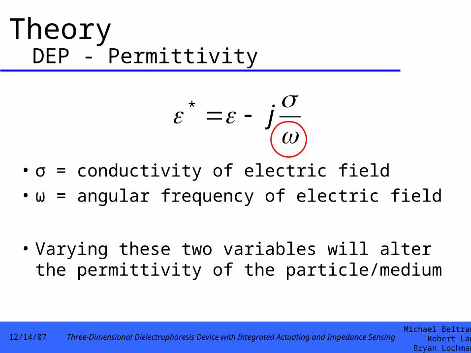
• σ = conductivity of electric field
• ω = angular frequency of electric field
• Varying these two variables will alter the permittivity of the particle/medium
j*
TheoryDEP - Permittivity

Michael BeltranRobert Lam
Bryan Lochman
12/14/07 Three-Dimensional Dielectrophoresis Device with Integrated Actuating and Impedance Sensing
• At low frequences:
• At high frequencies:
• Polarization Factor (K) can be switched between positive or negative values
mp
mpK2
mp
mpK
2
TheoryDEP - Clausius-Mossotti

Michael BeltranRobert Lam
Bryan Lochman
12/14/07 Three-Dimensional Dielectrophoresis Device with Integrated Actuating and Impedance Sensing
• Buoyancy Force:
• DEP and Buoyancy:
grF mpB 3
3
4
m
mp gEK
3
2]Re[ 2
TheoryDEP – Vertical Forces
Iliescu, C.; Yu, L.; Xu, G.; Tay, F. A Dielectrophoretic Chip With a 3-D Electric Field Gradient, Journal of Microelectromechanical Systems, 2006, 15, 1506-1513

Michael BeltranRobert Lam
Bryan Lochman
12/14/07 Three-Dimensional Dielectrophoresis Device with Integrated Actuating and Impedance Sensing
• FDEP = volume (~r3)
• Fviscous = surface (~r2)
• Smaller particles will move slower
rF
F
visc
DEP
TheoryDEP – Ratio between DEP, Viscous forces

Michael BeltranRobert Lam
Bryan Lochman
12/14/07 Three-Dimensional Dielectrophoresis Device with Integrated Actuating and Impedance Sensing
• Progressively alternating electrode signals move particles towards target electrode
• Provides better sensing of particles
TheoryDEP – Cage Actuation
Medoro, G.; Manaresi, N.; Leonardi, A.; Altomare, L.; Tartagni, M.; Guerrieri, R. A Lab-on-a-Chip for Cell Detection and Manipulation. IEEE Sensors Journal, 2003, 3, 317-325

Michael BeltranRobert Lam
Bryan Lochman
12/14/07 Three-Dimensional Dielectrophoresis Device with Integrated Actuating and Impedance Sensing
• The DEP Cages are able to move toward a target electrode by moving the counter phase signal to the next electrode closer to the target
TheoryDEP – Cage Actuation
Medoro, G.; Manaresi, N.; Leonardi, A.; Altomare, L.; Tartagni, M.; Guerrieri, R. A Lab-on-a-Chip for Cell Detection and Manipulation. IEEE Sensors Journal, 2003, 3, 317-325
Michael BeltranRobert Lam
Bryan Lochman
12/14/07 Three-Dimensional Dielectrophoresis Device with Integrated Actuating and Impedance Sensing
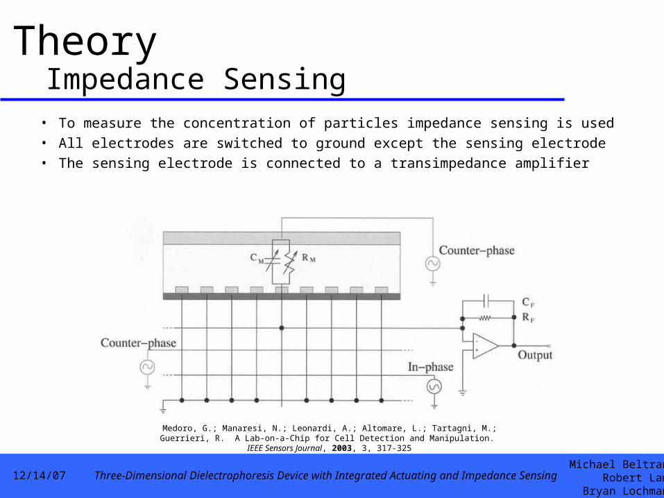
• To measure the concentration of particles impedance sensing is used• All electrodes are switched to ground except the sensing electrode• The sensing electrode is connected to a transimpedance amplifier
TheoryImpedance Sensing
Medoro, G.; Manaresi, N.; Leonardi, A.; Altomare, L.; Tartagni, M.; Guerrieri, R. A Lab-on-a-Chip for Cell Detection and Manipulation. IEEE Sensors Journal, 2003, 3, 317-325

Michael BeltranRobert Lam
Bryan Lochman
12/14/07 Three-Dimensional Dielectrophoresis Device with Integrated Actuating and Impedance Sensing
• Transfer function of the transimpedance amplifier:
• RM and CM are the resistance and capacitance between the electrode and lid
• RF and CF are the feedback resistance and capacitance
• There are two sensing frequency ranges, low and high, if the same signal is used for both DEP cage formation and sensing
FF
MM
M
F
i
o
CjwR
CjwR
R
Rjw
V
V
1
1)(
TheoryImpedance Sensing – Transfer Function

Michael BeltranRobert Lam
Bryan Lochman
12/14/07 Three-Dimensional Dielectrophoresis Device with Integrated Actuating and Impedance Sensing
• Low Frequency– When w<<1/(RMCM) and w<<1/(RFCF) the sensing equation is:
– The Clausius Mossotti factor at low frequencies,
shows that a particle will only be trapped in the DEP cage if its conductivity is lower than the mediums giving rise to :
– These two equations show the output voltage will decrease with particles at low frequencies
M
F
i
o
R
R
V
V
mp
mpK2
TheoryImpedance Sensing at low frequencies
wopM
wpM RR

Michael BeltranRobert Lam
Bryan Lochman
12/14/07 Three-Dimensional Dielectrophoresis Device with Integrated Actuating and Impedance Sensing
• High Frequency– When w>>1/(RMCM) and w>>1/(RFCF) the sensing equation is:
– The Clausius Mossotti factor at high frequencies,
shows that a particle will only be trapped in the DEP cage if its permittivity is lower than the mediums giving rise to :
– These two equations show the output voltage will decrease with particles at high frequencies
F
M
i
o
C
C
V
V
mp
mpK
2
wopM
wpM CC
TheoryImpedance Sensing at high frequencies

Michael BeltranRobert Lam
Bryan Lochman
12/14/07 Three-Dimensional Dielectrophoresis Device with Integrated Actuating and Impedance Sensing
Original Fabrication
• No MEMS fabrication methods used
• Printed Circuit Board (PCB) techniques used to attach electrodes– Silk screened the
electrode pattern on to a gold clad board
– etched away the uncovered portion
– remove the screened resist
Medoro, G.; Manaresi, N.; Leonardi, A.; Altomare, L.; Tartagni, M.; Guerrieri, R. A Lab-on-a-Chip for Cell Detection and Manipulation. IEEE Sensors Journal, 2003, 3, 317-325
Michael BeltranRobert Lam
Bryan Lochman
12/14/07 Three-Dimensional Dielectrophoresis Device with Integrated Actuating and Impedance Sensing
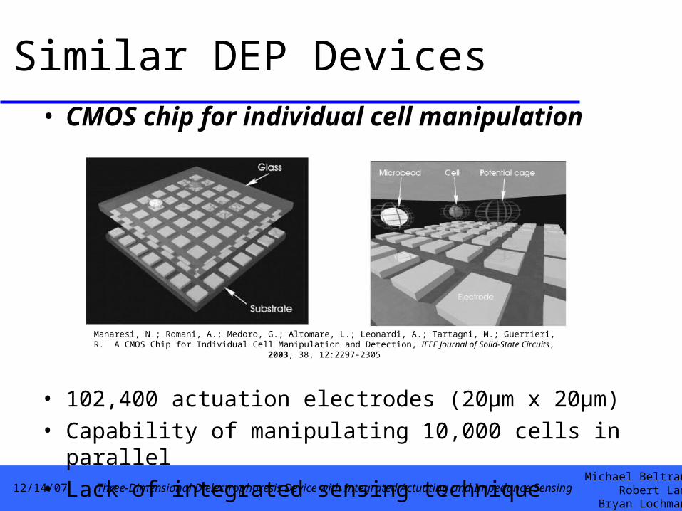
Similar DEP Devices• CMOS chip for individual cell manipulation
• 102,400 actuation electrodes (20μm x 20μm)• Capability of manipulating 10,000 cells in parallel• Lack of integrated sensing technique
Manaresi, N.; Romani, A.; Medoro, G.; Altomare, L.; Leonardi, A.; Tartagni, M.; Guerrieri, R. A CMOS Chip for Individual Cell Manipulation and Detection, IEEE Journal of Solid-State Circuits, 2003, 38, 12:2297-2305

Michael BeltranRobert Lam
Bryan Lochman
12/14/07 Three-Dimensional Dielectrophoresis Device with Integrated Actuating and Impedance Sensing
Similar DEP Devices
• Dielectrophoretic Chip With a 3-D Electric Field Gradient
• Asymmetric 3D electric gradient achieved with specially configured electrodes
• Thick electrodes integrated into vertical wall structures, thin planar electrodes in bottom substrate
• Enhanced vertical DEP force (lower voltages and temperatures)
Iliescu, C.; Yu, L.; Xu, G.; Tay, F. A Dielectrophoretic Chip With a 3-D Electric Field Gradient, Journal of Microelectromechanical Systems, 2006, 15, 1506-1513

Michael BeltranRobert Lam
Bryan Lochman
12/14/07 Three-Dimensional Dielectrophoresis Device with Integrated Actuating and Impedance Sensing
Similar DEP Devices
• MEMS electrostatic particle transportation system
• Electrostatic device capable of transporting particles in air
• Surface modifications performed to reduce adhesive forces
Desai, A.; Lee, S-W.; Tai, Y. A MEMS Electrostatic Particle Transportation System. Sensors and Actuators, 1999, 73, 37-44

Michael BeltranRobert Lam
Bryan Lochman
12/14/07 Three-Dimensional Dielectrophoresis Device with Integrated Actuating and Impedance Sensing
• Parasitic Cages form between the two in-phase electrodes, electrodes 3 and 4 in Figure (a)
• After actuating the DEP cage, a new parasitic cage will form capturing the slow moving particles
(a) (b)
Actuate the DEP Cage
New parasitic DEP Cage
ResultsParasitic Cages
Medoro, G.; Manaresi, N.; Leonardi, A.; Altomare, L.; Tartagni, M.; Guerrieri, R. A Lab-on-a-Chip for Cell Detection and Manipulation. IEEE Sensors Journal, 2003, 3, 317-325

Michael BeltranRobert Lam
Bryan Lochman
12/14/07 Three-Dimensional Dielectrophoresis Device with Integrated Actuating and Impedance Sensing
Parasitic Cages
ResultsParasitic Cages
Medoro, G.; Manaresi, N.; Leonardi, A.; Altomare, L.; Tartagni, M.; Guerrieri, R. A Lab-on-a-Chip for Cell Detection and Manipulation. IEEE Sensors Journal, 2003, 3, 317-325
Michael BeltranRobert Lam
Bryan Lochman
12/14/07 Three-Dimensional Dielectrophoresis Device with Integrated Actuating and Impedance Sensing
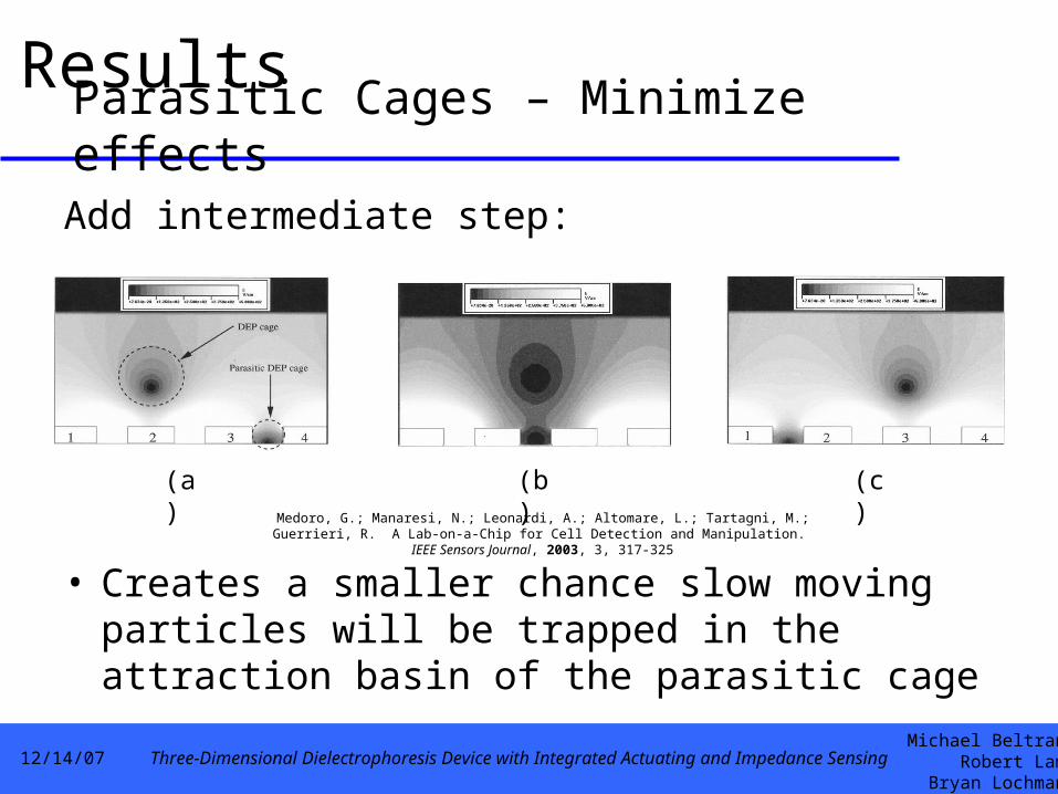
Add intermediate step:
• Creates a smaller chance slow moving particles will be trapped in the attraction basin of the parasitic cage
(a) (b) (c)
ResultsParasitic Cages – Minimize effects
Medoro, G.; Manaresi, N.; Leonardi, A.; Altomare, L.; Tartagni, M.; Guerrieri, R. A Lab-on-a-Chip for Cell Detection and Manipulation. IEEE Sensors Journal, 2003, 3, 317-325

Michael BeltranRobert Lam
Bryan Lochman
12/14/07 Three-Dimensional Dielectrophoresis Device with Integrated Actuating and Impedance Sensing
Reduce space between electrodes:
• Space between electrodes is nearly too small for particles to fit
• Only possible using MEMS fabrication techniques due to small spacing
ResultsParasitic Cages – Minimize effects
Medoro, G.; Manaresi, N.; Leonardi, A.; Altomare, L.; Tartagni, M.; Guerrieri, R. A Lab-on-a-Chip for Cell Detection and Manipulation. IEEE Sensors Journal, 2003, 3, 317-325

Michael BeltranRobert Lam
Bryan Lochman
12/14/07 Three-Dimensional Dielectrophoresis Device with Integrated Actuating and Impedance Sensing
ResultsModeling Assumptions
• Cage distribution far too complicated to be modeled at the level of individual particles
Assumptions• Particle cloud within the DEP cage can be
modeled as homogenous• Permittivity and Conductivity depend solely on
the ratio between the volume of microbeads and suspending medium in the cylinder (distilled water).

Michael BeltranRobert Lam
Bryan Lochman
12/14/07 Three-Dimensional Dielectrophoresis Device with Integrated Actuating and Impedance Sensing
ResultsSignal Processing
•Fixed pattern noise (FPN) removed by subtracting initial non-cage reading (a) from cage reading, and then addition of average initial reading.
Medoro, G.; Manaresi, N.; Leonardi, A.; Altomare, L.; Tartagni, M.; Guerrieri, R. A Lab-on-a-Chip for Cell Detection and Manipulation. IEEE Sensors Journal, 2003, 3, 317-325

Michael BeltranRobert Lam
Bryan Lochman
12/14/07 Three-Dimensional Dielectrophoresis Device with Integrated Actuating and Impedance Sensing
ResultsOptical observation
• Polystyrene microbeads, 3.46 µm diameter in H2O.
• 10 Vpp, 100 kHz • 4 Concentration cycles• Raw data on left• Grayscale representation
of data on right
Medoro, G.; Manaresi, N.; Leonardi, A.; Altomare, L.; Tartagni, M.; Guerrieri, R. A Lab-on-a-Chip for Cell Detection and Manipulation. IEEE Sensors Journal, 2003, 3, 317-325

Michael BeltranRobert Lam
Bryan Lochman
12/14/07 Three-Dimensional Dielectrophoresis Device with Integrated Actuating and Impedance Sensing
• Electric field simulation in FEMLAB in a 2-D plane
• Simulation performed for initial concentration and 4 successive concentration cycles
• Resistance translated to voltage output with known current
ResultsPolystyrene Microbeads
Medoro, G.; Manaresi, N.; Leonardi, A.; Altomare, L.; Tartagni, M.; Guerrieri, R. A Lab-on-a-Chip for Cell Detection and Manipulation. IEEE Sensors Journal, 2003, 3, 317-325

Michael BeltranRobert Lam
Bryan Lochman
12/14/07 Three-Dimensional Dielectrophoresis Device with Integrated Actuating and Impedance Sensing
• Experiment repeated with S. cerevisiae yeast cells in 280-mM mannitol.
• Mannitol medium used to prevent overheating due to excessive conductivity
• S. cerevisiae displays pDEP behavior above 200 kHz, electrolysis occurs at less than 30 kHz
• Experiments performed at 100 kHz
ResultsS. cerevisia
Medoro, G.; Manaresi, N.; Leonardi, A.; Altomare, L.; Tartagni, M.; Guerrieri, R. A Lab-on-a-Chip for Cell Detection and Manipulation. IEEE Sensors Journal, 2003, 3, 317-325

Michael BeltranRobert Lam
Bryan Lochman
12/14/07 Three-Dimensional Dielectrophoresis Device with Integrated Actuating and Impedance Sensing
Recommendations
• Base layer of SiO2 with photoresist on Silicon
Micro-fabrication

Michael BeltranRobert Lam
Bryan Lochman
12/14/07 Three-Dimensional Dielectrophoresis Device with Integrated Actuating and Impedance Sensing
Recommendations
• Mask pattern, inverted from intended electrode pattern
Micro-fabrication

Michael BeltranRobert Lam
Bryan Lochman
12/14/07 Three-Dimensional Dielectrophoresis Device with Integrated Actuating and Impedance Sensing
Recommendations
• Exposure to light – removal of photoresist.
Micro-fabrication

Michael BeltranRobert Lam
Bryan Lochman
12/14/07 Three-Dimensional Dielectrophoresis Device with Integrated Actuating and Impedance Sensing
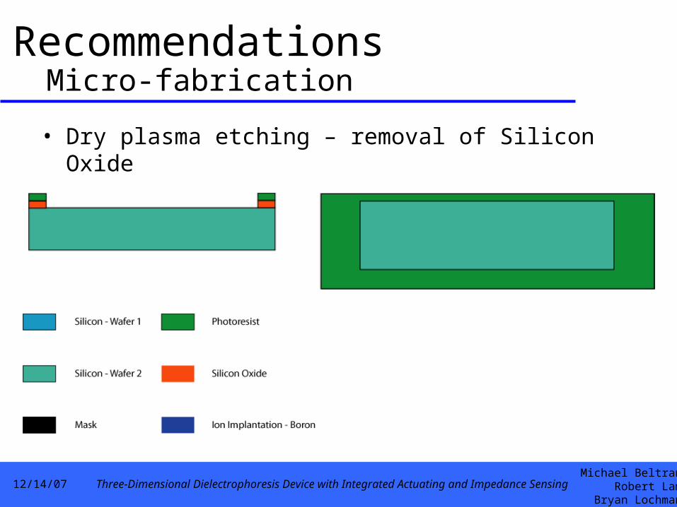
Recommendations
• Dry plasma etching – removal of Silicon Oxide
Micro-fabrication

Michael BeltranRobert Lam
Bryan Lochman
12/14/07 Three-Dimensional Dielectrophoresis Device with Integrated Actuating and Impedance Sensing
Recommendations
• Removal of photoresist with acetone
Micro-fabrication

Michael BeltranRobert Lam
Bryan Lochman
12/14/07 Three-Dimensional Dielectrophoresis Device with Integrated Actuating and Impedance Sensing
Recommendations
• Ion implantation of electrode channels
Micro-fabrication

Michael BeltranRobert Lam
Bryan Lochman
12/14/07 Three-Dimensional Dielectrophoresis Device with Integrated Actuating and Impedance Sensing
Recommendations
• Removal of silicon oxide via plasma etching with CF4
Micro-fabrication

Michael BeltranRobert Lam
Bryan Lochman
12/14/07 Three-Dimensional Dielectrophoresis Device with Integrated Actuating and Impedance Sensing
Recommendations
• Lap polish of wafer to 50μm thickness
Micro-fabrication

Michael BeltranRobert Lam
Bryan Lochman
12/14/07 Three-Dimensional Dielectrophoresis Device with Integrated Actuating and Impedance Sensing
Recommendations
• Growth of SiO2 layers, removal from underside.
Micro-fabrication

Michael BeltranRobert Lam
Bryan Lochman
12/14/07 Three-Dimensional Dielectrophoresis Device with Integrated Actuating and Impedance Sensing
Recommendations
• Spin deposition of photoresist and mask placement
Micro-fabrication

Michael BeltranRobert Lam
Bryan Lochman
12/14/07 Three-Dimensional Dielectrophoresis Device with Integrated Actuating and Impedance Sensing
Recommendations
• Exposure to light - removal of photoresist
Micro-fabrication
Michael BeltranRobert Lam
Bryan Lochman
12/14/07 Three-Dimensional Dielectrophoresis Device with Integrated Actuating and Impedance Sensing
Recommendations
• Dry plasma etching – removal of Silicon Oxide
Micro-fabrication

Michael BeltranRobert Lam
Bryan Lochman
12/14/07 Three-Dimensional Dielectrophoresis Device with Integrated Actuating and Impedance Sensing
Recommendations
• Removal of photoresist with acetone
Micro-fabrication

Michael BeltranRobert Lam
Bryan Lochman
12/14/07 Three-Dimensional Dielectrophoresis Device with Integrated Actuating and Impedance Sensing
Recommendations
• <110> wafer KOH through-etching of silicon wafer
Micro-fabrication

Michael BeltranRobert Lam
Bryan Lochman
12/14/07 Three-Dimensional Dielectrophoresis Device with Integrated Actuating and Impedance Sensing
Recommendations
• Removal of silicon oxide via plasma etching with CF4
Micro-fabrication

Michael BeltranRobert Lam
Bryan Lochman
12/14/07 Three-Dimensional Dielectrophoresis Device with Integrated Actuating and Impedance Sensing
Recommendations
• Combination of base electrode layer and reservoir layer
Micro-fabrication

Michael BeltranRobert Lam
Bryan Lochman
12/14/07 Three-Dimensional Dielectrophoresis Device with Integrated Actuating and Impedance Sensing
Recommendations
• Mated with wafer bonding over long electrodes, leaving wire-connection ports exposed
Micro-fabrication

Michael BeltranRobert Lam
Bryan Lochman
12/14/07 Three-Dimensional Dielectrophoresis Device with Integrated Actuating and Impedance Sensing
Recommendations
• Mass production on a silicon wafer• Glass cover with etched microchannel pattern and
common reservoir
Micro-fabrication