UNIVERSITÀ DEGLI ISTITUTO NAZIONALE
STUDI DI PADOVA DI FISICA NUCLEARE
Facoltà di Scienze MM.NN.FF. Laboratori Nazionali di Legnaro
MASTER THESIS
in
“Surface Treatments for Industrial Applications”
HIGH TEMPERATURE METATHESIS FOR THE PREPARATION OF Nb3GaAl
SUPERCONDUCTORS
Supervisor: Prof. V. Palmieri
Co-Supervisor: Dr. A.A.Rossi
Student: Dr. Andrea M. Camacho Romero
Matr. N°: 1023735
Academic Year 2010-2011
ii
Acknowledgements
Mainly thanks to my whole family who supported me at all the time to achieve this
goal, for the values and education that made possible my personal and academic growth. Today
I am who I am for them.
Second to the professors Laszlo Sajo and Haydn Barros for believe in me.
To the whole excellent superconductivity group for gave me this great opportunity and
share with me. Specifically, Professor Palmieri, Silvia Martin, Antonio Rossi and Oscar
Azzolini.
Last, but not least, to Venezuelan family in Italy, especially to Daniel Adrien Franco
Lespinasse, Winder Alexander, Judilka, Gabriela, Yara, Jesús and Jacobo, for all the support
they have given me.
iii
Abstract
This works deals with the A15 compound synthesis on niobium samples and over the
internal surface of niobium cavities by means of induction heating. Specifically, three
compounds were studied: Nb3Ga, Nb3Al and Nb-Al-Ga. As for the preparation of the niobium
samples, they were treated with BCP solution in order to polish the surface. The niobium
cavities were treated with centrifugal tumbling, BCP solution and high pressure water rising.
Subsequent, the samples, or cavities, were placed into an inductor controlling the voltage, time,
sample position, temperature, type and pressure of gas used. The highest critical temperature
obtained was 18 K and Tc 0,35 K, in Nb-Al-Ga#1 sample by inductive measurement.
Mapping analysis showed the uniform diffusion of aluminum into the niobium, and the gallium
diffuses creating channels into niobium. The composition was measured by EDS obtaining
(82±1)% wt. Niobium, (11,3±0,9)% wt. Gallium, (4,7±0,2)% wt. Aluminum and (1,9±0,1)%
wt. Oxygen. Finally, RF test confirmed that the cavities obtained after the annealing were
normal conductive indicating that the preparation parameters must still be optimized.
Keywords: A15, superconductor, superconducting cavities, induction heating, Nb3GaAl.

iv
CONTENTS
INTRODUCTION ................................................................................................................... 1
CHAPTER 1. LITERATURE REVIEW ......................................................................................... 3
I.1. Particle Accelerators ........................................................................................................... 3
I.2. Superconducting Radio Frequency Resonant Cavities ........................................................ 4
I.3. Physical basis SRF cavities .................................................................................................. 4
I.4. Surface resistance in superconductors ................................................................................. 6
I.5. A15 compounds ................................................................................................................... 7
I.5.1. Nb3Ga ....................................................................................................................................................... 9
I.5.2. Nb3Al ...................................................................................................................................................... 11
I.5.3. Nb3GaAl .................................................................................................................................................. 13
CHAPTER 2. EXPERIMENTAL PROCEDURE ........................................................................... 17
II.1. Induction Heating System ................................................................................................. 17
II.2. Samples and cavities preparation ...................................................................................... 19
II.3. A15 preparation .............................................................................................................. 22
CHAPTER 3. RESULTS AND DISCUSSION .............................................................................. 27
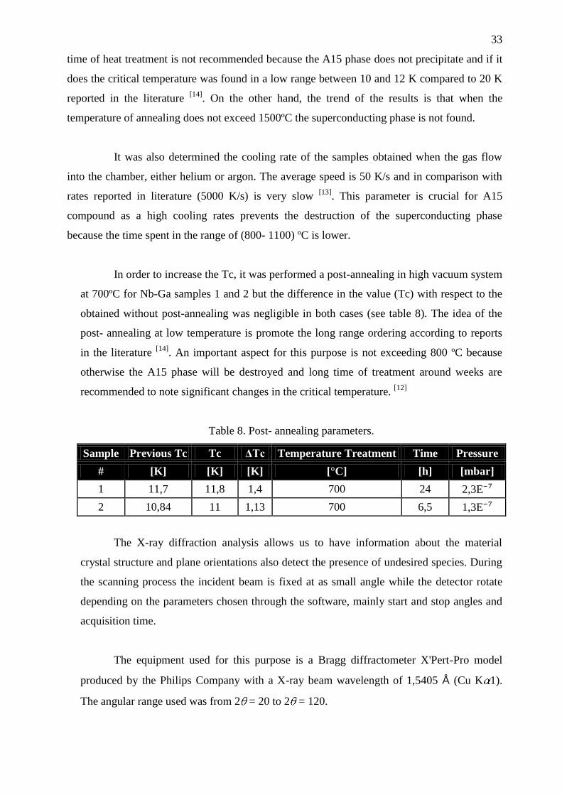
III.1. Nb3Ga samples ................................................................................................................ 28
III.2. Nb3Al samples ................................................................................................................. 35
III.3. Nb3AlGa samples ............................................................................................................. 40
III.4. Cavities ............................................................................................................................ 56
CHAPTER 4. CONCLUSIONS ................................................................................................ 60
CHAPTER 5. RECOMMENDATIONS ..................................................................................... 61
CHAPTER 6. BIBLIOGRAPHY ............................................................................................... 62
ANNEXES.............................................................................................................................64

INTRODUCTION
Nowadays, technological advances in particle accelerators are focus according to the
physical needs, such as nuclear physics, free- electron lasers, high energy particles physic
and neutron spallation sources, which allows solving human needs related to medicine,
space exploration and electronic technology. [1]
Superconducting radio frequency (SRF) technology is based on bulk niobium
cavities that allow higher acceleration gradients compared to conventional copper cavities
because of lower electrical losses. SRF properties are inherently a surface phenomenon
because it is shallow the penetration depth of the radio frequency fields: less than one
micron of thickness. For this reason, and for the high cost of niobium, the thin film coating
technique is a great benefit to fabricate superconducting cavities. [2]
The development of different deposition techniques for thin films and
superconducting materials are on the top of the technological revolution in this field.
Therefore, the general objective is to implement the methodology for performing thin films
of A15 compounds on the internal walls of the 6 GHz niobium dummy cavities by means of
induction heating.
Within the specific objectives there are the following:
Performing preliminary studies of Nb3Ga, Nb3Al and Nb-Al-Ga samples before
initiating the studies with 6 GHz niobium cavities, in order to observe the feasibility
of obtaining good results.
Ensuring the optimal parameters of heat treatment by the inductor, so that it is
reproducible.
Characterizing the samples and cavities with a thin film of A15 compound,
specifically, determine the critical temperature, the Q value, chemical composition,
crystal structure and microscopic properties of the coatings.
Finally, it will be shown the study performed with the work group of superconductivity
lab -INFN illustrating the possible parameters to continue this research project and achieve
the goal of increasing the performance of the cavities for particle accelerators, employing a
new technique and A15 compounds without the need of ultra-high vacuum system.
2
HIGH TEMPERATURE METATHESIS FOR THE PREPARATION OF Nb3GaAl
SUPERCONDUCTORS
INTRODUCTION
LITERATURE REVIEW
Particle Accelerators
Superconducting Radio Frequency Resonant Cavities
Physical basis SRF cavities
Surface resistance in superconductors
A15 compounds
Nb3Ga
Nb3Al
Nb3GaAl
EXPERIMENTAL PROCEDURE
Induction heating system
Samples and cavities preparation
A15 preparation
RESULTS AND DISCUSSION
Nb3Ga samples
Nb3Al samples
Nb3AlGa samples
Cavities CONCLUSIONS
RECOMMENDATIONS
3
CHAPTER 1. LITERATURE REVIEW
I.1. Particle Accelerators
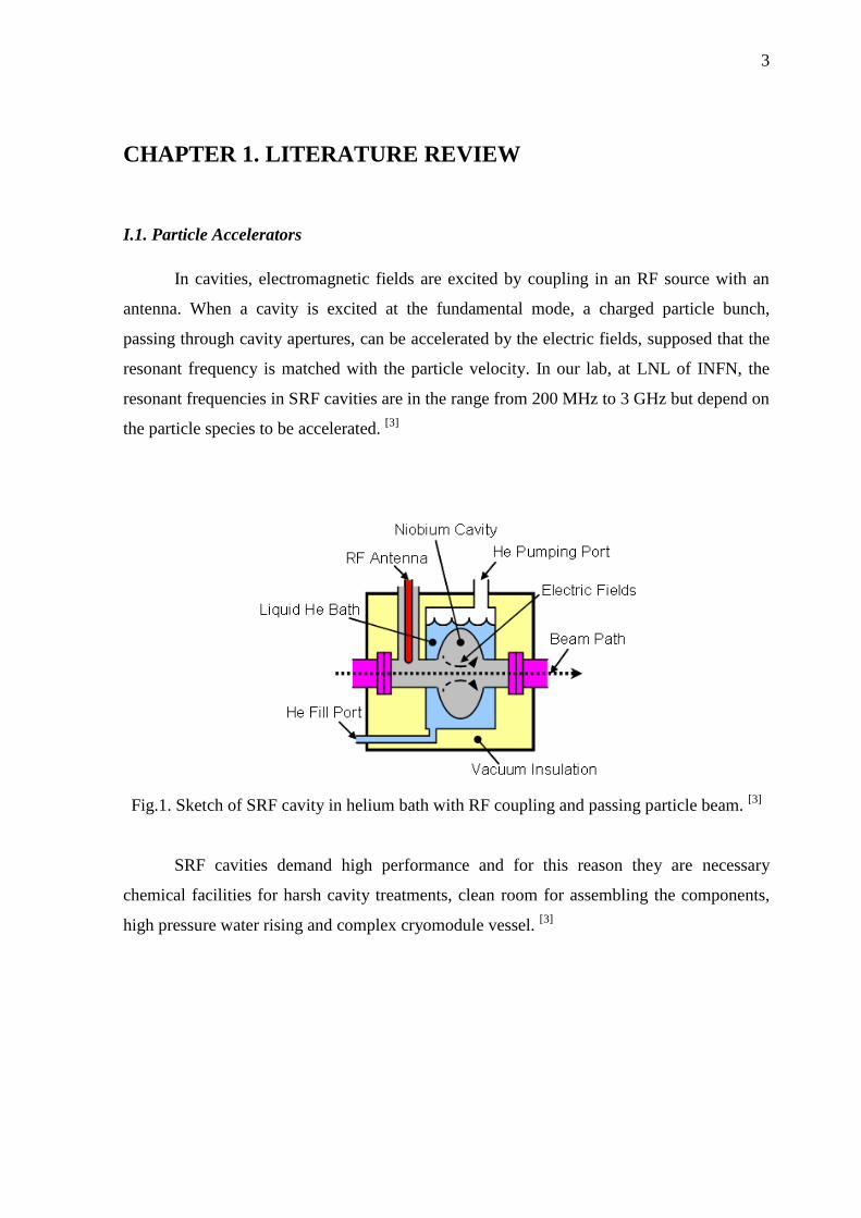
In cavities, electromagnetic fields are excited by coupling in an RF source with an
antenna. When a cavity is excited at the fundamental mode, a charged particle bunch,
passing through cavity apertures, can be accelerated by the electric fields, supposed that the
resonant frequency is matched with the particle velocity. In our lab, at LNL of INFN, the
resonant frequencies in SRF cavities are in the range from 200 MHz to 3 GHz but depend on
the particle species to be accelerated. [3]
Fig.1. Sketch of SRF cavity in helium bath with RF coupling and passing particle beam. [3]
SRF cavities demand high performance and for this reason they are necessary
chemical facilities for harsh cavity treatments, clean room for assembling the components,
high pressure water rising and complex cryomodule vessel. [3]
4
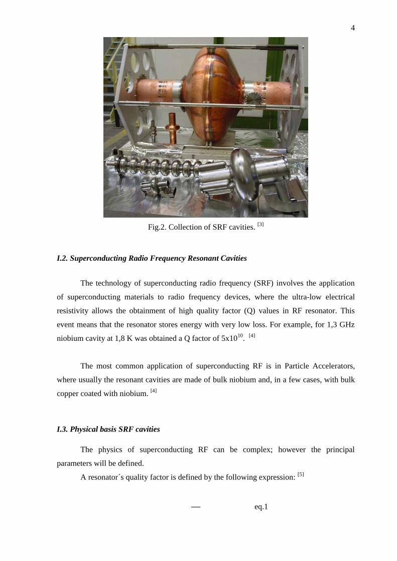
Fig.2. Collection of SRF cavities. [3]
I.2. Superconducting Radio Frequency Resonant Cavities
The technology of superconducting radio frequency (SRF) involves the application
of superconducting materials to radio frequency devices, where the ultra-low electrical
resistivity allows the obtainment of high quality factor (Q) values in RF resonator. This
event means that the resonator stores energy with very low loss. For example, for 1,3 GHz
niobium cavity at 1,8 K was obtained a Q factor of 5x10¹⁰
. [4]
The most common application of superconducting RF is in Particle Accelerators,
where usually the resonant cavities are made of bulk niobium and, in a few cases, with bulk
copper coated with niobium. [4]
I.3. Physical basis SRF cavities
The physics of superconducting RF can be complex; however the principal
parameters will be defined.
A resonator´s quality factor is defined by the following expression: [5]
eq.1

5
Where:
is the resonant frequency [rad/s]
U is the energy stored [J]
Pd is the power dissipated in the cavity [W]
The energy stored in the cavity is given by the integral of field energy density over
its volume: [5]
eq. 2
Where: H is the magnetic field in the cavity and μ0 is the permeability of free space.
The power dissipated is given by the integral of resistive wall losses over its surface:
eq.3
Where: Rs is the surface resistance.
The integrals of the electromagnetic field in the above expressions are generally not
solved analytically; therefore, the calculations are performed by computer programs that
solve for non-simple cavity shapes. Another alternative is determinate Geometry Factor (G)
which is given by the following expression: [5]
eq.4
Then, the Q factor can be obtained by:
eq.5
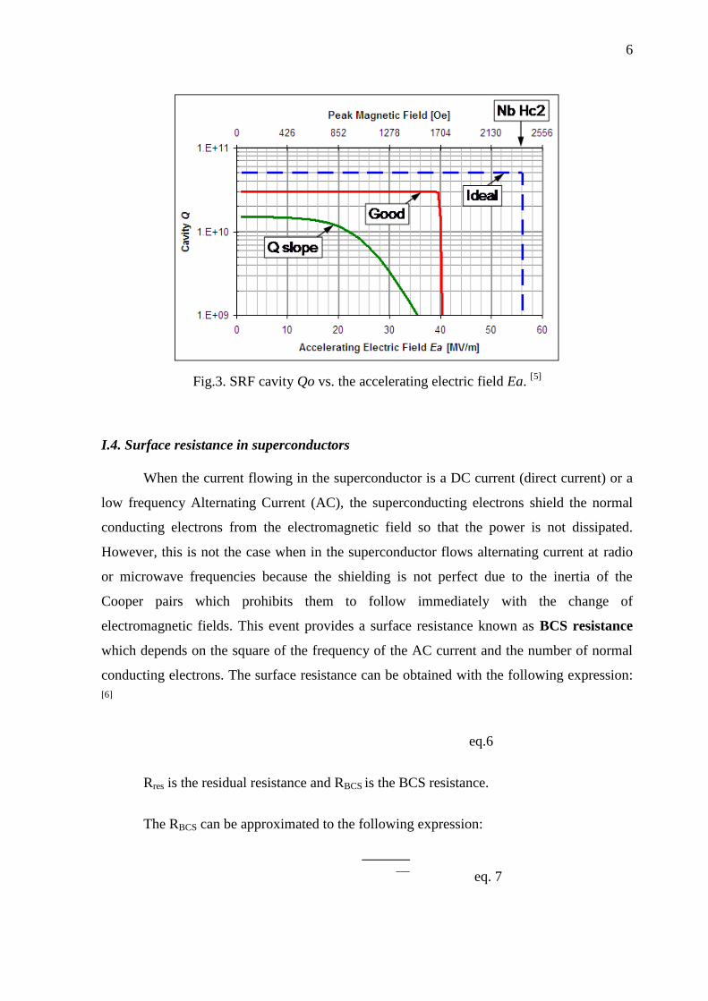
In the superconducting RF cavities for particle accelerators, the field level in the
cavity should be as high as possible to most efficiently accelerate the beam passing through
it. The Qo values tend to degrade as the fields increase, showed in "Q vs E" curve, where
"E" refers to the accelerating electric field. Ideally, the cavity Qo would remain constant as
the accelerating field is increased up to the point of a magnetic quench field (Hc2), but in
reality, is quenching before due to impurities, hydrogen contamination and a rough surface
finish. [5]
6
Fig.3. SRF cavity Qo vs. the accelerating electric field Ea. [5]
I.4. Surface resistance in superconductors
When the current flowing in the superconductor is a DC current (direct current) or a
low frequency Alternating Current (AC), the superconducting electrons shield the normal
conducting electrons from the electromagnetic field so that the power is not dissipated.
However, this is not the case when in the superconductor flows alternating current at radio
or microwave frequencies because the shielding is not perfect due to the inertia of the
Cooper pairs which prohibits them to follow immediately with the change of
electromagnetic fields. This event provides a surface resistance known as BCS resistance
which depends on the square of the frequency of the AC current and the number of normal
conducting electrons. The surface resistance can be obtained with the following expression:
[6]
eq.6
Rres is the residual resistance and RBCS is the BCS resistance.
The RBCS can be approximated to the following expression:
eq. 7
7
Where:
S is the strong coupling factor (~2).
n is the normal state resistivity in DC.
Tc is the critical temperature.
T is the operational temperature.
Then Equation 7 tells us that a low RBCS loss superconductor must have a high critical
temperature and the most metallic behavior in the normal state.
I.5. A15 compounds
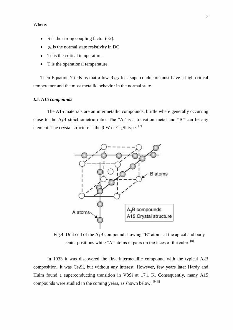
The A15 materials are an intermetallic compounds, brittle where generally occurring
close to the A3B stoichiometric ratio. The “A” is a transition metal and “B” can be any
element. The crystal structure is the β-W or Cr3Si type. [7]
Fig.4. Unit cell of the A3B compound showing “B” atoms at the apical and body
center positions while “A” atoms in pairs on the faces of the cube. [8]
In 1933 it was discovered the first intermetallic compound with the typical A3B
composition. It was Cr3Si, but without any interest. However, few years later Hardy and
Hulm found a superconducting transition in V3Si at 17,1 K. Consequently, many A15
compounds were studied in the coming years, as shown below. [9, 8]

8
In the below table, we can see different values of Tc which is strongly influenced by
the degree of Long-Range crystallographic Order (LRO). In compounds with B atoms are
not a transition metal, the highest Tc value is obtained when all the A atoms are on the A
sites and all the B atoms are on the B sites. This order is quantified through the S parameter
and this parameter reaches the unit, means it has been achieved the Long Range Order. On
the other hand, when the B atoms are not a metal transition, the compound does not have the
same sensitivity to order. [7]
Table 1. Superconducting transition temperatures Tc of some A15 compound.
The number of valence electrons is given for each element. [10]
B/A3 Ti Zr V Nb Ta Cr Mo
4 4 5 5 5 6 6
Al 3
11,8 18,8
0,6
Ga 3
16,8 20,3
0,8
In 3
13,9 9,2
Si 4
17,1 19
1,7
Ge 4
11,2 23,2 8 1,2 1,8
Sn 4 5,8 0,9 7 18 8,4
Pb 4
0,8
8 17
As 5
0,2
Sb 5 5,8
0,8 2,2 0,7
Bi 5
3,4
4,5
Tc 7
15
Re 7
15
Ru 8
3,4 10,6
Os 8
5,7 1,1
4,7 12,7
Rh 9
1 2,6 10 0,3
Ir 9 5,4
1,7 3,2 6,6 0,8 9,6
Pd 9
0,08
Pt 10 0,5
3,7 10,9 0,4
8,8
Au 11 0,9 3,2 11,5 16
9
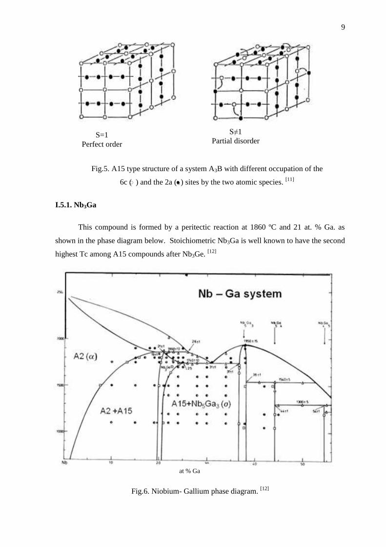
Fig.5. A15 type structure of a system A3B with different occupation of the
6c ( ) and the 2a ( ) sites by the two atomic species. [11]
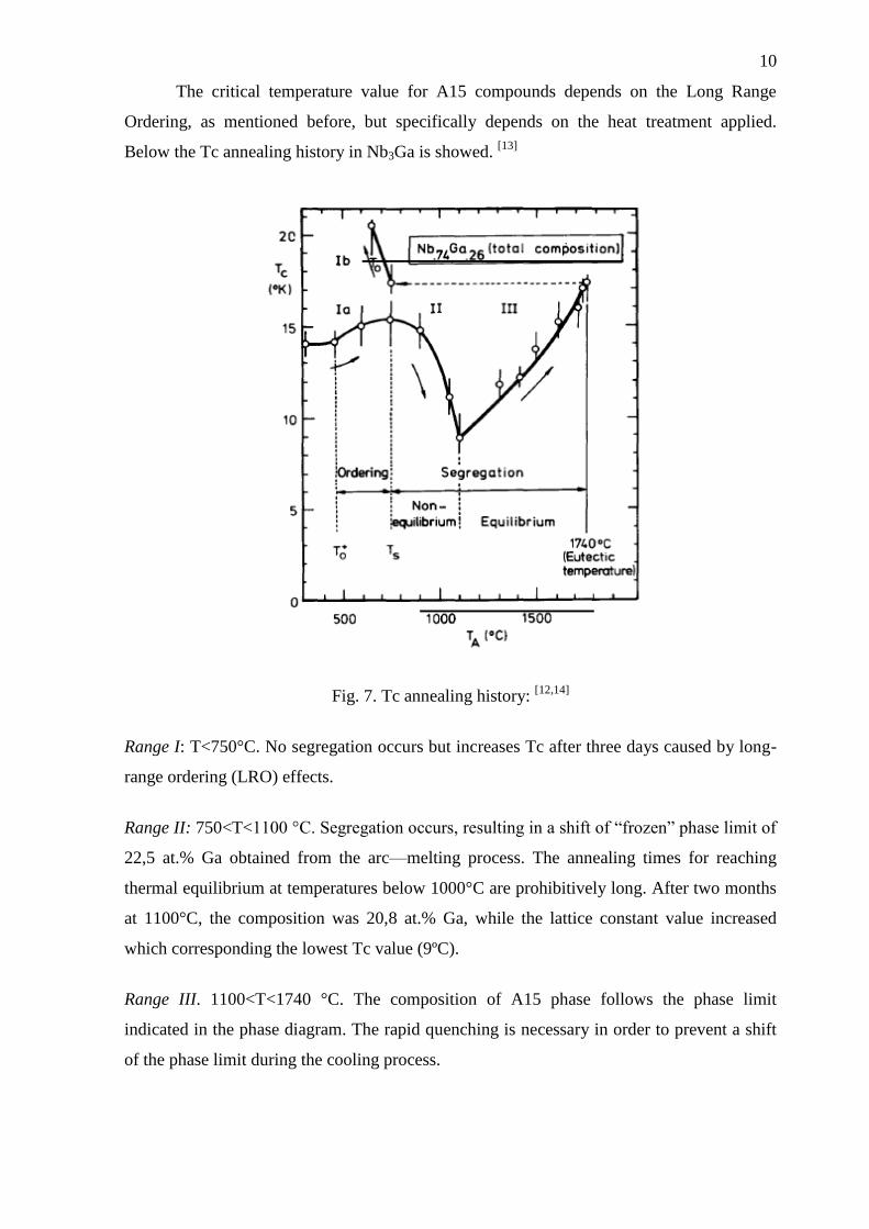
I.5.1. Nb3Ga
This compound is formed by a peritectic reaction at 1860 ºC and 21 at. % Ga. as
shown in the phase diagram below. Stoichiometric Nb3Ga is well known to have the second
highest Tc among A15 compounds after Nb3Ge. [12]
Fig.6. Niobium- Gallium phase diagram. [12]
S=1
Perfect order
S≠1
Partial disorder
at % Ga
10
The critical temperature value for A15 compounds depends on the Long Range
Ordering, as mentioned before, but specifically depends on the heat treatment applied.
Below the Tc annealing history in Nb3Ga is showed. [13]
Fig. 7. Tc annealing history: [12,14]
Range I: T<750°C. No segregation occurs but increases Tc after three days caused by long-
range ordering (LRO) effects.
Range II: 750<T<1100 °C. Segregation occurs, resulting in a shift of “frozen” phase limit of
22,5 at.% Ga obtained from the arc—melting process. The annealing times for reaching
thermal equilibrium at temperatures below 1000°C are prohibitively long. After two months
at 1100°C, the composition was 20,8 at.% Ga, while the lattice constant value increased
which corresponding the lowest Tc value (9ºC).
Range III. 1100<T<1740 °C. The composition of A15 phase follows the phase limit
indicated in the phase diagram. The rapid quenching is necessary in order to prevent a shift
of the phase limit during the cooling process.

11
Fig. 8. Lattice parameter obtained as function of Critical temperature for
Nb3Ga. [12, 14]
Table 2. Nb3Ga properties. [15]
Critical temperature 20 [K]
High Hc2 (4,2 K) Above 30 [T]
Max. Jc (4,2 K) on wires 280 [A/mm2]
Lattice parameter 5,163 [Å]
I.5.2. Nb3Al
This compound is obtained by the peritectic reaction at 2060 ºC and 22,5 at.% Al.
The stoichiometric composition is metastable at room temperature and is only stable at 1940
ºC. The homogeneity range is found at 1000ºC between 19 and 22 at.% Al. [16]
5.165 5.170 5.175 5.180

12
Fig. 9. Niobium- Aluminum phase diagram. [17]
Table 3. Nb3Al properties. [17]
Critical temperature 18,8 [K]
High Hc2 (4,2 K) Above 30 [T]
Max. Jc (4,2 K) at 20 T 105 [A/cm
2]
Lattice parameter at 18,2 K 5,183 [Å]
Fig.10. Critical magnetic fields (Hc2) as a function temperature for three materials.[14]

13
High temperature process around 1800ºC and 2000 ºC consists of continuous heating
and quenching, then retransformed from BCC to A15 at 850 ºC, as shown in the figure
bellow. [18,19]
Fig. 11. Heat treatment for Nb3Al compound. [19]
I.5.3. Nb3GaAl
The superconducting properties of alloys in the Nb3Al-Nb3Ga system have been
studied by Otto who reported a Tc about 18,4 K for Nb3Al sample, increased up to 18,7 K
when Otto added gallium obtaining Nb3Al0,65Ga0,35. In this system it was observed the A15
phase. [20]

14
Fig.12. Nb-Al-Ga system at 1000ºC. [20]
Table 4. Summary of the lattice parameters and superconducting transition temperatures of
Nb-Al-Ga alloys. [21]

15
16
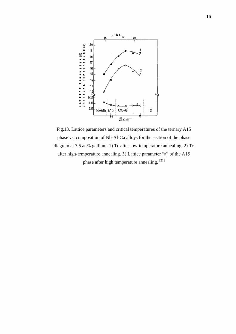
Fig.13. Lattice parameters and critical temperatures of the ternary A15
phase vs. composition of Nb-Al-Ga alloys for the section of the phase
diagram at 7,5 at.% gallium. 1) Tc after low-temperature annealing. 2) Tc
after high-temperature annealing. 3) Lattice parameter “a” of the A15
phase after high temperature annealing. [21]

17
CHAPTER 2. EXPERIMENTAL PROCEDURE
II.1. Induction Heating System
In order to develop RF superconducting A15 cavities was used induction heating
which allows direct heating on samples (or cavities) reaching temperatures higher than
2500ºC. This system has the following advantages compared to the infra-red heating in
ultra-high vacuum system:
Clean quartz tube, where is not found contaminations from chamber or alumina
crucible.
Short time of treatment (few seconds or fractions) instead of hours.
Very high temperatures around 3000ºC. On the contrary, the infra-red heating
reaches no higher than 1100ºC.
The complete system was assembled for the induction heat treat as shown in the figure
below, in order to get the coating of A15 compounds, as the first experimental proof on
niobium samples and then, on niobium cavities.
Fig.14. Sketch of the induction system.
18
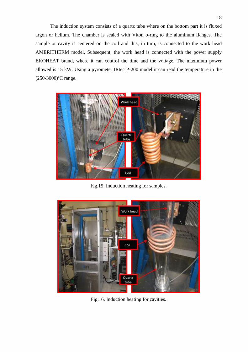
The induction system consists of a quartz tube where on the bottom part it is fluxed
argon or helium. The chamber is sealed with Viton o-ring to the aluminum flanges. The
sample or cavity is centered on the coil and this, in turn, is connected to the work head
AMERITHERM model. Subsequent, the work head is connected with the power supply
EKOHEAT brand, where it can control the time and the voltage. The maximum power
allowed is 15 kW. Using a pyrometer IRtec P-200 model it can read the temperature in the
(250-3000)ºC range.
Fig.15. Induction heating for samples.
Fig.16. Induction heating for cavities.

19
In the figures 15 and 16 it can be observed the induction system; however, it can be
noticed that for cavities the coil and the quartz tube have larger diameter than sample
system.
Fig.17. Left side: Viton o-ring to seal the tube. Right side: Plastic tube on the bottom part
which transports the helium or argon from the bottle into the chamber.
Fig.18. Left side: Power supply where it can set up the voltage and time for the annealing.
Right side: Pyrometers.
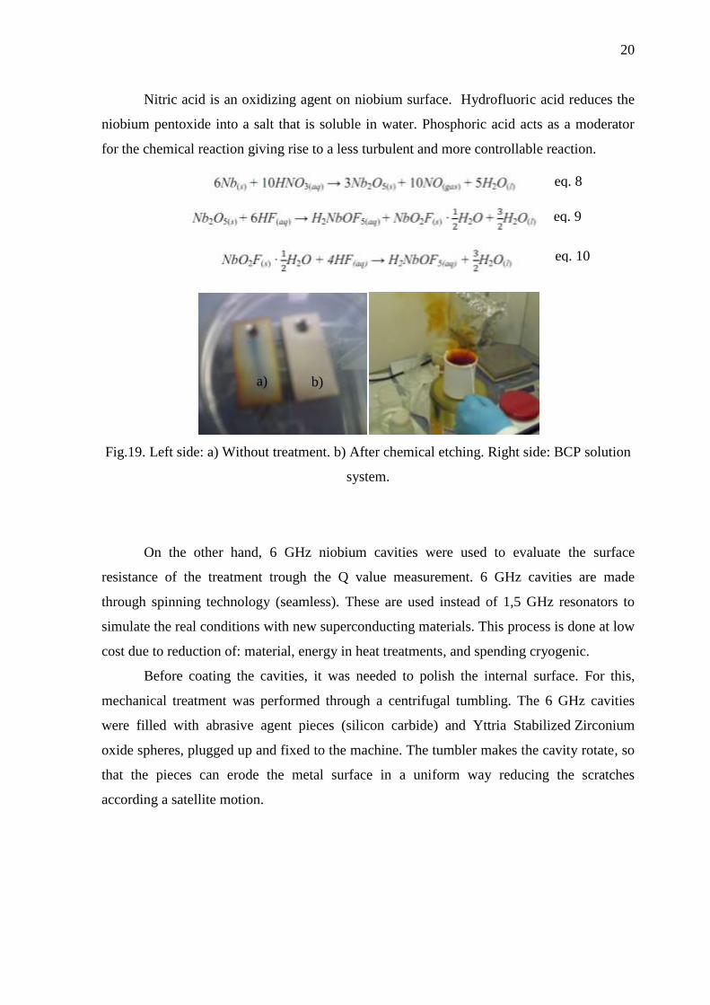
II.2. Samples and cavities preparation
Before coating the niobium samples with A15 compound, these were chemically
etched with BCP (Hydrofluoric acid 40%, Nitric acid 65% and Phosphoric Acid 85%)
solution with a 1:1:2 relation, in order to increase the purity of the sample surface. High rate
reaction was observed when the samples were introduced into the solution as well as brown
gas was observed (NO3).
20
Nitric acid is an oxidizing agent on niobium surface. Hydrofluoric acid reduces the
niobium pentoxide into a salt that is soluble in water. Phosphoric acid acts as a moderator
for the chemical reaction giving rise to a less turbulent and more controllable reaction.
Fig.19. Left side: a) Without treatment. b) After chemical etching. Right side: BCP solution
system.
On the other hand, 6 GHz niobium cavities were used to evaluate the surface
resistance of the treatment trough the Q value measurement. 6 GHz cavities are made
through spinning technology (seamless). These are used instead of 1,5 GHz resonators to
simulate the real conditions with new superconducting materials. This process is done at low
cost due to reduction of: material, energy in heat treatments, and spending cryogenic.
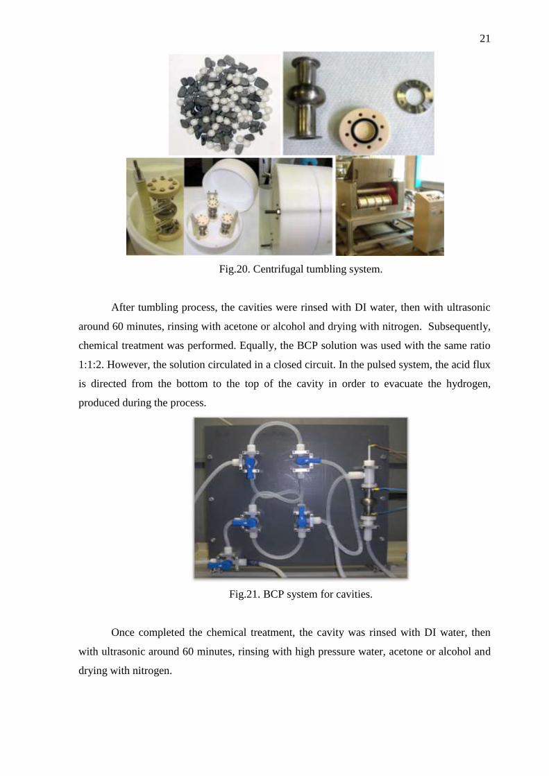
Before coating the cavities, it was needed to polish the internal surface. For this,
mechanical treatment was performed through a centrifugal tumbling. The 6 GHz cavities
were filled with abrasive agent pieces (silicon carbide) and Yttria Stabilized Zirconium
oxide spheres, plugged up and fixed to the machine. The tumbler makes the cavity rotate, so
that the pieces can erode the metal surface in a uniform way reducing the scratches
according a satellite motion.
a) b)
eq. 8
eq. 9
eq. 10
21
Fig.20. Centrifugal tumbling system.
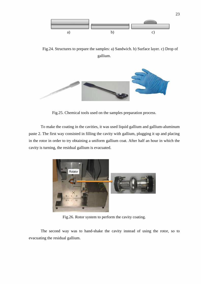
After tumbling process, the cavities were rinsed with DI water, then with ultrasonic
around 60 minutes, rinsing with acetone or alcohol and drying with nitrogen. Subsequently,
chemical treatment was performed. Equally, the BCP solution was used with the same ratio
1:1:2. However, the solution circulated in a closed circuit. In the pulsed system, the acid flux
is directed from the bottom to the top of the cavity in order to evacuate the hydrogen,
produced during the process.
Fig.21. BCP system for cavities.
Once completed the chemical treatment, the cavity was rinsed with DI water, then
with ultrasonic around 60 minutes, rinsing with high pressure water, acetone or alcohol and
drying with nitrogen.

22
Fig.22. High pressure water rinsing with a water jet.
II.3. A15 preparation
In order to perform the coating on niobium samples it was used:
1) Liquid gallium with 99,99% of purity for Nb3Ga samples.
2) Commercial foil, high purity sheet or powder of 200 mesh and 99% purity of
aluminum for Nb3Al samples.
3) For Nb-Al- Ga samples:
a) Liquid gallium + Aluminum sheet.
b) Paste 1: liquid gallium + Aluminum powder.
c) Paste 2: liquid gallium + Aluminum foil.
Fig.23. Aluminum forms used: a) Sheet. b) Commercial foil. c) Powder.
The first way to apply the materials mentioned above was the sandwich structure
which consists in placing the gallium or/and aluminum between two niobium samples. The
second configuration performed was a surface layer without the volume of gallium or
aluminum enclosed. The last system used was a drop of liquid gallium on the niobium
surface. For these three methodologies we used hands, with the appropriated protective
gloves, together with chemical tools as shown in the figure below.
a) b) c)
c)
23
Fig.24. Structures to prepare the samples: a) Sandwich. b) Surface layer. c) Drop of
gallium.
Fig.25. Chemical tools used on the samples preparation process.
To make the coating in the cavities, it was used liquid gallium and gallium-aluminum
paste 2. The first way consisted in filling the cavity with gallium, plugging it up and placing
in the rotor in order to try obtaining a uniform gallium coat. After half an hour in which the
cavity is turning, the residual gallium is evacuated.
Fig.26. Rotor system to perform the cavity coating.
The second way was to hand-shake the cavity instead of using the rotor, so to
evacuating the residual gallium.
a) b) c)

24
Fig.27. Gallium coating performed shaking by hand the cavity.
The third form was to fill completely the cavities with gallium and after perform the
heat treatment without evacuating the gallium, as shown in the figure below.
Fig.28. Third way in order to perform Nb3Ga.
The fourth way was put the liquid gallium with Yttria- stabilized Zirconium oxide
inside the niobium cavity, plug it up and agitate it with both hands. Later, the residual
gallium and Yttria- stabilized Zirconium oxide spheres were evacuated.

25
Fig.29. Fourth way to coat the cavity with gallium.
Last way was using hands with the respective protection gloves i.e. using the fingers
to spread the paste 2 on the internal niobium surface.
Fig.30. Fifth way: coating with Nb-Al-Ga paste 2.
Table 5. Summary of the methodology used in cavities to obtain the A15 compound.
Method Result
Rotor method (with gallium) The coating is not uniform
Hand-shake (with gallium) The coating is not uniform
Heat treatment without evacuate the residual gallium Cavities melted
Gallium with Yttria-stabilized Zirconium spheres The coating is not uniform
Paste 2 coating with fingers Uniform coating
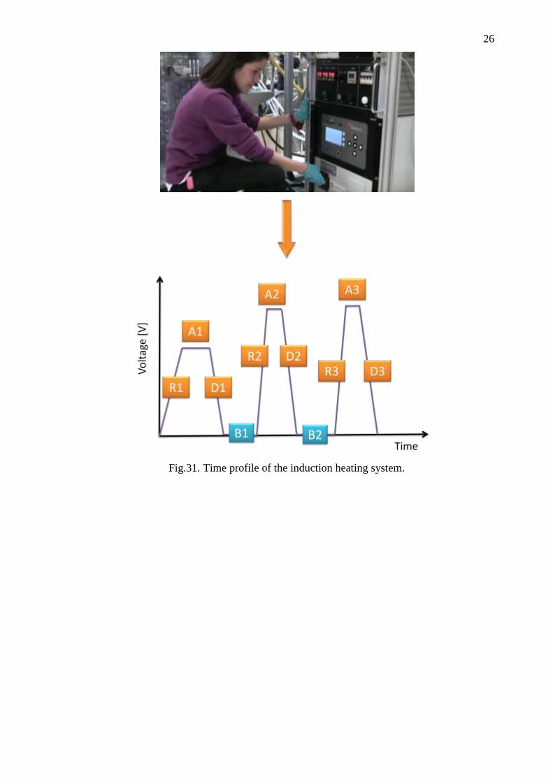
Once obtained the coating of gallium, aluminum, or both, on the niobium surface, it
is necessary the heat treatment with the inductor. We raise the cavity or the sample at high
temperatures close to the melting point, in order to promote the diffusion of these elements
within the niobium, and so to obtain the desired A15 phase. Therefore, the next procedure
carried out was setting the heat treatment profile, specifically the voltage and the time
through the display located on the power supply. However, there are other parameters to
control, such as sample or cavity position, pressure of gas, temperature and type of gas.
Paste 2
26
Fig.31. Time profile of the induction heating system.

27
CHAPTER 3. RESULTS AND DISCUSSION
In total we performed 51 samples with different parameters and 7 cavities by means
of induction heating, distributed as shown below.
Fig.32. Heat treatment by induction.
Table 6. Samples and cavities treated by induction heating.
Performed on Materials Number of samples Total
Samples
Nb-Ga 10
51 Nb-Al 6
Nb-Al-Ga 45
Cavities Nb-Ga 6
7 Nb-Ga-Al 1
After the annealing process, we have to evaluate if we reach the A15 compounds i.e.
the superconducting state. For this, it was used an inductive measurement in order to define
the critical temperature (Tc). The inductive measurement is based on the principle of the
Meissner- Ochsenfeld effect. The superconducting material is placed under a primary coil
that generates an oscillating magnetic field. A secondary coil induces an AC current from
the oscillating field. However, when the superconducting state is reached the material expels
the magnetic field lines that pass through it and the measure phase shift is carried out.
Samples were cooled down with the liquid helium, by dipping the whole set up into the
helium tank.
28
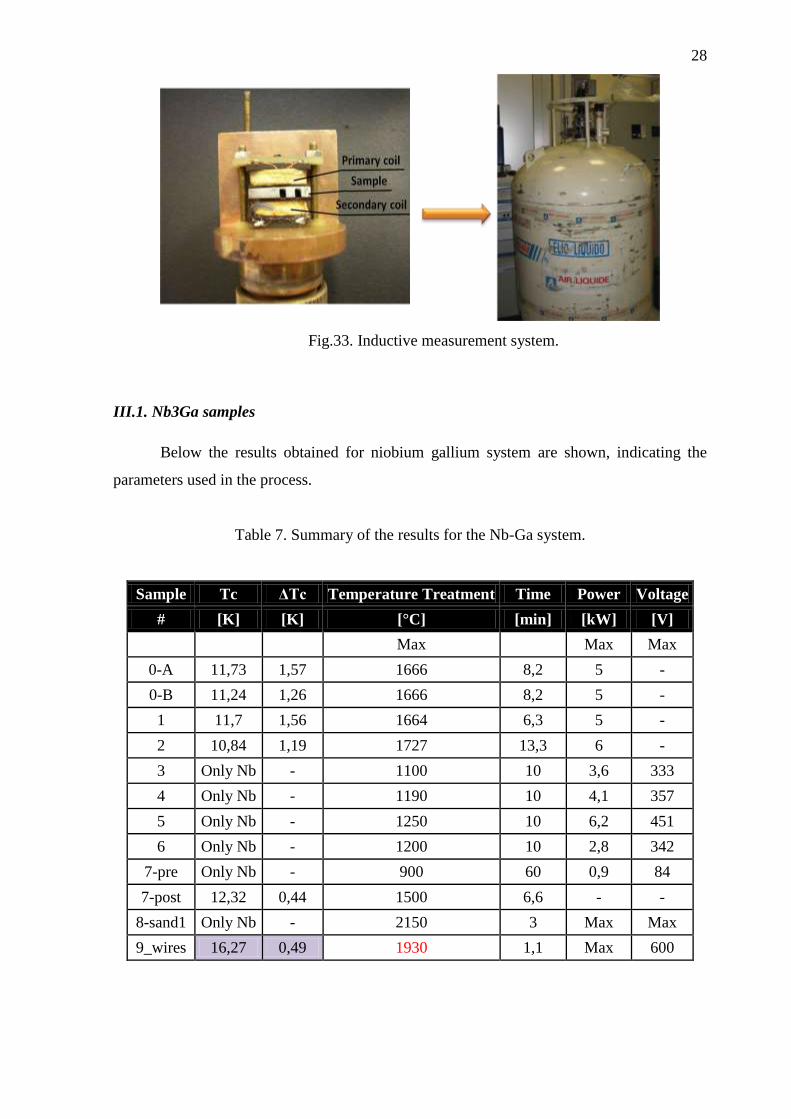
Fig.33. Inductive measurement system.
III.1. Nb3Ga samples
Below the results obtained for niobium gallium system are shown, indicating the
parameters used in the process.
Table 7. Summary of the results for the Nb-Ga system.
Sample Tc ΔTc Temperature Treatment Time Power Voltage
# [K] [K] [°C] [min] [kW] [V]
Max Max Max
0-A 11,73 1,57 1666 8,2 5 -
0-B 11,24 1,26 1666 8,2 5 -
1 11,7 1,56 1664 6,3 5 -
2 10,84 1,19 1727 13,3 6 -
3 Only Nb - 1100 10 3,6 333
4 Only Nb - 1190 10 4,1 357
5 Only Nb - 1250 10 6,2 451
6 Only Nb - 1200 10 2,8 342
7-pre Only Nb - 900 60 0,9 84
7-post 12,32 0,44 1500 6,6 - -
8-sand1 Only Nb - 2150 3 Max Max
9_wires 16,27 0,49 1930 1,1 Max 600

29
The critical temperature (Tc) reported on the before table was determined from the
graphs of the inductive method. These values were calculated from the following
expressions:
Where T (90%) is the temperature in which the resistance has a value equal to 90% of
the transition, T (10%) is the temperature at which the resistance is 10% of the transition. Tc
is an indication of how sharp is the transition.
Fig.34. Phase Shift vs Temperature of the most important transitions obtained by the
sandwich Nb-Ga structure.
0
0,1
0,2
0,3
0,4
0,5
0,6
0,7
0,8
0,9
1
1,1
7 8 9 10 11 12 13 14 15 16 17 18
Ph
S
T [K]
Nb3Ga_ZeroA
Nb3Ga_ZeroB
Nb3Ga_1
Nb3Ga_1_24h
Nb3Ga_2
Nb3Ga_2_6,5h
Nb3Ga_wires
eq. 11
eq. 12

30
Fig.35. Phase Shift vs Temperature for Nb-Ga system where the A15 phase was not found.
According to the figure 34, the highest critical temperature was obtained on the
sample called Nb3Ga_wires (the black one) with a Tc of 16,27 K and Tc 0,49 K. The
conditions used were: maximum temperature of 1930 Cº, maximum voltage (600 V) and 1,1
minutes. The temperature read by the pyrometer is not accurate due to the sensibility i.e. the
temperature on the sample changes faster than the time in which the pyrometer takes the
measure. Also because the camber walls of the induction system were metalized due to the
gallium vapor.
The behavior of the Nb3Ga_wires curve is unusual due to the presence of two
superconducting transitions and between them the resistance increases. The first one at 16,27
K as it was mentioned before and the second one at 13,71 K. This means the presence of the
two different superconducting phases. However, this hypothesis can be corroborated by
analysis of composition and review of the microstructure. Nevertheless, these tests were not
conducted because the sample with highest Tc value was the only thoroughly analyzes and it
was found in the Nb-Al-Ga system.
On the other hand, the Nb3Ga_wire sample and the other samples with transitions
between 10 and 12 K (see figure 34) indicate that obtaining a single phase, specifically the
A15 phase is almost impossible because the region where the phase is stable is very narrow
according to the phase diagram of Nb-Ga system (see figure 6). In addition, when heat
treatment was carried out, we note that the gallium evaporated. The consequence of this fact
is we can´t control the stoichiometry on Nb-Ga samples. As well, we are not certain from the
beginning about how much gallium diffuses into the surface of niobium.
0 0,1
0,2
0,3 0,4
0,5 0,6
0,7 0,8
0,9 1
1,1
6 7 8 9 10 11 12 13 14 15
Ph
S
T [K]
Nb3Ga_3
Nb3Ga_4
Nb3Ga_5
Nb3Ga_6
Nb3Ga_sand1

31
Figure 35 shows the samples of Nb-Ga in which did not precipitate any
superconducting phase. Only the niobium transition was observed. It could be for several
reasons:
1) Complete evaporation of gallium due to the long heat treatment around 10 minutes.
2) The gallium volume was not enclosed since these samples were made with surface
layer and gallium drop configurations.
3) The low wettability of gallium on niobium surface makes the liquid gallium fall as
droplets within the chamber system and it is worse when the temperature is
increasing since the viscosity decreases.
In addition, the gallium handling process was difficult due to the fact that it does not
wet the niobium surface, so not allowing to do the procedure for sandwich arrangement,
gallium drop or surface layer structure (see figure 24) in simple way. Notwithstanding, the
best structure for working at high temperature is the sandwich model because it encloses the
gallium volume decreasing the amount evaporated.
Fig.36. Gallium drop configuration.
Fig.37. Best configuration for samples.

32
Fig.38. Nb-Ga samples obtained after annealing.
Figure 38 shows how the niobium gallium samples look after the heat treatment with
the inductor. In some cases, oxidized samples were found, indicating that it should be
improved or adjusted the sealing system of the chamber. Also, samples showed dark spots
and the surface a little melted as the temperature of the annealing was very high. The control
of the temperature was difficult and very small changes of the time around milliseconds or
on the voltage approximately 5 volts made an important different whether the sample was
melted or not. This implies that the induction system is very sensitive to changes on voltage
and time implemented through the power supply.
Fig.39. Profile of temperature vs. time for Nb3Ga samples.
Figure 39 shows the time at which the sample was subjected to a certain temperature.
According to these profiles and the results of the critical temperature, it can concluded that long
0
500
1000
1500
2000
0 200 400 600 800
Tem
pe
ratu
re (
ºC)
Time (s)
Nb3Ga Zero
Nb3Ga#1
Nb3Ga#2
Nb3Ga#3
Nb3Ga#4
Nb3Ga#5
Nb3Ga#6
Nb3Ga_sand1
Nb3Ga_wires
33
time of heat treatment is not recommended because the A15 phase does not precipitate and if it
does the critical temperature was found in a low range between 10 and 12 K compared to 20 K
reported in the literature [14]
. On the other hand, the trend of the results is that when the
temperature of annealing does not exceed 1500ºC the superconducting phase is not found.
It was also determined the cooling rate of the samples obtained when the gas flow
into the chamber, either helium or argon. The average speed is 50 K/s and in comparison with
rates reported in literature (5000 K/s) is very slow [13]
. This parameter is crucial for A15
compound as a high cooling rates prevents the destruction of the superconducting phase
because the time spent in the range of (800- 1100) ºC is lower.
In order to increase the Tc, it was performed a post-annealing in high vacuum system
at 700ºC for Nb-Ga samples 1 and 2 but the difference in the value (Tc) with respect to the
obtained without post-annealing was negligible in both cases (see table 8). The idea of the
post- annealing at low temperature is promote the long range ordering according to reports
in the literature [14]
. An important aspect for this purpose is not exceeding 800 ºC because
otherwise the A15 phase will be destroyed and long time of treatment around weeks are
recommended to note significant changes in the critical temperature. [12]
Table 8. Post- annealing parameters.
Sample Previous Tc Tc ΔTc Temperature Treatment Time Pressure
# [K] [K] [K] [°C] [h] [mbar]
1 11,7 11,8 1,4 700 24 2,3E⁻⁷
2 10,84 11 1,13 700 6,5 1,3E⁻⁷
The X-ray diffraction analysis allows us to have information about the material
crystal structure and plane orientations also detect the presence of undesired species. During
the scanning process the incident beam is fixed at as small angle while the detector rotate
depending on the parameters chosen through the software, mainly start and stop angles and
acquisition time.
The equipment used for this purpose is a Bragg diffractometer X'Pert-Pro model
produced by the Philips Company with a X-ray beam wavelength of 1,5405 Å (Cu K 1).
The angular range used was from 2 = 20 to 2 = 120.
34
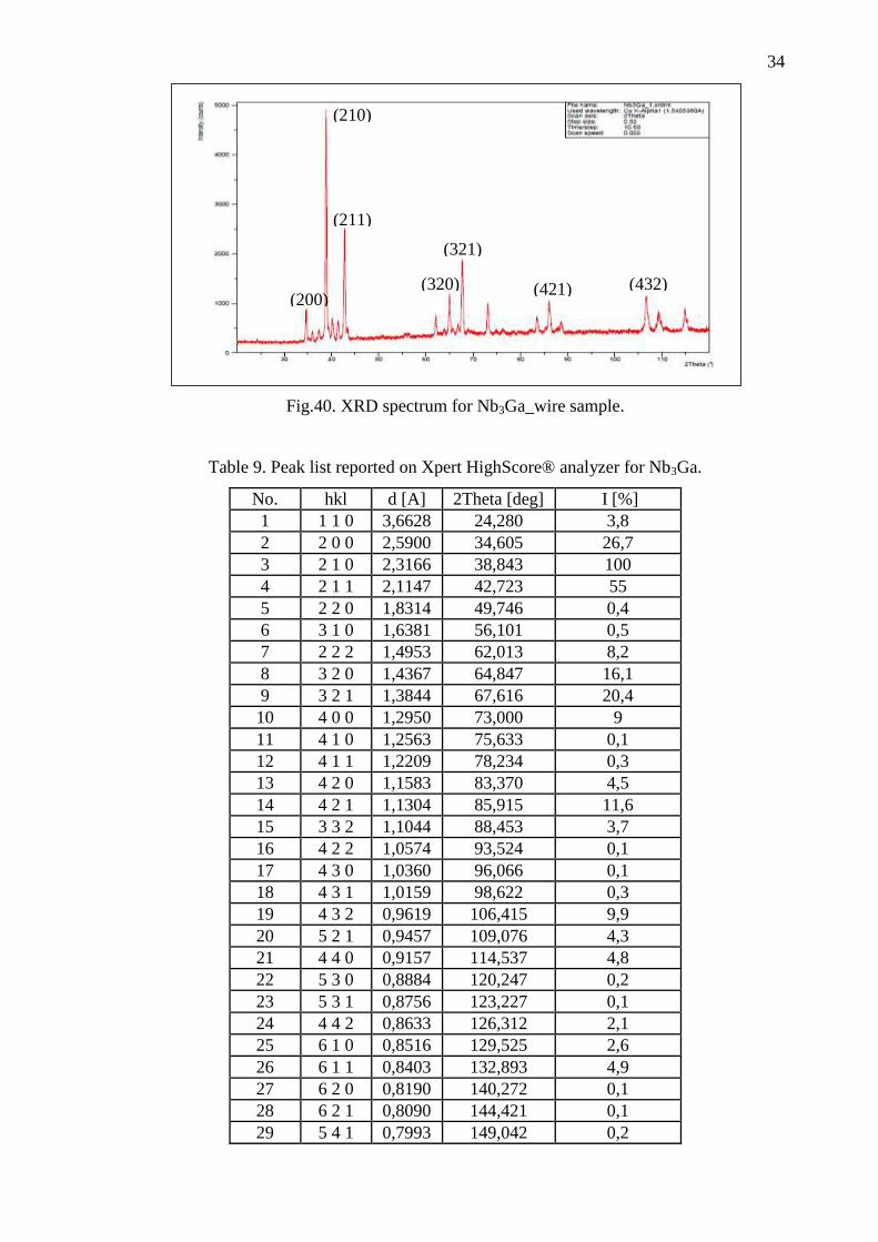
Fig.40. XRD spectrum for Nb3Ga_wire sample.
Table 9. Peak list reported on Xpert HighScore® analyzer for Nb3Ga.
No. hkl d [A] 2Theta [deg] I [%]
1 1 1 0 3,6628 24,280 3,8
2 2 0 0 2,5900 34,605 26,7
3 2 1 0 2,3166 38,843 100
4 2 1 1 2,1147 42,723 55
5 2 2 0 1,8314 49,746 0,4
6 3 1 0 1,6381 56,101 0,5
7 2 2 2 1,4953 62,013 8,2
8 3 2 0 1,4367 64,847 16,1
9 3 2 1 1,3844 67,616 20,4
10 4 0 0 1,2950 73,000 9
11 4 1 0 1,2563 75,633 0,1
12 4 1 1 1,2209 78,234 0,3
13 4 2 0 1,1583 83,370 4,5
14 4 2 1 1,1304 85,915 11,6
15 3 3 2 1,1044 88,453 3,7
16 4 2 2 1,0574 93,524 0,1
17 4 3 0 1,0360 96,066 0,1
18 4 3 1 1,0159 98,622 0,3
19 4 3 2 0,9619 106,415 9,9
20 5 2 1 0,9457 109,076 4,3
21 4 4 0 0,9157 114,537 4,8
22 5 3 0 0,8884 120,247 0,2
23 5 3 1 0,8756 123,227 0,1
24 4 4 2 0,8633 126,312 2,1
25 6 1 0 0,8516 129,525 2,6
26 6 1 1 0,8403 132,893 4,9
27 6 2 0 0,8190 140,272 0,1
28 6 2 1 0,8090 144,421 0,1
29 5 4 1 0,7993 149,042 0,2
(210)
(211)
(321)
(200) (320) (421) (432)
35
According to the X-ray measurement showed in the figure 40 and the software
analyzer Xpert HighScore®, the principal planes of diffraction match with Nb3Ga
compound. The lattice parameter obtained from this measurement was 5,1811 Å and the
standard value is 5,1800 Å but the lattice parameter changes according to long range
ordering in the crystal structure, i.e. the disorder involves greater distortion in the unit cell
and this in turn is reflected in the critical temperature (decreasing Tc). [12]
III.2. Nb3Al samples
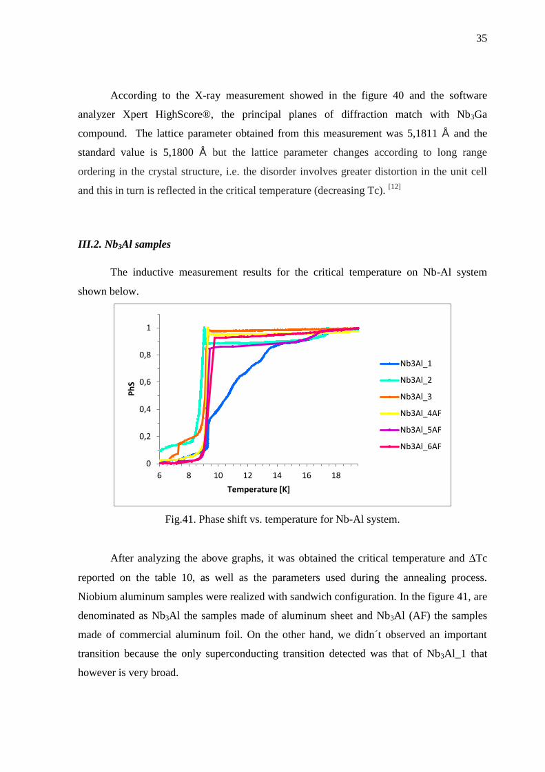
The inductive measurement results for the critical temperature on Nb-Al system
shown below.
Fig.41. Phase shift vs. temperature for Nb-Al system.
After analyzing the above graphs, it was obtained the critical temperature and Tc
reported on the table 10, as well as the parameters used during the annealing process.
Niobium aluminum samples were realized with sandwich configuration. In the figure 41, are
denominated as Nb3Al the samples made of aluminum sheet and Nb3Al (AF) the samples
made of commercial aluminum foil. On the other hand, we didn´t observed an important
transition because the only superconducting transition detected was that of Nb3Al_1 that
however is very broad.
0
0,2
0,4
0,6
0,8
1
6 8 10 12 14 16 18
Ph
S
Temperature [K]
Nb3Al_1
Nb3Al_2
Nb3Al_3
Nb3Al_4AF
Nb3Al_5AF
Nb3Al_6AF

36
Table 10. Critical temperature and parameters used in the annealing process for Nb-Al
system.
Sample Tc ΔTc Temperature Treatment Time Power Voltage
# [K] [K] [°C] [min] [kW] [V]
Max Max Max Max
1 Many transitions - 1700 5 5,9 -
2 17,34 0,1 1520 8,7 2,3 171
3 Only Nb transition - 2060 1,5 Max Max
4 (AF) Only Nb transition - 2061 0,65 -
580 5 (AF) 16,58 0,35 1738 0,63 -
6 (AF) Only Nb transition - 1739 0,6 -
Also, it was evidenced evaporation problems of aluminum at high temperatures,
which metalized the camber walls. As a result, the temperature reading is not accurate, as
well as the contribution due to the pyrometer sensibility. These temperature values are
indicated in the table 10 with red color.
One of the advantages of using aluminum as compared to the gallium is easier to
manipulate, therefore, the process to assemble the sandwich structure was faster. On the
contrary, it was observed that the gallium reacts more than aluminum with the niobium. This
may be due to the corrosive property of the gallium and hence the diffusive process is better.
Over time, we understood that the long time annealing does not form the desired
phase. Consequently, we changed the time of annealing from minutes (around 10 min.) to
few seconds. However, when the annealing process is too short, it is very difficult to control
the temperature switch on/off manually. As a result, we began to configure the times and
voltages for each sample in automated way. Thus, the results can be more reproducible
between samples. The following table shows the set up parameters.
37
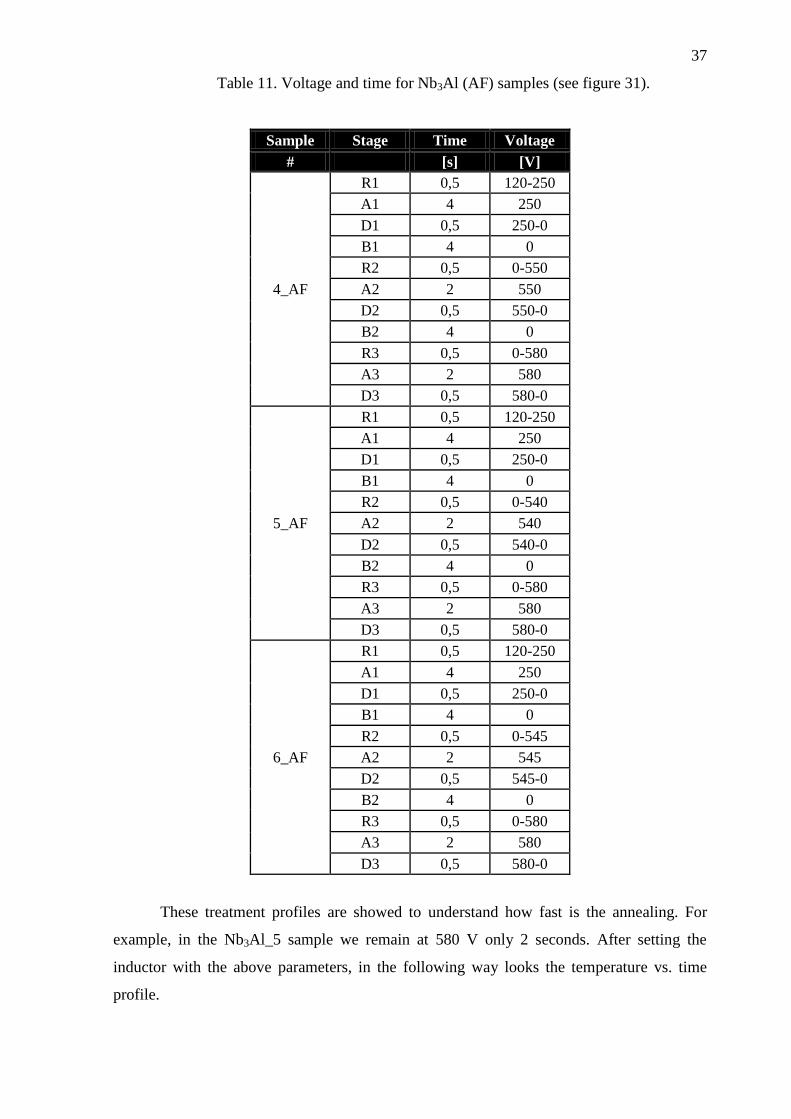
Table 11. Voltage and time for Nb3Al (AF) samples (see figure 31).
Sample Stage Time Voltage
# [s] [V]
4_AF
R1 0,5 120-250
A1 4 250
D1 0,5 250-0
B1 4 0
R2 0,5 0-550
A2 2 550
D2 0,5 550-0
B2 4 0
R3 0,5 0-580
A3 2 580
D3 0,5 580-0
5_AF
R1 0,5 120-250
A1 4 250
D1 0,5 250-0
B1 4 0
R2 0,5 0-540
A2 2 540
D2 0,5 540-0
B2 4 0
R3 0,5 0-580
A3 2 580
D3 0,5 580-0
6_AF
R1 0,5 120-250
A1 4 250
D1 0,5 250-0
B1 4 0
R2 0,5 0-545
A2 2 545
D2 0,5 545-0
B2 4 0
R3 0,5 0-580
A3 2 580
D3 0,5 580-0
These treatment profiles are showed to understand how fast is the annealing. For
example, in the Nb3Al_5 sample we remain at 580 V only 2 seconds. After setting the
inductor with the above parameters, in the following way looks the temperature vs. time
profile.

38
Fig.42. Temperature vs. time profile for Nb3Al samples.
Fig.43. Temperature vs. time profile for Nb3Al (AF) samples.
XRD analysis was carried out on the Nb3Al_2 sample, which it had a very short
transition but a high critical temperature. The idea is to determine the presence of A15
phase. X-ray beam wavelength was 1,5405 Å (Cu K 1) and the angular range used was
from 2 = 20 to 2 = 120.
0
500
1000
1500
2000
0 100 200 300 400 500 600
Tem
pe
artu
re [
ºC]
Time [s]
Nb3Al_2
Nb3Al_3
0
500
1000
1500
2000
0 10 20 30 40
Tem
pe
artu
re [
K]
Time [s]
Nb3Al_4AF
Nb3Al_5AF
Nb3Al_6AF
39
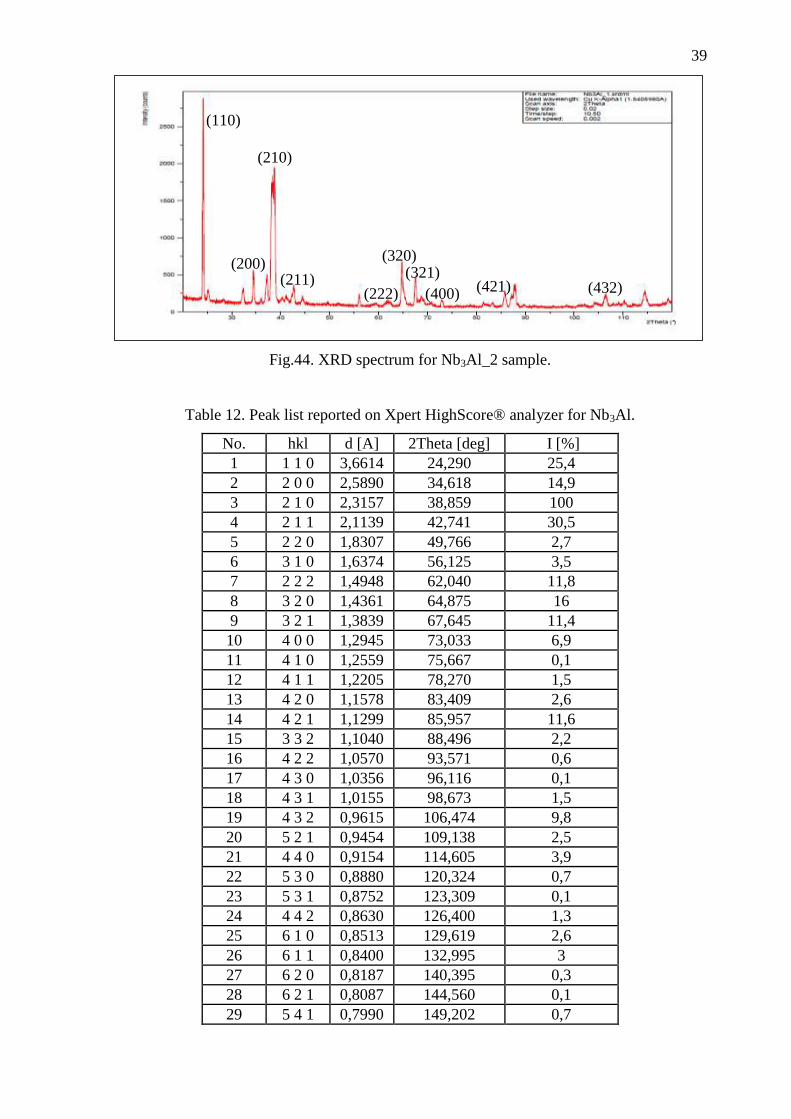
Fig.44. XRD spectrum for Nb3Al_2 sample.
Table 12. Peak list reported on Xpert HighScore® analyzer for Nb3Al.
No. hkl d [A] 2Theta [deg] I [%]
1 1 1 0 3,6614 24,290 25,4
2 2 0 0 2,5890 34,618 14,9
3 2 1 0 2,3157 38,859 100
4 2 1 1 2,1139 42,741 30,5
5 2 2 0 1,8307 49,766 2,7
6 3 1 0 1,6374 56,125 3,5
7 2 2 2 1,4948 62,040 11,8
8 3 2 0 1,4361 64,875 16
9 3 2 1 1,3839 67,645 11,4
10 4 0 0 1,2945 73,033 6,9
11 4 1 0 1,2559 75,667 0,1
12 4 1 1 1,2205 78,270 1,5
13 4 2 0 1,1578 83,409 2,6
14 4 2 1 1,1299 85,957 11,6
15 3 3 2 1,1040 88,496 2,2
16 4 2 2 1,0570 93,571 0,6
17 4 3 0 1,0356 96,116 0,1
18 4 3 1 1,0155 98,673 1,5
19 4 3 2 0,9615 106,474 9,8
20 5 2 1 0,9454 109,138 2,5
21 4 4 0 0,9154 114,605 3,9
22 5 3 0 0,8880 120,324 0,7
23 5 3 1 0,8752 123,309 0,1
24 4 4 2 0,8630 126,400 1,3
25 6 1 0 0,8513 129,619 2,6
26 6 1 1 0,8400 132,995 3
27 6 2 0 0,8187 140,395 0,3
28 6 2 1 0,8087 144,560 0,1
29 5 4 1 0,7990 149,202 0,7
(110)
(210)
(320) (200)
(211) (222)
(321) (421)
(400) (432)
40
The Xpert HighScore® analyzer indicates that the main diffraction planes match
with the reported for Nb3Al compound. The lattice parameter obtained from this
measurement was 5,1971 Å and the standard value is 5,1780 Å. This means that probably
this sample has low range ordering in the crystal structure i.e. low value of “S”, increasing
the distortion in the unit cell and the lattice parameter.
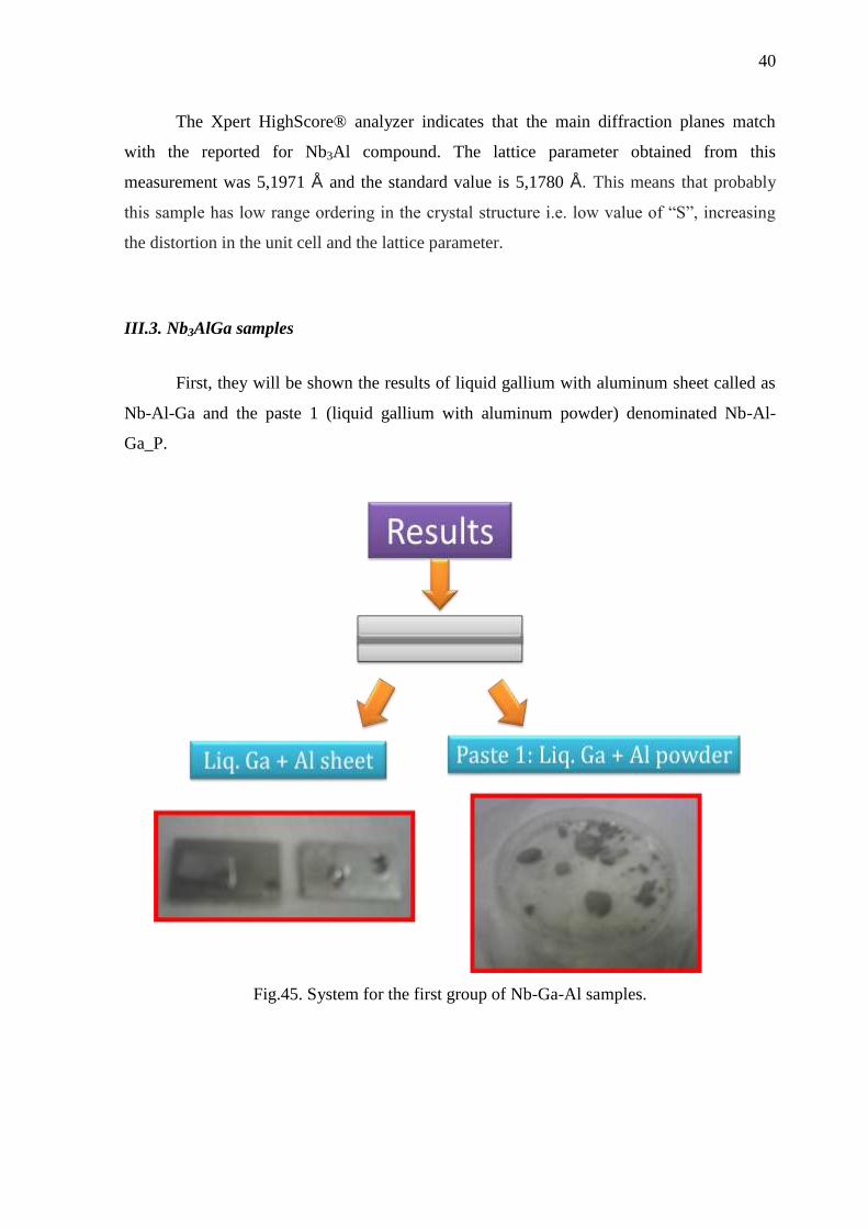
III.3. Nb3AlGa samples
First, they will be shown the results of liquid gallium with aluminum sheet called as
Nb-Al-Ga and the paste 1 (liquid gallium with aluminum powder) denominated Nb-Al-
Ga_P.
Fig.45. System for the first group of Nb-Ga-Al samples.

41
Fig.46. Phase shift vs. temperature with important transition for Nb-Al-Ga system (first
group).
Fig.47. Phase shift vs. temperature for Nb-Al-Ga system with the presence of only niobium
transition (first group).
After analyzing the figure 46 and 47, the values of critical temperatures was
calculated for each sample with its corresponding Tc.
0
0,2
0,4
0,6
0,8
1
8 9 10 11 12 13 14 15 16 17 18 19
Ph
S
Temperature [K]
Nb-Ga-Al_1
Nb-Ga-Al_2
Nb-Ga-Al_3
Nb-Ga-Al_6
Nb-Ga-Al_7
Nb-Ga-Al_P1
Nb-Ga-Al_P2
Nb-Ga-Al_P3
0
0,2
0,4
0,6
0,8
1
5 6 7 8 9 10 11 12 13 14 15 16 17 18 19 20
Ph
S
Temperature [K]
Nb-Ga-Al_4
Nb-Ga-Al_5
Nb-Ga-Al_8
42
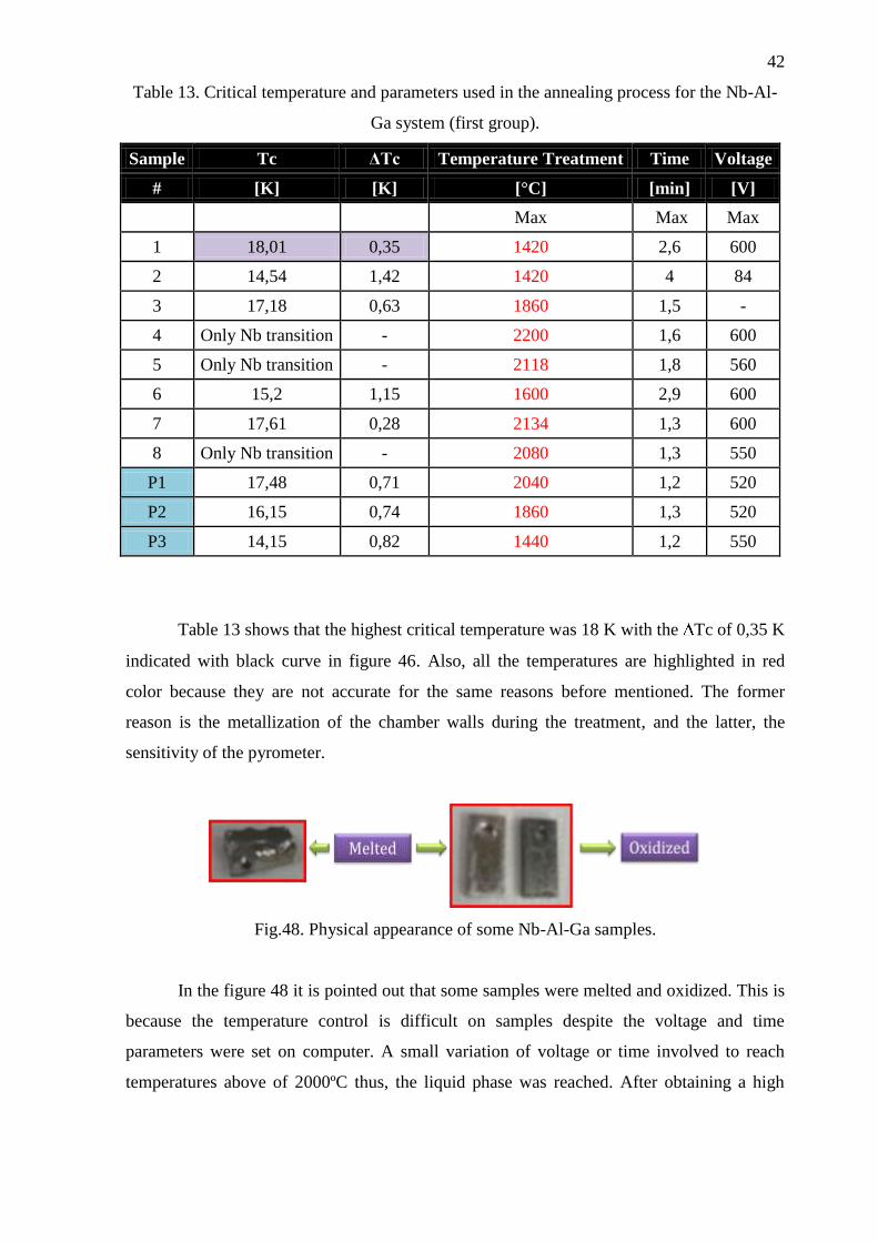
Table 13. Critical temperature and parameters used in the annealing process for the Nb-Al-
Ga system (first group).
Sample Tc ΔTc Temperature Treatment Time Voltage
# [K] [K] [°C] [min] [V]
Max Max Max
1 18,01 0,35 1420 2,6 600
2 14,54 1,42 1420 4 84
3 17,18 0,63 1860 1,5 -
4 Only Nb transition - 2200 1,6 600
5 Only Nb transition - 2118 1,8 560
6 15,2 1,15 1600 2,9 600
7 17,61 0,28 2134 1,3 600
8 Only Nb transition - 2080 1,3 550
P1 17,48 0,71 2040 1,2 520
P2 16,15 0,74 1860 1,3 520
P3 14,15 0,82 1440 1,2 550
Table 13 shows that the highest critical temperature was 18 K with the Tc of 0,35 K
indicated with black curve in figure 46. Also, all the temperatures are highlighted in red
color because they are not accurate for the same reasons before mentioned. The former
reason is the metallization of the chamber walls during the treatment, and the latter, the
sensitivity of the pyrometer.
Fig.48. Physical appearance of some Nb-Al-Ga samples.
In the figure 48 it is pointed out that some samples were melted and oxidized. This is
because the temperature control is difficult on samples despite the voltage and time
parameters were set on computer. A small variation of voltage or time involved to reach
temperatures above of 2000ºC thus, the liquid phase was reached. After obtaining a high
43
critical temperature in one sample, trying to change a little the voltage or time, three things
happen:
1) The sample is melted.
2) The critical temperature value decreases.
3) It is not present a superconducting phase.
As for the oxidation process was continually reinforced the sealing system of the
chamber in order to avoid this problem.
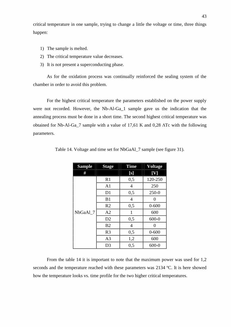
For the highest critical temperature the parameters established on the power supply
were not recorded. However, the Nb-Al-Ga_1 sample gave us the indication that the
annealing process must be done in a short time. The second highest critical temperature was
obtained for Nb-Al-Ga_7 sample with a value of 17,61 K and 0,28 Tc with the following
parameters.
Table 14. Voltage and time set for NbGaAl_7 sample (see figure 31).
Sample Stage Time Voltage
# [s] [V]
NbGaAl_7
R1 0,5 120-250
A1 4 250
D1 0,5 250-0
B1 4 0
R2 0,5 0-600
A2 1 600
D2 0,5 600-0
B2 4 0
R3 0,5 0-600
A3 1,2 600
D3 0,5 600-0
From the table 14 it is important to note that the maximum power was used for 1,2
seconds and the temperature reached with these parameters was 2134 ºC. It is here showed
how the temperature looks vs. time profile for the two higher critical temperatures.

44
Fig.49. Temperature and time profile for Nb-Ga-Al samples 1 and 7.
The parameters set for the other samples and the temperature - time profiles are
presented in the annexes. In a second opportunity, the post- annealing was conducted in
order to enhance the critical temperature. Unlike last time, it was done with the induction
system without using UHV system.
Fig.50. Effect of the post-annealing.
Table 15. Parameters used in post- annealing process.
Sample Tc ΔTc Temperature Time Voltage
# [K] [K] [°C] [min] [V]
P3_base 14,15 0,82 1440 1,2 550
P3_post1 13,81 0,91 700 60 81
P3_post2 14,24 0,67 800 60 93
P3_post3 14,36 1,12 800 60 93
P3_post4 14,67 1,1 800 60 93
0
500
1000
1500
2000
0 50 100 150
Tem
pe
ratu
re [
ºC]
Time [s]
NbGaAl_1
NbGaAl_7
0
0,2
0,4
0,6
0,8
1
8 9 10 11 12 13 14 15 16 17
Ph
S
T [K]
Nb-Ga-Al_P3
P3_post-1
P3_post-2
P3_post-3
P3_post-4
45
From figure 50 and table 15, it is observed that initial critical temperature decreases
and then increases but subtly, so the changes are not expected and even they can be
considered negligible. These can be caused by several reasons:
1) Oxidation problem because the system used was the induction heating and this fact is
worse when the annealing is performed for long time. Actually, the sample changes
to dark color.
2) Nb, Al, Ga percentages are farther away from the desired stoichiometry lower the
effect of post-annealing.
3) The annealing time was not sufficient to promote the long range ordering.
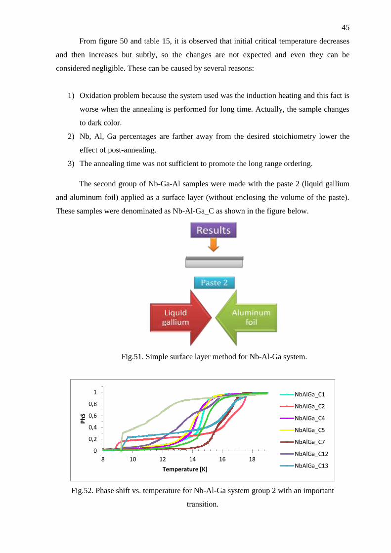
The second group of Nb-Ga-Al samples were made with the paste 2 (liquid gallium
and aluminum foil) applied as a surface layer (without enclosing the volume of the paste).
These samples were denominated as Nb-Al-Ga_C as shown in the figure below.
Fig.51. Simple surface layer method for Nb-Al-Ga system.
Fig.52. Phase shift vs. temperature for Nb-Al-Ga system group 2 with an important
transition.
0
0,2
0,4
0,6
0,8
1
8 10 12 14 16 18
Ph
S
Temperature [K]
NbAlGa_C1
NbAlGa_C2
NbAlGa_C4
NbAlGa_C5
NbAlGa_C7
NbAlGa_C12
NbAlGa_C13

46
Fig.53. Phase shift vs. temperature for Nb-Al-Ga system group 2 with only niobium
transition.
The following table shows the respective values of Tc, Tc and the parameters used.
Table 16. Critical temperature, Tc and parameters used for second group Nb-Al-Ga
system.
Sample Tc ΔTc Temperature Treatment Time Voltage
# [K] [K] [°C] [min] [V]
C1 14,86 0,75 - - 550
C2 16,71 0,84 - - 550
C3 Only Nb transition - - - 550
C4 14,16 1,22 - - 550
C5 13,96 1,29 - - 550
C6 Only Nb transition - 1838 0,9 580
C7 15,88 1,39 - - 580
C8 Only Nb transition - 2060 1,2 600
C9 Only Nb transition - 1860 1,2 550
C10 Only Nb transition - 2137 1,1 500
C11 Only Nb transition - 1827 0,4 500
C12 13,74 2,14 1640 0,5 50
C13 16,56 1,37 1860 0,7 500
C14 Only Nb transition - 1138 0,3 500
C15 11,77 1,9 1224 0,3 570
C16 15,57 1,26 1842 0,5 580
0
0,2
0,4
0,6
0,8
1
8 10 12 14 16 18
Ph
S
Temperature [K]
NbAlGa_C3
NbAlGa_C6
NbAlGa_C8
NbAlGa_C9
NbAlGa_C10
NbAlGa_C11
NbAlGa_C14
47
From figure 52 and table 16 it can be observed that the highest critical temperature
was found for Nb-Al-Ga_C2 sample with 16,71 K and Tc 0,84. Although this value is good for
the final goal (superconducting cavities), but the fact that the paste volume was not enclosed
between niobium pieces implied big amounts of paste evaporated, bringing as a result an error in
the temperature measurement and no control on the stoichiometry. For this reason, the procedure
for preparing the paste according to the composition ratio was not done with a rigid procedure.
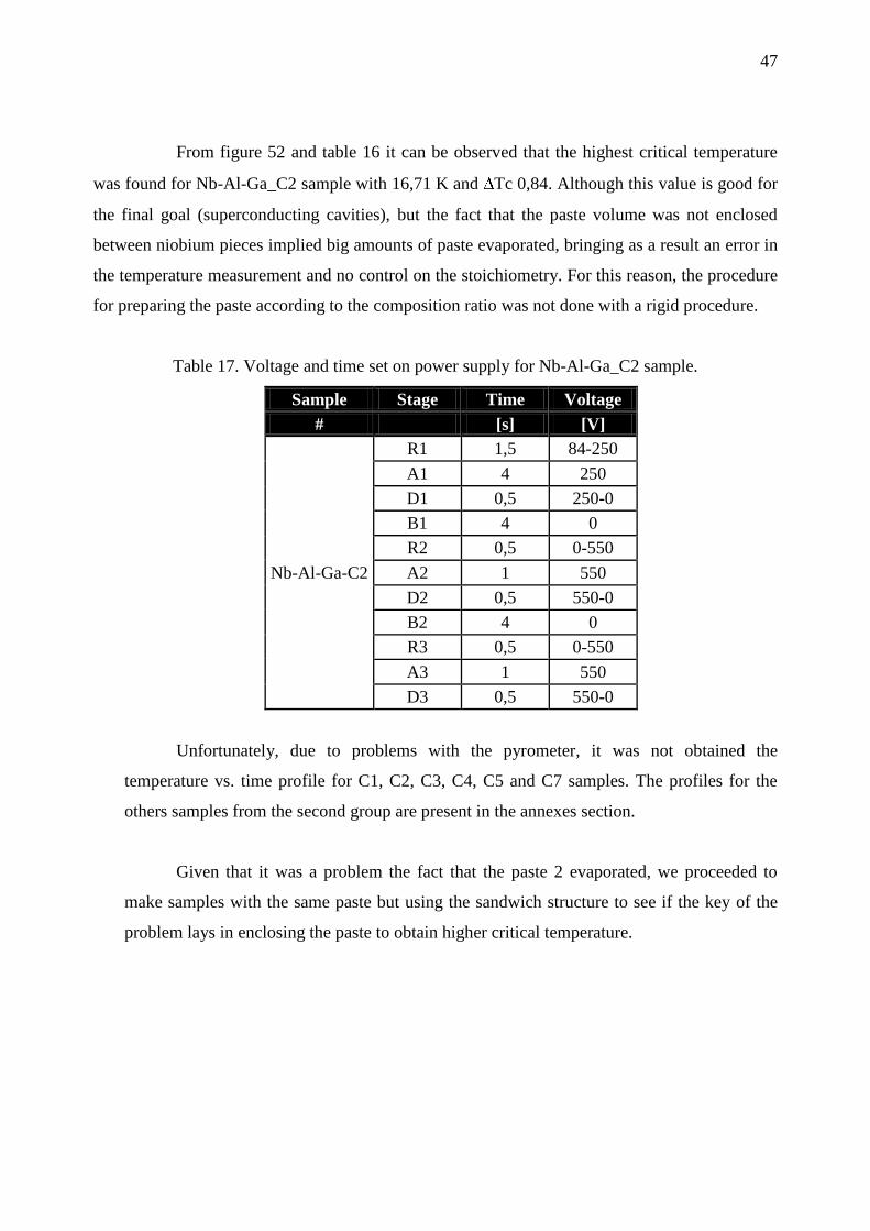
Table 17. Voltage and time set on power supply for Nb-Al-Ga_C2 sample.
Sample Stage Time Voltage
# [s] [V]
Nb-Al-Ga-C2
R1 1,5 84-250
A1 4 250
D1 0,5 250-0
B1 4 0
R2 0,5 0-550
A2 1 550
D2 0,5 550-0
B2 4 0
R3 0,5 0-550
A3 1 550
D3 0,5 550-0
Unfortunately, due to problems with the pyrometer, it was not obtained the
temperature vs. time profile for C1, C2, C3, C4, C5 and C7 samples. The profiles for the
others samples from the second group are present in the annexes section.
Given that it was a problem the fact that the paste 2 evaporated, we proceeded to
make samples with the same paste but using the sandwich structure to see if the key of the
problem lays in enclosing the paste to obtain higher critical temperature.
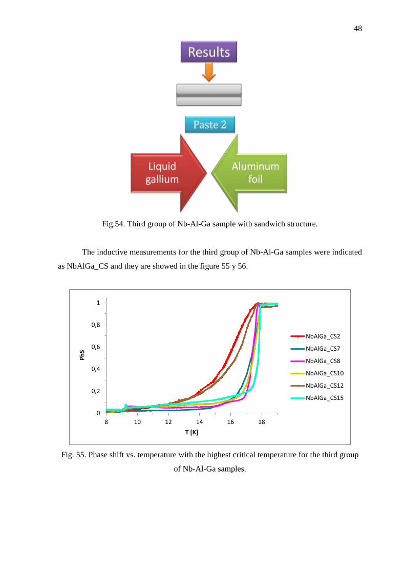
48
Fig.54. Third group of Nb-Al-Ga sample with sandwich structure.
The inductive measurements for the third group of Nb-Al-Ga samples were indicated
as NbAlGa_CS and they are showed in the figure 55 y 56.
Fig. 55. Phase shift vs. temperature with the highest critical temperature for the third group
of Nb-Al-Ga samples.
0
0,2
0,4
0,6
0,8
1
8 10 12 14 16 18
Ph
S
T [K]
NbAlGa_CS2
NbAlGa_CS7
NbAlGa_CS8
NbAlGa_CS10
NbAlGa_CS12
NbAlGa_CS15
49
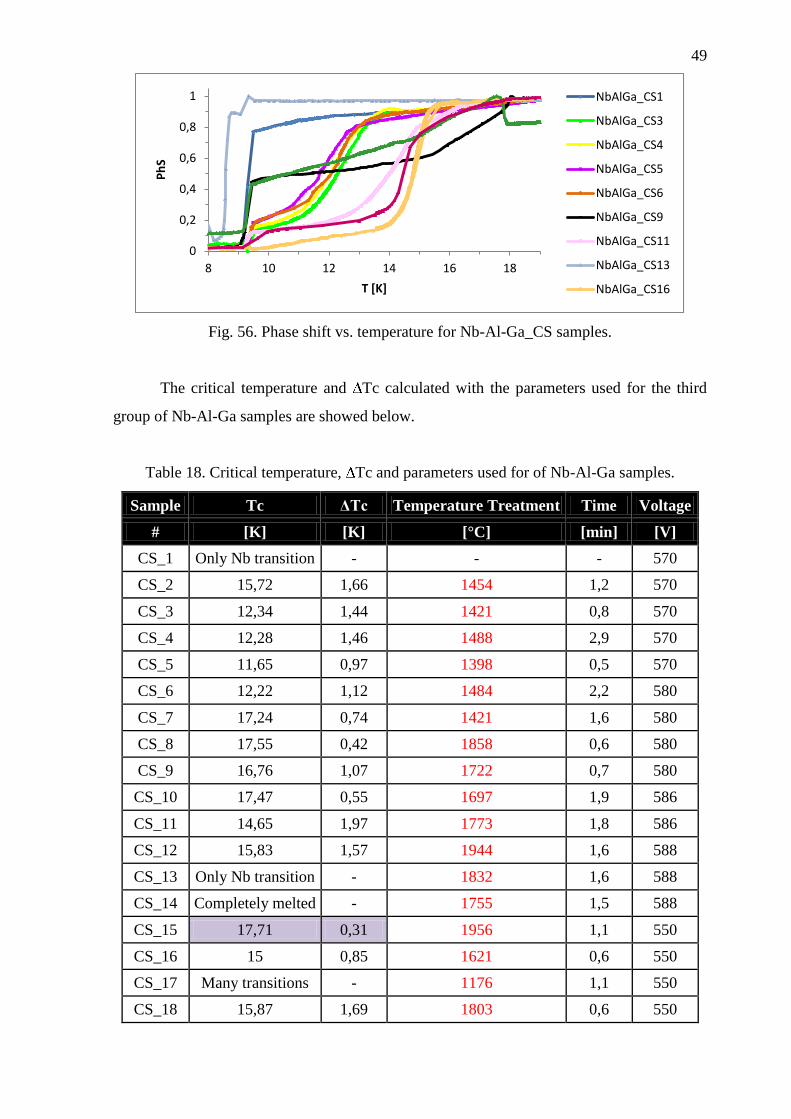
Fig. 56. Phase shift vs. temperature for Nb-Al-Ga_CS samples.
The critical temperature and Tc calculated with the parameters used for the third
group of Nb-Al-Ga samples are showed below.
Table 18. Critical temperature, Tc and parameters used for of Nb-Al-Ga samples.
Sample Tc ΔTc Temperature Treatment Time Voltage
# [K] [K] [°C] [min] [V]
CS_1 Only Nb transition - - - 570
CS_2 15,72 1,66 1454 1,2 570
CS_3 12,34 1,44 1421 0,8 570
CS_4 12,28 1,46 1488 2,9 570
CS_5 11,65 0,97 1398 0,5 570
CS_6 12,22 1,12 1484 2,2 580
CS_7 17,24 0,74 1421 1,6 580
CS_8 17,55 0,42 1858 0,6 580
CS_9 16,76 1,07 1722 0,7 580
CS_10 17,47 0,55 1697 1,9 586
CS_11 14,65 1,97 1773 1,8 586
CS_12 15,83 1,57 1944 1,6 588
CS_13 Only Nb transition - 1832 1,6 588
CS_14 Completely melted - 1755 1,5 588
CS_15 17,71 0,31 1956 1,1 550
CS_16 15 0,85 1621 0,6 550
CS_17 Many transitions - 1176 1,1 550
CS_18 15,87 1,69 1803 0,6 550
0
0,2
0,4
0,6
0,8
1
8 10 12 14 16 18
Ph
S
T [K]
NbAlGa_CS1
NbAlGa_CS3
NbAlGa_CS4
NbAlGa_CS5
NbAlGa_CS6
NbAlGa_CS9
NbAlGa_CS11
NbAlGa_CS13
NbAlGa_CS16

50
Figure 55 and table 18 shows that the highest critical temperature it was obtained for
CS15 sample, highlighted with blue color with a Tc of 17,71 K and Tc 0,31. This means
that the transition was very important because the value of Tc is high and the Tc low, so
the transition was very sharp indicated that probably the present of only one phase (A15).
These samples were performed with a maximum temperature treatment of 1950ºC and the
following profile of voltage and time.
Table 19. Voltage and time profile for CS15 sample.
Sample Stage Time Voltage
# [s] [V]
CS_15
R1 0,5 120-180
A1 6 180
D1 0,5 180-0
B1 3 0
R2 0,5 0-350
A2 5,5 350
D2 0,5 350-0
B2 5 0
R3 0,5 0-550
A3 1 550
D3 0,5 550-0
After set the profile above, in the following way looks the temperature and time
profile.
Fig.57. Temperature and time profile for CS15 sample.
0
300
600
900
1200
1500
1800
0 20 40 60
Tem
pe
ratu
re [
ºC]
Time [s]
NbAlGa_CS15
51
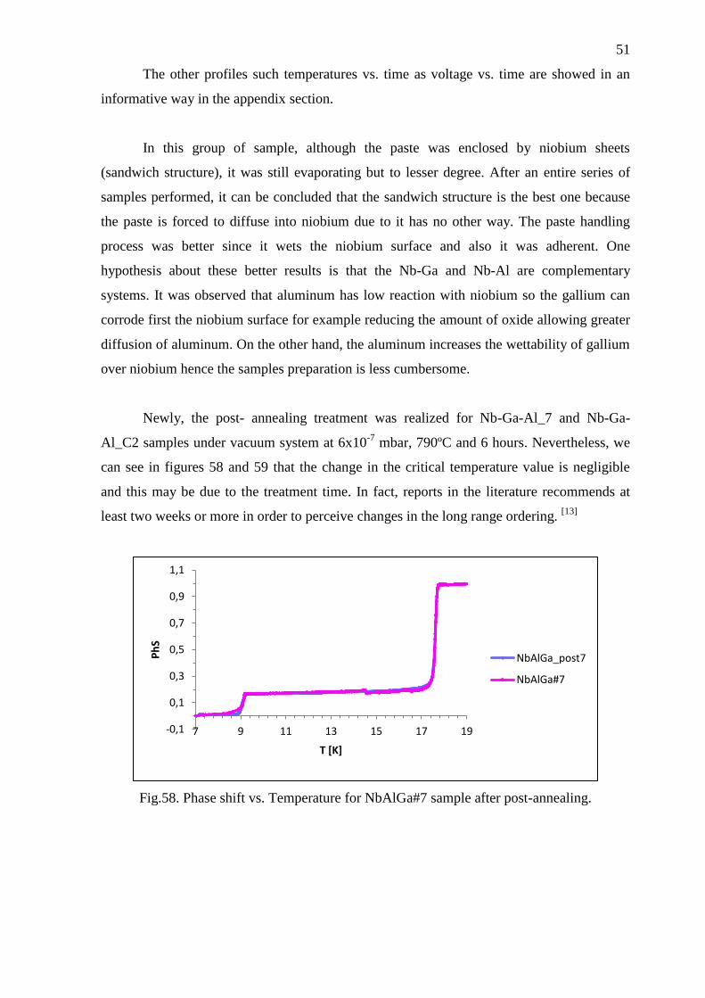
The other profiles such temperatures vs. time as voltage vs. time are showed in an
informative way in the appendix section.
In this group of sample, although the paste was enclosed by niobium sheets
(sandwich structure), it was still evaporating but to lesser degree. After an entire series of
samples performed, it can be concluded that the sandwich structure is the best one because
the paste is forced to diffuse into niobium due to it has no other way. The paste handling
process was better since it wets the niobium surface and also it was adherent. One
hypothesis about these better results is that the Nb-Ga and Nb-Al are complementary
systems. It was observed that aluminum has low reaction with niobium so the gallium can
corrode first the niobium surface for example reducing the amount of oxide allowing greater
diffusion of aluminum. On the other hand, the aluminum increases the wettability of gallium
over niobium hence the samples preparation is less cumbersome.
Newly, the post- annealing treatment was realized for Nb-Ga-Al_7 and Nb-Ga-
Al_C2 samples under vacuum system at 6x10⁻⁷
mbar, 790ºC and 6 hours. Nevertheless, we
can see in figures 58 and 59 that the change in the critical temperature value is negligible
and this may be due to the treatment time. In fact, reports in the literature recommends at
least two weeks or more in order to perceive changes in the long range ordering. [13]
Fig.58. Phase shift vs. Temperature for NbAlGa#7 sample after post-annealing.
-0,1
0,1
0,3
0,5
0,7
0,9
1,1
7 9 11 13 15 17 19
Ph
S
T [K]
NbAlGa_post7
NbAlGa#7

52
Fig.59. Phase shift vs. Temperature for NbAlGa_C2 sample after post-annealing
Nonetheless, from all the samples collected, the sample 1 of the first Nb-Al-Ga group
it was obtained the highest Tc at 18 K with Tc 0,35 which means that the transition phase
is very sharp. Thus, it was analyzed the chemical composition and morphologies by means
of Scanning Electron Microscopy (SEM) “XL-30” model produced by Philips Company
with an electron source of W filament. The interaction between electrons and the atoms of
sample make up signals that contain the following showed below.
Fig.60. Chemical composition and morphology on the red point.
0
0,2
0,4
0,6
0,8
1
8 10 12 14 16 18
Ph
S
T [K]
NbAlGa_C2_post
NbAlGa_C2
53
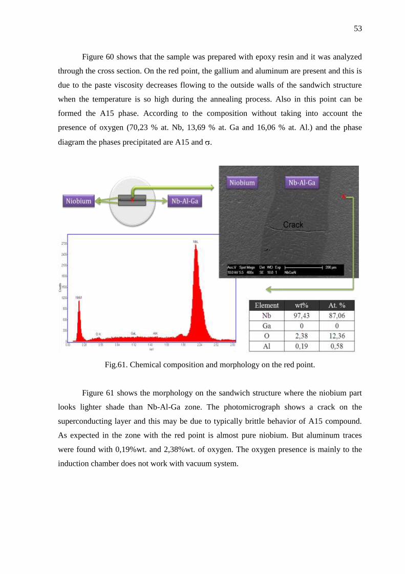
Figure 60 shows that the sample was prepared with epoxy resin and it was analyzed
through the cross section. On the red point, the gallium and aluminum are present and this is
due to the paste viscosity decreases flowing to the outside walls of the sandwich structure
when the temperature is so high during the annealing process. Also in this point can be
formed the A15 phase. According to the composition without taking into account the
presence of oxygen (70,23 % at. Nb, 13,69 % at. Ga and 16,06 % at. Al.) and the phase
diagram the phases precipitated are A15 and .
Fig.61. Chemical composition and morphology on the red point.
Figure 61 shows the morphology on the sandwich structure where the niobium part
looks lighter shade than Nb-Al-Ga zone. The photomicrograph shows a crack on the
superconducting layer and this may be due to typically brittle behavior of A15 compound.
As expected in the zone with the red point is almost pure niobium. But aluminum traces
were found with 0,19%wt. and 2,38%wt. of oxygen. The oxygen presence is mainly to the
induction chamber does not work with vacuum system.
54
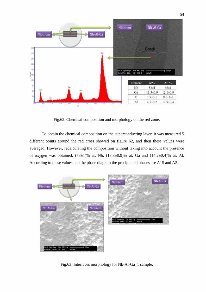
Fig.62. Chemical composition and morphology on the red zone.
To obtain the chemical composition on the superconducting layer, it was measured 5
different points around the red cross showed on figure 62, and then these values were
averaged. However, recalculating the composition without taking into account the presence
of oxygen was obtained: (73±1)% at. Nb, (13,3±0,9)% at. Ga and (14,2±0,4)% at. Al.
According to these values and the phase diagram the precipitated phases are A15 and A2.
Fig.63. Interfaces morphology for Nb-Al-Ga_1 sample.
55
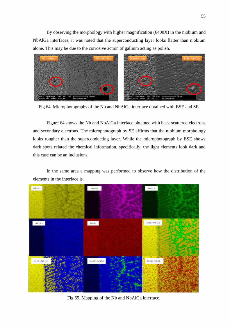
By observing the morphology with higher magnification (6400X) in the niobium and
NbAlGa interfaces, it was noted that the superconducting layer looks flatter than niobium
alone. This may be due to the corrosive action of gallium acting as polish.
Fig.64. Microphotographs of the Nb and NbAlGa interface obtained with BSE and SE.
Figure 64 shows the Nb and NbAlGa interface obtained with back scattered electrons
and secondary electrons. The microphotograph by SE affirms that the niobium morphology
looks rougher than the superconducting layer. While the microphotograph by BSE shows
dark spots related the chemical information, specifically, the light elements look dark and
this case can be an inclusions.
In the same area a mapping was performed to observe how the distribution of the
elements in the interface is.
Fig.65. Mapping of the Nb and NbAlGa interface.

56
According to the following table, the brighter pixel of the mapping corresponds to
the higher X-rays counts. Thus, it indicates that gallium diffuses in such way that creates
channels and this behavior is due to its corrosive property. The aluminum diffuses uniformly
but the brighter pixel is also located is the same place that brighter place of gallium. This
means that the gallium helps to aluminum in the diffusive process. The oxygen is completely
uniform and combinations of these elements were represented such as Ga-Nb, Al-Nb, Ga-Al
and O-Nb.
Table 20. X- ray counts obtained from mapping measurement.
Total Counts X-Rays
Element Color Smin Smax
O K Red 11 99
Ga L Green 17 405
Al K Blue 19 296
Nb L Yellow 151 2805
Ga K Purple 21 366
XRD analysis was not performed for Nb-Al-Ga_1 sample because the sandwich
structure would not allow it and also it could not open because this was embedded in epoxy
resin.
III.4. Cavities
After making a long study on samples and knowing that it is possible to obtain good
superconducting layer preferentially on NbAlGa system, we began to do preliminary testing
of 6GHz niobium cavities. The results were the following.
Fig.66. Results of the tests with the cavities.
57
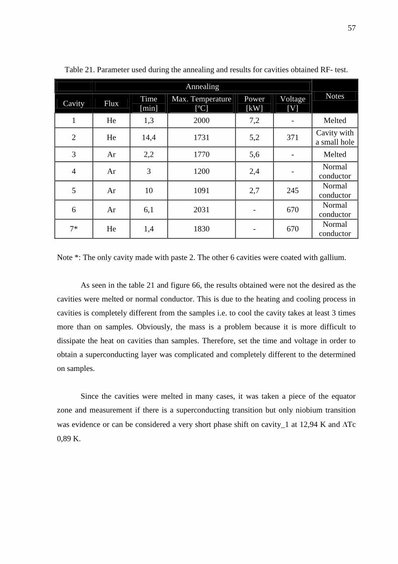
Table 21. Parameter used during the annealing and results for cavities obtained RF- test.
Annealing
Notes Cavity Flux
Time
[min]
Max. Temperature
[ºC]
Power
[kW]
Voltage
[V]
1 He 1,3 2000 7,2 - Melted
2 He 14,4 1731 5,2 371 Cavity with
a small hole
3 Ar 2,2 1770 5,6 - Melted
4 Ar 3 1200 2,4 - Normal
conductor
5 Ar 10 1091 2,7 245 Normal
conductor
6 Ar 6,1 2031 - 670 Normal
conductor
7* He 1,4 1830 - 670 Normal
conductor
Note *: The only cavity made with paste 2. The other 6 cavities were coated with gallium.
As seen in the table 21 and figure 66, the results obtained were not the desired as the
cavities were melted or normal conductor. This is due to the heating and cooling process in
cavities is completely different from the samples i.e. to cool the cavity takes at least 3 times
more than on samples. Obviously, the mass is a problem because it is more difficult to
dissipate the heat on cavities than samples. Therefore, set the time and voltage in order to
obtain a superconducting layer was complicated and completely different to the determined
on samples.
Since the cavities were melted in many cases, it was taken a piece of the equator
zone and measurement if there is a superconducting transition but only niobium transition
was evidence or can be considered a very short phase shift on cavity_1 at 12,94 K and Tc
0,89 K.

58
Fig.67. Phase shift vs. temperature for cavities 1, 2 and 3.
The parameters recorded and the temperature - time profile are shown below.
Table 22. Voltage and time parameter for cavities 6 and 7.
Cavities Stage Time Voltage
# [s] [V]
6 and 7
R1 1,5 91-450
A1 30 450
D1 - -
B1 - -
R2 1,5 450-670
A2 5 670
D2 0,5 670-500
B2 3 500
R3 0,5 500-650
A3 3 650
D3 0 650-0
0
0,1
0,2
0,3
0,4
0,5
0,6
0,7
0,8
0,9
1
6 7 8 9 10 11 12 13 14 15
Ph
S
T [K]
Cavity 1_Nb3Ga
Cavity2_Nb3Ga
Cavity3_Nb3Ga
59
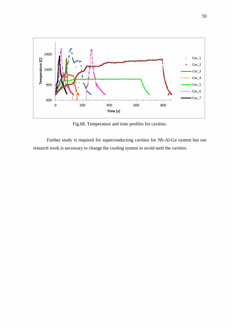
Fig.68. Temperature and time profiles for cavities.
Further study is required for superconducting cavities for Nb-Al-Ga system but our
research work is necessary to change the cooling system to avoid melt the cavities.
400
900
1400
1900
0 200 400 600 800
Tem
pe
ratu
re [
C]
Time [s]
Cav_1
Cav_2
Cav_3
Cav_4
Cav_5
Cav_6
Cav_7
60
CHAPTER 4. CONCLUSIONS
On the present work was implemented a methodology to obtain Nb3AlGa compound
for samples by means of induction heating, but unfortunately further studies are necessary to
obtain Nb3AlGa coating on 6GHz cavities.
The Nb-Ga and Nb-Al system are complementary because the aluminum improves
the wettability of the gallium over niobium, while the gallium corrodes the surface of
niobium, improving the diffusion of aluminum.
The gallium acts as polish solution according to microphotographs obtained by SEM
measurements making flatter the superconducting layer in comparison with bulk niobium
sample.
The temperature measurement is very sensitive to changes in time (milliseconds)
and voltage. Also, errors on temperature are reported due to the metallization chamber walls
and sensibility of the pyrometer.
Reproducibility problems by induction heating system are present as at the same
parameters on voltage and time different critical temperatures were found.
Enclose the volume of the paste 2 is the key of the treatment to decrease the amount
of gallium and aluminum evaporated as force the diffusion of the elements within niobium.
Also, short times for annealing by induction are necessary to precipitate the superconducting
A15 phase. That means we need a closed configuration indeed the best samples were those
performed in a niobium sandwich configuration.
Samples with a heat treatment below to 1500°C do not present a superconducting
transition and if it is obtained the critical temperature is around 12 and 13 K. While, when
the temperature of annealing was between 1500 and 1900 °C the phase shift was obtained
between 14 and 18 K.
Finally, despite it was posed a methodology, it can be improved by the
recommendations outlined below.

61
CHAPTER 5. RECOMMENDATIONS
For future experiments by means of induction heating it is necessary to consider a
better cooling system for cavities in order to enhance the control on the cooling system.
Better control of the niobium-aluminum-gallium stoichiometry.
Fix all the possible parameters such as: sample position into the chamber, sample
mass, flux, gas purity and contaminations to obtain reproducible results.
Perform the post-annealing on samples for long time, more than 2 weeks, in vacuum
system to improve the long range ordering.

62
CHAPTER 6. BIBLIOGRAPHY
1 Hasan Padamsee, “The science and technology of superconducting cavities for
accelerators”, Supercond.Sci. Technol., 14 (2001) R28–R51.
2 A. Chao, H. Moser, Z. Zhao. “Accelerator Physics, Technology and Applications”, World
Scientific Publishing, 2004, USA.
3 S. Turner. “Superconductivity in Particles Accelerators”. CERN Accelerator School.
(1996).
4 R. Russenschuck, G. Vandoni. “ Superconductivity and Cryogenics for accelerators and
detectors”. CERN Accelerator School. (2004).
5 B. Aune et al., "Superconducting TESLA cavities", Phys. Rev. ST Accel. Beams 3, 092001
(2000).
6 P. C. Poole. “Handbook of Superconductivity”, Academic Press. 2000. USA.
7 V. Palmieri, “New materials for superconducting radiofrequency cavities”, LNL_INFN.
Italy.
8 A. K. Saxena. “High Temperature Superconductors”, Springer. 2010. New York.
9 V. Palmieri, “The Classical Superconductivity: Phenomenology of low temperature
superconductors”, European training on technologies and industrial application of
superconductivity, LNL_INFN, (1992) 1-34.
10 C. Poole, H. Farach, “Superconductivity” Second Edition. Elsevier. 77. (2007). USA.
11 P. C. Poole. “Handbook of Superconductivity”, Academic Press. 2000. USA.

63
12 R. Flukiger, J. Jorda. “The effects of composition and atomic ordering on
superconductivity in the systems Nb3Ga and V3Ga”. Solid State Communications, Vol. 22.
(1977) 109-112. Switzerland.
13 K. Inoue, A. Kikuchi, Y. Yoshida, Y. Iijima. “A new practical superconductor: rapidly
heated and quenched Nb3Ga wire”. Physica C 384. (2003) 267-273. Japan.
14 G. W. Webb. “Niobium- Gallium Superconductor”.United States Patent 3801378. (1974)
New York.
15 G.W. Webb, L.J. Vieland, R.E Miller, A. Wicklund. “Superconductivity above 20 K in
stoichiometric Nb3Ga”. Solid State Communications, Vol. 9. (1971) 1769-1773. New York.
16 M. Hong. “Direct solid-state precipitation processed A15 (Nb3Al) superconducting
material” Lawrence Berkeley National Laboratory. (1980). California.
17 J.L. Jorda, R. Flükiger, J. Muller. “A New metallurgical investigation of the niobium-
aluminum system” Journal of the Less Common Metals. Volume 75, Issue 2. 227–239.
(1980) Switzerland.
18 A. Kikuchi, Y. Yoshida, Y. Iijima, K. Inoue. “Microstructures and superconducying
properties of transformed Nb3Al wire”. Physica C 372-376. (2002) 1307-1310. Japan.
19 N. Banno, T. Takeuchi, T. Fukuzaki, H. Wada. “Optimization of the TRUQ method for
Nb3Al superconductors”. Supercond. Sci. Technol. 15. (2002) 519-525. Japan.
20 M. Drys. “The niobium-aluminium-gallium system I. Phase equilibria at 1000 ºC”.
Journal of the Less-Common Metals, 44 (1976) 229 – 233. Poland.
21 M. Drys, N. Iliew. “The niobium-aluminium-gallium system II. Superconducting
transition temperatures” Journal of the Less-Common Metals, 44 (1976) 235 – 238. Poland.
64
ANNEXES
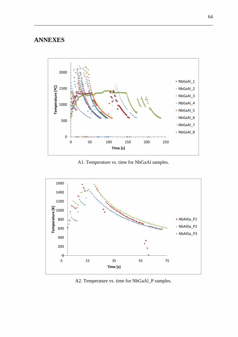
A1. Temperature vs. time for NbGaAl samples.
A2. Temperature vs. time for NbGaAl_P samples.
0
500
1000
1500
2000
0 50 100 150 200 250
Tem
pe
ratu
re [
ºC]
Time [s]
NbGaAl_1
NbGaAl_2
NbGaAl_3
NbGaAl_4
NbGaAl_5
NbGaAl_6
NbGaAl_7
NbGaAl_8
0
200
400
600
800
1000
1200
1400
1600
-5 15 35 55 75
Tem
pe
ratu
re [
K]
Time [s]
NbAlGa_P1
NbAlGa_P2
NbAlGa_P3
65
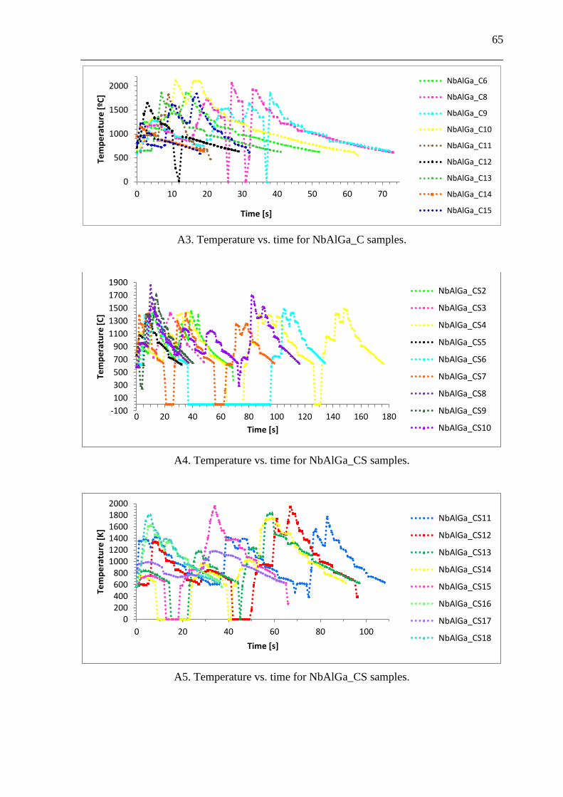
A3. Temperature vs. time for NbAlGa_C samples.
A4. Temperature vs. time for NbAlGa_CS samples.
A5. Temperature vs. time for NbAlGa_CS samples.
0
500
1000
1500
2000
0 10 20 30 40 50 60 70
Tem
pe
ratu
re [
ºC]
Time [s]
NbAlGa_C6
NbAlGa_C8
NbAlGa_C9
NbAlGa_C10
NbAlGa_C11
NbAlGa_C12
NbAlGa_C13
NbAlGa_C14
NbAlGa_C15
-100
100
300
500
700
900
1100
1300
1500
1700
1900
0 20 40 60 80 100 120 140 160 180
Tem
pe
ratu
re [
C]
Time [s]
NbAlGa_CS2
NbAlGa_CS3
NbAlGa_CS4
NbAlGa_CS5
NbAlGa_CS6
NbAlGa_CS7
NbAlGa_CS8
NbAlGa_CS9
NbAlGa_CS10
0 200 400 600 800
1000 1200 1400 1600 1800 2000
0 20 40 60 80 100
Tem
pe
ratu
re [
K]
Time [s]
NbAlGa_CS11
NbAlGa_CS12
NbAlGa_CS13
NbAlGa_CS14
NbAlGa_CS15
NbAlGa_CS16
NbAlGa_CS17
NbAlGa_CS18
66
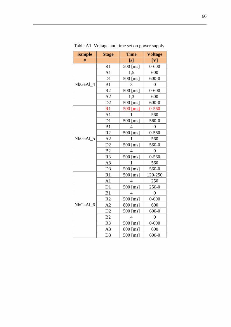
Table A1. Voltage and time set on power supply.
Sample Stage Time Voltage
# [s] [V]
NbGaAl_4
R1 500 [ms] 0-600
A1 1,5 600
D1 500 [ms] 600-0
B1 3 0
R2 500 [ms] 0-600
A2 1,3 600
D2 500 [ms] 600-0
NbGaAl_5
R1 500 [ms] 0-560
A1 1 560
D1 500 [ms] 560-0
B1 4 0
R2 500 [ms] 0-560
A2 1 560
D2 500 [ms] 560-0
B2 4 0
R3 500 [ms] 0-560
A3 1 560
D3 500 [ms] 560-0
NbGaAl_6
R1 500 [ms] 120-250
A1 4 250
D1 500 [ms] 250-0
B1 4 0
R2 500 [ms] 0-600
A2 800 [ms] 600
D2 500 [ms] 600-0
B2 4 0
R3 500 [ms] 0-600
A3 800 [ms] 600
D3 500 [ms] 600-0

67
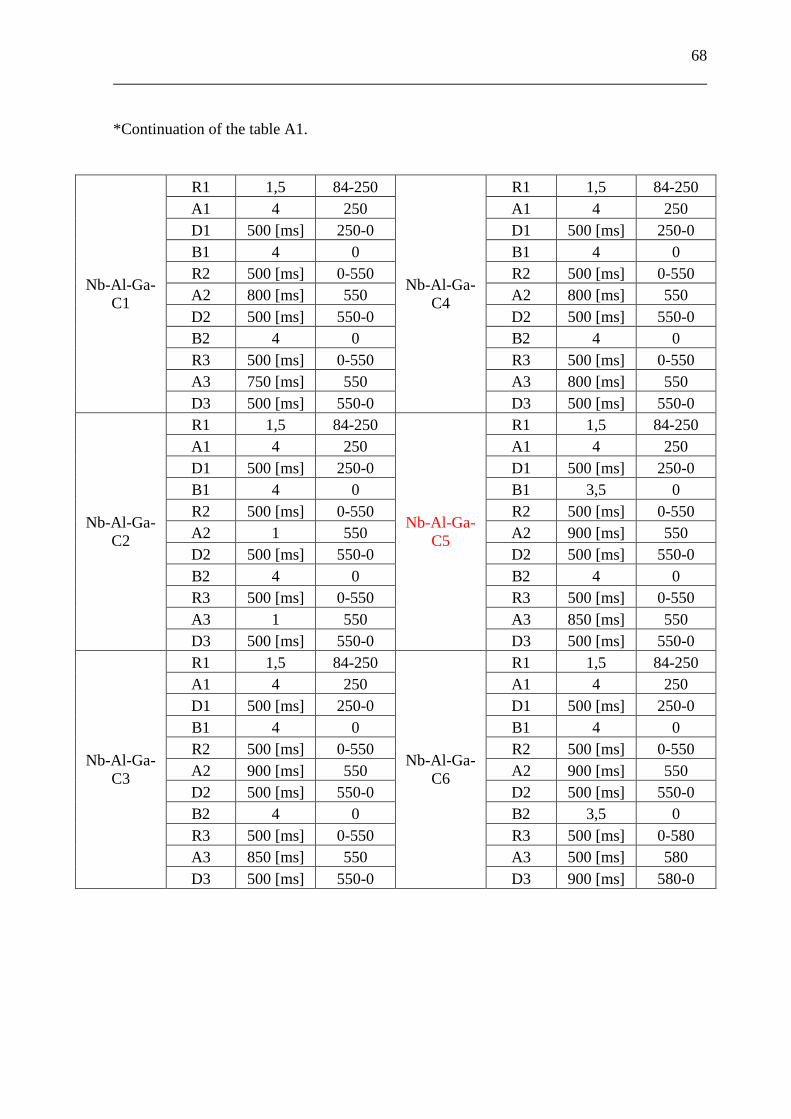
*Continuation of the table A1.
NbGaAl_7
R1 500 [ms] 120-250
Nb-Al-Ga-
P1
R1 2 84-250
A1 4 250 A1 4 250
D1 500 [ms] 250-0 D1 500 [ms] 250-0
B1 4 0 B1 4 0
R2 500 [ms] 0-600 R2 500 [ms] 0-520
A2 1 600 A2 1 520
D2 500 [ms] 600-0 D2 500 [ms] 520-0
B2 4 0 B2 4 0
R3 500 [ms] 0-600 R3 500 [ms] 0-520
A3 1,2 600 A3 1,5 520
D3 500 [ms] 600-0 D3 500 [ms] 520-0
NbGaAl_8
R1 500 [ms] 84-250
Nb-Al-Ga-
P2
R1 4 84-250
A1 4 250 A1 5 250
D1 500 [ms] 250-0 D1 500 [ms] 250-0
B1 4 0 B1 4 0
R2 500 [ms] 0-550 R2 500 [ms] 0-520
A2 1 550 A2 1 520
D2 500 [ms] 550-0 D2 500 [ms] 520-0
B2 4 0 B2 4 0
R3 500 [ms] 0-550 R3 500 [ms] 0-520
A3 1,5 550 A3 1,5 520
D3 500 [ms] 550-0 D3 500 [ms] 520-0
Nb-
Gawire
R1 500 [ms] 120-250
Nb-Al-Ga-
P3
R1 1,5 84-250
A1 4 250 A1 4 250
D1 500 [ms] 250-0 D1 500 [ms] 250-0
B1 4 0 B1 4 0
R2 500 [ms] 0-600 R2 500 [ms] 0-550
A2 1 600 A2 1 550
D2 500 [ms] 600-0 D2 500 [ms] 550-0
B2 4 0 B2 4 0
R3 500 [ms] 0-600 R3 500 [ms] 0-550
A3 1,5 600 A3 1,5 550
D3 500 [ms] 600-0 D3 500 [ms] 550-0
68
*Continuation of the table A1.
Nb-Al-Ga-
C1
R1 1,5 84-250
Nb-Al-Ga-
C4
R1 1,5 84-250
A1 4 250 A1 4 250
D1 500 [ms] 250-0 D1 500 [ms] 250-0
B1 4 0 B1 4 0
R2 500 [ms] 0-550 R2 500 [ms] 0-550
A2 800 [ms] 550 A2 800 [ms] 550
D2 500 [ms] 550-0 D2 500 [ms] 550-0
B2 4 0 B2 4 0
R3 500 [ms] 0-550 R3 500 [ms] 0-550
A3 750 [ms] 550 A3 800 [ms] 550
D3 500 [ms] 550-0 D3 500 [ms] 550-0
Nb-Al-Ga-
C2
R1 1,5 84-250
Nb-Al-Ga-
C5
R1 1,5 84-250
A1 4 250 A1 4 250
D1 500 [ms] 250-0 D1 500 [ms] 250-0
B1 4 0 B1 3,5 0
R2 500 [ms] 0-550 R2 500 [ms] 0-550
A2 1 550 A2 900 [ms] 550
D2 500 [ms] 550-0 D2 500 [ms] 550-0
B2 4 0 B2 4 0
R3 500 [ms] 0-550 R3 500 [ms] 0-550
A3 1 550 A3 850 [ms] 550
D3 500 [ms] 550-0 D3 500 [ms] 550-0
Nb-Al-Ga-
C3
R1 1,5 84-250
Nb-Al-Ga-
C6
R1 1,5 84-250
A1 4 250 A1 4 250
D1 500 [ms] 250-0 D1 500 [ms] 250-0
B1 4 0 B1 4 0
R2 500 [ms] 0-550 R2 500 [ms] 0-550
A2 900 [ms] 550 A2 900 [ms] 550
D2 500 [ms] 550-0 D2 500 [ms] 550-0
B2 4 0 B2 3,5 0
R3 500 [ms] 0-550 R3 500 [ms] 0-580
A3 850 [ms] 550 A3 500 [ms] 580
D3 500 [ms] 550-0 D3 900 [ms] 580-0

69
*Continuation of the table A1.
Nb-Al-Ga-
C7N
R1 1,5 84-250
Nb-Al-Ga-
C10
R1 1,5 84-250
A1 4 250 A1 5 250
D1 500 [ms] 250-0 D1 500 [ms] 250-0
B1 4 0 B1 3,5 0
R2 500 [ms] 0-550 R2 500 [ms] 0-500
A2 900 [ms] 550 A2 1,2 500
D2 500 [ms] 550-0 D2 500 [ms] 500-0
B2 3,5 0 B2 3,5 0
R3 500 [ms] 0-580 R3 500 [ms] 0-500
A3 500 [ms] 580 A3 1,2 500
D3 900 [ms] 580-0 D3 500 [ms] 500-0
Nb-Al-Ga-
C8
R1 1,5 84-250
Nb-Al-Ga-
C11
R1 1,5 84-250
A1 4 250 A1 1,5 250
D1 500 [ms] 250-0 D1 500 [ms] 250-0
B1 4 0 B1 3,5 0
R2 500 [ms] 0-550 R2 500 [ms] 0-500
A2 900 [ms] 550 A2 1,2 500
D2 500 [ms] 550-0 D2 500 [ms] 500-0
B2 3,5 0 B2 3,5 0
R3 500 [ms] 0-600 R3 500 [ms] 0-500
A3 800 [ms] 600 A3 1,2 500
D3 900 [ms] 600-0 D3 500 [ms] 500-0
Nb-Al-Ga-
C9
R1 1,5 84-250
Nb-Al-Ga-
C12
R1 1,5 84-200
A1 5 250 A1 1,5 200
D1 500 [ms] 250-0 D1 1,5 200-0
B1 3,5 0 B1 4 0
R2 500 [ms] 0-550 R2 500 [ms] 0-500
A2 1,2 550 A2 1,3 500
D2 500 [ms] 550-0 D2 250 [ms] 500-0
B2 3,5 0
R3 500 [ms] 0-500
A3 1,2 500
D3 900 [ms] 500-0
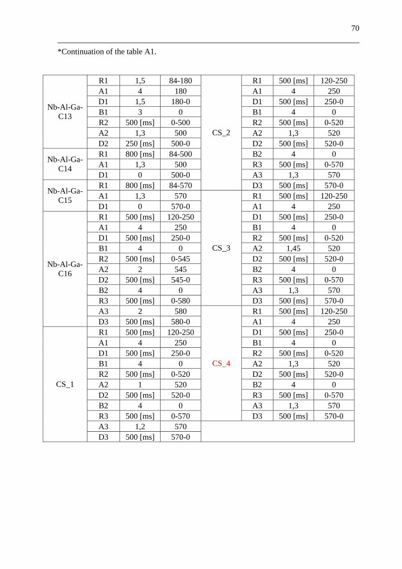
70
*Continuation of the table A1.
Nb-Al-Ga-
C13
R1 1,5 84-180
CS_2
R1 500 [ms] 120-250
A1 4 180 A1 4 250
D1 1,5 180-0 D1 500 [ms] 250-0
B1 3 0 B1 4 0
R2 500 [ms] 0-500 R2 500 [ms] 0-520
A2 1,3 500 A2 1,3 520
D2 250 [ms] 500-0 D2 500 [ms] 520-0
Nb-Al-Ga-
C14
R1 800 [ms] 84-500 B2 4 0
A1 1,3 500 R3 500 [ms] 0-570
D1 0 500-0 A3 1,3 570
Nb-Al-Ga-
C15
R1 800 [ms] 84-570 D3 500 [ms] 570-0
A1 1,3 570
CS_3
R1 500 [ms] 120-250
D1 0 570-0 A1 4 250
Nb-Al-Ga-
C16
R1 500 [ms] 120-250 D1 500 [ms] 250-0
A1 4 250 B1 4 0
D1 500 [ms] 250-0 R2 500 [ms] 0-520
B1 4 0 A2 1,45 520
R2 500 [ms] 0-545 D2 500 [ms] 520-0
A2 2 545 B2 4 0
D2 500 [ms] 545-0 R3 500 [ms] 0-570
B2 4 0 A3 1,3 570
R3 500 [ms] 0-580 D3 500 [ms] 570-0
A3 2 580
CS_4
R1 500 [ms] 120-250
D3 500 [ms] 580-0 A1 4 250
CS_1
R1 500 [ms] 120-250 D1 500 [ms] 250-0
A1 4 250 B1 4 0
D1 500 [ms] 250-0 R2 500 [ms] 0-520
B1 4 0 A2 1,3 520
R2 500 [ms] 0-520 D2 500 [ms] 520-0
A2 1 520 B2 4 0
D2 500 [ms] 520-0 R3 500 [ms] 0-570
B2 4 0 A3 1,3 570
R3 500 [ms] 0-570 D3 500 [ms] 570-0
A3 1,2 570
D3 500 [ms] 570-0
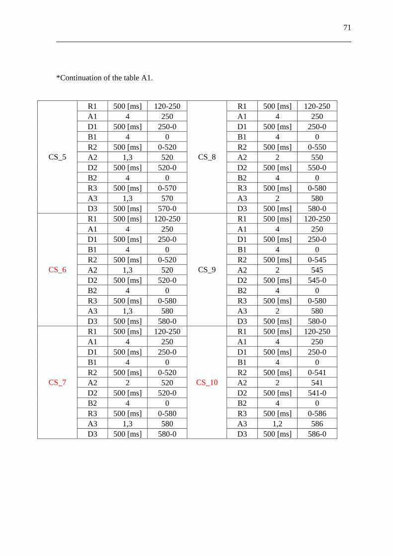
71
*Continuation of the table A1.
CS_5
R1 500 [ms] 120-250
CS_8
R1 500 [ms] 120-250
A1 4 250 A1 4 250
D1 500 [ms] 250-0 D1 500 [ms] 250-0
B1 4 0 B1 4 0
R2 500 [ms] 0-520 R2 500 [ms] 0-550
A2 1,3 520 A2 2 550
D2 500 [ms] 520-0 D2 500 [ms] 550-0
B2 4 0 B2 4 0
R3 500 [ms] 0-570 R3 500 [ms] 0-580
A3 1,3 570 A3 2 580
D3 500 [ms] 570-0 D3 500 [ms] 580-0
CS_6
R1 500 [ms] 120-250
CS_9
R1 500 [ms] 120-250
A1 4 250 A1 4 250
D1 500 [ms] 250-0 D1 500 [ms] 250-0
B1 4 0 B1 4 0
R2 500 [ms] 0-520 R2 500 [ms] 0-545
A2 1,3 520 A2 2 545
D2 500 [ms] 520-0 D2 500 [ms] 545-0
B2 4 0 B2 4 0
R3 500 [ms] 0-580 R3 500 [ms] 0-580
A3 1,3 580 A3 2 580
D3 500 [ms] 580-0 D3 500 [ms] 580-0
CS_7
R1 500 [ms] 120-250
CS_10
R1 500 [ms] 120-250
A1 4 250 A1 4 250
D1 500 [ms] 250-0 D1 500 [ms] 250-0
B1 4 0 B1 4 0
R2 500 [ms] 0-520 R2 500 [ms] 0-541
A2 2 520 A2 2 541
D2 500 [ms] 520-0 D2 500 [ms] 541-0
B2 4 0 B2 4 0
R3 500 [ms] 0-580 R3 500 [ms] 0-586
A3 1,3 580 A3 1,2 586
D3 500 [ms] 580-0 D3 500 [ms] 586-0
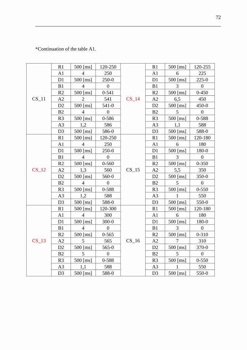
72
*Continuation of the table A1.
CS_11
R1 500 [ms] 120-250
CS_14
R1 500 [ms] 120-255
A1 4 250 A1 6 225
D1 500 [ms] 250-0 D1 500 [ms] 225-0
B1 4 0 B1 3 0
R2 500 [ms] 0-541 R2 500 [ms] 0-450
A2 2 541 A2 6,5 450
D2 500 [ms] 541-0 D2 500 [ms] 450-0
B2 4 0 B2 5 0
R3 500 [ms] 0-586 R3 500 [ms] 0-588
A3 1,2 586 A3 1,1 588
D3 500 [ms] 586-0 D3 500 [ms] 588-0
CS_12
R1 500 [ms] 120-250
CS_15
R1 500 [ms] 120-180
A1 4 250 A1 6 180
D1 500 [ms] 250-0 D1 500 [ms] 180-0
B1 4 0 B1 3 0
R2 500 [ms] 0-560 R2 500 [ms] 0-350
A2 1,3 560 A2 5,5 350
D2 500 [ms] 560-0 D2 500 [ms] 350-0
B2 4 0 B2 5 0
R3 500 [ms] 0-588 R3 500 [ms] 0-550
A3 1,2 588 A3 1 550
D3 500 [ms] 588-0 D3 500 [ms] 550-0
CS_13
R1 500 [ms] 120-300
CS_16
R1 500 [ms] 120-180
A1 4 300 A1 6 180
D1 500 [ms] 300-0 D1 500 [ms] 180-0
B1 4 0 B1 3 0
R2 500 [ms] 0-565 R2 500 [ms] 0-310
A2 5 565 A2 7 310
D2 500 [ms] 565-0 D2 500 [ms] 370-0
B2 5 0 B2 5 0
R3 500 [ms] 0-588 R3 500 [ms] 0-550
A3 1,1 588 A3 1 550
D3 500 [ms] 588-0 D3 500 [ms] 550-0
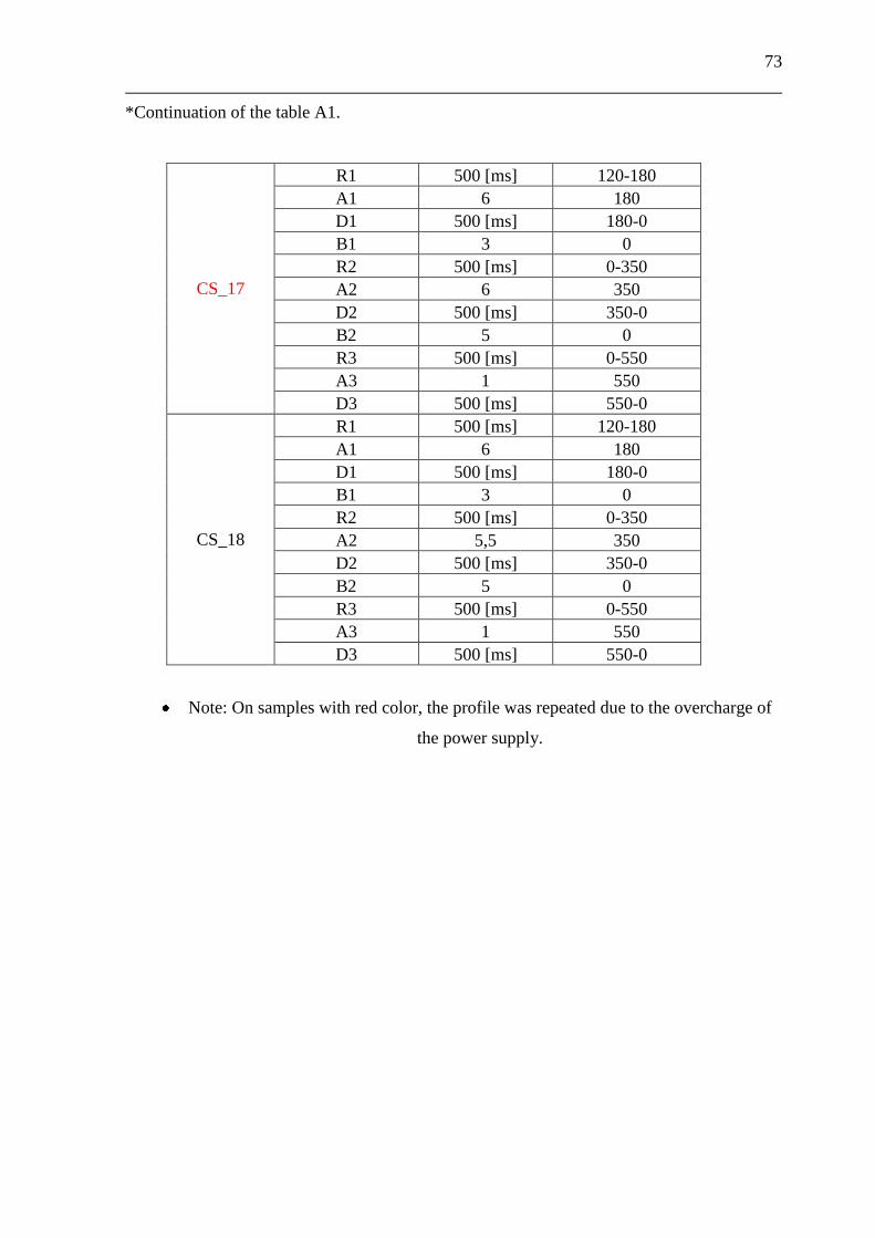
73
*Continuation of the table A1.
CS_17
R1 500 [ms] 120-180
A1 6 180
D1 500 [ms] 180-0
B1 3 0
R2 500 [ms] 0-350
A2 6 350
D2 500 [ms] 350-0
B2 5 0
R3 500 [ms] 0-550
A3 1 550
D3 500 [ms] 550-0
CS_18
R1 500 [ms] 120-180
A1 6 180
D1 500 [ms] 180-0
B1 3 0
R2 500 [ms] 0-350
A2 5,5 350
D2 500 [ms] 350-0
B2 5 0
R3 500 [ms] 0-550
A3 1 550
D3 500 [ms] 550-0
Note: On samples with red color, the profile was repeated due to the overcharge of
the power supply.