Datasheet 7-Mar-2022
CFR0011-120-00
Revision 2.6
1 of 301 © 2022 Renesas Electronics Corporation
SLG47004
GreenPAK Programmable Mixed-Signal Matrix with In-System Programmability and Advanced Analog Features
Preliminary
Key Features
Applications
General Description
The SLG47004 provides a small, low power component for commonly used analog signal processing and mixed-signalfunctions. Individual, tunable, analog components used in conjunction with configurable logic provide a way to solve a widevariety of tasks with minimal costs. The user creates their circuit design by programming the multiple time Non-VolatileMemory (NVM) to configure the interconnect logic, the analog and digital macrocell, and the IO Pins of the SLG47004.
Two Programmable Bandwidth Op Amps 3-Op Amp Instrumentation Amplifier Function
(including Additional Internal Op Amp) Rail to Rail Input Low Quiescent Current Low Offset Voltage Analog Comparator Mode Optional Vref Voltage Connection for Input Pins
Two 1024 Position Digital Rheostats User Defined Auto-Trim Option Manual Control Option I2C Control Option Potentiometer Mode
Two Single-Pole/Single-Throw Analog Switches Voltage or Current Source/Sink Mode
One Low Offset Chopper Comparator Two Low Power General Purpose ACMPs
ACMP Sampling Mode Hysteresis with Independently-Selectable Thresholds
Three Voltage References Two ACMP Vref Output Buffers One High Drive Buffer
Thirteen Combination Function Macrocells Three Selectable DFF/LATCH or 2-bit LUTs One Selectable Programmable Pattern Generator or
2-bit LUT Seven Selectable DFF/LATCH or 3-bit LUTs One Selectable Pipe Delay or Ripple Counter or
3-bit LUT One Selectable DFF/LATCH or 4-bit LUT
Seven Multi-Function Macrocells Six Selectable DFF/LATCH or 3-bit LUTs + 8-bit
Delay/Counters One Selectable DFF/LATCH or 4-bit LUT + 16-bit
Delay/Counter Serial Communications
I2C Protocol Interface 2-kbit (256 x 8) I2C-Compatible (2-Wire) Serial EEPROM
Emulation with Software Write Protection Programmable Delay with Edge Detector Output Deglitch Filter or Edge Detector Three Oscillators
2.048 kHz Oscillator 2.048 MHz Oscillator 25 MHz Oscillator
Analog Temperature Sensor Power-On Reset In-System Programmability Multiple Time Programmable Memory Wide Range Power Supply
2.5 V (±4 %) to 5 V (±10 %) VDD Operating Temperature Range: -40 °C to +85 °C RoHS Compliant/Halogen-Free Package Available
24-pin STQFN: 3 mm x 3 mm x 0.55 mm, 0.4 mm pitch
Adjust Precision Threshold Sensor Offset Trimming/Calibration Tunable Analog Filters Operational Amplifier Adjustable Gain and Offset Adjustable Voltage-to-Current Conversions Personal Computers and Servers PC Peripherals Consumer Electronics Data Communications Equipment Handheld and Portable Electronics Smartphones and Fitness Bands Notebook and Tablet PCs

Datasheet 7-Mar-2022
CFR0011-120-00
Revision 2.6
2 of 301 © 2022 Renesas Electronics Corporation
SLG47004
GreenPAK Programmable Mixed-Signal Matrix with In-System Programmability and Advanced Analog Features
Preliminary
Contents
General Description .................................................................................................................................................................1
Key Features ............................................................................................................................................................................1
Applications..............................................................................................................................................................................1
1 Block Diagram ....................................................................................................................................................................12
2 Pinout ..................................................................................................................................................................................13
2.1 Pin Configuration - STQFN-24L ...........................................................................................................................133 Characteristics ...................................................................................................................................................................16
3.1 Absolute Maximum Ratings .................................................................................................................................163.2 Electrostatic Discharge Ratings ...........................................................................................................................163.3 Recommended Operating Conditions ..................................................................................................................163.4 Electrical Characteristics ......................................................................................................................................173.5 I2C Pins Characteristics .......................................................................................................................................223.6 Macrocells Current Consumption .........................................................................................................................253.7 Timing Characteristics .........................................................................................................................................263.8 Oscillator Characteristics .....................................................................................................................................273.9 ACMP Characteristics ..........................................................................................................................................283.10 Internal Vref Characteristics ...............................................................................................................................293.11 Output Buffers Characteristics ...........................................................................................................................293.12 Analog Temperature Sensor Characteristics .....................................................................................................313.13 Programmable Operational Amplifier Characteristics ........................................................................................323.14 100K Digital Rheostat Characteristics ...............................................................................................................363.15 Analog Switches Characteristics .......................................................................................................................37
4 User Programmability ........................................................................................................................................................39
5 IO Pins .................................................................................................................................................................................40
5.1 GPIO Pins ............................................................................................................................................................405.2 GPI Pins ...............................................................................................................................................................405.3 Pull-Up/Down Resistors .......................................................................................................................................405.4 Fast Pull-Up/Down during Power-Up ...................................................................................................................405.5 I2C Mode IO Structure .........................................................................................................................................415.6 Matrix OE IO Structure .........................................................................................................................................425.7 GPI Structure .......................................................................................................................................................435.8 IO Pins Typical Performance ...............................................................................................................................44
6 Connection Matrix ..............................................................................................................................................................47
6.1 Matrix Input Table ................................................................................................................................................486.2 Matrix Output Table .............................................................................................................................................496.3 Connection Matrix Virtual Inputs ..........................................................................................................................526.4 Connection Matrix Virtual Outputs .......................................................................................................................53
7 Combination Function Macrocells ....................................................................................................................................54
7.1 2-Bit LUT or D Flip-Flop Macrocells .....................................................................................................................547.2 2-bit LUT or Programmable Pattern Generator ....................................................................................................577.3 3-Bit LUT or D Flip-Flop with Set/Reset Macrocells .............................................................................................597.4 4-Bit LUT or D Flip-Flop with Set/Reset Macrocell ...............................................................................................677.5 3-Bit LUT or Pipe Delay/Ripple Counter Macrocell ..............................................................................................69
8 Multi-Function Macrocells .................................................................................................................................................73
8.1 3-Bit LUT or DFF/Latch with 8-Bit Counter/Delay Macrocells ..............................................................................738.2 4-Bit LUT or DFF/Latch with 16-Bit Counter/Delay Macrocell ..............................................................................828.3 CNT/DLY/FSM Timing Diagrams .........................................................................................................................858.4 Wake and Sleep Controller ..................................................................................................................................94
9 Analog Comparators ..........................................................................................................................................................98
9.1 Analog Comparators Overview ............................................................................................................................989.2 Chopper Analog Comparator .............................................................................................................................1009.3 ACMP Sampling Mode .......................................................................................................................................1029.4 ACMP Typical Performance ...............................................................................................................................103
10 Programmable Operational Amplifiers .........................................................................................................................106
10.1 General Description .........................................................................................................................................106
Datasheet 7-Mar-2022
CFR0011-120-00
Revision 2.6
3 of 301 © 2022 Renesas Electronics Corporation
SLG47004
GreenPAK Programmable Mixed-Signal Matrix with In-System Programmability and Advanced Analog Features
Preliminary
10.2 Modes of Operation ..........................................................................................................................................10810.3 Op Amps Typical Performance ........................................................................................................................112
11 Analog Switch Macrocell ...............................................................................................................................................158
11.1 Analog Switch General Description ..................................................................................................................15811.2 Half Bridge Mode .............................................................................................................................................16011.3 Analog Switches Typical Performance .............................................................................................................161
12 Digital Rheostats and Programmable Trim Block .......................................................................................................163
12.1 Potentiometer Mode .........................................................................................................................................16612.2 Calculating Actual Resistance ..........................................................................................................................16612.3 Digital Rheostat Value Self-programming into the NVM ..................................................................................16712.4 Trimming process Using Programmable Trim Block ........................................................................................17012.5 Using Chopper ACMP ......................................................................................................................................176
13 Programmable Delay/Edge Detector ............................................................................................................................182
13.1 Programmable Delay Timing Diagram - Edge Detector Output .......................................................................18214 Additional Logic Function. Deglitch Filter ...................................................................................................................183
15 Voltage Reference ..........................................................................................................................................................184
15.1 Voltage Reference Overview ...........................................................................................................................18415.2 Vref Selection Table ........................................................................................................................................18415.3 Vref Block Diagram ..........................................................................................................................................18615.4 Voltage Reference Typical Performance .........................................................................................................19015.5 HD Buffer Typical Performance .......................................................................................................................193
16 Clocking ..........................................................................................................................................................................197
16.1 OSC General Description .................................................................................................................................19716.2 Oscillator0 (2.048 kHz) .....................................................................................................................................19816.3 Oscillator1 (2.048 MHz) ...................................................................................................................................19916.4 Oscillator2 (25 MHz) ........................................................................................................................................20016.5 CNT/DLY Clock Scheme ..................................................................................................................................20016.6 External Clocking .............................................................................................................................................20116.7 Oscillators Power-On Delay .............................................................................................................................20216.8 Oscillators Accuracy .........................................................................................................................................20416.9 Oscillators Settling time ....................................................................................................................................20616.10 Oscillators Current Consumption ..................................................................................................................208
17 Power-On Reset ..............................................................................................................................................................212
17.1 General Operation ............................................................................................................................................21217.2 POR Sequence ................................................................................................................................................21317.3 Macrocells Output States During POR Sequence ...........................................................................................213
18 I2C Serial Communications Macrocell ..........................................................................................................................216
18.1 I2C Serial Communications Macrocell Overview ..............................................................................................21618.2 I2C Serial Communications Device Addressing ...............................................................................................21618.3 I2C Serial General Timing ................................................................................................................................21718.4 I2C Serial Communications Commands ...........................................................................................................21718.5 Chip Configuration Data Protection ..................................................................................................................22018.6 I2C Serial Command Register Map ..................................................................................................................22118.7 I2C Additional Options ......................................................................................................................................224
19 Non-Volatile Memory ......................................................................................................................................................226
19.1 Serial NVM Write Operations ...........................................................................................................................22619.2 Serial NVM Read Operations ...........................................................................................................................22819.3 Serial NVM Erase Operations ..........................................................................................................................22819.4 Acknowledge Polling ........................................................................................................................................22919.5 Low power standby mode ................................................................................................................................22919.6 Emulated EEPROM Write Protection ...............................................................................................................229
20 Analog Temperature Sensor .........................................................................................................................................231
21 Register Definitions .......................................................................................................................................................234
21.1 Register Map ....................................................................................................................................................23422 Package Top Marking System Definition .....................................................................................................................293
22.1 STQFN-24L 3 mm x 3 mm x 0.55 mm, 0.4P FCD Package ............................................................................29323 Package Information ......................................................................................................................................................294

Datasheet 7-Mar-2022
CFR0011-120-00
Revision 2.6
4 of 301 © 2022 Renesas Electronics Corporation
SLG47004
GreenPAK Programmable Mixed-Signal Matrix with In-System Programmability and Advanced Analog Features
Preliminary
23.1 Package outlines FOR STQFN 24L 3 mm x 3 mm x 0.55 mm 0.4P Green Package ......................................29423.2 STQFN Handling ..............................................................................................................................................29423.3 Soldering Information .......................................................................................................................................294
24 Ordering Information .....................................................................................................................................................295
24.1 Tape and Reel Specifications ..........................................................................................................................29524.2 Carrier Tape Drawing and Dimensions ............................................................................................................295
25 Layout Guidelines ..........................................................................................................................................................296
25.1 STQFN 24L 3 mm x 3 mm x 0.55 mm 0.4P Green Package ...........................................................................296Glossary................................................................................................................................................................................297
Revision History...................................................................................................................................................................300

Datasheet 7-Mar-2022
CFR0011-120-00
Revision 2.6
5 of 301 © 2022 Renesas Electronics Corporation
SLG47004
GreenPAK Programmable Mixed-Signal Matrix with In-System Programmability and Advanced Analog Features
Preliminary
Figures
Figure 1: Block Diagram...........................................................................................................................................................12Figure 2: Steps to Create a Custom GreenPAK Device...........................................................................................................39Figure 3: IO with I2C Mode IO Structure Diagram....................................................................................................................41Figure 4: Matrix OE IO Structure Diagram ...............................................................................................................................42Figure 5: IO0 GPI Structure Diagram.......................................................................................................................................43Figure 6: Typical High Level Output Current vs. High Level Output Voltage at T = 25 °C .......................................................44Figure 7: Typical Low Level Output Current vs. Low Level Output Voltage, 1x Drive at T = 25 °C, Full Range ......................44Figure 8: Typical Low Level Output Current vs. Low Level Output Voltage, 1x Drive at T = 25 °C .........................................45Figure 9: Typical Low Level Output Current vs. Low Level Output Voltage, 2x Drive at T = 25 °C, Full Range ......................45Figure 10: Typical Low Level Output Current vs. Low Level Output Voltage, 2x Drive at T = 25 °C .......................................46Figure 11: Connection Matrix ...................................................................................................................................................47Figure 12: Connection Matrix Example ....................................................................................................................................47Figure 13: 2-bit LUT0 or DFF0 .................................................................................................................................................54Figure 14: 2-bit LUT1 or DFF1 .................................................................................................................................................55Figure 15: 2-bit LUT2 or DFF2 .................................................................................................................................................55Figure 16: DFF Polarity Operations..........................................................................................................................................57Figure 17: 2-bit LUT3 or PGen.................................................................................................................................................58Figure 18: PGen Timing Diagram.............................................................................................................................................58Figure 19: 3-bit LUT0 or DFF3 .................................................................................................................................................60Figure 20: 3-bit LUT1 or DFF4 .................................................................................................................................................61Figure 21: 3-bit LUT2 or DFF5 .................................................................................................................................................61Figure 22: 3-bit LUT3 or DFF6 .................................................................................................................................................62Figure 23: 3-bit LUT4 or DFF7 .................................................................................................................................................62Figure 25: 3-bit LUT6 or DFF9 .................................................................................................................................................63Figure 24: 3-bit LUT5 or DFF8 .................................................................................................................................................63Figure 26: DFF Polarity Operations with nReset......................................................................................................................66Figure 27: DFF Polarity Operations with nSet..........................................................................................................................67Figure 28: 4-bit LUT0 or DFF10 ...............................................................................................................................................68Figure 29: 3-bit LUT13/Pipe Delay/Ripple Counter ..................................................................................................................70Figure 30: Example: Ripple Counter Functionality ...................................................................................................................71Figure 31: Possible Connections Inside Multi-Function Macrocell ...........................................................................................73Figure 32: 8-bit Multi-Function Macrocells Block Diagram (3-bit LUT7/DFF11, CNT/DLY1) ...................................................74Figure 33: 8-bit Multi-Function Macrocells Block Diagram (3-bit LUT8/DFF12, CNT/DLY2) ...................................................75Figure 34: 8-bit Multi-Function Macrocells Block Diagram (3-bit LUT9/DFF13, CNT/DLY3) ...................................................76Figure 35: 8-bit Multi-Function Macrocells Block Diagram (3-bit LUT10/DFF14, CNT/DLY4) .................................................77Figure 36: 8-bit Multi-Function Macrocells Block Diagram (3-bit LUT11/DFF15, CNT/DLY5) .................................................78Figure 37: 8-bit Multi-Function Macrocells Block Diagram (3-bit LUT12/DFF16, CNT/DLY6) .................................................79Figure 38: 4-bit LUT1 or CNT/DLY0.........................................................................................................................................83Figure 39: Delay Mode Timing Diagram, Edge Select: Both, Counter Data: 3 ........................................................................85Figure 40: Delay Mode Timing Diagram for Different Edge Select Modes...............................................................................86Figure 41: Counter Mode Timing Diagram without Two DFFs Synced Up ..............................................................................86Figure 42: Counter Mode Timing Diagram with Two DFFs Synced Up ...................................................................................87Figure 43: One-Shot Function Timing Diagram........................................................................................................................88Figure 44: Frequency Detection Mode Timing Diagram...........................................................................................................89Figure 45: Edge Detection Mode Timing Diagram ...................................................................................................................90Figure 46: Delayed Edge Detection Mode Timing Diagram.....................................................................................................91Figure 47: CNT/FSM Timing Diagram (Reset Rising Edge Mode, Oscillator is Forced On, UP = 0) for Counter Data = 3 .....91Figure 48: CNT/FSM Timing Diagram (Set Rising Edge Mode, Oscillator is Forced On, UP = 0) for Counter Data = 3 .........92Figure 49: CNT/FSM Timing Diagram (Reset Rising Edge Mode, Oscillator is Forced On, UP = 1) for Counter Data = 3 .....92Figure 50: CNT/FSM Timing Diagram (Set Rising Edge Mode, Oscillator is Forced On, UP = 1) for Counter Data = 3 .........93Figure 51: Counter Value, Counter Data = 3............................................................................................................................93Figure 52: Wake and Sleep Controller .....................................................................................................................................94Figure 53: Wake and Sleep Timing Diagram, Normal Wake Mode, Counter Reset is Used ...................................................95Figure 54: Wake and Sleep Timing Diagram, Short Wake Mode, Counter Reset is Used ......................................................95Figure 55: Wake and Sleep Timing Diagram, Normal Wake Mode, Counter Set is Used .......................................................96

Datasheet 7-Mar-2022
CFR0011-120-00
Revision 2.6
6 of 301 © 2022 Renesas Electronics Corporation
SLG47004
GreenPAK Programmable Mixed-Signal Matrix with In-System Programmability and Advanced Analog Features
Preliminary
Figure 56: Wake and Sleep Timing Diagram, Short Wake Mode, Counter Set is Used ..........................................................96Figure 57: ACMP0L Block Diagram .........................................................................................................................................99Figure 58: ACMP1L Block Diagram .......................................................................................................................................100Figure 59: Chopper ACMP Block Diagram.............................................................................................................................102Figure 60: Propagation Delay vs. Vref for ACMPx at T = 25 °C, VDD = 2.4 V to 5.5 V, Hysteresis = 0 .................................103Figure 61: ACMPx Power-On Delay vs. VDD at BG - Forced.................................................................................................103Figure 62: ACMPx Input Offset Voltage vs. Vref at T = -40 °C to 85 °C, VDD = 2.4 V to 5.5 V, Gain = 1 ..............................104Figure 63: Chopper ACMP Input Offset Voltage vs. Vref at T = -40 °C to 85 °C, VDD = 2.4 V to 5.5 V, Gain = 1 .................104Figure 64: ACMPx Current Consumption vs. VDD................................................................................................................................................105Figure 65: Chopper ACMP Current Consumption vs. VDD (with 2.048 kHz Clock)................................................................105Figure 66: Programmable Operational Amplifier OA0, OA1 Internal Circuit ..........................................................................106Figure 67: Internal Operational Amplifier Circuit ....................................................................................................................107Figure 68: Example of Input Offset Voltage Compensation ...................................................................................................108Figure 69: Instrumentation Amplifier Structure.......................................................................................................................109Figure 70: Instrumentation Operational Amplifier Configuration for Users Trim.....................................................................110Figure 71: Typical Implementation of Voltage Regulator (A) and Current Sources (B, C) .....................................................111Figure 72: Constant Current Sink...........................................................................................................................................112Figure 73: Op Ampx Input Offset Voltage vs. TA at Input CM Voltage = VDD/2, BW = 128 kHz............................................. 112Figure 74: Op Ampx Input Offset Voltage vs. TA at Input CM Voltage = VDD/2, BW = 512 kHz............................................. 113Figure 75: Op Ampx Input Offset Voltage vs. TA at Input CM Voltage = VDD/2, BW = 2 MHz ............................................... 113Figure 76: Op Ampx Input Offset Voltage vs. TA at Input CM Voltage = VDD/2, BW = 8 MHz ............................................... 114Figure 77: Internal Op Amp Input Offset Voltage vs. TA at Input CM Voltage = VDD/2, BW = 128 kHz ................................. 114Figure 78: Internal Op Amp at Input CM Voltage = VDD/2, BW = 512 kHz............................................................................. 115Figure 79: Internal Op Amp at Input CM Voltage = VDD/2, BW = 2 MHz ............................................................................... 115Figure 80: Internal Op Amp Input Offset Voltage vs. TA at Input CM Voltage = VDD/2, BW = 8 MHz .................................... 116Figure 81: OpAmp0, 1 Input Offset Voltage vs. Input CM Voltage at T = 25 °C, VDDA = 2.4 V ............................................116Figure 82: OpAmp0, 1 Input Offset Voltage vs. Input CM Voltage at T = 25 °C, VDDA = 5.5 V ............................................117Figure 83: Internal OpAmp Input Offset Voltage vs. Input CM Voltage at T = 25 °C, VDDA = 2.4 V .....................................117Figure 84: Internal OpAmp Input Offset Voltage vs. Input CM Voltage at T = 25 °C, VDDA = 5.5 V .....................................118Figure 85: Quiescent Current vs. Power Supply Voltage for BW = 128 kHz.......................................................................... 118Figure 86: Quiescent Current vs. Power Supply Voltage for BW = 512 kHz.......................................................................... 119Figure 87: Quiescent Current vs. Power Supply Voltage for BW = 2 MHz ............................................................................ 119Figure 88: Quiescent Current vs. Power Supply Voltage or BW = 8 MHz .............................................................................120Figure 89: OA0 Open Loop Gain and Phase vs. Frequency for BW = 128 kHz ....................................................................120Figure 90: OA0 Open Loop Gain and Phase vs. Frequency for BW = 512 kHz ....................................................................121Figure 91: OA0 Open Loop Gain and Phase vs. Frequency for BW = 2 MHz .......................................................................121Figure 92: OA0 Open Loop Gain and Phase vs. Frequency for BW = 8 MHz .......................................................................122Figure 93: OA1 Open Loop Gain and Phase vs. Frequency for BW = 128 kHz ....................................................................122Figure 94: OA1 Open Loop Gain and Phase vs. Frequency for BW = 512 kHz ....................................................................123Figure 95: OA1 Open Loop Gain and Phase vs. Frequency for BW = 2 MHz .......................................................................123Figure 96: OA1 Open Loop Gain and Phase vs. Frequency for BW = 8 MHz .......................................................................124Figure 97: PSRR vs. Frequency VDD = 2.4 V to 5.5 V ..........................................................................................................124Figure 98: 0.1 Hz to 10 Hz Noise, BW = 128 kHz ..................................................................................................................125Figure 99: 0.1 Hz to 10 Hz Noise, BW = 512 kHz ..................................................................................................................125Figure 100: 0.1 Hz to 10 Hz Noise, BW = 2 MHz...................................................................................................................126Figure 101: 0.1 Hz to 10 Hz Noise, BW = 2 MHz...................................................................................................................126Figure 102: Channel Separation vs. Frequency.....................................................................................................................127Figure 103: Op Ampx Noise Voltage Density vs. Frequency..................................................................................................127Figure 104: Slew Rate vs. Ambient Temperature G = 1 V/V; RL = 50 kΩ for BW = 128 kHz ................................................128Figure 105: Slew Rate vs. Ambient Temperature G = 1 V/V; RL = 50 kΩ for BW = 512 kHz ................................................128Figure 106: Slew Rate vs. Ambient Temperature G = 1 V/V; RL = 50 kΩ for BW = 2 MHz ...................................................129Figure 107: Slew Rate vs. Ambient Temperature G = 1 V/V; RL = 50 kΩ for BW = 8 MHz....................................................129Figure 108: Small Signal Inverting Step Response G = -1 V/V, RL = 50 kΩ, CL = 60 pF, BW = 128 kHz..............................130Figure 109: Small Signal Inverting Step Response G = -1 V/V, RL = 50 kΩ, CL = 60 pF, BW = 512 kHz..............................130Figure 110: Small Signal Inverting Step Response G = -1 V/V, RL = 50 kΩ, CL = 60 pF, BW = 2 MHz ................................131Figure 111: Small Signal Inverting Step Response G = -1 V/V, RL = 50 kΩ, CL = 60 pF, BW = 8 MHz ................................131Figure 112: Small Signal Non-Inverting Step Response G = -1 V/V, RL = 50 kΩ, CL = 60 pF, BW = 128 kHz......................132

Datasheet 7-Mar-2022
CFR0011-120-00
Revision 2.6
7 of 301 © 2022 Renesas Electronics Corporation
SLG47004
GreenPAK Programmable Mixed-Signal Matrix with In-System Programmability and Advanced Analog Features
Preliminary
Figure 113: Small Signal Non-Inverting Step Response G = -1 V/V, RL = 50 kΩ, CL = 60 pF, BW = 512 kHz......................132Figure 114: Small Signal Non-Inverting Step Response G = -1 V/V, RL = 50 kΩ, CL = 60 pF, BW = 2 MHz.........................133Figure 115: Small Signal Non-Inverting Step Response G = -1 V/V, RL = 50 kΩ, CL = 60 pF, BW = 8 MHz.........................133Figure 116: Large Signal Inverting Step Response G = -1 V/V, RL = 50 kΩ, CL = 80 pF, BW = 128 kHz .............................134Figure 117: Large Signal Inverting Step Response G = -1 V/V, RL = 50 kΩ, CL = 80 pF, BW = 512kHz ..............................134Figure 118: Large Signal Inverting Step Response G = -1 V/V, RL = 50 kΩ, CL = 80 pF, BW = 2 MHz ................................135Figure 119: Large Signal Inverting Step Response G = -1 V/V, RL = 50 kΩ, CL = 80 pF, BW = 8 MHz ................................135Figure 120: Large Signal Non-Inverting Step Response G = -1 V/V, RL = 50 kΩ, CL = 60 pF, BW = 128 kHz......................136Figure 121: Large Signal Non-Inverting Step Response G = -1 V/V, RL = 50 kΩ, CL = 60 pF, BW = 512 kHz......................136Figure 122: Large Signal Non-Inverting Step Response G = -1 V/V, RL = 50 kΩ, CL = 60 pF, BW = 2 MHz ........................137Figure 123: Large Signal Non-Inverting Step Response G = -1 V/V, RL = 50 kΩ, CL = 60 pF, BW = 8 MHz ........................137Figure 124: Inverting Overload Recovery G = -1 V/V, RL = 50 kΩ, CL = 60 pF, BW = 128 kHz ............................................138Figure 125: Inverting Overload Recovery G = -1 V/V, RL = 50 kΩ, CL = 60 pF, BW = 512 kHz ............................................138Figure 126: Inverting Overload Recovery G = -1 V/V, RL = 50 kΩ, CL = 60 pF, BW = 2 MHz ...............................................139Figure 127: Inverting Overload Recovery G = -1 V/V, RL = 50 kΩ, CL = 60 pF, BW = 8 MHz ...............................................139Figure 128: Non-Inverting Overload Recovery G = -1 V/V, RL = 50 kΩ, CL = 60 pF, BW = 128 kHz.....................................140Figure 129: Non-Inverting Overload Recovery G = -1 V/V, RL = 50 kΩ, CL = 60 pF, BW = 512 kHz.....................................140Figure 130: Non-Inverting Overload Recovery G = -1 V/V, RL = 50 kΩ, CL = 60 pF, BW = 2 MHz .......................................141Figure 131: Non-Inverting Overload Recovery G = -1 V/V, RL = 50 kΩ, CL = 60 pF, BW = 8 MHz .......................................141Figure 132: Small Signal Overshoot vs. Capacitive Load VDD = 3.3 V, G = 1 V/V, BW = 128 kHz.......................................142Figure 133: Small Signal Overshoot vs. Capacitive Load VDD = 3.3 V, G = 1 V/V, BW = 512 kHz.......................................142Figure 134: Small Signal Overshoot vs. Capacitive Load VDD = 3.3 V, G = 1 V/V, BW = 2 MHz..........................................143Figure 135: Small Signal Overshoot vs. Capacitive Load VDD = 3.3 V, G = 1 V/V, BW = 8 MHz..........................................143Figure 136: Output Voltage Low (VOUT - GND) vs. Temperature at BW = 128 kHz, RLOAD = 600 Ω....................................144Figure 137: Output Voltage Low (VOUT - GND) vs. Temperature at BW = 128 kHz, RLOAD = 50 kΩ ....................................144Figure 138: Output Voltage High (VDDA- VOUT) vs. Temperature at BW = 128 kHz, RLOAD = 600 Ω....................................145Figure 139: Output Voltage High (VDDA- VOUT) vs. Temperature at BW = 128 kHz, RLOAD = 50 kΩ....................................145Figure 140: Output Voltage Low (VOUT - GND) vs. Temperature at BW = 512 kHz, RLOAD = 50 kΩ ....................................146Figure 141: Output Voltage Low (VOUT - GND) vs. Temperature at BW = 512 kHz, RLOAD = 50 kΩ ....................................146Figure 142: Output Voltage High (VDDA- VOUT) vs. Temperature at BW = 512 kHz, RLOAD = 600 Ω....................................147Figure 143: Output Voltage High (VDDA- VOUT) vs. Temperature at BW = 512kHz, RLOAD = 50 kΩ.....................................147Figure 144: Output Voltage Low (VOUT - GND) vs. Temperature at BW = 2 MHz, RLOAD = 600 Ω.......................................148Figure 145: Output Voltage Low (VOUT - GND) vs. Temperature at BW = 2 MHz, RLOAD = 50 kΩ.......................................148Figure 146: Output Voltage High (VDDA- VOUT) vs. Temperature at BW = 2 MHz, RLOAD = 600 Ω ......................................149Figure 147: Output Voltage High (VDDA- VOUT) vs. Temperature at BW = 2 MHz, RLOAD = 50 kΩ.......................................149Figure 148: Output Voltage Low (VOUT - GND) vs. Temperature at BW = 8MHz, RLOAD = 600 Ω........................................150Figure 149: Output Voltage Low (VOUT - GND) vs. Temperature at BW = 8 MHz, RLOAD = 50 kΩ.......................................150Figure 150: Output Voltage High (VDDA- VOUT) vs. Temperature at BW = 8 MHz, RLOAD = 600 Ω ......................................151Figure 151: Output Voltage High (VDDA- VOUT) vs. Temperature at BW = 8 MHz, RLOAD = 50 kΩ.......................................151Figure 152: Overload Recovery Time vs. Power Supply Voltage RL= 50 kΩ; G = 1 V/V, Rising...........................................152Figure 153: Overload Recovery Time vs. Power Supply Voltage RL= 50 kΩ; G = 1 V/V, Falling ..........................................152Figure 154: Output Response to Power Down Signal G = 1 V/V; RL = 50 kΩ; CL = 20 pF; VIN = VS/2, BW = 128 kHz ......153Figure 155: Output Response to Power Down Signal G = 1 V/V; RL = 50 kΩ; CL = 20 pF; VIN = VS/2, BW = 512 kHz ......153Figure 156: Output Response to Power Down Signal G = 1 V/V; RL = 50 kΩ; CL = 20 pF; VIN = VS/2, BW = 2 MHz .........154Figure 157: Output Response to Power Down Signal G = 1 V/V; RL = 50 kΩ; CL = 20 pF; VIN = VS/2, BW = 8 MHz .........154Figure 158: Opampx Turn-On/Off Time vs. VDD at VIN = VDD/2, BW = 128 kHz ................................................................155Figure 159: Opampx Turn-On/Off Time vs. VDD at VIN = VDD/2, BW = 512 kHz ................................................................155Figure 160: Opampx Turn-On/Off Time vs. VDD at VIN = VDD/2, BW = 2 MHz ...................................................................156Figure 161: Opampx Turn-On/Off Time vs. VDD at VIN = VDD/2, BW = 8MHz ....................................................................156Figure 162: Opamps Quiescent Current Consumption vs. VDD ......................................................................................................................157Figure 163: Analog Switch 0 Control Circuit...........................................................................................................................158Figure 164: Analog Switch 1 Control Circuit...........................................................................................................................159Figure 165: Structure of Half Bridge.......................................................................................................................................160Figure 166: Typical RON vs. Input Voltage (Vi) for Vi = 0 to VDDA, ILOAD = 1 mA, VDDA = 2.4 V................................................161Figure 167: Typical RON vs. Input Voltage (Vi) for Vi = 0 to VDDA, ILOAD = 1 mA, VDDA = 5.5 V................................................161Figure 168: Turn-On Time vs. VDD at RLOAD = 100 Ω to GND, VIN = VDD/2 .......................................................................................................162Figure 169: Turn-Off Time vs. VDD at RLOAD = 100 Ω to GND, VIN = VDD/2 .......................................................................................................162

Datasheet 7-Mar-2022
CFR0011-120-00
Revision 2.6
8 of 301 © 2022 Renesas Electronics Corporation
SLG47004
GreenPAK Programmable Mixed-Signal Matrix with In-System Programmability and Advanced Analog Features
Preliminary
Figure 170: Programmable Trim Blocks and Digital Rheostat’s Internal Circuit.....................................................................165Figure 171: Rheostats in Potentiometer Mode......................................................................................................................166Figure 172: Rheostat Tolerance Registers............................................................................................................................167Figure 173: Flowchart of "Program" and "Reload" Signals ....................................................................................................168Figure 174: Example of Latching and Processing "Program" and "Reload" Signals..............................................................169Figure 175: Example of Auto-Trim Process for a Single Rheostat.........................................................................................171Figure 176: Example of Auto-Trim Process with External Clock Signal.................................................................................172Figure 177: Example of Auto-Trim Process for Two Rheostats .............................................................................................173Figure 178: Example of Auto-Trim Process via I2C................................................................................................................174Figure 179: Example of Hardware Configuration ...................................................................................................................175Figure 180: Example of User Specific Trimming Process under I2C Master Control .............................................................176Figure 181: DNL vs. Digital Code, Rheostat Mode (VAB = 1 V) at T = 25 °C.........................................................................177Figure 182: INL vs. Digital Code, Rheostat Mode (VAB = 1 V) at T = 25 °C ..........................................................................177Figure 183: DNL vs. Digital Code, Potentiometer Mode (VAB = 1 V) at T = 25 °C.................................................................178Figure 184: INL vs. Digital Code, Potentiometer Mode (VAB = 1 V) at T = 25 °C ..................................................................178Figure 185: (ΔRAB/RAB)/ΔTA Rheostat Mode Tempco...........................................................................................................179Figure 186: RHx Zero Scale Error vs. Temperature (VIN = 1 V) ............................................................................................179Figure 187: Transition Glitch in Worst Case (Code = 511 to Code = 512).............................................................................180Figure 188: Gain vs. Frequency (Code = 512) at T = 25 °C, VDDA = 5 V...............................................................................180Figure 189: RHx Settling Time vs. VDD at ILOAD = 1 mA, T = 25 °C .........................................................................................181Figure 190: Programmable Delay ..........................................................................................................................................182Figure 191: Edge Detector Output .........................................................................................................................................182Figure 192: Deglitch Filter or Edge Detector ..........................................................................................................................183Figure 193: Generalized Vref Structure..................................................................................................................................186Figure 194: ACMP0L, ACMP1L Voltage Reference Block Diagram ......................................................................................187Figure 195: HD Buffer and Chopper ACMP Reference Block Diagram .................................................................................188Figure 196: Operational Amplifiers Voltage Reference Block Diagram..................................................................................189Figure 197: Typical Load Regulation, Vref = 320 mV, T = -40 °C to +85 °C, Buffer - Enable................................................190Figure 198: Typical Load Regulation, Vref = 640 mV, T = -40 °C to +85 °C, Buffer - Enable................................................190Figure 199: Typical Load Regulation, Vref = 1280 mV, T = -40 °C to +85 °C, Buffer - Enable..............................................191Figure 200: Typical Load Regulation, Vref = 2048 mV, T = -40 °C to +85 °C, Buffer - Enable..............................................191Figure 201: Typical Input Offset Voltage vs. Vref at VDD = 2.4 V to 5.5 V, T = 25 °C, Buffer Disabled .................................192Figure 202: Op Ampx Vref Divider Acuuracy at VDD = 3.3 V .................................................................................................192Figure 203: HD Buffer Typical Load Regulation, Vref = 320 mV, T = -40 °C to +85 °C.........................................................193Figure 204: HD Buffer Typical Load Regulation, Vref = 640 mV, T = -40 °C to +85 °C.........................................................193Figure 205: HD Buffer Typical Load Regulation, Vref = 1280 mV, T = -40 °C to +85 °C.......................................................194Figure 206: HD Buffer Typical Load Regulation, Vref = 2048 mV, T = -40 °C to +85 °C.......................................................194Figure 207: HD Buffer Typical Line Regulation, ILOAD = 5 mA...............................................................................................195Figure 208: HD Buffer Offset vs. VDD........................................................................................................................................................................195Figure 209: HD Buffer Output Short-Circuit Current vs. VDD............................................................................................................................196Figure 210: Oscillator0 Block Diagram...................................................................................................................................198Figure 211: Oscillator1 Block Diagram...................................................................................................................................199Figure 212: Oscillator2 Block Diagram...................................................................................................................................200Figure 213: Clock Scheme.....................................................................................................................................................201Figure 214: Oscillator Startup Diagram..................................................................................................................................202Figure 215: OSC0 Maximum Power-On Delay vs. VDD at T = 25 °C, OSC0 = 2.048 kHz ....................................................202Figure 216: OSC1 Oscillator Maximum Power-On Delay vs. VDD at T = 25 °C, OSC1 = 2.048 MHz....................................203Figure 217: OSC2 Maximum Power-On Delay vs. VDD at T = 25 °C, OSC2 = 25 MHz.........................................................203Figure 218: OSC0 Frequency vs. Temperature, OSC0 = 2.048 kHz .....................................................................................204Figure 219: OSC1 Frequency vs. Temperature, OSC1 = 2.048 MHz....................................................................................204Figure 220: OSC2 Frequency vs. Temperature, OSC2 = 25 MHz.........................................................................................205Figure 221: Oscillators Total Error vs. Temperature at VDD = 2.4 V to 5.5 V.........................................................................205Figure 222: Oscillator0 Settling Time, VDD = 3.3 V, T = 25 °C, OSC0 = 2 kHz......................................................................206Figure 223: Oscillator1 Settling Time, VDD = 3.3 V, T = 25 °C, OSC1 = 2 MHz ....................................................................206Figure 224: Oscillator2 Settling Time, VDD = 3.3 V, T = 25 °C, OSC2 = 25 MHz (Normal Start) ...........................................207Figure 225: Oscillator2 Settling Time, VDD = 3.3 V, T = 25 °C, OSC2 = 25 MHz (Start with Delay) ......................................207Figure 226: OSC1 Current Consumption vs. VDD (Pre-Divider = 1).......................................................................................208

Datasheet 7-Mar-2022
CFR0011-120-00
Revision 2.6
9 of 301 © 2022 Renesas Electronics Corporation
SLG47004
GreenPAK Programmable Mixed-Signal Matrix with In-System Programmability and Advanced Analog Features
Preliminary
Figure 227: OSC1 Current Consumption vs. VDD (Pre-Divider = 4).......................................................................................208Figure 228: OSC1 Current Consumption vs. VDD (Pre-Divider = 8).......................................................................................209Figure 229: OSC2 Current Consumption vs. VDD (Pre-Divider = 1).......................................................................................209Figure 230: OSC2 Current Consumption vs. VDD (Pre-Divider = 4).......................................................................................210Figure 231: OSC2 Current Consumption vs. VDD (Pre-Divider = 8).......................................................................................211Figure 232: POR Sequence ...................................................................................................................................................213Figure 233: Internal Macrocell States During POR Sequence...............................................................................................214Figure 234: Power-Down........................................................................................................................................................215Figure 235: Basic Command Structure ..................................................................................................................................216Figure 236: I2C General Timing Characteristics.....................................................................................................................217Figure 237: Byte Write Command, R/W = 0...........................................................................................................................217Figure 238: Sequential Write Command ................................................................................................................................218Figure 239: Current Address Read Command, R/W = 1........................................................................................................218Figure 240: Random Read Command ...................................................................................................................................219Figure 241: Sequential Read Command................................................................................................................................219Figure 242: Reset Command Timing .....................................................................................................................................220Figure 243: Example of I2C Byte Write Bit Masking...............................................................................................................225Figure 244: Page Write Command.........................................................................................................................................227Figure 245: I2C Block Addressing ..........................................................................................................................................228Figure 246: Analog Temperature Sensor Structure Diagram.................................................................................................232Figure 247: TS Output vs. Temperature, VDD = 3.3 V ...........................................................................................................233

Datasheet 7-Mar-2022
CFR0011-120-00
Revision 2.6
10 of 301 © 2022 Renesas Electronics Corporation
SLG47004
GreenPAK Programmable Mixed-Signal Matrix with In-System Programmability and Advanced Analog Features
Preliminary
Tables
Table 1: Functional Pin Description......................................................................................................................................... 13Table 2: Pin Type Definitions ................................................................................................................................................... 15Table 3: Absolute Maximum Ratings........................................................................................................................................ 16Table 4: Electrostatic Discharge Ratings ................................................................................................................................. 16Table 5: Recommended Operating Conditions ........................................................................................................................ 16Table 6: EC at T = -40 °C to +85 °C, VDD = 2.4 V to 5.5 V Unless Otherwise Noted ............................................................. 17Table 7: EC of the I2C Pins for DI at T = -40 °C to +85 °C, VDD = 2.4 V to 5.5 V Unless Otherwise Noted ........................... 22Table 8: EC of the I2C Pins for DILV at T = -40 °C to +85 °C, VDD = 2.4 V to 5.5 V Unless Otherwise Noted ....................... 23Table 9: I2C Pins Timing Characteristics for DI at T = -40 °C to +85 °C, VDD = 2.4 V to 5.5 V Unless Otherwise Noted....... 23Table 10: I2C Pins Timing Characteristics for DILV at T = -40 °C to +85 °C, VDD = 2.4 V to 5.5 V Unless Otherwise Noted 24Table 11: Typical Current Estimated for Each Macrocell at T = 25°C...................................................................................... 25Table 12: Typical Delay Estimated for Each Macrocell at T = 25 °C........................................................................................ 26Table 13: Programmable Delay Expected Typical Delays and Widths at T = 25 °C................................................................ 26Table 14: Typical Filter Rejection Pulse Width at T = 25 °C .................................................................................................... 27Table 15: Typical Counter/Delay Offset Measurements at T = 25 °C ...................................................................................... 27Table 16: Oscillators Frequency Limits, VDD = 2.4 V to 5.5 V.................................................................................................. 27Table 17: Oscillators Power-On Delay at T = 25 °C, OSC Power Setting: "Auto Power-On" .................................................. 28Table 18: ACMP Specifications at T = -40 °C to +85 °C, VDD = 2.4 V to 5.5 V Unless Otherwise Noted............................... 28Table 19: Internal Vref Characteristics at VDD = 2.4 V to 5.5 V .............................................................................................. 29Table 20: HD Buffer Electrical Characteristics at T = -40 °C to +85 °C, VDD = 2.4 V to 5.5 V Unless Otherwise Noted ........ 29Table 21: Vref Output Buffer at T = -40 °C to +85 °C, VDD = 2.4 V to 5.5 V Unless Otherwise Noted ................................... 29Table 22: TS Output vs Temperature (Output Range 1) .......................................................................................................... 31Table 23: TS Output vs Temperature (Output Range 2) .......................................................................................................... 31Table 24: EC of OA, VDDA = 2.4 V to 5.5 V, VCM = VDDA/2, VOUT ≈ VDDA/2, RL = 100 kΩ to VDDA/2, CL = 50 pF, T = 25 °C. 32Table 25: 100K Digital Rheostat EC at VA=VDD, VB=GND, T=-40°C to +85°C, VDD=2.4V to 5.5V Unless Otherwise Noted36Table 26: Analog Switch0/Voltage Regulator EС at T = -40 °C to +85 °C, VDD = 2.4 V to 5.5 V Unless Otherwise Noted.... 37Table 27: Analog Switch1/Current Sink EС at T = -40 °C to +85 °C, VDD = 2.4 V to 5.5 V Unless Otherwise Noted............. 38Table 28: Matrix Input Table..................................................................................................................................................... 48Table 29: Matrix Output Table.................................................................................................................................................. 49Table 30: Connection Matrix Virtual Inputs .............................................................................................................................. 53Table 31: 2-bit LUT0 Truth Table ............................................................................................................................................. 56Table 32: 2-bit LUT1 Truth Table ............................................................................................................................................. 56Table 33: 2-bit LUT2 Truth Table ............................................................................................................................................. 56Table 34: 2-bit LUT Standard Digital Functions ....................................................................................................................... 56Table 35: 2-bit LUT1 Truth Table ............................................................................................................................................. 59Table 36: 2-bit LUT Standard Digital Functions ....................................................................................................................... 59Table 37: 3-bit LUT0 Truth Table ............................................................................................................................................. 64Table 38: 3-bit LUT1 Truth Table ............................................................................................................................................. 64Table 39: 3-bit LUT2 Truth Table ............................................................................................................................................. 64Table 40: 3-bit LUT3 Truth Table ............................................................................................................................................. 64Table 41: 3-bit LUT4 Truth Table ............................................................................................................................................. 64Table 42: 3-bit LUT5 Truth Table ............................................................................................................................................. 64Table 43: 3-bit LUT6 Truth Table ............................................................................................................................................. 64Table 44: 3-bit LUT Standard Digital Functions ....................................................................................................................... 65Table 45: 4-bit LUT0 Truth Table ............................................................................................................................................. 68Table 46: 4-bit LUT Standard Digital Functions ....................................................................................................................... 69Table 47: 3-bit LUT13 Truth Table ........................................................................................................................................... 71Table 48: 3-bit LUT7 Truth Table ............................................................................................................................................. 80Table 49: 3-bit LUT8 Truth Table ............................................................................................................................................. 80Table 50: 3-bit LUT9 Truth Table ............................................................................................................................................. 80Table 51: 3-bit LUT10 Truth Table ........................................................................................................................................... 80Table 52: 3-bit LUT11 Truth Table ........................................................................................................................................... 80Table 53: 3-bit LUT12 Truth Table ........................................................................................................................................... 80Table 54: 4-bit LUT1 Truth Table ............................................................................................................................................. 84Table 55: 4-bit LUT Standard Digital Functions ....................................................................................................................... 84Table 56: Op Amp Bandwidth Settings .................................................................................................................................. 107Table 57: Analog Switch 0 Modes of Operation .................................................................................................................... 159Table 58: Analog Switch 1 Modes of Operation .................................................................................................................... 160Table 59: Vref Selection Table............................................................................................................................................... 184Table 60: Oscillator Operation Mode Configuration Settings ................................................................................................. 197Table 61: RPR Format ........................................................................................................................................................... 220

Datasheet 7-Mar-2022
CFR0011-120-00
Revision 2.6
11 of 301 © 2022 Renesas Electronics Corporation
SLG47004
GreenPAK Programmable Mixed-Signal Matrix with In-System Programmability and Advanced Analog Features
Preliminary
Table 62: RPR Bit Function Description................................................................................................................................. 220Table 63: NPR Format ........................................................................................................................................................... 221Table 64: NPR Bit Function Description................................................................................................................................. 221Table 65: Read/Write Register Protection Options ................................................................................................................ 221Table 66: Erase Register Bit Format ...................................................................................................................................... 228Table 67: Erase Register Bit Function Description................................................................................................................. 229Table 68: Write/Erase Protect Register Format ..................................................................................................................... 230Table 69: Write/Erase Protect Register Bit Function Description........................................................................................... 230Table 70: Register Map.......................................................................................................................................................... 234

Datasheet 7-Mar-2022
CFR0011-120-00
Revision 2.6
12 of 301 © 2022 Renesas Electronics Corporation
SLG47004
GreenPAK Programmable Mixed-Signal Matrix with In-System Programmability and Advanced Analog Features
Preliminary
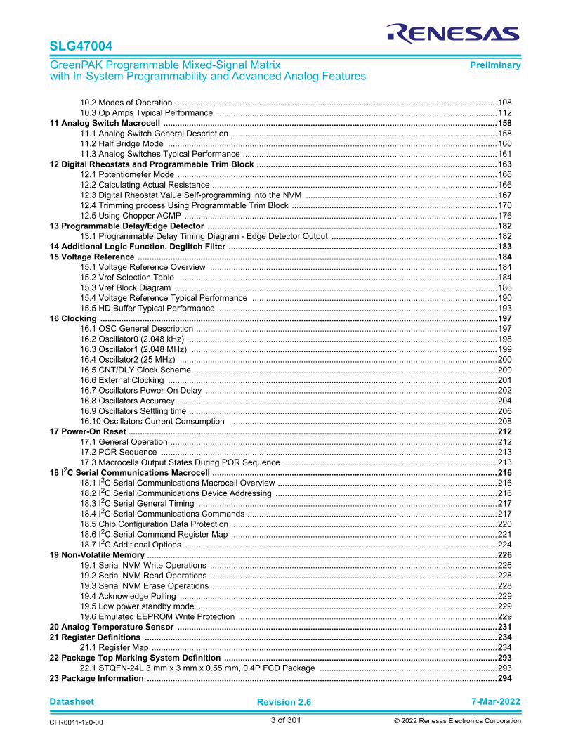
1 Block Diagram
Figure 1: Block Diagram
ChopperACMP
Low Power Vref TemperatureSensor
Analog Switch 1/ Current Sink Mode
3-bit LUT3_4 or DFF7
ProgrammableDelay or Edge
Detect
Prog,OA0
Filter with Edge Detect
Combination Function Macrocells
2-bit LUT2_0 or DFF0
2-bit LUT2_2 or DFF2
2-bit LUT2_1 or DFF1
3bit LUT3_0 or DFF3
3-bit LUT3_2 or DFF5
3-bit LUT3_1 or DFF4
3-bit LUT3_5 or DFF8
PORI2C Serial
Communication
3-bit LUT3_7 /DFF11+8bit
CNT/DLY1
3-bit LUT3_8 /DFF12+8bit
CNT/DLY2
3-bit LUT3_9 /DFF13+8bit
CNT/DLY3
3-bit LUT3_11 /DFF15+8bit
CNT/DLY5
3-bit LUT3_12/DFF16+8bit
CNT/DLY6
2-bit LUT2_3 or PGen
3-bit LUT3_3 or DFF6
3-bit LUT3_10 /DFF14+8bit
CNT/DLY4
4-bit LUT4_1 /DFF17+
16bitCNT/DLY0
VDDA
OA0+
OA0-
OA0_OUT
RH0_A
In-SystemProgrammability
Multiple Time Programmable
Memory
RH0_B
OA1_OUT IO6
IO5
IO4
IO3
IO2
AGND OA1- OA1+
RH1_A RH1_B SCL SDA
IO1
Oscillators
25MHz
2.048kHz
2.048MHz
2K bitsEEPROM Emulation
Multi-Function Macrocells
IO7
IO0 GND
VDD
Prog,OA1
4-bit LUT4_0
or DFF10
Analog Switch 0/Voltage Regulator Mode
3-bit LUT3_13 or Pipe Delay or Ripple CNT
3-bit LUT3_6 or DFF9
Int.OA
ProgrammableTrim Block
1024 Position Rheostat
1024 Position Rheostat
HDBuffer
ACMP0L ACMP1L

Datasheet 7-Mar-2022
CFR0011-120-00
Revision 2.6
13 of 301 © 2022 Renesas Electronics Corporation
SLG47004
GreenPAK Programmable Mixed-Signal Matrix with In-System Programmability and Advanced Analog Features
Preliminary
2 Pinout
2.1 PIN CONFIGURATION - STQFN-24L
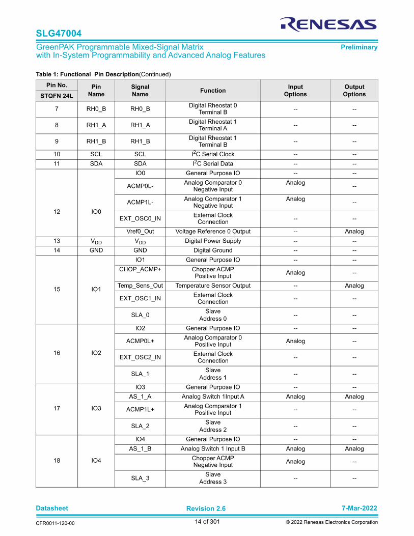
Table 1: Functional Pin Description
Pin No. Pin
Name
Signal
NameFunction
Input
Options
Output
OptionsSTQFN 24L
1 VDDA VDDA Analog Power Supply -- --
2 AGND AGND Analog Ground -- --
3 OA0- OA0- Op Amp0Inverting Input Analog --
4 OA0+ OA0+ Op Amp0Non-Inverting Input Analog --
5OA0_OUT
OA0_OUT Op Amp0 Output -- Analog
ACMP0L+ Analog Comparator 0 Positive In-put Analog --
6 RH0_A RH0_A Digital Rheostat 0 Terminal A -- --
Pin # Signal Name Pin Functions
1 VDDA Analog Power Supply
2 AGND Analog Ground
3 OA0- Op Amp0 Inverting Input
4 OA0+ Op Amp0 Non-Inverting Input
5 OA0_OUT Op Amp0_OUT/ACMP0L+ /
6 RH0_A Digital Rheostat 0 Terminal A
7 RH0_B Digital Rheostat 0 Terminal B
8 RH1_A Digital Rheostat 1 Terminal A
9 RH1_B Digital Rheostat 1 Terminal B
10 SCL I2C_SCL
11 SDA I2C_SDA
12 IO0GPIO, ACMP0L-, ACMP1L-, EXT_OSC0_IN, Vref0_Out or Temp_Sens_Out
13 VDD Digital Power Supply
14 GND Digital Ground
15 IO1 GPIO, Chop_ACMP+, Vref1_OUT orTemp_Sens_Out, EXT_OSC1_IN or SLA_0
16 IO2 GPIO, ACMP0L+, EXT_OSC2_IN, SLA_1
17 IO3 GPIO, AS_1_A, ACMP1L+ or SLA_2
18 IO4 GPIO, AS_1_B, Chop_ACMP-or SLA_3
19 IO5 GPIO, AS_0_B
20 IO6 GPIO, AS_0_A, HD_Buff_Out, In Amp_Vref
21 I0 GPI, In Amp_OUT
22 OA1_OUT Op Amp1_OUT, ACMP1L+
23 OA1+ Op Amp1 Non-inverting Input
24 OA1- Op Amp1 Inverting Input
Legend:
IO2
IO3
IO4
OA0+
OA0-
2
3
4
16
17
18
AGND
VDDA 1
RH0_A
OA0_OUT 5
6
GND
IO1
14
15
VDD13
RH
1_B
RH
1_A
8 9
SC
L
10
OA
1+
OA
1_O
UT
2223
OA
1-
24
STQFN-24
I0
21
RH
0_B
7
(Top View)
SD
A
IO0
11 12
20 19
ACMPx+: ACMPx Positive InputACMPx-: ACMPx Negative InputSCL: I2C Clock InputSDA: I2C Data Input/OutputVrefx: Voltage Reference OutputSLA: Slave Address
IO6
IO5
Datasheet 7-Mar-2022
CFR0011-120-00
Revision 2.6
14 of 301 © 2022 Renesas Electronics Corporation
SLG47004
GreenPAK Programmable Mixed-Signal Matrix with In-System Programmability and Advanced Analog Features
Preliminary
7 RH0_B RH0_B Digital Rheostat 0 Terminal B -- --
8 RH1_A RH1_A Digital Rheostat 1Terminal A -- --
9 RH1_B RH1_B Digital Rheostat 1Terminal B -- --
10 SCL SCL I2C Serial Clock -- --
11 SDA SDA I2C Serial Data -- --
12 IO0
IO0 General Purpose IO -- --
ACMP0L- Analog Comparator 0Negative Input
Analog --
ACMP1L- Analog Comparator 1Negative Input
Analog --
EXT_OSC0_IN External ClockConnection -- --
Vref0_Out Voltage Reference 0 Output -- Analog
13 VDD VDD Digital Power Supply -- --
14 GND GND Digital Ground -- --
15 IO1
IO1 General Purpose IO -- --
CHOP_ACMP+ Chopper ACMPPositive Input Analog --
Temp_Sens_Out Temperature Sensor Output -- Analog
EXT_OSC1_IN External ClockConnection -- --
SLA_0Slave
Address 0-- --
16 IO2
IO2 General Purpose IO -- --
ACMP0L+ Analog Comparator 0Positive Input Analog --
EXT_OSC2_IN External ClockConnection -- --
SLA_1Slave
Address 1-- --
17 IO3
IO3 General Purpose IO -- --
AS_1_A Analog Switch 1Input A Analog Analog
ACMP1L+ Analog Comparator 1Positive Input -- --
SLA_2Slave
Address 2-- --
18 IO4
IO4 General Purpose IO -- --
AS_1_B Analog Switch 1 Input B Analog Analog
Chopper ACMPNegative Input Analog --
SLA_3Slave
Address 3-- --
Table 1: Functional Pin Description(Continued)
Pin No. Pin
Name
Signal
NameFunction
Input
Options
Output
OptionsSTQFN 24L
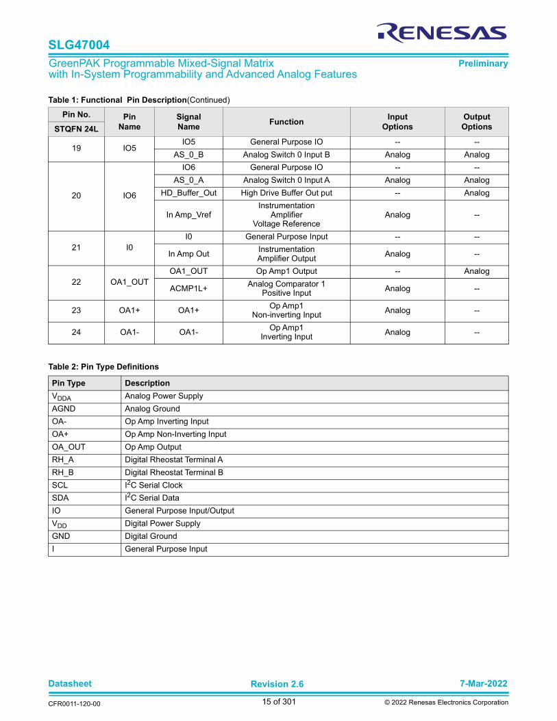
Datasheet 7-Mar-2022
CFR0011-120-00
Revision 2.6
15 of 301 © 2022 Renesas Electronics Corporation
SLG47004
GreenPAK Programmable Mixed-Signal Matrix with In-System Programmability and Advanced Analog Features
Preliminary
19 IO5IO5 General Purpose IO -- --
AS_0_B Analog Switch 0 Input B Analog Analog
20 IO6
IO6 General Purpose IO -- --
AS_0_A Analog Switch 0 Input A Analog Analog
HD_Buffer_Out High Drive Buffer Out put -- Analog
In Amp_VrefInstrumentation
AmplifierVoltage Reference
Analog --
21 I0I0 General Purpose Input -- --
In Amp Out InstrumentationAmplifier Output Analog --
22 OA1_OUTOA1_OUT Op Amp1 Output -- Analog
ACMP1L+ Analog Comparator 1Positive Input Analog --
23 OA1+ OA1+ Op Amp1Non-inverting Input Analog --
24 OA1- OA1- Op Amp1Inverting Input Analog --
Table 2: Pin Type Definitions
Pin Type Description
VDDA Analog Power Supply
AGND Analog Ground
OA- Op Amp Inverting Input
OA+ Op Amp Non-Inverting Input
OA_OUT Op Amp Output
RH_A Digital Rheostat Terminal A
RH_B Digital Rheostat Terminal B
SCL I2C Serial Clock
SDA I2C Serial Data
IO General Purpose Input/Output
VDD Digital Power Supply
GND Digital Ground
I General Purpose Input
Table 1: Functional Pin Description(Continued)
Pin No. Pin
Name
Signal
NameFunction
Input
Options
Output
OptionsSTQFN 24L
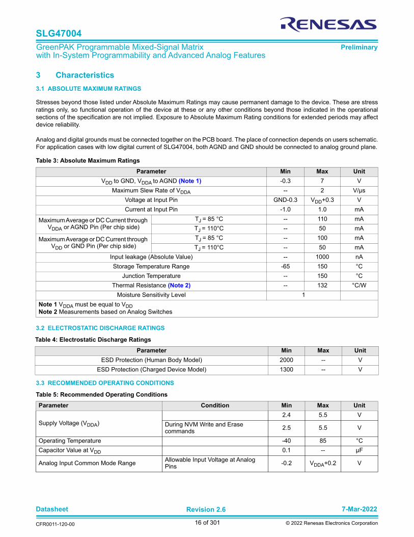
Datasheet 7-Mar-2022
CFR0011-120-00
Revision 2.6
16 of 301 © 2022 Renesas Electronics Corporation
SLG47004
GreenPAK Programmable Mixed-Signal Matrix with In-System Programmability and Advanced Analog Features
Preliminary
3 Characteristics
3.1 ABSOLUTE MAXIMUM RATINGS
Stresses beyond those listed under Absolute Maximum Ratings may cause permanent damage to the device. These are stressratings only, so functional operation of the device at these or any other conditions beyond those indicated in the operationalsections of the specification are not implied. Exposure to Absolute Maximum Rating conditions for extended periods may affectdevice reliability.
Analog and digital grounds must be connected together on the PCB board. The place of connection depends on users schematic.For application cases with low digital current of SLG47004, both AGND and GND should be connected to analog ground plane.
3.2 ELECTROSTATIC DISCHARGE RATINGS
3.3 RECOMMENDED OPERATING CONDITIONS
Table 3: Absolute Maximum Ratings
Parameter Min Max Unit
VDD to GND, VDDA to AGND (Note 1) -0.3 7 V
Maximum Slew Rate of VDDA -- 2 V/µs
Voltage at Input Pin GND-0.3 VDD+0.3 V
Current at Input Pin -1.0 1.0 mA
Maximum Average or DC Current through VDDA or AGND Pin (Per chip side)
TJ = 85 °C -- 110 mA
TJ = 110°C -- 50 mA
Maximum Average or DC Current through VDD or GND Pin (Per chip side)
TJ = 85 °C -- 100 mA
TJ = 110°C -- 50 mA
Input leakage (Absolute Value) -- 1000 nA
Storage Temperature Range -65 150 °C
Junction Temperature -- 150 °C
Thermal Resistance (Note 2) -- 132 °C/W
Moisture Sensitivity Level 1
Note 1 VDDA must be equal to VDDNote 2 Measurements based on Analog Switches
Table 4: Electrostatic Discharge Ratings
Parameter Min Max Unit
ESD Protection (Human Body Model) 2000 -- V
ESD Protection (Charged Device Model) 1300 -- V
Table 5: Recommended Operating Conditions
Parameter Condition Min Max Unit
Supply Voltage (VDDA)2.4 5.5 V
During NVM Write and Erase commands 2.5 5.5 V
Operating Temperature -40 85 °C
Capacitor Value at VDD 0.1 -- µF
Analog Input Common Mode Range Allowable Input Voltage at Analog Pins -0.2 VDDA+0.2 V

Datasheet 7-Mar-2022
CFR0011-120-00
Revision 2.6
17 of 301 © 2022 Renesas Electronics Corporation
SLG47004
GreenPAK Programmable Mixed-Signal Matrix with In-System Programmability and Advanced Analog Features
Preliminary
3.4 ELECTRICAL CHARACTERISTICS
Table 6: EC at T = -40 °C to +85 °C, VDD = 2.4 V to 5.5 V Unless Otherwise Noted
Parameter Description Condition Min Typ Max Unit
VIH HIGH-Level Input Voltage
Logic Input (Note 1)0.7xVDD
-- VDD+ 0.3 V
Logic Input with Schmitt Trigger 0.8xVDD
-- VDD+ 0.3 V
Low-Level Logic Input (Note 1) 1.25 -- VDD+ 0.3 V
VIL LOW-Level Input Voltage
Logic Input (Note 1)GND-
0.3 -- 0.3xVDD
V
Logic Input with Schmitt Trigger GND-0.3 -- 0.2x
VDDV
Low-Level Logic Input (Note 1)GND-
0.3 -- 0.5 V
VHYSSchmitt Trigger Hysteresis Voltage
VDD = 2.5 V +/- 8 % 0.30 0.43 0.58 V
VDD = 3.3 V +/- 10 % 0.34 0.46 0.60 V
VDD = 5 V +/- 10 % 0.45 0.58 0.77 V
VO
Maximal Voltage Applied to any PIN in High Impedance State
-- -- VDD+0.3 V
VOH HIGH-Level Output Voltage
Push-Pull, 1x Drive, IOH = 1 mA, VDD = 2.4 V (Note 1)
2.282 -- -- V
Push-Pull, 1x Drive, IOH = 1 mA, VDD = 2.5 V (Note 1)
2.387 -- -- V
Push-Pull, 1x Drive, IOH = 1 mA, VDD = 2.7 V (Note 1)
2.597 -- -- V
Push-Pull, 1x Drive, IOH = 3 mA, VDD = 3.0 V (Note 1)
2.709 -- -- V
Push-Pull, 1x Drive, IOH = 3 mA, VDD = 3.3 V (Note 1)
3.037 -- -- V
Push-Pull, 1x Drive, IOH = 3 mA, VDD = 3.6 V (Note 1)
3.359 -- -- V
Push-Pull, 1x Drive, IOH = 5 mA, VDD = 4.5 V (Note 1)
4.161 -- -- V
Push-Pull, 1x Drive, IOH = 5 mA, VDD = 5.0 V (Note 1)
4.687 -- -- V
Push-Pull, 1x Drive, IOH = 5 mA, VDD = 5.5 V (Note 1)
5.213 -- -- V
Push-Pull, 2x Drive, IOH = 1 mA, VDD = 2.4 V (Note 1)
2.342 -- -- V
Push-Pull, 2x Drive, IOH = 1 mA, VDD = 2.5 V (Note 1)
2.445 -- -- V
Push-Pull, 2x Drive, IOH = 1 mA, VDD = 2.7 V (Note 1)
2.649 -- -- V
Push-Pull, 2x Drive, IOH = 3 mA, VDD = 3.0 V (Note 1)
2.859 -- -- V
Push-Pull, 2x Drive, IOH = 3 mA,VDD = 3.3 V (Note 1)
3.171 -- -- V
Push-Pull, 2x Drive, IOH = 3 mA, VDD = 3.6 V (Note 1)
3.481 -- -- V

Datasheet 7-Mar-2022
CFR0011-120-00
Revision 2.6
18 of 301 © 2022 Renesas Electronics Corporation
SLG47004
GreenPAK Programmable Mixed-Signal Matrix with In-System Programmability and Advanced Analog Features
Preliminary
VOH HIGH-Level Output Voltage
Push-Pull, 2x Drive, IOH = 5 mA,VDD = 4.5 V (Note 1)
4.333 -- -- V
Push-Pull, 2x Drive, IOH = 5 mA, VDD = 5.0 V (Note 1)
4.845 -- -- V
Push-Pull, 2x Drive, IOH = 5 mA, VDD = 5.5 V (Note 1)
5.356 -- -- V
VOL LOW-Level Output Voltage
Push-Pull, 1x Drive, IOL= 1 mA, VDD = 2.4 V (Note 1)
-- -- 0.085 V
Push-Pull, 1x Drive, IOL= 1 mA, VDD = 2.5 V (Note 1)
-- -- 0.082 V
Push-Pull, 1x Drive, IOL= 1 mA, VDD = 2.7 V (Note 1)
-- -- 0.077 V
Push-Pull, 1x Drive, IOL = 3 mA,VDD = 3.0 V (Note 1)
-- -- 0.218 V
Push-Pull, 1x Drive, IOL = 3 mA,VDD = 3.3 V (Note 1)
-- -- 0.202 V
Push-Pull, 1x Drive, IOL = 3 mA,VDD = 3.6 V (Note 1)
-- -- 0.190 V
Push-Pull, 1x Drive, IOL= 5 mA, VDD = 4.5 V (Note 1)
-- -- 0.277 V
Push-Pull, 1x Drive, IOL= 5 mA, VDD = 5.0 V (Note 1)
-- -- 0.260 V
Push-Pull, 1x Drive, IOL= 5 mA, VDD = 5.5 V (Note 1)
-- -- 0.245 V
Push-Pull, 2x Drive, IOL= 1 mA, VDD = 2.4 V (Note 1)
-- -- 0.043 V
Push-Pull, 2x Drive, IOL = 1 mA, VDD = 2.5 V (Note 1)
-- -- 0.042 V
Push-Pull, 2x Drive, IOL = 1 mA, VDD = 2.7 V (Note 1)
-- -- 0.039 V
Push-Pull, 2x Drive, IOL= 3 mA, VDD = 3.0 V (Note 1)
-- -- 0.109 V
Push-Pull, 2x Drive, IOL= 3 mA, VDD = 3.3 V (Note 1)
-- -- 0.102 V
Push-Pull, 2x Drive, IOL= 3 mA, VDD = 3.6 V (Note 1)
-- -- 0.096 V
Push-Pull, 2x Drive, IOL = 5 mA, VDD = 4.5 V (Note 1)
-- -- 0.143 V
Push-Pull, 2x Drive, IOL = 5 mA, VDD = 5.0 V (Note 1)
-- -- 0.136 V
Push-Pull, 2x Drive, IOL = 5 mA, VDD = 5.5 V (Note 1)
-- -- 0.127 V
NMOS OD, 1x Drive, IOL= 1 mA, VDD = 2.4 V (Note 1)
-- -- 0.035 V
NMOS OD, 1x Drive, IOL = 1 mA, VDD = 2.5 V (Note 1)
-- -- 0.034 V
NMOS OD, 1x Drive, IOL = 1 mA, VDD = 2.7 V (Note 1)
-- -- 0.032 V
NMOS OD, 1x Drive, IOL = 3 mA, VDD = 3.0 V (Note 1)
-- -- 0.088 V
Table 6: EC at T = -40 °C to +85 °C, VDD = 2.4 V to 5.5 V Unless Otherwise Noted(Continued)
Parameter Description Condition Min Typ Max Unit
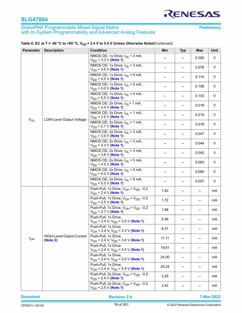
Datasheet 7-Mar-2022
CFR0011-120-00
Revision 2.6
19 of 301 © 2022 Renesas Electronics Corporation
SLG47004
GreenPAK Programmable Mixed-Signal Matrix with In-System Programmability and Advanced Analog Features
Preliminary
VOL LOW-Level Output Voltage
NMOS OD, 1x Drive, IOL = 3 mA, VDD = 3.3 V (Note 1)
-- -- 0.082 V
NMOS OD, 1x Drive, IOL = 3 mA, VDD = 3.6 V (Note 1)
-- -- 0.078 V
NMOS OD, 1x Drive, IOL = 5 mA, VDD = 4.5 V (Note 1)
-- -- 0.114 V
NMOS OD, 1x Drive, IOL = 5 mA, VDD = 5.0 V (Note 1)
-- -- 0.108 V
NMOS OD, 1x Drive, IOL = 5 mA, VDD = 5.5 V (Note 1)
-- -- 0.103 V
NMOS OD, 2x Drive, IOL= 1 mA, VDD = 2.4 V (Note 1)
-- -- 0.019 V
NMOS OD, 2x Drive, IOL = 1 mA, VDD = 2.5 V (Note 1)
-- -- 0.019 V
NMOS OD, 2x Drive, IOL = 1 mA, VDD = 2.7 V (Note 1)
-- -- 0.018 V
NMOS OD, 2x Drive, IOL = 3 mA, VDD = 3.0 V (Note 1)
-- -- 0.047 V
NMOS OD, 2x Drive, IOL = 3 mA, VDD = 3.3 V (Note 1)
-- -- 0.044 V
NMOS OD, 2x Drive, IOL = 3 mA, VDD = 3.6 V (Note 1)
-- -- 0.042 V
NMOS OD, 2x Drive, IOL = 5 mA, VDD = 4.5 V (Note 1)
-- -- 0.063 V
NMOS OD, 2x Drive, IOL = 5 mA, VDD = 5.0 V (Note 1)
-- -- 0.060 V
NMOS OD, 2x Drive, IOL = 5 mA, VDD = 5.5 V (Note 1)
-- -- 0.057 V
IOHHIGH-Level Output Current (Note 2)
Push-Pull, 1x Drive, VOH = VDD - 0.2VDD = 2.4 V (Note 1)
1.63 -- -- mA
Push-Pull, 1x Drive, VOH = VDD - 0.2VDD = 2.5 V (Note 1)
1.72 -- -- mA
Push-Pull, 1x Drive, VOH = VDD - 0.2VDD = 2.7 V (Note 1)
1.88 -- -- mA
Push-Pull, 1x Drive, VOH = 2.4 V, VDD = 3.0 V (Note 1)
5.48 -- -- mA
Push-Pull, 1x Drive, VOH = 2.4 V, VDD = 3.3 V (Note 1)
8.31 -- -- mA
Push-Pull, 1x Drive, VOH = 2.4 V, VDD = 3.6 V (Note 1)
11.11 -- -- mA
Push-Pull, 1x Drive, VOH = 2.4 V, VDD = 4.5 V (Note 1)
19.61 -- -- mA
Push-Pull, 1x Drive, VOH = 2.4 V, VDD = 5.0 V (Note 1)
24.00 -- -- mA
Push-Pull, 1x Drive, VOH = 2.4 V, VDD = 5.5 V (Note 1)
29.24 -- -- mA
Push-Pull, 2x Drive, VOH = VDD - 0.2 VDD = 2.4 V (Note 1)
3.25 -- -- mA
Push-Pull, 2x Drive, VOH = VDD - 0.2 VDD = 2.5 V (Note 1)
3.42 -- -- mA
Table 6: EC at T = -40 °C to +85 °C, VDD = 2.4 V to 5.5 V Unless Otherwise Noted(Continued)
Parameter Description Condition Min Typ Max Unit

Datasheet 7-Mar-2022
CFR0011-120-00
Revision 2.6
20 of 301 © 2022 Renesas Electronics Corporation
SLG47004
GreenPAK Programmable Mixed-Signal Matrix with In-System Programmability and Advanced Analog Features
Preliminary
IOHHIGH-Level Output Current (Note 2)
Push-Pull, 2x Drive, VOH = VDD - 0.2 VDD = 2.7 V (Note 1)
3.73 -- -- mA
Push-Pull, 2x Drive, VOH = 2.4 V, VDD = 3.0 V (Note 1)
10.84 -- -- mA
Push-Pull, 2x Drive, VOH = 2.4 V, VDD = 3.3 V (Note 1)
16.34 -- -- mA
Push-Pull, 2x Drive, VOH = 2.4 V, VDD = 3.6 V (Note 1)
21.83 -- -- mA
Push-Pull, 2x Drive, VOH = 2.4 V, VDD = 4.5 V (Note 1)
38.34 -- -- mA
Push-Pull, 2x Drive, VOH = 2.4 V, VDD = 5.0 V (Note 1)
47.07 -- -- mA
Push-Pull, 2x Drive, VOH = 2.4 V, VDD = 5.5 V (Note 1)
56.68 -- -- mA
IOLLOW-Level Output Current (Note 2)
Push-Pull, 1x Drive, VOL = 0.15 V, VDD = 2.4 V (Note 1)
1.67 -- -- mA
Push-Pull, 1x Drive, VOL = 0.15 V, VDD = 2.5 V (Note 1)
1.74 -- -- mA
Push-Pull, 1x Drive, VOL = 0.15 V, VDD = 2.7 V (Note 1)
1.85 -- -- mA
Push-Pull, 1x Drive, VOL = 0.4 V,VDD = 3.0 V (Note 1)
5.07 -- -- mA
Push-Pull, 1x Drive, VOL = 0.4 V,VDD = 3.3 V (Note 1)
5.48 -- -- mA
Push-Pull, 1x Drive, VOL = 0.4 V,VDD = 3.6 V (Note 1)
5.85 -- -- mA
Push-Pull, 1x Drive, VOL = 0.4 V, VDD = 4.5 V (Note 1)
6.81 -- -- mA
Push-Pull, 1x Drive, VOL = 0.4 V, VDD = 5.0 V (Note 1)
7.27 -- -- mA
Push-Pull, 1x Drive, VOL = 0.4 V, VDD = 5.5 V (Note 1)
7.72 -- -- mA
Push-Pull, 2x Drive, VOL = 0.15 V, VDD = 2.4 V (Note 1)
3.27 -- -- mA
Push-Pull, 2x Drive, VOL = 0.15 V, VDD = 2.5 V (Note 1)
3.39 -- -- mA
Push-Pull, 2x Drive, VOL = 0.15 V, VDD = 2.7 V (Note 1)
3.61 -- -- mA
Push-Pull, 2x Drive, VOL = 0.4 V, VDD = 3.0 (Note 1)
9.85 -- -- mA
Push-Pull, 2x Drive, VOL = 0.4 V, VDD = 3.3 (Note 1)
10.63 -- -- mA
Push-Pull, 2x Drive, VOL = 0.4 V, VDD = 3.6 (Note 1)
11.33 -- -- mA
Push-Pull, 2x Drive, VOL = 0.4 V, VDD = 4.5 (Note 1)
13.06 -- -- mA
Push-Pull, 2x Drive, VOL = 0.4 V, VDD = 5.0 (Note 1)
13.79 -- -- mA
Table 6: EC at T = -40 °C to +85 °C, VDD = 2.4 V to 5.5 V Unless Otherwise Noted(Continued)
Parameter Description Condition Min Typ Max Unit
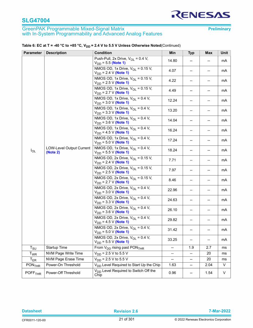
Datasheet 7-Mar-2022
CFR0011-120-00
Revision 2.6
21 of 301 © 2022 Renesas Electronics Corporation
SLG47004
GreenPAK Programmable Mixed-Signal Matrix with In-System Programmability and Advanced Analog Features
Preliminary
IOLLOW-Level Output Current (Note 2)
Push-Pull, 2x Drive, VOL = 0.4 V, VDD = 5.5 (Note 1)
14.80 -- -- mA
NMOS OD, 1x Drive, VOL = 0.15 V, VDD = 2.4 V (Note 1)
4.07 -- -- mA
NMOS OD, 1x Drive, VOL = 0.15 V, VDD = 2.5 V (Note 1)
4.22 -- -- mA
NMOS OD, 1x Drive, VOL = 0.15 V, VDD = 2.7 V (Note 1)
4.49 -- -- mA
NMOS OD, 1x Drive, VOL = 0.4 V, VDD = 3.0 V (Note 1)
12.24 -- -- mA
NMOS OD, 1x Drive, VOL = 0.4 V, VDD = 3.3 V (Note 1)
13.20 -- -- mA
NMOS OD, 1x Drive, VOL = 0.4 V, VDD = 3.6 V (Note 1)
14.04 -- -- mA
NMOS OD, 1x Drive, VOL = 0.4 V, VDD = 4.5 V (Note 1)
16.24 -- -- mA
NMOS OD, 1x Drive, VOL = 0.4 V, VDD = 5.0 V (Note 1)
17.24 -- -- mA
NMOS OD, 1x Drive, VOL = 0.4 V, VDD = 5.5 V (Note 1)
18.24 -- -- mA
NMOS OD, 2x Drive, VOL = 0.15 V, VDD = 2.4 V (Note 1)
7.71 -- -- mA
NMOS OD, 2x Drive, VOL = 0.15 V, VDD = 2.5 V (Note 1)
7.97 -- -- mA
NMOS OD, 2x Drive, VOL = 0.15 V, VDD = 2.7 V (Note 1)
8.46 -- -- mA
NMOS OD, 2x Drive, VOL = 0.4 V, VDD = 3.0 V (Note 1)
22.96 -- -- mA
NMOS OD, 2x Drive, VOL = 0.4 V, VDD = 3.3 V (Note 1)
24.63 -- -- mA
NMOS OD, 2x Drive, VOL = 0.4 V, VDD = 3.6 V (Note 1)
26.10 -- -- mA
NMOS OD, 2x Drive, VOL = 0.4 V, VDD = 4.5 V (Note 1)
29.82 -- -- mA
NMOS OD, 2x Drive, VOL = 0.4 V, VDD = 5.0 V (Note 1)
31.42 -- -- mA
NMOS OD, 2x Drive, VOL = 0.4 V, VDD = 5.5 V (Note 1)
33.25 -- -- mA
TSU Startup Time From VDD rising past PONTHR -- 1.9 2.7 ms
TWR NVM Page Write Time VDD = 2.5 V to 5.5 V -- -- 20 ms
TER NVM Page Erase Time VDD = 2.5 V to 5.5 V -- -- 20 ms
PONTHR Power-On Threshold VDD Level Required to Start Up the Chip 1.63 -- 2.04 V
POFFTHR Power-Off Threshold VDD Level Required to Switch Off the Chip 0.96 -- 1.54 V
Table 6: EC at T = -40 °C to +85 °C, VDD = 2.4 V to 5.5 V Unless Otherwise Noted(Continued)
Parameter Description Condition Min Typ Max Unit

Datasheet 7-Mar-2022
CFR0011-120-00
Revision 2.6
22 of 301 © 2022 Renesas Electronics Corporation
SLG47004
GreenPAK Programmable Mixed-Signal Matrix with In-System Programmability and Advanced Analog Features
Preliminary
3.5 I2C PINS CHARACTERISTICS
RPULLPull-up or Pull-down Resistance
1 M for Pull-up: VIN = GND; for Pull-down: VIN = VDD (Note 1)
-- 1 -- MΩ
100 k for Pull-up: VIN = GND;for Pull-down: VIN = VDD (Note 1)
-- 100 -- kΩ
10 k For Pull-up: VIN = GND;for Pull-down: VIN = VDD (Note 1)
-- 10 -- kΩ
CIN Input Capacitance
PINs 10, 11 -- 2.9 -- pF
PIN 12 -- 3.6 -- pF
PINs 15, 16 -- 3.8 -- pF
PINs 17, 18, 19 -- 10.2 -- pF
PIN 20 -- 27.8 -- pF
PIN 21 -- 5.7 -- pF
Note 1 No hysteresis.Note 2 DC or average current through any pin should not exceed value given in Absolute Maximum Conditions.
Table 7: EC of the I2C Pins for DI at T = -40 °C to +85 °C, VDD = 2.4 V to 5.5 V Unless Otherwise Noted
Parameter Description ConditionFast-Mode Fast-Mode Plus
UnitMin Max Min Max
VILLOW-level Input Voltage -0.5 0.3xVDD -0.5 0.3xVDD V
VIHHIGH-level Input Voltage 0.7xVDD 5.5 0.7xVDD 5.5 V
VHYSHysteresis of Schmitt Trigger Inputs 0.05xVDD -- 0.05xVDD -- V
VOL1LOW-Level Output Voltage 1
(Open-Drain) at 3 mA sink currentVDD > 2 V
0 0.4 0 0.4 V
VOL2LOW-Level Output Voltage 2
(Open-Drain) at 2 mA sink currentVDD ≤ 2 V
0 0.2xVDD 0 0.2xVDD V
IOLLOW-Level Output Current (Note 1)
VOL = 0.4 V, VDD = 2.4 V 3 -- 16.75 -- mA
VOL = 0.4 V, VDD = 3.0 V 3 -- 20 -- mA
VOL = 0.4 V, VDD = 4.5 V 3 -- 20 -- mA
VOL= 0.6 V 6 -- -- -- mA
tof
Output Fall Time from VIHmin to VILmax (Note 1)
14x(VDD/5.5 V) 250 10x
(VDD/5.5 V) 120 ns
tSP
Pulse Width of Spikes that must be suppressed by the Input Filter
0 50 0 50 ns
IiInput Current (each IO Pin) 0.1xVDD < VI < 0.9xVDDmax -10 +10 -10 +10 µA
CiCapacitance (each IO Pin) -- 10 -- 10 pF
Table 6: EC at T = -40 °C to +85 °C, VDD = 2.4 V to 5.5 V Unless Otherwise Noted(Continued)
Parameter Description Condition Min Typ Max Unit
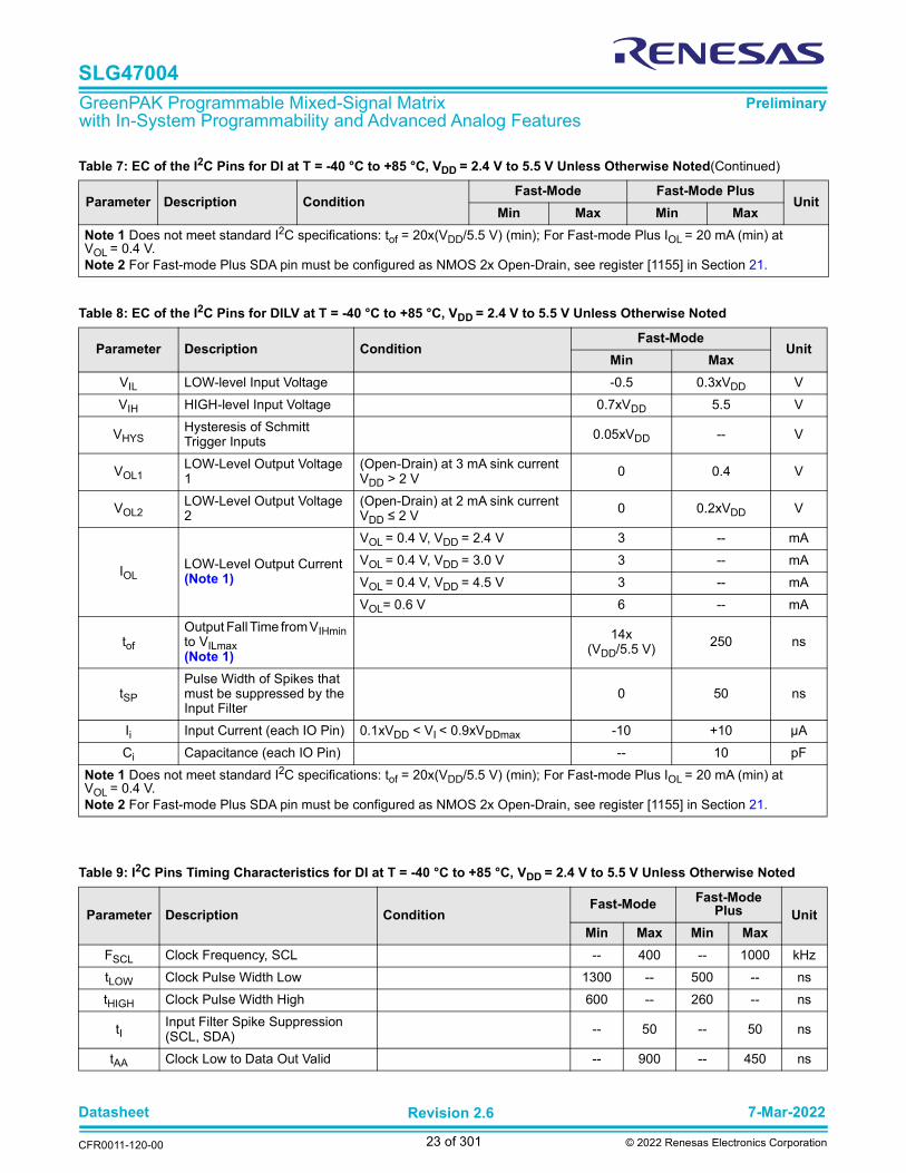
Datasheet 7-Mar-2022
CFR0011-120-00
Revision 2.6
23 of 301 © 2022 Renesas Electronics Corporation
SLG47004
GreenPAK Programmable Mixed-Signal Matrix with In-System Programmability and Advanced Analog Features
Preliminary
Note 1 Does not meet standard I2C specifications: tof = 20x(VDD/5.5 V) (min); For Fast-mode Plus IOL = 20 mA (min) atVOL = 0.4 V.Note 2 For Fast-mode Plus SDA pin must be configured as NMOS 2x Open-Drain, see register [1155] in Section 21.
Table 8: EC of the I2C Pins for DILV at T = -40 °C to +85 °C, VDD = 2.4 V to 5.5 V Unless Otherwise Noted
Parameter Description ConditionFast-Mode
UnitMin Max
VIL LOW-level Input Voltage -0.5 0.3xVDD V
VIH HIGH-level Input Voltage 0.7xVDD 5.5 V
VHYSHysteresis of Schmitt Trigger Inputs 0.05xVDD -- V
VOL1LOW-Level Output Voltage 1
(Open-Drain) at 3 mA sink currentVDD > 2 V 0 0.4 V
VOL2LOW-Level Output Voltage 2
(Open-Drain) at 2 mA sink currentVDD ≤ 2 V 0 0.2xVDD V
IOLLOW-Level Output Current (Note 1)
VOL = 0.4 V, VDD = 2.4 V 3 -- mA
VOL = 0.4 V, VDD = 3.0 V 3 -- mA
VOL = 0.4 V, VDD = 4.5 V 3 -- mA
VOL= 0.6 V 6 -- mA
tof
Output Fall Time from VIHmin to VILmax (Note 1)
14x(VDD/5.5 V) 250 ns
tSP
Pulse Width of Spikes that must be suppressed by the Input Filter
0 50 ns
Ii Input Current (each IO Pin) 0.1xVDD < VI < 0.9xVDDmax -10 +10 µA
Ci Capacitance (each IO Pin) -- 10 pF
Note 1 Does not meet standard I2C specifications: tof = 20x(VDD/5.5 V) (min); For Fast-mode Plus IOL = 20 mA (min) atVOL = 0.4 V.Note 2 For Fast-mode Plus SDA pin must be configured as NMOS 2x Open-Drain, see register [1155] in Section 21.
Table 9: I2C Pins Timing Characteristics for DI at T = -40 °C to +85 °C, VDD = 2.4 V to 5.5 V Unless Otherwise Noted
Parameter Description ConditionFast-Mode
Fast-Mode Plus Unit
Min Max Min Max
FSCL Clock Frequency, SCL -- 400 -- 1000 kHz
tLOW Clock Pulse Width Low 1300 -- 500 -- ns
tHIGH Clock Pulse Width High 600 -- 260 -- ns
tIInput Filter Spike Suppression (SCL, SDA) -- 50 -- 50 ns
tAA Clock Low to Data Out Valid -- 900 -- 450 ns
Table 7: EC of the I2C Pins for DI at T = -40 °C to +85 °C, VDD = 2.4 V to 5.5 V Unless Otherwise Noted(Continued)
Parameter Description ConditionFast-Mode Fast-Mode Plus
UnitMin Max Min Max

Datasheet 7-Mar-2022
CFR0011-120-00
Revision 2.6
24 of 301 © 2022 Renesas Electronics Corporation
SLG47004
GreenPAK Programmable Mixed-Signal Matrix with In-System Programmability and Advanced Analog Features
Preliminary
tBUFBus Free Time between Stop and Start 1300 -- 500 -- ns
tHD_STA Start Hold Time 600 -- 260 -- ns
tSU_STA Start Set-up Time 600 -- 260 -- ns
tHD_DAT Data Hold Time 0 -- 0 -- ns
tSU_DAT Data Set-up Time 100 -- 50 -- ns
tR Inputs Rise Time -- 300 -- 120 ns
tF Inputs Fall Time -- 300 -- 120 ns
tSU_STD Stop Set-up Time 600 -- 260 -- ns
tDH Data Out Hold Time 50 -- 50 -- ns
Note 1 Timing diagram can be found in Figure 236.
Table 10: I2C Pins Timing Characteristics for DILV at T = -40 °C to +85 °C, VDD = 2.4 V to 5.5 V Unless Otherwise Noted
Parameter Description ConditionFast-Mode
UnitMin Max
FSCL Clock Frequency, SCL -- 400 kHz
tLOW Clock Pulse Width Low 1300 -- ns
tHIGH Clock Pulse Width High 600 -- ns
tIInput Filter Spike Suppression (SCL, SDA) -- 50 ns
tAA Clock Low to Data Out Valid -- 900 ns
tBUF Bus Free Time between Stop and Start 1300 -- ns
tHD_STA Start Hold Time 600 -- ns
tSU_STA Start Set-up Time 600 -- ns
tHD_DAT Data Hold Time (Note 1) 185 -- ns
tSU_DAT Data Set-up Time (Note 1) 335 -- ns
tR Inputs Rise Time -- 300 ns
tF Inputs Fall Time -- 300 ns
tSU_STD Stop Set-up Time 600 -- ns
tDH Data Out Hold Time 50 -- ns
Note 1 Does not meet standard I2C specifications: tHD_DAT = 0 ns (min), tSU_DAT = 100 ns (min) for Fast-modeNote 2 Timing diagram can be found in Figure 236.
Table 9: I2C Pins Timing Characteristics for DI at T = -40 °C to +85 °C, VDD = 2.4 V to 5.5 V Unless Otherwise
Parameter Description ConditionFast-Mode
Fast-Mode Plus Unit
Min Max Min Max

Datasheet 7-Mar-2022
CFR0011-120-00
Revision 2.6
25 of 301 © 2022 Renesas Electronics Corporation
SLG47004
GreenPAK Programmable Mixed-Signal Matrix with In-System Programmability and Advanced Analog Features
Preliminary
3.6 MACROCELLS CURRENT CONSUMPTION
Table 11: Typical Current Estimated for Each Macrocell at T = 25°C
Parameter Description Note VDD = 2.5 V VDD = 3.3 V VDD = 5.0 V Unit
I Current
Chip Quiescent, BG disabled 0.06 0.08 0.13 µA
Chip Quiescent, BG enabled 0.36 0.39 0.47 µA
OSC2 25 MHz, pre-divider = 1 40.78 49.64 70.54 µA
OSC2 25 MHz, pre-divider = 4 31.75 37.46 51.41 µA
OSC2 25 MHz, pre-divider = 8 29.96 35.06 47.62 µA
OSC1 2.048 MHz, pre-divider = 1 19.19 19.98 21.73 µA
OSC1 2.048 MHz, pre-divider = 4 18.50 19.05 20.26 µA
OSC1 2.048 MHz, pre-divider = 8 18.36 18.87 19.97 µA
OS00 2.048 kHz, pre-divider = 1 0.33 0.36 0.44 µA
OSC0 2.048 kHz, pre-divider = 4 0.33 0.36 0.44 µA
OSC0 2.048 kHz, pre-divider = 8 0.33 0.36 0.44 µA
Push-Pull 1x + 4 pF @ 2.048 kHz 0.38 0.44 0.55 µA
Push-Pull 1x + 4 pF @ 2.048 MHz 66.8 82.6 116.0 µA
Temperature Sensor, range 1 10.9 10.9 11.2 µA
Temperature Sensor, range 2 11.0 11.1 11.4 µA
One ACMPx_L (includes internal Vref) 6.1 6.2 6.4 µA
Two ACMPx_L (includes internal Vref) 8.4 8.5 8.8 µA
Op AmpX Quiescent Current(128 kHz bandwidth) 32.2 32.8 33.8 µA
Op AmpX Quiescent Current(8.192 MHz bandwidth) 607 611 613 µA
In Amp Quiescent Current (three Op Amps are ON, Rf1 = Rf2 = 50 kΩ, Rg =1 kΩ, 128 kHz bandwidth, Charge Pump - Disabled)
98 101 104 µA
In Amp Quiescent Current (three Op Amps are ON, Rf1 = Rf2 = 50 kΩ, Rg =1 kΩ, 128 kHz bandwidth, Charge Pump - Enabled)
75.2 77.5 80.8 µA
In Amp Quiescent Current (three Op Amps are ON, Rf1 = Rf2 = 50 kΩ, Rg =1 kΩ, 8.192 MHz bandwidth, Charge Pump - Disabled)
1819 1834 1844 µA
In Amp Quiescent Current (three Op Amps are ON, Rf1 = Rf2 = 50 kΩ, Rg =1 kΩ, 8.192 MHz bandwidth, Charge Pump - Enabled)
1225 1235 1245 µA
Chopper ACMP (with 2.048 kHz clock) 31.4 33.6 38.4 µA

Datasheet 7-Mar-2022
CFR0011-120-00
Revision 2.6
26 of 301 © 2022 Renesas Electronics Corporation
SLG47004
GreenPAK Programmable Mixed-Signal Matrix with In-System Programmability and Advanced Analog Features
Preliminary
3.7 TIMING CHARACTERISTICS
Table 12: Typical Delay Estimated for Each Macrocell at T = 25 °C
Parameter Description ConditionsVDD = 2.5 V VDD = 3.3 V VDD = 5.0 V Unit
Rising Falling Rising Falling Rising Falling
tpd Delay Digital Input to PP 1x 26 27 18 20 13 15 ns
tpd Delay Digital Input with Schmitt Trigger to PP 1x 27 28 19 21 15 15 ns
tpd Delay Digital Input to PP 2x 24 25 17 18 12 14 ns
tpd Delay Low Voltage Digital input to PP 1x 28 246 20 163 15 95 ns
tpd Delay Digital input to NMOS output -- 24 -- 18 -- 13 ns
tpd Delay Output enable from Pin, OE Hi-Zto 1 26 -- 19 -- 13 -- ns
tpd Delay Output enable from Pin, OE Hi-Zto 0 -- 26 -- 19 -- 14 ns
tpd Delay Digital input to 1x3-State(Z to 1)
26 -- 19 -- 13 -- ns
tpd Delay Digital input to x3-State(Z to 0)
-- 26 -- 17 -- 14 ns
tpd Delay Digital input to 2x3-State(Z to 1)
24 -- 17 -- 13 -- ns
tpd Delay Digital input to 2x3-State(Z to 0)
-- 24 -- 19 -- 12 ns
tpd Delay LUT2bt 17 17 12 12 8 8 ns
tpd Delay LUT3bit 19 20 13 14 9 10 ns
tpd Delay LUT4bit 20 21 15 14 9 10 ns
tpd Delay LATCH 25 25 17 18 12 12 ns
tpd Delay DFF 24 25 16 18 11 12 ns
tpd Delay CNT/DLY 107 107 77 74 48 70 ns
tw Width Edge detect 206 205 161 160 116 116 ns
tpd Delay Edge detect 19 20 13 13 8 8 ns
tpd Delay Edge detect Delayed 241 241 175 175 125 125 ns
tpd Delay Ripple Counter 45 60 32 44 22 31 ns
tpd Delay PGen 20 20 14 14 9 10 ns
tpd Delay Filter 177 177 121 121 77 78 ns
tpd Delay Inverter Filter 115 115 83 83 57 57 ns
tpd Delay Pipe Delay 36 37 25 26 17 18 ns
Table 13: Programmable Delay Expected Typical Delays and Widths at T = 25 °C
Parameter Description Note VDD = 2.5 V VDD = 3.3 V VDD = 5.0 V Unit
tw Pulse Width, 1 cell mode: (any) edge detect, edge detect output 223 163 118 ns
tw Pulse Width, 2 cell mode: (any) edge detect, edge detect output 444 324 233 ns
tw Pulse Width, 3 cell mode: (any) edge detect, edge detect output 663 484 347 ns
tw Pulse Width, 4 cell mode: (any) edge detect, edge detect output 882 643 461 ns
time1 Delay, 1 cell mode: (any) edge detect, edge detect output 18 12 8 ns
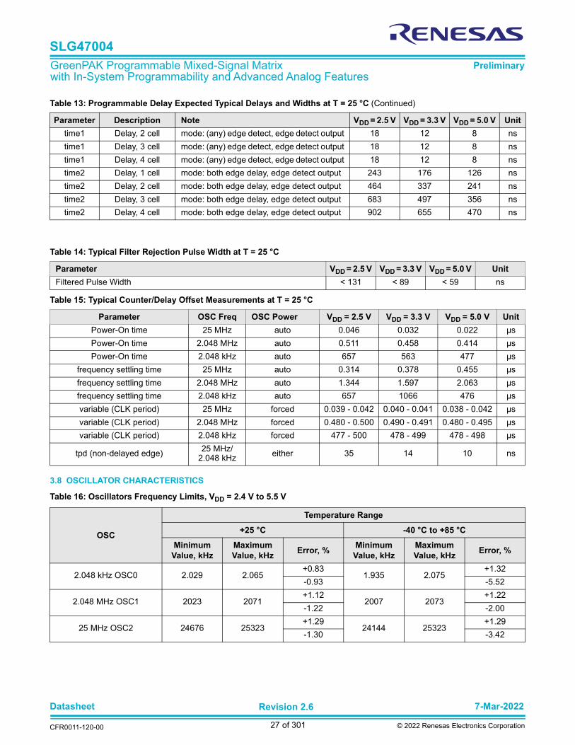
Datasheet 7-Mar-2022
CFR0011-120-00
Revision 2.6
27 of 301 © 2022 Renesas Electronics Corporation
SLG47004
GreenPAK Programmable Mixed-Signal Matrix with In-System Programmability and Advanced Analog Features
Preliminary
3.8 OSCILLATOR CHARACTERISTICS
time1 Delay, 2 cell mode: (any) edge detect, edge detect output 18 12 8 ns
time1 Delay, 3 cell mode: (any) edge detect, edge detect output 18 12 8 ns
time1 Delay, 4 cell mode: (any) edge detect, edge detect output 18 12 8 ns
time2 Delay, 1 cell mode: both edge delay, edge detect output 243 176 126 ns
time2 Delay, 2 cell mode: both edge delay, edge detect output 464 337 241 ns
time2 Delay, 3 cell mode: both edge delay, edge detect output 683 497 356 ns
time2 Delay, 4 cell mode: both edge delay, edge detect output 902 655 470 ns
Table 14: Typical Filter Rejection Pulse Width at T = 25 °C
Parameter VDD = 2.5 V VDD = 3.3 V VDD = 5.0 V Unit
Filtered Pulse Width < 131 < 89 < 59 ns
Table 15: Typical Counter/Delay Offset Measurements at T = 25 °C
Parameter OSC Freq OSC Power VDD = 2.5 V VDD = 3.3 V VDD = 5.0 V Unit
Power-On time 25 MHz auto 0.046 0.032 0.022 µs
Power-On time 2.048 MHz auto 0.511 0.458 0.414 µs
Power-On time 2.048 kHz auto 657 563 477 µs
frequency settling time 25 MHz auto 0.314 0.378 0.455 µs
frequency settling time 2.048 MHz auto 1.344 1.597 2.063 µs
frequency settling time 2.048 kHz auto 657 1066 476 µs
variable (CLK period) 25 MHz forced 0.039 - 0.042 0.040 - 0.041 0.038 - 0.042 µs
variable (CLK period) 2.048 MHz forced 0.480 - 0.500 0.490 - 0.491 0.480 - 0.495 µs
variable (CLK period) 2.048 kHz forced 477 - 500 478 - 499 478 - 498 µs
tpd (non-delayed edge) 25 MHz/2.048 kHz either 35 14 10 ns
Table 16: Oscillators Frequency Limits, VDD = 2.4 V to 5.5 V
OSC
Temperature Range
+25 °C -40 °C to +85 °C
Minimum
Value, kHz
Maximum
Value, kHzError, %
Minimum
Value, kHz
Maximum
Value, kHzError, %
2.048 kHz OSC0 2.029 2.065+0.83
1.935 2.075+1.32
-0.93 -5.52
2.048 MHz OSC1 2023 2071+1.12
2007 2073+1.22
-1.22 -2.00
25 MHz OSC2 24676 25323+1.29
24144 25323+1.29
-1.30 -3.42
Table 13: Programmable Delay Expected Typical Delays and Widths at T = 25 °C (Continued)
Parameter Description Note VDD = 2.5 V VDD = 3.3 V VDD = 5.0 V Unit

Datasheet 7-Mar-2022
CFR0011-120-00
Revision 2.6
28 of 301 © 2022 Renesas Electronics Corporation
SLG47004
GreenPAK Programmable Mixed-Signal Matrix with In-System Programmability and Advanced Analog Features
Preliminary
3.8.1 OSC Power-On Delay
3.9 ACMP CHARACTERISTICS
Table 17: Oscillators Power-On Delay at T = 25 °C, OSC Power Setting: "Auto Power-On"
Power Supply Range
(VDD), V
OSC0 2.048 kHz OSC1 2.048 MHz OSC2 25 MHz OSC2 25 MHz
Start with Delay
TypicalValue, µs
MaximumValue, µs
TypicalValue, ns
MaximumValue, ns
TypicalValue, ns
MaximumValue, ns
TypicalValue, ns
MaximumValue, ns
2.50 492 559 491 500 46 53 145 153
3.30 490 525 489 501 32 37 140 148
4.00 489 509 489 509 26 31 139 146
5.00 488 495 488 530 22 26 138 146
5.50 488 499 487 532 20 24 138 145
Table 18: ACMP Specifications at T = -40 °C to +85 °C, VDD = 2.4 V to 5.5 V Unless Otherwise Noted
Parameter Description Conditions Note Min Typ Max Unit
VACMPACMP Input Voltage Range
Positive Input 0 -- VDD V
Negative Input 0 -- VDD V
Voffset
ACMP Input Offset ACMPxL, Vhys = 0 mV, Gain = 1,Vref = 32 mV to 2048 mV
T = -40 °C to +85 °C -6.27 -- 3.67 mV
T = 25 °C -5.76 -0.98 3.39 mV
Chopper ACMP Input Offset
T = -40 °C to +85 °C -0.24 -- 0.49 mV
T = 25 °C -0.12 0.11 0.39 mV
tstart
ACMP Startup Time when BG ON
ACMP Power-On delay, Minimal required wake time for the "Wake and Sleep function", for ACMPxL
T = -40 °C to +85 °C-- 51.0 99.6 µs
ACMP Startup Time when BG OFF -- 1729 2822 µs
RsinSeries Input Resistance
Gain = 1x -- 10 -- GΩ
Gain = 0.5x -- 1.6 -- MΩ
Gain = 0.33x -- 1.6 -- MΩ
Gain = 0.25x -- 1.6 -- MΩ
PROP Propagation Delay, Response Time
ACMPxL, Vref =1.024 V, Gain = 1,Overdrive = 100 mV
Low to High -- 2.59 3.66 µs
High to Low -- 2.80 5.21 µs
ACMPxL,Vref = 32 mV to 2048 mV, Gain = 1,Overdrive = 100 mV
Low to High -- 2.83 5.16 µs
High to Low -- 2.96 7.63 µs
ACMPxL, Vref =1.024 V, Gain = 1,Overdrive = 10 mV
Low to High -- 8.18 12.57 µs
High to Low -- 9.14 18.54 µs
ACMPxL,Vref = 32 mV to 2048 mV, Gain = 1,Overdrive = 10 mV
Low to High -- 9.16 21.41 µs
High to Low -- 10.01 32.37 µs
G Gain Error
G = 1 1 1 1
G = 0.5 0.496 0.5 0.504
G = 0.33 0.331 0.330 0.336
G = 0.25 0.248 0.250 0.253

Datasheet 7-Mar-2022
CFR0011-120-00
Revision 2.6
29 of 301 © 2022 Renesas Electronics Corporation
SLG47004
GreenPAK Programmable Mixed-Signal Matrix with In-System Programmability and Advanced Analog Features
Preliminary
3.10 INTERNAL VREF CHARACTERISTICS
3.11 OUTPUT BUFFERS CHARACTERISTICS
Table 19: Internal Vref Characteristics at VDD = 2.4 V to 5.5 V
Parameter Description Conditions Note Min Typ Max Unit
Vref Accuracy and Loading
Internal Vref Accuracy atVref > 1216 mV
No loading T = 25 °C -0.30 -- 0.18 %
T = -40 °C to +85 °C -0.73 -- 0.19 %
VrefACCURACY Vref Divider AccuracyVref from (16/64) to (64/64) T = -40 °C to +85 °C -0.38 0.04 0.37 %
Vref from (1/64) to (64/64) T = -40 °C to +85 °C -1.94 0.02 1.31 %
VrefOFFSET Vref Divider OffsetVref from (16/64) to (64/64) T = -40 °C to +85 °C -5.58 0.83 7.84 mV
Vref from (1/64) to (64/64) T = -40 °C to +85 °C -5.58 0.62 7.84 mV
Table 20: HD Buffer Electrical Characteristics at T = -40 °C to +85 °C, VDD = 2.4 V to 5.5 V Unless Otherwise Noted
Parameter Description Conditions Min Typ Max Unit
Offset
VOFFSET Input Offset Voltage
VDDA = 5 V, VOUT = 0.5 V to 4 V, T = 25 °C
-- 0.25 8.0 mV
VDDA = 5 V,VOUT = 0.5 V to 4 V -- -- 9.0 mV
dVOFFSET/dt Offset Drift with Temperature VOUT = VDDA/2 -- 0.75 13.5 µV/C
Output
ΔVOUT(I) Load Regulation
VDDA = 5 V, VOUT = 2.048 V, ILOAD = 0.5 mA to 2 mA,T = 25 °C
-- 0.2 1.2 mV
VDDA = 5 V, VOUT = 2.048 V, ILOAD = 0.5 mA to 5 mA, T = 25 °C
0.4 1.9 mV
ΔVOUT(U) Line Regulation VDDA = 2.5 V to 5 V,VOUT = 2.048 V, T = 25 °C -- 0.9 5.0 mV
ISС Short Circuit Current VDDA = 2.4 V to 5.5 V -- 67.8 -- mA
Shutdown Characteristics
ton Buffer Turn-On Time RLOAD = 5 kΩ, T = 25 °C, -- -- 50 µs
toff Buffer Turn-Off Time RLOAD = 5 kΩ, T = 25 °C -- 0.071 -- µs
Table 21: Vref Output Buffer at T = -40 °C to +85 °C, VDD = 2.4 V to 5.5 V Unless Otherwise Noted
Parameter Description Conditions Note Min Typ Max Unit
ΔVOUT(I) Load Regulation
VDDA = 5 V, VOUT = 2.048 V, ILOAD = 0.5 mA to 2 mA,T = 25 °C
-- -0.99 -- 1.21 mV
VDDA = 5 V, VOUT = 2.048 V, ILOAD = 0.5 mA to 5 mA, T = 25 °C
-- -0.99 -- 1.39 mV
ΔVOUT(U) Line Regulation VDDA = 2.5 V to 5 V,VOUT = 2.048 V, T = 25 °C -- -2.97 -- 5.13 mV

Datasheet 7-Mar-2022
CFR0011-120-00
Revision 2.6
30 of 301 © 2022 Renesas Electronics Corporation
SLG47004
GreenPAK Programmable Mixed-Signal Matrix with In-System Programmability and Advanced Analog Features
Preliminary
Vref Buffer Accuracy
and Loading
Vref Output Buffer Offset
Vref < 1024 mV, VDDA = 2.4 V to 5.5V,No Loading
T = 25 °C -11.2 -- 10.0 mV
-12.2 -- 10.6 mV
Vref =1024 mV to 1600 mV,VDDA = 2.4 V to 5.5V,No Loading
T = 25 °C -6.8 -- 6.2 mV
-7.3 -- 6.9 mV
Vref >1600 mV, VDDA = 2.4 V to 5.5V,No Loading
T = 25 °C -11.1 -- 11.6 mV
-12.0 -- 12.9 mV
Vref =1024 mV to 2048 mV, VDDA = 3.3 V,No Loading
T = 25 °C -6.8 -- 5.8 mV
-7.2 -- 6.4 mV
Vref0 Buffer Output Capacitance Loading
Load Resistance = 1 MΩ -- -- 5 pF
Load Resistance = 560 kΩ -- -- 10 pF
Load Resistance =100 kΩ -- -- 40 pF
Load Resistance = 10 kΩ -- -- 80 pF
Load Resistance = 2 kΩ -- -- 120 pF
Load Resistance = 1 kΩ,Vref = 32 mV to 1024 mV -- -- 150 pF
Table 21: Vref Output Buffer at T = -40 °C to +85 °C, VDD = 2.4 V to 5.5 V Unless Otherwise Noted(Continued)
Parameter Description Conditions Note Min Typ Max Unit

Datasheet 7-Mar-2022
CFR0011-120-00
Revision 2.6
31 of 301 © 2022 Renesas Electronics Corporation
SLG47004
GreenPAK Programmable Mixed-Signal Matrix with In-System Programmability and Advanced Analog Features
Preliminary
3.12 ANALOG TEMPERATURE SENSOR CHARACTERISTICS
Table 22: TS Output vs Temperature (Output Range 1)
T, °CVDD = 2.5 V VDD = 3.3 V VDD = 5.0 V
Typical, mV Accuracy, % Typical, mV Accuracy, % Typical, mV Accuracy, %
-40 991 ±0.41 989 ±0.38 989 ±0.33
-30 968 ±0.35 967 ±0.32 966 ±0.33
-20 945 ±0.33 944 ±0.31 943 ±0.34
-10 922 ±0.37 921 ±0.35 920 ±0.38
0 899 ±0.39 898 ±0.38 897 ±0.42
10 876 ±0.41 875 ±0.39 874 ±0.43
20 853 ±0.41 852 ±0.39 851 ±0.44
30 830 ±0.45 828 ±0.44 828 ±0.48
40 806 ±0.52 805 ±0.51 804 ±0.55
50 782 ±0.56 781 ±0.55 780 ±0.60
60 758 ±0.62 756 ±0.61 756 ±0.65
70 733 ±0.70 732 ±0.69 731 ±0.73
80 709 ±0.77 707 ±0.76 707 ±0.80
85 696 ±0.81 695 ±0.80 694 ±0.84
Table 23: TS Output vs Temperature (Output Range 2)
T, °CVDD = 2.5 V VDD = 3.3 V VDD = 5.0 V
Typical, mV Accuracy, % Typical, mV Accuracy, % Typical, mV Accuracy, %
-40 1195 ±0.39 1194 ±0.34 1193 ±0.34
-30 1168 ±0.37 1166 ±0.35 1165 ±0.36
-20 1141 ±0.37 1139 ±0.35 1138 ±0.36
-10 1113 ±0.40 1111 ±0.39 1110 ±0.41
0 1085 ±0.43 1084 ±0.42 1083 ±0.44
10 1057 ±0.44 1056 ±0.43 1055 ±0.45
20 1029 ±0.45 1028 ±0.44 1027 ±0.45
30 1001 ±0.48 999 ±0.47 999 ±0.50
40 972 ±0.54 971 ±0.53 970 ±0.56
50 943 ±0.58 942 ±0.57 941 ±0.60
60 914 ±0.64 913 ±0.63 912 ±0.66
70 885 ±0.72 883 ±0.71 882 ±0.74
80 855 ±0.79 854 ±0.77 853 ±0.81
85 840 ±0.83 839 ±0.81 838 ±0.84

Datasheet 7-Mar-2022
CFR0011-120-00
Revision 2.6
32 of 301 © 2022 Renesas Electronics Corporation
SLG47004
GreenPAK Programmable Mixed-Signal Matrix with In-System Programmability and Advanced Analog Features
Preliminary
3.13 PROGRAMMABLE OPERATIONAL AMPLIFIER CHARACTERISTICS
Table 24: EC of OA, VDDA = 2.4 V to 5.5 V, VCM = VDDA/2, VOUT ≈ VDDA/2, RL = 100 kΩ to VDDA/2, CL = 50 pF, T = 25 °C
Parameter Description Conditions (Note 1) Min Typ Max Unit
Input Voltage Offset (without Customers Trimming, Included Factory Block Offset Trim)
VOFFSET Input Offset Voltage
BW = 128 kHz -- 69 487 µV
BW = 128 kHz,T = -40 °C to +85 °C -- 69 915 µV
BW = 512kHz -- 56 420 µV
BW = 512 kHz,T = -40 °C to +85 °C -- 56 1006 µV
BW = 2 MHz -- 47 311 µV
BW = 2 MHz,T = -40 °C to +85 °C -- 47 780 µV
BW = 8 MHz -- 35 243 µV
BW = 8 MHz,T = -40 °C to +85 °C -- 35 643 µV
dVOFFSET/dt Offset Drift with Temperature
VCM = VDD/2,T = -40 °C to +85 °C -- 0.6 13.0 µV/°C
VCM = GND,T = -40 °C to +85 °C -- 0.5 12.6 µV/°C
dVOFFSET/Time
Long-Term Offset Voltage Drift VCM = VDD/2 0 -- 985 µV
Trimmed Input Offset (Customer Perspective after Using Digital Rheostats with Gain = 200x) (Note 2)
VOFFSET Input Offset Voltage VCM = VDD/2 -- -- 5 µV
Input Voltage Range
VCMRInput Common-Mode Voltage Range T = -40 °C to +85 °C -0.2 -- VDD
+ 0.2 V
CMRR Common-Mode Rejection Ratio
All Op Amps,GND + 0.8 V < VCM < VDD - 0.8 V,T = -40 °C to +85 °C
73.5 102 -- dB
All Op Amps,GND < VCM< GND+ 0.8 V or VDD - 0.8 V < VCM < VDD
69.7 101 -- dB
Op Amp0 and Op Amp1,GND + 0.8 V < VCM < VDD - 0.8 V,T = -40 °C to +85 °C
73.5 103 -- dB
Op Amp0 and Op Amp1,GND < VCM< GND+ 0.8 V or VDD - 0.8 V < VCM < VDD
69.7 102 -- dB
Internal Op Amp,GND + 0.8 V < VCM < VDD - 0.8 V,T = -40 °C to +85 °C
77.6 100 -- dB
Internal Op Amp,GND < VCM< GND+ 0.8 V or VDD - 0.8 V < VCM < VDD
69.7 100 -- dB
PSRR Power Supply Rejection Ratio
VCM = VDD/2,T = -40 °C to +85 °C 80 101 -- dB
VCM = GND,T = -40 °C to +85 °C 83 102 -- dB

Datasheet 7-Mar-2022
CFR0011-120-00
Revision 2.6
33 of 301 © 2022 Renesas Electronics Corporation
SLG47004
GreenPAK Programmable Mixed-Signal Matrix with In-System Programmability and Advanced Analog Features
Preliminary
CSChannel Separation VDD = 5 V, f = 10 Hz -- 119 -- dB
VDD = 5 V, f = 1 kHz -- 112 -- dB
Input Current and Impedance
IB Input Bias Current-- 1.9 ±9 pA
T = -40 °C to +85 °C -- 1.9 ±258 pA
IOFFSET Input Offset Current-- -- 3.2 pA
T = +85 °C -- 210 pA
RCMCommon-Mode Input Resistance -- 3*1012 -- Ω
RDIFFDifferential Input Resistance -- 1013 -- Ω
CCMInput Capacitance Common-Mode -- 5 7 pF
CDIFFInput Capacitance Differential -- 1.98 2.27 pF
Open-Loop Gain
AOL DC Open Loop Gain
RLOAD = 1 MΩ,GND + 0.1 V < VOUT < VDD - 0.1 V,T = -40 °C to +85 °C
103.3 125 -- dB
RLOAD = 50 kΩ,GND + 0.5 V < VOUT < VDD - 0.5 VT = -40 °C to +85 °C
103.4 125 -- dB
Output
VOH
Maximum Voltage Swing
RLOAD = 50 kΩ,T = -40 °C to +85 °C VDD - 5.73 -- -- mV
BW = 8.192 MHz,RLOAD = 600 Ω,T = -40 °C to +85 °C
VDD - 135 -- -- mV
VOL
RLOAD = 50 kΩ,T = -40 °C to +85 °C -- -- GND +
3.122 mV
BW = 8.192 MHz,RLOAD = 600 Ω,T = -40 °C to +85 °C
-- -- GND + 101 mV
VOSRLinear Output Swing Range
VOVR from RailRLOAD = 1 MΩ
GND + 100 -- VDD - 100 mV
Table 24: EC of OA, VDDA = 2.4 V to 5.5 V, VCM = VDDA/2, VOUT ≈ VDDA/2, RL = 100 kΩ to VDDA/2, CL = 50 pF, T = 25 °C
Parameter Description Conditions (Note 1) Min Typ Max Unit

Datasheet 7-Mar-2022
CFR0011-120-00
Revision 2.6
34 of 301 © 2022 Renesas Electronics Corporation
SLG47004
GreenPAK Programmable Mixed-Signal Matrix with In-System Programmability and Advanced Analog Features
Preliminary
ISС Short Circuit Current
ISC to GND
BW = 128 kHz,T = -40 °C to +85 °C -- 10.8 -- mA
BW = 512 kHz,T = -40 °C to +85 °C -- 14.4 -- mA
BW = 2.048 MHz,T = -40 °C to +85 °C -- 22.5 -- mA
BW = 8.192 MHz,T = -40 °C to +85 °C -- 52.0 -- mA
ISC to VDD
BW = 128 kHz,T = -40 °C to +85 °C 20.6 -- mA
BW = 512 kHz,T = -40 °C to +85 °C 27.0 -- mA
BW = 2.048 MHz,T = -40 °C to +85 °C 41.1 -- mA
BW = 8.192 MHz,T = -40 °C to +85 °C 92.1 -- mA
CLOAD Capacitive Load DriveSee Section 10.3
(Small Signal Overshoot vs. Capacitive Load plots)
Power Supply
VDD Supply Voltage Guaranteed by PSRR Test 2.4 -- 5.5 V
IQ(including
charge pump current
consumption)
Quiescent Current per Amplifier, BW = 128 kHz
T = 25 °C,VDDA = 2.5 V to 5.5 V -- 33.3 47 µA
T = -40 °C to +85 °C,VDDA = 2.5 V to 5.5 V -- 34.1 59 µA
Quiescent Current per Amplifier, BW = 512 kHz
T = 25 °C,VDDA = 2.5 V to 5.5 V -- 89.8 101 µA
T = -40 °C to +85 °C,VDDA = 2.5 V to 5.5 V -- 91.1 124 µA
Quiescent Current per Amplifier,BW = 2.048 MHz
T = 25 °C,VDDA = 2.5 V to 5.5 V -- 238.7 255 µA
T = -40 °C to +85 °C,VDDA = 2.5 V to 5.5 V -- 238.9 274 µA
Quiescent Current per Amplifier,BW = 8.192 MHz
T = 25 °C,VDDA = 2.5 V to 5.5 V -- 611.5 652 µA
T = -40 °C to +85 °C,VDDA = 2.5 V to 5.5 V -- 611.6 701 µA
IQ(including
charge pump current
consumption)
Full Shutdown T = 25 °C -- 105.8 -- nA
Partial Shutdown (Note 3), BW = 128 kHz
T = 25 °C -- 7.3 -- µA
Partial Shutdown(Note 3),BW = 8.192 MHz
T = 25 °C -- 21.3 -- µA
Frequency Response
Table 24: EC of OA, VDDA = 2.4 V to 5.5 V, VCM = VDDA/2, VOUT ≈ VDDA/2, RL = 100 kΩ to VDDA/2, CL = 50 pF, T = 25 °C
Parameter Description Conditions (Note 1) Min Typ Max Unit

Datasheet 7-Mar-2022
CFR0011-120-00
Revision 2.6
35 of 301 © 2022 Renesas Electronics Corporation
SLG47004
GreenPAK Programmable Mixed-Signal Matrix with In-System Programmability and Advanced Analog Features
Preliminary
GBWGain Bandwidth Product
RLOAD = 10 kΩ,CLOAD = 20 pF,G = +1 V/V,T = -40 °C to+85 °C
BW = 128 kHz -- 124 -- kHz
BW = 512 kHz -- 542 -- kHz
BW = 2.048 MHz -- 2569 -- kHz
BW = 8.192 MHz -- 9594 -- kHz
PM Phase Margin
G = +1 V/V,BW = 128 kHz → 8.192 MHz;RLOAD = 10 kΩ, CLOAD = 20 pF,T = -40 °C to +85 °C
43 71 -- degree
SR Slew RateRLOAD = 50 kΩ, CLOAD = 85 pF
BW = 128 kHz,T = -40 °C to +85 °C -- 0.09 -- V/µs
BW = 512 kHz,T = -40 °C to +85 °C -- 0.38 -- V/µs
BW = 2.048 MHz,T = -40 °C to +85 °C -- 1.85 -- V/µs
BW = 8.192 MHz,T = -40 °C to +85 °C -- 6.48 -- V/µs
tOROverload Recovery Time
T = -40 °C to +85 °CRLOAD = 50 kΩ -- 12.68 -- µs
Noise
THD Total Harmonic Distortion
AV = 1, RLOAD = 50 kΩ,VOUT(PP) = VDD/2
f = 1 kHz,BW = 128 kHz -- 0.171 -- %
f = 1 kHz,BW = 512 kHz -- 0.073 -- %
f = 1 kHz,BW = 2.048 MHz -- 0.033 -- %
f = 1 kHz, BW = 8.192 MHz -- 0.02 -- %
en Input Voltage Noise f = 0.1 to 10 Hz -- 2.54 -- µVpp
VnInput Voltage Noise Density f = 1 kHz
BW = 128 kHz -- 92 --nV/
BW = 512 kHz -- 86 --
BW = 2.048 MHz -- 74 --
BW = 8.192 MHz -- 51 --
In Input Current Noise Density f = 1 kHz -- 1 --
fA/
Shutdown Characteristics
tonAmplifier Turn-On Time
BW = 8.192 MHz,T = -40 °C to +85 °C
VCM = VDDA/2,RL = 50 kΩ -- 2.143 6.095 µs
VDDA > VCM > (VDDA - 1.3) -- 2.166 6.070 µs
BW = 128 kHz,T = -40 °C to +85 °C
VCM = VDDA/2,RL = 50 kΩ -- 25.177 43.158 µs
VDDA > VCM > (VDDA - 1.3) -- 34.769 70.602 µs
toffAmplifier Turn-Off Time -- -- 0.653 1.015 µs
Table 24: EC of OA, VDDA = 2.4 V to 5.5 V, VCM = VDDA/2, VOUT ≈ VDDA/2, RL = 100 kΩ to VDDA/2, CL = 50 pF, T = 25 °C
Parameter Description Conditions (Note 1) Min Typ Max Unit
Hz
Hz

Datasheet 7-Mar-2022
CFR0011-120-00
Revision 2.6
36 of 301 © 2022 Renesas Electronics Corporation
SLG47004
GreenPAK Programmable Mixed-Signal Matrix with In-System Programmability and Advanced Analog Features
Preliminary
3.14 100K DIGITAL RHEOSTAT CHARACTERISTICS
Comparator Mode
tPHLPropagation Delay Output High to Low Vref = 2.048 mV,
Overdrive =100 mV,Charge Pump is always On
BW = 128 kHz -- 23.6 39.4 µs
BW = 512 kHz -- 10.8 17.9 µs
BW = 2.048 MHz -- 6.8 11.5 µs
BW = 8.192 MHz -- 5.6 10.0 µs
tPLHPropagation Delay Output Low to High
BW = 128 kHz -- 24.6 40.1 µs
BW = 512 kHz -- 10.6 17.2 µs
BW = 2.048 MHz -- 6.5 10.8 µs
BW = 8.192 MHz -- 5.4 9.0 µs
Note 1 AGND = GND, unless otherwise notedNote 2 Equivalent offset voltage of the amplifier after user’s trim using digital rheostat. Gain of the amplifier is G=200 and the zero output voltage level Vzero = VDD/2 (See Section 10.2.1)Note 3 Op amps analog supporting blocks are always turned on.
Table 25: 100K Digital Rheostat EC at VA=VDD, VB=GND, T=-40°C to +85°C, VDD=2.4V to 5.5V Unless Otherwise Noted
Parameter Description Conditions Min Typ Max Unit
VDRRheostat Pin Voltage Range
Voltage between any (A or B) pins and AGND AGND -- VDDA V
RDRDigital Rheostat Resistance
Full resistance with all switches open (Note 1)
94.426 101.582 113.741 kΩ
RDR_MINMinimal Rheostat Resistance Code = 0x00 43.679 -- 84.779 Ω
RMATCHMismatch between rheostats Code = 0x3FF, T = 25 °C -- 0.084 -- %
Number of taps 1024
BWDTDR Digital Rheostat Bandwidth
Frequency applied on one side of resistor chain and -3 dB frequency measured at the other side with full 100 KΩ, assume no additional load
-- 50 -- kHz
Vcharge+
Positive charge pumpvoltage (for the CMOS N-chMOSFET)
-- ±5 -- V
RS Step ResistanceVDD = (2.4 V; 3.3 V; 5.5 V)VDDA = (1 V; -1 V)T= (-40 °C; 25 °C; 85 °C)
-- 99.236 -- Ω
IDR_MAXMax current through Rheostat T = 25 °C+ -- -- 2 mA
ESW_N Resistor Noise Voltage RAB = 25 kΩ, f = 1 kHz -- 30 -- nV/√Hz
fChACMPChopper Comparator Switching Frequency -- -- 30 kHz
VCh_offset
Chopper comparator offset when Auto-Trim process is active
-- 100 300 µV
Table 24: EC of OA, VDDA = 2.4 V to 5.5 V, VCM = VDDA/2, VOUT ≈ VDDA/2, RL = 100 kΩ to VDDA/2, CL = 50 pF, T = 25 °C
Parameter Description Conditions (Note 1) Min Typ Max Unit

Datasheet 7-Mar-2022
CFR0011-120-00
Revision 2.6
37 of 301 © 2022 Renesas Electronics Corporation
SLG47004
GreenPAK Programmable Mixed-Signal Matrix with In-System Programmability and Advanced Analog Features
Preliminary
3.15 ANALOG SWITCHES CHARACTERISTICS
fDR_CLK
Counter Frequency independent from the Rheostat
The counter frequency is determined by user selection 0 -- 25 MHz
fDR_SWCHRheostat Switch Speed (Note 2)
VA = 5 V, VB = 0 V, ±1 LSB error band, Auto-Trim or Fast mode
-- -- 100 kHz
VA = 5 V, VB = 0 V, ±1 LSB error band, regular mode -- -- 1 kHz
Tsettle
Fast mode, I2C code change from 0 to 1023 -- -- 50 µs
Fast mode, Rheostat 1 bit code change -- -- 10 µs
СDR
Maximum Capacitance of A, B pins Measured to AGND
All switches are ON,f = 200 kHz -- 33.152 -- pF
ILKG Leakage Current Including active charge pump current consumption -- -- 1000 nA
ErrorZScale Zero-Scale Error Code = 0x00 -- -- 0.776 LSB
INL IntegralNon-linearity -- -- ±2 LSB
DNL DifferentialNon-linearity -- -- ±1 LSB
BWDTCAPBandwidth -3 dB(Load = 30 pF)
RLOAD <12.5 kΩ -- 240 -- kHz
RLOAD = 12.5 kΩ to 25 kΩ -- 120 -- kHz
RLOAD = 25 kΩ to 50 kΩ -- 60 -- kHz
RLOAD = 50 kΩ to 100 kΩ -- 30 -- kHz
αR(T) Resistance TemperatureCoefficient VAB = const, -119.69 0 163.84 ppm/
°C
Note 1 User can calculate actual Digital Rheostat value using calibration data from NVM (see Section 12.2).Note 2 Includes internal timing. External circuit should be counted separately.
Table 26: Analog Switch0/Voltage Regulator EС at T = -40 °C to +85 °C, VDD = 2.4 V to 5.5 V Unless Otherwise Noted
Parameter Description Conditions Min Typ Max Unit
VASMaximum Voltage At Pins Voltage between any Analog
Switch pin to AGND 0 -- VDD + 0.3 V
fMAXMaximum Switching Frequency
Pull Up 2.5 -- -- MHz
Pull Up, VDD = 2.4 V 3.9 -- -- MHz
Pull Down 363 -- -- kHz
Pull Down, VDD = 2.4 V 363 -- -- kHz
RON ON Resistance
VDD = 3.3 V,VIN < 1.2 V,N-ch FET, T = 25 °C
-- 30 53 Ω
VDD = 3.3 V,VIN > VDD - 1.2,P-ch FET, T = 25 °C
-- 2 3 Ω
Table 25: 100K Digital Rheostat EC at VA=VDD, VB=GND, T=-40°C to +85°C, VDD=2.4V to 5.5V Unless Otherwise Noted
Parameter Description Conditions Min Typ Max Unit

Datasheet 7-Mar-2022
CFR0011-120-00
Revision 2.6
38 of 301 © 2022 Renesas Electronics Corporation
SLG47004
GreenPAK Programmable Mixed-Signal Matrix with In-System Programmability and Advanced Analog Features
Preliminary
IPWROFFOFF Leakage Current Switch OFF; from IN to OUT
VA = VDD or VB = VDD-- -- 17 nA
ISW_MAXMaximum ON-state Switch Current
VA = VDD, load connected to ground, VAB= 0.4 V -- -- 300 mA
ISW_PULSEMaximum Pulse Current Through Switch
Pulse duration = 1 ms,Duty cycle < 5 % -- -- 500 mA
Table 27: Analog Switch1/Current Sink EС at T = -40 °C to +85 °C, VDD = 2.4 V to 5.5 V Unless Otherwise Noted
Parameter Description Conditions Min Typ Max Unit
VASMaximum Voltage At Pins Voltage between any Analog
Switch pin to AGND 0 -- VDD + 0.3 V
fMAXMaximum Switching Frequency
Pull Up 1.6 -- -- MHz
Pull Up, VDD = 2.4 V 1.6 -- -- MHz
Pull Down 5 -- -- MHz
Pull Down, VDD = 2.4 V 5 -- -- MHz
RON ON Resistance
VDD = 3.3 V,VIN < 1.2 V,N-ch FET, T = 25 °C
-- 0.8 1.5 Ω
VDD = 3.3 V,VIN > VDD - 1.2,P-ch FET, T = 25 °C
-- 53.4 204 Ω
IPWROFF OFF Leakage Current Switch OFF; from IN to OUT,VA = VDD or VB = VDD
-- -- 34 nA
ISW_MAXMaximum ON-state Switch Current
VA = VDD, load connected to ground, VAB= 0.4 V -- -- 300 mA
ISW_PULSEMaximum Pulse Current Through Switch
Pulse duration = 1 ms,Duty cycle < 5 % -- -- 500 mA
Table 26: Analog Switch0/Voltage Regulator EС at T = -40 °C to +85 °C, VDD = 2.4 V to 5.5 V Unless Otherwise Noted
Parameter Description Conditions Min Typ Max Unit

Datasheet 7-Mar-2022
CFR0011-120-00
Revision 2.6
39 of 301 © 2022 Renesas Electronics Corporation
SLG47004
GreenPAK Programmable Mixed-Signal Matrix with In-System Programmability and Advanced Analog Features
Preliminary
4 User Programmability
The SLG47004 is a user programmable device with Multiple-Time-Programmable (MTP) memory elements that are able toconfigure the connection matrix and macrocells. A programming development kit allows the user the ability to create initialdevices. Once the design is finalized, the programming code (.aap file) is forwarded to Renesas Electronics Corporation tointegrate into a production process.
Figure 2: Steps to Create a Custom GreenPAK Device
Product
Definition
E-mail Product Idea, Definition, Drawing,
or Schematic to [email protected]
Renesas Electronics Applications
Engineers review design specifications
with customer
Samples, Design, and Characterization
Report are sent to customer
Customer verifies GreenPAK design
Customer creates their own design in
GreenPAK Designer
Customer verifies GreenPAK in system
design
Custom GreenPAK part enters production
GreenPAK Design
approved
GreenPAK Design
approved in system test
GreenPAK Design
approved

Datasheet 7-Mar-2022
CFR0011-120-00
Revision 2.6
40 of 301 © 2022 Renesas Electronics Corporation
SLG47004
GreenPAK Programmable Mixed-Signal Matrix with In-System Programmability and Advanced Analog Features
Preliminary
5 IO Pins
The SLG47004 has a total of 7 GPIO Pins which can function as either a user-defined Input or Output, as well as serve as aspecial function (such as outputting the voltage reference) and 1 GPI Pin.
5.1 GPIO PINS
IO0, IO1, IO2, IO3, IO4, IO5, and IO6 serve as General Purpose IO Pins.
5.2 GPI PINS
I0 serves as General Purpose Input Pin. It is strongly recommended to connect I0 (Pin21) to the ground if it is not used in theproject.
5.3 PULL-UP/DOWN RESISTORS
All IO Pins have the option of user-selectable resistors that can be connected to the pin structure. The selectable values on theseresistors are 10 kΩ, 100 kΩ, and 1 MΩ. The internal resistors can be configured as either Pull-up or Pull-downs.
5.4 FAST PULL-UP/DOWN DURING POWER-UP
During power-up, IO Pull-up/down resistance will switch to 2.6 kΩ initially and then it will switch to normal setting value. Thisfunction is enabled by register [1207].

Datasheet 7-Mar-2022
CFR0011-120-00
Revision 2.6
41 of 301 © 2022 Renesas Electronics Corporation
SLG47004
GreenPAK Programmable Mixed-Signal Matrix with In-System Programmability and Advanced Analog Features
Preliminary
5.5 I2C MODE IO STRUCTURE
5.5.1 I2C Mode Structure (for SCL and SDA)
Figure 3: IO with I2C Mode IO Structure Diagram
WOSMT_EN
Digital IN
LV_EN
Non-SchmittTrigger Input
VDD
VDD
Low Voltage
Input 1
PAD
I2C SDA (SCL) Signal
Input Mode [1:0]
00: Digital In without Schmitt Trigger, wosmt_en = 101: Digital In with Schmitt Trigger, smt_en = 110: Low Voltage Digital In mode 1, lv_en = 1
11: Reserved
not available for direct user control
SMT_EN
Schmitt
Trigger Input
VDD

Datasheet 7-Mar-2022
CFR0011-120-00
Revision 2.6
42 of 301 © 2022 Renesas Electronics Corporation
SLG47004
GreenPAK Programmable Mixed-Signal Matrix with In-System Programmability and Advanced Analog Features
Preliminary
5.6 MATRIX OE IO STRUCTURE
Figure 4: Matrix OE IO Structure Diagram
Digital OUT
OE
PP1x_EN
Digital OUT
OE
PP2x_EN
Digital OUT
OE
OD1x_EN
Digital OUT
OE
OD2x_EN
172 Ω(Note 2)
LV_EN
SMT_EN
WOSMT_EN
Digital IN
s0
s1
s2
s3
Analog IO
900 kΩ 90 kΩ 10 kΩ
Floating
s1
s0
Pull-up_EN
Res_sel [1:0]
00: Floating
01: 10 kΩ10: 100 kΩ11: 1 MΩ
Non-Schmitt
Trigger Input
Schmitt
Trigger Input
Low Voltage
Input
Input Mode registers [1153:1152]
00: Digital In without Schmitt Trigger, wosmt_en = 1
01: Digital In with Schmitt Trigger, smt_en = 1
10: Low Voltage Digital In mode, lv_en = 111: analog IO mode
Output Mode [1:0]
00: Push-Pull 1x mode, pp1x_en = 1
01: Push-Pull 2x mode, pp2x_en = 1, pp1x_en = 1
10: NMOS 1x Open-Drain mode, od1x_en = 1
11: NMOS 2x Open-Drain mode, od2x_en = 1, od1x_en = 1
Note 1: Digital Out and OE are Matrix Output, Digital In is Matrix Input.
Note 2: Can be varied over PVT, for reference only.
VDD
VDD
VDD
VDD
PAD

Datasheet 7-Mar-2022
CFR0011-120-00
Revision 2.6
43 of 301 © 2022 Renesas Electronics Corporation
SLG47004
GreenPAK Programmable Mixed-Signal Matrix with In-System Programmability and Advanced Analog Features
Preliminary
5.7 GPI STRUCTURE
5.7.1 GPI Structure (for I0)
Figure 5: IO0 GPI Structure Diagram
LV_EN
SMT_EN
WOSMT_EN
OE
Digital IN
s0
s1
s2
s3
900 kΩ 90 kΩ 10 kΩ
Floating
s1
s0
Pull-up_EN
Res_sel [1:0]
00: Floating
01: 10 kΩ10: 100 kΩ11: 1 MΩ
Non-Schmitt
Trigger Input
Schmitt
Trigger Input
Low VoltageInput
VDD
Input Mode [1:0]
00: Digital In without Schmitt Trigger, wosmt_en = 1, OE=0
01: Digital In with Schmitt Trigger, smt_en = 1, OE = 0
10: Low Voltage Digital In mode, lv_en = 1, OE = 0
11: Reserved
Note 1: OE cannot be selected by user.
Note 2: OE is Matrix output, Digital In is Matrix input.
OE
OE
PAD

Datasheet 7-Mar-2022
CFR0011-120-00
Revision 2.6
44 of 301 © 2022 Renesas Electronics Corporation
SLG47004
GreenPAK Programmable Mixed-Signal Matrix with In-System Programmability and Advanced Analog Features
Preliminary
5.8 IO PINS TYPICAL PERFORMANCE
Figure 6: Typical High Level Output Current vs. High Level Output Voltage at T = 25 °C
Figure 7: Typical Low Level Output Current vs. Low Level Output Voltage, 1x Drive at T = 25 °C, Full Range
0
10
20
30
40
50
60
1.251.501.752.002.252.502.753.003.253.503.754.004.254.504.755.00
I OH
(mA
)
VOH (V)
Push-Pull 2x @ VDD = 5 V
Push-Pull 1x @ VDD = 5 V
Push-Pull 2x @ VDD = 3.3 V
Push-Pull 1x @ VDD = 3.3 V
Push-Pull 2x @ VDD = 2.5 V
Push-Pull 1x @ VDD = 2.5 V
0
10
20
30
40
50
60
70
80
0 0.25 0.5 0.75 1 1.25 1.5 1.75 2 2.25 2.5
I OL
(mA
)
VOL (V)
Open Drain 1x @ VDD = 5 V
Open Drain 1x @ VDD = 3.3 V
Open Drain 1x @ VDD = 2.5 V
Push-Pull 1x @ VDD = 5 V
Push-Pull 1x @ VDD = 3.3 V
Push-Pull 1x @ VDD = 2.5 V

Datasheet 7-Mar-2022
CFR0011-120-00
Revision 2.6
45 of 301 © 2022 Renesas Electronics Corporation
SLG47004
GreenPAK Programmable Mixed-Signal Matrix with In-System Programmability and Advanced Analog Features
Preliminary
Figure 8: Typical Low Level Output Current vs. Low Level Output Voltage, 1x Drive at T = 25 °C
Figure 9: Typical Low Level Output Current vs. Low Level Output Voltage, 2x Drive at T = 25 °C, Full Range
0
5
10
15
20
25
30
0 0.1 0.2 0.3 0.4 0.5
I OL
(mA
)
VOL (V)
Open Drain 1x @ VDD = 5 V
Open Drain 1x @ VDD = 3.3 V
Open Drain 1x @ VDD = 2.5 V
Push-Pull 1x @ VDD = 5 V
Push-Pull 1x @ VDD = 3.3 V
Push-Pull 1x @ VDD = 2.5 V
0
10
20
30
40
50
60
70
80
90
100
110
120
130
140
0 0.25 0.5 0.75 1 1.25 1.5 1.75 2 2.25 2.5
I OL
(mA
)
VOL (V)
Open Drain 2x @ VDD = 5 V
Open Drain 2x @ VDD = 3.3 V
Open Drain 2x @ VDD = 2.5 V
Push-Pull 2x @ VDD = 5 V
Push-Pull 2x @ VDD = 3.3 V
Push-Pull 2x @ VDD = 2.5 V

Datasheet 7-Mar-2022
CFR0011-120-00
Revision 2.6
46 of 301 © 2022 Renesas Electronics Corporation
SLG47004
GreenPAK Programmable Mixed-Signal Matrix with In-System Programmability and Advanced Analog Features
Preliminary
Figure 10: Typical Low Level Output Current vs. Low Level Output Voltage, 2x Drive at T = 25 °C
0
5
10
15
20
25
30
35
40
45
50
0 0.1 0.2 0.3 0.4 0.5
I OL
(mA
)
VOL (V)
Open Drain 2x @ VDD = 5 V
Open Drain 2x @ VDD = 3.3 V
Open Drain 2x @ VDD = 2.5 V
Push-Pull 2x @ VDD = 5 V
Push-Pull 2x @ VDD = 3.3 V
Push-Pull 2x @ VDD = 2.5 V

Datasheet 7-Mar-2022
CFR0011-120-00
Revision 2.6
47 of 301 © 2022 Renesas Electronics Corporation
SLG47004
GreenPAK Programmable Mixed-Signal Matrix with In-System Programmability and Advanced Analog Features
Preliminary
6 Connection Matrix
The Connection Matrix in the SLG47004 is used to create an internal routing for internal functional macrocells of the deviceonce it is programmed. The output of each functional macrocell within the SLG47004 has a specific digital bit code assigned toit, that is either set to active "High" or inactive "Low", based on the design that is created. Once the 2048 register bits within theSLG47004 are programmed, a fully custom circuit will be created.
The Connection Matrix has 64 inputs and 99 outputs. Each of the 64 inputs to the Connection Matrix is hard-wired to the digitaloutput of a particular source macrocell, including IOs, LUTs, analog comparators, other digital resources, such as VDD and GND.The input to a digital macrocell uses a 6-bit register to select one of these 64 input lines.
For a complete list of the SLG47004’s register table, see Section 21.
Figure 11: Connection Matrix
Figure 12: Connection Matrix Example
GND 0
LUT2_0/DFF0 output 1
LUT2_1/DFF1 output 2
LUT2_2/DFF2 output 3
Matrix Input Signal Functions
N
VDD 62
VDD 63
N
Function
Registers
99
OP Vref ENABLE
registers [599:594]
0
Matrix OUT: IN0 of LUT2_0 or Clock
Input of DFF0
registers [5:0]
1
Matrix OUT: IN1 of LUT2_0 or DataInput of DFF0
registers [11:6]
2
Matrix Out: IN0 of LUT2_1 or Clock
Input of DFF1
registers [17:12]
Matrix Inputs
Matrix Outputs
IO12
IO13
IO14
Connection Matrix
LUT
IO13
IO12
LUTIO14
Function

Datasheet 7-Mar-2022
CFR0011-120-00
Revision 2.6
48 of 301 © 2022 Renesas Electronics Corporation
SLG47004
GreenPAK Programmable Mixed-Signal Matrix with In-System Programmability and Advanced Analog Features
Preliminary
6.1 MATRIX INPUT TABLE
Table 28: Matrix Input Table
Matrix Input
NumberMatrix Input Signal Function
Matrix Decode
5 4 3 2 1 0
0 GND 0 0 0 0 0 0
1 LUT2_0/DFF0 output 0 0 0 0 0 1
2 LUT2_1/DFF1 output 0 0 0 0 1 0
3 LUT2_2/DFF2 output 0 0 0 0 1 1
4 LUT2_3/PGen output 0 0 0 1 0 0
5 LUT3_0/DFF3 output 0 0 0 1 0 1
6 LUT3_1/DFF4 output 0 0 0 1 1 0
7 LUT3_2/DFF5 output 0 0 0 1 1 1
8 LUT3_3/DFF6 output 0 0 1 0 0 0
9 LUT3_4/DFF7 output 0 0 1 0 0 1
10 LUT3_5/DFF8 output 0 0 1 0 1 0
11 LUT3_6/DFF9 output 0 0 1 0 1 1
12 CNT_DLY0 output 0 0 1 1 0 0
13 MLT0_LUT4_1/DFF17_OUT 0 0 1 1 0 1
14 CNT_DLY1 output 0 0 1 1 1 0
15 MLT1_LUT3_7/DFF11_OUT 0 0 1 1 1 1
16 CNT_DLY2 output 0 1 0 0 0 0
17 MLT2_LUT3_8/DFF12_OUT 0 1 0 0 0 1
18 CNT_DLY3 output 0 1 0 0 1 0
19 MLT3_LUT3_9/DFF13_OUT 0 1 0 0 1 1
20 CNT_DLY4 output 0 1 0 1 0 0
21 MLT4_LUT3_10/DFF14_OUT 0 1 0 1 0 1
22 CNT_DLY5 output 0 1 0 1 1 0
23 MLT5_LUT3_11/DFF15_OUT 0 1 0 1 1 1
24 CNT_DLY6 output 0 1 1 0 0 0
25 MLT6_LUT3_12/DFF16_OUT 0 1 1 0 0 1
26 LUT3_13/Pipe Delay/RippleCNT_out0 0 1 1 0 1 0
27 Pipe Delay/RippleCNT_out1 0 1 1 0 1 1
28 Pipe Delay/RippleCNT_out2 0 1 1 1 0 0
29 LUT4_0/DFF10 output 0 1 1 1 0 1
30 Programmable Delay Edge Detect Output 0 1 1 1 1 0
31 Edge Detect Filter Output 0 1 1 1 1 1
32 I2C_virtual_0 Input 1 0 0 0 0 0
33 I2C_virtual_1 Input 1 0 0 0 0 1
34 I2C_virtual_2 Input 1 0 0 0 1 0
35 I2C_virtual_3 Input 1 0 0 0 1 1
36 I2C_virtual_4 Input 1 0 0 1 0 0
37 I2C_virtual_5 Input 1 0 0 1 0 1

Datasheet 7-Mar-2022
CFR0011-120-00
Revision 2.6
49 of 301 © 2022 Renesas Electronics Corporation
SLG47004
GreenPAK Programmable Mixed-Signal Matrix with In-System Programmability and Advanced Analog Features
Preliminary
6.2 MATRIX OUTPUT TABLE
38 I2C_virtual_6 Input 1 0 0 1 1 0
39 I2C_virtual_7 Input 1 0 0 1 1 1
40 RH0 Idle/Active 1 0 1 0 0 0
41 RH1 Idle/Active 1 0 1 0 0 1
42 Output of Op Amp0 in ACMP mode 1 0 1 0 1 0
43 Output of Op Amp1 in ACMP mode 1 0 1 0 1 1
44 IO0 Digital Input 1 0 1 1 0 0
45 IO1 Digital Input 1 0 1 1 0 1
46 IO2 Digital Input 1 0 1 1 1 0
47 IO3 Digital Input 1 0 1 1 1 1
48 IO4 Digital Input 1 1 0 0 0 0
49 IO5 Digital Input 1 1 0 0 0 1
50 IO6 Digital Input 1 1 0 0 1 0
51 I0 Digital Input 1 1 0 0 1 1
52 Oscillator0 output 0 1 1 0 1 0 0
53 Oscillator1 output 0 1 1 0 1 0 1
54 Oscillator2 output 1 1 0 1 1 0
55 Chopper ACMP Out 1 1 0 1 1 1
56 ACMP0 Output (low speed) 1 1 1 0 0 0
57 ACMP1 Output (low speed) 1 1 1 0 0 1
58 Oscillator0 output 1 1 1 1 0 1 0
59 Oscillator1 output 1 1 1 1 0 1 1
60 POR OUT 1 1 1 1 0 0
61 VDD 1 1 1 1 0 1
62 VDD 1 1 1 1 1 0
63 VDD 1 1 1 1 1 1
Table 29: Matrix Output Table
Register Bit
AddressMatrix Output Signal Function
Matrix Output
Number
[5:0] IN0 of LUT2_0 or Clock Input of DFF0 0
[11:6] IN1 of LUT2_0 or Data Input of DFF0 1
[17:12] IN0 of LUT2_1 or Clock Input of DFF1 2
[23:18] IN1 of LUT2_1 or Data Input of DFF1 3
[29:24] IN0 of LUT2_2 or Clock Input of DFF2 4
[35:30] IN1 of LUT2_2 or Data Input of DFF2 5
[41:36] IN0 of LUT2_3 or Clock Input of PGen 6
[47:42] IN1 of LUT2_3 or nRST of PGen 7
[53:48] IN0 of LUT3_0 or CLK Input of DFF3 8
Table 28: Matrix Input Table(Continued)
Matrix Input
NumberMatrix Input Signal Function
Matrix Decode
5 4 3 2 1 0

Datasheet 7-Mar-2022
CFR0011-120-00
Revision 2.6
50 of 301 © 2022 Renesas Electronics Corporation
SLG47004
GreenPAK Programmable Mixed-Signal Matrix with In-System Programmability and Advanced Analog Features
Preliminary
[59:54] IN1 of LUT3_0 or Data of DFF3 9
[65:60] IN2 of LUT3_0 or nRST (nSET) of DFF3 10
[71:66] IN0 of LUT3_1 or CLK Input of DFF4 11
[77:72] IN1 of LUT3_1 or Data of DFF4 12
[83:78] IN2 of LUT3_1 or nRST (nSET) of DFF4 13
[89:84] IN0 of LUT3_2 or CLK Input of DFF5 14
[95:90] IN1 of LUT3_2 or Data of DFF5 15
[101:96] IN2 of LUT3_2 or nRST(nSET) of DFF5 16
[107:102] IN0 of LUT3_3 or CLK Input of DFF6 17
[113:108] IN1 of LUT3_3 or Data of DFF6 18
[119:114] IN2 of LUT3_3 or nRST (nSET) of DFF6 19
[125:120] IN0 of LUT3_4 or CLK Input of DFF7 20
[131:126] IN1 of LUT3_4 or Data of DFF7 21
[137:132] IN2 of LUT3_4 or nRST (nSET) of DFF7 22
[143:138] IN0 of LUT3_5 or CLK Input of DFF8 23
[149:144] IN1 of LUT3_5 or Data of DFF8 24
[155:150] IN2 of LUT3_5 or nRST (nSET) of DFF8 25
[161:156] IN0 of LUT3_6 or CLK Input of DFF9 26
[167:162] IN1 of LUT3_6 or CLK Input of DFF9 27
[173:168] IN2 of LUT3_6 or nRST (nSET) of DFF9 28
[179:174] IN0 of LUT3_7 or CLK Input of DFF11Delay1 Input (or Counter1 nRST Input)
29
[185:180] IN1 of LUT3_7 or nRST (nSET) of DFF11Delay1 Input (or Counter1 nRST Input)
30
[191:186] IN2 of LUT3_7 or Data of DFF11Delay1 Input (or Counter1 nRST Input)
31
[197:192] IN0 of LUT3_8 or CLK Input of DFF12Delay2 Input (or Counter2 nRST Input)
32
[203:198] IN1 of LUT3_8 or nRST (nSET) of DFF12Delay2 Input (or Counter2 nRST Input)
33
[209:204] IN2 of LUT3_8 or Data of DFF12Delay2 Input (or Counter2 nRST Input)
34
[215:210] IN0 of LUT3_9 or CLK Input of DFF13Delay3 Input (or Counter3 nRST Input)
35
[221:216] IN1 of LUT3_9 or nRST (nSET) of DFF13Delay3 Input (or Counter3 nRST Input)
36
[227:222] IN2 of LUT3_9 or Data of DFF13Delay3 Input (or Counter3 nRST Input)
37
[233:228] IN0 of LUT3_10 or CLK Input of DFF14Delay4 Input (or Counter4 nRST Input)
38
[239:234] IN1 of LUT3_10 or nRST (nSET) of DFF14Delay4 Input (or Counter4 nRST Input)
39
Table 29: Matrix Output Table(Continued)
Register Bit
AddressMatrix Output Signal Function
Matrix Output
Number

Datasheet 7-Mar-2022
CFR0011-120-00
Revision 2.6
51 of 301 © 2022 Renesas Electronics Corporation
SLG47004
GreenPAK Programmable Mixed-Signal Matrix with In-System Programmability and Advanced Analog Features
Preliminary
[245:240] IN2 of LUT3_10 or Data of DFF14Delay4 Input (or Counter4 nRST Input)
40
[251:246] IN0 of LUT3_11 or CLK Input of DFF15Delay5 Input (or Counter5 nRST Input)
41
[257:252] IN1 of LUT3_11 or nRST (nSET) of DFF15Delay5 Input (or Counter5 nRST Input)
42
[263:258] IN2 of LUT3_11 or nRST (nSET) of DFF15Delay5 Input (or Counter5 nRST Input)
43
[269:264] IN0 of LUT3_12 or CLK Input of DFF16Delay6 Input (or Counter6 nRST Input)
44
[275:270] IN1 of LUT3_12 or nRST (nSET) of DFF16Delay6 Input (or Counter6 nRST Input)
45
[281:276] IN2 of LUT3_12 or Data of DFF16Delay6 Input (or Counter6 nRST Input)
46
[287:282] IN0 of LUT3_13 or Input of Pipe Delay or UP signal of RIPP CNT 47
[293:288] IN1 of LUT3_13 or nRST of Pipe Delay or nSet of RIPP CNT 48
[299:294] IN2 of LUT3_13 or CLK of Pipe Delay_RIPP CNT 49
[305:300] IN0 of LUT4_0 or CLK of DFF10 50
[311:306] IN1 of LUT4_0 or Data of DFF10 51
[317:312] IN2 of LUT4_0 or nRST (nSET) of DFF10 52
[323:318] IN3 of LUT4_0 53
[329:324] IN0 of LUT4_1 or CLK Input of DFF17Delay0 Input (or Counter0 nRST Input)
54
[335:330]IN1 of LUT4_1 or nRST of DFF17Delay0 Input (or Counter0 nRST Input)Delay/Counter0 External CLK source
55
[341:336]
IN2 of LUT4_1 or nSet of DFF17Delay0 Input (or Counter0 nRST Input)Delay/Counter0 External CLK sourceKEEP Input of FSM0
56
[347:342]IN3 of LUT4_1 or Data of DFF17Delay0 Input (or Counter0 nRST Input)UP Input of FSM0
57
[353:348] Programmable delay/edge detect input 58
[359:354] Filter/Edge detect input 59
[365:360] IO0 DOUT 60
[371:366] IO0 DOUT OE 61
[377:372] IO1 DOUT 62
[383:378] IO1 DOUT OE 63
[389:384] IO2 DOUT 64
[395:390] IO2 DOUT OE 65
[401:396] IO3 DOUT 66
[407:402] IO3 DOUT OE 67
[413:408] IO4 DOUT 68
Table 29: Matrix Output Table(Continued)
Register Bit
AddressMatrix Output Signal Function
Matrix Output
Number
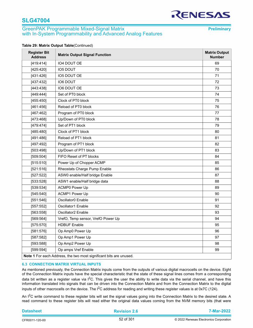
Datasheet 7-Mar-2022
CFR0011-120-00
Revision 2.6
52 of 301 © 2022 Renesas Electronics Corporation
SLG47004
GreenPAK Programmable Mixed-Signal Matrix with In-System Programmability and Advanced Analog Features
Preliminary
6.3 CONNECTION MATRIX VIRTUAL INPUTS
As mentioned previously, the Connection Matrix inputs come from the outputs of various digital macrocells on the device. Eightof the Connection Matrix inputs have the special characteristic that the state of these signal lines comes from a corresponding
data bit written as a register value via I2C. This gives the user the ability to write data via the serial channel, and have thisinformation translated into signals that can be driven into the Connection Matrix and from the Connection Matrix to the digital
inputs of other macrocells on the device. The I2C address for reading and writing these register values is at 0x7C (124).
An I2C write command to these register bits will set the signal values going into the Connection Matrix to the desired state. Aread command to these register bits will read either the original data values coming from the NVM memory bits (that were
[419:414] IO4 DOUT OE 69
[425:420] IO5 DOUT 70
[431:426] IO5 DOUT OE 71
[437:432] IO6 DOUT 72
[443:438] IO6 DOUT OE 73
[449:444] Set of PT0 block 74
[455:450] Clock of PT0 block 75
[461:456] Reload of PT0 block 76
[467:462] Program of PT0 block 77
[473:468] Up/Down of PT0 block 78
[479:474] Set of PT1 block 79
[485:480] Clock of PT1 block 80
[491:486] Reload of PT1 block 81
[497:492] Program of PT1 block 82
[503:498] Up/Down of PT1 block 83
[509:504] FIFO Reset of PT blocks 84
[515:510] Power Up of Chopper ACMP 85
[521:516] Rheostats Charge Pump Enable 86
[527:522] ASW0 enable/Half bridge Enable 87
[533:528] ASW1 enable/Half bridge data 88
[539:534] ACMP0 Power Up 89
[545:540] ACMP1 Power Up 90
[551:546] Oscillator0 Enable 91
[557:552] Oscillator1 Enable 92
[563:558] Oscillator2 Enable 93
[569:564] VrefO, Temp sensor, VrefO Power Up 94
[575:570] HDBUF Enable 95
[581:576] Op Amp0 Power Up 96
[587:582] Op Amp1 Power Up 97
[593:588] Op Amp2 Power Up 98
[599:594] Op amps Vref Enable 99
Note 1 For each Address, the two most significant bits are unused.
Table 29: Matrix Output Table(Continued)
Register Bit
AddressMatrix Output Signal Function
Matrix Output
Number

Datasheet 7-Mar-2022
CFR0011-120-00
Revision 2.6
53 of 301 © 2022 Renesas Electronics Corporation
SLG47004
GreenPAK Programmable Mixed-Signal Matrix with In-System Programmability and Advanced Analog Features
Preliminary
loaded during the initial device startup), or the values from a previous write command (if that has happened).
See Table 30.
6.4 CONNECTION MATRIX VIRTUAL OUTPUTS
The digital outputs of the various macrocells are routed to the Connection Matrix to enable interconnections to the inputs of othermacrocells in the device. At the same time, it is possible to read the state of each of the macrocell outputs as a register value viaI2C. This option, called Connection Matrix Virtual Outputs, allows the user to remotely read the values of each macrocell output.The I2C addresses for reading these register values are bytes 0xC4 (196) to 0xCA (202). Write commands to these same registervalues will be ignored (with the exception of the Virtual Input register bits at byte 0x7C (124)).
Table 30: Connection Matrix Virtual Inputs
Matrix Input
NumberMatrix Input Signal Function
Register Bit
Addresses (d)
32 I2C_virtual_0 Input [992]
33 I2C_virtual_1 Input [993]
34 I2C_virtual_2 Input [994]
35 I2C_virtual_3 Input [995]
36 I2C_virtual_4 Input [996]
37 I2C_virtual_5 Input [997]
38 I2C_virtual_6 Input [998]
39 I2C_virtual_7 Input [999]
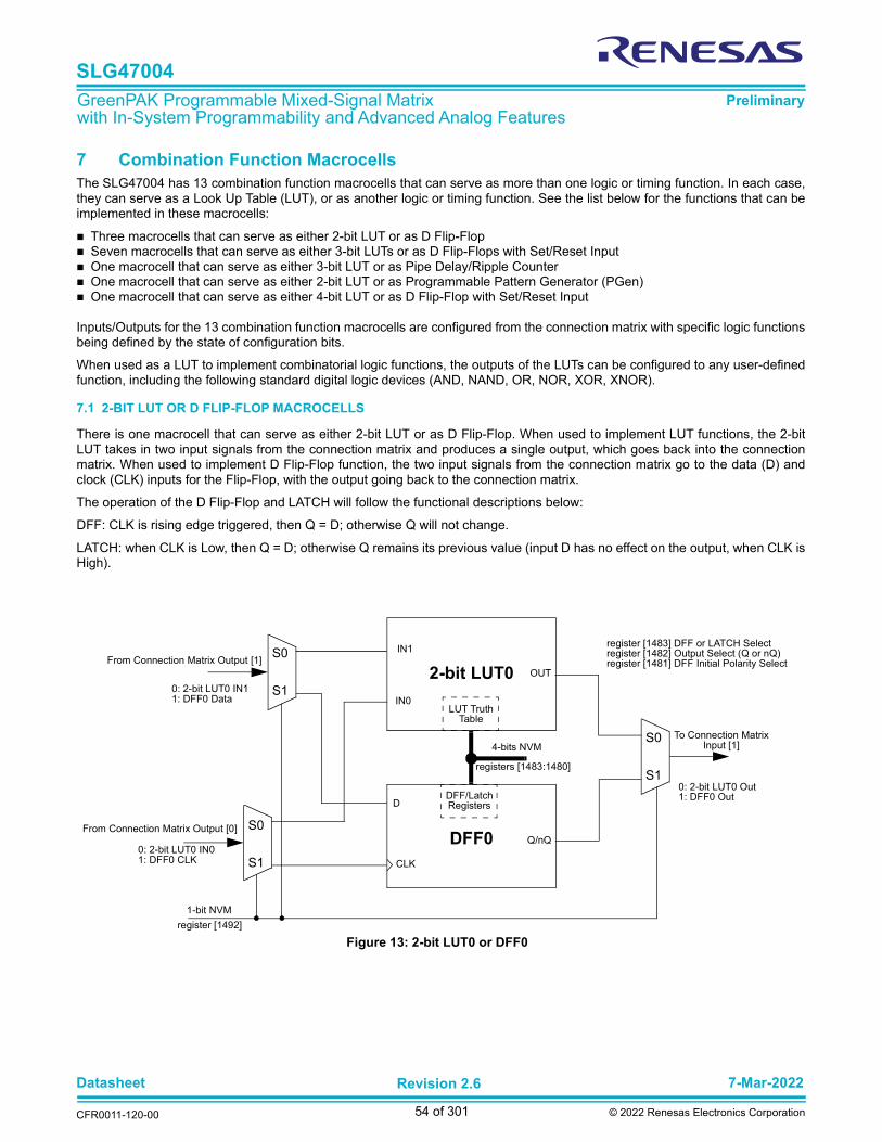
Datasheet 7-Mar-2022
CFR0011-120-00
Revision 2.6
54 of 301 © 2022 Renesas Electronics Corporation
SLG47004
GreenPAK Programmable Mixed-Signal Matrix with In-System Programmability and Advanced Analog Features
Preliminary
7 Combination Function Macrocells
The SLG47004 has 13 combination function macrocells that can serve as more than one logic or timing function. In each case,they can serve as a Look Up Table (LUT), or as another logic or timing function. See the list below for the functions that can beimplemented in these macrocells:
Three macrocells that can serve as either 2-bit LUT or as D Flip-Flop Seven macrocells that can serve as either 3-bit LUTs or as D Flip-Flops with Set/Reset Input One macrocell that can serve as either 3-bit LUT or as Pipe Delay/Ripple Counter One macrocell that can serve as either 2-bit LUT or as Programmable Pattern Generator (PGen) One macrocell that can serve as either 4-bit LUT or as D Flip-Flop with Set/Reset Input
Inputs/Outputs for the 13 combination function macrocells are configured from the connection matrix with specific logic functionsbeing defined by the state of configuration bits.
When used as a LUT to implement combinatorial logic functions, the outputs of the LUTs can be configured to any user-definedfunction, including the following standard digital logic devices (AND, NAND, OR, NOR, XOR, XNOR).
7.1 2-BIT LUT OR D FLIP-FLOP MACROCELLS
There is one macrocell that can serve as either 2-bit LUT or as D Flip-Flop. When used to implement LUT functions, the 2-bitLUT takes in two input signals from the connection matrix and produces a single output, which goes back into the connectionmatrix. When used to implement D Flip-Flop function, the two input signals from the connection matrix go to the data (D) andclock (CLK) inputs for the Flip-Flop, with the output going back to the connection matrix.
The operation of the D Flip-Flop and LATCH will follow the functional descriptions below:
DFF: CLK is rising edge triggered, then Q = D; otherwise Q will not change.
LATCH: when CLK is Low, then Q = D; otherwise Q remains its previous value (input D has no effect on the output, when CLK isHigh).
Figure 13: 2-bit LUT0 or DFF0
DFF0
CLK
D
2-bit LUT0 OUT
IN0
IN1
To Connection MatrixInput [1]4-bits NVM
From Connection Matrix Output [1]
1-bit NVM
registers [1483:1480]
register [1492]
From Connection Matrix Output [0]Q/nQ
register [1483] DFF or LATCH Selectregister [1482] Output Select (Q or nQ)register [1481] DFF Initial Polarity Select
LUT Truth Table
DFF/LatchRegisters
S0
S1
S0
S1
S0
S1
0: 2-bit LUT0 IN11: DFF0 Data
0: 2-bit LUT0 Out1: DFF0 Out
0: 2-bit LUT0 IN01: DFF0 CLK

Datasheet 7-Mar-2022
CFR0011-120-00
Revision 2.6
55 of 301 © 2022 Renesas Electronics Corporation
SLG47004
GreenPAK Programmable Mixed-Signal Matrix with In-System Programmability and Advanced Analog Features
Preliminary
Figure 14: 2-bit LUT1 or DFF1
Figure 15: 2-bit LUT2 or DFF2
DFF1
CLK
D
2-bit LUT1 OUT
IN0
IN1
To Connection MatrixInput [2]4-bits NVM
From Connection Matrix Output [3]
1-bit NVM
registers [1487:1484]
register [1493]
From Connection Matrix Output [2]Q/nQ
register [1487] DFF or LATCH Selectregister [1486] Output Select (Q or nQ)register [1485] DFF Initial Polarity Select
LUT Truth Table
DFF/LatchRegisters
S0
S1
S0
S1
S0
S1
0: 2-bit LUT1 IN11: DFF1 Data
0: 2-bit LUT1 Out1: DFF1 Out
0: 2-bit LUT1 IN01: DFF1 CLK
DFF2
CLK
D
2-bit LUT2 OUT
IN0
IN1
To Connection MatrixInput [3]4-bits NVM
From Connection Matrix Output [5]
1-bit NVM
registers [1491:1488]
register [1494]
From Connection Matrix Output [4]Q/nQ
register [1491] DFF or LATCH Selectregister [1490] Output Select (Q or nQ)register [1489] DFF Initial Polarity Select
LUT Truth Table
DFF/LatchRegisters
S0
S1
S0
S1
S0
S1
0: 2-bit LUT2 IN11: DFF2 Data
0: 2-bit LUT2 Out1: DFF2 Out
0: 2-bit LUT2 IN01: DFF2 CLK

Datasheet 7-Mar-2022
CFR0011-120-00
Revision 2.6
56 of 301 © 2022 Renesas Electronics Corporation
SLG47004
GreenPAK Programmable Mixed-Signal Matrix with In-System Programmability and Advanced Analog Features
Preliminary
7.1.1 2-Bit LUT or D Flip-Flop Macrocell Used as 2-Bit LUT
This macrocell, when programmed for a LUT function, uses a 4-bit register to define their output function:
2-Bit LUT0 is defined by registers [1483:1480]
2-Bit LUT1 is defined by registers [1487:1484]
2-Bit LUT2 is defined by registers [1491:1488]
Table 34 shows the register bits for the standard digital logic devices (AND, NAND, OR, NOR, XOR, XNOR) that can be createdwithin each of the 2-bit LUT logic cells.
Table 34: 2-bit LUT Standard Digital Functions
Function MSB LSB
AND-2 1 0 0 0
NAND-2 0 1 1 1
OR-2 1 1 1 0
NOR-2 0 0 0 1
XOR-2 0 1 1 0
XNOR-2 1 0 0 1
Table 31: 2-bit LUT0 Truth Table
IN1 IN0 OUT
0 0 register [1480] LSB
0 1 register [1481]
1 0 register [1482]
1 1 register [1483] MSB
Table 32: 2-bit LUT1 Truth Table
IN1 IN0 OUT
0 0 register [1484] LSB
0 1 register [1485]
1 0 register [1486]
1 1 register [1487] MSB
Table 33: 2-bit LUT2 Truth Table
IN1 IN0 OUT
0 0 register [1488] LSB
0 1 register [1489]
1 0 register [1490]
1 1 register [1491] MSB

Datasheet 7-Mar-2022
CFR0011-120-00
Revision 2.6
57 of 301 © 2022 Renesas Electronics Corporation
SLG47004
GreenPAK Programmable Mixed-Signal Matrix with In-System Programmability and Advanced Analog Features
Preliminary
7.1.2 Initial Polarity Operations
7.2 2-BIT LUT OR PROGRAMMABLE PATTERN GENERATOR
The SLG47004 has one combination function macrocell that can serve as a logic or a timing function. This macrocell can serveas a Look Up Table (LUT), or a Programmable Pattern Generator (PGen).
When used to implement LUT functions, the 2-bit LUT takes in two input signals from the connection matrix and produces asingle output, which goes back into the connection matrix. When used as a LUT to implement combinatorial logic functions, theoutputs of the LUT can be configured to any user defined function, including the following standard digital logic devices (AND,NAND, OR, NOR, XOR, XNOR). The user can also define the combinatorial relationship between inputs and outputs to be anyselectable function.
It is possible to define the RST level for the PGen macrocell. There are both high level reset (RST) and a low level reset (nRST)options available, which are selected by register [1517]. When operating as the Programmable Pattern Generator, the output ofthe macrocell will clock out a sequence of two to sixteen bits that are user selectable in their bit values, and user selectable inthe number of bits (up to sixteen) that are output before the pattern repeats.
Figure 16: DFF Polarity Operations
VDD
Data
Clock
POR
Q with nReset (Case 1)
Initial Polarity: High
Q with nReset (Case 1)
Initial Polarity: Low
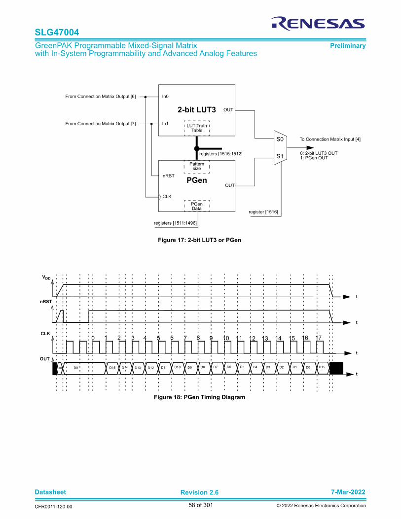
Datasheet 7-Mar-2022
CFR0011-120-00
Revision 2.6
58 of 301 © 2022 Renesas Electronics Corporation
SLG47004
GreenPAK Programmable Mixed-Signal Matrix with In-System Programmability and Advanced Analog Features
Preliminary
Figure 17: 2-bit LUT3 or PGen
Figure 18: PGen Timing Diagram
PGenOUT
CLK
nRST
2-bit LUT3 OUT
To Connection Matrix Input [4]
From Connection Matrix Output [6]
registers [1515:1512]
register [1516]
From Connection Matrix Output [7]
In0
In1
registers [1511:1496]
LUT Truth Table
Patternsize
PGenData
0: 2-bit LUT3 OUT1: PGen OUT
S0
S1
VDD
OUT
D15
CLK
D0
0 1
t
2 3 4 5 6 7 8 9 10 11 12 13 14 15 16 17
D14D0 D13 D12 D11 D10 D9 D8 D7 D6 D5 D4 D3 D2 D1 D0 D15
t
t
t
nRST
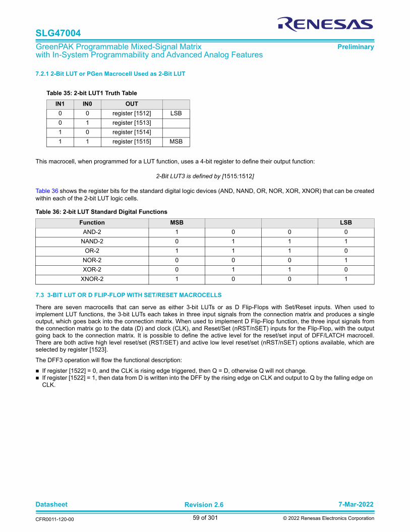
Datasheet 7-Mar-2022
CFR0011-120-00
Revision 2.6
59 of 301 © 2022 Renesas Electronics Corporation
SLG47004
GreenPAK Programmable Mixed-Signal Matrix with In-System Programmability and Advanced Analog Features
Preliminary
7.2.1 2-Bit LUT or PGen Macrocell Used as 2-Bit LUT
This macrocell, when programmed for a LUT function, uses a 4-bit register to define their output function:
2-Bit LUT3 is defined by [1515:1512]
Table 36 shows the register bits for the standard digital logic devices (AND, NAND, OR, NOR, XOR, XNOR) that can be createdwithin each of the 2-bit LUT logic cells.
7.3 3-BIT LUT OR D FLIP-FLOP WITH SET/RESET MACROCELLS
There are seven macrocells that can serve as either 3-bit LUTs or as D Flip-Flops with Set/Reset inputs. When used toimplement LUT functions, the 3-bit LUTs each takes in three input signals from the connection matrix and produces a singleoutput, which goes back into the connection matrix. When used to implement D Flip-Flop function, the three input signals fromthe connection matrix go to the data (D) and clock (CLK), and Reset/Set (nRST/nSET) inputs for the Flip-Flop, with the outputgoing back to the connection matrix. It is possible to define the active level for the reset/set input of DFF/LATCH macrocell.There are both active high level reset/set (RST/SET) and active low level reset/set (nRST/nSET) options available, which areselected by register [1523].
The DFF3 operation will flow the functional description:
If register [1522] = 0, and the CLK is rising edge triggered, then Q = D, otherwise Q will not change. If register [1522] = 1, then data from D is written into the DFF by the rising edge on CLK and output to Q by the falling edge on
CLK.
Table 36: 2-bit LUT Standard Digital Functions
Function MSB LSB
AND-2 1 0 0 0
NAND-2 0 1 1 1
OR-2 1 1 1 0
NOR-2 0 0 0 1
XOR-2 0 1 1 0
XNOR-2 1 0 0 1
Table 35: 2-bit LUT1 Truth Table
IN1 IN0 OUT
0 0 register [1512] LSB
0 1 register [1513]
1 0 register [1514]
1 1 register [1515] MSB

Datasheet 7-Mar-2022
CFR0011-120-00
Revision 2.6
60 of 301 © 2022 Renesas Electronics Corporation
SLG47004
GreenPAK Programmable Mixed-Signal Matrix with In-System Programmability and Advanced Analog Features
Preliminary
Figure 19: 3-bit LUT0 or DFF3
DFF
CLK
D
8-bits NVM
1-bit NVM
3-bit LUT0 OUTIN1
IN2
IN0
nRST/nSET
From Connection Matrix Output [10]
From Connection Matrix Output [9]
From Connection Matrix Output [8]
registers [1527:1520]
register [1518]
To Connection MatrixInput [5]
Q/nQ
LUT Truth Table
DFF/Latch Registers
S0
S1
S0
S1
S0
S1
S0
S1
D Q
CL
D Q
CL
0
1
DFF
register [1522]
nRST/nSET
nRST/nSET
register [1527] DFF or Latch Selectregister [1526] Output Select (Q or nQ)register [1525] DFF Initial Polarity Selectregister [1524] DFF nRST or nSET Selectregister [1523] Active level selection for RST/SETregister [1522] Q1 or Q2 Select

Datasheet 7-Mar-2022
CFR0011-120-00
Revision 2.6
61 of 301 © 2022 Renesas Electronics Corporation
SLG47004
GreenPAK Programmable Mixed-Signal Matrix with In-System Programmability and Advanced Analog Features
Preliminary
Figure 20: 3-bit LUT1 or DFF4
Figure 21: 3-bit LUT2 or DFF5
DFF4
CLK
D
8-bits NVM
1-bit NVM
3-bit LUT1 OUTIN1
IN2
IN0
nRST/nSET
From Connection Matrix Output [13]
From Connection Matrix Output [12]
From Connection Matrix Output [11]
registers [1535:1528]
register [1519]
To Connection Matrix Input [6]
Q/nQ
register [1535] DFF or LATCH Selectregister [1534] Output Select (Q or nQ)register [1533] DFF Initial Polarity Selectregister [1532] DFF nRST or nSET Selectregister [1531] Active level selection for RST/SET
LUT Truth Table
DFF/LatchRegisters
S0
S1
S0
S1
S0
S1
S0
S1
DFF5
CLK
D
To Connection Matrix Input [7]
8-bits NVM
From ConnectionMatrix Output [16]
1-bit NVM
3-bit LUT2 OUTIN1
IN2
IN0
nRST/nSET
From Connection Matrix Output [15]
From Connection Matrix Output [14]
registers [791:784]
register [824]
Q/nQ
register [791] DFF or LATCH Selectregister [790] Output Select (Q or nQ)register [789] DFF Initial Polarity Selectregister [788] DFF nRST or nSET Selectregister [787] Active level selection for RST/SET
LUT Truth Table
DFF/LatchRegisters
S0
S1
S0
S1
S0
S1
S0
S1

Datasheet 7-Mar-2022
CFR0011-120-00
Revision 2.6
62 of 301 © 2022 Renesas Electronics Corporation
SLG47004
GreenPAK Programmable Mixed-Signal Matrix with In-System Programmability and Advanced Analog Features
Preliminary
Figure 22: 3-bit LUT3 or DFF6
Figure 23: 3-bit LUT4 or DFF7
DFF6
CLK
D
8-bits NVM
1-bit NVM
3-bit LUT3 OUTIN1
IN2
IN0
nRST/nSET
From Connection Matrix Output [19]
From Connection Matrix Output [18]
From Connection Matrix Output [17]
registers [799:792]
register [825]
To Connection Matrix Input [8]
Q/nQ
LUT Truth Table
DFF Registers
S0
S1
S0
S1
S0
S1
S0
S1
register [799] DFF or LATCH Selectregister [798] Output Select (Q or nQ)register [797] DFF Initial Polarity Selectregister [796] DFF nRST or nSET Selectregister [795] Active level selection for RST/SET
DFF7
CLK
D
8-bits NVM
1-bit NVM
3-bit LUT4 OUTIN1
IN2
IN0
nRST/nSET
From Connection Matrix Output [22]
From Connection Matrix Output [21]
From Connection Matrix Output [20]
registers [807:800]
registers [826]
To Connection Matrix Input [9]
Q/nQ
LUT Truth Table
DFF/LatchRegisters
S0
S1
S0
S1
S0
S1
S0
S1
register [807] DFF or LATCH Selectregister [806] Output Select (Q or nQ)register [805] DFF Initial Polarity Selectregister [804] DFF nRST or nSET Selectregister [803] Active level selection for RST/SET

Datasheet 7-Mar-2022
CFR0011-120-00
Revision 2.6
63 of 301 © 2022 Renesas Electronics Corporation
SLG47004
GreenPAK Programmable Mixed-Signal Matrix with In-System Programmability and Advanced Analog Features
Preliminary
Figure 24: 3-bit LUT5 or DFF8
Figure 25: 3-bit LUT6 or DFF9
DFF8
CLK
D
8-bits NVM
1-bit NVM
3-bit LUT5 OUTIN1
IN2
IN0
nRST/nSET
From Connection Matrix Output [25]
From Connection Matrix Output [24]
From Connection Matrix Output [23]
registers [815:808]
register [827]
To Connection Matrix Input [10]
Q/nQ
LUT Truth Table
DFF Registers
S0
S1
S0
S1
S0
S1
S0
S1
register [815] DFF or LATCH Selectregister [814] Output Select (Q or nQ)register [813] DFF Initial Polarity Selectregister [812] DFF nRST or nSET Selectregister [811] Active level selection for RST/SET
DFF9
CLK
D
8-bits NVM
1-bit NVM
3-bit LUT6 OUTIN1
IN2
IN0
nRST/nSET
From Connection Matrix Output [28]
From Connection Matrix Output [27]
From Connection Matrix Output [26]
registers [823:816]
register [828]
To Connection Matrix Input [11]
Q/nQ
LUT Truth Table
DFF Registers
S0
S1
S0
S1
S0
S1
S0
S1
register [823] DFF or LATCH Selectregister [822] Output Select (Q or nQ)register [821] DFF Initial Polarity Selectregister [820] DFF nRST or nSET Selectregister [819] Active level selection for RST/SET

Datasheet 7-Mar-2022
CFR0011-120-00
Revision 2.6
64 of 301 © 2022 Renesas Electronics Corporation
SLG47004
GreenPAK Programmable Mixed-Signal Matrix with In-System Programmability and Advanced Analog Features
Preliminary
7.3.1 3-Bit LUT or D Flip-Flop Macrocells Used as 3-Bit LUTs
Table 37: 3-bit LUT0 Truth Table
IN2 IN1 IN0 OUT
0 0 0 register [1520] LSB
0 0 1 register [1521]
0 1 0 register [1522]
0 1 1 register [1523]
1 0 0 register [1524]
1 0 1 register [1525]
1 1 0 register [1526]
1 1 1 register [1527] MSB
Table 38: 3-bit LUT1 Truth Table
IN2 IN1 IN0 OUT
0 0 0 register [1528] LSB
0 0 1 register [1529]
0 1 0 register [1530]
0 1 1 register [1531]
1 0 0 register [1532]
1 0 1 register [1533]
1 1 0 register [1534]
1 1 1 register [1535] MSB
Table 39: 3-bit LUT2 Truth Table
IN2 IN1 IN0 OUT
0 0 0 register [784] LSB
0 0 1 register [785]
0 1 0 register [786]
0 1 1 register [787]
1 0 0 register [788]
1 0 1 register [789]
1 1 0 register [790]
1 1 1 register [791] MSB
Table 40: 3-bit LUT3 Truth Table
IN2 IN1 IN0 OUT
0 0 0 register [792] LSB
0 0 1 register [793]
0 1 0 register [794]
0 1 1 register [795]
1 0 0 register [796]
1 0 1 register [797]
1 1 0 register [798]
1 1 1 register [799] MSB
Table 41: 3-bit LUT4 Truth Table
IN2 IN1 IN0 OUT
0 0 0 register [800] LSB
0 0 1 register [801]
0 1 0 register [802]
0 1 1 register [803]
1 0 0 register [804]
1 0 1 register [805]
1 1 0 register [806]
1 1 1 register [807] MSB
Table 42: 3-bit LUT5 Truth Table
IN2 IN1 IN0 OUT
0 0 0 register [808] LSB
0 0 1 register [809]
0 1 0 register [810]
0 1 1 register [811]
1 0 0 register [812]
1 0 1 register [813]
1 1 0 register [814]
1 1 1 register [815] MSB
Table 43: 3-bit LUT6 Truth Table
IN2 IN1 IN0 OUT
0 0 0 register [816] LSB
0 0 1 register [817]
0 1 0 register [818]
0 1 1 register [819]
1 0 0 register [820]
1 0 1 register [821]
1 1 0 register [822]
1 1 1 register [823] MSB

Datasheet 7-Mar-2022
CFR0011-120-00
Revision 2.6
65 of 301 © 2022 Renesas Electronics Corporation
SLG47004
GreenPAK Programmable Mixed-Signal Matrix with In-System Programmability and Advanced Analog Features
Preliminary
Each macrocell, when programmed for a LUT function, uses an 8-bit register to define their output function:
3-Bit LUT0 is defined by registers [1527:1520]
3-Bit LUT1 is defined by registers [1535:1528]
3-Bit LUT2 is defined by registers [791:784]
3-Bit LUT3 is defined by registers [799:792]
3-Bit LUT4 is defined by registers [807:800]
3-Bit LUT5 is defined by registers [815:808]
3-Bit LUT6 is defined by registers [823:816]
Table 44 shows the register bits for the standard digital logic devices (AND, NAND, OR, NOR, XOR, XNOR) that can be createdwithin each of the four 3-bit LUT logic cells.
Table 44: 3-bit LUT Standard Digital Functions
Function MSB LSB
AND-3 1 0 0 0 0 0 0 0
NAND-3 0 1 1 1 1 1 1 1
OR-3 1 1 1 1 1 1 1 0
NOR-3 0 0 0 0 0 0 0 1
XOR-3 1 0 0 1 0 1 1 0
XNOR-3 0 1 1 0 1 0 0 1

Datasheet 7-Mar-2022
CFR0011-120-00
Revision 2.6
66 of 301 © 2022 Renesas Electronics Corporation
SLG47004
GreenPAK Programmable Mixed-Signal Matrix with In-System Programmability and Advanced Analog Features
Preliminary
7.3.2 Initial Polarity Operations
Figure 26: DFF Polarity Operations with nReset
VDD
Data
Clock
POR
nReset (Case 1)
Q with nReset (Case 2)
Initial Polarity: High
Initial Polarity: Low
nReset (Case 1)
Q with nReset (Case 1)
nReset (Case 2)
Q with nReset (Case 2)
Q with nReset (Case 1)
nReset (Case 2)
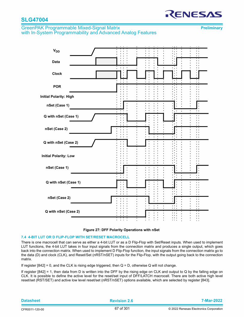
Datasheet 7-Mar-2022
CFR0011-120-00
Revision 2.6
67 of 301 © 2022 Renesas Electronics Corporation
SLG47004
GreenPAK Programmable Mixed-Signal Matrix with In-System Programmability and Advanced Analog Features
Preliminary
7.4 4-BIT LUT OR D FLIP-FLOP WITH SET/RESET MACROCELL
There is one macrocell that can serve as either a 4-bit LUT or as a D Flip-Flop with Set/Reset inputs. When used to implementLUT functions, the 4-bit LUT takes in four input signals from the connection matrix and produces a single output, which goesback into the connection matrix. When used to implement D Flip-Flop function, the input signals from the connection matrix go tothe data (D) and clock (CLK), and Reset/Set (nRST/nSET) inputs for the Flip-Flop, with the output going back to the connectionmatrix.
If register [842] = 0, and the CLK is rising edge triggered, then Q = D, otherwise Q will not change.
If register [842] = 1, then data from D is written into the DFF by the rising edge on CLK and output to Q by the falling edge onCLK. It is possible to define the active level for the reset/set input of DFF/LATCH macrocell. There are both active high levelreset/set (RST/SET) and active low level reset/set (nRST/nSET) options available, which are selected by register [843].
Figure 27: DFF Polarity Operations with nSet
VDD
Data
Clock
POR
nSet (Case 1)
Q with nSet (Case 2)
Initial Polarity: High
Initial Polarity: Low
nSet (Case 1)
Q with nSet (Case 1)
nSet (Case 2)
Q with nSet (Case 2)
Q with nSet (Case 1)
nSet (Case 2)

Datasheet 7-Mar-2022
CFR0011-120-00
Revision 2.6
68 of 301 © 2022 Renesas Electronics Corporation
SLG47004
GreenPAK Programmable Mixed-Signal Matrix with In-System Programmability and Advanced Analog Features
Preliminary
7.4.1 4-Bit LUT Macrocell Used as 4-Bit LUT
Figure 28: 4-bit LUT0 or DFF10
DFF10
CLK
D
16-bits NVM
1-bit NVM
4-bit LUT0 OUTIN1
IN2
IN0
From Connection Matrix Output [52]
From Connection Matrix Output [51]
From Connection Matrix Output [50]
registers [847:832]
register [829]
To Connection MatrixInput [29]
Q/nQ
LUT Truth Table
DFF/LatchRegisters
S0
S1
S0
S1
S0
S1
S0
S1
Q1/Q2Select
register [842]
IN3
From Connection Matrix Output [53] S0
S1
register [847] DFF or LATCH Selectregister [846] Output Select (Q or nQ)register [845] DFF Initial Polarity Selectregister [844] DFF nRST or nSET Selectregister [843]Active level selection for RST/SETregister [842] Q1 or Q2 Select
nRST/nSETRST/SET
Table 45: 4-bit LUT0 Truth Table
IN3 IN2 IN1 IN0 OUT
0 0 0 0 register [832] LSB
0 0 0 1 register [833]
0 0 1 0 register [834]
0 0 1 1 register [835]
0 1 0 0 register [836]
0 1 0 1 register [837]
0 1 1 0 register [838]
0 1 1 1 register [839]
1 0 0 0 register [840]
1 0 0 1 register [841]
1 0 1 0 register [842]
1 0 1 1 register [843]
1 1 0 0 register [844]
1 1 0 1 register [845]
1 1 1 0 register [846]
1 1 1 1 register [847] MSB

Datasheet 7-Mar-2022
CFR0011-120-00
Revision 2.6
69 of 301 © 2022 Renesas Electronics Corporation
SLG47004
GreenPAK Programmable Mixed-Signal Matrix with In-System Programmability and Advanced Analog Features
Preliminary
This macrocell, when programmed for a LUT function, uses a 16-bit register to define their output function:
4-Bit LUT0 is defined by registers [847:832]
7.5 3-BIT LUT OR PIPE DELAY/RIPPLE COUNTER MACROCELL
There is one macrocell that can serve as either a 3-bit LUT or as a Pipe Delay/Ripple Counter.
When used to implement LUT functions, the 3-bit LUT takes in three input signals from the connection matrix and produces asingle output, which goes back into the connection matrix.
When used as a Pipe Delay, there are three inputs signals from the matrix, Input (IN), Clock (CLK), and Reset (nRST). The PipeDelay cell is built from 16 D Flip-Flop logic cells that provide the three delay options, two of which are user selectable. The DFFcells are tied in series where the output (Q) of each delay cell goes to the next DFF cell input (IN). Both of the two outputs (OUT0and OUT1) provide user selectable options for 1 to 16 stages of delay. There are delay output points for each set of the OUT0and OUT1 outputs to a 4-input mux that is controlled by registers [851:848] for OUT0 and registers [855:852] for OUT1. The 4-input MUX is used to control the selection of the amount of delay.
The overall time of the delay is based on the clock used in the SLG47004 design. Each DFF cell has a time delay of the inverseof the clock time (either external clock or the internal Oscillator within the SLG47004). The sum of the number of DFF cells usedwill be the total time delay of the Pipe Delay logic cell. OUT1 Output can be inverted (as selected by register [859]).
In the Ripple Counter mode, there are 3 options for setting, which use 7 bits. There are 3 bits to set nSET value (SV) in rangefrom 0 to 7. It is a value, which will be set into the Ripple Counter outputs when nSET input goes LOW. End value (EV) will use3 bits for setting outputs code, which will be last code in the cycle. After reaching the EV, the Ripple Counter goes to the first codeby the rising edge on CLK input. The Functionality mode option uses 1 bit. This setting defines how exactly Ripple Counter willoperate.
The user can select one of the functionality modes by register: RANGE or FULL. If the RANGE option is selected, the count startsfrom SV. If UP input is LOW the count goes down: SV→EV→EV-1 to SV+1→SV, and others (if SV is smaller than EV), or SV→SV-1 to EV+1→EV→SV (if SV is bigger than EV). If UP input is HIGH, count starts from SV up to EV, and others.
In the FULL range configuration the Ripple Counter functions as follows. If UP input is LOW, the count starts from SV and goesdown to 0. Then current counter value jumps to EV and goes down to 0, and others.
If UP input is HIGH, count goes up starting from SV. Then current counter value jumps to 0 and counts up to EV, and others. SeeRipple Counter functionality example in Figure 30.
Every step is executed by the rising edge on CLK input.
Table 46: 4-bit LUT Standard Digital Functions
Function MSB LSB
AND-4 1 0 0 0 0 0 0 0 0 0 0 0 0 0 0 0
NAND-4 0 1 1 1 1 1 1 1 1 1 1 1 1 1 1 1
OR-4 1 1 1 1 1 1 1 1 1 1 1 1 1 1 1 0
NOR-4 0 0 0 0 0 0 0 0 0 0 0 0 0 0 0 1
XOR-4 0 1 1 0 1 0 0 1 1 0 0 1 0 1 1 0
XNOR-4 1 0 0 1 0 1 1 0 0 1 1 0 1 0 0 1

Datasheet 7-Mar-2022
CFR0011-120-00
Revision 2.6
70 of 301 © 2022 Renesas Electronics Corporation
SLG47004
GreenPAK Programmable Mixed-Signal Matrix with In-System Programmability and Advanced Analog Features
Preliminary
Figure 29: 3-bit LUT13/Pipe Delay/Ripple Counter
3-bit LUT13 OUTIN1
IN0
registers [855:848]
From Connection Matrix Output [47]
From Connection Matrix Output [48]
IN2
From Connection Matrix Output [49]
16 Flip-FlopsnRST
IN
CLK
From Connection Matrix Output [47]
From Connection Matrix Output [48]
From Connection Matrix Output [49]
registers [855:852]
registers [851:848]
0
1
To Connection Matrix Input [26]
0
1
regi
ste
r [8
58]
0
1
register [858]
0
1 To Connection Matrix Input [27]
UP/DOWNControl
SETControl
Mode & SET/END Value Control
3 Flip-Flops
D Q
nQCL
D Q
nQCL
D Q
nQCL
DFF1
DFF2
DFF3
Ripple Counter
Pipe Delay
From Connection Matrix Output [47]
From Connection Matrix Output [49]
From Connection Matrix Output [48]
UP
CLK
nSET
registers [854:848]
OUT0
OUT1
OUT2
OUT1
OUT0
register [857]
OUT0
OUT1
register [859]
To Connection Matrix Input[28]
register [858]
0
1
OUT2
1 Pipe OUT

Datasheet 7-Mar-2022
CFR0011-120-00
Revision 2.6
71 of 301 © 2022 Renesas Electronics Corporation
SLG47004
GreenPAK Programmable Mixed-Signal Matrix with In-System Programmability and Advanced Analog Features
Preliminary
7.5.1 3-Bit LUT or Pipe Delay Macrocells Used as 3-Bit LUT
Figure 30: Example: Ripple Counter Functionality
Table 47: 3-bit LUT13 Truth Table
IN2 IN1 IN0 OUT
0 0 0 register [848]
0 0 1 register [849]
0 1 0 register [850]
0 1 1 register [851]
1 0 0 register [852]
1 0 1 register [853]
1 1 0 register [854]
1 1 1 register [855]
Datasheet 7-Mar-2022
CFR0011-120-00
Revision 2.6
72 of 301 © 2022 Renesas Electronics Corporation
SLG47004
GreenPAK Programmable Mixed-Signal Matrix with In-System Programmability and Advanced Analog Features
Preliminary
Each macrocell, when programmed for a LUT function, uses an 8-bit register to define their output function:
3-Bit LUT13 is defined by registers [855:848]

Datasheet 7-Mar-2022
CFR0011-120-00
Revision 2.6
73 of 301 © 2022 Renesas Electronics Corporation
SLG47004
GreenPAK Programmable Mixed-Signal Matrix with In-System Programmability and Advanced Analog Features
Preliminary
8 Multi-Function Macrocells
The SLG47004 has seven Multi-Function macrocells that can serve as more than one logic or timing function. In each case, theycan serve as a LUT, DFF with flexible settings, or as CNT/DLY with multiple modes such as One Shot, Frequency Detect, EdgeDetect, and others. Also, the macrocell is capable to combine those functions: LUT/DFF connected to CNT/DLY or CNT/DLYconnected to LUT/DFF, see Figure 31.
See the list below for the functions that can be implemented in these macrocells:
Six macrocells that can serve as 3-bit LUTs/D Flip-Flops and as 8-Bit Counter/Delays One macrocell that can serve as a 4-bit LUT/D Flip-Flop and as 16-Bit Counter/Delay/FSM
Inputs/Outputs for the seven Multi-Function macrocells are configured from the connection matrix with specific logic functionsbeing defined by the state of NVM bits.
When used as a LUT to implement combinatorial logic functions, the outputs of the LUTs can be configured to any user definedfunction, including the following standard digital logic devices (AND, NAND, OR, NOR, XOR, XNOR).
8.1 3-BIT LUT OR DFF/LATCH WITH 8-BIT COUNTER/DELAY MACROCELLS
There are six macrocells that can serve as 3-bit LUTs/D Flip-Flops and as 8-Bit Counter/Delays.
When used to implement LUT functions, the 3-bit LUTs each takes in three input signals from the connection matrix and producesa single output, which goes back into the connection matrix or can be connected to CNT/DLY's input.
When used to implement D Flip-Flop function, the three input signals from the connection matrix go to the data (D), clock (CLK),and Reset/Set (nRST/nSET) inputs of the Flip-Flop, with the output going back to the connection matrix or to the CNT/DLY's input.
When used to implement Counter/Delays, each macrocell has a dedicated matrix input connection. For flexibility, each of thesemacrocells has a large selection of internal and external clock sources, as well as the option to chain from the output of theprevious (N-1) CNT/DLY macrocell, to implement longer count/delay circuits. These macrocells can also operate in a One-Shotmode, which will generate an output pulse of user-defined width. They can also operate in a Frequency Detection or EdgeDetection mode.
Counter/Delay macrocell has an initial value, which defines its initial value after SLG47004 is powered up. It is possible to selectinitial Low or initial High, as well as initial value defined by a Delay In signal.
For example, in case initial LOW option is used, the rising edge delay will start operation.
For timing diagrams refer to Section 8.3.
Note: After two DFF – counters initialize with counter data = 0 after POR.Initial state = 1 – counters initialize with counter data = 0 after POR.Initial state = 0 And After two DFF is bypass – counters initialize with counter data after POR.
Figure 31: Possible Connections Inside Multi-Function Macrocell
LUTor
DFFCNT/DLY
LUTor
DFFCNT/DLY
To Connection Matrix
To ConnectionMatrix
To Connection Matrix
To ConnectionMatrix
FromConnection
Matrix
FromConnection
Matrix

Datasheet 7-Mar-2022
CFR0011-120-00
Revision 2.6
74 of 301 © 2022 Renesas Electronics Corporation
SLG47004
GreenPAK Programmable Mixed-Signal Matrix with In-System Programmability and Advanced Analog Features
Preliminary
CNT5 and CNT6 current count value can be read via I2C. However, it is possible to change the counter data (value counter startsoperating from) for any macrocell using I2C write commands. In this mode, it is possible to load count data immediately (after twoDFF) or after counter ends counting. See Section 18.7.1 for further details.
8.1.1 3-Bit LUT or 8-Bit CNT/DLY Block Diagrams
Figure 32: 8-bit Multi-Function Macrocells Block Diagram (3-bit LUT7/DFF11, CNT/DLY1)
CNT/DLY1 OUT
ext_CLK
DLY_IN/CNT Reset
3-bit LUT7
OUT
IN0
IN1
8-bits NVM
IN2
registers [1391:1384]
From Connection Matrix Output [31]
To Connection Matrix Input [14]
LUT Truth Table
CNTData
S0
S1
ConfigData
registers [1255:1245],[1339:1338]
DFF/LATCH11
CLK
D
Q/nQ
DFF Registers
From Connection Matrix Output [30]
S0
S1
From Connection Matrix Output [29]
S0
S1
S0
S1
S0
S1
S2
S3
registers [1399:1392]
nRST/nSET
To Connection Matrix Input [15]
S0
S1
S0
S1
S0
S1
0S0
S1
S2
S30
LUT/DFF Sel
registers [1243:1240]
register [1244]
Mode Sel
register [1391] DFF or LATCH Selectregister [1390] Output Select (Q or nQ)register [1389] (nRST or nSET) frommatrix Outputregister [1388] DFF Initial Polarity Select
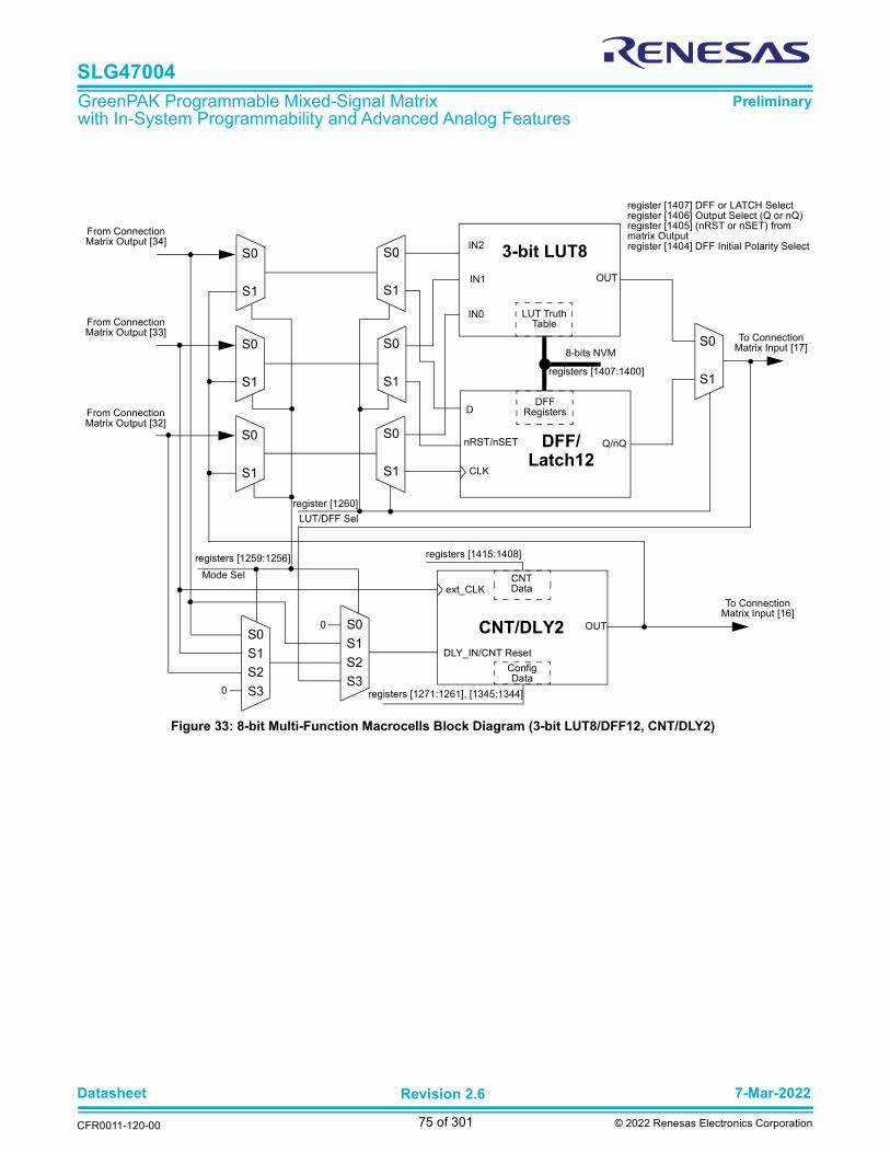
Datasheet 7-Mar-2022
CFR0011-120-00
Revision 2.6
75 of 301 © 2022 Renesas Electronics Corporation
SLG47004
GreenPAK Programmable Mixed-Signal Matrix with In-System Programmability and Advanced Analog Features
Preliminary
Figure 33: 8-bit Multi-Function Macrocells Block Diagram (3-bit LUT8/DFF12, CNT/DLY2)
CNT/DLY2 OUT
ext_CLK
DLY_IN/CNT Reset
3-bit LUT8
OUT
IN0
IN1
8-bits NVM
IN2
registers [1407:1400]
From Connection Matrix Output [34]
To Connection Matrix Input [16]
LUT Truth Table
CNTData
S0
S1
ConfigData
registers [1271:1261], [1345:1344]
DFF/Latch12
CLK
D
Q/nQ
DFF Registers
From Connection Matrix Output [33]
S0
S1
From Connection Matrix Output [32]
S0
S1
S0
S1
S0
S1
S2
S3
registers [1415:1408]
nRST/nSET
To Connection Matrix Input [17]
S0
S1
S0
S1
S0
S1
0S0
S1
S2
S30
LUT/DFF Sel
registers [1259:1256]
register [1260]
Mode Sel
register [1407] DFF or LATCH Selectregister [1406] Output Select (Q or nQ)register [1405] (nRST or nSET) frommatrix Outputregister [1404] DFF Initial Polarity Select

Datasheet 7-Mar-2022
CFR0011-120-00
Revision 2.6
76 of 301 © 2022 Renesas Electronics Corporation
SLG47004
GreenPAK Programmable Mixed-Signal Matrix with In-System Programmability and Advanced Analog Features
Preliminary
Figure 34: 8-bit Multi-Function Macrocells Block Diagram (3-bit LUT9/DFF13, CNT/DLY3)
CNT/DLY3 OUT
ext_CLK
DLY_IN/CNT Reset
3-bit LUT9
OUT
IN0
IN1
8-bits NVM
IN2
registers [1423:1416]
From Connection Matrix Output [37]
To Connection Matrix Input [18]
LUT Truth Table
CNTData
S0
S1
ConfigData
registers [1287:1277], [1347:1346]
DFF/Latch13
CLK
D
Q/nQ
DFF Registers
From Connection Matrix Output [36]
S0
S1
From Connection Matrix Output [35]
S0
S1
S0
S1
S0
S1
S2
S3
registers [1431:1424]
nRST/nSET
To Connection Matrix Input [19]
S0
S1
S0
S1
S0
S1
0S0
S1
S2
S30
LUT/DFF Sel
registers [1275:1272]
register [1276]
Mode Sel
register [1423] DFF or LATCH Selectregister [1422] Output Select (Q or nQ)register [1421] (nRST or nSET) frommatrix Outputregister [1420] DFF Initial Polarity Select

Datasheet 7-Mar-2022
CFR0011-120-00
Revision 2.6
77 of 301 © 2022 Renesas Electronics Corporation
SLG47004
GreenPAK Programmable Mixed-Signal Matrix with In-System Programmability and Advanced Analog Features
Preliminary
Figure 35: 8-bit Multi-Function Macrocells Block Diagram (3-bit LUT10/DFF14, CNT/DLY4)
CNT/DLY4 OUT
ext_CLK
DLY_IN/CNT Reset
3-bit LUT10
OUT
IN0
IN1
8-bits NVM
IN2
registers [1439:1432]
From Connection Matrix Output [40]
To Connection Matrix Input [20]
LUT Truth Table
CNTData
S0
S1
ConfigData
registers [1303:1293], [1349:1348]
DFF/Latch14
CLK
D
Q/nQ
DFF Registers
From Connection Matrix Output [39]
S0
S1
From Connection Matrix Output [38]
S0
S1
S0
S1
S0
S1
S2
S3
registers [1447:1440
nRST/nSET
To Connection Matrix Input [21]
S0
S1
S0
S1
S0
S1
0S0
S1
S2
S30
LUT/DFF Sel
registers [1291:1288]
register [1292]
Mode Sel
register [1439] DFF or LATCH Selectregister [1438] Output Select (Q or nQ)register [1437] (nRST or nSET) frommatrix Outputregister [1436] DFF Initial Polarity Select

Datasheet 7-Mar-2022
CFR0011-120-00
Revision 2.6
78 of 301 © 2022 Renesas Electronics Corporation
SLG47004
GreenPAK Programmable Mixed-Signal Matrix with In-System Programmability and Advanced Analog Features
Preliminary
Figure 36: 8-bit Multi-Function Macrocells Block Diagram (3-bit LUT11/DFF15, CNT/DLY5)
CNT/DLY5 OUT
ext_CLK
DLY_IN/CNT Reset
3-bit LUT11
OUT
IN0
IN1
8-bits NVM
IN2
registers [1455:1448]
From Connection Matrix Output [43]
To Connection Matrix Input [22]
LUT Truth Table
CNTData
S0
S1
ConfigData
registers [1319:1309], [1351:1350]
DFF/Latch15
CLK
D
Q/nQ
DFF Registers
From Connection Matrix Output [42]
S0
S1
From Connection Matrix Output [41]
S0
S1
S0
S1
S0
S1
S2
S3
registers [1463:1456]
nRST/nSET
To Connection Matrix Input [23]
S0
S1
S0
S1
S0
S1
0S0
S1
S2
S30
LUT/DFF Sel
registers [1307:1304]
register [1308]
Mode Sel
register [1455] DFF or LATCH Selectregister [1454] Output Select (Q or nQ)register [1453] (nRST or nSET) frommatrix Outputregister [1452] DFF Initial Polarity Select

Datasheet 7-Mar-2022
CFR0011-120-00
Revision 2.6
79 of 301 © 2022 Renesas Electronics Corporation
SLG47004
GreenPAK Programmable Mixed-Signal Matrix with In-System Programmability and Advanced Analog Features
Preliminary
As shown in Figure 32 to Figure 37 there is a possibility to use LUT/DFF and CNT/DLY simultaneously.
Note: It is not possible to use LUT and DFF at once, one of these macrocells must be selected.
Case 1. LUT/DFF in front of CNT/DLY. Three input signals from the connection matrix go to previously selected LUT or DFF's inputs and produce a single output which goes to a CND/DLY input. In its turn Counter/Delay's output goes back to the matrix.
Case 2. CNT/DLY in front of LUT/DFF. Two input signals from the connection matrix go to CND/DLY's inputs (IN and CLK). Its output signal can be connected to any input of previously selected LUT or DFF, after which the signal goes back to the matrix.
Case 3. Single LUT/DFF or CNT/DLY. Also, it is possible to use a standalone LUT/DFF or CNT/DLY. In this case, all inputs and output of the macrocell are connected to the matrix.
Figure 37: 8-bit Multi-Function Macrocells Block Diagram (3-bit LUT12/DFF16, CNT/DLY6)
CNT/DLY6 OUT
ext_CLK
DLY_IN/CNT Reset
3-bit LUT12
OUT
IN0
IN1
8-bits NVM
IN2
registers [1471:1464]
From Connection Matrix Output [46]
To Connection Matrix Input [24]
LUT Truth Table
CNTData
S0
S1
ConfigData
registers [1335:1325], [1341:1340]
DFF/Latch16
CLK
D
Q/nQ
DFF Registers
From Connection Matrix Output [45]
S0
S1
From Connection Matrix Output [44]
S0
S1
S0
S1
S0
S1
S2
S3
registers [1479:1472]
nRST/nSET
To Connection Matrix Input [25]
S0
S1
S0
S1
S0
S1
0S0
S1
S2
S30
LUT/DFF Sel
registers [1323:1320]
register [1324]
Mode Sel
register [1471] DFF or LATCH Selectregister [1470] Output Select (Q or nQ)register [1469] (nRST or nSET) frommatrix Outputregister [1468] DFF Initial Polarity Select

Datasheet 7-Mar-2022
CFR0011-120-00
Revision 2.6
80 of 301 © 2022 Renesas Electronics Corporation
SLG47004
GreenPAK Programmable Mixed-Signal Matrix with In-System Programmability and Advanced Analog Features
Preliminary
8.1.2 3-Bit LUT or CNT/DLYs Used as 3-Bit LUTs
Table 48: 3-bit LUT7 Truth Table
IN2 IN1 IN0 OUT
0 0 0 register [1384] LSB
0 0 1 register [1385]
0 1 0 register [1386]
0 1 1 register [1387]
1 0 0 register [1388]
1 0 1 register [1389]
1 1 0 register [1390]
1 1 1 register [1391] MSB
Table 49: 3-bit LUT8 Truth Table
IN2 IN1 IN0 OUT
0 0 0 register [1400] LSB
0 0 1 register [1401]
0 1 0 register [1402]
0 1 1 register [1403]
1 0 0 register [1404]
1 0 1 register [1405]
1 1 0 register [1406]
1 1 1 register [1407] MSB
Table 50: 3-bit LUT9 Truth Table
IN2 IN1 IN0 OUT
0 0 0 register [1416] LSB
0 0 1 register [1417]
0 1 0 register [1418]
0 1 1 register [1419]
1 0 0 register [1420]
1 0 1 register [1421]
1 1 0 register [1422]
1 1 1 register [1423] MSB
Table 51: 3-bit LUT10 Truth Table
IN2 IN1 IN0 OUT
0 0 0 register [1432] LSB
0 0 1 register [1433]
0 1 0 register [1434]
0 1 1 register [1435]
1 0 0 register [1436]
1 0 1 register [1437]
1 1 0 register [1438]
1 1 1 register [1439] MSB
Table 52: 3-bit LUT11 Truth Table
IN2 IN1 IN0 OUT
0 0 0 register [1448] LSB
0 0 1 register [1449]
0 1 0 register [1450]
0 1 1 register [1451]
1 0 0 register [1452]
1 0 1 register [1453]
1 1 0 register [1454]
1 1 1 register [1455] MSB
Table 53: 3-bit LUT12 Truth Table
IN2 IN1 IN0 OUT
0 0 0 register [1464] LSB
0 0 1 register [1465]
0 1 0 register [1466]
0 1 1 register [1467]
1 0 0 register [1468]
1 0 1 register [1469]
1 1 0 register [1470]
1 1 1 register [1471] MSB

Datasheet 7-Mar-2022
CFR0011-120-00
Revision 2.6
81 of 301 © 2022 Renesas Electronics Corporation
SLG47004
GreenPAK Programmable Mixed-Signal Matrix with In-System Programmability and Advanced Analog Features
Preliminary
Each macrocell, when programmed for a LUT function, uses an 8-bit register to define their output function:
3-Bit LUT7 is defined by registers [1391:1384]
3-Bit LUT8 is defined by registers [1407:1400]
3-Bit LUT9 is defined by registers [1423:1416]
3-Bit LUT10 is defined by registers [1439:1432]
3-Bit LUT11 is defined by registers [1455:1448]
3-Bit LUT12 is defined by registers [1471:1464]

Datasheet 7-Mar-2022
CFR0011-120-00
Revision 2.6
82 of 301 © 2022 Renesas Electronics Corporation
SLG47004
GreenPAK Programmable Mixed-Signal Matrix with In-System Programmability and Advanced Analog Features
Preliminary
8.2 4-BIT LUT OR DFF/LATCH WITH 16-BIT COUNTER/DELAY MACROCELL
There is one macrocell that can serve as either 4-bit LUT/D Flip-Flops or as 16-bit Counter/Delay.
When used to implement LUT function, the 4-bit LUT takes in four input signals from the Connection Matrix and produces a singleoutput, which goes back into the Connection Matrix.
When used to implement D Flip-Flop function, the two input signals from the connection matrix go to the data (D) and clock (CLK)inputs for the Flip-Flop, with the output going back to the connection matrix.
When used to implement 16-Bit Counter/Delay function, two of the four input signals from the connection matrix go to the externalclock (EXT_CLK) and reset (DLY_IN/CNT Reset) for the Counter/Delay, with the output going back to the connection matrix.
This macrocell has an optional Finite State Machine (FSM) function. There are two additional matrix inputs for Up and Keep tosupport FSM functionality
This macrocell can also operate in a one-shot mode, which will generate an output pulse of user-defined width.This macrocell can also operate in a frequency detection or edge detection mode.
This macrocell can have its active count value read via I2C. See Section 18.7.1 for further details.
Note: After two DFF – counters initialize with counter data = 0 after POR.Initial state = 1 – counters initialize with counter data = 0 after POR.Initial state = 0 And After two DFF is bypass – counters initialize with counter data after POR.

Datasheet 7-Mar-2022
CFR0011-120-00
Revision 2.6
83 of 301 © 2022 Renesas Electronics Corporation
SLG47004
GreenPAK Programmable Mixed-Signal Matrix with In-System Programmability and Advanced Analog Features
Preliminary
8.2.1 4-Bit LUT or DFF/LATCH with 16-Bit CNT/DLY Block Diagram
Figure 38: 4-bit LUT1 or CNT/DLY0
registers [1383:1368]
CNT/DLY0 OUT
ext_CLK
DLY_IN/CNT Reset
4-bit LUT1
OUT
IN0
IN1
16-bits NVM
IN2
IN3
registers [1367:1352]
From Connection Matrix Output [57]
From Connection Matrix Output [55]
To Connection Matrix Input [13]
FSMUP
KEEP
From Connection Matrix Output [56]
LUT Truth Table
CNTData
S1
S0
S0
S1
ConfigData
registers [1238:1223], [1337:1336]
From Connection Matrix Output [54]
DFF17
CLK
D
nSETQ/nQ
DFF Registers
nRST
From Connection Matrix Output [56]
S1
S00
From Connection Matrix Output [57]
S1
S00
S0S1S2S3
CMO* [57]CMO* [56]CMO* [55]CMO* [54]
1
S1
S0
S1
S0
S1
S0
S0
S1
S0
S1
S0
S1
S0
S1
S1
S0
0
S1
S0
0
S1
S0
1
S1
S0
S0S1S2S3
0
LUT/DFF Sel
To Connection Matrix Input [12]
register [1367] DFF or LATCH Se-lectregister [1366] DFF Output Select (Q or nQ)register [1365] DFF Initial Polarity Select
register [1220]
registers [1219:1216]
Note: CMO - Connection Matrix Output
registers [1217:1216] = 00, 10, 11
0CMO* [56]CMO* [55]
0
S0S1S2S3
S0
S1CMO* [55]
registers [1217:1216] = 01
registers [1222:1221]
Mode Selection

Datasheet 7-Mar-2022
CFR0011-120-00
Revision 2.6
84 of 301 © 2022 Renesas Electronics Corporation
SLG47004
GreenPAK Programmable Mixed-Signal Matrix with In-System Programmability and Advanced Analog Features
Preliminary
8.2.2 4-Bit LUT or 16-Bit Counter/Delay Macrocells Used as 4-Bit LUTs
This macrocell, when programmed for a LUT function, uses a 16-bit register to define their output function:
4-Bit LUT1 is defined by registers [1367:1352]
Table 55: 4-bit LUT Standard Digital Functions
Function MSB LSB
AND-4 1 0 0 0 0 0 0 0 0 0 0 0 0 0 0 0
NAND-4 0 1 1 1 1 1 1 1 1 1 1 1 1 1 1 1
OR-4 1 1 1 1 1 1 1 1 1 1 1 1 1 1 1 0
NOR-4 0 0 0 0 0 0 0 0 0 0 0 0 0 0 0 1
XOR-4 0 1 1 0 1 0 0 1 1 1 0 0 1 1 1 0
XNOR-4 1 0 0 1 0 1 1 0 0 0 1 1 0 0 0 1
Table 54: 4-bit LUT1 Truth Table
IN3 IN2 IN1 IN0 OUT
0 0 0 0 register [1352] LSB
0 0 0 1 register [1353]
0 0 1 0 register [1354]
0 0 1 1 register [1355]
0 1 0 0 register [1356]
0 1 0 1 register [1357]
0 1 1 0 register [1358]
0 1 1 1 register [1359]
1 0 0 0 register [1360]
1 0 0 1 register [1361]
1 0 1 0 register [1362]
1 0 1 1 register [1363]
1 1 0 0 register [1364]
1 1 0 1 register [1365]
1 1 1 0 register [1366]
1 1 1 1 register [1367] MSB

Datasheet 7-Mar-2022
CFR0011-120-00
Revision 2.6
85 of 301 © 2022 Renesas Electronics Corporation
SLG47004
GreenPAK Programmable Mixed-Signal Matrix with In-System Programmability and Advanced Analog Features
Preliminary
8.3 CNT/DLY/FSM TIMING DIAGRAMS
8.3.1 Delay Mode CNT/DLY0 to CNT/DLY6
Figure 39: Delay Mode Timing Diagram, Edge Select: Both, Counter Data: 3
Delay In
OSC: force Power-On(always running)
Delay Output
Asynchronous delay variable Asynchronous delay variable
delay = period x (counter data + 1) + variablevariable is from 0 to 1 clock period
delay = period x (counter data + 1) + variablevariable is from 0 to 1 clock period
Delay In
OSC: auto Power-On(powers up from delay in)
Delay Output
offset offset
delay = offset + period x (counter data + 1) See offset in table 3
delay = offset + period x (counter data + 1) See offset in table 3
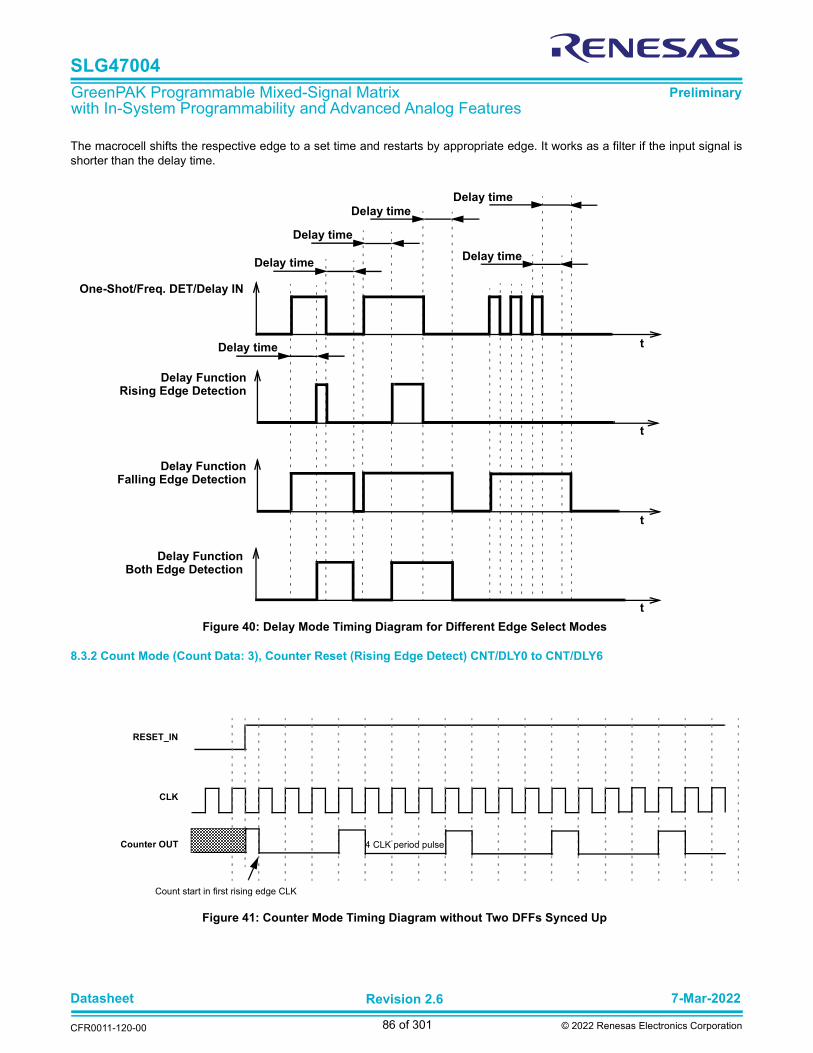
Datasheet 7-Mar-2022
CFR0011-120-00
Revision 2.6
86 of 301 © 2022 Renesas Electronics Corporation
SLG47004
GreenPAK Programmable Mixed-Signal Matrix with In-System Programmability and Advanced Analog Features
Preliminary
The macrocell shifts the respective edge to a set time and restarts by appropriate edge. It works as a filter if the input signal isshorter than the delay time.
8.3.2 Count Mode (Count Data: 3), Counter Reset (Rising Edge Detect) CNT/DLY0 to CNT/DLY6
Figure 40: Delay Mode Timing Diagram for Different Edge Select Modes
Figure 41: Counter Mode Timing Diagram without Two DFFs Synced Up
One-Shot/Freq. DET/Delay IN
Delay FunctionRising Edge Detection
Delay FunctionFalling Edge Detection
Delay FunctionBoth Edge Detection
t
t
t
t
Delay time
Delay time
Delay time
Delay time
Delay time
Delay time
RESET_IN
CLK
Counter OUT
Count start in first rising edge CLK
4 CLK period pulse

Datasheet 7-Mar-2022
CFR0011-120-00
Revision 2.6
87 of 301 © 2022 Renesas Electronics Corporation
SLG47004
GreenPAK Programmable Mixed-Signal Matrix with In-System Programmability and Advanced Analog Features
Preliminary
Figure 42: Counter Mode Timing Diagram with Two DFFs Synced Up
RESET_IN
CLK
Counter OUT
Count start in 0 CLK after reset
4 CLK period pulse

Datasheet 7-Mar-2022
CFR0011-120-00
Revision 2.6
88 of 301 © 2022 Renesas Electronics Corporation
SLG47004
GreenPAK Programmable Mixed-Signal Matrix with In-System Programmability and Advanced Analog Features
Preliminary
8.3.3 One-Shot Mode CNT/DLY0 to CNT/DLY6
This macrocell will generate a pulse whenever a selected edge is detected on its input. Register bits set the edge selection. Thepulse width is determined by counter data and clock selection properties.
The output pulse polarity (non-inverted or inverted) is selected by register bit. Any incoming edges will be ignored during the pulsewidth generation. The following diagram shows one-shot function for non-inverted output.
This macrocell generates a high level pulse with a set width (defined by counter data) when detecting the respective edge. It doesnot restart while pulse is high.
8.3.4 Frequency Detection Mode CNT/DLY0 to CNT/DLY6
Rising Edge: The output goes high if the time between two successive edges is less than the delay. The output goes low if thesecond rising edge has not come after the last rising edge in specified time.
Falling Edge: The output goes high if the time between two falling edges is less than the set time. The output goes low if thesecond falling edge has not come after the last falling edge in specified time.
Both Edge: The output goes high if the time between the rising and falling edges is less than the set time, which is equivalent tothe length of the pulse. The output goes low if after the last rising/falling edge and specified time, the second edge has not come.
Figure 43: One-Shot Function Timing Diagram
One-Shot/Freq. DET/Delay IN
One-Shot FunctionRising Edge Detection
One-Shot FunctionFalling Edge Detection
One-Shot FunctionBoth Edge Detection
t
t
t
t
Delay time
Delay time
Delay time
Delay time
Delay time
Delay time
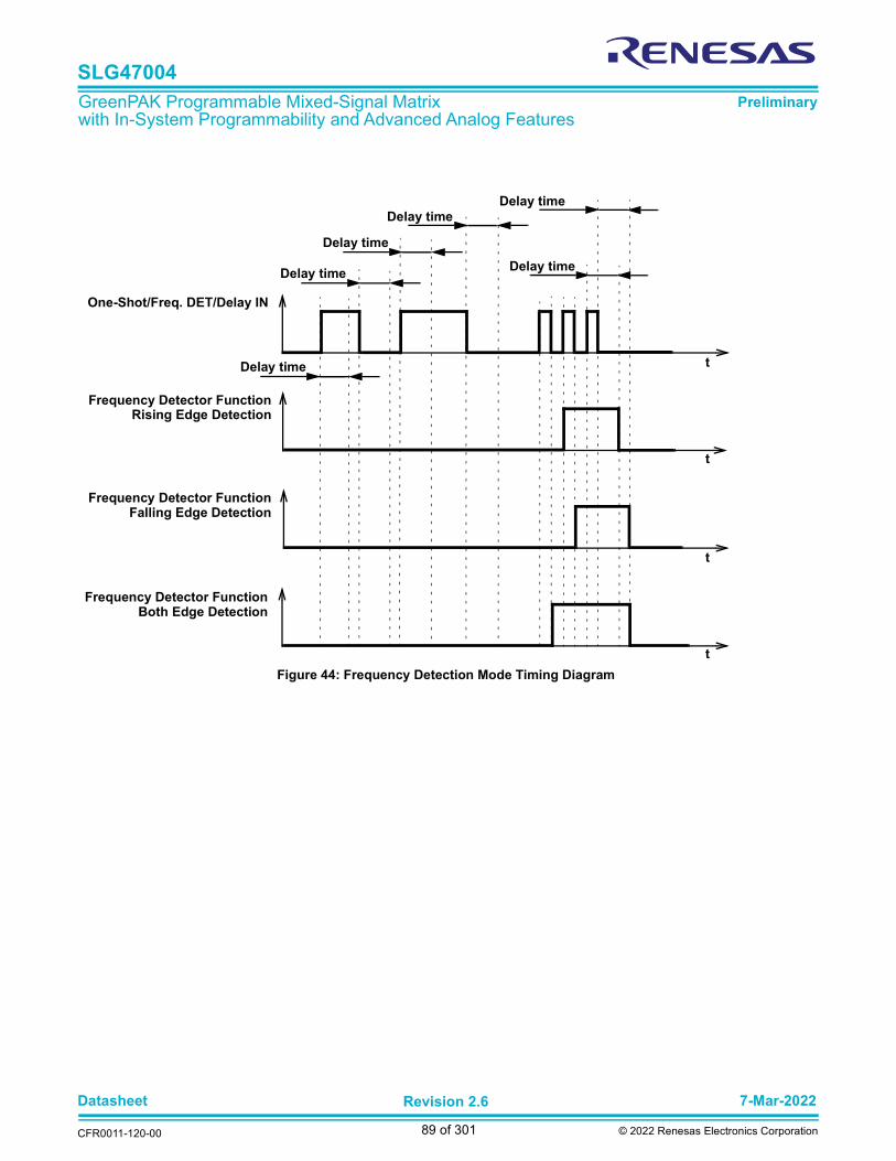
Datasheet 7-Mar-2022
CFR0011-120-00
Revision 2.6
89 of 301 © 2022 Renesas Electronics Corporation
SLG47004
GreenPAK Programmable Mixed-Signal Matrix with In-System Programmability and Advanced Analog Features
Preliminary
Figure 44: Frequency Detection Mode Timing Diagram
One-Shot/Freq. DET/Delay IN
Frequency Detector FunctionRising Edge Detection
Frequency Detector FunctionFalling Edge Detection
Frequency Detector FunctionBoth Edge Detection
t
t
t
t
Delay time
Delay time
Delay time
Delay time
Delay time
Delay time
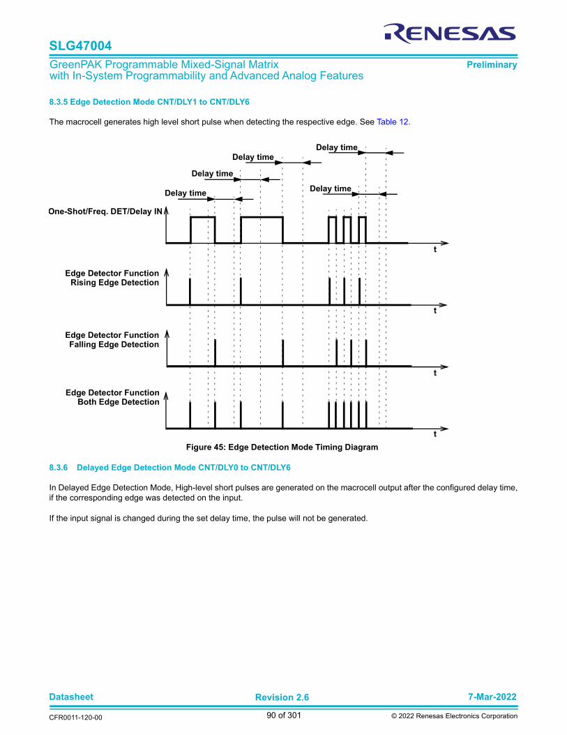
Datasheet 7-Mar-2022
CFR0011-120-00
Revision 2.6
90 of 301 © 2022 Renesas Electronics Corporation
SLG47004
GreenPAK Programmable Mixed-Signal Matrix with In-System Programmability and Advanced Analog Features
Preliminary
8.3.5 Edge Detection Mode CNT/DLY1 to CNT/DLY6
The macrocell generates high level short pulse when detecting the respective edge. See Table 12.
8.3.6 Delayed Edge Detection Mode CNT/DLY0 to CNT/DLY6
In Delayed Edge Detection Mode, High-level short pulses are generated on the macrocell output after the configured delay time,if the corresponding edge was detected on the input.
If the input signal is changed during the set delay time, the pulse will not be generated.
Figure 45: Edge Detection Mode Timing Diagram
One-Shot/Freq. DET/Delay IN
Edge Detector FunctionRising Edge Detection
Edge Detector FunctionFalling Edge Detection
Edge Detector FunctionBoth Edge Detection
t
t
t
t
Delay time
Delay time
Delay time
Delay time
Delay time

Datasheet 7-Mar-2022
CFR0011-120-00
Revision 2.6
91 of 301 © 2022 Renesas Electronics Corporation
SLG47004
GreenPAK Programmable Mixed-Signal Matrix with In-System Programmability and Advanced Analog Features
Preliminary
8.3.7 CNT/FSM Mode CNT/DLY0
Figure 46: Delayed Edge Detection Mode Timing Diagram
Figure 47: CNT/FSM Timing Diagram (Reset Rising Edge Mode, Oscillator is Forced On, UP = 0) for Counter Data = 3
One-Shot/Freq. DET/Delay IN
Delayed Edge DetectorFunction RisingEdge Detection
Delayed Edge DetectorFunction FallingEdge Detection
Delayed Edge DetectorFunction Both
Edge Detection
t
t
t
t
Delay time
Delay time
Delay time
Delay time
Delay time
RESET IN
CLK
3 1 3 2 1 0Q
COUNT END
3 2 1 00
KEEP
2 3 2 1 0
Note: Q = current counter value

Datasheet 7-Mar-2022
CFR0011-120-00
Revision 2.6
92 of 301 © 2022 Renesas Electronics Corporation
SLG47004
GreenPAK Programmable Mixed-Signal Matrix with In-System Programmability and Advanced Analog Features
Preliminary
Figure 48: CNT/FSM Timing Diagram (Set Rising Edge Mode, Oscillator is Forced On, UP = 0) for Counter Data = 3
Figure 49: CNT/FSM Timing Diagram (Reset Rising Edge Mode, Oscillator is Forced On, UP = 1) for Counter Data = 3
SET IN
CLK
3 1 2 1 0 3Q
COUNT END
2 1 0 33
KEEP
2 2 1 0 3
Note: Q = current counter value
RESETI N
CLK
3 5 1 2 3 4Q
COUNT END
5 6 7 80
KEEP
4 9 65533 65534 3 4 5
Note: Q = current counter value
65535

Datasheet 7-Mar-2022
CFR0011-120-00
Revision 2.6
93 of 301 © 2022 Renesas Electronics Corporation
SLG47004
GreenPAK Programmable Mixed-Signal Matrix with In-System Programmability and Advanced Analog Features
Preliminary
8.3.8 Difference in Counter Value for Counter, Delay, One-Shot, and Frequency Detect Modes
There is a difference in counter value for Counter and Delay/One-Shot/Frequency Detect modes. Compared to Counter mode,in Delay/One-Shot/Frequency Detect modes the counter value is shifted for two rising edges of the clock signal. See Figure 51.
Figure 50: CNT/FSM Timing Diagram (Set Rising Edge Mode, Oscillator is Forced On, UP = 1) for Counter Data = 3
Figure 51: Counter Value, Counter Data = 3
SET IN
CLK
3 5 4 5 6 7Q
COUNT END
8 9 10 113
KEEP
4 12 65533 65534 65535 3 4 5
Note: Q = current counter value
One-Shot/Freq. SET/Delay IN
CLK
CNT Out
Delay Data
One-Shot Out
One-Shot Data
DLY Out
CNT Data 0 3 2 1 0 3 2
3 3 3 2 1 3 3
3 3 3 2 1 3 3

Datasheet 7-Mar-2022
CFR0011-120-00
Revision 2.6
94 of 301 © 2022 Renesas Electronics Corporation
SLG47004
GreenPAK Programmable Mixed-Signal Matrix with In-System Programmability and Advanced Analog Features
Preliminary
8.4 WAKE AND SLEEP CONTROLLER
The SLG47004 has a Wake and Sleep (WS) function for ACMP. The macrocell CNT/DLY0 can be reconfigured for this purposeregisters [1224:1223] = 11 and register [1232] = 1. The WS serves for power saving, it allows to switch on and off selected ACMPson selected bit of 16-bit counter.
Note 1: BG/Analog_Good time is long and should be considered in the wake and sleep timing in case it dynamically powers on/off.
Note 2: Wake time should be long enough to make sure ACMP and Vref have enough time to get a sample before going to sleep.
Figure 52: Wake and Sleep Controller
OSC0
CK_OSC Divider
cnt_end
Power Control
From Connection Matrix Output [91] for 2 kHz OSC0.
Analog Control Block
registers [1230:1227]
WS_PD to WS out state selection register [1233]
WS clock freq. selection
registers [1383:1368]WS ratio control data
registers [633], [611]
WS mode: normal or short wake
ACMPs_PD
WS_out
bg/regulator pd
ACMP0, ACMP1 OUT
To Connection Matrix Input[57:56]
From Connection Matrix Output [90:89]
WS_out
Note: WS_PD is High at OSC0 power-down
WS Controller
CNT0_outTo Connection Matrix Input [12]
ck
CNT
2ACMPs_PD
+-
ACMPs WS EN [1:0] register [612], register [634]
01
BG/Analog_Good
ACMPs
2
2
WS_PD(from OSC PD)
WS_PD
2
WS_out

Datasheet 7-Mar-2022
CFR0011-120-00
Revision 2.6
95 of 301 © 2022 Renesas Electronics Corporation
SLG47004
GreenPAK Programmable Mixed-Signal Matrix with In-System Programmability and Advanced Analog Features
Preliminary
Figure 53: Wake and Sleep Timing Diagram, Normal Wake Mode, Counter Reset is Used
Figure 54: Wake and Sleep Timing Diagram, Short Wake Mode, Counter Reset is Used
Normal ACMP Operation
ACMP follows input
Sleep Mode ACMP Latches New Data
Data is latched
Normal ACMP Operation
ACMP follows input
Force Wake
BG/AnalogStartup time*
Sleep ModeACMP Latches Last Data
BG/AnalogStartup time*
BG/Analog_Good(internal signal)
ACMP_PD is High (From Connection Matrix)
CNT_RST(From Connection Matrix)
CNT0_out (To Connection Matrix)
time between Reset goes low and 1st WS clock rising edge
WS_out(internal signal)
Note: CNT0_out is a delayed WS_out signal for 1us to make sure the data is correct during LATCH.
Sleep ModeACMP Latches
New Data
CNT0_out (To Connection Matrix)
Sleep Mode ACMP Latches New Data
BG/Analog_Good(internal signal)
ACMP_PD is High(From Connection Matrix)
Data is latched
BG/AnalogStartup time*
CNT_RST(From Connection Matrix)
Sleep ModeACMP Latches
New Data Normal ACMP Operation for short time
ACMP follows input
Normal ACMP Operation for short time
ACMP follows input
Data is latched
Force Wake
Sleep ModeACMP Latches Last Data
BG/AnalogStartup time*
time between Reset goes low and 1st WS clock rising edge
WS_out(internal signal)
Note: CNT0_out is a delayed WS_out signal for 1us to make sure the data is correct during LATCH.

Datasheet 7-Mar-2022
CFR0011-120-00
Revision 2.6
96 of 301 © 2022 Renesas Electronics Corporation
SLG47004
GreenPAK Programmable Mixed-Signal Matrix with In-System Programmability and Advanced Analog Features
Preliminary
Note: If low power BG is powered on/off by WS, the wake time should be longer than 2.1 ms. The BG/analog start up time willtake maximal 2 ms. If low power BG is always on, OSC0 period is longer than required wake time. The short wake mode can beused to reduce the current consumption. The short wake mode is edge triggered, when the wake signal is latched by rising edgeand released the Power-On signal after the ACMP output data is latched. This allows to have a valid ACMP data for any type ofwake signal and have the optimized current consumption.
Figure 55: Wake and Sleep Timing Diagram, Normal Wake Mode, Counter Set is Used
Figure 56: Wake and Sleep Timing Diagram, Short Wake Mode, Counter Set is Used
Normal ACMP Operation
ACMP follows input
Sleep Mode ACMP Latches New Data
Data is latched
BG/AnalogStartup time*
Force Sleep
Sleep ModeACMP Latches Last Data
BG/Analog_Good(internal signal)
ACMP_PD is High(From Connection Matrix)
CNT_SET(From Connection Matrix)
CNT0_out (To Connection Matrix)
time between Reset goes low and 1st WS clock rising edge
WS_out(internal signal)
Note: CNT0_out is a delayed WS_out signal for 1 us to make sure the data is correct during LATCH.
Sleep Mode ACMP Latches New Data
Data is latched
BG/AnalogStartup time*
Normal ACMP Operation for short time
ACMP follows input
Force Sleep
Sleep ModeACMP Latches Last Data
BG/Analog_Good(internal signal)
ACMP_PD is High (From Connection Matrix)
CNT_RST(From Connection Matrix)
CNT0_out (To Connection Matrix)
time between Reset goes low and 1st WS clock rising edge
WS_out(internal signal)
Note: CNT0_out is a delayed WS_out signal for 1us to make sure the data is correct during LATCH.
Datasheet 7-Mar-2022
CFR0011-120-00
Revision 2.6
97 of 301 © 2022 Renesas Electronics Corporation
SLG47004
GreenPAK Programmable Mixed-Signal Matrix with In-System Programmability and Advanced Analog Features
Preliminary
To use any ACMP under WS controller, the following settings must be done:
CNT/DLY0 must be set to Wake and Sleep Controller function (for all ACMPs); Register WS => enable (for each ACMP separately); CNT/DLY0 set/reset input = 0 (for all ACMPs).
As the OSC any oscillator with any pre-divider can be used. The user can select a period of time while the ACMP is sleeping ina range of 1 - 65535 clock cycles. Before they are sent to sleep their outputs are latched, so the ACMPs remain their state (Highor Low) while sleeping.
WS controller has the following settings:
Wake and Sleep Output State (High/Low) If OSC is powered off (Power-down option is selected; Power-down input = 1) and Wake and Sleep Output State = High, theACMP is continuously on.If OSC is powered off (Power-down option is selected; Power-down input = 1) and Wake and Sleep Output State = Low, theACMP is continuously off.Both cases WS function is turned off.
Counter Data (Range: 1 to 65535) User can select wake and sleep ratio of the ACMP; counter data = sleep time, one clock = wake time.
Q mode - defines the state of WS counter data when Set/Reset signal appears Reset - when active signal appears, the WS counter will reset to zero and High level signal on its output will turn on the ACMPs. When Reset signal goes out, the WS counter will go Low and turn off the ACMPs until the counter counts up to the end. Set - when active signal appears, the WS counter will stop and Low level signal on its output will turn off the ACMPs. When Set signal goes out, the WS counter will go on counting and High level signal will turn on the ACMPs while counter is counting up to the end.
Note: The OSC0 matrix power down to control ACMP WS is not supported for short wait time option.
Edge Select defines the edge for Q modeHigh level Set/Reset - switches mode Set/Reset when level is High
Note: Q mode operates only in case of "High Level Set/Reset”.
Wake time selection - time required for wake signal to turn the ACMPs on
Normal Wake Time - when WS signal is High, it takes BG/analog start up time to turn the ACMPs on. They will stay on until WS signal is Low again. Wake time is one clock period. It should be longer than BG turn on time and minimal required comparing time of the ACMP.
Short Wake Time - when WS signal is High, it takes BG/analog start up time to turn the ACMPs on. They will stay on for 1 µs and turn off regardless of WS signal. The WS signal width does not matter.
Keep - pauses counting while Keep = 1 Up - reverses counting
If Up = 1, CNT is counting up from user selected value to 65535.
If Up = 0, CNT is counting down from user selected value to 0.

Datasheet 7-Mar-2022
CFR0011-120-00
Revision 2.6
98 of 301 © 2022 Renesas Electronics Corporation
SLG47004
GreenPAK Programmable Mixed-Signal Matrix with In-System Programmability and Advanced Analog Features
Preliminary
9 Analog Comparators
9.1 ANALOG COMPARATORS OVERVIEW
There are two Low Power Rail-to-Rail General Purpose Analog Comparators (ACMP) macrocells in the SLG47004. For theACMP macrocells to be used in a GreenPAK design, the power-up signals (ACMP0_L_pdb and ACMP1_L_pdb) need to beactive. By connecting to signals coming from the Connection Matrix, it is possible to have each ACMP be ON continuously, OFFcontinuously, or switched on periodically, based on a digital signal coming from the Connection Matrix. When ACMP is powereddown, its output is low. Two General Purpose Analog Comparators are optimized for low power operation.
Each of the General Purpose ACMP cells has a positive input signal that can be provided by a variety of external sources, andcan also have a selectable gain stage (1x, 0.5x, 0.33x, 0.25x) before connection to the analog comparator. The gain divider isunbuffered and has an input resistance of 2 MΩ (typ) for 0.5x, 0.33x, 0.25x, and 10 GΩ for 1x. Each of the General PurposeACMP macrocells has a negative input signal that is either created from an internal Vref or provided by any external source(from external pins). Note that the external Vref signal is filtered with a 2nd order low pass filter with 8 kHz typical bandwidth, seein Figure 57 and Figure 58.
Input bias current < 1 nA (typ).
PWR UP = 1 => ACMP is powered up.
PWR UP = 0 => ACMP is powered down.
Both General Purpose Analog Comparators have "Low Energy Power Up" setting (register [608] - AСMP0, register [630] -AСMP1). When enabled, it allows reducing average power consumption during ACMP power up process. This setting changespower up sequence of analog macrocells:
Low Energy Power Up register [608], register [630] = 0 - all analog macrocells associated with ACMP turns on simultaneously.
Low Energy Power Up register [608], register [630] = 1 - the first macrocell that begins to turn on is Bandgap. Other analogmacrocells begin to turn on only after BG_OK signal is valid. This option slightly increases general ACMP Power-On time, whilereducing the average current consumption.
During power-up, the ACMP output will remain LOW, and then becomes valid after power up signal goes high for ACMP0_L andACMP1_L (see parameter tstart in Table 18).
Each cell also has a flexible hysteresis selection, to offer hysteresis of 32 steps, but not more than Vref voltage. It means thatthere are 6-bits to select Vref and independent 6-bits to select the hysteresis (no need to have an adder logic).
It’s possible to enable low pass filter at the Vref input. But it’s highly recommended to enable this LPF only when hysteresisVhys > 196 mV.
ACMP0_L IN+ options are OA0_out, GPIOx (PIN), VDD.
ACMP1_L IN+ options are OA1, GPIOx (PIN), ACMP0L_IN+, Temp Sensor OUT.
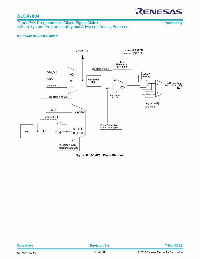
Datasheet 7-Mar-2022
CFR0011-120-00
Revision 2.6
99 of 301 © 2022 Renesas Electronics Corporation
SLG47004
GreenPAK Programmable Mixed-Signal Matrix with In-System Programmability and Advanced Analog Features
Preliminary
9.1.1 ACMP0L Block Diagram
Figure 57: ACMP0L Block Diagram
1000000
0111111-
0000000Vref
GPIO
00
01
10
GPIO
Internal VDD
SelectableGain
registers [615:614]
to ACMP1_L
Vref
+
-
From Connection Matrix Output [89]
pUp
6-bitHysteresisSelection
registers [629:624]
registers [617:616]Low Power
ACMP
To Connection Matrix Input [56]
ACMPReady
Latch
0
1
register [612]
W/S Control
OA0_Out
registers [623:618]
registers [629:624]registers [623:618]
LPF
register [613]
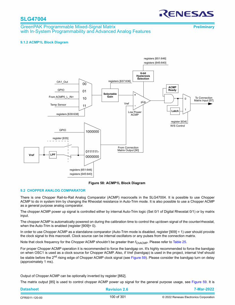
Datasheet 7-Mar-2022
CFR0011-120-00
Revision 2.6
100 of 301 © 2022 Renesas Electronics Corporation
SLG47004
GreenPAK Programmable Mixed-Signal Matrix with In-System Programmability and Advanced Analog Features
Preliminary
9.1.2 ACMP1L Block Diagram
9.2 CHOPPER ANALOG COMPARATOR
There is one Chopper Rail-to-Rail Analog Comparator (ACMP) macrocells in the SLG47004. It is possible to use ChopperACMP to do in system trim by changing the Rheostat resistance in Auto-Trim mode. It is also possible to use a Chopper ACMPas a general purpose analog comparator.
The chopper ACMP power up signal is controlled either by internal Auto-Trim logic (Set 0/1 of Digital Rheostat 0/1) or by matrixinput.
The chopper ACMP is automatically powered on during the calibration time to control the up/down signal of the counter/rheostat,when the Auto-Trim is enabled (register [909]= 0).
In order to use Chopper ACMP as a standalone comparator (Auto-Trim mode is disabled, register [909] = 1) user should providethe clock signal to this macrocell. Clock source can be internal oscillators or any pulses from the connection matrix.
Note that clock frequency for the Chopper ACMP shouldn’t be greater than fChACMP. Please refer to Table 25.
For proper Chopper ACMP operation it is recommended to force the bandgap on. It's highly recommended to force the bandgapon when OSC1 is used as a clock source for Chopper ACMP. Also, if Vref (bandgap) is used in the project, internal Vref should
be stable before the 2nd rising edge of Chopper ACMP clock signal (see Figure 59). Please consider the bandgap turn on delay(approximately 1 ms).
Output of Chopper ACMP can be optionally inverted by register [882].
The matrix output [85] is used to control chopper ACMP power up signal for the general purpose usage, see Figure 59. It is
Figure 58: ACMP1L Block Diagram
1000000
0111111-
0000000
GPIO
00
01
10
11
From ACMP0_L_IN+
Temp Sensor
SelectableGain
registers [637:636]
Vref
+
-
From Connection Matrix Output [90]
pUp
6-bitHysteresisSelection
registers [651:646]
registers [639:638]Low Power
ACMP
To Connection Matrix Input [57]
ACMPReady
Latch
0
1
register [634]
W/S Control
GPIO
OA1_Out
registers [645:640]
registers [651:646]
registers [645:640]
Vref LPF
register [635]

Datasheet 7-Mar-2022
CFR0011-120-00
Revision 2.6
101 of 301 © 2022 Renesas Electronics Corporation
SLG47004
GreenPAK Programmable Mixed-Signal Matrix with In-System Programmability and Advanced Analog Features
Preliminary
possible to use the chopper ACMP as a general purpose ACMP after Auto-Trim procedure is completed, since the power upsignal is a logic OR of the latched Set (Digital Rheostat 0/1) signal and matrix signal. If Auto-Trim (Set 0/1 of Digital Rheostat0/1) is disabled and chopper ACMP channel is set to Auto (Channel 0/1), then ACMP output defaults to Channel 0 whileChannel 1 is ignored.
The power-up signals need to be active high in order to use the Chopper ACMP. By connecting to signals coming from theConnection Matrix, it is possible to have ACMP be ON continuously, OFF continuously, or switched on periodically based on adigital signal coming from the Connection Matrix. When ACMP is powered down, its output is low.
There are no Gain and Hysteresis selection for chopper ACMP compared to the ACMP0L and ACMP1L.
It's possible to select different reference sources for Chopper ACMP. It can be:
external voltage from pin; divided internal voltage from internal reference source (from 32 mV to 2048 mV); divided internal reference voltage from HD Buffer (64 steps); divided VDDA voltage (64 steps). For more information see Section 15.
The positive input of the Chopper ACMP can be connected to the Op Amp0 out or Op Amp1 out or In Amp out, or to the externalPIN.
The inputs of Chopper ACMP can be reconfigured while operating in AutoTrim mode. There is one configuration of inputs(Figure 59) for case when Set0 (Digital Rheostat 0) signal is latched, and another configuration of Chopper ACMP inputs whenSet1 (Digital Rheostat 1) signal is latched. For example, M1 MUX can be configured to operate with In Amp out when Set0(Digital Rheostat 0) is latched and Chopper_ACMP+ pin when Set1 (Digital Rheostat 1) is latched. The same way, “-” input ofChopper ACMP can be configured to work with any of possible inputs when Set0 (Digital Rheostat 0) or Set1 (Digital Rheostat1) are latched.
Note that the default configuration is the configuration for Set0 (Digital Rheostat 0) signal. When Chopper ACMP operates asseparate ACMP and AutoTrim function is disabled, inputs of Chopper ACMP are defined by registers [893:892].
Note that Chopper ACMP will automatically enable HD Buffer if HD Buffer is selected as a source for Chopper ACMP In-signal(register 946 = 0) and Chopper ACMP is powered up.

Datasheet 7-Mar-2022
CFR0011-120-00
Revision 2.6
102 of 301 © 2022 Renesas Electronics Corporation
SLG47004
GreenPAK Programmable Mixed-Signal Matrix with In-System Programmability and Advanced Analog Features
Preliminary
9.3 ACMP SAMPLING MODE
Both General Purpose Analog Comparators (ACMPL0 and ACMPL1) have an optional sampling mode. In this mode, ACMP isenabled for the shortest amount of time after rising edge at Power Up input to get a valid data. Then ACMP latches its value andgoes sleep again.
Registers [610], [632] enable sampling mode for two comparators.
Figure 59: Chopper ACMP Block Diagram
Matrixinput [55]
from OpAmp1 out
from OpAmp0 out
Trim_ACMP+
M1
PIN
Pwr_Up
Matrix output [85]
register [882]
from InAmp out
ORfrom Autotrim
logic of RH0
from Autotrimlogic of RH1
registers [873:872]
2 bit 2 bit
0default value
from Autotrim logic
0000000
0000001
0111110
0111111
registers [765:760]
HD Buf
6-b
it d
ivid
er0
1
register [780]
VddA
1/64
2/64
63/64
64/64
0
1
register [660]
from matrix
output [94]
register [661]
Bandgap
Vref
PwrUp
2.048V
AM0
DM0
AM1
PwrUp0 1
"ChopACMP-" reference
"ChopACMP+" reference
000000
000001
111110
111111
6-b
it d
ivid
er
1/64
2/64
63/64
1/64
0
1
6
7
7
registers [934:928]
7 bit
7 bit
AM2
DM1
AM3
000001
111110
111111
6-b
it d
ivid
er
2/64
63/64
64/64
7
6
[6]
0
default value
from Autotrim logic
64/64
000000
registers [875:874]
registers [941:936]
0
1register [766]
Matrix
output [99]
registers [782]
0
1
ext. Vref
AM4
register [946]
0
1
AM5
defined by
registers [934] and [942]
Matrix output [75]
from
Clk
M_
CK
0
...OSC0
dividers
Registers [899:895]
Matrix output [80]
from
Clk
M_
CK
1
Registers [894,907:904]
...OSC0
dividers
Chopper
ACMP
+
-
Clk0
Clk1

Datasheet 7-Mar-2022
CFR0011-120-00
Revision 2.6
103 of 301 © 2022 Renesas Electronics Corporation
SLG47004
GreenPAK Programmable Mixed-Signal Matrix with In-System Programmability and Advanced Analog Features
Preliminary
9.4 ACMP TYPICAL PERFORMANCE
Figure 60: Propagation Delay vs. Vref for ACMPx at T = 25 °C, VDD = 2.4 V to 5.5 V, Hysteresis = 0
Figure 61: ACMPx Power-On Delay vs. VDD at BG - Forced
0
2
4
6
8
10
12
0 512 1024 1536 2048
Pro
pa
ga
tio
n D
ela
y (
μs)
Vref (mV)
High To Low, Overdrive = 10 mV
Low to High, Overdrive = 10 mV
High to Low, Overdrive = 100 mV
Low to High, Overdrive = 100 mV
70
90
110
130
150
170
190
2.4 2.7 3.0 3.3 3.6 3.9 4.2 4.5 4.8 5.1 5.4
Po
we
r-O
n D
ela
y (
μs)
VDD (V)
ACMPx (T = -40°C)
ACMPx (T = 25°C)
ACMPx (T = 85°C)

Datasheet 7-Mar-2022
CFR0011-120-00
Revision 2.6
104 of 301 © 2022 Renesas Electronics Corporation
SLG47004
GreenPAK Programmable Mixed-Signal Matrix with In-System Programmability and Advanced Analog Features
Preliminary
Figure 62: ACMPx Input Offset Voltage vs. Vref at T = -40 °C to 85 °C, VDD = 2.4 V to 5.5 V, Gain = 1
Figure 63: Chopper ACMP Input Offset Voltage vs. Vref at T = -40 °C to 85 °C, VDD = 2.4 V to 5.5 V, Gain = 1
-8
-6
-4
-2
0
2
4
6
32 480 1024 1600 2048
VO
FF
SE
T(m
V)
Vref (mV)
-250
-200
-150
-100
-50
0
50
100
150
200
250
300
350
400
450
500
32 480 1024 1600 2048
VO
FF
SE
T(μ
V)
Vref (mV)

Datasheet 7-Mar-2022
CFR0011-120-00
Revision 2.6
105 of 301 © 2022 Renesas Electronics Corporation
SLG47004
GreenPAK Programmable Mixed-Signal Matrix with In-System Programmability and Advanced Analog Features
Preliminary
Figure 64: ACMPx Current Consumption vs. VDD
Figure 65: Chopper ACMP Current Consumption vs. VDD (with 2.048 kHz Clock)
5
5.5
6
6.5
7
7.5
8
2.5 3 3.5 4 4.5 5 5.5
I DD
(μA
)
VDD (V)
T = 85 °C
T = 25 °C
T = -40 °C
25
30
35
40
45
50
2.5 3 3.5 4 4.5 5 5.5
I DD
(μA
)
VDD (V)
T = 85 °C
T = 25 °C
T = -40 °C

Datasheet 7-Mar-2022
CFR0011-120-00
Revision 2.6
106 of 301 © 2022 Renesas Electronics Corporation
SLG47004
GreenPAK Programmable Mixed-Signal Matrix with In-System Programmability and Advanced Analog Features
Preliminary
10 Programmable Operational Amplifiers
10.1 GENERAL DESCRIPTION
The SLG47004 contains three operational amplifiers with rail-to-rail input and output. Two of them (Programmable Op Amps)have the additional functions of driving internal analog FETs (Voltage Regulator and Current Sink modes) and Comparatormode. The third Internal Op Amp is an amplifier with internal resistors, and can be configured as a difference amplifier with Gain= 1. All three op amps can function as instrumentation amplifiers. The structures of the op amps are shown in Figure 66 andFigure 67.
Figure 66: Programmable Operational Amplifier OA0, OA1 Internal Circuit

Datasheet 7-Mar-2022
CFR0011-120-00
Revision 2.6
107 of 301 © 2022 Renesas Electronics Corporation
SLG47004
GreenPAK Programmable Mixed-Signal Matrix with In-System Programmability and Advanced Analog Features
Preliminary
Each of the two Programmable Op Amp inputs has a hardware connection to the external pin and an optional connection to theinternal voltage reference source, which makes it possible to create precise voltage or current source. For more detaileddescription of op amp Vref sources see Section 15. The output of the operational amplifier is hardwired to an external pin. Thisoutput can also be connected to the Programmable Trim block of rheostat macrocell, ACMP non-inverting input (ACMP0_L+ forOA0, ACMP1_L+ for OA1), or control the corresponding Analog Switch, depending on the mode of operation. EachProgrammable Op Amp can also be configured as an analog comparator, in which case its output signal is connected to theConnection Matrix through a dedicated buffer.
Each Programmable Op Amp has a programmable bandwidth that can be set by two register bits. In addition, internal chargepump setting for each Op Amp must be changed according to bandwidth selection, see Table 56.
Internal charge pump can be disabled if input common-mode voltage VCM < (VDDA - 1.5 V). But it is strongly recommended tokeep the default setting (enable charge pump).
The bandwidths may vary up to +/-30 % over PVT. Each operational amplifier is factory trimmed. This trimming is independent ofthe trimming associated with the onboard digital rheostat (system calibration).
The Internal operational amplifier shares its inputs with the Programmable Op Amps outputs. The voltage reference for theinternal amplifier can be sourced from either the internal or external Vref. Note that if the internal Vref is used as a source for theinstrumentation amplifier Vref, the user can optionally connect this Vref to the output pin, or disconnect the Vref from output pinand use this pin as GPIO.
Also, if the Internal Op Amp is inactive (In Amp Mode is disabled), the user can use the In Amp_Vref pin as GPIO. The InAmp_Out pin can be configured as GPI.
Figure 67: Internal Operational Amplifier Circuit
Table 56: Op Amp Bandwidth Settings
Op Amp Bandwidth Selection
Op Amp0 Op Amp1 Op Amp2 (Internal)
Bandwidth Selection
Charge Pump Frequency
Bandwidth Selection
Charge Pump Frequency
BandwidthSelection
Charge Pump Frequency
Register Bit → 745 744 955 954 747 746 963 962 749 748 971 970
128 kHz 0 0 0 0 0 0 0 0 0 0 0 0
512 kHz 0 1 0 1 0 1 0 1 0 1 0 1
2.048 MHz 1 0 1 0 1 0 1 0 1 0 1 0
8.192 MHz 1 1 1 1 1 1 1 1 1 1 1 1

Datasheet 7-Mar-2022
CFR0011-120-00
Revision 2.6
108 of 301 © 2022 Renesas Electronics Corporation
SLG47004
GreenPAK Programmable Mixed-Signal Matrix with In-System Programmability and Advanced Analog Features
Preliminary
10.2 MODES OF OPERATION
In order to use any of the op amp macrocells in the GreenPAK Designer, the power up signal (PWR_UP) must be set to logicHigh. By default, all op amp macrocells are turned off after SLG47004 startup. During power-up, outputs of all op amps willremain in a Hi-Z state and then become valid (see parameter ton in Table 24).
Operational amplifiers turn-on time can be decreased by setting register bits [759:757] to 1. In this case op amps analogsupporting blocks are always turned on. Note that current consumption of op amp will be increased when op amp is powereddown and bits [759:757] is 1 (see Section 3.13).
See the list below for the op amp operation modes:
Operational Amplifier mode; Instrumentation Amplifier mode; Analog Comparator mode; Voltage Regulator mode; Current Sink mode.
10.2.1 Operational Amplifier Mode
In this mode, the Programmable Op Amp operates as a conventional operational amplifier. Also, the Programmable Op Ampcan source the corresponding non-inverting ACMP input (see ACMP macrocell settings). The output of the Programmable OpAmp macrocell is in a Hi-Z state while the macrocell is turned off.
Figure 68 shows the example of differential amplifier with input offset voltage compensation with help of digital rheostat andprogrammable trim block. Zero input voltage equal to output voltage VOUT = VDD/2.
10.2.2 Instrumentation Amplifier Mode
If this mode is active (Matrix Output [98] is High level), the two Programmable Op Amps and the single Internal Op Amp worktogether in Instrumentation Amplifier configuration, shown in Figure 69. When power up signal is logic LOW the output of In Ampis in Hi-Z state.
Figure 68: Example of Input Offset Voltage Compensation

Datasheet 7-Mar-2022
CFR0011-120-00
Revision 2.6
109 of 301 © 2022 Renesas Electronics Corporation
SLG47004
GreenPAK Programmable Mixed-Signal Matrix with In-System Programmability and Advanced Analog Features
Preliminary
The absolute value of internal resistors R1, R2, R3, R4 is 100 kΩ. The resistors Rf and Rg are user defined external resistors.
The output voltage VOUT of the instrumentation amplifier shown in Figure 69 is
The user can trim both the gain and the offset error of the instrumentation amplifier using two of the Rheostats from theSLG47004. Figure 70 shows the configuration of the instrumentation amplifier in this scenario.
Figure 69: Instrumentation Amplifier Structure
VOUT = (1 + 2Rf / Rg)(VIN+ - VIN-) + VREF

Datasheet 7-Mar-2022
CFR0011-120-00
Revision 2.6
110 of 301 © 2022 Renesas Electronics Corporation
SLG47004
GreenPAK Programmable Mixed-Signal Matrix with In-System Programmability and Advanced Analog Features
Preliminary
Note that in Figure 70, the Demux connects to the Vref external input with an internal buffer (register [756] = 1). This allows us toeliminate the influence of resistor divider Rdiv and Rheostat0 on instrumentation amplifier.
It is possible to use a built-in Auto-Trim function for either setting the zero point of the Wheatstone bridge sensor using the InAmp or tuning a system output voltage to the desired level. However, the following limitations exist for using the built-in Auto-Trim function to trim both total system offset and system gain errors:
- The Auto-Trim procedures of total offset compensation and system gain error must be done iteratively starting and finishingwith the total offset compensation: 1st iteration - offset compensation, 2nd iteration - gain trim, 3rd iteration - offsetcompensation. Extra iterations can be added to achieve a better accuracy. The last iteration should be an offsetcompensation.
- Total system offset (sensor offset + Op Amp1 offset + Op Amp2 offset) must not be greater than Vsensor_output_range/2.
It's possible to power external components like bridge or ADC from internal HD Buffer of SLG47004 to improve accuracy ofsystem.
10.2.3 Analog Comparator Mode
Both operational amplifiers have an Analog Comparator mode in which they work as conventional rail-to-rail comparators.
10.2.4 Voltage Regulator Mode
In this mode, the op amp output drives P-FET (part of Analog Switch). Note that FETs of Analog Switches have differentresistances. Analog Switch 0 has Rds_PMOS << Rds_NMOS, while Analog Switch 1 has Rds_NMOS << Rds_PMOS. That'swhy it is recommended to implement voltage regulator mode using Analog Switch 0. In this mode the op amp output is Highwhen the macrocell is turned off. Figure 71 (A) shows the typical implementation of the voltage source function. Optionally, the
Figure 70: Instrumentation Operational Amplifier Configuration for Users Trim

Datasheet 7-Mar-2022
CFR0011-120-00
Revision 2.6
111 of 301 © 2022 Renesas Electronics Corporation
SLG47004
GreenPAK Programmable Mixed-Signal Matrix with In-System Programmability and Advanced Analog Features
Preliminary
user can use this mode to implement a constant current source with load connected to ground (Figure 71, B, C). Note that opamp must operate in operational amplifier mode (register 750 = 0 for Op Amp0, register 751 = 0 for Op Amp1).
Note that in this mode only an enhanced P channel FET of An_Sw_0 is used.
10.2.5 Current Sink Mode
Also, the op amp output can drive the N-FET (part of the Analog Switch) in order to implement a constant current sink. Note thatFETs of Analog Switches have different resistances. Analog Switch 0 has Rds_PMOS << Rds_NMOS, while Analog Switch 1has Rds_NMOS << Rds_PMOS. That's why it is recommended to implement current sink mode using Analog Switch 1. In thismode, the op amp output is LOW when the macrocell is turned off. Figure 72 (A) shows a typical implementation of this CurrentSink Function. Note that op amp must operate in operational amplifier mode (register 750 = 0 for Op Amp0, register 751 = 0 forOp Amp1).
Figure 71: Typical Implementation of Voltage Regulator (A) and Current Sources (B, C)

Datasheet 7-Mar-2022
CFR0011-120-00
Revision 2.6
112 of 301 © 2022 Renesas Electronics Corporation
SLG47004
GreenPAK Programmable Mixed-Signal Matrix with In-System Programmability and Advanced Analog Features
Preliminary
Note that in this mode only an enhanced N channel FET of An_Sw_1 is used.
10.3 OP AMPS TYPICAL PERFORMANCE
TA = 25 °C, VDDA = 5.0 V, VSS = GND, VCM = VDD/2, VOUT = VDD/2, VL = VDD/2, RL = 1 MΩ to VL, CL = 80 pF, unless otherwisestated.
Figure 72: Constant Current Sink
Figure 73: Op Ampx Input Offset Voltage vs. TA at Input CM Voltage = VDD/2, BW = 128 kHz
0
25
50
75
100
125
150
175
200
225
250
275
-40
-30
-20
-10 0
10
20
30
40
50
60
70
80
Off
set
Vo
lta
ge
(µ
V)
T (°C)
Opampx, 128 kHz, 2.4 V
Opampx, 128 kHz, 5.5 V

Datasheet 7-Mar-2022
CFR0011-120-00
Revision 2.6
113 of 301 © 2022 Renesas Electronics Corporation
SLG47004
GreenPAK Programmable Mixed-Signal Matrix with In-System Programmability and Advanced Analog Features
Preliminary
Figure 74: Op Ampx Input Offset Voltage vs. TA at Input CM Voltage = VDD/2, BW = 512 kHz
Figure 75: Op Ampx Input Offset Voltage vs. TA at Input CM Voltage = VDD/2, BW = 2 MHz
0
25
50
75
100
125
150
175
200
225
250
-40
-30
-20
-10 0
10
20
30
40
50
60
70
80
Off
set
Vo
lta
ge
(µ
V)
T (°C)
Opampx, 512 kHz, 5.5 V
Opampx, 512 kHz, 2.4 V
0
25
50
75
100
125
150
175
200
225
-40
-30
-20
-10 0
10
20
30
40
50
60
70
80
Off
set
Vo
lta
ge
(µ
V)
T (°C)
Opampx, 2 MHz, 5.5 V
Opampx, 2 MHz, 2.4 V
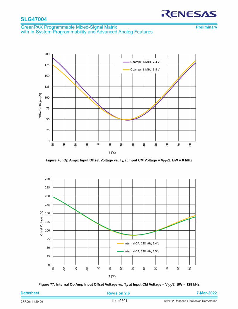
Datasheet 7-Mar-2022
CFR0011-120-00
Revision 2.6
114 of 301 © 2022 Renesas Electronics Corporation
SLG47004
GreenPAK Programmable Mixed-Signal Matrix with In-System Programmability and Advanced Analog Features
Preliminary
Figure 76: Op Ampx Input Offset Voltage vs. TA at Input CM Voltage = VDD/2, BW = 8 MHz
Figure 77: Internal Op Amp Input Offset Voltage vs. TA at Input CM Voltage = VDD/2, BW = 128 kHz
0
25
50
75
100
125
150
175
200-4
0
-30
-20
-10 0
10
20
30
40
50
60
70
80
Off
set
Vo
lta
ge
(µ
V)
T (°C)
Opampx, 8 MHz, 2.4 V
Opampx, 8 MHz, 5.5 V
0
25
50
75
100
125
150
175
200
225
250
-40
-30
-20
-10 0
10
20
30
40
50
60
70
80
Off
set
Vo
lta
ge
(µ
V)
T (°C)
Internal OA, 128 kHz, 2.4 V
Internal OA, 128 kHz, 5.5 V
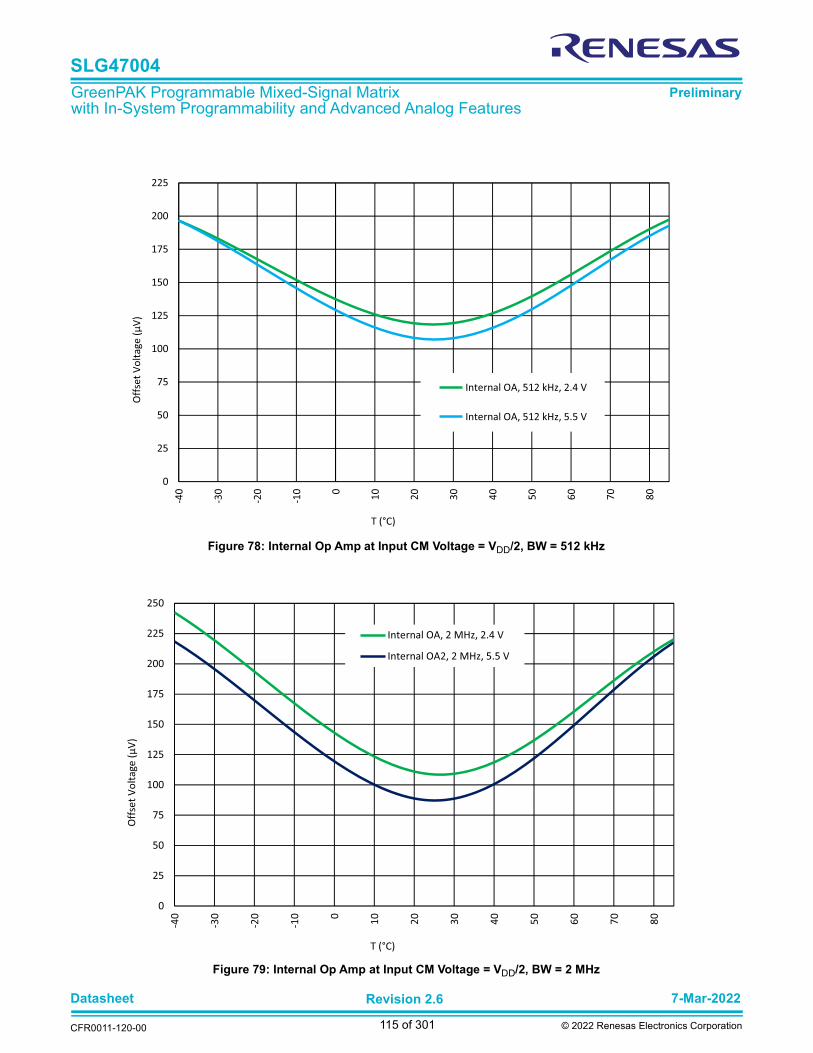
Datasheet 7-Mar-2022
CFR0011-120-00
Revision 2.6
115 of 301 © 2022 Renesas Electronics Corporation
SLG47004
GreenPAK Programmable Mixed-Signal Matrix with In-System Programmability and Advanced Analog Features
Preliminary
Figure 78: Internal Op Amp at Input CM Voltage = VDD/2, BW = 512 kHz
Figure 79: Internal Op Amp at Input CM Voltage = VDD/2, BW = 2 MHz
0
25
50
75
100
125
150
175
200
225-4
0
-30
-20
-10 0
10
20
30
40
50
60
70
80
Off
set
Vo
lta
ge
(µ
V)
T (°C)
Internal OA, 512 kHz, 2.4 V
Internal OA, 512 kHz, 5.5 V
0
25
50
75
100
125
150
175
200
225
250
-40
-30
-20
-10 0
10
20
30
40
50
60
70
80
Off
set
Vo
lta
ge
(µ
V)
T (°C)
Internal OA, 2 MHz, 2.4 V
Internal OA2, 2 MHz, 5.5 V

Datasheet 7-Mar-2022
CFR0011-120-00
Revision 2.6
116 of 301 © 2022 Renesas Electronics Corporation
SLG47004
GreenPAK Programmable Mixed-Signal Matrix with In-System Programmability and Advanced Analog Features
Preliminary
Figure 80: Internal Op Amp Input Offset Voltage vs. TA at Input CM Voltage = VDD/2, BW = 8 MHz
Figure 81: OpAmp0, 1 Input Offset Voltage vs. Input CM Voltage at T = 25 °C, VDDA = 2.4 V
0
25
50
75
100
125
150
175
200-4
0
-30
-20
-10 0
10
20
30
40
50
60
70
80
Off
set
Vo
lta
ge
(µ
V)
T (°C)
Internal OA, 8 MHz, 2.4 V
Internal OA, 8 MHz, 5.5 V
0
10
20
30
40
50
60
70
80
90
100
110
0.0 0.2 0.4 0.6 0.8 1.0 1.2 1.4 1.6 1.8 2.0 2.2 2.4
Inp
ut
Off
set
Vo
lta
ge
(μ
V)
Input CM Voltage (V)
OAx, 128 kHz, 2.4 V
OAx, 512 kHz, 2.4 V
OAx, 2 MHz, 2.4 V
OAx, 8 MHz, 2.4 V

Datasheet 7-Mar-2022
CFR0011-120-00
Revision 2.6
117 of 301 © 2022 Renesas Electronics Corporation
SLG47004
GreenPAK Programmable Mixed-Signal Matrix with In-System Programmability and Advanced Analog Features
Preliminary
Figure 82: OpAmp0, 1 Input Offset Voltage vs. Input CM Voltage at T = 25 °C, VDDA = 5.5 V
Figure 83: Internal OpAmp Input Offset Voltage vs. Input CM Voltage at T = 25 °C, VDDA = 2.4 V
0
10
20
30
40
50
60
70
80
90
100
110
0 0.3 0.6 0.9 1.2 1.5 1.8 2.1 2.4 2.7 3 3.3 3.6 3.9 4.2 4.5 4.8 5.1 5.4
Inp
ut
Off
set
Vo
lta
ge
(μ
V)
Input CM Voltage (V)
OAx, 128 kHz, 5.5 V
OAx, 512 kHz, 5.5 V
OAx, 2 MHz, 5.5 V
OAx, 8 MHz, 5.5 V
0
10
20
30
40
50
60
70
80
90
100
110
120
130
0.0 0.2 0.4 0.6 0.8 1.0 1.2 1.4 1.6 1.8 2.0 2.2 2.4
Inp
ut
Off
set
Vo
lta
ge
(μ
V)
Input CM Voltage (V)
Internal OA, 512 kHz, 2.4 V
Internal OA, 8 MHz, 2.4 V
Internal OA, 2 MHz, 2.4 V
Internal OA, 128 kHz, 2.4 V

Datasheet 7-Mar-2022
CFR0011-120-00
Revision 2.6
118 of 301 © 2022 Renesas Electronics Corporation
SLG47004
GreenPAK Programmable Mixed-Signal Matrix with In-System Programmability and Advanced Analog Features
Preliminary
Figure 84: Internal OpAmp Input Offset Voltage vs. Input CM Voltage at T = 25 °C, VDDA = 5.5 V
Figure 85: Quiescent Current vs. Power Supply Voltage for BW = 128 kHz
0
10
20
30
40
50
60
70
80
90
100
110
120
130
0 0.3 0.6 0.9 1.2 1.5 1.8 2.1 2.4 2.7 3 3.3 3.6 3.9 4.2 4.5 4.8 5.1 5.4
Inp
ut
Off
set
Vo
lta
ge
(μ
V)
Input CM Voltage (V)
Internal OA, 512 kHz, 5.5 V
Internal OA, 8 MHz, 5.5 V
Internal OA, 2 MHz, 5.5 V
Internal OA, 128 kHz, 5.5 V
30
31
32
33
34
35
36
37
38
39
40
2.5 2.8 3.1 3.4 3.7 4 4.3 4.6 4.9 5.2 5.5
Qu
iesc
en
t C
urr
en
t (μ
A)
VDD (V)
T = -40°C
T = 25°C
T = 85°C

Datasheet 7-Mar-2022
CFR0011-120-00
Revision 2.6
119 of 301 © 2022 Renesas Electronics Corporation
SLG47004
GreenPAK Programmable Mixed-Signal Matrix with In-System Programmability and Advanced Analog Features
Preliminary
Figure 86: Quiescent Current vs. Power Supply Voltage for BW = 512 kHz
Figure 87: Quiescent Current vs. Power Supply Voltage for BW = 2 MHz
82
84
86
88
90
92
94
96
2.5 2.8 3.1 3.4 3.7 4 4.3 4.6 4.9 5.2 5.5
Qu
iesc
en
t C
urr
en
t (μ
A)
VDD (V)
T = -40°C
T = 25°C
T = 85°C
226
228
230
232
234
236
238
240
242
244
246
2.5 2.8 3.1 3.4 3.7 4 4.3 4.6 4.9 5.2 5.5
Qu
iesc
en
t C
urr
en
t (μ
A)
VDD (V)
T = -40°C
T = 25°C
T = 85°C

Datasheet 7-Mar-2022
CFR0011-120-00
Revision 2.6
120 of 301 © 2022 Renesas Electronics Corporation
SLG47004
GreenPAK Programmable Mixed-Signal Matrix with In-System Programmability and Advanced Analog Features
Preliminary
Figure 88: Quiescent Current vs. Power Supply Voltage or BW = 8 MHz
Figure 89: OA0 Open Loop Gain and Phase vs. Frequency for BW = 128 kHz
570
580
590
600
610
620
630
640
650
2.5 2.8 3.1 3.4 3.7 4 4.3 4.6 4.9 5.2 5.5
Qu
iesc
en
t C
urr
en
t (μ
A)
VDD (V)
T = -40°C
T = 25°C
T = 85°C
-200
-150
-100
-50
0
50
100
150
200
-40
-30
-20
-10
0
10
20
30
40
50
60
70
80
90
100
110
120
130
140
0.001 0.01 0.1 1 10 100 1000 10000 100000 1000000 10000000 100000000
Ph
ase
(°)
Ga
in (
dB
)
Frequency (Hz)
Gain, BW = 128 kHz, VDD = 2.4 V
Gain, BW = 128 kHz, VDD = 3.3 V
Gain, BW = 128 kHz, VDD = 5.5 V
Phase, BW = 128 kHz, VDD = 2.4 V
Phase, BW = 128 kHz, VDD = 3.3 V
Phase, BW = 128 kHz, VDD = 5.5 V

Datasheet 7-Mar-2022
CFR0011-120-00
Revision 2.6
121 of 301 © 2022 Renesas Electronics Corporation
SLG47004
GreenPAK Programmable Mixed-Signal Matrix with In-System Programmability and Advanced Analog Features
Preliminary
Figure 90: OA0 Open Loop Gain and Phase vs. Frequency for BW = 512 kHz
Figure 91: OA0 Open Loop Gain and Phase vs. Frequency for BW = 2 MHz
-200
-150
-100
-50
0
50
100
150
200
-40
-30
-20
-10
0
10
20
30
40
50
60
70
80
90
100
110
120
130
140
0.001 0.01 0.1 1 10 100 1000 10000 100000 1000000 10000000 100000000
Ph
ase
(°)
Ga
in (
dB
)
Frequency (Hz)
Gain, BW = 512 kHz, VDD = 2.4 V
Gain, BW = 512 kHz, VDD = 3.3 V
Gain, BW = 512 kHz, VDD = 5.5 V
Phase, BW = 512 kHz, VDD = 2.4 V
Phase, BW = 512 kHz, VDD = 3.3 V
Phase, BW = 512 kHz, VDD = 5.5 V
-200
-150
-100
-50
0
50
100
150
200
-40
-30
-20
-10
0
10
20
30
40
50
60
70
80
90
100
110
120
130
140
0.001 0.01 0.1 1 10 100 1000 10000 100000 1000000 10000000
Ph
ase
(°)
Ga
in (
dB
)
Frequency (Hz)
Gain, BW = 2 MHz, VDD = 2.4 V
Gain, BW = 2 MHz, VDD = 3.3 V
Gain, BW = 2 MHz, VDD = 5.5 V
Phase, BW = 2 MHz, VDD = 2.4 V
Phase, BW = 2 MHz, VDD = 3.3 V
Phase, BW = 2 MHz, VDD = 5.5 V

Datasheet 7-Mar-2022
CFR0011-120-00
Revision 2.6
122 of 301 © 2022 Renesas Electronics Corporation
SLG47004
GreenPAK Programmable Mixed-Signal Matrix with In-System Programmability and Advanced Analog Features
Preliminary
Figure 92: OA0 Open Loop Gain and Phase vs. Frequency for BW = 8 MHz
Figure 93: OA1 Open Loop Gain and Phase vs. Frequency for BW = 128 kHz
-200
-150
-100
-50
0
50
100
150
200
-40
-30
-20
-10
0
10
20
30
40
50
60
70
80
90
100
110
120
130
140
0.001 0.01 0.1 1 10 100 1000 10000 100000 1000000 10000000
Ph
ase
(°)
Ga
in (
dB
)
Frequency (Hz)
Gain, BW = 8 MHz, VDD = 2.4 V
Gain, BW = 8 MHz, VDD = 3.3 V
Gain, BW = 8 MHz, VDD = 5.5 V
Phase, BW = 8 MHz, VDD = 2.4 V
Phase, BW = 8 MHz, VDD = 3.3 V
Phase, BW = 8 MHz, VDD = 5.5 V
-200
-150
-100
-50
0
50
100
150
200
-40
-30
-20
-10
0
10
20
30
40
50
60
70
80
90
100
110
120
130
140
0.001 0.01 0.1 1 10 100 1000 10000 100000 1000000 10000000
Ph
ase
(°)
Ga
in (
dB
)
Frequency (Hz)
Gain, BW = 128 kHz, VDD = 2.4 V
Gain, BW = 128 kHz, VDD = 3.3 V
Gain, BW = 128 kHz, VDD = 5.5 V
Phase, BW = 128 kHz, VDD = 2.4 V
Phase, BW = 128 kHz, VDD = 3.3 V
Phase, BW = 128 kHz, VDD = 5.5 V

Datasheet 7-Mar-2022
CFR0011-120-00
Revision 2.6
123 of 301 © 2022 Renesas Electronics Corporation
SLG47004
GreenPAK Programmable Mixed-Signal Matrix with In-System Programmability and Advanced Analog Features
Preliminary
Figure 94: OA1 Open Loop Gain and Phase vs. Frequency for BW = 512 kHz
Figure 95: OA1 Open Loop Gain and Phase vs. Frequency for BW = 2 MHz
-200
-150
-100
-50
0
50
100
150
200
-40
-30
-20
-10
0
10
20
30
40
50
60
70
80
90
100
110
120
130
140
0.001 0.01 0.1 1 10 100 1000 10000 100000 1000000 10000000
Ph
ase
(°)
Ga
in (
dB
)
Frequency (Hz)
Gain, BW = 512 kHz, VDD = 2.4 V
Gain, BW = 512 kHz, VDD = 3.3 V
Gain, BW = 512 kHz, VDD = 5.5 V
Phase, BW = 512 kHz, VDD = 2.4 V
Gain, BW = 512 kHz, VDD = 3.3 V
Gain, BW = 512 kHz, VDD = 5.5 V
-200
-150
-100
-50
0
50
100
150
200
-40
-30
-20
-10
0
10
20
30
40
50
60
70
80
90
100
110
120
130
140
0.001 0.01 0.1 1 10 100 1000 10000 100000 1000000 10000000
Ph
ase
(°)
Ga
in (
dB
)
Frequency (Hz)
Gain, BW = 2 MHz, VDD = 2.4 V
Gain, BW = 2 MHz, VDD = 3.3 V
Gain, BW = 2 MHz, VDD = 5.5 V
Phase, BW = 2 MHz, VDD = 2.4 V
Phase, BW = 2 MHz, VDD = 3.3 V
Gain, BW = 2 MHz, VDD = 5.5 V

Datasheet 7-Mar-2022
CFR0011-120-00
Revision 2.6
124 of 301 © 2022 Renesas Electronics Corporation
SLG47004
GreenPAK Programmable Mixed-Signal Matrix with In-System Programmability and Advanced Analog Features
Preliminary
Figure 96: OA1 Open Loop Gain and Phase vs. Frequency for BW = 8 MHz
Figure 97: PSRR vs. Frequency VDD = 2.4 V to 5.5 V
-200
-150
-100
-50
0
50
100
150
200
-40
-30
-20
-10
0
10
20
30
40
50
60
70
80
90
100
110
120
130
140
0.001 0.01 0.1 1 10 100 1000 10000 100000 1000000 10000000
Ph
ase
(°)
Ga
in (
dB
)
Frequency (Hz)
Gain, BW = 8 MHz, VDD = 2.4 V
Gain, BW = 8 MHz, VDD = 3.3 V
Gain, BW = 8 MHz, VDD = 5.5 V
Phase, BW = 8 MHz, VDD = 2.4 V
Phase, BW = 8 MHz, VDD = 3.3 V
Phase, BW = 8 MHz, VDD = 5.5 V
-100
-90
-80
-70
-60
-50
-40
-30
-20
-10
0
10
0.01 0.10 1.00 10.00 100.00 1000.00 10000.00
PS
RR
(d
B)
f (kHz)
BW = 128 kHz
BW = 512 kHz
BW = 2 MHz
BW = 8 MHz

Datasheet 7-Mar-2022
CFR0011-120-00
Revision 2.6
125 of 301 © 2022 Renesas Electronics Corporation
SLG47004
GreenPAK Programmable Mixed-Signal Matrix with In-System Programmability and Advanced Analog Features
Preliminary
Figure 98: 0.1 Hz to 10 Hz Noise, BW = 128 kHz
Figure 99: 0.1 Hz to 10 Hz Noise, BW = 512 kHz
Vo
lta
ge
(5
μV
/div
)
Time (2 s/div)
Vo
lta
ge
(5
μV
/div
)
Time (2 s/div)
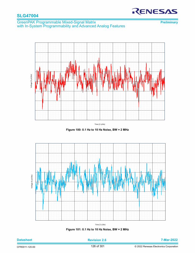
Datasheet 7-Mar-2022
CFR0011-120-00
Revision 2.6
126 of 301 © 2022 Renesas Electronics Corporation
SLG47004
GreenPAK Programmable Mixed-Signal Matrix with In-System Programmability and Advanced Analog Features
Preliminary
Figure 100: 0.1 Hz to 10 Hz Noise, BW = 2 MHz
Figure 101: 0.1 Hz to 10 Hz Noise, BW = 2 MHz
Vo
lta
ge
(5
μV
/div
)
Time (2 s/div)
Vo
lta
ge
(5
μV
/div
)
Time (2 s/div)

Datasheet 7-Mar-2022
CFR0011-120-00
Revision 2.6
127 of 301 © 2022 Renesas Electronics Corporation
SLG47004
GreenPAK Programmable Mixed-Signal Matrix with In-System Programmability and Advanced Analog Features
Preliminary
Figure 102: Channel Separation vs. Frequency
Figure 103: Op Ampx Noise Voltage Density vs. Frequency
-130
-120
-110
-100
-90
-80
-70
-60
-50
-40
-30
-20
-10
0
10 100 1 000 10 000 100 000 1 000 000 10 000 000
Ch
an
ne
l Se
pa
rati
on
(d
B)
f (Hz)
BW = 128 kHz
BW = 512 kHz
BW = 2 MHz
BW = 8 MHz
0
100
200
300
400
500
600
700
10 100 1 000 10 000 100 000 1 000 000
Inp
ut
Vo
lta
ge
No
ise
De
nsi
ty (
nV
/√H
z)
f (Hz)
BW = 128 kHz
BW = 512 kHz
BW = 2 MHz
BW = 8 MHz

Datasheet 7-Mar-2022
CFR0011-120-00
Revision 2.6
128 of 301 © 2022 Renesas Electronics Corporation
SLG47004
GreenPAK Programmable Mixed-Signal Matrix with In-System Programmability and Advanced Analog Features
Preliminary
Figure 104: Slew Rate vs. Ambient Temperature G = 1 V/V; RL = 50 kΩ for BW = 128 kHz
Figure 105: Slew Rate vs. Ambient Temperature G = 1 V/V; RL = 50 kΩ for BW = 512 kHz
50
55
60
65
70
75
80
85-4
0
-30
-20
-10 0
10
20
30
40
50
60
70
80
Sle
w R
ate
(m
V/μ
s)
T (°C)
128 kHz, 5.5 V, Falling
128 kHz, 5.5 V, Rising
128 kHz, 3.3 V, Falling
128 kHz, 3.3 V, Rising
128 kHz, 2.4 V, Falling
128 kHz, 2.4 V, Rising
220
240
260
280
300
320
340
-40
-30
-20
-10 0
10
20
30
40
50
60
70
80
Sle
w R
ate
(m
V/µ
s)
T (°C)
512 kHz, 5.5 V, Falling
512 kHz, 5.5 V, Rising
512 kHz, 3.3 V, Falling
512 kHz, 3.3 V, Rising
512 kHz, 2.4 V, Falling
512 kHz, 2.4 V, Rising

Datasheet 7-Mar-2022
CFR0011-120-00
Revision 2.6
129 of 301 © 2022 Renesas Electronics Corporation
SLG47004
GreenPAK Programmable Mixed-Signal Matrix with In-System Programmability and Advanced Analog Features
Preliminary
Figure 106: Slew Rate vs. Ambient Temperature G = 1 V/V; RL = 50 kΩ for BW = 2 MHz
Figure 107: Slew Rate vs. Ambient Temperature G = 1 V/V; RL = 50 kΩ for BW = 8 MHz
700
900
1100
1300
1500
1700
1900
2100-4
0
-30
-20
-10 0
10
20
30
40
50
60
70
80
Sle
w R
ate
(m
V/µ
s)
T (°C)
2 MHz, 5.5 V, Falling
2 MHz, 5.5 V, Rising
2 MHz, 3.3 V, Rising
2 MHz, 2.4 V, Rising
2 MHz, 3.3 V, Falling
2 MHz, 2.4 V, Falling
900
1400
1900
2400
2900
3400
3900
4400
4900
5400
-40
-30
-20
-10 0
10
20
30
40
50
60
70
80
Sle
w R
ate
(m
V/µ
s)
T (°C)
8 MHz, 5.5 V, Rising
8 MHz, 3.3 V, Rising
8 MHz, 2.4 V, Rising
8 MHz, 5.5 V, Falling
8 MHz, 2.4 V, Falling
8 MHz, 3.3 V, Falling

Datasheet 7-Mar-2022
CFR0011-120-00
Revision 2.6
130 of 301 © 2022 Renesas Electronics Corporation
SLG47004
GreenPAK Programmable Mixed-Signal Matrix with In-System Programmability and Advanced Analog Features
Preliminary
Figure 108: Small Signal Inverting Step Response G = -1 V/V, RL = 50 kΩ, CL = 60 pF, BW = 128 kHz
Figure 109: Small Signal Inverting Step Response G = -1 V/V, RL = 50 kΩ, CL = 60 pF, BW = 512 kHz
Vo
lta
ge
(1
0 m
V/d
iv)
Time (20 μs/div)
Vo
lta
ge
(1
0 m
V/d
iv)
Time (20 μs/div)

Datasheet 7-Mar-2022
CFR0011-120-00
Revision 2.6
131 of 301 © 2022 Renesas Electronics Corporation
SLG47004
GreenPAK Programmable Mixed-Signal Matrix with In-System Programmability and Advanced Analog Features
Preliminary
Figure 110: Small Signal Inverting Step Response G = -1 V/V, RL = 50 kΩ, CL = 60 pF, BW = 2 MHz
Figure 111: Small Signal Inverting Step Response G = -1 V/V, RL = 50 kΩ, CL = 60 pF, BW = 8 MHz
Vo
lta
ge
(1
0 m
V/d
iv)
Time (10 μs/div)
Vo
lta
ge
(1
0 m
V/d
iv)
Time (10 μs/div)

Datasheet 7-Mar-2022
CFR0011-120-00
Revision 2.6
132 of 301 © 2022 Renesas Electronics Corporation
SLG47004
GreenPAK Programmable Mixed-Signal Matrix with In-System Programmability and Advanced Analog Features
Preliminary
Figure 112: Small Signal Non-Inverting Step Response G = -1 V/V, RL = 50 kΩ, CL = 60 pF, BW = 128 kHz
Figure 113: Small Signal Non-Inverting Step Response G = -1 V/V, RL = 50 kΩ, CL = 60 pF, BW = 512 kHz
Vo
lta
ge
(1
0 m
V/d
iv)
Time (5 μs/div)
Vo
lta
ge
(1
0 m
V/d
iv)
Time (5 μs/div)

Datasheet 7-Mar-2022
CFR0011-120-00
Revision 2.6
133 of 301 © 2022 Renesas Electronics Corporation
SLG47004
GreenPAK Programmable Mixed-Signal Matrix with In-System Programmability and Advanced Analog Features
Preliminary
Figure 114: Small Signal Non-Inverting Step Response G = -1 V/V, RL = 50 kΩ, CL = 60 pF, BW = 2 MHz
Figure 115: Small Signal Non-Inverting Step Response G = -1 V/V, RL = 50 kΩ, CL = 60 pF, BW = 8 MHz
Vo
lta
ge
(1
0 m
V/d
iv)
Time (5 μs/div)
Vo
lta
ge
(1
0 m
V/d
iv)
Time (0.2 μs/div)
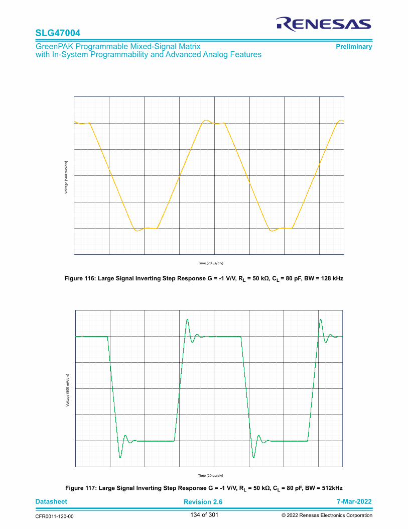
Datasheet 7-Mar-2022
CFR0011-120-00
Revision 2.6
134 of 301 © 2022 Renesas Electronics Corporation
SLG47004
GreenPAK Programmable Mixed-Signal Matrix with In-System Programmability and Advanced Analog Features
Preliminary
Figure 116: Large Signal Inverting Step Response G = -1 V/V, RL = 50 kΩ, CL = 80 pF, BW = 128 kHz
Figure 117: Large Signal Inverting Step Response G = -1 V/V, RL = 50 kΩ, CL = 80 pF, BW = 512kHz
Vo
lta
ge
(5
00
mV
/div
)
Time (20 μs/div)
Vo
lta
ge
(5
00
mV
/div
)
Time (20 μs/div)

Datasheet 7-Mar-2022
CFR0011-120-00
Revision 2.6
135 of 301 © 2022 Renesas Electronics Corporation
SLG47004
GreenPAK Programmable Mixed-Signal Matrix with In-System Programmability and Advanced Analog Features
Preliminary
Figure 118: Large Signal Inverting Step Response G = -1 V/V, RL = 50 kΩ, CL = 80 pF, BW = 2 MHz
Figure 119: Large Signal Inverting Step Response G = -1 V/V, RL = 50 kΩ, CL = 80 pF, BW = 8 MHz
Vo
lta
ge
(5
00
mV
/div
)
Time (20 μs/div)
Vo
lta
ge
(5
00
mV
/div
)
Time (20 μs/div)

Datasheet 7-Mar-2022
CFR0011-120-00
Revision 2.6
136 of 301 © 2022 Renesas Electronics Corporation
SLG47004
GreenPAK Programmable Mixed-Signal Matrix with In-System Programmability and Advanced Analog Features
Preliminary
Figure 120: Large Signal Non-Inverting Step Response G = -1 V/V, RL = 50 kΩ, CL = 60 pF, BW = 128 kHz
Figure 121: Large Signal Non-Inverting Step Response G = -1 V/V, RL = 50 kΩ, CL = 60 pF, BW = 512 kHz
Vo
lta
ge
(5
00
mV
/div
)
Time (20 μs/div)
Vo
lta
ge
(5
00
mV
/div
)
Time (20 μs/div)

Datasheet 7-Mar-2022
CFR0011-120-00
Revision 2.6
137 of 301 © 2022 Renesas Electronics Corporation
SLG47004
GreenPAK Programmable Mixed-Signal Matrix with In-System Programmability and Advanced Analog Features
Preliminary
Figure 122: Large Signal Non-Inverting Step Response G = -1 V/V, RL = 50 kΩ, CL = 60 pF, BW = 2 MHz
Figure 123: Large Signal Non-Inverting Step Response G = -1 V/V, RL = 50 kΩ, CL = 60 pF, BW = 8 MHz
Vo
lta
ge
(5
00
mV
/div
)
Time (5 μs/div)
Vo
lta
ge
(5
00
mV
/div
)
Time (2.5 μs/div)
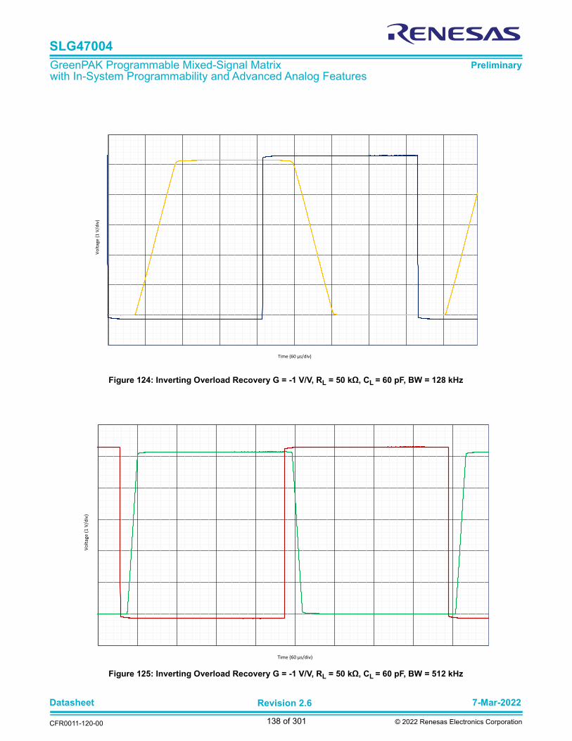
Datasheet 7-Mar-2022
CFR0011-120-00
Revision 2.6
138 of 301 © 2022 Renesas Electronics Corporation
SLG47004
GreenPAK Programmable Mixed-Signal Matrix with In-System Programmability and Advanced Analog Features
Preliminary
Figure 124: Inverting Overload Recovery G = -1 V/V, RL = 50 kΩ, CL = 60 pF, BW = 128 kHz
Figure 125: Inverting Overload Recovery G = -1 V/V, RL = 50 kΩ, CL = 60 pF, BW = 512 kHz
Vo
lta
ge
(1
V/d
iv)
Time (60 μs/div)
Vo
lta
ge
(1
V/d
iv)
Time (60 μs/div)
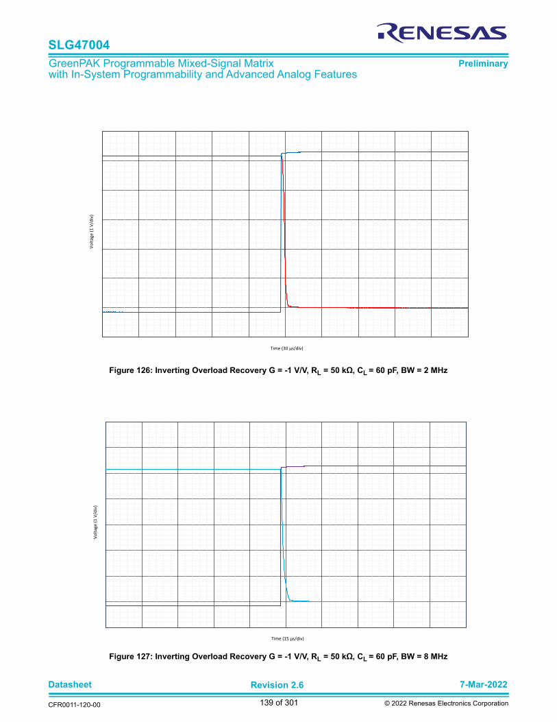
Datasheet 7-Mar-2022
CFR0011-120-00
Revision 2.6
139 of 301 © 2022 Renesas Electronics Corporation
SLG47004
GreenPAK Programmable Mixed-Signal Matrix with In-System Programmability and Advanced Analog Features
Preliminary
Figure 126: Inverting Overload Recovery G = -1 V/V, RL = 50 kΩ, CL = 60 pF, BW = 2 MHz
Figure 127: Inverting Overload Recovery G = -1 V/V, RL = 50 kΩ, CL = 60 pF, BW = 8 MHz
Vo
lta
ge
(1
V/d
iv)
Time (30 μs/div)
Vo
lta
ge
(1
V/d
iv)
Time (15 μs/div)

Datasheet 7-Mar-2022
CFR0011-120-00
Revision 2.6
140 of 301 © 2022 Renesas Electronics Corporation
SLG47004
GreenPAK Programmable Mixed-Signal Matrix with In-System Programmability and Advanced Analog Features
Preliminary
Figure 128: Non-Inverting Overload Recovery G = -1 V/V, RL = 50 kΩ, CL = 60 pF, BW = 128 kHz
Figure 129: Non-Inverting Overload Recovery G = -1 V/V, RL = 50 kΩ, CL = 60 pF, BW = 512 kHz
Vo
lta
ge
(1
V/d
iv)
Time (60 μs/div)
Vo
lta
ge
(1
V/d
iv)
Time (60 μs/div)
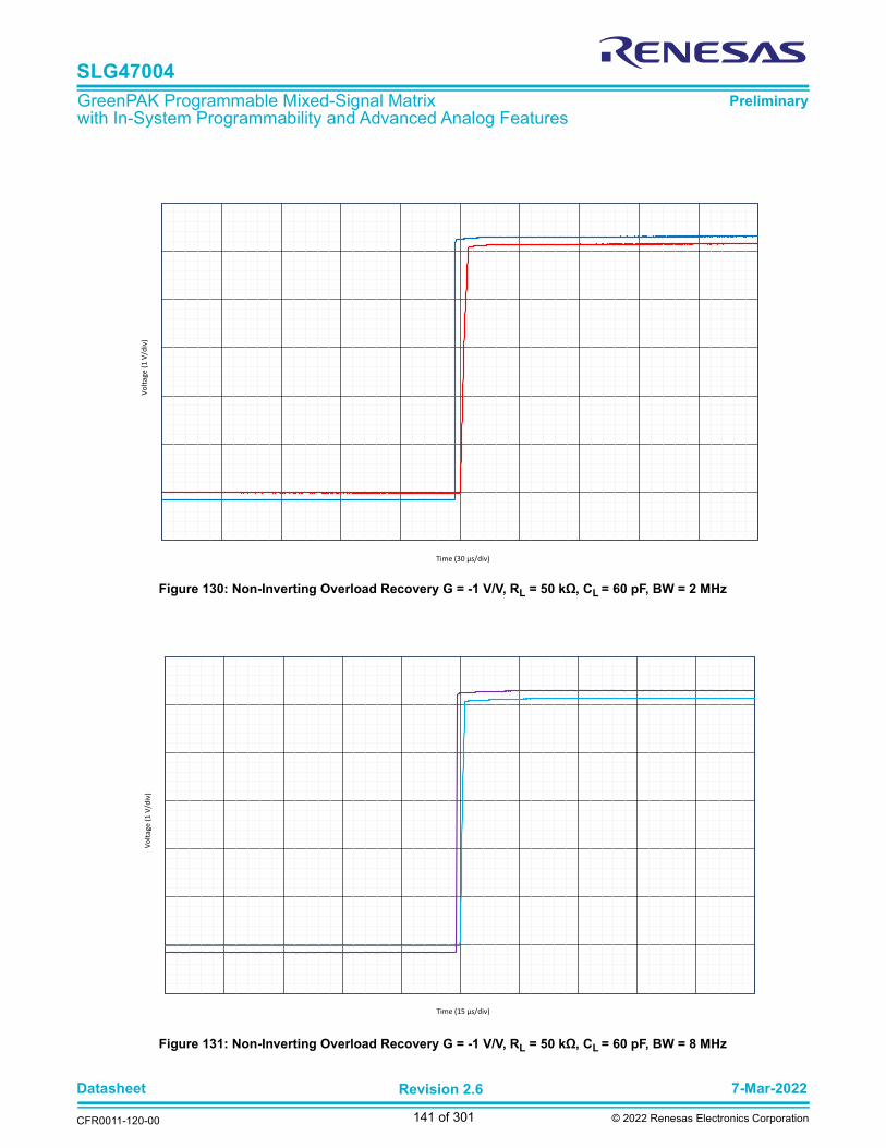
Datasheet 7-Mar-2022
CFR0011-120-00
Revision 2.6
141 of 301 © 2022 Renesas Electronics Corporation
SLG47004
GreenPAK Programmable Mixed-Signal Matrix with In-System Programmability and Advanced Analog Features
Preliminary
Figure 130: Non-Inverting Overload Recovery G = -1 V/V, RL = 50 kΩ, CL = 60 pF, BW = 2 MHz
Figure 131: Non-Inverting Overload Recovery G = -1 V/V, RL = 50 kΩ, CL = 60 pF, BW = 8 MHz
Vo
lta
ge
(1
V/d
iv)
Time (30 μs/div)
Vo
lta
ge
(1
V/d
iv)
Time (15 μs/div)
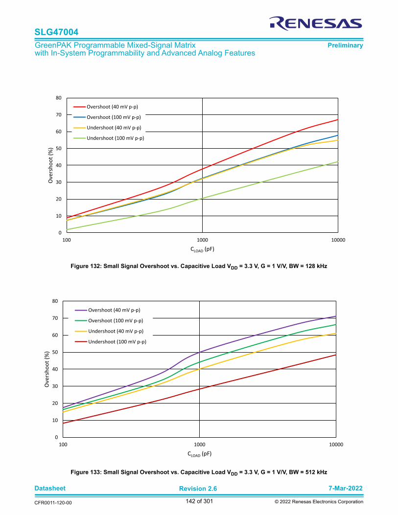
Datasheet 7-Mar-2022
CFR0011-120-00
Revision 2.6
142 of 301 © 2022 Renesas Electronics Corporation
SLG47004
GreenPAK Programmable Mixed-Signal Matrix with In-System Programmability and Advanced Analog Features
Preliminary
Figure 132: Small Signal Overshoot vs. Capacitive Load VDD = 3.3 V, G = 1 V/V, BW = 128 kHz
Figure 133: Small Signal Overshoot vs. Capacitive Load VDD = 3.3 V, G = 1 V/V, BW = 512 kHz
0
10
20
30
40
50
60
70
80
100 1000 10000
Ov
ers
ho
ot
(%)
CLOAD (pF)
Overshoot (40 mV p-p)
Overshoot (100 mV p-p)
Undershoot (40 mV p-p)
Undershoot (100 mV p-p)
0
10
20
30
40
50
60
70
80
100 1000 10000
Ov
ers
ho
ot
(%)
CLOAD (pF)
Overshoot (40 mV p-p)
Overshoot (100 mV p-p)
Undershoot (40 mV p-p)
Undershoot (100 mV p-p)

Datasheet 7-Mar-2022
CFR0011-120-00
Revision 2.6
143 of 301 © 2022 Renesas Electronics Corporation
SLG47004
GreenPAK Programmable Mixed-Signal Matrix with In-System Programmability and Advanced Analog Features
Preliminary
Figure 134: Small Signal Overshoot vs. Capacitive Load VDD = 3.3 V, G = 1 V/V, BW = 2 MHz
Figure 135: Small Signal Overshoot vs. Capacitive Load VDD = 3.3 V, G = 1 V/V, BW = 8 MHz
0
10
20
30
40
50
60
70
80
90
100 1000 10000
Ov
ers
ho
ot
(%)
CLOAD (pF)
Overshoot (40 mV p-p)
Overshoot (100 mV p-p)
Undershoot (100 mV p-p)
Undershoot (40 mV p-p)
0
10
20
30
40
50
60
70
80
90
100
Ov
ers
ho
ot
(%)
CLOAD (pF)
Undershoot (40 mV p-p)
Overshoot (40 mV p-p)
470

Datasheet 7-Mar-2022
CFR0011-120-00
Revision 2.6
144 of 301 © 2022 Renesas Electronics Corporation
SLG47004
GreenPAK Programmable Mixed-Signal Matrix with In-System Programmability and Advanced Analog Features
Preliminary
Figure 136: Output Voltage Low (VOUT - GND) vs. Temperature at BW = 128 kHz, RLOAD = 600 Ω
Figure 137: Output Voltage Low (VOUT - GND) vs. Temperature at BW = 128 kHz, RLOAD = 50 kΩ
100
110
120
130
140
150
160
170
180
190
200
210
220
-40 -30 -20 -10 0 10 20 30 40 50 60 70 80
Ou
tpu
t V
olt
ag
e (
mV
)
T (°C)
Output CM Voltage Low, Rload = 600 Ω, VDD = 5.5 V
Output CM Voltage Low, Rload = 600 Ω, VDD = 3.3 V
Output CM Voltage Low, Rload = 600 Ω, VDD = 2.4 V
0.5
0.8
1.1
1.4
1.7
2
2.3
2.6
2.9
-40 -30 -20 -10 0 10 20 30 40 50 60 70 80
Ou
tpu
t V
olt
ag
e (
mV
)
T (°C)
Output CM Voltage Low, Rload = 50 kΩ, VDD = 5.5 V
Output CM Voltage Low, Rload = 50 kΩ, VDD = 3.3 V
Output CM Voltage Low, Rload = 50 kΩ, VDD = 2.4 V
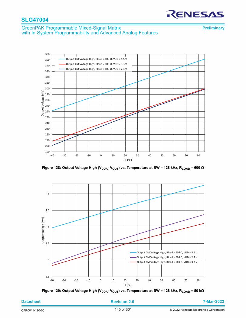
Datasheet 7-Mar-2022
CFR0011-120-00
Revision 2.6
145 of 301 © 2022 Renesas Electronics Corporation
SLG47004
GreenPAK Programmable Mixed-Signal Matrix with In-System Programmability and Advanced Analog Features
Preliminary
Figure 138: Output Voltage High (VDDA- VOUT) vs. Temperature at BW = 128 kHz, RLOAD = 600 Ω
Figure 139: Output Voltage High (VDDA- VOUT) vs. Temperature at BW = 128 kHz, RLOAD = 50 kΩ
190
200
210
220
230
240
250
260
270
280
290
300
310
320
330
340
350
360
-40 -30 -20 -10 0 10 20 30 40 50 60 70 80
Ou
tpu
t V
olt
ag
e (
mV
)
T (°C)
Output CM Voltage High, Rload = 600 Ω, VDD = 5.5 V
Output CM Voltage High, Rload = 600 Ω, VDD = 3.3 V
Output CM Voltage High, Rload = 600 Ω, VDD = 2.4 V
2.5
3
3.5
4
4.5
5
-40 -30 -20 -10 0 10 20 30 40 50 60 70 80
Ou
tpu
t V
olt
ag
e (
mV
)
T (°C)
Output CM Voltage High, Rload = 50 kΩ, VDD = 5.5 V
Output CM Voltage High, Rload = 50 kΩ, VDD = 2.4 V
Output CM Voltage High, Rload = 50 kΩ, VDD = 3.3 V

Datasheet 7-Mar-2022
CFR0011-120-00
Revision 2.6
146 of 301 © 2022 Renesas Electronics Corporation
SLG47004
GreenPAK Programmable Mixed-Signal Matrix with In-System Programmability and Advanced Analog Features
Preliminary
Figure 140: Output Voltage Low (VOUT - GND) vs. Temperature at BW = 512 kHz, RLOAD = 50 kΩ
Figure 141: Output Voltage Low (VOUT - GND) vs. Temperature at BW = 512 kHz, RLOAD = 50 kΩ
90
100
110
120
130
140
150
160
170
180
-40 -30 -20 -10 0 10 20 30 40 50 60 70 80
Ou
tpu
t V
olt
ag
e (
mV
)
T (°C)
Output CM Voltage Low, Rload = 600 Ω, VDD = 5.5 V
Output CM Voltage Low, Rload = 600 Ω, VDD = 3.3 V
Output CM Voltage Low, Rload = 600 Ω, VDD = 2.4 V
0.5
1
1.5
2
2.5
-40 -30 -20 -10 0 10 20 30 40 50 60 70 80
Ou
tpu
t V
olt
ag
e (
mV
)
T (°C)
Output CM Voltage Low, Rload = 50 kΩ, VDD = 5.5 V
Output CM Voltage Low, Rload = 50 kΩ, VDD = 3.3 V
Output CM Voltage Low, Rload = 50 kΩ, VDD = 2.4 V

Datasheet 7-Mar-2022
CFR0011-120-00
Revision 2.6
147 of 301 © 2022 Renesas Electronics Corporation
SLG47004
GreenPAK Programmable Mixed-Signal Matrix with In-System Programmability and Advanced Analog Features
Preliminary
Figure 142: Output Voltage High (VDDA- VOUT) vs. Temperature at BW = 512 kHz, RLOAD = 600 Ω
Figure 143: Output Voltage High (VDDA- VOUT) vs. Temperature at BW = 512kHz, RLOAD = 50 kΩ
150
170
190
210
230
250
270
290
-40 -30 -20 -10 0 10 20 30 40 50 60 70 80
Ou
tpu
t V
olt
ag
e (
mV
)
T (°C)
Output CM Voltage High, Rload = 600 Ω, VDD = 5.5 V
Output CM Voltage High, Rload = 600 Ω, VDD = 3.3 V
Output CM Voltage High, Rload = 600 Ω, VDD = 2.4 V
2
2.3
2.6
2.9
3.2
3.5
3.8
4.1
4.4
-40 -30 -20 -10 0 10 20 30 40 50 60 70 80
Ou
tpu
t V
olt
ag
e (
mV
)
T (°C)
Output CM Voltage High, Rload = 50 kΩ, VDD = 5.5 V
Output CM Voltage High, Rload = 50 kΩ, VDD = 2.4 V
Output CM Voltage High, Rload = 50 kΩ, VDD = 3.3 V

Datasheet 7-Mar-2022
CFR0011-120-00
Revision 2.6
148 of 301 © 2022 Renesas Electronics Corporation
SLG47004
GreenPAK Programmable Mixed-Signal Matrix with In-System Programmability and Advanced Analog Features
Preliminary
Figure 144: Output Voltage Low (VOUT - GND) vs. Temperature at BW = 2 MHz, RLOAD = 600 Ω
Figure 145: Output Voltage Low (VOUT - GND) vs. Temperature at BW = 2 MHz, RLOAD = 50 kΩ
60
70
80
90
100
110
120
130
140
-40 -30 -20 -10 0 10 20 30 40 50 60 70 80
Ou
tpu
t V
olt
ag
e (
mV
)
T (°C)
Output CM Voltage Low, Rload = 600 Ω, VDD = 5.5 V
Output CM Voltage Low, Rload = 600 Ω, VDD = 3.3 V
Output CM Voltage Low, Rload = 600 Ω, VDD = 2.4 V
0
0.5
1
1.5
2
2.5
-40 -30 -20 -10 0 10 20 30 40 50 60 70 80
Ou
tpu
t V
olt
ag
e (
mV
)
T (°C)
Output CM Voltage Low, Rload = 50 kΩ, VDD = 5.5 V
Output CM Voltage Low, Rload = 50 kΩ, VDD = 3.3 V
Output CM Voltage Low, Rload = 50 kΩ, VDD = 2.4 V

Datasheet 7-Mar-2022
CFR0011-120-00
Revision 2.6
149 of 301 © 2022 Renesas Electronics Corporation
SLG47004
GreenPAK Programmable Mixed-Signal Matrix with In-System Programmability and Advanced Analog Features
Preliminary
Figure 146: Output Voltage High (VDDA- VOUT) vs. Temperature at BW = 2 MHz, RLOAD = 600 Ω
Figure 147: Output Voltage High (VDDA- VOUT) vs. Temperature at BW = 2 MHz, RLOAD = 50 kΩ
100
120
140
160
180
200
220
-40 -30 -20 -10 0 10 20 30 40 50 60 70 80
Ou
tpu
t V
olt
ag
e (
mV
)
T (°C)
Output CM Voltage High, Rload = 600 Ω, VDD = 5.5 V
Output CM Voltage High, Rload = 600 Ω, VDD = 2.4 V
Output CM Voltage High, Rload = 600 Ω, VDD = 3.3 V
1.6
1.8
2
2.2
2.4
2.6
2.8
3
3.2
3.4
3.6
-40 -30 -20 -10 0 10 20 30 40 50 60 70 80
Ou
tpu
t V
olt
ag
e (
mV
)
T (°C)
Output CM Voltage High, Rload = 50 kΩ, VDD = 5.5 V
Output CM Voltage High, Rload = 50 kΩ, VDD = 2.4 V
Output CM Voltage High, Rload = 50 kΩ, VDD = 3.3 V

Datasheet 7-Mar-2022
CFR0011-120-00
Revision 2.6
150 of 301 © 2022 Renesas Electronics Corporation
SLG47004
GreenPAK Programmable Mixed-Signal Matrix with In-System Programmability and Advanced Analog Features
Preliminary
Figure 148: Output Voltage Low (VOUT - GND) vs. Temperature at BW = 8MHz, RLOAD = 600 Ω
Figure 149: Output Voltage Low (VOUT - GND) vs. Temperature at BW = 8 MHz, RLOAD = 50 kΩ
40
50
60
70
80
90
100
-40 -30 -20 -10 0 10 20 30 40 50 60 70 80
Ou
tpu
t V
olt
ag
e (
mV
)
T (°C)
Output CM Voltage Low, Rload = 600 Ω, VDD = 5.5 V
Output CM Voltage Low, Rload = 600 Ω, VDD = 3.3 V
Output CM Voltage Low, Rload = 600 Ω, VDD = 2.4 V
0.3
0.5
0.7
0.9
1.1
1.3
1.5
1.7
-40 -30 -20 -10 0 10 20 30 40 50 60 70 80
Ou
tpu
t V
olt
ag
e (
mV
)
T (°C)
Output CM Voltage Low, Rload = 50 kΩ, VDD = 5.5 V
Output CM Voltage Low, Rload = 50 kΩ, VDD = 3.3 V
Output CM Voltage Low, Rload = 50 kΩ, VDD = 2.4 V
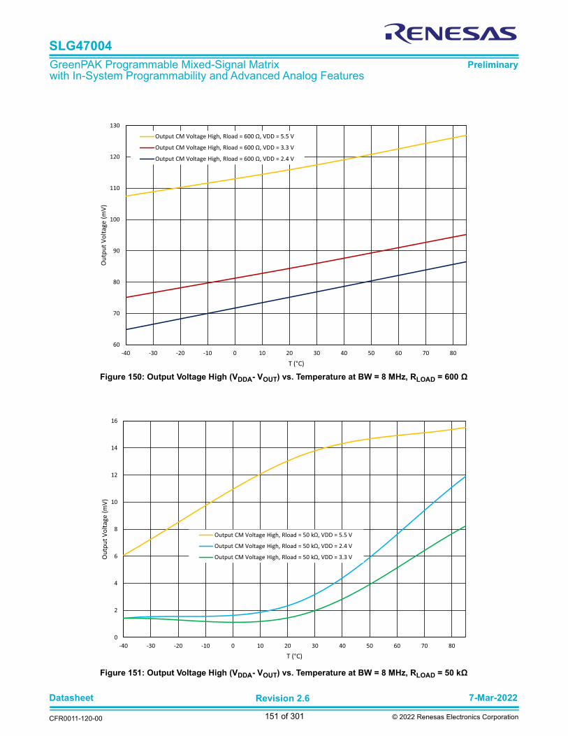
Datasheet 7-Mar-2022
CFR0011-120-00
Revision 2.6
151 of 301 © 2022 Renesas Electronics Corporation
SLG47004
GreenPAK Programmable Mixed-Signal Matrix with In-System Programmability and Advanced Analog Features
Preliminary
Figure 150: Output Voltage High (VDDA- VOUT) vs. Temperature at BW = 8 MHz, RLOAD = 600 Ω
Figure 151: Output Voltage High (VDDA- VOUT) vs. Temperature at BW = 8 MHz, RLOAD = 50 kΩ
60
70
80
90
100
110
120
130
-40 -30 -20 -10 0 10 20 30 40 50 60 70 80
Ou
tpu
t V
olt
ag
e (
mV
)
T (°C)
Output CM Voltage High, Rload = 600 Ω, VDD = 5.5 V
Output CM Voltage High, Rload = 600 Ω, VDD = 3.3 V
Output CM Voltage High, Rload = 600 Ω, VDD = 2.4 V
0
2
4
6
8
10
12
14
16
-40 -30 -20 -10 0 10 20 30 40 50 60 70 80
Ou
tpu
t V
olt
ag
e (
mV
)
T (°C)
Output CM Voltage High, Rload = 50 kΩ, VDD = 5.5 V
Output CM Voltage High, Rload = 50 kΩ, VDD = 2.4 V
Output CM Voltage High, Rload = 50 kΩ, VDD = 3.3 V
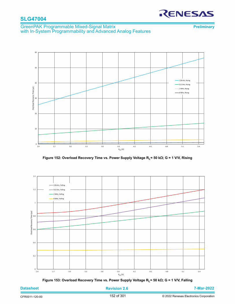
Datasheet 7-Mar-2022
CFR0011-120-00
Revision 2.6
152 of 301 © 2022 Renesas Electronics Corporation
SLG47004
GreenPAK Programmable Mixed-Signal Matrix with In-System Programmability and Advanced Analog Features
Preliminary
Figure 152: Overload Recovery Time vs. Power Supply Voltage RL= 50 kΩ; G = 1 V/V, Rising
Figure 153: Overload Recovery Time vs. Power Supply Voltage RL= 50 kΩ; G = 1 V/V, Falling
0
10
20
30
40
50
60
2.4 2.7 3.0 3.3 3.6 3.9 4.2 4.5 4.8 5.1 5.4
Ove
rlo
ad
Re
cove
ry T
ime
(μ
s)
VDD (V)
128 kHz, Rising
512 kHz, Rising
2 MHz, Rising
8 MHz, Rising
0
0.2
0.4
0.6
0.8
1
1.2
1.4
2.4 2.7 3.0 3.3 3.6 3.9 4.2 4.5 4.8 5.1 5.4
Ov
erl
oa
d R
eco
ve
ry T
ime
(μ
s)
VDD (V)
128 kHz, Falling
512 kHz, Falling
2 MHz, Falling
8 MHz, Falling

Datasheet 7-Mar-2022
CFR0011-120-00
Revision 2.6
153 of 301 © 2022 Renesas Electronics Corporation
SLG47004
GreenPAK Programmable Mixed-Signal Matrix with In-System Programmability and Advanced Analog Features
Preliminary
Figure 154: Output Response to Power Down Signal G = 1 V/V; RL = 50 kΩ; CL = 20 pF; VIN = VS/2, BW = 128 kHz
Figure 155: Output Response to Power Down Signal G = 1 V/V; RL = 50 kΩ; CL = 20 pF; VIN = VS/2, BW = 512 kHz
Vo
lta
ge
(1
V/d
iv)
Time (10 μs/div)
Vo
lta
ge
(1
V/d
iv)
Time (2 μs/div)

Datasheet 7-Mar-2022
CFR0011-120-00
Revision 2.6
154 of 301 © 2022 Renesas Electronics Corporation
SLG47004
GreenPAK Programmable Mixed-Signal Matrix with In-System Programmability and Advanced Analog Features
Preliminary
Figure 156: Output Response to Power Down Signal G = 1 V/V; RL = 50 kΩ; CL = 20 pF; VIN = VS/2, BW = 2 MHz
Figure 157: Output Response to Power Down Signal G = 1 V/V; RL = 50 kΩ; CL = 20 pF; VIN = VS/2, BW = 8 MHz
Vo
lta
ge
(1
V/d
iv)
Time (1 μs/div)
Vo
lta
ge
(1
V/d
iv)
Time (1 μs/div)

Datasheet 7-Mar-2022
CFR0011-120-00
Revision 2.6
155 of 301 © 2022 Renesas Electronics Corporation
SLG47004
GreenPAK Programmable Mixed-Signal Matrix with In-System Programmability and Advanced Analog Features
Preliminary
Figure 158: Opampx Turn-On/Off Time vs. VDD at VIN = VDD/2, BW = 128 kHz
Figure 159: Opampx Turn-On/Off Time vs. VDD at VIN = VDD/2, BW = 512 kHz
15
20
25
30
35
40
2.4 2.7 3.0 3.3 3.6 3.9 4.2 4.5 4.8 5.1 5.4
Tu
rn -
On
/Off
Tim
e (
μs)
VDD (V)
Turn-On Time @ T = -40 °C
Turn-On Time @ T = 25 °C
Turn-On Time @ T = 85 °C
Turn-Off Time @ T = -40 °C
Turn-Off Time @ T = 25 °C
Turn-Off Time @ T = 85 °C
2
4
6
8
10
12
14
16
18
20
2.4 2.7 3.0 3.3 3.6 3.9 4.2 4.5 4.8 5.1 5.4
Tu
rn -
On
/Off
Tim
e (
μs)
VDD (V)
Turn-Off Time @ T = -40 °C
Turn-Off Time @ T = 25 °C
Turn-Off Time @ T = 85 °C
Turn-On Time @ T = -40 °C
Turn-On Time @ T = 25 °C

Datasheet 7-Mar-2022
CFR0011-120-00
Revision 2.6
156 of 301 © 2022 Renesas Electronics Corporation
SLG47004
GreenPAK Programmable Mixed-Signal Matrix with In-System Programmability and Advanced Analog Features
Preliminary
Figure 160: Opampx Turn-On/Off Time vs. VDD at VIN = VDD/2, BW = 2 MHz
Figure 161: Opampx Turn-On/Off Time vs. VDD at VIN = VDD/2, BW = 8MHz
0
2
4
6
8
10
12
14
16
18
2.4 2.7 3.0 3.3 3.6 3.9 4.2 4.5 4.8 5.1 5.4
Tu
rn -
On
/Off
Tim
e (
μs)
VDD (V)
Turn-Off Time @ T = -40 °CTurn-Off Time @ T = 25 °CTurn-Off Time @ T = 85 °CTurn-On Time @ T = -40 °CTurn-On Time @ T = 25 °CTurn-On Time @ T = 85 °C
0
2
4
6
8
10
12
14
16
18
2.4 2.7 3.0 3.3 3.6 3.9 4.2 4.5 4.8 5.1 5.4
Tu
rn -
On
/Off
Tim
e (
μs)
VDD (V)
Turn-Off Time @ T = -40 °C
Turn-Off Time @ T = 25 °C
Turn-Off Time @ T = 85 °C
Turn-On Time @ T = -40 °C
Turn-On Time @ T = 25 °C
Turn-On Time @ T = 85 °C
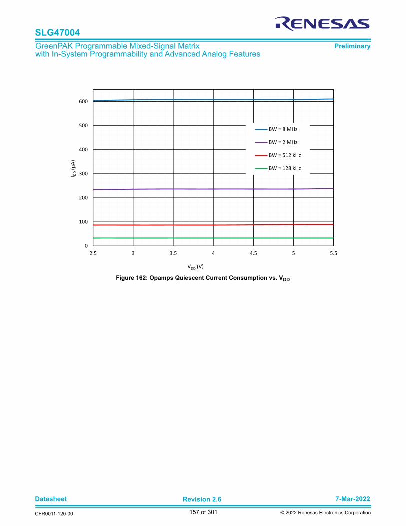
Datasheet 7-Mar-2022
CFR0011-120-00
Revision 2.6
157 of 301 © 2022 Renesas Electronics Corporation
SLG47004
GreenPAK Programmable Mixed-Signal Matrix with In-System Programmability and Advanced Analog Features
Preliminary
Figure 162: Opamps Quiescent Current Consumption vs. VDD
0
100
200
300
400
500
600
2.5 3 3.5 4 4.5 5 5.5
I DD(μA
)
VDD (V)
BW = 8 MHz
BW = 2 MHz
BW = 512 kHz
BW = 128 kHz

Datasheet 7-Mar-2022
CFR0011-120-00
Revision 2.6
158 of 301 © 2022 Renesas Electronics Corporation
SLG47004
GreenPAK Programmable Mixed-Signal Matrix with In-System Programmability and Advanced Analog Features
Preliminary
11 Analog Switch Macrocell
11.1 ANALOG SWITCH GENERAL DESCRIPTION
The SLG47004 contains two single-pole/single throw (SPST) normally open analog switches (AS). The structure of the AnalogSwitches is shown in Figure 163 and Figure 164.
Each analog switch can be controlled from the following sources:
Connection matrix Operational Amplifier macrocell.
Small NMOS (small PMOS) of Analog Switch must be enabled when macrocell is controlled by logic signal from connectionmatrix. Otherwise, small NMOS (small PMOS) must be disabled when macrocell is controlled by op amp.
Table 57 and Table 58 show possible operation modes of analog switches.
Figure 163: Analog Switch 0 Control Circuit

Datasheet 7-Mar-2022
CFR0011-120-00
Revision 2.6
159 of 301 © 2022 Renesas Electronics Corporation
SLG47004
GreenPAK Programmable Mixed-Signal Matrix with In-System Programmability and Advanced Analog Features
Preliminary
Figure 164: Analog Switch 1 Control Circuit
Table 57: Analog Switch 0 Modes of Operation
Mode of Operation
Half Bridge Mode Enable Register [740]
Matrix/Op Amp Control
Register [738]
Small nMOS Enable
Register [736]
Analog Switch mode with big pMOS only (control from connection matrix) 0 0 0
Analog Switch mode with all FETs enabled (control from connection matrix) 0 0 1
Voltage Regulator mode 0 1 0
Half Bridge mode with big pMOS only (control from connection ma-trix) 1 x 0
Half Bridge mode with all FETs enabled (control from connection matrix) 1 x 1
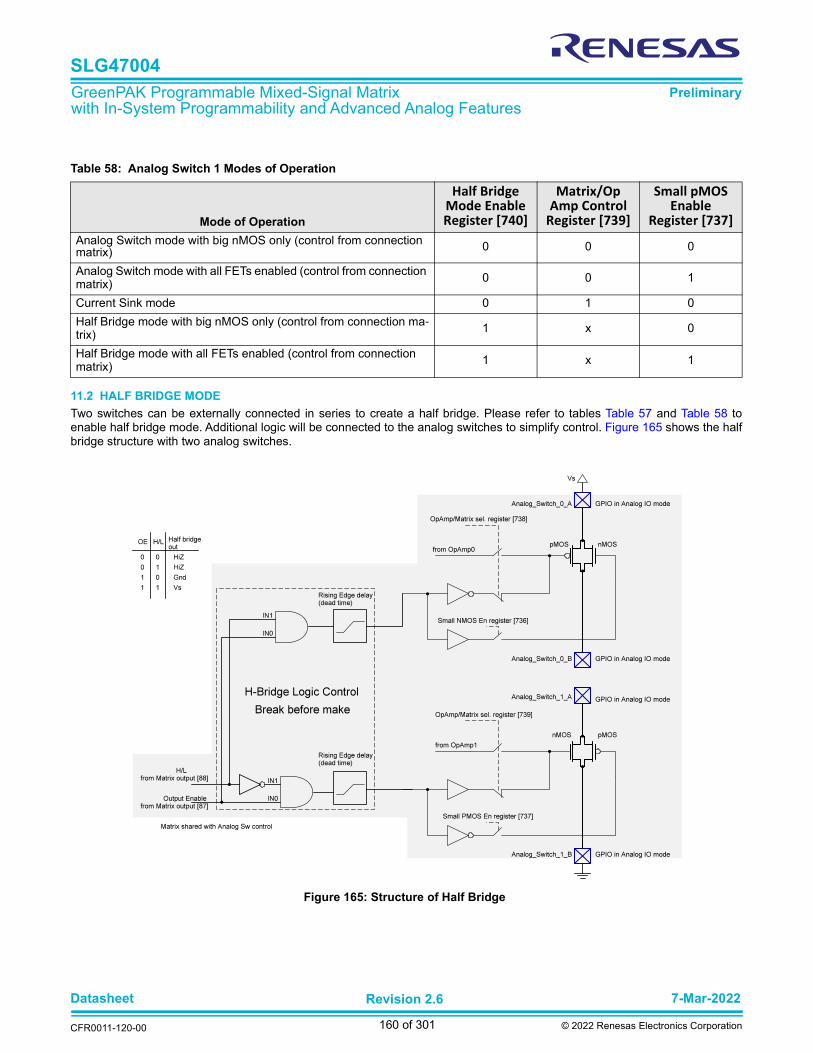
Datasheet 7-Mar-2022
CFR0011-120-00
Revision 2.6
160 of 301 © 2022 Renesas Electronics Corporation
SLG47004
GreenPAK Programmable Mixed-Signal Matrix with In-System Programmability and Advanced Analog Features
Preliminary
11.2 HALF BRIDGE MODE
Two switches can be externally connected in series to create a half bridge. Please refer to tables Table 57 and Table 58 toenable half bridge mode. Additional logic will be connected to the analog switches to simplify control. Figure 165 shows the halfbridge structure with two analog switches.
Table 58: Analog Switch 1 Modes of Operation
Mode of Operation
Half Bridge Mode Enable Register [740]
Matrix/Op Amp Control
Register [739]
Small pMOS Enable
Register [737]
Analog Switch mode with big nMOS only (control from connection matrix) 0 0 0
Analog Switch mode with all FETs enabled (control from connection matrix) 0 0 1
Current Sink mode 0 1 0
Half Bridge mode with big nMOS only (control from connection ma-trix) 1 x 0
Half Bridge mode with all FETs enabled (control from connection matrix) 1 x 1
Figure 165: Structure of Half Bridge

Datasheet 7-Mar-2022
CFR0011-120-00
Revision 2.6
161 of 301 © 2022 Renesas Electronics Corporation
SLG47004
GreenPAK Programmable Mixed-Signal Matrix with In-System Programmability and Advanced Analog Features
Preliminary
11.3 ANALOG SWITCHES TYPICAL PERFORMANCE
Figure 166: Typical RON vs. Input Voltage (Vi) for Vi = 0 to VDDA, ILOAD = 1 mA, VDDA = 2.4 V
Figure 167: Typical RON vs. Input Voltage (Vi) for Vi = 0 to VDDA, ILOAD = 1 mA, VDDA = 5.5 V
0
10
20
30
40
50
60
70
0 0.2 0.4 0.6 0.8 1 1.2 1.4 1.6 1.8 2 2.2 2.4
RD
S(O
N)(Ω
)
VIN (V)
AS0 VDD = 2.4 V
AS1 VDD = 2.4 V
0
5
10
15
20
25
30
35
40
0 0.5 1 1.5 2 2.5 3 3.5 4 4.5 5 5.5
RD
S(O
N)(Ω
)
VIN (V)
AS0 VDD = 5.5 V
AS1 VDD = 5.5 V

Datasheet 7-Mar-2022
CFR0011-120-00
Revision 2.6
162 of 301 © 2022 Renesas Electronics Corporation
SLG47004
GreenPAK Programmable Mixed-Signal Matrix with In-System Programmability and Advanced Analog Features
Preliminary
Figure 168: Turn-On Time vs. VDD at RLOAD = 100 Ω to GND, VIN = VDD/2
Figure 169: Turn-Off Time vs. VDD at RLOAD = 100 Ω to GND, VIN = VDD/2
40
60
80
100
120
140
160
180
200
220
240
2.4 2.7 3.0 3.3 3.6 3.9 4.2 4.5 4.8 5.1 5.4
Tu
rn -
On
Tim
e (
ns)
VDD (V)
AS0 (T = -40 °C) AS0 (T = 25 °C) AS0 (T = 85 °C)
AS1 (T = -40°C) AS1 (T = 25 °C) AS1 (T = 85 °C)
50
100
150
200
250
300
350
400
450
2.4 2.7 3.0 3.3 3.6 3.9 4.2 4.5 4.8 5.1 5.4
Tu
rn -
Off
Tim
e (
ns)
VDD (V)
AS0 (T = -40 °C) AS0 (T = 25 °C) AS0 (T = 85 °C)
AS1 (T = -40°C) AS1 (T = 25 °C) AS1 (T = 85 °C)

Datasheet 7-Mar-2022
CFR0011-120-00
Revision 2.6
163 of 301 © 2022 Renesas Electronics Corporation
SLG47004
GreenPAK Programmable Mixed-Signal Matrix with In-System Programmability and Advanced Analog Features
Preliminary
12 Digital Rheostats and Programmable Trim Block
The SLG47004 contains two 10-bit Digital Rheostats. The structure of both macrocells is shown in Figure 170. The range ofdigital code that corresponds to the rheostat resistance ranges from 0 to 1023 (1024 taps). Code 0 corresponds to the minimumresistance between the RHx_A and RHx_B terminals. As the code value increases, the resistance between the RHx_A andRHx_B terminals monotonically increases. Consequently, when the code value decreases, the resistance between the RH0_Aand RH0_B terminals decreases as well (see Section 12.2). The voltage on any rheostat pin can be in the range from AGND toVDDA, as well as be dynamically changed during operation.
To guarantee proper operation of digital rheostats charge pump must be turned on (matrix input [86] must be logic High orregisters [912] = 1, [913] = 1). Optionally user can turn off rheostats charge pump to decrease energy consumption. But it'sstrongly recommended to use the charge pump if VDD < 4.5 V.
The rheostat resistance can be changed in three ways:
Changing the Rheostat value using the I2C interface; Manually changing the rheostat value using clock and up/down signals, similar to the counter; Using the Built-in Auto-Trim mode, where the rheostat value change is done using a special logic based on the signal from
the Chopper ACMP.Each rheostat also has three Switching Speed Modes:
Regular mode (Register [915] = 0, Register [914] = 0) - up to 1 kHz. In this mode, Low Power Bandgap Chopper Oscillator that oscillates around 120 kHz is used as a source for the charge pump clock. This setting has a lower quiescent current at the expense of a longer recovery time after input voltage spikes.
Fast mode (Register [915] = 0, Register [914] = 1) - up to 100 kHz. In this mode, the 2 MHz OSC is used as a source for the charge pump clock. This setting has a faster recovery time for input voltage spikes at the expense of a larger quiescent current. Please note that this selection forces On the OSC1 (2.048 MHz).
Auto Selection (Register [915] = 1, Register [914] = either) when trim is used. When Auto-Trim is active, the fast mode is used. After the Auto-Trim process completes, the regular mode is used.
Note: The maximum switching speed can be achieved if no external capacitive load is connected to the rheostat terminals.
The Programmable Trim (PT) blocks of rheostats macrocell contain analog MUXs, digital MUXs, Chopper ACMP, and additionallogic. The two analog MUXs (M1 and M2) and the Chopper ACMP are both shared between the two rheostats. All analog anddigital MUXs are set by NVM bits and can be overwritten with I2C.
The M_CK0 and M_CK1 MUXs select the clock source from internal pre-dividers of the internal oscillators or from theconnection matrix. The internal clock sources for the rheostats are OSC0, OSC0/8, OSC0/64, OSC0/512, OSC0/4096,OSC0/32768, OSC0/262144, OSC1, OSC1/8, OSC1/64, and OSC1/512. The PT blocks of the rheostat use the same clockscheme as Counter/Delay Macrocells (refer to 16.5). M_CH0 and M_CH1 select the Chopper comparator or a matrix output asthe signal source for the main rheostat up/down counter direction. The output of the Chopper ACMP is connected with theUp/Down inputs of the PT blocks by default. The output of the Chopper ACMP can be optionally inverted by setting register[882] to “1”.
M1 MUX selects the input for the Chopper comparator to be connected either internally to one of 3 integrated op amps (OpAmp0 out, Op Amp1 out, In Amp Out) or externally to a PIN. M2 MUX is simplified symbol of Chopper ACMP reference selectionblocks. The Chopper ACMP reference ("-" input) can be: analog signal from pin, divided internal Vref voltage (6-bit divider), ordivide VDDA voltage (6-bit divider). In Auto-Trim mode each of Rheostats has it own settings for Chopper ACMP inputs. For moreinformation about Chopper ACMP Vref see Section 9.2.
The power-up signal for the Chopper ACMP can be handled either by matrix output signal or Set0/Set1 signal from the PTmacrocell. In Auto-Trim mode (Auto_Cal _Dis_RHx NVM bit = 0) additional internal logic enables the clocking of thecorresponding PT macrocell counter and disables clocking when one of the stop conditions is reached. See a detaileddescription in Section 12.4. In Figure 170 when Auto_Cal _Dis_RHx NVM bit = 0 (Auto-Trim mode is enabled), the clockingpulses for the internal PT macrocell counter are under control of additional logic. When Auto_Cal _Dis_RHx NVM bit = 1 (Auto-Trim mode is disabled), all additional logics (Set signal, internal Set signal, Idle/Active signal) operate the same way, but clockpulses are always enabled and generated externally by the user. Calibration channel can be selected automatically (1st channelis channel 0, second channel is channel 1) or can be set manually by registers [893:892].
The inputs of Chopper ACMP can be reconfigured while operating in Auto-Trim mode. There is one configuration of inputs (M1,M2 configuration, Figure 170) for the case when Set0 signal is latched, and another configuration of M1, M2 MUXs when Set1signal is latched. For example, M1 MUX can be configured to operate with In Amp out when Set0 is latched andChopper_ACMP+ pin when Set1 is latched. The same way, M2 can be configured to work with any of M2 inputs when Set0 orSet1 are latched. Note that the default configuration is the configuration for Set0 signal. When Chopper ACMP operates asseparate ACMP and Auto-Trim function is disabled, M1 and M2 MUXs operates with configuration for Set0 signal.

Datasheet 7-Mar-2022
CFR0011-120-00
Revision 2.6
164 of 301 © 2022 Renesas Electronics Corporation
SLG47004
GreenPAK Programmable Mixed-Signal Matrix with In-System Programmability and Advanced Analog Features
Preliminary
Keep in mind that two Auto-Trim processes cannot be done simultaneously. When the Auto-Trim process for one rheostat isactive, all signals on the Set input for another rheostat will be ignored. See a detailed description in 12.4.1. The initial userdefined value of Digital Rheostat resistance can be programmed into the NVM. The initial value will be loaded during the Power-On event and this value will be used as the initial rheostat resistance, as well as a starting point for count down or count up.
Both read and write operations are allowed for rheostat resistance value, stored in NVM. Also, both read and write operationsare allowed for current rheostat resistance value. RH0 read operation - registers [1561:1552], write operation - registers[1545:1536]. RH1 read operation - registers [1689:1680], write operation - registers [1673:1664].

Datasheet 7-Mar-2022
CFR0011-120-00
Revision 2.6
165 of 301 © 2022 Renesas Electronics Corporation
SLG47004
GreenPAK Programmable Mixed-Signal Matrix with In-System Programmability and Advanced Analog Features
Preliminary
Figure 170: Programmable Trim Blocks and Digital Rheostat’s Internal Circuit

Datasheet 7-Mar-2022
CFR0011-120-00
Revision 2.6
166 of 301 © 2022 Renesas Electronics Corporation
SLG47004
GreenPAK Programmable Mixed-Signal Matrix with In-System Programmability and Advanced Analog Features
Preliminary
PT macrocell signals:
“Set”: external Set signal begins the Auto-Trim process when Auto_Cal _Dis_RHx bit is cleared (registers [901]). Otherwise, this signal has no effect. The behavior of the PT macrocell in Auto-Trim mode is described below.
“Reload”: when Reload goes high the rheostat value stored in the MTP NVM will be loaded into the rheostat (Register and Counter) overwriting any current setting. This signal is edge sensitive. It has no effect while the Auto-Trim procedure is active. For detailed information see Section 12.3.
“Program”: when Program goes high the Internal Counter value of the rheostat will be programmed into the MTP overwriting any current value in the NVM. This procedure can be done up to 1000 times. This signal is also edge sensitive. It has no effect while the Auto-Trim procedure is active. For detailed information see 12.3. To enable "Program" signal from connection matrix RH_PRB register must be cleared (RH_PRB [1796] = 0). If RH_PRB [1796] register is set to 1, the access to NVM is disabled for "Program" signal. Refer to Section 19.6 for more details.
“Clock”: this input has the following options: the PT macrocell can be clocked internally or from matrix. When clocked internally, the clock is automatically enabled/disabled by the Set input logic in Auto-Trim mode. The internal clock is synchronized with the Chopper ACMP clock.
“Up/Down”: the rheostat counter counts up when the signal is High and down when the signal is Low. “Idle/Active”: this is the connection matrix input, that is logic HIGH by default. It goes LOW with rising edge on SET input ifAuto-Trim mode is enabled (Auto_Cal _Dis_RHx NVM bit = 0). After the end of Auto-Trim procedure (one of stop conditionsoccurs) this signal sets to logic HIGH again. “FIFO nReset”: low level at this input clears internal FIFO buffer for commands Reload and Program for both rheostats. User
should provide high logic level at this input for the normal rheostat operation.
There is also an overflow protection option, for which the counter will stop counting up when the maximum value (0x3FF) isreached or stop counting down when the minimum value (0x00) is reached. The digital rheostat is initialized/powered in the firstplace. The rheostat value is Hi-Z (or highest resistance if it is impossible to disconnect the rheostat) during the Power-Onsequence.
12.1 POTENTIOMETER MODE
This mode allows two 2-pin rheostats to work as one 3-pin potentiometer. When this mode is active (register [917] = 1), userchanges the value of RH0 internal counter. In this mode, the value of RH1 counter is the inverted value of RH0 counter (Figure171). Note that the RH0_B pin and the RH1_A pin must be connected externally. Also, note that the Auto-Trim function isn'tallowed in Potentiometer Mode.
12.2 CALCULATING ACTUAL RESISTANCE
In applications where the absolute rheostat resistance is critical, the user can calculate it using the rheostat tolerance data, theminimum rheostat resistance, and the desired code.
The 16-bit tolerance data for both rheostats has been programmed into registers 0xE6 to 0xE9. These registers can be used tocalculate the total rheostat resistance. The 16th bit defines the sign (0 = +, 1 = -) of the tolerance. The other fifteen bitscorrespond to the absolute value of the rheostat tolerances variation from 100 kΩ measured at 25 °C.
Figure 171: Rheostats in Potentiometer Mode

Datasheet 7-Mar-2022
CFR0011-120-00
Revision 2.6
167 of 301 © 2022 Renesas Electronics Corporation
SLG47004
GreenPAK Programmable Mixed-Signal Matrix with In-System Programmability and Advanced Analog Features
Preliminary
Note that the rheostat tolerance data is programmed into registers 0xE6 to 0xE9. To avoid losing this tolerance data, specialattention must be paid when erasing and reprogramming page 14 in the NVM.
The rheostat value at a given code depends on the total digital rheostat resistance. The equations below can be used tocalculate the rheostat resistance.
where:
RCode - Rheostat Resistance at a Given Code;
RDR - Total Digital Rheostat Resistance;
RDR MIN - Minimum Rheostat Resistance;
code - Rheostat Position Ranging from 0x000 to 0x3FF;signRH_Tolerance - the MSB of the Rheostat’s Tolerance Data;
RRH_Tolerance - the 15 LSBs of the Rheostat’s Tolerance Data.
For example, let's say that 0x2B67 has been written into the rheostat tolerance registers within the GreenPAK's NVM. B15corresponds to a positive sign while B14:0 translates into a decimal value of 11111. RDR calculates to approximately 111,111 Ω
and can be used with the minimum rheostat resistance to calculate the resistance at a given code. Note that the minimumrheostat resistance must be measured to obtain precise results, but a range is provided in Table 25.
12.3 DIGITAL RHEOSTAT VALUE SELF-PROGRAMMING INTO THE NVM
The current value of rheostat is stored in the Internal Counter. This value can be programmed into the MTP by setting logicHIGH at "Program" input. In this case, SLG47004 will generate a specific memory control sequence to rewrite a new value intothe NVM. There is a separate NVM page that is dedicated for the Digital Rheostat value.
There is a dedicated bit RH_PRB, that enables/disables "Program" signal of PT block to change NVM rheostats resistancevalues. If RH_PRB[1796] = 0, "Program" signal is enabled. If RH_PRB[1796] = 1, "Program" signal is disabled. Note that
RH_PRB bit has no effect on I2C access to NVM. To enable/disable I2C access to rheostat resistance value, stored in NVM,user must change NPRB0, NPRB1 bits. Refer to Section 18.5.
SLG47004 can latch up to four "Program" and "Reload" signals of RH0 and RH1 (Reload RH0, Program RH0, Reload RH1,Program RH1). The same signal can't be latched second time, until it is processed. All latched signals will be processed in theorder of arrival (FIFO buffer), since only one signal can access NVM at the same time. If Auto-Trim process of RH0 or RH1 isactive and one or more "Reload", "Program" signals for corresponding rheostat come, SLG47004 will wait until the end of Auto-Trim process and then process will latch "Reload", "Program" signals. Set0 or Set1 signal can be latched at any time andprocessed when rheostat clocking isn't disabled by "Program" or "Reload" signals.
User can clear the FIFO buffer by setting low logic level at FIFO nReset input of PT blocks.
Figure 172: Rheostat Tolerance Registers
B15 B14 B13 B12 B11 B10 B9 B8 B7 B6 B5 B4 B3 B2 B1 B0
Tolerance Sign
(0 : +) | (1 : -)
Tolerance
Magnitude
RCode = (RDR - RDR MIN) x (code/1023) + RDR MIN
RDR = 100 x 103 + (signRH_Tolerance x RRH_Tolerance)

Datasheet 7-Mar-2022
CFR0011-120-00
Revision 2.6
168 of 301 © 2022 Renesas Electronics Corporation
SLG47004
GreenPAK Programmable Mixed-Signal Matrix with In-System Programmability and Advanced Analog Features
Preliminary
Figure 173: Flowchart of "Program" and "Reload" Signals

Datasheet 7-Mar-2022
CFR0011-120-00
Revision 2.6
169 of 301 © 2022 Renesas Electronics Corporation
SLG47004
GreenPAK Programmable Mixed-Signal Matrix with In-System Programmability and Advanced Analog Features
Preliminary
Since the access to the MTP NVM is disabled during NVM self-programming procedure, the device will not acknowledge it via
I2C interface. This can be used to determine when the erase/programming cycle is completed (this feature can be used tomaximize bus throughput). ACK polling can be used in this case.
If the device is still busy during the write cycle, then no ACK will be returned. If no ACK is returned, then the Start bit and controlbyte must be re-sent. Once the cycle is complete, then the device will return the ACK and the master can proceed with the nextRead or Write command.
Figure 174: Example of Latching and Processing "Program" and "Reload" Signals

Datasheet 7-Mar-2022
CFR0011-120-00
Revision 2.6
170 of 301 © 2022 Renesas Electronics Corporation
SLG47004
GreenPAK Programmable Mixed-Signal Matrix with In-System Programmability and Advanced Analog Features
Preliminary
12.4 TRIMMING PROCESS USING PROGRAMMABLE TRIM BLOCK
There are several ways of implementing the trimming process using the PT block. One of the essential features of the PTmacrocell is the Auto-Trim function described below. It allows the user to design simple calibration circuits for a wide variety ofapplications.
12.4.1 Trimming Process with Auto-Trim Option Enabled
For using the Auto-Trim function the following preliminary steps must be taken:
Clear Auto_Cal _Dis_RHx NVM bit (0 is default value). This enables Auto-Trim function. Configure M1 MUX (registers [875:872]). It can be user system voltage feedback. If Auto-Trim function is used for two
rheostats, M1 MUX must be configured for both rheostats (for cases when Set0 is latched and when Set1 is latched). Configure M2 MUX. It can be user desired set point threshold. If Auto-Trim function is used for two rheostats, M2 MUX must
be configured for both rheostats (for cases when Set0 is latched and when Set1 is latched). Remember, that M2 MUX is simplified symbol of Chopper ACMP reference selection blocks.
Configure M_CH0 (M_CH1) MUX to work with Chopper ACMP (M_CH0,1 MUXs are configured to work with Chop ACMP by default).
Configure inverting or non-inverting Chopper ACMP output (registers [923], [920] and [882]); Select clock source (internal clock from internal pre-dividers or from connection matrix). Note that in Auto-Trim mode clock
source frequency for the PT Block is limited by the Chopper Comparator time response. Therefore, the clock source frequency must not be greater than <fChACMP> kHz.
Start the Auto-Trim process by setting the Set0 (Set1) input of PT block to a High level. The Auto-Trim process stops if one of three stop conditions occur:
1) 2nd time change on Up/Down input at the moment of rising edge on Clock input (see Figure 175).
2) the value of rheostat reaches its maximum (1023).
3) the value of rheostat reaches its minimum (0).
Stop conditions result in a change of the Idle/Active signal, which resets the internal Auto-Trim logic.
Note that the Set input is edge sensitive, but if the user keeps a High logic level at this input after reaching the set point, thePT block will continue to operate and continue to switch rheostat around the set point.
To start new Auto-Trim process user should reapply a High level on Set input.
The detailed flow of Auto-Trim process is shown in Figure 175, Figure 176, Figure 177.

Datasheet 7-Mar-2022
CFR0011-120-00
Revision 2.6
171 of 301 © 2022 Renesas Electronics Corporation
SLG47004
GreenPAK Programmable Mixed-Signal Matrix with In-System Programmability and Advanced Analog Features
Preliminary
The key events of the Auto-Trim process are the following (see Figure 175):
1. During the startup event the SLG47004 loads the rheostat value from NVM to Internal Counter. In this example this value is512.
2. The Trim process starts with a rising edge on Set input. This Set signal is latched until the end of the Auto-Trim process. TheSet signal will enable the Chopper ACMP and the Vref, if they were not enabled earlier. After a ready signal from analog blocks(BG_OK & Vref_OK), the clock pulses for the internal counter are enabled. The counter starts to count up or down depending onthe level at the Up/Down input. If user selected the “Internal Clock” option for Clock input, these clock pulses are generatedautomatically during trim time. Each rising edge of the Clock pulse changes the value of the counter and, consequently, thevalue of the rheostat.
3. There are three stop conditions for the Auto-Trim process:
1) A subsequent change on Up/Down input at the moment of rising edge on Clock input.
Figure 175: Example of Auto-Trim Process for a Single Rheostat

Datasheet 7-Mar-2022
CFR0011-120-00
Revision 2.6
172 of 301 © 2022 Renesas Electronics Corporation
SLG47004
GreenPAK Programmable Mixed-Signal Matrix with In-System Programmability and Advanced Analog Features
Preliminary
2) The value of the rheostat reaches its maximum (1023).
3) The value of the rheostat reaches its minimum (0).
If the Set input signal is shorter than the trim time, the Auto-Trim process stops automatically after a stop condition occurs (event3, Figure 175). However, if a stop condition comes and High logic level holds on the Set input, the rheostat value will beswitched near the set point until a Low level on the Set input occurs (event 7, Figure 175). Note that the Idle/Active signalchanges its level to High (Auto-Trim is done) even if the user keeps a High logic level at the Set input.
After the end of the Auto-Trim process, Chopper ACMP powers down and its output goes to a Low logic level.
4. After a rising edge at the “Reload” signal, the value from NVM is copied to the rheostat Internal Counter overwriting currentrheostat settings.
5. During this event user starts Auto-Trim process, but holds High logic level at Set input for a time longer than Auto-Trimprocess.
6. A “Program” signal comes. The “Program” command is latched and will be executed at the end of the Auto-Trim process.
7. The Auto-Trim process stops when the signal at the Set input goes to Low level. Note that a logic High level at the Set inputwas held longer than the time that was needed for the Auto-Trim process. At the end of the Auto-Trim process, the SLG47004starts the NVM self-programming routine to copy the rheostat value from Reg LATCH to MPT NVM.
Figure 176 shows a similar Auto-Trim example. The only difference is that the user defined clock source as “External clock” fromconnection matrix. The clock pulses are present at the Clock input all the time, but have effect (rheostat value changes) duringTrim time only. The stop condition for this case is the following: PT block reaches boundary value of 1023 and the logic level atchange Set input is Low.
Figure 176: Example of Auto-Trim Process with External Clock Signal

Datasheet 7-Mar-2022
CFR0011-120-00
Revision 2.6
173 of 301 © 2022 Renesas Electronics Corporation
SLG47004
GreenPAK Programmable Mixed-Signal Matrix with In-System Programmability and Advanced Analog Features
Preliminary
Figure 177 shows Auto-Trim process flow for two rheostats.
Figure 177: Example of Auto-Trim Process for Two Rheostats
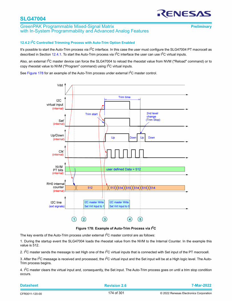
Datasheet 7-Mar-2022
CFR0011-120-00
Revision 2.6
174 of 301 © 2022 Renesas Electronics Corporation
SLG47004
GreenPAK Programmable Mixed-Signal Matrix with In-System Programmability and Advanced Analog Features
Preliminary
12.4.2 I2C Controlled Trimming Process with Auto-Trim Option Enabled
It's possible to start the Auto-Trim process via I2C interface. In this case the user must configure the SLG47004 PT macrocell as
described in Section 12.4.1. To start the Auto-Trim process via I2C interface the user can use I2C virtual inputs.
Also, an external I2C master device can force the SLG47004 to reload the rheostat value from NVM ("Reload" command) or to
copy rheostat value to NVM ("Program" command) using I2C virtual inputs.
See Figure 178 for an example of the Auto-Trim process under external I2C master control.
The key events of the Auto-Trim process under external I2C master control are as follows:
1. During the startup event the SLG47004 loads the rheostat value from the NVM to the Internal Counter. In the example thisvalue is 512.
2. I2C master sends the message to set High one of the I2C virtual inputs that is connected with Set input of the PT macrocell.
3. After the I2C message is received and processed, the I2C virtual input and the Set input will be at a High logic level. The Auto-Trim process begins.
4. I2C master clears the virtual input and, consequently, the Set input. The Auto-Trim process goes on until a trim stop conditionoccurs.
Figure 178: Example of Auto-Trim Process via I2C
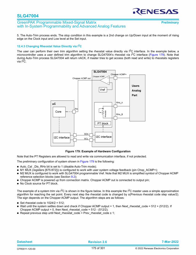
Datasheet 7-Mar-2022
CFR0011-120-00
Revision 2.6
175 of 301 © 2022 Renesas Electronics Corporation
SLG47004
GreenPAK Programmable Mixed-Signal Matrix with In-System Programmability and Advanced Analog Features
Preliminary
5. The Auto-Trim process ends. The stop condition in this example is a 2nd change on Up/Down input at the moment of risingedge on the Clock input and Low level at the Set input.
12.4.3 Changing Rheostat Value Directly via I2C
The user can perform their own trim algorithm setting the rheostat value directly via I2C interface. In the example below, amicrocontroller uses a user defined trim algorithm to change SLG47004‘s rheostat via I2C interface (Figure 179). Note thatduring Auto-Trim process SLG47004 will return nACK, if master tries to get access (both read and write) to rheostats registersvia I2C.
Note that the PT Registers are allowed to read and write via communication interface, if not protected.
The preliminary configuration of system shown in Figure 179 is the following:
Auto_Cal _Dis_RHx bit is set to 1 (disable Auto-Trim mode); M1 MUX (registers [875:872])) is configured to work with user system voltage feedback (pin Chop_ACMP+); M2 MUX is configured to work with SLG47004 programmable Vref. Note that M2 MUX is simplified symbol of Chopper ACMP
reference selection blocks (see Section 9.2); Chopper ACMP is powered up from connection matrix. Chopper ACMP out is connected to output pin; No Clock source for PT block.
The example of a system trim via I2C is shown in the figure below. In this example the I2C master uses a simple approximationalgorithm for reaching the set point. Every next step the rheostat code is changed by ±(Previous rheostat code step value/2).The sign depends on the Chopper ACMP output. The algorithm steps are as follows:
Set rheostat code to 1024/2 = 512; Wait until the system settles down and check if Chopper ACMP output = 1, then Next_rheostat_code = 512 + (512/2). If
Chopper ACMP output = 0, then Next_rheostat_code = 512 - (512/2); Repeat previous step until Next_rheostat_code = Prev_rheostat_code ± 1;
Figure 179: Example of Hardware Configuration

Datasheet 7-Mar-2022
CFR0011-120-00
Revision 2.6
176 of 301 © 2022 Renesas Electronics Corporation
SLG47004
GreenPAK Programmable Mixed-Signal Matrix with In-System Programmability and Advanced Analog Features
Preliminary
The key events of a user specific trimming process under I2C master control are as follows:
1. During the startup event the SLG47004 loads the rheostat value from NVM to Internal Counter. In the example this value is512.
2. I2C master writes a new value to the Rheostat’s Internal Counter according to Chopper ACMP output. Note that the minimumtime for changing the rheostat code depends on the time response of the user system.
3. After the trim process is completed, the I2C master sets the I2C virtual input to logic “1”. This input is connected to the"Reload" signal of the PT macrocell. The rising edge on this input starts the NVM self-programming routine.
4. The I2C master clears the I2C virtual input.
Additionally, the I2C Master macrocell can use internal resources such as an ADC to read the system data, find the error, and
then adjust the Rheostat value. Also, it is possible to change the Rheostat value for different conditions. For example, the I2CMaster macrocell can change the Rheostat value based on the temperature change to reduce the system error.
12.5 USING CHOPPER ACMP
When the Auto-Trim Function is disabled, the Chopper comparator can be used as a standalone analog comparator. Inputs ofthe Chopper ACMP are selected by the M1 and M2 analog MUXs. Output of the Chopper ACMP can be optionally inverted byregister [882]. This comparator output is the input [55] of the connection matrix. In case of a disabled Auto-Trim Function, thepower up source for the Chopper ACMP comes from connection matrix. Please refer to Section 9 for more details.
Figure 180: Example of User Specific Trimming Process under I2C Master Control

Datasheet 7-Mar-2022
CFR0011-120-00
Revision 2.6
177 of 301 © 2022 Renesas Electronics Corporation
SLG47004
GreenPAK Programmable Mixed-Signal Matrix with In-System Programmability and Advanced Analog Features
Preliminary
Figure 181: DNL vs. Digital Code, Rheostat Mode (VAB = 1 V) at T = 25 °C
Figure 182: INL vs. Digital Code, Rheostat Mode (VAB = 1 V) at T = 25 °C
-0.15
-0.1
-0.05
0
0.05
0.1
0.15
0.2
0 64 128 192 256 320 384 448 512 576 640 704 768 832 896 960 1024
DN
L (L
SB
)
Code (Decimal)
VDD = 2.4 V
VDD = 5.5 V
-0.2
-0.1
0
0.1
0.2
0.3
0.4
0.5
0.6
0.7
0.8
0 64 128 192 256 320 384 448 512 576 640 704 768 832 896 960 1024
INL
(LS
B)
Code (Decimal)
VDD = 2.4 V
VDD = 5.5 V

Datasheet 7-Mar-2022
CFR0011-120-00
Revision 2.6
178 of 301 © 2022 Renesas Electronics Corporation
SLG47004
GreenPAK Programmable Mixed-Signal Matrix with In-System Programmability and Advanced Analog Features
Preliminary
Figure 183: DNL vs. Digital Code, Potentiometer Mode (VAB = 1 V) at T = 25 °C
Figure 184: INL vs. Digital Code, Potentiometer Mode (VAB = 1 V) at T = 25 °C
-0.15
-0.1
-0.05
0
0.05
0.1
0.15
0.2
0 64 128 192 256 320 384 448 512 576 640 704 768 832 896 960 1024
DN
L (L
SB
)
Code (Decimal)
VDD = 2.4 V
VDD = 5.5 V
0
0.1
0.2
0.3
0.4
0.5
0.6
0.7
0.8
0.9
1
0 64 128 192 256 320 384 448 512 576 640 704 768 832 896 960 1024
INL
(LS
B)
Code (Decimal)
VDD = 2.4 V
VDD = 5.5 V

Datasheet 7-Mar-2022
CFR0011-120-00
Revision 2.6
179 of 301 © 2022 Renesas Electronics Corporation
SLG47004
GreenPAK Programmable Mixed-Signal Matrix with In-System Programmability and Advanced Analog Features
Preliminary
Figure 185: (ΔRAB/RAB)/ΔTA Rheostat Mode Tempco
Figure 186: RHx Zero Scale Error vs. Temperature (VIN = 1 V)
0
50
100
150
200
250
300
350
400
450
500
550
600
0 64 128 192 256 320 384 448 512 576 640 704 768 832 896 960 1024
Rh
eo
sta
t M
od
e T
em
pC
o (
pp
m/°
C)
Code (Decimal)
0
0.1
0.2
0.3
0.4
0.5
0.6
0.7
0.8
0.9
1
-40
-30
-20
-10 0
10
20
30
40
50
60
70
80
Ze
ro-S
cale
Err
or
(LS
B)
T (°C)
VDD = 5.5 V
VDD = 2.4 V

Datasheet 7-Mar-2022
CFR0011-120-00
Revision 2.6
180 of 301 © 2022 Renesas Electronics Corporation
SLG47004
GreenPAK Programmable Mixed-Signal Matrix with In-System Programmability and Advanced Analog Features
Preliminary
Figure 187: Transition Glitch in Worst Case (Code = 511 to Code = 512)
Figure 188: Gain vs. Frequency (Code = 512) at T = 25 °C, VDDA = 5 V
Vo
lta
ge
(0
.2 V
/div
)
Time (50 μs/div)
-50
-40
-30
-20
-10
0
10
10 100 1 000 10 000 100 000 1 000 000 10 000 000
Ga
in (
dB
)
f (Hz)
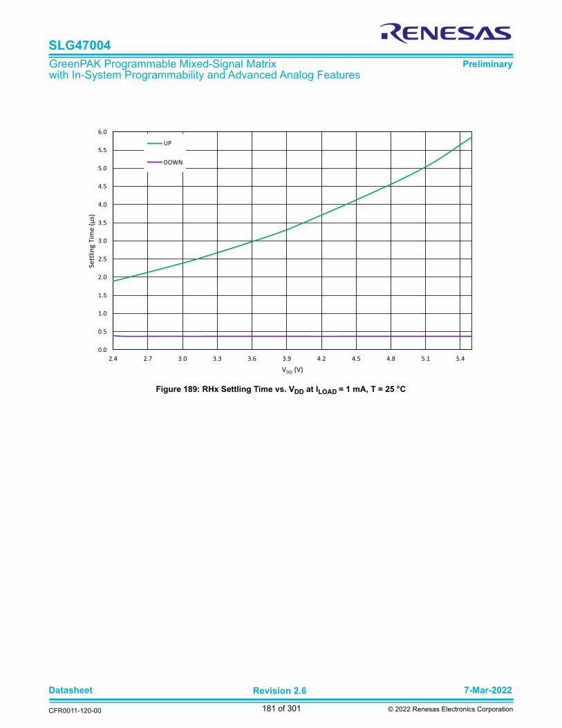
Datasheet 7-Mar-2022
CFR0011-120-00
Revision 2.6
181 of 301 © 2022 Renesas Electronics Corporation
SLG47004
GreenPAK Programmable Mixed-Signal Matrix with In-System Programmability and Advanced Analog Features
Preliminary
Figure 189: RHx Settling Time vs. VDD at ILOAD = 1 mA, T = 25 °C
0.0
0.5
1.0
1.5
2.0
2.5
3.0
3.5
4.0
4.5
5.0
5.5
6.0
2.4 2.7 3.0 3.3 3.6 3.9 4.2 4.5 4.8 5.1 5.4
Se
ttli
ng
Tim
e (
μs)
VDD (V)
UP
DOWN

Datasheet 7-Mar-2022
CFR0011-120-00
Revision 2.6
182 of 301 © 2022 Renesas Electronics Corporation
SLG47004
GreenPAK Programmable Mixed-Signal Matrix with In-System Programmability and Advanced Analog Features
Preliminary
13 Programmable Delay/Edge Detector
The SLG47004 has a programmable time delay logic cell available, that can generate a delay that is selectable from one of fourtimings (time 2) configured in the GreenPAK Designer. The programmable time delay cell can generate one of four different delaypatterns, rising edge detection, falling edge detection, both edge detection, and both edge delay. These four patterns can befurther modified with the addition of delayed edge detection, which adds an extra unit of delay, as well as glitch rejection duringthe delay period. See Figure 191 for further information.
Note: The input signal must be longer than the delay, otherwise it will be filtered out.
13.1 PROGRAMMABLE DELAY TIMING DIAGRAM - EDGE DETECTOR OUTPUT
Please refer to Table 13.
Figure 190: Programmable Delay
Figure 191: Edge Detector Output
Programmable Delay OUTIN
registers [865:864]
From Connection Matrix Output [58]To Connection
Matrix Input [30]
registers [867:866]Edge Mode SelectionDelay Value Selection
time1
Edge Detector Output
IN
Rising Edge Detector
Falling Edge Detector
Both Edge Detector
Both Edge Delay
time1
time1 is a fixed value time2 delay value is selected via register
time2 time2
width width

Datasheet 7-Mar-2022
CFR0011-120-00
Revision 2.6
183 of 301 © 2022 Renesas Electronics Corporation
SLG47004
GreenPAK Programmable Mixed-Signal Matrix with In-System Programmability and Advanced Analog Features
Preliminary
14 Additional Logic Function. Deglitch Filter
The SLG47004 has one Deglitch Filter macrocell with inverter function that is connected directly to the Connection Matrix inputsand outputs. In addition, this macrocell can be configured as an Edge Detector, with the following settings:
Rising Edge Detector Falling Edge Detector Both Edge Detector Both Edge Delay
Figure 192: Deglitch Filter or Edge Detector
From Connection MatrixOutput [59]
To Connection Matrix Input [31]
Filter
register [868]
C
R
register [869]
Edge Detector
Logic
registers [871:870]
0
1
0
1

Datasheet 7-Mar-2022
CFR0011-120-00
Revision 2.6
184 of 301 © 2022 Renesas Electronics Corporation
SLG47004
GreenPAK Programmable Mixed-Signal Matrix with In-System Programmability and Advanced Analog Features
Preliminary
15 Voltage Reference
15.1 VOLTAGE REFERENCE OVERVIEW
The SLG47004 has a Voltage Reference (Vref) Macrocell to provide reference to analog comparators and operational amplifiers.The macrocell also has the option to output reference voltages on external pins (see Table 1). Vref0 and Vref1 share output bufferswith Temperature sensor. Note that user can use any of output buffers, but Temperature sensor is calibrated for Vref1 outputbuffer. See Table 59 for the available selections for each analog comparator. Also, see Figure 193, Figure 194, and Figure 195,which show the reference output structure.
Also there is a high drive voltage reference macrocell called HD Buffer. The purpose of this macrocell is to provide stable voltageto the relatively high-power load (Please refer to the Table 20). HD Buffer has shared voltage reference source with the Op Amp0Vref. User can select output voltage in the range from VDD/64 to VDD with a step VDD/64, or output voltage in a range from 32 mVto 2.048 V with a step 32 mV (see Figure 195).
Note that Chopper ACMP will automatically enable HD Buffer if HD Buffer is selected as a source for Chopper ACMP In-signal(register 946 = 0) and Chopper ACMP is powered up.
15.2 VREF SELECTION TABLE
Table 59: Vref Selection Table
SEL[5:0] Vref SEL[5:0] Vref
0 0.032 33 1.088
1 0.064 34 1.12
2 0.096 35 1.152
3 0.128 36 1.184
4 0.16 37 1.216
5 0.192 38 1.248
6 0.224 39 1.28
7 0.256 40 1.312
8 0.288 41 1.344
9 0.32 42 1.376
10 0.352 43 1.408
11 0.384 44 1.44
12 0.416 45 1.472
13 0.448 46 1.504
14 0.48 47 1.536
15 0.512 48 1.568
16 0.544 49 1.6
17 0.576 50 1.632
18 0.608 51 1.664
19 0.64 52 1.696
20 0.672 53 1.728
21 0.704 54 1.76
22 0.736 55 1.792
23 0.768 56 1.824
24 0.8 57 1.856
25 0.832 58 1.888
26 0.864 59 1.92
27 0.896 60 1.952
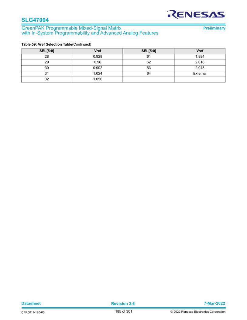
Datasheet 7-Mar-2022
CFR0011-120-00
Revision 2.6
185 of 301 © 2022 Renesas Electronics Corporation
SLG47004
GreenPAK Programmable Mixed-Signal Matrix with In-System Programmability and Advanced Analog Features
Preliminary
28 0.928 61 1.984
29 0.96 62 2.016
30 0.992 63 2.048
31 1.024 64 External
32 1.056
Table 59: Vref Selection Table(Continued)
SEL[5:0] Vref SEL[5:0] Vref
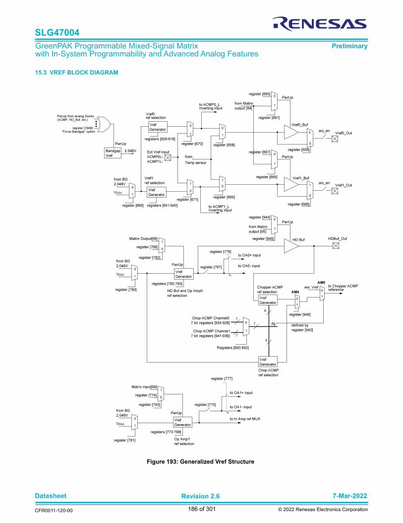
Datasheet 7-Mar-2022
CFR0011-120-00
Revision 2.6
186 of 301 © 2022 Renesas Electronics Corporation
SLG47004
GreenPAK Programmable Mixed-Signal Matrix with In-System Programmability and Advanced Analog Features
Preliminary
15.3 VREF BLOCK DIAGRAM
Figure 193: Generalized Vref Structure

Datasheet 7-Mar-2022
CFR0011-120-00
Revision 2.6
187 of 301 © 2022 Renesas Electronics Corporation
SLG47004
GreenPAK Programmable Mixed-Signal Matrix with In-System Programmability and Advanced Analog Features
Preliminary
Figure 194: ACMP0L, ACMP1L Voltage Reference Block Diagram

Datasheet 7-Mar-2022
CFR0011-120-00
Revision 2.6
188 of 301 © 2022 Renesas Electronics Corporation
SLG47004
GreenPAK Programmable Mixed-Signal Matrix with In-System Programmability and Advanced Analog Features
Preliminary
Figure 195: HD Buffer and Chopper ACMP Reference Block Diagram

Datasheet 7-Mar-2022
CFR0011-120-00
Revision 2.6
189 of 301 © 2022 Renesas Electronics Corporation
SLG47004
GreenPAK Programmable Mixed-Signal Matrix with In-System Programmability and Advanced Analog Features
Preliminary
Figure 196: Operational Amplifiers Voltage Reference Block Diagram

Datasheet 7-Mar-2022
CFR0011-120-00
Revision 2.6
190 of 301 © 2022 Renesas Electronics Corporation
SLG47004
GreenPAK Programmable Mixed-Signal Matrix with In-System Programmability and Advanced Analog Features
Preliminary
15.4 VOLTAGE REFERENCE TYPICAL PERFORMANCE
r.
Figure 197: Typical Load Regulation, Vref = 320 mV, T = -40 °C to +85 °C, Buffer - Enable
Figure 198: Typical Load Regulation, Vref = 640 mV, T = -40 °C to +85 °C, Buffer - Enable
0
50
100
150
200
250
300
350
0 1 2 3 4 5
VR
EF
OU
T,
mV
I, mA
VDD = 5 V
VDD = 3.3 V
VDD = 2.5 V
0
100
200
300
400
500
600
700
0 1 2 3 4 5
VR
EF
OU
T,
mV
I, mA
VDD = 5 V
VDD = 3.3 V
VDD = 2.5 V

Datasheet 7-Mar-2022
CFR0011-120-00
Revision 2.6
191 of 301 © 2022 Renesas Electronics Corporation
SLG47004
GreenPAK Programmable Mixed-Signal Matrix with In-System Programmability and Advanced Analog Features
Preliminary
Figure 199: Typical Load Regulation, Vref = 1280 mV, T = -40 °C to +85 °C, Buffer - Enable
Figure 200: Typical Load Regulation, Vref = 2048 mV, T = -40 °C to +85 °C, Buffer - Enable
0
200
400
600
800
1000
1200
1400
0 1 2 3 4 5
VR
EF
OU
T,
mV
I, mA
VDD = 5 V
VDD = 3.3 V
VDD = 2.5 V
0
300
600
900
1200
1500
1800
2100
0 1 2 3 4 5
VR
EF
OU
T,
mV
I, mA
VDD = 5 V
VDD = 3.3 V
VDD = 2.5 V
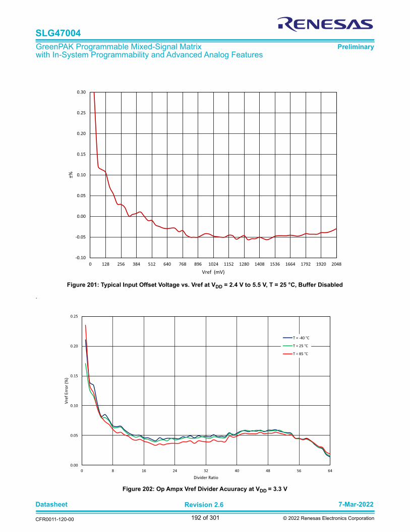
Datasheet 7-Mar-2022
CFR0011-120-00
Revision 2.6
192 of 301 © 2022 Renesas Electronics Corporation
SLG47004
GreenPAK Programmable Mixed-Signal Matrix with In-System Programmability and Advanced Analog Features
Preliminary
.
Figure 201: Typical Input Offset Voltage vs. Vref at VDD = 2.4 V to 5.5 V, T = 25 °C, Buffer Disabled
Figure 202: Op Ampx Vref Divider Acuuracy at VDD = 3.3 V
-0.10
-0.05
0.00
0.05
0.10
0.15
0.20
0.25
0.30
0 128 256 384 512 640 768 896 1024 1152 1280 1408 1536 1664 1792 1920 2048
±%
Vref (mV)
0.00
0.05
0.10
0.15
0.20
0.25
0 8 16 24 32 40 48 56 64
Vre
f E
rro
r (%
)
Divider Ratio
T = -40 °C
T = 25 °C
T = 85 °C
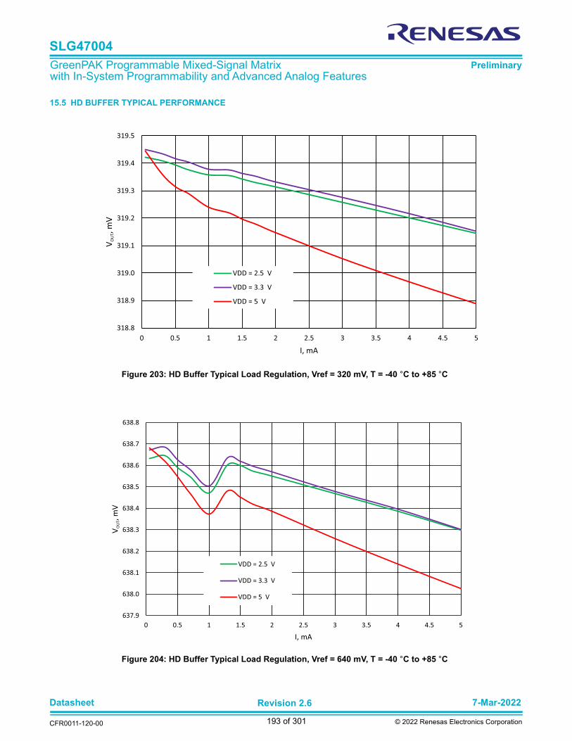
Datasheet 7-Mar-2022
CFR0011-120-00
Revision 2.6
193 of 301 © 2022 Renesas Electronics Corporation
SLG47004
GreenPAK Programmable Mixed-Signal Matrix with In-System Programmability and Advanced Analog Features
Preliminary
15.5 HD BUFFER TYPICAL PERFORMANCE
Figure 203: HD Buffer Typical Load Regulation, Vref = 320 mV, T = -40 °C to +85 °C
Figure 204: HD Buffer Typical Load Regulation, Vref = 640 mV, T = -40 °C to +85 °C
318.8
318.9
319.0
319.1
319.2
319.3
319.4
319.5
0 0.5 1 1.5 2 2.5 3 3.5 4 4.5 5
VO
UT,
mV
I, mA
VDD = 2.5 V
VDD = 3.3 V
VDD = 5 V
637.9
638.0
638.1
638.2
638.3
638.4
638.5
638.6
638.7
638.8
0 0.5 1 1.5 2 2.5 3 3.5 4 4.5 5
VO
UT,
mV
I, mA
VDD = 2.5 V
VDD = 3.3 V
VDD = 5 V

Datasheet 7-Mar-2022
CFR0011-120-00
Revision 2.6
194 of 301 © 2022 Renesas Electronics Corporation
SLG47004
GreenPAK Programmable Mixed-Signal Matrix with In-System Programmability and Advanced Analog Features
Preliminary
Figure 205: HD Buffer Typical Load Regulation, Vref = 1280 mV, T = -40 °C to +85 °C
Figure 206: HD Buffer Typical Load Regulation, Vref = 2048 mV, T = -40 °C to +85 °C
1276.2
1276.3
1276.4
1276.5
1276.6
1276.7
1276.8
1276.9
1277.0
1277.1
1277.2
0 0.5 1 1.5 2 2.5 3 3.5 4 4.5 5
VO
UT,
mV
I, mA
VDD = 2.5 V
VDD = 3.3 V
VDD = 5 V
2042.9
2043.0
2043.1
2043.2
2043.3
2043.4
2043.5
2043.6
2043.7
2043.8
2043.9
2044.0
0 0.5 1 1.5 2 2.5 3 3.5 4 4.5 5
VO
UT,
mV
I, mA
VDD = 2.5 V
VDD = 3.3 V
VDD = 5 V

Datasheet 7-Mar-2022
CFR0011-120-00
Revision 2.6
195 of 301 © 2022 Renesas Electronics Corporation
SLG47004
GreenPAK Programmable Mixed-Signal Matrix with In-System Programmability and Advanced Analog Features
Preliminary
Figure 207: HD Buffer Typical Line Regulation, ILOAD = 5 mA
Figure 208: HD Buffer Offset vs. VDD
2041
2042
2043
2044
2045
2046
2047
2.4 2.7 3 3.3 3.6 3.9 4.2 4.5 4.8 5.1 5.4
VO
UT
(mV
)
VDD (V)
T = 25 °C
T = 85 °C
T = -40 °C
0
50
100
150
200
250
300
2.4 2.7 3 3.3 3.6 3.9 4.2 4.5 4.8 5.1 5.4
Off
set
(μV
)
VDD (V)
T = 85 °C
T = 25 °C
T = -40 °C
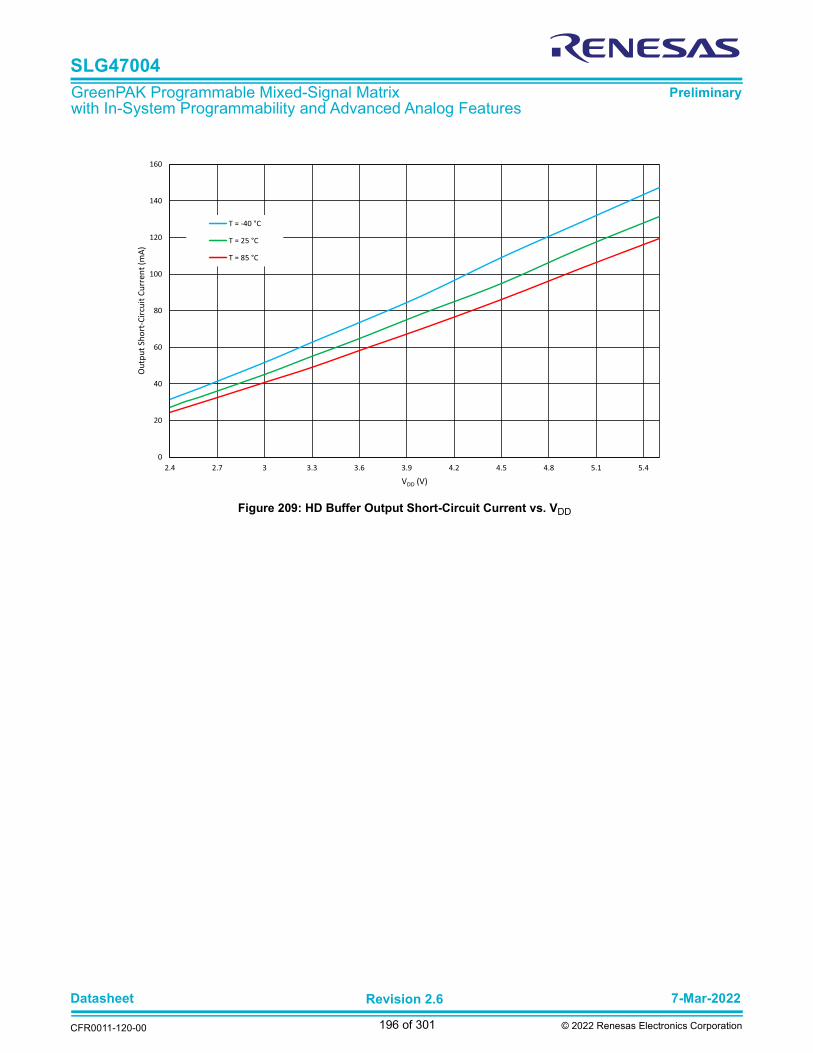
Datasheet 7-Mar-2022
CFR0011-120-00
Revision 2.6
196 of 301 © 2022 Renesas Electronics Corporation
SLG47004
GreenPAK Programmable Mixed-Signal Matrix with In-System Programmability and Advanced Analog Features
Preliminary
Figure 209: HD Buffer Output Short-Circuit Current vs. VDD
0
20
40
60
80
100
120
140
160
2.4 2.7 3 3.3 3.6 3.9 4.2 4.5 4.8 5.1 5.4
Ou
tpu
t S
ho
rt-C
ircu
it C
urr
en
t (m
A)
VDD (V)
T = -40 °C
T = 25 °C
T = 85 °C

Datasheet 7-Mar-2022
CFR0011-120-00
Revision 2.6
197 of 301 © 2022 Renesas Electronics Corporation
SLG47004
GreenPAK Programmable Mixed-Signal Matrix with In-System Programmability and Advanced Analog Features
Preliminary
16 Clocking
16.1 OSC GENERAL DESCRIPTION
The SLG47004 has three internal oscillators to support a variety of applications:
Oscillator0 (2.048 kHz) Oscillator1 (2.048 MHz) Oscillator2 (25 MHz)
There are two divider stages for each oscillator that give the user flexibility for introducing clock signals to connection matrix, aswell as various other Macrocells. The pre-divider (first stage) for Oscillator allows the selection of /1, /2, /4, or /8 to divide downfrequency from the fundamental. The second stage divider has an input of frequency from the pre-divider, and outputs one ofeight different frequencies divided by /1, /2, /3, /4, /8, /12, /24, or /64 on Connection Matrix Input lines [52], [53], and [54]. Pleasesee Figure 213 for more details on the SLG47004 clock scheme.
Oscillator2 (25 MHz) has an additional function of 100 ns delayed startup, which can be enabled/disabled by register [713]. Thisfunction is recommended to use when analog blocks are used along with the Oscillator.
The Matrix Power-down/Force On function allows switching off or force on the oscillator using an external pin. The Matrix Power-down/Force On (Connection Matrix Output [91], [92], [93]) signal has the highest priority. The OSC operates according to theTable 60
It is highly recommended to force the bandgap on when OSC1 or OSC2 are used in the project.
Table 60: Oscillator Operation Mode Configuration Settings
PORExternal
ClockSelection
Signal From Connection
Matrix
Register: Power-Down or Force On by Matrix In-
put
Register: Auto Power-On or Force
On
OSC Enable
Signal from
CNT/DLY
Macrocells
OSC
Operation
Mode
0 X X X X X OFF
1 1 X X XX Internal OSC
is OFF,logic is ON
1 0 1 0 X X OFF
1 0 1 1 X X ON
1 0 0 X 1 X ON
1 0 0 X 0 CNT/DLYrequires OSC
ON
1 0 0 X 0CNT/DLY does not
require OSC
OFF
Note 1 The OSC will run only when any macrocell that uses OSC is powered on.

Datasheet 7-Mar-2022
CFR0011-120-00
Revision 2.6
198 of 301 © 2022 Renesas Electronics Corporation
SLG47004
GreenPAK Programmable Mixed-Signal Matrix with In-System Programmability and Advanced Analog Features
Preliminary
16.2 OSCILLATOR0 (2.048 KHZ)
Figure 210: Oscillator0 Block Diagram
OSC0(2.048 kHz)
Ext. CLK Sel register [722]
/ 2
/ 3
/ 4
/ 8
/ 12
/ 24
/ 64
0
1
2
3
4
5
6
7
To Connection MatrixInput [52]
registers [728:726]
DIV /1 /2 /4 /8
registers [725:724]
Pre-divider
Second StageDivider
0
1
From Connection Matrix Output [91]
PD/FORCE ON
Auto Power-On0
1Force Power-On
OSC Power Moderegister [720]
2.048 kHz Pre-divided Clock
Ext. Clock
OUT
Power-down/Force On Matrix Output control register [721]
To Connection MatrixInput [58]
registers [733:731]
OUT1
OUT0

Datasheet 7-Mar-2022
CFR0011-120-00
Revision 2.6
199 of 301 © 2022 Renesas Electronics Corporation
SLG47004
GreenPAK Programmable Mixed-Signal Matrix with In-System Programmability and Advanced Analog Features
Preliminary
16.3 OSCILLATOR1 (2.048 MHZ)
Figure 211: Oscillator1 Block Diagram
OSC1(2.048 MHz)
Ext. CLK Sel register [690]
/ 2
/ 3
/ 4
/ 8
/ 12
/ 24
/ 64
0
1
2
3
4
5
6
7
To Connection MatrixInput [53]
registers [695:693]
DIV /1 /2 /4 /8
registers [692:691]
Pre-divider
Second StageDivider
0
1
From Connection Matrix Output [92]
PD/FORCE ON
Auto Power-On0
1Force Power-On
OSC Power Moderegister [688]
2.048 MHz Pre-divided Clock
Ext. Clock
OUT
Power-down/Force On Matrix Output control register [689]
To Connection MatrixInput [59]
registers [703:701]
OUT1
OUT0

Datasheet 7-Mar-2022
CFR0011-120-00
Revision 2.6
200 of 301 © 2022 Renesas Electronics Corporation
SLG47004
GreenPAK Programmable Mixed-Signal Matrix with In-System Programmability and Advanced Analog Features
Preliminary
16.4 OSCILLATOR2 (25 MHZ)
16.5 CNT/DLY CLOCK SCHEME
Each CNT/DLY within Multi-Function macrocell has its own additional clock divider connected to oscillators pre-divider. Availabledividers are:
OSC0/1, OSC0/8, OSC0/64, OSC0/512, OSC0/4096, OSC0/32768, OSC0/262144 OSC1/1, OSC1/8, OSC1/64, OSC1/512 OSC2/1, OSC2/4
Figure 212: Oscillator2 Block Diagram
OSC2(25 MHz)
Ext. CLK Sel [706]
/ 2
/ 3
/ 4
/ 8
/ 12
/ 24
/ 64
0
1
2
3
4
5
6
7
To Connection MatrixInput [54]
registers [712:710]
DIV /1 /2 /4 /8
registers [709:708]
Pre-divider
Second StageDivider
0
1
From Connection Matrix Output [93]
PD/FORCE ON
Auto Power-On0
1Force Power-On
OSC Power Moderegister [704]
25 MHz Pre-divided Clock
Ext. Clock
OUT
Power-down/Force On Matrix Output control register [705]
Startup delay
register [713]

Datasheet 7-Mar-2022
CFR0011-120-00
Revision 2.6
201 of 301 © 2022 Renesas Electronics Corporation
SLG47004
GreenPAK Programmable Mixed-Signal Matrix with In-System Programmability and Advanced Analog Features
Preliminary
16.6 EXTERNAL CLOCKING
The SLG47004 supports several ways to use an external, higher accuracy clock as a reference source for internal operations.
16.6.1 IO10 Source for Oscillator0 (2.048 kHz)
When register [722] is set to 1, an external clocking signal on IO0 will be routed in place of the internal oscillator derived 2.048 kHzclock source. See Figure 210. The high and low limits for frequency that can be selected are 0 MHz and 10 MHz.
16.6.2 IO1 Source for Oscillator1 (2.048 MHz)
When register [690] is set to 1, an external clocking signal on IO1 will be routed in place of the internal oscillator derived 2.048 MHzclock source. See Figure 211. The high and low limits for frequency that can be selected are 0 MHz and 10 MHz.
16.6.3 IO2 Source for Oscillator2 (25 MHz)
When register [706] is set to 1, an external clocking signal on IO2 will be routed in place of the internal oscillator derived 25 MHzclock source. See Figure 212. The external frequency range is 0 MHz to 20 MHz at VDD = 2.4 V, 0 MHz to 30 MHz at VDD = 3.3 V,0 MHz to 50 MHz at VDD = 5.0 V. When an external clock is selected for OSC2, the oscillator's output signal will be inverted withrespect to the IO2 input signal.
Figure 213: Clock Scheme
0123456789101112131415
CNT/DLY/ONESHOT/FREQ_DET/
DLY_EDGE_DET
CNT overflowDiv8
Div64
Div512
Div32768
Div4096
Div262144
Div8
Div64
Div512
Div425 MHz Pre-divided clock
2.048 MHz Pre-divided clock
2.048 kHz Pre-divided clock
CNT (x-1) overflow
from Connection Matrix Out(separate for each CNT/DLY macrocell)
[3:0]
CNT0/CNT1/CNT2/CNT3/CNT4/CNT5/CNT6/RH0 CLK/RH1 CLK
none

Datasheet 7-Mar-2022
CFR0011-120-00
Revision 2.6
202 of 301 © 2022 Renesas Electronics Corporation
SLG47004
GreenPAK Programmable Mixed-Signal Matrix with In-System Programmability and Advanced Analog Features
Preliminary
16.7 OSCILLATORS POWER-ON DELAY
Note 1 OSC power mode: “Auto Power-On”.
Note 2 “OSC enable” signal appears when any macrocell that uses OSC is powered on
Figure 214: Oscillator Startup Diagram
Figure 215: OSC0 Maximum Power-On Delay vs. VDD at T = 25 °C, OSC0 = 2.048 kHz
CLK
OSC enable Power-OnDelay
500
550
600
650
700
750
800
850
900
950
2.4 2.7 3 3.3 3.6 3.9 4.2 4.5 4.8 5.1 5.4
Po
we
r-O
n D
ela
y (
μs)
VDD (V)

Datasheet 7-Mar-2022
CFR0011-120-00
Revision 2.6
203 of 301 © 2022 Renesas Electronics Corporation
SLG47004
GreenPAK Programmable Mixed-Signal Matrix with In-System Programmability and Advanced Analog Features
Preliminary
Figure 216: OSC1 Oscillator Maximum Power-On Delay vs. VDD at T = 25 °C, OSC1 = 2.048 MHz
Figure 217: OSC2 Maximum Power-On Delay vs. VDD at T = 25 °C, OSC2 = 25 MHz
400
420
440
460
480
500
520
540
560
2.4 2.7 3 3.3 3.6 3.9 4.2 4.5 4.8 5.1 5.4
Po
we
r-O
n D
ela
y (
ns)
VDD (V)
0
20
40
60
80
100
120
140
160
2.4 2.7 3 3.3 3.6 3.9 4.2 4.5 4.8 5.1 5.4
Po
we
r-O
n D
ela
y (
ns)
VDD (V)

Datasheet 7-Mar-2022
CFR0011-120-00
Revision 2.6
204 of 301 © 2022 Renesas Electronics Corporation
SLG47004
GreenPAK Programmable Mixed-Signal Matrix with In-System Programmability and Advanced Analog Features
Preliminary
16.8 OSCILLATORS ACCURACY
Note: OSC power setting: Force Power-On; Clock to matrix input - enable; Bandgap: turn on by register - enable.
Figure 218: OSC0 Frequency vs. Temperature, OSC0 = 2.048 kHz
Figure 219: OSC1 Frequency vs. Temperature, OSC1 = 2.048 MHz
1.9
1.92
1.94
1.96
1.98
2
2.02
2.04
2.06
2.08
2.1
2.12
2.14
2.16
2.18
2.2-4
0
-30
-20
-10 0
10
20
30
40
50
60
70
80
f (k
Hz)
T (°C)
Fmax @ VDD = 2.5 V to 5 V
Ftyp @ VDD = 3.3 V
Fmin @ VDD = 2.5 V to 5 V
1.95
1.97
1.99
2.01
2.03
2.05
2.07
2.09
2.11
2.13
2.15
-40
-30
-20
-10 0
10
20
30
40
50
60
70
80
f (M
Hz)
T (°C)
Fmax @ VDD = 2.5 V to 5 V
Ftyp @ VDD = 3.3 V
Fmin @ VDD = 2.5 V to 5.5 V
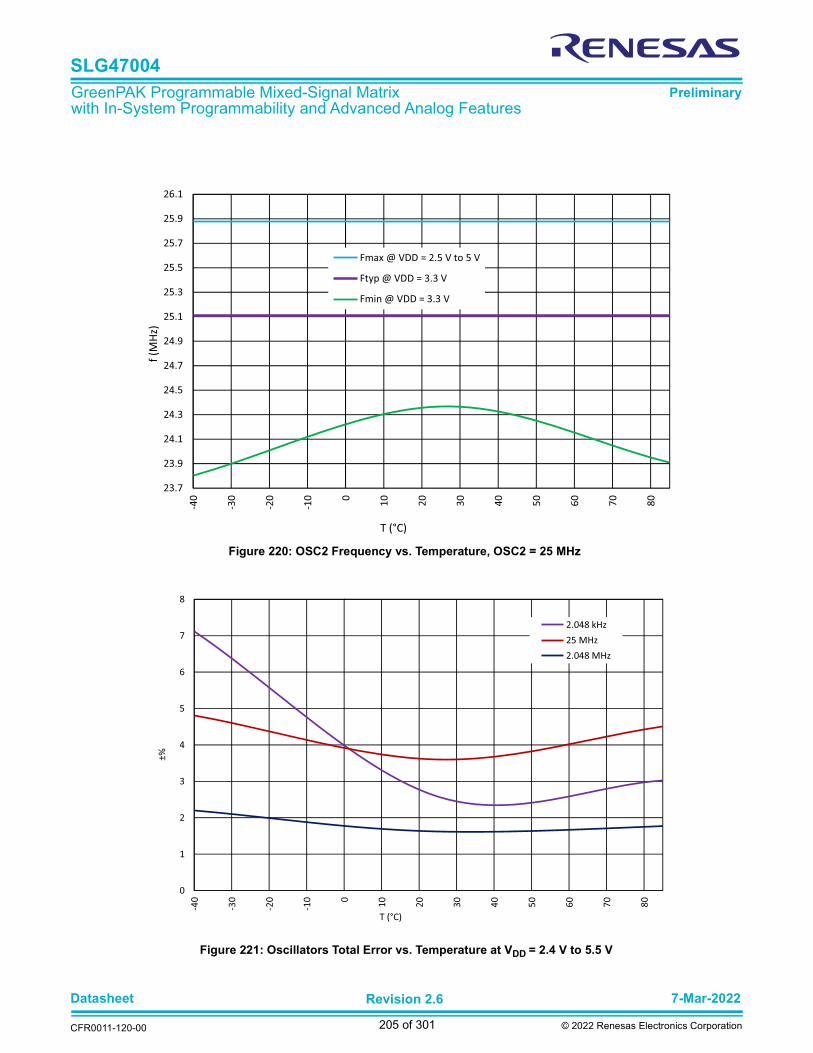
Datasheet 7-Mar-2022
CFR0011-120-00
Revision 2.6
205 of 301 © 2022 Renesas Electronics Corporation
SLG47004
GreenPAK Programmable Mixed-Signal Matrix with In-System Programmability and Advanced Analog Features
Preliminary
Figure 220: OSC2 Frequency vs. Temperature, OSC2 = 25 MHz
Figure 221: Oscillators Total Error vs. Temperature at VDD = 2.4 V to 5.5 V
23.7
23.9
24.1
24.3
24.5
24.7
24.9
25.1
25.3
25.5
25.7
25.9
26.1-4
0
-30
-20
-10 0
10
20
30
40
50
60
70
80
f (M
Hz)
T (°C)
Fmax @ VDD = 2.5 V to 5 V
Ftyp @ VDD = 3.3 V
Fmin @ VDD = 3.3 V
0
1
2
3
4
5
6
7
8
-40
-30
-20
-10 0
10
20
30
40
50
60
70
80
±%
T (°C)
2.048 kHz
25 MHz
2.048 MHz

Datasheet 7-Mar-2022
CFR0011-120-00
Revision 2.6
206 of 301 © 2022 Renesas Electronics Corporation
SLG47004
GreenPAK Programmable Mixed-Signal Matrix with In-System Programmability and Advanced Analog Features
Preliminary
Note: For more information see Section 3.8.
16.9 OSCILLATORS SETTLING TIME
Figure 222: Oscillator0 Settling Time, VDD = 3.3 V, T = 25 °C, OSC0 = 2 kHz
Figure 223: Oscillator1 Settling Time, VDD = 3.3 V, T = 25 °C, OSC1 = 2 MHz
484
485
486
487
488
0 1 2 3 4
Tim
e (
μs)
Period
450
460
470
480
490
500
510
0 1 2 3 4 5 6
Tim
e (
ns)
Period

Datasheet 7-Mar-2022
CFR0011-120-00
Revision 2.6
207 of 301 © 2022 Renesas Electronics Corporation
SLG47004
GreenPAK Programmable Mixed-Signal Matrix with In-System Programmability and Advanced Analog Features
Preliminary
Figure 224: Oscillator2 Settling Time, VDD = 3.3 V, T = 25 °C, OSC2 = 25 MHz (Normal Start)
Figure 225: Oscillator2 Settling Time, VDD = 3.3 V, T = 25 °C, OSC2 = 25 MHz (Start with Delay)
20
25
30
35
40
45
50
55
60
0 1 2 3 4 5 6 7 8 9 10 11
Tim
e (
ns)
Period
20
40
60
80
100
120
140
160
0 1 2 3 4 5 6 7 8
Tim
e (
ns)
Period
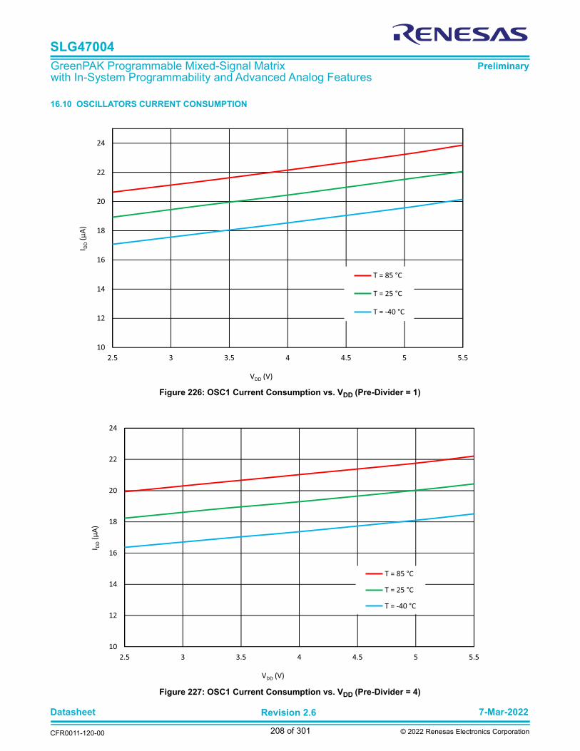
Datasheet 7-Mar-2022
CFR0011-120-00
Revision 2.6
208 of 301 © 2022 Renesas Electronics Corporation
SLG47004
GreenPAK Programmable Mixed-Signal Matrix with In-System Programmability and Advanced Analog Features
Preliminary
16.10 OSCILLATORS CURRENT CONSUMPTION
Figure 226: OSC1 Current Consumption vs. VDD (Pre-Divider = 1)
Figure 227: OSC1 Current Consumption vs. VDD (Pre-Divider = 4)
10
12
14
16
18
20
22
24
2.5 3 3.5 4 4.5 5 5.5
I DD
(μA
)
VDD (V)
T = 85 °C
T = 25 °C
T = -40 °C
10
12
14
16
18
20
22
24
2.5 3 3.5 4 4.5 5 5.5
I DD
(μA
)
VDD (V)
T = 85 °C
T = 25 °C
T = -40 °C
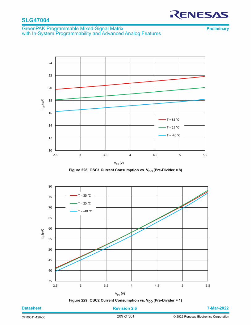
Datasheet 7-Mar-2022
CFR0011-120-00
Revision 2.6
209 of 301 © 2022 Renesas Electronics Corporation
SLG47004
GreenPAK Programmable Mixed-Signal Matrix with In-System Programmability and Advanced Analog Features
Preliminary
Figure 228: OSC1 Current Consumption vs. VDD (Pre-Divider = 8)
Figure 229: OSC2 Current Consumption vs. VDD (Pre-Divider = 1)
10
12
14
16
18
20
22
24
2.5 3 3.5 4 4.5 5 5.5
I DD
(μA
)
VDD (V)
T = 85 °C
T = 25 °C
T = -40 °C
35
40
45
50
55
60
65
70
75
80
2.5 3 3.5 4 4.5 5 5.5
I DD
(μA
)
VDD (V)
T = 85 °C
T = 25 °C
T = -40 °C
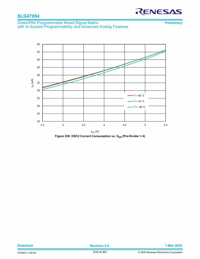
Datasheet 7-Mar-2022
CFR0011-120-00
Revision 2.6
210 of 301 © 2022 Renesas Electronics Corporation
SLG47004
GreenPAK Programmable Mixed-Signal Matrix with In-System Programmability and Advanced Analog Features
Preliminary
Figure 230: OSC2 Current Consumption vs. VDD (Pre-Divider = 4)
10
15
20
25
30
35
40
45
50
55
60
2.5 3 3.5 4 4.5 5 5.5
I DD
(μA
)
VDD (V)
T = 85 °C
T = 25 °C
T = -40 °C
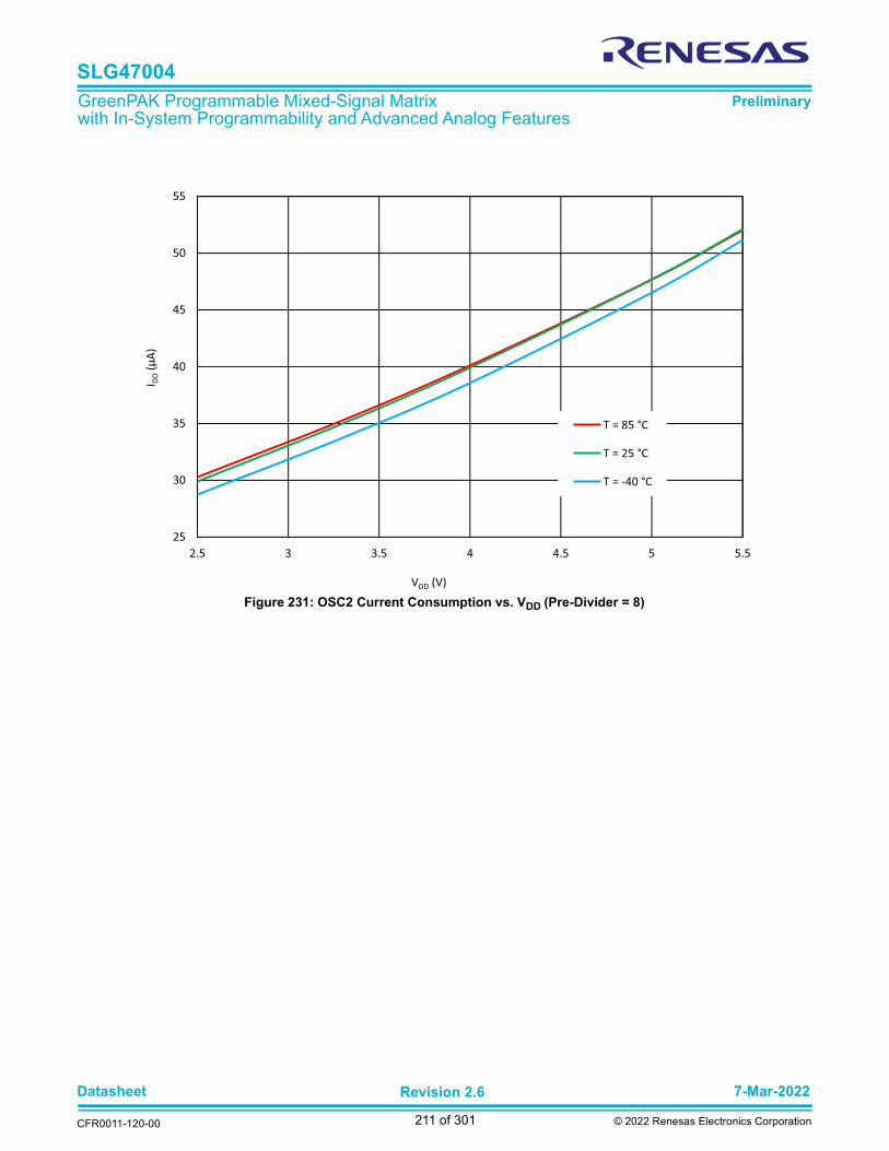
Datasheet 7-Mar-2022
CFR0011-120-00
Revision 2.6
211 of 301 © 2022 Renesas Electronics Corporation
SLG47004
GreenPAK Programmable Mixed-Signal Matrix with In-System Programmability and Advanced Analog Features
Preliminary
Figure 231: OSC2 Current Consumption vs. VDD (Pre-Divider = 8)
25
30
35
40
45
50
55
2.5 3 3.5 4 4.5 5 5.5
I DD
(μA
)
VDD (V)
T = 85 °C
T = 25 °C
T = -40 °C

Datasheet 7-Mar-2022
CFR0011-120-00
Revision 2.6
212 of 301 © 2022 Renesas Electronics Corporation
SLG47004
GreenPAK Programmable Mixed-Signal Matrix with In-System Programmability and Advanced Analog Features
Preliminary
17 Power-On Reset
The SLG47004 has a Power-On Reset (POR) macrocell to ensure correct device initialization and operation of all macrocells inthe device. The purpose of the POR circuit is to have consistent behavior and predictable results when the VDD power is firstramping to the device, and also while the VDD is falling during Power-down. To accomplish this goal, the POR drives a definedsequence of internal events that trigger changes to the states of different macrocells inside the device, and finally to the state ofthe IOs.
17.1 GENERAL OPERATION
The SLG47004 is guaranteed to be powered down and non-operational when the VDD voltage (voltage on PIN13) is less thanPower-Off Threshold (see in Table 6), but not less than -0.6 V. Another essential condition for the chip to be powered down is thatno voltage higher (Note) than the VDD voltage is applied to any other PIN. For example, if VDD voltage is 0.3 V, applying a voltagehigher than 0.3 V to any other PIN is incorrect, and can lead to incorrect or unexpected device behavior.
Note: There is a 0.6 V margin due to forward drop voltage of the ESD protection diodes.
To start the POR sequence in the SLG47004, the voltage applied on the VDD should be higher than the Power-On Threshold(Note). The full operational VDD range for the SLG47004 is 2.4 V to 5.5 V. This means that the VDD voltage must ramp up to theoperational voltage value, but the POR sequence will start earlier, as soon as the VDD voltage rises to the Power-On Threshold.After the POR sequence has started, the SLG47004 will have a typical Startup Time (see in Table 6) to go through all the stepsin the sequence, and will be ready and completely operational after the POR sequence is complete.
Note: The Power-On Threshold is defined in Table 6.
To power down the chip, the VDD voltage should be lower than the operational and to guarantee that chip is powered down, itshould be less than Power-Off Threshold.
All PINs are in high impedance state when the chip is powered down and while the POR sequence is taking place. The last stepin the POR sequence releases the IO structures from the high impedance state, at which time the device is operational. The pinconfiguration at this point in time is defined by the design programmed into the chip. Also, as it was mentioned before, the voltageon PINs can’t be bigger than the VDD, this rule also applies to the case when the chip is powered on.

Datasheet 7-Mar-2022
CFR0011-120-00
Revision 2.6
213 of 301 © 2022 Renesas Electronics Corporation
SLG47004
GreenPAK Programmable Mixed-Signal Matrix with In-System Programmability and Advanced Analog Features
Preliminary
17.2 POR SEQUENCE
The POR system generates a sequence of signals that enable certain macrocells. The sequence is shown in Figure 232.
As can be seen from Figure 232 after the VDD has started ramping up and crossed the Power-On Threshold, first, the on-chipNVM memory is reset. Next, the chip reads the data from NVM and transfers this information to a CMOS LATCH, that serves toconfigure each macrocell, and the Connection Matrix, which routes signals between macrocells. The third stage causes the resetof the input pins, and then enables them. At that time Digital Rheostats value is set to its default value. After that, the LUTs arereset and become active. After LUTs, the Delay cells, OSCs, DFFs, LATCHES, and Pipe Delay are initialized. Only after allmacrocells are initialized, internal POR signal (POR macrocell output) goes from LOW to HIGH (POR_OUT in Figure 232). Thelast portion of the device to be initialized is the output pins, which transition from high impedance to active at this point.
The typical time that takes to complete the POR sequence varies by device type in the GreenPAK family. It also depends on manyenvironmental factors, such as: slew rate, VDD value, temperature, and even will vary from chip to chip (process influence).
17.3 MACROCELLS OUTPUT STATES DURING POR SEQUENCE
To have a full picture of SLG47004 operation during powering and POR sequence refer to Figure 233, which describes themacrocell output states during the POR sequence.
First, before the NVM has been reset, all macrocells have their output set to logic LOW (except the output pins which are in highimpedance state). On the next step, some of the macrocells start initialization: input pins output state becomes LOW; DigitalRheostats value is set to its default value; LUTs also output LOW. After that input pins are enabled. Next, only LUTs are configured.Then, all other macrocells are initialized. After macrocells are initialized, internal POR matrix signal switches from LOW to HIGH.The last are output pins that become active and determined by the input signals.
Figure 232: POR Sequence
VDD
POR_NVM(reset for NVM)
NVM_ready_out
POR_GPI(reset for input enable,
Digital Rheostat (default value))
POR_LUT(reset for LUT/FILTER)
POR_CORE(reset for DLY/OSC/DFF
/LATCH/Pipe DLY/ACMP/Edge Detector in Filter)
POR_OUT(generate low to high to matrix)
POR_GPO(reset for output enable)
t
t
t
t
t
t
t
t

Datasheet 7-Mar-2022
CFR0011-120-00
Revision 2.6
214 of 301 © 2022 Renesas Electronics Corporation
SLG47004
GreenPAK Programmable Mixed-Signal Matrix with In-System Programmability and Advanced Analog Features
Preliminary
17.3.1 Initialization
All internal macrocells by default have initial low level. Starting from indicated power-up time of 1.63 V to 2.04 V, macrocells inSLG47004 are powered on while forced to the reset state. All outputs are in Hi-Z and chip starts loading data from NVM. Thenthe reset signal is released for internal macrocells and they start to initialize according to the following sequence:
1. Input pins, Pull-up/down, Digital Rheostats, Op Amps.
2. LUTs.
3. DFFs, Delays/Counters, Pipe Delay, OSCs, ACMPs.
4. POR output to matrix.
5. Output pin corresponds to the internal logic.
The Vref output pin driving signal can precede POR output signal going high by 3 µs to 5 µs. The POR signal going high indicatesthe mentioned power-up sequence is complete.
Note: The maximum voltage applied to any pin should not be higher than the VDD level. There are ESD Diodes between pin →
Figure 233: Internal Macrocell States During POR Sequence
Unpredictable
Unpredictable
Unpredictable
Unpredictable
Unpredictable
Unpredictable
Unpredictable
VDD
Input PIN _outto matrix
LUT/FILTER_outto matrix
Programmable Delay_outto matrix
DFF/LATCH/ACMP/EdgeDetector in Filter_out
to matrix
Delay_outto matrix
POR_outto matrix
Ext. GPO
VDD _outto matrix
Determined by Input signals
Determined by Input signalsStarts to detect input edges
Determined by Input signals
Determined by Input signalsStarts to detect input edges
Determined by input signals
Determined by External Signal
Guaranteed HIGH before POR_GPI
Determined by input signals OUT = IN without Delay
Determined by initial state
Determined by input signals OUT = IN without Delay
Tri-state
t
t
t
t
t
t
t
t
t
Output State Unpredictable
Hi-ZDigital Rheostats
Resistance Default Value from NVM
t

Datasheet 7-Mar-2022
CFR0011-120-00
Revision 2.6
215 of 301 © 2022 Renesas Electronics Corporation
SLG47004
GreenPAK Programmable Mixed-Signal Matrix with In-System Programmability and Advanced Analog Features
Preliminary
VDD and pin → GND on each pin. Exceeding VDD results in leakage current on the input pin, and VDD will be pulled up, followingthe voltage on the input pin.
17.3.2 Power-Down
During Power-down macrocells in SLG47004 are powered off after VDD falling down below Power-Off Threshold. Please note,that during a slow rampdown outputs can possibly switch state.
Figure 234: Power-Down
Not guaranteed output state
VDD (V)
Time
1.54 V
0.96 V
2 V
1 V1 V Vref Out Signal
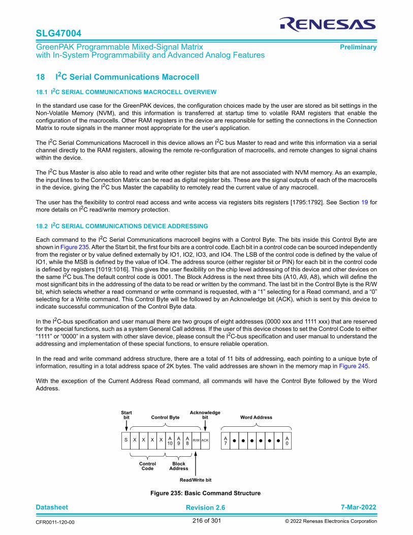
Datasheet 7-Mar-2022
CFR0011-120-00
Revision 2.6
216 of 301 © 2022 Renesas Electronics Corporation
SLG47004
GreenPAK Programmable Mixed-Signal Matrix with In-System Programmability and Advanced Analog Features
Preliminary
18 I2C Serial Communications Macrocell
18.1 I2C SERIAL COMMUNICATIONS MACROCELL OVERVIEW
In the standard use case for the GreenPAK devices, the configuration choices made by the user are stored as bit settings in theNon-Volatile Memory (NVM), and this information is transferred at startup time to volatile RAM registers that enable theconfiguration of the macrocells. Other RAM registers in the device are responsible for setting the connections in the ConnectionMatrix to route signals in the manner most appropriate for the user’s application.
The I2C Serial Communications Macrocell in this device allows an I2C bus Master to read and write this information via a serialchannel directly to the RAM registers, allowing the remote re-configuration of macrocells, and remote changes to signal chainswithin the device.
The I2C bus Master is also able to read and write other register bits that are not associated with NVM memory. As an example,the input lines to the Connection Matrix can be read as digital register bits. These are the signal outputs of each of the macrocellsin the device, giving the I2C bus Master the capability to remotely read the current value of any macrocell.
The user has the flexibility to control read access and write access via registers bits registers [1795:1792]. See Section 19 formore details on I2C read/write memory protection.
18.2 I2C SERIAL COMMUNICATIONS DEVICE ADDRESSING
Each command to the I2C Serial Communications macrocell begins with a Control Byte. The bits inside this Control Byte areshown in Figure 235. After the Start bit, the first four bits are a control code. Each bit in a control code can be sourced independentlyfrom the register or by value defined externally by IO1, IO2, IO3, and IO4. The LSB of the control code is defined by the value ofIO1, while the MSB is defined by the value of IO4. The address source (either register bit or PIN) for each bit in the control codeis defined by registers [1019:1016]. This gives the user flexibility on the chip level addressing of this device and other devices onthe same I2C bus.The default control code is 0001. The Block Address is the next three bits (A10, A9, A8), which will define themost significant bits in the addressing of the data to be read or written by the command. The last bit in the Control Byte is the R/Wbit, which selects whether a read command or write command is requested, with a “1” selecting for a Read command, and a “0”selecting for a Write command. This Control Byte will be followed by an Acknowledge bit (ACK), which is sent by this device toindicate successful communication of the Control Byte data.
In the I2C-bus specification and user manual there are two groups of eight addresses (0000 xxx and 1111 xxx) that are reservedfor the special functions, such as a system General Call address. If the user of this device choses to set the Control Code to either“1111” or “0000” in a system with other slave device, please consult the I2C-bus specification and user manual to understand theaddressing and implementation of these special functions, to ensure reliable operation.
In the read and write command address structure, there are a total of 11 bits of addressing, each pointing to a unique byte ofinformation, resulting in a total address space of 2K bytes. The valid addresses are shown in the memory map in Figure 245.
With the exception of the Current Address Read command, all commands will have the Control Byte followed by the WordAddress.
Figure 235: Basic Command Structure
X X X X A10
A9
A8
R/W A7
A0
Control Byte Word Address
Control Code
Block Address
Read/Write bit
S ACK
Acknowledgebit
Startbit

Datasheet 7-Mar-2022
CFR0011-120-00
Revision 2.6
217 of 301 © 2022 Renesas Electronics Corporation
SLG47004
GreenPAK Programmable Mixed-Signal Matrix with In-System Programmability and Advanced Analog Features
Preliminary
18.3 I2C SERIAL GENERAL TIMING
General timing characteristics for the I2C Serial Communications macrocell are shown in Figure 236. Timing specifications canbe found in the AC Characteristics, section 3.4.
18.4 I2C SERIAL COMMUNICATIONS COMMANDS
18.4.1 Byte Write Command
Following the Start condition from the Master, the Control Code [4 bits], the Block Address [3 bits], and the R/W bit (set to “0”) areplaced onto the I2C bus by the Master. After the SLG47004 sends an Acknowledge bit (ACK), the next byte transmitted by theMaster is the Word Address. The Block Address (A10, A9, A8), combined with the Word Address (A7 through A0), together setthe internal address pointer in the SLG47004, where the data byte is to be written. After the SLG47004 sends anotherAcknowledge bit, the Master will transmit the data byte to be written into the addressed memory location. The SLG47004 againprovides an Acknowledge bit and then the Master generates a Stop condition. The internal write cycle for the data will take placeat the time that the SLG47004 generates the Acknowledge bit.
It is possible to latch all IOs during I2C write command to the register configuration data (block address A10, A9, A8 = 000),register [985] = 1 - Enable. It means that IOs will remain their state until the write command is done.
Figure 236: I2C General Timing Characteristics
Figure 237: Byte Write Command, R/W = 0
SCL
tF tR
tSU STO
tBUF
tHIGH
tLOW
tSU DAT
tHD DATtHD STA
tSU STA
tAA tDH
SDA IN
SDA OUT
X X X X A10
A9
A8
W A7
A0
Control Byte Word Address
Control Code
Block Address
R/W bit = 0
S ACK
Acknowledgebit
Startbit
ACK D7
D0
Data
P
Stopbit
Acknowledgebit
SDA LINE
Bus ActivityAcknowledge
bit
ACK

Datasheet 7-Mar-2022
CFR0011-120-00
Revision 2.6
218 of 301 © 2022 Renesas Electronics Corporation
SLG47004
GreenPAK Programmable Mixed-Signal Matrix with In-System Programmability and Advanced Analog Features
Preliminary
18.4.2 Sequential Write Command
The write Control Byte, Word Address, and the first data byte are transmitted to the SLG47004 in the same way as in a Byte Writecommand. However, instead of generating a Stop condition, the Bus Master continues to transmit data bytes to the SLG47004.Each subsequent data byte will increment the internal address counter, and will be written into the next higher byte in the commandaddressing. As in the case of the Byte Write command, the internal write cycle will take place at the time that the SLG47004generates the Acknowledge bit.
18.4.3 Current Address Read Command
The Current Address Read Command reads from the current pointer address location. The address pointer is incremented at thefirst STOP bit following any write control byte. For example, if a Sequential Read command (which contains a write control byte)reads data up to address n, the address pointer would get incremented to n + 1 upon the STOP of that command. Subsequently,a Current Address Read that follows would start reading data at n + 1. The Current Address Read Command contains the ControlByte sent by the Master, with the R/W bit = “1”. The SLG47004 will issue an Acknowledge bit, and then transmit eight data bitsfor the requested byte. The Master will not issue an Acknowledge bit, and follow immediately with a Stop condition
18.4.4 Random Read Command
The Random Read command starts with a Control Byte (with R/W bit set to “0”, indicating a write command) and Word Addressto set the internal byte address, followed by a Start bit, and then the Control Byte for the read (exactly the same as the Byte Writecommand). The Start bit in the middle of the command will halt the decoding of a Write command, but will set the internal addresscounter in preparation for the second half of the command. After the Start bit, the Bus Master issues a second control byte withthe R/W bit set to “1”, after which the SLG47004 issues an Acknowledge bit followed by the requested eight data bits.
Figure 238: Sequential Write Command
Figure 239: Current Address Read Command, R/W = 1
X X X XA10
A9
A8 W
Control Byte Word Address (n)
Control Code
Block Address
Write bit
S ACK
AcknowledgebitStart
bit Data (n)
Stopbit
SDA LINE
Bus Activity
ACK
Data (n + 1)
ACK ACK
Data (n + x)
P
Acknowledgebit
ACK
X X X X A10
A9
A8
R
Control Byte Data (n)
Control Code
Block Address
R/W bit = 1
S ACK
Acknowledgebit
Startbit
P
Stopbit
No Ackbit
SDA LINE
Bus Activity

Datasheet 7-Mar-2022
CFR0011-120-00
Revision 2.6
219 of 301 © 2022 Renesas Electronics Corporation
SLG47004
GreenPAK Programmable Mixed-Signal Matrix with In-System Programmability and Advanced Analog Features
Preliminary
18.4.5 Sequential Read Command
The Sequential Read command is initiated in the same way as a Random Read command, except that once the SLG47004transmits the first data byte, the Bus Master issues an Acknowledge bit as opposed to a Stop condition in a random read. TheBus Master can continue reading sequential bytes of data, and will terminate the command with a Stop condition.
18.4.6 I2C Serial Reset Command
If I2C serial communication is established with the device, it is possible to reset the device to initial power up conditions, includingconfiguration of all macrocells and all connections provided by the Connection Matrix. This is implemented by setting register [984]I2C reset bit to “1”, which causes the device to re-enable the Power-On Reset (POR) sequence, including the reload of all registerdata from NVM. During the POR sequence, the outputs of the device will be in tri-state. After the reset has taken place, the contentsof register [984] will be set to “0” automatically. The Figure 242 illustrates the sequence of events for this reset function.
Figure 240: Random Read Command
Figure 241: Sequential Read Command
X X X XA10
A9
A8 W
Control Byte Word Address (n)
Control Code
Block Address
Write bit
S ACK
AcknowledgebitStart
bit Control ByteStopbit
SDA LINE
Bus Activity
ACK
Data (n)
ACK PX X X XA10
A9
A8 RS
Read bit
No Ackbit
Block Address
Control Code
X X X XA10
A9
A8 R
Control Byte Data (n)
Control Code
Block Address
Read bit
S ACK
AcknowledgebitStart
bit Data (n + 1)
Stopbit
SDA LINE
Bus Activity
ACK
Data (n + 2)
ACK ACK
Data (n + x)
P
No Ackbit

Datasheet 7-Mar-2022
CFR0011-120-00
Revision 2.6
220 of 301 © 2022 Renesas Electronics Corporation
SLG47004
GreenPAK Programmable Mixed-Signal Matrix with In-System Programmability and Advanced Analog Features
Preliminary
18.5 CHIP CONFIGURATION DATA PROTECTION
The SLG47004 utilizes a scheme that allows a portion or the entire Register and NVM to be inhibited from being read orwritten/erased. There are two bytes that define the register and NVM access or change. The second byte NPR defines the chipNVM data configuration read and write protection. The first byte RPR defines the register read and write protection. If desired,the protection lock bit (PRL) can be set so that protection may no longer be modified, thereby making the current protectionscheme permanent. The status of the RPR and NPR can be determined by following a Random Read sequence. Changing thestate of the RPR and NPR is accomplished with a Byte Write sequence with the requirements outlined in this section.
Special care must be taken when NVM page 14 is rewritten (registers [1919:1792]). This page contains rheostats tolerance datathat can be permanently lost during write/erase operation.
The RPR register is located on H’E0 address, while NPR is located on H’E1 address.
The RPR format is shown in Table 61, and the RPR bit functions are included in Table 62.
* Becomes read only after PRL is high. The content is permanently locked for write and erase after PRL is high.
Figure 242: Reset Command Timing
Table 61: RPR Format
b7 b6 b5 b4 b3 b2 b1 b0
RPR RH_PRB RPRB3 RPRB2 RPRB1 RPRB0
Table 62: RPR Bit Function Description
Bit Name Type Description
4 RH_PRB -- R/W* 0: Program signal from connection matrix is enabled1: Program signal from connection matrix is disabled
3:2
RPRB3 2k Register Write
Selection Bits
R/W* 00: 2k register data is unprotected for write;01: 2k register data is partly protected for write; Please refer to the Table 65.10: 2k register data is fully protected for write.RPRB2 R/W*
X X X X A10
A9
A8
W A7
A0
Control Byte Word Address
Control Code
Block Address
Write bit
S ACK
Acknowledgebit
Startbit
ACK D7
D0
Data
P
Stopbit
Acknowledgebit
SDA LINE
Bus ActivityAcknowledge
bit
ACK
Reset-bit register output
DFF output gated by stop signal
Internal POR for core only
Internal Reset bit
by I2C Stop Signal
Not used, set to 0

Datasheet 7-Mar-2022
CFR0011-120-00
Revision 2.6
221 of 301 © 2022 Renesas Electronics Corporation
SLG47004
GreenPAK Programmable Mixed-Signal Matrix with In-System Programmability and Advanced Analog Features
Preliminary
The NPR format is shown in Table 63, and the NPR bit functions are included in Table 64.
* Becomes read only after PRL is high. The content is permanently locked for write and erase after PRL is high.
The protection selection bits allow different levels of protection of the register and NVM Memory Array.
There is a dedicated bit RH_PRB, that enables/disables "Program" signal of PT block to change NVM rheostats resistance values.If RH_PRB [1796] = 0, "Program" signal is enabled. If RH_PRB [1796] = 1, "Program" signal is disabled. Note that RH_PRB bithas no effect on I2C access to NVM. To enable/disable I2C access to rheostat resistance value, stored in NVM, user must changeNPRB0, NPRB1 bits.
The Protect Lock Bit (PRL) is used to permanently lock (for write and erase) the current state of the RPR and NPR,as well asEEPROM protection. A Logic 0 indicates that the protection byte can be modified, whereas a Logic 1 indicates the byte has beenlocked and can no longer be modified.
In this case it is impossible to erase the whole page E with protection bytes. The PRL is located at E4 address (register [1824]).
18.6 I2C SERIAL COMMAND REGISTER MAP
There are nine read/write protect modes for the design sequence from being corrupted or copied. See Table 65 for details.
1:0
RPRB1 2k Register Read
Selection Bits
R/W* 00: 2k register data is unprotected for read;01: 2k register data is partly protected for read; Please refer to the Table 65.10: 2k register data is fully protected for read.RPRB0 R/W*
Table 63: NPR Format
b7 b6 b5 b4 b3 b2 b1 b0
NPR NPRB1 NPRB0
Table 64: NPR Bit Function Description
Bit Name Type Description
1:0
NPRB1 2k NVM Configuration Selection Bits
R/W* 00: 2k NVM Configuration data is unprotected for read and write/erase;01: 2k NVM Configuration data is fully protected for read; 10: 2k NVM Configuration data is fully protected for write/erase;11: 2k NVM Configuration data is fully protected for read and write/erase.
NPRB0 R/W*
Table 65: Read/Write Register Protection Options
Configurations
Protection Modes Configuration
Test Mode
Register
Address
UnlockPartly Lock Read
Partly Lock Write
Partly Lock Read/Write
Partly Lock
Read & Lock Write
Lock Read & Partly Lock Write
Lock Read
Lock Write
Lock Read/Write
RPR[1:0] 00 01 00 01 01 10 10 00 10
RPR[3:2] 00 00 01 01 10 01 00 10 10
I2C Byte Write Bit Masking
(section 18.7.2)R/W R/W R/W R/W R W W R - - F6
I2C Serial Reset Command
(section 18.4.6)R/W R/W R/W R/W R W W R - - 7Bb'0
Table 62: RPR Bit Function Description(Continued)
Bit Name Type Description
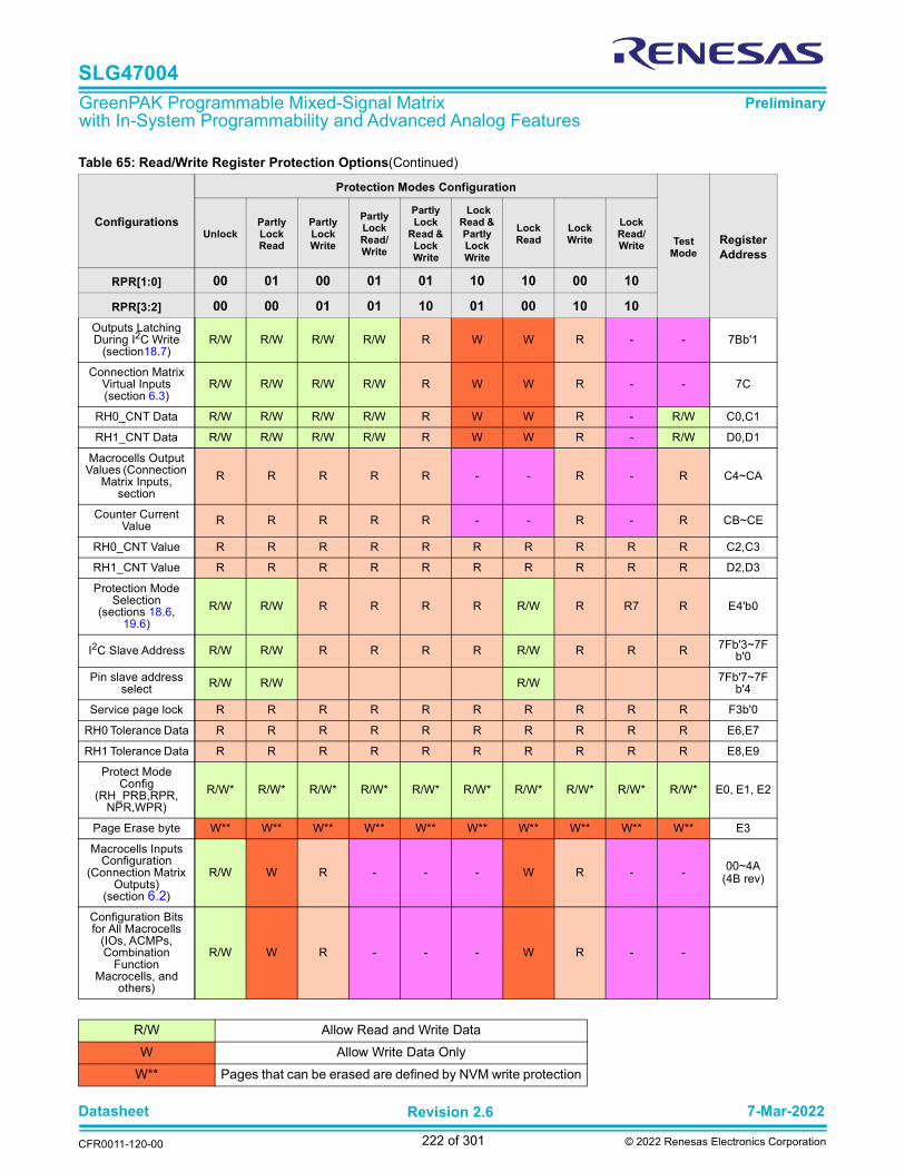
Datasheet 7-Mar-2022
CFR0011-120-00
Revision 2.6
222 of 301 © 2022 Renesas Electronics Corporation
SLG47004
GreenPAK Programmable Mixed-Signal Matrix with In-System Programmability and Advanced Analog Features
Preliminary
Outputs Latching During I2C Write
(section18.7)R/W R/W R/W R/W R W W R - - 7Bb'1
Connection Matrix Virtual Inputs(section 6.3)
R/W R/W R/W R/W R W W R - - 7C
RH0_CNT Data R/W R/W R/W R/W R W W R - R/W C0,C1
RH1_CNT Data R/W R/W R/W R/W R W W R - R/W D0,D1
Macrocells Output Values (Connection
Matrix Inputs, section
R R R R R - - R - R C4~CA
Counter Current Value R R R R R - - R - R CB~CE
RH0_CNT Value R R R R R R R R R R C2,C3
RH1_CNT Value R R R R R R R R R R D2,D3
Protection Mode Selection
(sections 18.6, 19.6)
R/W R/W R R R R R/W R R7 R E4'b0
I2C Slave Address R/W R/W R R R R R/W R R R 7Fb'3~7Fb'0
Pin slave address select R/W R/W R/W 7Fb'7~7F
b'4
Service page lock R R R R R R R R R R F3b'0
RH0 Tolerance Data R R R R R R R R R R E6,E7
RH1 Tolerance Data R R R R R R R R R R E8,E9
Protect Mode Config
(RH_PRB,RPR,NPR,WPR)
R/W* R/W* R/W* R/W* R/W* R/W* R/W* R/W* R/W* R/W* E0, E1, E2
Page Erase byte W** W** W** W** W** W** W** W** W** W** E3
Macrocells Inputs Configuration
(Connection Matrix Outputs)
(section 6.2)
R/W W R - - - W R - - 00~4A(4B rev)
Configuration Bits for All Macrocells
(IOs, ACMPs, Combination
Function Macrocells, and
others)
R/W W R - - - W R - -
R/W Allow Read and Write Data
W Allow Write Data Only
W** Pages that can be erased are defined by NVM write protection
Table 65: Read/Write Register Protection Options(Continued)
Configurations
Protection Modes Configuration
Test Mode
Register
Address
UnlockPartly Lock Read
Partly Lock Write
Partly Lock Read/Write
Partly Lock
Read & Lock Write
Lock Read & Partly Lock Write
Lock Read
Lock Write
Lock Read/Write
RPR[1:0] 00 01 00 01 01 10 10 00 10
RPR[3:2] 00 00 01 01 10 01 00 10 10

Datasheet 7-Mar-2022
CFR0011-120-00
Revision 2.6
223 of 301 © 2022 Renesas Electronics Corporation
SLG47004
GreenPAK Programmable Mixed-Signal Matrix with In-System Programmability and Advanced Analog Features
Preliminary
Note 1 R/W becomes read only if protection mode selection (lock bit) is set to 1.
Note 2 R/W Readable/writable depend on the "Trim mode enable" bit. If “Trim mode enable” bit value = 1, then trim bits areenable.
It is possible to read some data from macrocells, such as counter current value, connection matrix, and connection matrix virtualinputs. The I2C write will not have any impact on data in case data comes from macrocell output, except Connection Matrix VirtualInputs. The silicon identification service bits allow identifying silicon family, its revision, and others.
R/W* - Becomes read only after PRL is high.See Section 21 for detailed information on all registers.
R Allow Read Data Only
- The Data is protected for Read and Write

Datasheet 7-Mar-2022
CFR0011-120-00
Revision 2.6
224 of 301 © 2022 Renesas Electronics Corporation
SLG47004
GreenPAK Programmable Mixed-Signal Matrix with In-System Programmability and Advanced Analog Features
Preliminary
18.7 I2C ADDITIONAL OPTIONS
When Output latching during I2C write to the register configuration data (block address A10, A9, A8 = 000), registers [985] = 1allows all PINs output value to be latched while register content is changing. It will protect the output change due to configurationprocess during I2C write in case multiple register bytes are changed. Inputs and internal macrocells retain their status during I2Cwrite.
See Section 21 for detailed information on all registers.
18.7.1 Reading Counter Data via I2C
The current count value in three counters in the device can be read via I2C. The counters that have this additional functionalityare 16-bit CNT0, and 8-bit counters CNT2 and CNT4.
18.7.2 I2C Byte Write Bit Masking
The I2C macrocell inside SLG47004 supports masking of individual bits within a byte that is written to the RAM memory space.This function is supported across the entire RAM memory space. To implement this function, the user performs a Byte WriteCommand (see Section 18.4.1 for details) on the I2C Byte Write Mask Register (address 0F6H) with the desired bit mask pattern.This sets a bit mask pattern for the target memory location that will take effect on the next Byte Write Command to this registerbyte. Any bit in the mask that is set to “1” in the I2C Byte Write Mask Register will mask the effect of changing that particular bitin the target register, during the next Byte Write Command. The contents of the I2C Byte Write Mask Register are reset (set to00h) after valid Byte Write Command. If the next command received by the device is not a Byte Write Command, the effect of thebit masking function will be aborted, and the I2C Byte Write Mask Register will be reset with no effect. Figure 243 shows anexample of this function.

Datasheet 7-Mar-2022
CFR0011-120-00
Revision 2.6
225 of 301 © 2022 Renesas Electronics Corporation
SLG47004
GreenPAK Programmable Mixed-Signal Matrix with In-System Programmability and Advanced Analog Features
Preliminary
Figure 243: Example of I2C Byte Write Bit Masking
User Actions
Byte Write Command, Address = C9, Data = 11110000b [sets mask bits] Byte Write Command, Address = 74h, Data = 10101010b [writes data with mask]
1
Memory Address 74h (original contents)
Memory Address 74h (new data in write command)
Memory Address C9 (mask register)
Memory Address 74h (new contents after write command)
Mask to choose bit from newwrite command
Bit from original registercontents
Bit from new write command
Mask to choose bit fromoriginal register contents
1 0 0 1 1 0 0
1 0 1 0 1 0 1 0
1 1 1 1 0 0 0 0
1 1 0 0 1 0 1 0

Datasheet 7-Mar-2022
CFR0011-120-00
Revision 2.6
226 of 301 © 2022 Renesas Electronics Corporation
SLG47004
GreenPAK Programmable Mixed-Signal Matrix with In-System Programmability and Advanced Analog Features
Preliminary
19 Non-Volatile Memory
The SLG47004 provides 2,048 bits of Serial Electrically Erasable Configuration Register memory that is used for deviceconfiguration, and 2,048 bits Programmable Read-Only Memory (emulated EEPROM). Each of these memory spaces is internallyorganized as 16 pages of 16 bytes. The device features a Software Write Protection feature with five different programmablelevels of protection for the emulated EEPROM array. The protection settings of the device can be made permanent if desired.The emulated EEPROM memory operates with a supply voltage ranging from 2.4 V to 5.5 V for Read and 2.5 V to 5.5 V for Write.
The emulated EEPROM inside the SLG47004 operates as a slave device and utilizes a simple I2C compatible 2-wire digital serialinterface to communicate with a host controller commonly referred to as the bus Master. The Master initiates and controls all readand write operations to the Slave devices on the serial bus, and both the Master and the Slave devices can transmit and receivedata on the bus.
Key features:
Low-voltage Operation for Read: VCC = 2.4 V to 5.5 V for Write: VCC = 2.5 V to 5.5 V
I2C-Compatible (2-Wire) Serial Interface 100 kHz Standard Mode 400 kHz Fast Mode (FM)
Software Write Protection of the EEPROM Emulation Array Five configuration options Protection settings can be made permanent
Low Current Consumption Read Current 0.5 mA max Page Write Current 3.0 mA max Chip Erase Current 3.0 mA max Standby Current (1.0 μA max)
16-byte Page Write Mode Self-timed Write/Erase Cycle (20 ms max) Reliability
Endurance: 1,000 write cycles Data retention: 10 years at 125 °C
19.1 SERIAL NVM WRITE OPERATIONS
Write access to the NVM is possible by setting A3, A2, A1, A0 to “0000”, which allows serial write data for a single page only.Upon receipt of the proper Control Byte and Word Address bytes, the SLG47004 will send an ACK. The device will then be readyto receive page data, which is 16 sequential writes of 8-bit data words. The SLG47004 will respond with an ACK after each dataword is received. The addressing device, such as a bus Master, must then terminate the write operation with a Stop conditionafter all page data is written. At that time the device will enter an internally self-timed write cycle, which will be completed withintWR (20 ms). While the data is being written into the NVM Memory Array, all inputs, outputs, internal logic, and I2C access to theRegister data will be operational/valid. Please refer to Figure 245 for the SLG47004 Memory Map.
Note: The 16 programmed bytes should be in the same page. Any I2C command that does not meet specific requirements willbe ignored and NVM will remain unprogrammed.
Note: Special care must be taken when NVM page 14 is rewritten (registers [1919:1792]). This page contains rheostatstolerance data that can be permanently lost during write/erase operation.
SLG47004 will ignore the Serial NVM Write command in case the self-programming procedure for programming rheostat valueinto the NVM is in progress. The SLG47004 will respond with NACK in this case. Please refer to the Acknowledge Pollingsection for more details.

Datasheet 7-Mar-2022
CFR0011-120-00
Revision 2.6
227 of 301 © 2022 Renesas Electronics Corporation
SLG47004
GreenPAK Programmable Mixed-Signal Matrix with In-System Programmability and Advanced Analog Features
Preliminary
Data “1” cannot be re-programmed as data “0” without erasure. Each byte can only be programmed one time without erasure.
A10 will be ignored during communication to SLG47004.
A9 = 1 will enable access to the NVM.
A9 = 1 and A8 = 0 corresponds to the 2K bits chip configuration NVM data.
A9 = 1 and A8 = 1 corresponds to the 2K bits of emulated EEPROM data.
A3, A2, A1, and A0 should be 0000 for the page write operation.
In a single page, if the data written to any byte is 00H, the contents of the matching byte in NVM memory will not be altered.
Figure 244: Page Write Command
X X X XA10
A9
A8 W
Control Byte Word Address (n)
Control Code
Block Address
R/W bit
S ACK
AcknowledgebitStart
bit Data (n)
Stopbit
SDA LINE
Bus Activity
ACK
Data (n + 1)
ACK ACK
Data (n + 15)
P
Acknowledgebit
ACKA7
A6
A5
A4
A3
A2
A1
A0

Datasheet 7-Mar-2022
CFR0011-120-00
Revision 2.6
228 of 301 © 2022 Renesas Electronics Corporation
SLG47004
GreenPAK Programmable Mixed-Signal Matrix with In-System Programmability and Advanced Analog Features
Preliminary
19.2 SERIAL NVM READ OPERATIONS
There are three read operations:
Current Address Read Random Address Read Sequential Read
Please refer to the Section 18 for more details.
19.3 SERIAL NVM ERASE OPERATIONS
The erase scheme allows a portion or the entire emulated EEPROM including the 2K bits NVM chip configuration to be erasedby modifying the contents of the Erase Registers (ERSE <2:0>). Changing the state of the ERSE is accomplished with a ByteWrite sequence with the requirements outlined in this section.
The ERSE registers are located on byte E3h.
The ERSE format is shown in Table 66, and the ERSE bit functions are included in Table 67.
Figure 245: I2C Block Addressing
Table 66: Erase Register Bit Format
b7 b6 b5 b4 b3 b2 b1 b0
Page Erase Register ERSE2 ERSE1 ERSE0 ERSEB4 ERSEB3 ERSEB2 ERSEB1 ERSEB0
2 kbits Register Data Configuration
Not Used
2 kbits NVM Data Configuration
2 kbits EEPROM
Not Used
I2C Block Address Memory Space
A10 = 0
A10 = 0
A10 = 0
A10 = 0
A10 = 1
A9 = 0
A9 = 0
A9 = 1
A9 = 1
A9 = X
A8 = 0
A8 = 1
A8 = 0
A8 = 1
A8 = X
Lowest I2C Address = 000h
Highest I2C Address = 7FFh
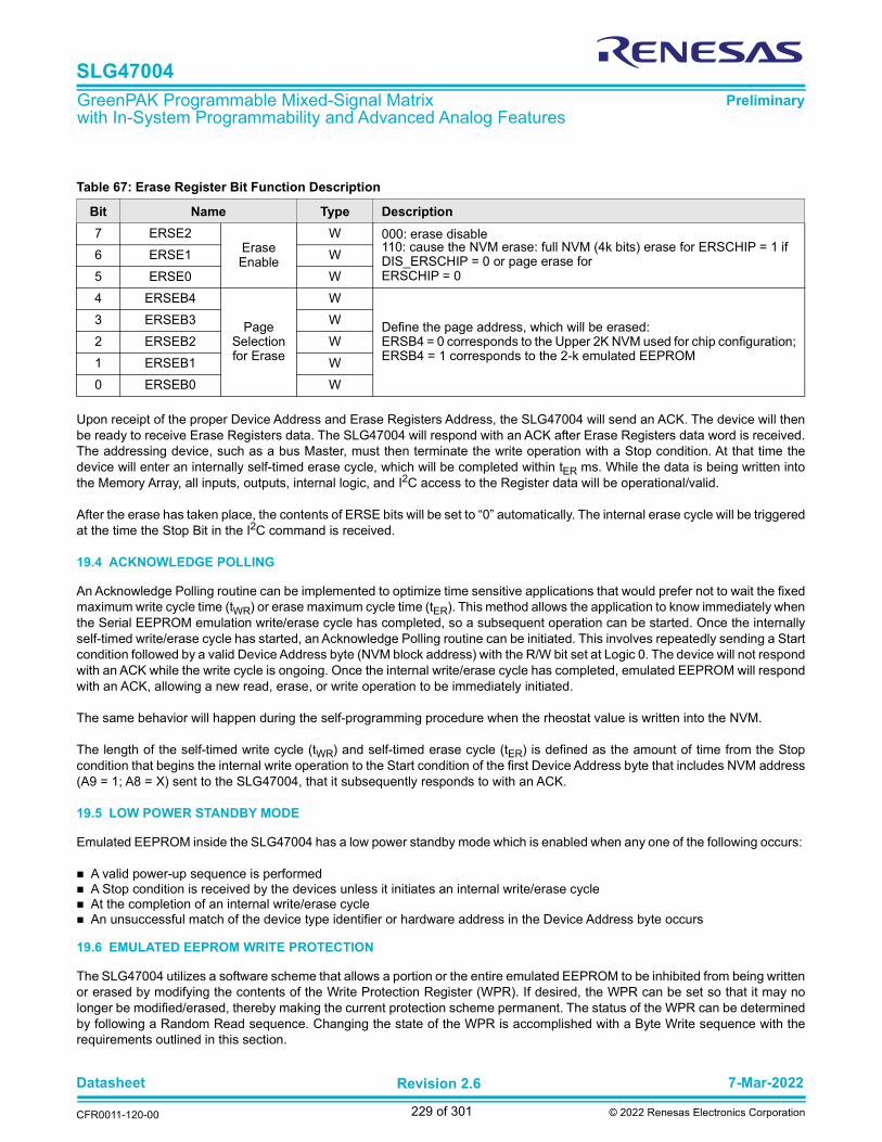
Datasheet 7-Mar-2022
CFR0011-120-00
Revision 2.6
229 of 301 © 2022 Renesas Electronics Corporation
SLG47004
GreenPAK Programmable Mixed-Signal Matrix with In-System Programmability and Advanced Analog Features
Preliminary
Upon receipt of the proper Device Address and Erase Registers Address, the SLG47004 will send an ACK. The device will thenbe ready to receive Erase Registers data. The SLG47004 will respond with an ACK after Erase Registers data word is received.The addressing device, such as a bus Master, must then terminate the write operation with a Stop condition. At that time thedevice will enter an internally self-timed erase cycle, which will be completed within tER ms. While the data is being written intothe Memory Array, all inputs, outputs, internal logic, and I2C access to the Register data will be operational/valid.
After the erase has taken place, the contents of ERSE bits will be set to “0” automatically. The internal erase cycle will be triggeredat the time the Stop Bit in the I2C command is received.
19.4 ACKNOWLEDGE POLLING
An Acknowledge Polling routine can be implemented to optimize time sensitive applications that would prefer not to wait the fixedmaximum write cycle time (tWR) or erase maximum cycle time (tER). This method allows the application to know immediately whenthe Serial EEPROM emulation write/erase cycle has completed, so a subsequent operation can be started. Once the internallyself-timed write/erase cycle has started, an Acknowledge Polling routine can be initiated. This involves repeatedly sending a Startcondition followed by a valid Device Address byte (NVM block address) with the R/W bit set at Logic 0. The device will not respondwith an ACK while the write cycle is ongoing. Once the internal write/erase cycle has completed, emulated EEPROM will respondwith an ACK, allowing a new read, erase, or write operation to be immediately initiated.
The same behavior will happen during the self-programming procedure when the rheostat value is written into the NVM.
The length of the self-timed write cycle (tWR) and self-timed erase cycle (tER) is defined as the amount of time from the Stopcondition that begins the internal write operation to the Start condition of the first Device Address byte that includes NVM address(A9 = 1; A8 = X) sent to the SLG47004, that it subsequently responds to with an ACK.
19.5 LOW POWER STANDBY MODE
Emulated EEPROM inside the SLG47004 has a low power standby mode which is enabled when any one of the following occurs:
A valid power-up sequence is performed A Stop condition is received by the devices unless it initiates an internal write/erase cycle At the completion of an internal write/erase cycle An unsuccessful match of the device type identifier or hardware address in the Device Address byte occurs
19.6 EMULATED EEPROM WRITE PROTECTION
The SLG47004 utilizes a software scheme that allows a portion or the entire emulated EEPROM to be inhibited from being writtenor erased by modifying the contents of the Write Protection Register (WPR). If desired, the WPR can be set so that it may nolonger be modified/erased, thereby making the current protection scheme permanent. The status of the WPR can be determinedby following a Random Read sequence. Changing the state of the WPR is accomplished with a Byte Write sequence with therequirements outlined in this section.
Table 67: Erase Register Bit Function Description
Bit Name Type Description
7 ERSE2Erase Enable
W 000: erase disable 110: cause the NVM erase: full NVM (4k bits) erase for ERSCHIP = 1 ifDIS_ERSCHIP = 0 or page erase for ERSCHIP = 0
6 ERSE1 W
5 ERSE0 W
4 ERSEB4
Page Selection for Erase
W
Define the page address, which will be erased:ERSB4 = 0 corresponds to the Upper 2K NVM used for chip configuration;ERSB4 = 1 corresponds to the 2-k emulated EEPROM
3 ERSEB3 W
2 ERSEB2 W
1 ERSEB1 W
0 ERSEB0 W
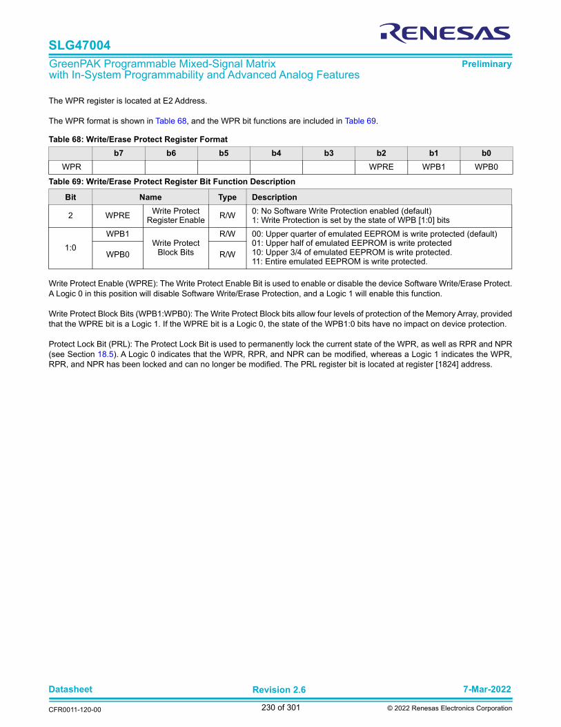
Datasheet 7-Mar-2022
CFR0011-120-00
Revision 2.6
230 of 301 © 2022 Renesas Electronics Corporation
SLG47004
GreenPAK Programmable Mixed-Signal Matrix with In-System Programmability and Advanced Analog Features
Preliminary
The WPR register is located at E2 Address.
The WPR format is shown in Table 68, and the WPR bit functions are included in Table 69.
Write Protect Enable (WPRE): The Write Protect Enable Bit is used to enable or disable the device Software Write/Erase Protect.A Logic 0 in this position will disable Software Write/Erase Protection, and a Logic 1 will enable this function.
Write Protect Block Bits (WPB1:WPB0): The Write Protect Block bits allow four levels of protection of the Memory Array, providedthat the WPRE bit is a Logic 1. If the WPRE bit is a Logic 0, the state of the WPB1:0 bits have no impact on device protection.
Protect Lock Bit (PRL): The Protect Lock Bit is used to permanently lock the current state of the WPR, as well as RPR and NPR(see Section 18.5). A Logic 0 indicates that the WPR, RPR, and NPR can be modified, whereas a Logic 1 indicates the WPR,RPR, and NPR has been locked and can no longer be modified. The PRL register bit is located at register [1824] address.
Table 68: Write/Erase Protect Register Format
b7 b6 b5 b4 b3 b2 b1 b0
WPR WPRE WPB1 WPB0
Table 69: Write/Erase Protect Register Bit Function Description
Bit Name Type Description
2 WPRE Write Protect Register Enable R/W 0: No Software Write Protection enabled (default)
1: Write Protection is set by the state of WPB [1:0] bits
1:0
WPB1Write Protect
Block Bits
R/W 00: Upper quarter of emulated EEPROM is write protected (default)01: Upper half of emulated EEPROM is write protected10: Upper 3/4 of emulated EEPROM is write protected.11: Entire emulated EEPROM is write protected.
WPB0 R/W

Datasheet 7-Mar-2022
CFR0011-120-00
Revision 2.6
231 of 301 © 2022 Renesas Electronics Corporation
SLG47004
GreenPAK Programmable Mixed-Signal Matrix with In-System Programmability and Advanced Analog Features
Preliminary
20 Analog Temperature Sensor
The SLG47004 has an Analog Temperature sensor (TS) with an output voltage linearly-proportional to the Centigradetemperature. The TS cell shares buffer with Vref 0, so it is impossible to use both cells simultaneously, its output can be connecteddirectly to the IO0 or IO1 or the ACPM1_L positive input. Using buffer causes low-output impedance, linear output and makesinterfacing to readout or control circuitry especially easy. Vref0 and Vref1 share output buffers with Temperature sensor. Note,that user can use any of output buffers, but Temperature sensor is calibrated for Vref1 output buffer. The TS is rated to operateover a -40 °C to 85 °C temperature range. The error in the whole temperature range does not exceed ±1.76 %. For more detailsrefer to Section 3.12.
where:
VTS1 (mV) - TS Output Voltage, range 1
VTS2 (mV) - TS Output Voltage, range 2
T (°C) - Temperature
VTS1 = -2.3 x T + 907.4
VTS2 = -2.8 x T + 1095.4

Datasheet 7-Mar-2022
CFR0011-120-00
Revision 2.6
232 of 301 © 2022 Renesas Electronics Corporation
SLG47004
GreenPAK Programmable Mixed-Signal Matrix with In-System Programmability and Advanced Analog Features
Preliminary
Figure 246: Analog Temperature Sensor Structure Diagram
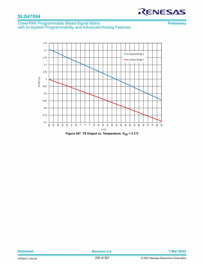
Datasheet 7-Mar-2022
CFR0011-120-00
Revision 2.6
233 of 301 © 2022 Renesas Electronics Corporation
SLG47004
GreenPAK Programmable Mixed-Signal Matrix with In-System Programmability and Advanced Analog Features
Preliminary
Figure 247: TS Output vs. Temperature, VDD = 3.3 V
0.7
0.75
0.8
0.85
0.9
0.95
1
1.05
1.1
1.15
1.2
1.25
-40
-35
-30
-25
-20
-15
-10 -5 0 5
10
15
20
25
30
35
40
45
50
55
60
65
70
75
80
85
TS
OU
T (
V)
T (°C)
Output Range 2
Output Range 1

Datasheet 7-Mar-2022
CFR0011-120-00
Revision 2.6
234 of 301 © 2022 Renesas Electronics Corporation
SLG47004
GreenPAK Programmable Mixed-Signal Matrix with In-System Programmability and Advanced Analog Features
Preliminary
21 Register Definitions
21.1 REGISTER MAP
Table 70: Register Map
Address
Signal Function Register Bit DefinitionByte
Register
Bit
Matrix Output
0
0
LUT2_0 & DFF0
OUT0:IN0 of LUT2_0 or Clock Input of DFF0
123456
OUT1:IN1 of LUT2_0 or Data Input of DFF0
7
1
89
101112
LUT2_1 & DFF1
OUT2:IN0 of LUT2_1 or Clock Input of DFF1
131415
2
161718
OUT3:IN1 of LUT2_1 or Data Input of DFF1
1920212223
3
24
LUT2_2 & DFF2
OUT4:IN0 of LUT2_2 or Clock Input of DFF2
252627282930
OUT5:IN1 of LUT2_2 or Data Input of DFF2
31
4
3233343536
LUT2_3 & PGen OUT6:IN0 of LUT2_3 or Clock Input of PGen
373839

Datasheet 7-Mar-2022
CFR0011-120-00
Revision 2.6
235 of 301 © 2022 Renesas Electronics Corporation
SLG47004
GreenPAK Programmable Mixed-Signal Matrix with In-System Programmability and Advanced Analog Features
Preliminary
5
40
LUT2_3 & PGen
OUT6:IN0 of LUT2_3 or Clock Input of PGen41
42
OUT7:IN1 of LUT2_3 or nRST of PGen
4344454647
6
48
LUT3_0 & DFF3
OUT8:IN0 of LUT3_0 or CLK Input of DFF3
495051525354
OUT9:IN1 of LUT3_0 or Data Input of DFF3
55
7
5657585960
OUT10:IN2 of LUT3_0 or nRST (nSET) of DFF3
616263
8
646566
LUT3_1 & DFF4
OUT11:IN0 of LUT3_1 or CLK Input of DFF4
6768697071
9
72
OUT12:IN1 of LUT3_1 or Data Input of DFF4
737475767778
OUT13:IN2 of LUT3_1 or nRST (nSET) of DFF4
79
A
80818283
Table 70: Register Map (Continued)
Address
Signal Function Register Bit DefinitionByte
Register
Bit

Datasheet 7-Mar-2022
CFR0011-120-00
Revision 2.6
236 of 301 © 2022 Renesas Electronics Corporation
SLG47004
GreenPAK Programmable Mixed-Signal Matrix with In-System Programmability and Advanced Analog Features
Preliminary
A
84
LUT3_2 & DFF5
OUT14:IN0 of LUT3_2 or CLK Input of DFF5
858687
B
888990
OUT15:IN1 of LUT3_2 or Data Input of DFF5
9192939495
C
96
OUT16:IN2 of LUT3_2 or nRST (nSET) of DFF5
979899
100101102
LUT3_3 & DFF6
OUT17:IN0 of LUT3_3 or CLK Input of DFF6
103
D
104105106107108
OUT18:IN1 of LUT3_3 or Data Input of DFF6
109110111
E
112113114
OUT19:IN2 of LUT3_3 or nRST (nSET) of DFF6
115116117118119
F
120
LUT3_4 & DFF7
OUT20:IN0 of LUT3_4 or CLK Input of DFF7
121122123124125126 OUT21:
IN1 of LUT3_4 or Data Input of DFF7127
Table 70: Register Map (Continued)
Address
Signal Function Register Bit DefinitionByte
Register
Bit

Datasheet 7-Mar-2022
CFR0011-120-00
Revision 2.6
237 of 301 © 2022 Renesas Electronics Corporation
SLG47004
GreenPAK Programmable Mixed-Signal Matrix with In-System Programmability and Advanced Analog Features
Preliminary
10
128
LUT3_4 & DFF7
OUT21:IN1 of LUT3_4 or Data Input of DFF7
129130131132
OUT22:IN2 of LUT3_4 or nRST (nSET) of DFF7
133134135
11
136137138
LUT3_5 & DFF8
OUT23:IN0 of LUT3_5 or CLK Input of DFF8
139140141142143
12
144
OUT24:IN1 of LUT3_5 or Data Input of DFF8
145146147148149150
OUT25:IN2 of LUT3_5 or nRST (nSET) of DFF8
151
13
152153154155156
LUT3_6 & DFF9
OUT26:IN0 of LUT3_6 or CLK Input of DFF9
157158159
14
160161162
OUT27:IN1 of LUT3_6 or Data Input of DFF9
163164165166167
15
168
OUT28:IN2 of LUT3_6 or nRST (nSET) of DFF9
169170171172173
Table 70: Register Map (Continued)
Address
Signal Function Register Bit DefinitionByte
Register
Bit

Datasheet 7-Mar-2022
CFR0011-120-00
Revision 2.6
238 of 301 © 2022 Renesas Electronics Corporation
SLG47004
GreenPAK Programmable Mixed-Signal Matrix with In-System Programmability and Advanced Analog Features
Preliminary
15174
Multi_function1
OUT29:IN0 of LUT3_7 or CLK Input of DFF11Delay1 Input (or Counter1 nRST Input)
175
16
176177178179180
OUT30:IN1 of LUT3_7 or nRST (nSET) of DFF11Delay1 Input (or Counter1 nRST Input)
181182183
17
184185186
OUT31:IN2 of LUT3_7 or Data of DFF11Delay1 Input (or Counter1 nRST Input)
187188189190191
18
192
Multi_function2
OUT32:IN0 of LUT3_8 or CLK Input of DFF12Delay2 Input (or Counter2 nRST Input)
193194195196197198
OUT33:IN1 of LUT3_8 or nRST (nSET) of DFF12Delay2 Input (or Counter2 nRST Input)
199
19
200201202203204
OUT34:IN2 of LUT3_8 or Data of DFF12Delay2 Input (or Counter2 nRST Input)
205206207
1A
208209210
Multi_function3OUT35:IN0 of LUT3_9 or CLK Input of DFF13Delay3 Input (or Counter3 nRST Input)
211212213214215
Table 70: Register Map (Continued)
Address
Signal Function Register Bit DefinitionByte
Register
Bit

Datasheet 7-Mar-2022
CFR0011-120-00
Revision 2.6
239 of 301 © 2022 Renesas Electronics Corporation
SLG47004
GreenPAK Programmable Mixed-Signal Matrix with In-System Programmability and Advanced Analog Features
Preliminary
1B
216
Multi_function3
OUT36:IN1 of LUT3_9 or nRST (nSET) of DFF13Delay3 Input (or Counter3 nRST Input)
217218219220221222
OUT37:IN2 of LUT3_9 or Data of DFF13Delay3 Input (or Counter3 nRST Input)
223
1C
224225226227228
Multi_function4
OUT38:IN0 of LUT3_10 or CLK Input of DFF14Delay4 Input (or Counter4 nRST Input)
229230231
1D
232233234
OUT39:IN1 of LUT3_10 or nRST (nSET) of DFF14Delay4 Input (or Counter4 nRST Input)
235236237238239
1E
240
OUT40:IN2 of LUT3_10 or Data of DFF14Delay4 Input (or Counter4 nRST Input)
241242243244245246
Multi_function5
OUT41:IN0 of LUT3_11 or CLK Input of DFF15Delay5 Input (or Counter5 nRST Input)
247
1F
248249250251252
OUT42:IN1 of LUT3_11 or nRST (nSET) of DFF15Delay5 Input (or Counter5 nRST Input)
253254255
20
256257258
OUT43:IN2 of LUT3_11 or Data of DFF15Delay5 Input (or Counter5 nRST Input)
259260261262263
Table 70: Register Map (Continued)
Address
Signal Function Register Bit DefinitionByte
Register
Bit

Datasheet 7-Mar-2022
CFR0011-120-00
Revision 2.6
240 of 301 © 2022 Renesas Electronics Corporation
SLG47004
GreenPAK Programmable Mixed-Signal Matrix with In-System Programmability and Advanced Analog Features
Preliminary
21
264
Multi_function6
OUT44:IN0 of LUT3_12 or CLK Input of DFF16Delay6 Input (or Counter6 nRST Input)
265266267268269270
OUT45:IN1 of LUT3_12 or nRST (nSET) of DFF16Delay6 Input (or Counter6 nRST Input)
271
22
272273274275276
OUT46:IN2 of LUT3_12 or Data of DFF16Delay6 Input (or Counter6 nRST Input)
277278279
23
280281282
LUT3_13 & Pipe Delay (RIPP CNT)
OUT47:IN0 of LUT3_13 or Input of Pipe Delay or UP signal of RIPP CNT
283284285286287
24
288
OUT48:IN1 of LUT3_13 or nRST of Pipe Delay or nSET of RIPP CNT
289290291292293294
OUT49:IN2 of LUT3_13 or Clock of PipeDelay_RIPP CNT
295
25
296297298299300
LUT4_DFF10
OUT50:IN0 of LUT4_0 or CLK Input of DFF10
301302303
26
304305306
OUT51:IN1 of LUT4_0 or Data of DFF10
307308309310311
Table 70: Register Map (Continued)
Address
Signal Function Register Bit DefinitionByte
Register
Bit
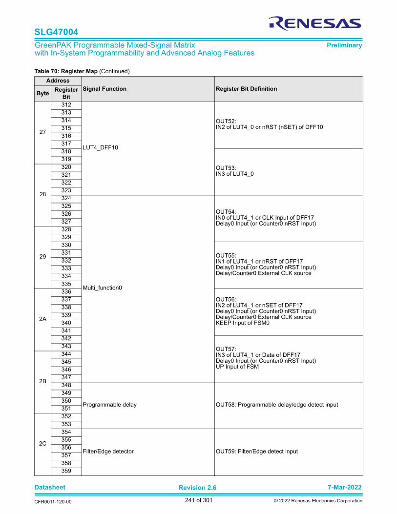
Datasheet 7-Mar-2022
CFR0011-120-00
Revision 2.6
241 of 301 © 2022 Renesas Electronics Corporation
SLG47004
GreenPAK Programmable Mixed-Signal Matrix with In-System Programmability and Advanced Analog Features
Preliminary
27
312
LUT4_DFF10
OUT52:IN2 of LUT4_0 or nRST (nSET) of DFF10
313314315316317318
OUT53:IN3 of LUT4_0
319
28
320321322323324
Multi_function0
OUT54:IN0 of LUT4_1 or CLK Input of DFF17Delay0 Input (or Counter0 nRST Input)
325326327
29
328329330
OUT55:IN1 of LUT4_1 or nRST of DFF17Delay0 Input (or Counter0 nRST Input)Delay/Counter0 External CLK source
331332333334335
2A
336OUT56:IN2 of LUT4_1 or nSET of DFF17Delay0 Input (or Counter0 nRST Input)Delay/Counter0 External CLK source KEEP Input of FSM0
337338339340341342
OUT57:IN3 of LUT4_1 or Data of DFF17Delay0 Input (or Counter0 nRST Input)UP Input of FSM
343
2B
344345346347348
Programmable delay OUT58: Programmable delay/edge detect input
349350351
2C
352353354
Filter/Edge detector OUT59: Filter/Edge detect input
355356357358359
Table 70: Register Map (Continued)
Address
Signal Function Register Bit DefinitionByte
Register
Bit

Datasheet 7-Mar-2022
CFR0011-120-00
Revision 2.6
242 of 301 © 2022 Renesas Electronics Corporation
SLG47004
GreenPAK Programmable Mixed-Signal Matrix with In-System Programmability and Advanced Analog Features
Preliminary
2D
360
IO0
OUT60: IO0 DOUT
361362363364365366
OUT61: IO0 DOUT OE
367
2E
368369370371372
IO1
OUT62: IO1 DOUT
373374375
2F
376377378
OUT63: IO1 DOUT OE
379380381382383
30
384
IO2
OUT64: IO2 DOUT
385386387388389390
OUT65: IO2 DOUT OE
391
31
392393394395396
IO3
OUT66: IO3 DOUT
397398399
32
400401402
OUT67: IO3 DOUT OE
403404405406407
Table 70: Register Map (Continued)
Address
Signal Function Register Bit DefinitionByte
Register
Bit

Datasheet 7-Mar-2022
CFR0011-120-00
Revision 2.6
243 of 301 © 2022 Renesas Electronics Corporation
SLG47004
GreenPAK Programmable Mixed-Signal Matrix with In-System Programmability and Advanced Analog Features
Preliminary
33
408
IO4
OUT68: IO4 DOUT
409410411412413414
OUT69: IO4 DOUT OE
415
34
416417418419420
IO5
OUT70: IO5 DOUT
421422423
35
424425426
OUT71: IO5 DOUT OE
427428429430431
36
432
IO6
OUT72: IO6 DOUT
433434435436437438
OUT73: IO6 DOUT OE
439
37
440441442443444
Programmable Trim Block0
OUT74:set0 of Auto Calibration
445446447
38
448449450
OUT75:clock0 of Auto Calibration
451452453454455
Table 70: Register Map (Continued)
Address
Signal Function Register Bit DefinitionByte
Register
Bit
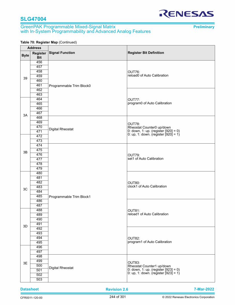
Datasheet 7-Mar-2022
CFR0011-120-00
Revision 2.6
244 of 301 © 2022 Renesas Electronics Corporation
SLG47004
GreenPAK Programmable Mixed-Signal Matrix with In-System Programmability and Advanced Analog Features
Preliminary
39
456
Programmable Trim Block0
OUT76:reload0 of Auto Calibration
457458459460461462
OUT77:program0 of Auto Calibration
463
3A
464465466467468
Digital Rheostat
OUT78:Rheostat Counter0 up/down0: down, 1: up. (register [920] = 0)0: up, 1: down. (register [920] = 1)
469470471
3B
472473474
Programmable Trim Block1
OUT79:set1 of Auto Calibration
475476477478479
3C
480
OUT80: clock1 of Auto Calibration
481482483484485486
OUT81:reload1 of Auto Calibration
487
3D
488489490491492
OUT82: program1 of Auto Calibration
493494495
3E
496497498
Digital Rheostat
OUT83:Rheostat Counter1 up/down0: down, 1: up. (register [923] = 0)0: up, 1: down. (register [923] = 1)
499500501502503
Table 70: Register Map (Continued)
Address
Signal Function Register Bit DefinitionByte
Register
Bit

Datasheet 7-Mar-2022
CFR0011-120-00
Revision 2.6
245 of 301 © 2022 Renesas Electronics Corporation
SLG47004
GreenPAK Programmable Mixed-Signal Matrix with In-System Programmability and Advanced Analog Features
Preliminary
3F
504
FIFO Reset of PT blocksOUT84:FIFO nRST of the control logic of reload0/reload1/auto program0/auto program1
505506507508509510
Chopper ACMP OUT85:Chopper ACMP Power Up
511
40
512513514515516
Digital Rheostat OUT86:Rheostat Charge pump enable
517518519
41
520521522
Analog Switch0 OUT87:ASW0 enable/Half bridge enable
523524525526527
42
528
Analog Switch1 OUT88:ASW1 enable/Half bridge data
529530531532533534
ACMP0 OUT89:ACMP0 Power Up
535
43
536537538539540
ACMP1 OUT90:ACMP1 Power Up
541542543
44
544545546
OSC0 OUT91:OSC0 ENABLE
547548549550551
Table 70: Register Map (Continued)
Address
Signal Function Register Bit DefinitionByte
Register
Bit
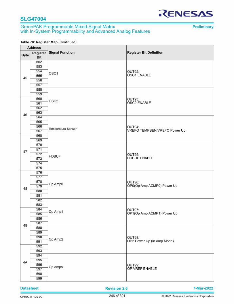
Datasheet 7-Mar-2022
CFR0011-120-00
Revision 2.6
246 of 301 © 2022 Renesas Electronics Corporation
SLG47004
GreenPAK Programmable Mixed-Signal Matrix with In-System Programmability and Advanced Analog Features
Preliminary
45
552
OSC1 OUT92:OSC1 ENABLE
553554555556557558
OSC2 OUT93:OSC2 ENABLE
559
46
560561562563564
Temperature Sensor OUT94:VREFO TEMPSEN/VREFO Power Up
565566567
47
568569570
HDBUF OUT95:HDBUF ENABLE
571572573574575
48
576
Op Amp0 OUT96:OP0(Op Amp ACMP0) Power Up
577578579580581582
Op Amp1 OUT97:OP1(Op Amp ACMP1) Power Up
583
49
584585586587588
Op Amp2 OUT98:OP2 Power Up (In Amp Mode)
589590591
4A
592593594
Op amps OUT99:OP VREF ENABLE
595596597598599
Table 70: Register Map (Continued)
Address
Signal Function Register Bit DefinitionByte
Register
Bit

Datasheet 7-Mar-2022
CFR0011-120-00
Revision 2.6
247 of 301 © 2022 Renesas Electronics Corporation
SLG47004
GreenPAK Programmable Mixed-Signal Matrix with In-System Programmability and Advanced Analog Features
Preliminary
4B
600 Reserved601 Reserved602 Reserved603 Reserved604 Reserved605 Reserved606 Reserved607 Reserved
ACMP0
4C
608 ACMP Low Energy Power Up enable(ACMP power after bg_ok) 1: enable
609 ACMP input path LPF enable 1: enable610 ACMP sampling mode enable 1: enable
611 ACMP short time wake sleep mode disable 0: short time wake sleep enable 1: short time wake sleep disable
612 ACMP wake sleep function enable 1: enable
613 ACMP Vref path LPF enable(when ACMP hysteresis > 196 mV) 1: enable
614
ACMP input divider selection
00: 1 01: 0.5 10: 1/311: 1/4
615
4D
616ACMP input mux selection
00: OP0 output01: from Pin 10: tie VDD617
618
ACMP Low to High Vref selection 000000-111111: 32 mV ~2.048 V/step = 32 mV
619620621622623
4E
624
ACMP High to Low Vref selection 000000-111111: 32 mV ~2.048 V/step = 32 mV
625626627628629
ACMP1
4E630 ACMP Low Energy Power Up enable
(ACMP power after bg_ok) 1: enable
631 ACMP input path LPF enable 1: enable
4F
632 ACMP sampling mode enable 1: enable
633 ACMP short time wake sleep mode disable 0: short time wake sleep enable 1: short time wake sleep disable
634 ACMP wake sleep function enable 1: enable
635 ACMP Vref path LPF enable(when ACMP hysteresis > 196 mV) 1: enable
636
ACMP input divider selection
00: 101: 0.510: 1/311: 1/4
637
Table 70: Register Map (Continued)
Address
Signal Function Register Bit DefinitionByte
Register
Bit

Datasheet 7-Mar-2022
CFR0011-120-00
Revision 2.6
248 of 301 © 2022 Renesas Electronics Corporation
SLG47004
GreenPAK Programmable Mixed-Signal Matrix with In-System Programmability and Advanced Analog Features
Preliminary
4F
638
ACMP input mux selection
00: OP1 output01: from Pin10: ACMP0 input mux output11: VrefO1 Temp sensor output
639
50
640
ACMP Low to High Vref selection 000000-111111:32 mV ~2.048 V/step = 32 mV
641642643644645646
ACMP High to Low Vref selection 000000-111111:32 mV ~2.048 V/step = 32 mV
647
51
648649650651
Vref
51
652 Reserved653 Reserved654 Reserved655 Reserved
52
656 Reserved657 Reserved
658 VREFO0 input source selection 0: ACMP0 VREF 1: Temp Sensor
659 VREFO0 output buffer enable 1: enable660 VREFO0 register Power Up VREFO0 register power on signal
661 VREFO0 Power Up selection 0: Power Up from reg1: from matrix
662 Reserved no use
663 VREFO1's temp sensor to ACMP1 input path en-able
Temp Sensor output to ACMP1 enable1: enable
53
664 VREFO1's temp sensor range selection 0:1V; 1:1.2V
665 VREFO1 input source selection 0: ACMP1 Vref 1: TS
666 VREFO1 output buffer enable 1: enable667 VREFO1 register Power Up VrefO1 register power on signal
668 VREFO1 Power Up selection 0: Power Up from reg1: from matrix
669 ACMP Vrefs source selection ACMP Vref gen source selection(0: VBG, 1: VDD)
670 ACMP0 external Vref enable 1:enable671 ACMP1 external Vref enable 1:enable
54 672 Reserved
54673 Reserved674 Reserved
Table 70: Register Map (Continued)
Address
Signal Function Register Bit DefinitionByte
Register
Bit

Datasheet 7-Mar-2022
CFR0011-120-00
Revision 2.6
249 of 301 © 2022 Renesas Electronics Corporation
SLG47004
GreenPAK Programmable Mixed-Signal Matrix with In-System Programmability and Advanced Analog Features
Preliminary
54
675Reserved676
677678 Reserved679 Reserved
55
680 Reserved681 Reserved682 Reserved683 Reserved684 Reserved685 Reserved686 Reserved687 Reserved
OSC1
56
688 OSC1 turn on by registerwhen matrix output enable/pd control signal = 0:0: auto on by delay cells 1: always on
689 OSC1 matrix power down or on select 0: matrix down 1: matrix on
690 OSC1 external clock source enable 0: internal OSC1 1: external clock from Pin15
691
OSC1 post divider ratio control
00: div 101: div 210: div 411: div8
692
693
OSC1 matrix divider ratio control
000: /1 001:/2010:/4011: /3100: /8101: /12110: /24 111: /64
694
695
57
696 OSC1 matrix out enable 0: disable1: enable
697 Reserved698 Reserved699 Reserved
700 OSC1 2nd output to matrix enable 0: disable1: enable
701
OSC1 2nd matrix divider ratio control
000: /1001: /2010: /4011: /3100: /8 101: /12110: /24111: /64
702
703
OSC2
Table 70: Register Map (Continued)
Address
Signal Function Register Bit DefinitionByte
Register
Bit
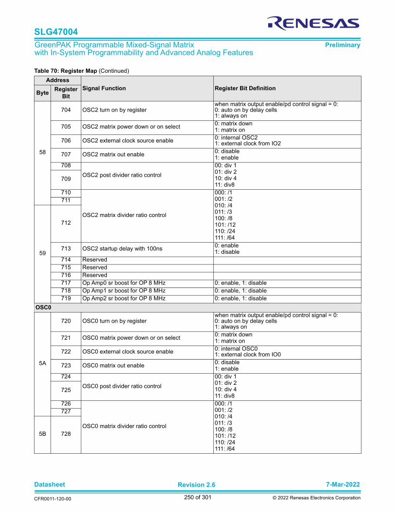
Datasheet 7-Mar-2022
CFR0011-120-00
Revision 2.6
250 of 301 © 2022 Renesas Electronics Corporation
SLG47004
GreenPAK Programmable Mixed-Signal Matrix with In-System Programmability and Advanced Analog Features
Preliminary
58
704 OSC2 turn on by registerwhen matrix output enable/pd control signal = 0:0: auto on by delay cells 1: always on
705 OSC2 matrix power down or on select 0: matrix down 1: matrix on
706 OSC2 external clock source enable 0: internal OSC21: external clock from IO2
707 OSC2 matrix out enable 0: disable1: enable
708
OSC2 post divider ratio control
00: div 101: div 2 10: div 4 11: div8
709
710
OSC2 matrix divider ratio control
000: /1001: /2 010: /4011: /3 100: /8 101: /12 110: /24 111: /64
711
59
712
713 OSC2 startup delay with 100ns 0: enable1: disable
714 Reserved715 Reserved716 Reserved717 Op Amp0 sr boost for OP 8 MHz 0: enable, 1: disable718 Op Amp1 sr boost for OP 8 MHz 0: enable, 1: disable719 Op Amp2 sr boost for OP 8 MHz 0: enable, 1: disable
OSC0
5A
720 OSC0 turn on by registerwhen matrix output enable/pd control signal = 0:0: auto on by delay cells 1: always on
721 OSC0 matrix power down or on select 0: matrix down1: matrix on
722 OSC0 external clock source enable 0: internal OSC0 1: external clock from IO0
723 OSC0 matrix out enable 0: disable 1: enable
724
OSC0 post divider ratio control
00: div 101: div 210: div 411: div8
725
726
OSC0 matrix divider ratio control
000: /1001: /2010: /4011: /3100: /8101: /12110: /24111: /64
727
5B 728
Table 70: Register Map (Continued)
Address
Signal Function Register Bit DefinitionByte
Register
Bit
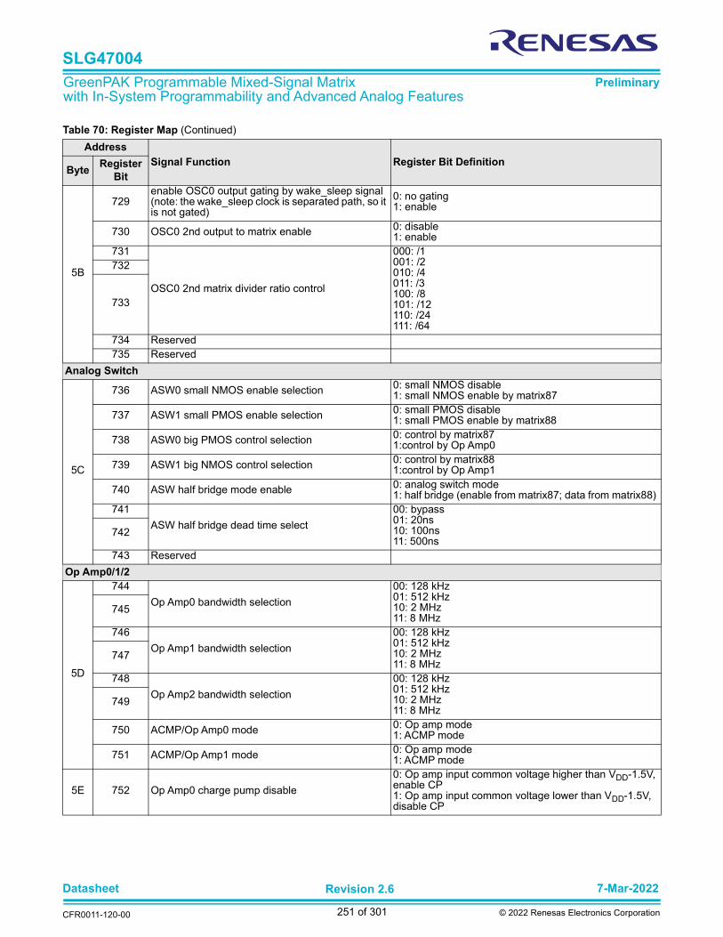
Datasheet 7-Mar-2022
CFR0011-120-00
Revision 2.6
251 of 301 © 2022 Renesas Electronics Corporation
SLG47004
GreenPAK Programmable Mixed-Signal Matrix with In-System Programmability and Advanced Analog Features
Preliminary
5B
729enable OSC0 output gating by wake_sleep signal (note: the wake_sleep clock is separated path, so it is not gated)
0: no gating1: enable
730 OSC0 2nd output to matrix enable 0: disable1: enable
731
OSC0 2nd matrix divider ratio control
000: /1001: /2 010: /4 011: /3 100: /8 101: /12110: /24111: /64
732
733
734 Reserved735 Reserved
Analog Switch
5C
736 ASW0 small NMOS enable selection 0: small NMOS disable1: small NMOS enable by matrix87
737 ASW1 small PMOS enable selection 0: small PMOS disable1: small PMOS enable by matrix88
738 ASW0 big PMOS control selection 0: control by matrix871:control by Op Amp0
739 ASW1 big NMOS control selection 0: control by matrix881:control by Op Amp1
740 ASW half bridge mode enable 0: analog switch mode1: half bridge (enable from matrix87; data from matrix88)
741
ASW half bridge dead time select
00: bypass01: 20ns10: 100ns11: 500ns
742
743 Reserved
Op Amp0/1/2
5D
744
Op Amp0 bandwidth selection
00: 128 kHz01: 512 kHz10: 2 MHz11: 8 MHz
745
746
Op Amp1 bandwidth selection
00: 128 kHz01: 512 kHz10: 2 MHz11: 8 MHz
747
748
Op Amp2 bandwidth selection
00: 128 kHz01: 512 kHz10: 2 MHz11: 8 MHz
749
750 ACMP/Op Amp0 mode 0: Op amp mode1: ACMP mode
751 ACMP/Op Amp1 mode 0: Op amp mode1: ACMP mode
5E 752 Op Amp0 charge pump disable
0: Op amp input common voltage higher than VDD-1.5V, enable CP1: Op amp input common voltage lower than VDD-1.5V, disable CP
Table 70: Register Map (Continued)
Address
Signal Function Register Bit DefinitionByte
Register
Bit

Datasheet 7-Mar-2022
CFR0011-120-00
Revision 2.6
252 of 301 © 2022 Renesas Electronics Corporation
SLG47004
GreenPAK Programmable Mixed-Signal Matrix with In-System Programmability and Advanced Analog Features
Preliminary
5E
753 Op Amp1 charge pump disable
0: Op amp input common voltage higher than VDD-1.5V, enable CP;1: Op amp input common voltage lower than VDD-1.5V, disable CP
754 Op Amp2 charge pump disable
0: Op amp input common voltage higher than VDD-1.5V, enable CP1: Op amp input common voltage lower than VDD-1.5V, disable CP
755 Path between Op Amp0/1 and Op Amp2 0: path on (for normal function)1: path off (for trim function)
756 Op Amp2's Vref buffer bypass control 0: without buffer1: with buffer
757 Supporting blocks for Op Amp0 on/off0: on/off follows op amp1: always on except input common voltage of op amp low-er than VDD-1.5 V
758 Supporting blocks for Op Amp1 on/off0: on/off follows op amp1: always on except input common voltage of op amp low-er than VDD-1.5V
759 Supporting blocks for Op Amp2 on/off0: on/off follows op amp1: always on except input common voltage of op amp low-er than VDD-1.5V
5F
760 Op amp ACMP Vref0 output selection[0]
000000-111111: 32 mV ~2.048 V/step = 32 mV
761 Op amp ACMP Vref0 output selection[1]762 Op amp ACMP Vref0 output selection[2]763 Op amp ACMP Vref0 output selection[3]764 Op amp ACMP Vref0 output selection[4]765 Op amp ACMP Vref0 output selection[5]
766 Op amp ACMP Vref0 register enable(select by register [782])
0: dynamic on/off1: Vref enable
767 Vref0 to op amp/ACMP input enable 0:disable; 1: enable
60
768 Op amp ACMP Vref1 output selection[0]
000000-111111: 32 mV ~2.048 V/step = 32 mV
769 Op amp ACMP Vref1 output selection[1]770 Op amp ACMP Vref1 output selection[2]771 Op amp ACMP Vref1 output selection[3]772 Op amp ACMP Vref1 output selection[4]773 Op amp ACMP Vref1 output selection[5]
774 Op amp ACMP Vref1 register enable(select by register [783])
0: dynamic on/off 1: Vref enable
775 Vref1 to op amp/ACMP input enable 0:disable; 1: enable
61
776 Op amp ACMP Vref0 output selection 0: Vref to ACMP negative input 1: Vref to ACMP positive input
777 Op amp ACMP Vref1 output selection 0: Vref to ACMP negative input 1: Vref to ACMP positive input
778 Reserved 779 Reserved
780 Op amp ACMP Vref0 input voltage selection 0: 2.048 V1: VDD
781 Op amp ACMP Vref1 input voltage selection 0: 2.048 V1: VDD
782 Op amp ACMP vref0 enable selection 0: from register [766]1: from matrix99
61 783 Op amp ACMP vref1 enable selection 0: from register [774]1: from matrix99
Table 70: Register Map (Continued)
Address
Signal Function Register Bit DefinitionByte
Register
Bit

Datasheet 7-Mar-2022
CFR0011-120-00
Revision 2.6
253 of 301 © 2022 Renesas Electronics Corporation
SLG47004
GreenPAK Programmable Mixed-Signal Matrix with In-System Programmability and Advanced Analog Features
Preliminary
LUT3_2/DFF5
62
784
LUT3_2_DFF5 setting
<2:0>: LUT3_2 <2:0>785786
787
<3>:LUT3_2 <3>/DFF5 Active level selection for RST/SET 0: Active low level reset/set,1: Active high level reset/set
788<4>:LUT3_2<4>/DFF50: RSTB from Matrix Output, 1: SETB from Matrix Output
789 <5>:LUT3_2 <5>/DFF5 Initial Polarity Select 0: Low, 1: High
790 <6>:LUT3_2 <6>/DFF5 Output Select0: Q output, 1: QB output
791 <7>:LUT3_2 <7>/DFF5 or Latch Select0: DFF function, 1: Latch function
LUT3_3/DFF6
63
792
LUT3_3_DFF6 setting
<2:0>: LUT3_3 <2:0>793794
795<3>:LUT3_3 <3>/DFF6 Active level selection for RST/SET 0: Active low level reset/set, 1: Active high level reset/set
796<4>:LUT3_3<4>/DFF6 0: RSTB from Matrix Output, 1: SETB from Matrix Output
797 <5>:LUT3_3 <5>/DFF6 Initial Polarity Select 0: Low, 1: High
798 <6>:LUT3_3 <6>/DFF6 Output Select 0: Q output, 1: QB output
799 <7>:LUT3_3 <7>/DFF6 or Latch Select 0: DFF function, 1: Latch function
LUT3_4/DFF7
64
800
LUT3_4_DFF7 setting
<2:0>: LUT3_4 <2:0>801802
803<3>:LUT3_4 <3>/DFF7 Active level selection for RST/SET 0: Active low level reset/set, 1: Active high level reset/set
804 <4>:LUT3_4<4>/DFF70: RSTB from Matrix Output, 1: SETB from Matrix Output
805 <5>:LUT3_4 <5>/DFF7 Initial Polarity Select0: Low, 1: High
806 <6>:LUT3_4 <6>/DFF7 Output Select0: Q output, 1: QB output
64 807 LUT3_4_DFF7 setting <7>:LUT3_4 <7>/DFF7 or Latch Select0: DFF function, 1: Latch function
LUT3_5/DFF8
Table 70: Register Map (Continued)
Address
Signal Function Register Bit DefinitionByte
Register
Bit

Datasheet 7-Mar-2022
CFR0011-120-00
Revision 2.6
254 of 301 © 2022 Renesas Electronics Corporation
SLG47004
GreenPAK Programmable Mixed-Signal Matrix with In-System Programmability and Advanced Analog Features
Preliminary
65
808
LUT3_5_DFF8 setting
<2:0>: LUT3_5 <2:0>809810
811<3>:LUT3_5 <3>/DFF8 Active level selection for RST/SET 0: Active low level reset/set, 1: Active high level reset/set
812 <4>:LUT3_5<4>/DFF80: RSTB from Matrix Output, 1: SETB from Matrix Output
813 <5>:LUT3_5 <5>/DFF8 Initial Polarity Select 0: Low, 1: High
814 <6>:LUT3_5 <6>/DFF8 Output Select0: Q output, 1: QB output
815 <7>:LUT3_5 <7>/DFF8 or Latch Select0: DFF function, 1: Latch function
LUT3_6/DFF9
66
816
LUT3_6_DFF9 setting
<2:0>: LUT3_6 <2:0>817818
819<3>:LUT3_6 <3>/DFF9 Active level selection for RST/SET 0: Active low level reset/set, 1: Active high level reset/set
820<4>:LUT3_6<4>/DFF9 0: RSTB from Matrix Output, 1: SETB from Matrix Output
821 <5>:LUT3_6 <5>/DFF9 Initial Polarity Select 0: Low, 1: High
822 <6>:LUT3_6 <6>/DFF9 Output Select 0: Q output, 1: QB output
823 <7>:LUT3_6 <7>/DFF9 or Latch Select 0: DFF function, 1: Latch function
67
824 LUT3_2 or DFF5 Select 0: LUT3_21: DFF5
825 LUT3_3 or DFF6 Select 0: LUT3_31: DFF6
826 LUT3_4 or DFF7 Select 0: LUT3_41: DFF7
827 LUT3_5 or DFF8 Select 0: LUT3_51: DFF8
828 LUT3_6 or DFF9 Select 0: LUT3_51: DFF8
829 LUT4_0 or DFF10 Select 0: LUT4_01: DFF10
830 Reserved831 Reserved
LUT4_0/DFF10
Table 70: Register Map (Continued)
Address
Signal Function Register Bit DefinitionByte
Register
Bit

Datasheet 7-Mar-2022
CFR0011-120-00
Revision 2.6
255 of 301 © 2022 Renesas Electronics Corporation
SLG47004
GreenPAK Programmable Mixed-Signal Matrix with In-System Programmability and Advanced Analog Features
Preliminary
68
832
LUT4_0_DFF10 setting
<9:0>: LUT4_0 <9:0>
833834835836837838839
69
840841
842 <10>:LUT4_0 <10>/DFF10 stage selection0: Q of first DFF; 1 Q of second DFF
843<11>:LUT4_0 <11>/DFF10 Active level selection for RST/SET 0: Active low level reset/set, 1: Active high level reset/set
844 <12>:LUT4_0 <12>/DFF10 0: RSTB from Matrix Output, 1: SETB from Matrix Output
845 <13>:LUT4_0 <13> /DFF10 Initial Polarity Select0: Low, 1: High
846 <14>:LUT4_0 <14>/DFF10 Output Select0: Q output, 1: QB output
847 <15>:LUT4_0 <15>/DFF10 or Latch Select0: DFF function, 1: Latch function
LUT3_13/Pipe Delay (RIPP CNT)
6A
848
LUT value or pipe delay out sel or nSET/END value
at LUT/pipe delay modebit<7:4>: LUT3_13 <7:4> / REG_S1<3:0> pipe delay out1 selbit<3:0>: LUT3_13 <3:0> / REG_S0<3:0> pipe delay out0 selat RIPP CNT modebit<2:0> is the nSET value. bit<5:3> is the END valuebit<6> is the range control:0: full cycle, 1: range cyclebit<7> No used
849850851852853854
855
6B
856 Active level selection for RST/SET 0: Active low level reset/set 1: Active high level reset/set
857 Out of LUT3_13 or Out0 of Pipe Delay/RIPP CNT Select
0: LUT3_131: OUT0 of Pipe Delay or RIPP CNT
858 PIPE_RIPP_CNT_S 0: Pipe delay mode selection 1: Ripple Counter mode selection
859 Pipe Delay OUT1 Polarity Select 0: Non-inverted1: Inverted
860 Reserved861 Reserved862 Reserved863 Reserved
Programmable Delay
Table 70: Register Map (Continued)
Address
Signal Function Register Bit DefinitionByte
Register
Bit
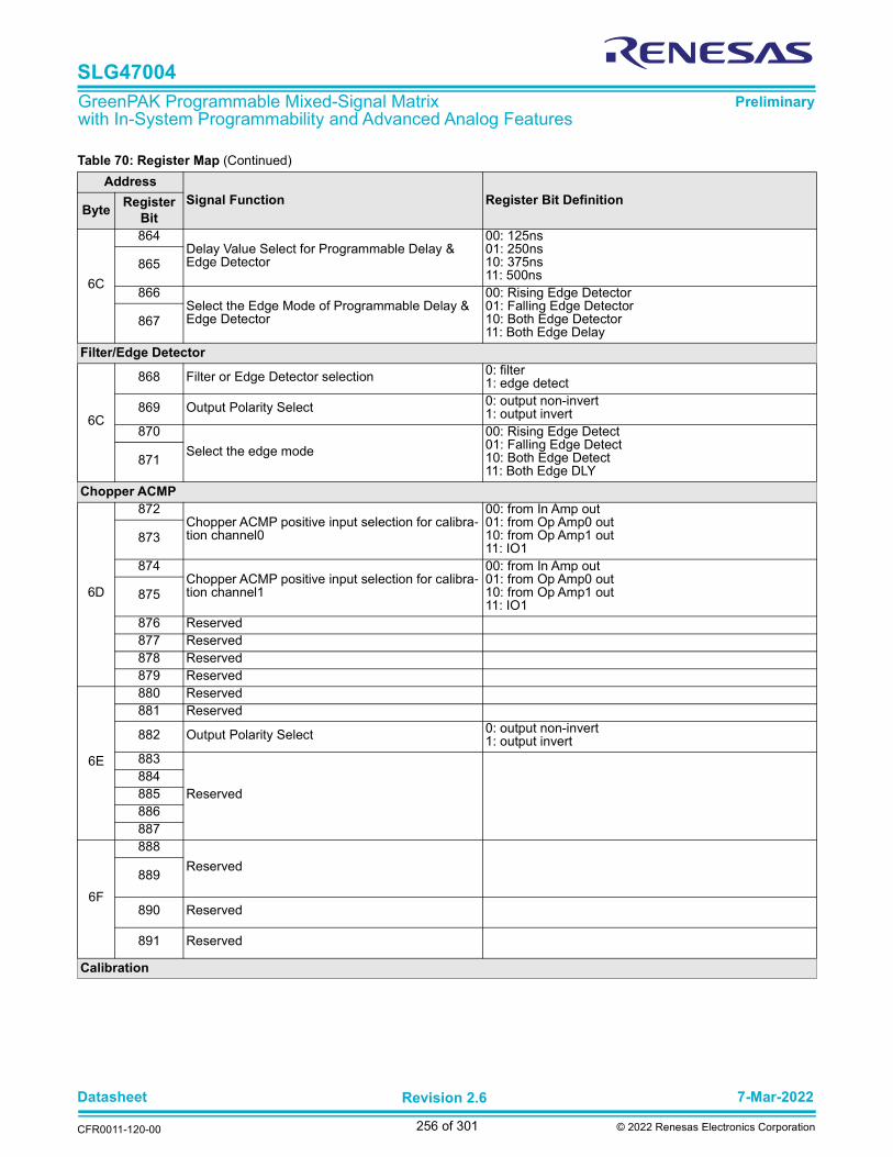
Datasheet 7-Mar-2022
CFR0011-120-00
Revision 2.6
256 of 301 © 2022 Renesas Electronics Corporation
SLG47004
GreenPAK Programmable Mixed-Signal Matrix with In-System Programmability and Advanced Analog Features
Preliminary
6C
864Delay Value Select for Programmable Delay & Edge Detector
00: 125ns01: 250ns10: 375ns11: 500ns
865
866Select the Edge Mode of Programmable Delay & Edge Detector
00: Rising Edge Detector01: Falling Edge Detector 10: Both Edge Detector11: Both Edge Delay
867
Filter/Edge Detector
6C
868 Filter or Edge Detector selection 0: filter1: edge detect
869 Output Polarity Select 0: output non-invert1: output invert
870
Select the edge mode
00: Rising Edge Detect 01: Falling Edge Detect 10: Both Edge Detect11: Both Edge DLY
871
Chopper ACMP
6D
872Chopper ACMP positive input selection for calibra-tion channel0
00: from In Amp out 01: from Op Amp0 out10: from Op Amp1 out11: IO1
873
874Chopper ACMP positive input selection for calibra-tion channel1
00: from In Amp out 01: from Op Amp0 out10: from Op Amp1 out11: IO1
875
876 Reserved877 Reserved878 Reserved879 Reserved
6E
880 Reserved881 Reserved
882 Output Polarity Select 0: output non-invert1: output invert
883
Reserved884885886887
6F
888
Reserved 889
890 Reserved
891 Reserved
Calibration
Table 70: Register Map (Continued)
Address
Signal Function Register Bit DefinitionByte
Register
Bit

Datasheet 7-Mar-2022
CFR0011-120-00
Revision 2.6
257 of 301 © 2022 Renesas Electronics Corporation
SLG47004
GreenPAK Programmable Mixed-Signal Matrix with In-System Programmability and Advanced Analog Features
Preliminary
6F
892 auto calibration channel selection by register 0: calibration channel01: calibration channel1
893 auto calibration channel selection source selection 0:calibration channel auto selection1: from register [892]
894 RH_CNT1 clock source selection0: From Chopper ACMP(Chopper ACMP changes one time per rheostat clock)1: from matrix directly
895 RH_CNT0 clock source selection0: From Chopper ACMP(Chopper ACMP changes one time per rheostat clock)1: from matrix directly
70
896
Calibration0 clock divider
0000: Reserved0001: Reserved0010: OSC1/640011: OSC1/5120100: OSC00101:OSC0/80110: OSC0/640111: OSC0/5121000: OSC0/40961001: OSC0/327681010: OSC0/262144 1011/1100/1101/1110: GND1111: EXTCLK
897898
899
900 Up/down selection 0: chopper ACMP1: matrix83
901 auto_calibration disable 0: auto calibration enable1: disable
902 Reserved 903 Reserved
71
904
Calibration1 clock divider
0000: Reserved0001: Reserved0010: OSC1/640011: OSC1/5120100: OSC00101: OSC0/80110: OSC0/640111: OSC0/5121000: OSC0/40961001: OSC0/327681010: OSC0/262144 1011/1100/1101/1110: GND1111: EXTCLK
905906
907
908 Up/down selection 0: chopper ACMP 1: matrix83
909 auto_calibration disable 0: auto calibration enable1: disable
910 Reserved 911 Reserved
Digital Rheostats
Table 70: Register Map (Continued)
Address
Signal Function Register Bit DefinitionByte
Register
Bit

Datasheet 7-Mar-2022
CFR0011-120-00
Revision 2.6
258 of 301 © 2022 Renesas Electronics Corporation
SLG47004
GreenPAK Programmable Mixed-Signal Matrix with In-System Programmability and Advanced Analog Features
Preliminary
72
912 POTCP0 turn on by register 0: control by matrix861: on
913 POTCP1 turn on by register 0: control by matrix861: on
914 POTCP0/1 clock source selection 0: from LPBG chopper OSC1: from OSC1
915 POTCP0/1 clock source select from register 0: by register [914]1: calibration auto on
916 Reserved
917 Reserved918 Reserved919 Reserved
73
920 Polarity selection of RH_CNT0 UP signal 0: default (up = 0 down mode, up = 1 up mode)1: (up = 0 up mode, up = 1 down mode)
921 Reserved 922 Reserved
923 Polarity selection of RH_CNT1 UP signal 0: default (up = 0 down mode, up = 1 up mode)1: (up = 0 up mode, up = 1 down mode)
924 Reserved 925 Reserved 926 Reserved927 Reserved
HD Buffer
74
928
Chop ACMP Vref selection for calibration channel 0
000000-111111: 1/64 ~ 64/64(divider input select by register [946])
929930931932933
934 Chop ACMP calibration channel0 external Vref se-lection
0: external Vref (pin18)1: internal Vref
935 Reserved
75
936
Chop ACMP Vref selection for calibration channel 1 000000-111111: 1/64 ~ 64/64(divider input select by register [946])
937938939940941
942 Chop ACMP calibration channel1 external Vref se-lection
0: external Vref (pin18)1: internal Vref
943 Reserved
Table 70: Register Map (Continued)
Address
Signal Function Register Bit DefinitionByte
Register
Bit

Datasheet 7-Mar-2022
CFR0011-120-00
Revision 2.6
259 of 301 © 2022 Renesas Electronics Corporation
SLG47004
GreenPAK Programmable Mixed-Signal Matrix with In-System Programmability and Advanced Analog Features
Preliminary
76
944 HD buffer register enable(select by register [945])
0: disable1: enable
945 HD buffer enable selection 0: from register [944]1: from matrix95
946 Chop ACMP Vref divider input selection0: from HD buffer output1: from op amp Vref voltage (2.048/VDD selection register in Vref block)
947 Reserved948 Reserved949 Reserved950 Reserved951 Reserved
CP OSC/Regulator
77
952 CPOSC single or multiple mode select 0: multiple OSC mode 1: single OSC mode
953 Reserved
954
CPOSC0 frequency select
00: 250 kHz01: 1 MHz10: 4 MHz11: 8 MHz
955
956 Reserved
957Reserved
958959 Reserved
78
960 Reserved961 Reserved962
CPOSC1 frequency select
00: 250 kHz01: 1 MHz10: 4 MHz11: 8 MHz
963
964 Reserved
965Reserved
966967 Reserved
79
968 Reserved
969 Reserved
970
CPOSC2 frequency select
00: 250 kHz01: 1 MHz10: 4 MHz 11: 8 MHz
971
972 Reserved973
Reserved974975 Reserved
Table 70: Register Map (Continued)
Address
Signal Function Register Bit DefinitionByte
Register
Bit

Datasheet 7-Mar-2022
CFR0011-120-00
Revision 2.6
260 of 301 © 2022 Renesas Electronics Corporation
SLG47004
GreenPAK Programmable Mixed-Signal Matrix with In-System Programmability and Advanced Analog Features
Preliminary
7A
976
Buffer Vref select
00: none01: internal Vref10: Rheostat Vref11: external Vref
977
978 Reserved979 Reserved980 Reserved981 Reserved982 Reserved983 Reserved
7B
984 I2C soft reset 0: Keep existing condition1: Reset execution, reload NVM to registers
985 IO latch enable during I2C write 0: disable1: enable
986 Reserved987 Reserved988 Reserved989 Reserved990 Reserved991 Reserved
7C
992 Matrix Input 32 I2C_virtual_0 Input993 Matrix Input 33 I2C_virtual_1 Input994 Matrix Input 34 I2C_virtual_2 Input995 Matrix Input 35 I2C_virtual_3 Input996 Matrix Input 36 I2C_virtual_4 Input997 Matrix Input 37 I2C_virtual_5 Input998 Matrix Input 38 I2C_virtual_6 Input999 Matrix Input 39 I2C_virtual_7 Input
7D
1000
Reserved
1001100210031004100510061007
7E
1008
Reserved
1009101010111012101310141015
Table 70: Register Map (Continued)
Address
Signal Function Register Bit DefinitionByte
Register
Bit

Datasheet 7-Mar-2022
CFR0011-120-00
Revision 2.6
261 of 301 © 2022 Renesas Electronics Corporation
SLG47004
GreenPAK Programmable Mixed-Signal Matrix with In-System Programmability and Advanced Analog Features
Preliminary
7F
1016
I2C slave address 101710181019
1020 slave address selection bit0 0: from register [1016]1: from Pin15
1021 slave address selection bit1 0: from register [1017]1: from Pin16
1022 slave address selection bit2 0: from register [1018]1: from Pin17
1023 slave address selection bit3 0: from register [1019]1: from Pin18
80
1024
Reserved
1025102610271028102910301031
81
1032
Reserved
103310341035103610371038 Reserved
1039 Reserved
82
1040
Reserved
104110421043104410451046 Reserved
1047 Reserved
83
1048
Reserved
104910501051105210531054 Reserved
1055 Reserved
Table 70: Register Map (Continued)
Address
Signal Function Register Bit DefinitionByte
Register
Bit

Datasheet 7-Mar-2022
CFR0011-120-00
Revision 2.6
262 of 301 © 2022 Renesas Electronics Corporation
SLG47004
GreenPAK Programmable Mixed-Signal Matrix with In-System Programmability and Advanced Analog Features
Preliminary
84
1056
Reserved10571058105910601061
Reserved10621063
85
106410651066
Reserved10671068106910701071
Reserved
86
10721073107410751076
Reserved107710781079
87
10801081
Reserved10821083108410851086
Reserved1087
88
1088108910901091
Reserved1092109310941095
Table 70: Register Map (Continued)
Address
Signal Function Register Bit DefinitionByte
Register
Bit

Datasheet 7-Mar-2022
CFR0011-120-00
Revision 2.6
263 of 301 © 2022 Renesas Electronics Corporation
SLG47004
GreenPAK Programmable Mixed-Signal Matrix with In-System Programmability and Advanced Analog Features
Preliminary
89
1096
Reserved10971098109911001101
Reserved11021103
8A
110411051106
Reserved11071108110911101111
Reserved
8B
11121113111411151116 Reserved1117 Reserved1118 Reserved1119
Reserved
8C
11201121112211231124
Reserved112511261127
8D
11281129 Reserved1130
Reserved11311132113311341135
Reserved8E
11361137113811391140 Reserved
Table 70: Register Map (Continued)
Address
Signal Function Register Bit DefinitionByte
Register
Bit
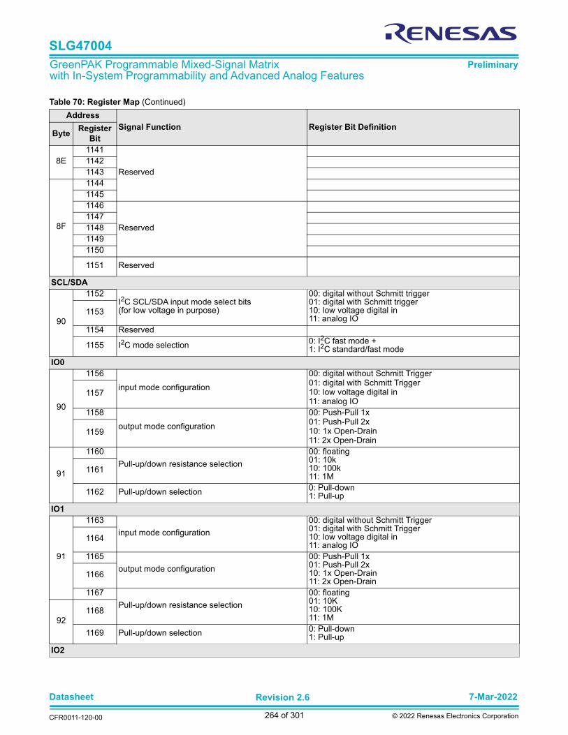
Datasheet 7-Mar-2022
CFR0011-120-00
Revision 2.6
264 of 301 © 2022 Renesas Electronics Corporation
SLG47004
GreenPAK Programmable Mixed-Signal Matrix with In-System Programmability and Advanced Analog Features
Preliminary
8E1141
Reserved11421143
8F
114411451146
Reserved1147114811491150
1151 Reserved
SCL/SDA
90
1152I2C SCL/SDA input mode select bits(for low voltage in purpose)
00: digital without Schmitt trigger01: digital with Schmitt trigger10: low voltage digital in11: analog IO
1153
1154 Reserved
1155 I2C mode selection 0: I2C fast mode +1: I2C standard/fast mode
IO0
90
1156
input mode configuration
00: digital without Schmitt Trigger01: digital with Schmitt Trigger10: low voltage digital in 11: analog IO
1157
1158
output mode configuration
00: Push-Pull 1x01: Push-Pull 2x10: 1x Open-Drain11: 2x Open-Drain
1159
91
1160
Pull-up/down resistance selection
00: floating01: 10k10: 100k 11: 1M
1161
1162 Pull-up/down selection 0: Pull-down1: Pull-up
IO1
91
1163
input mode configuration
00: digital without Schmitt Trigger01: digital with Schmitt Trigger10: low voltage digital in11: analog IO
1164
1165
output mode configuration
00: Push-Pull 1x01: Push-Pull 2x10: 1x Open-Drain 11: 2x Open-Drain
1166
1167
Pull-up/down resistance selection
00: floating01: 10K10: 100K11: 1M92
1168
1169 Pull-up/down selection 0: Pull-down1: Pull-up
IO2
Table 70: Register Map (Continued)
Address
Signal Function Register Bit DefinitionByte
Register
Bit

Datasheet 7-Mar-2022
CFR0011-120-00
Revision 2.6
265 of 301 © 2022 Renesas Electronics Corporation
SLG47004
GreenPAK Programmable Mixed-Signal Matrix with In-System Programmability and Advanced Analog Features
Preliminary
92
1170
input mode configuration
00: digital without Schmitt Trigger01: digital with Schmitt Trigger10: low voltage digital in11: analog IO
1171
1172output mode configuration
00: Push-Pull 1x01: Push-Pull 2x10: 1x Open-Drain11: 2x Open-Drain
1173
1174
Pull-up/down resistance selection
00: floating01: 10K10: 100K11: 1M
1175
93 1176 Pull-up/down selection 0: Pull-down1: Pull-up
IO3
93
1177
input mode configuration
00: digital without Schmitt Trigger01: digital with Schmitt Trigger10: low voltage digital in11: analog IO
1178
1179
output mode configuration
00: Push-Pull 1x01: Push-Pull 2x10: 1x Open-Drain11: 2x Open-Drain
1180
1181
Pull-up/down resistance selection
00: floating01: 10K10: 100K11: 1M
1182
1183 Pull-up/down selection 0: Pull-down1: Pull-up
IO4
94
1184
input mode configuration
00: digital without Schmitt Trigger01: digital with Schmitt Trigger 10: low voltage digital in11: analog IO
1185
1186
output mode configuration
00: Push-Pull 1x01: Push-Pull 2x10: 1x Open-Drain11: 2x Open-Drain
1187
1188
Pull-up/down resistance selection
00: floating01: 10K10: 100K11: 1M
1189
1190 Pull-up/down selection 0: Pull-down1: Pull-up
IO5
Table 70: Register Map (Continued)
Address
Signal Function Register Bit DefinitionByte
Register
Bit

Datasheet 7-Mar-2022
CFR0011-120-00
Revision 2.6
266 of 301 © 2022 Renesas Electronics Corporation
SLG47004
GreenPAK Programmable Mixed-Signal Matrix with In-System Programmability and Advanced Analog Features
Preliminary
94 1191
input mode configuration
00: digital without Schmitt Trigger01: digital with Schmitt Trigger10: low voltage digital in11: analog IO
95
1192
1193
output mode configuration
00: Push-Pull 1x01: Push-Pull 2x10: 1x Open-Drain 11: 2x Open-Drain
1194
1195
Pull-up/down resistance selection
00: floating 01: 10K10: 100K11: 1M
1196
1197 Pull-up/down selection 0: Pull-down1: Pull-up
IO6
95
1198
input mode configuration
00: digital without Schmitt Trigger01: digital with Schmitt Trigger10: low voltage digital in11: analog IO
1199
96
1200
output mode configuration
00: Push-Pull 1x01: Push-Pull 2x10: 1x Open-Drain11: 2x Open-Drain
1201
1202
Pull-up/down resistance selection
00: floating01: 10K10: 100K11: 1M
1203
1204 Pull-up/down selection 0: Pull-down1: Pull-up
I0
96
1205
input mode configuration
00: digital without Schmitt Trigger01: digital with Schmitt Trigger10: low voltage digital in11: analog IO
1206
1207 IO fast Pull-up/down enable 0: disable1: enable
97
1208 Reserved1209 Reserved1210 Reserved1211 Reserved1212 Reserved1213 Reserved1214 Reserved1215 Reserved
Table 70: Register Map (Continued)
Address
Signal Function Register Bit DefinitionByte
Register
Bit

Datasheet 7-Mar-2022
CFR0011-120-00
Revision 2.6
267 of 301 © 2022 Renesas Electronics Corporation
SLG47004
GreenPAK Programmable Mixed-Signal Matrix with In-System Programmability and Advanced Analog Features
Preliminary
98
1216
Multi0 register configure
mulit_function selection12171218
dly2lut selection1219
1220output selection of LUT4_1/DFF17:0: LUT4_11: DFF17
1221external clock selection
12221223
DLY/CNT0 Mode Selection
00: DLY01: one shoot10: frequency detect 11: CNT register [1238] = 0
99
1224
1225
DLY/CNT0 edge Mode Selection
00: both edge01: falling edge 10: rising edge11: High Level Reset (only in CNT mode)
1226
1227
DLY/CNT0 Clock Source Select
Clock source sel[3:0]0000: 25M(OSC2)0001: 25M/40010: 2M(OSC1)0011: 2M/80100: 2M/640101: 2M/5120110: 2K(OSC0)0111: 2K/81000: 2K/641001: 2K/5121010: 2K/40961011: 2K/327681100: 2K/2621441101: CNT6_END1110: External1111: Not used
12281229
1230
1231 FSM0 SET/RST Selection 0: Reset to 01: Set to data
9A
1232 wake sleep mode selection0: Default Mode, 1: Wake Sleep Mode(registers [1224:1223] = 11)
1233 Wake sleep power down state selection 0: low1: high
1234 Keep signal sync selection 0: bypass1: after two DFF
1235 UP signal sync selection 0: bypass 1: after two DFF
1236 CNT0 CNT mode SYNC selection 0: bypass1: after two DFF
1237 CNT0 output pol selection 0: Default Output1: Inverted Output
1238 CNT0 DLY EDET FUNCTION Selection0: normal1: DLY function edge detection (registers [1224:1223] = 00)
1239 Reserved
Table 70: Register Map (Continued)
Address
Signal Function Register Bit DefinitionByte
Register
Bit

Datasheet 7-Mar-2022
CFR0011-120-00
Revision 2.6
268 of 301 © 2022 Renesas Electronics Corporation
SLG47004
GreenPAK Programmable Mixed-Signal Matrix with In-System Programmability and Advanced Analog Features
Preliminary
9B
1240
Multi1 register configure
mulit_function selection12411242
dly2lut selection1243
1244output selection of LUT3_7/DFF11: 0: LUT3_71: DFF11
1245 CNT1 DLY EDET FUNCTION Selection0: normal1: DLY function edge detection(registers [1251:1248] = 0000/0001/0010)
1246 CNT1 CNT mode SYNC selection 0: bypass1: after two DFF
1247 CNT1 output pol selection 0: Default Output1: Inverted Output
9C
1248
CNT1 function and edge mode selection
0000: both edge Delay0001: falling edge delay0010: rising edge delay0011: both edge One Shot 0100: falling edge One Shot 0101: rising edge One Shot 0110: both edge freq detect 0111: falling edge freq detect1000: rising edge freq detect 1001: both edge detect1010: falling edge detect1011: rising edge detect1100: both edge reset CNT1101: falling edge reset CNT1110: rising edge reset CNT1111: high level reset CNT
12491250
1251
1252
DLY/CNT1 Clock Source Select
Clock source sel[3:0]0000: 25M(OSC2)0001: 25M/40010: 2M(OSC1)0011: 2M/80100: 2M/640101: 2M/5120110: 2K(OSC0)0111: 2K/81000: 2K/641001: 2K/5121010: 2K/40961011: 2K/327681100: 2K/2621441101: CNT0_END1110: External1111: Not used
12531254
1255
Table 70: Register Map (Continued)
Address
Signal Function Register Bit DefinitionByte
Register
Bit

Datasheet 7-Mar-2022
CFR0011-120-00
Revision 2.6
269 of 301 © 2022 Renesas Electronics Corporation
SLG47004
GreenPAK Programmable Mixed-Signal Matrix with In-System Programmability and Advanced Analog Features
Preliminary
9D
1256
Multi2 register configure
mulit_function selection12571258
dly2lut selection1259
1260output selection of LUT3_8/DFF12: 0: LUT3_81: DFF12
1261 CNT2 DLY EDET FUNCTION Selection0: normal1: DLY function edge detection (registers [1267:1264] = 0000/0001/0010)
1262 CNT2 CNT mode SYNC selection 0: bypass1: after two DFF
1263 CNT2 output pol selection 0: Default Output1: Inverted Output
9E
1264
CNT2 function and edge mode selection
0000: both edge Delay0001: falling edge delay0010: rising edge delay0011: both edge One Shot0100: falling edge One Shot0101: rising edge One Shot0110: both edge freq detect0111: falling edge freq detect1000: rising edge freq detect1001: both edge detect1010: falling edge detect1011: rising edge detect1100: both edge reset CNT1101: falling edge reset CNT 1110: rising edge reset CNT111: high level reset CNT
12651266
1267
9E
1268
DLY/CNT2 Clock Source Select
Clock source sel[3:0]0000: 25M(OSC2)0001: 25M/40010: 2M(OSC1)0011: 2M/80100: 2M/640101: 2M/5120110: 2K(OSC0)0111: 2K/81000: 2K/641001: 2K/5121010: 2K/40961011: 2K/32768 1100: 2K/2621441101: CNT1_END1110: External1111: Not used
12691270
1271
Table 70: Register Map (Continued)
Address
Signal Function Register Bit DefinitionByte
Register
Bit

Datasheet 7-Mar-2022
CFR0011-120-00
Revision 2.6
270 of 301 © 2022 Renesas Electronics Corporation
SLG47004
GreenPAK Programmable Mixed-Signal Matrix with In-System Programmability and Advanced Analog Features
Preliminary
9F
1272
Multi3 register configure
mulit_function selection12731274
dly2lut selection1275
1276output selection of LUT3_9/DFF13: 0: LUT3_9 1: DFF13
1277 CNT3 DLY EDET FUNCTION Selection0: normal1: DLY function edge detection(registers [1283:1280] = 0000/0001/0010)
1278 CNT3 CNT mode SYNC selection 0: bypass; 1: after two DFF
1279 CNT3 output pol selection 0: Default Output, 1: Inverted Output
A0
1280
CNT3 function and edge mode selection
0000: both edge Delay0001: falling edge delay0010: rising edge delay0011: both edge One Shot0100: falling edge One Shot0101: rising edge One Shot0110: both edge freq detect0111: falling edge freq detect 1000: rising edge freq detect1001: both edge detect1010: falling edge detect1011: rising edge detect1100: both edge reset CNT1101: falling edge reset CNT1110: rising edge reset CNT1111: high level reset CNT
12811282
1283
1284
DLY/CNT3 Clock Source Select
Clock source sel[3:0]0000: 25M(OSC2)0001: 25M/40010: 2M(OSC1)0011: 2M/80100: 2M/640101: 2M/5120110: 2K(OSC0)0111: 2K/81000: 2K/641001: 2K/5121010: 2K/40961011: 2K/327681100: 2K/2621441101: CNT2_END1110: External1111: Not used
12851286
1287
Table 70: Register Map (Continued)
Address
Signal Function Register Bit DefinitionByte
Register
Bit

Datasheet 7-Mar-2022
CFR0011-120-00
Revision 2.6
271 of 301 © 2022 Renesas Electronics Corporation
SLG47004
GreenPAK Programmable Mixed-Signal Matrix with In-System Programmability and Advanced Analog Features
Preliminary
A1
1288
Multi4 register configure
mulit_function selection12891290
dly2lut selection1291
1292output selection of LUT3_10/DFF14:0: LUT3_101: DFF14
1293 CNT4 DLY EDET FUNCTION Selection0: normal1: DLY function edge detection (registers [1299:1296] = 0000/0001/0010)
1294 CNT4 CNT mode SYNC selection 0: bypass1: after two DFF
1295 CNT4 output pol selection 0: Default Output1: Inverted Output
A2
1296
CNT4 function and edge mode selection
0000: both edge Delay0001: falling edge delay0010: rising edge delay0011: both edge One Shot0100: falling edge One Shot 0101: rising edge One Shot 0110: both edge freq detect;0111: falling edge freq detect 1000: rising edge freq detect1001: both edge detect 1010: falling edge detect1011: rising edge detect1100: both edge reset CNT1101: falling edge reset CNT1110: rising edge reset CNT1111: high level reset CNT
12971298
1299
1300
DLY/CNT4 Clock Source Select
Clock source sel[3:0]0000: 25M(OSC2)0001: 25M/40010: 2M(OSC1)0011: 2M/80100: 2M/640101: 2M/5120110: 2K(OSC0)0111: 2K/81000: 2K/641001: 2K/5121010: 2K/40961011: 2K/327681100: 2K/2621441101: CNT3_END1110: External1111: Not used
13011302
1303
Table 70: Register Map (Continued)
Address
Signal Function Register Bit DefinitionByte
Register
Bit

Datasheet 7-Mar-2022
CFR0011-120-00
Revision 2.6
272 of 301 © 2022 Renesas Electronics Corporation
SLG47004
GreenPAK Programmable Mixed-Signal Matrix with In-System Programmability and Advanced Analog Features
Preliminary
A3
1304
Multi5 register configure
mulit_function selection13051306
dly2lut selection1307
1308output selection of LUT3_11/DFF15:0: LUT3_111: DFF15
1309 CNT5 DLY EDET FUNCTION Selection0: normal1: DLY function edge detection (registers [1315:1312] = 0000/0001/0010)
1310 CNT5 CNT mode SYNC selection 0: bypass1: after two DFF
1311 CNT5 output pol selection 0: Default Output1: Inverted Output
A4
1312
CNT5 function and edge mode selection
0000: both edge Delay0001: falling edge delay0010: rising edge delay0011: both edge One Shot 0100: falling edge One Shot0101: rising edge One Shot0110: both edge freq detect0111: falling edge freq detect 1000: rising edge freq detect 1001: both edge detect1010: falling edge detect1011: rising edge detect1100: both edge reset CNT1101: falling edge reset CNT1110: rising edge reset CNT1111: high level reset CNT
13131314
1315
1316
DLY/CNT5 Clock Source Select
Clock source sel[3:0]0000: 25M(OSC2)0001: 25M/40010: 2M(OSC1)0011: 2M/80100: 2M/640101: 2M/5120110: 2K(OSC0)0111: 2K/81000: 2K/641001: 2K/5121010: 2K/40961011: 2K/327681100: 2K/2621441101: CNT4_END1110: External1111: Not used
13171318
1319
Table 70: Register Map (Continued)
Address
Signal Function Register Bit DefinitionByte
Register
Bit
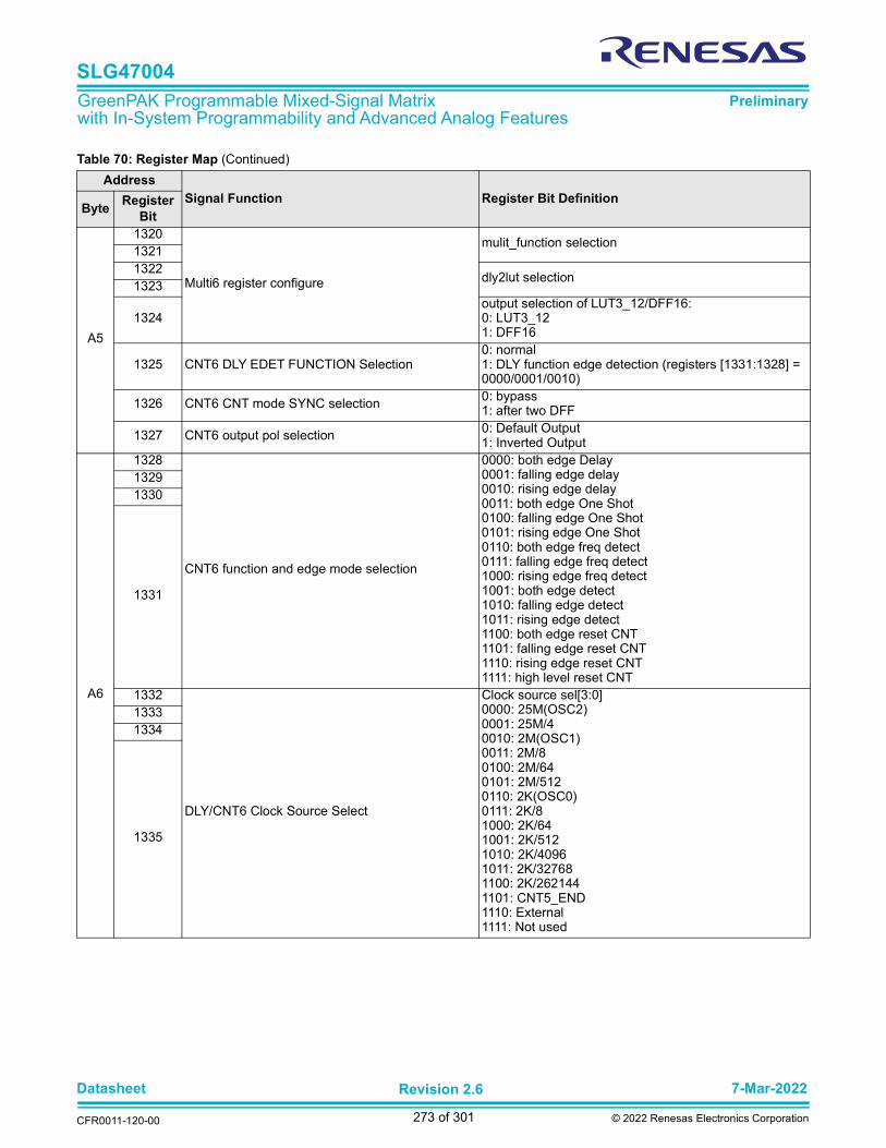
Datasheet 7-Mar-2022
CFR0011-120-00
Revision 2.6
273 of 301 © 2022 Renesas Electronics Corporation
SLG47004
GreenPAK Programmable Mixed-Signal Matrix with In-System Programmability and Advanced Analog Features
Preliminary
A5
1320
Multi6 register configure
mulit_function selection13211322
dly2lut selection1323
1324output selection of LUT3_12/DFF16:0: LUT3_121: DFF16
1325 CNT6 DLY EDET FUNCTION Selection0: normal1: DLY function edge detection (registers [1331:1328] = 0000/0001/0010)
1326 CNT6 CNT mode SYNC selection 0: bypass1: after two DFF
1327 CNT6 output pol selection 0: Default Output1: Inverted Output
A6
1328
CNT6 function and edge mode selection
0000: both edge Delay0001: falling edge delay0010: rising edge delay0011: both edge One Shot 0100: falling edge One Shot0101: rising edge One Shot 0110: both edge freq detect0111: falling edge freq detect1000: rising edge freq detect 1001: both edge detect1010: falling edge detect1011: rising edge detect1100: both edge reset CNT1101: falling edge reset CNT1110: rising edge reset CNT1111: high level reset CNT
13291330
1331
1332
DLY/CNT6 Clock Source Select
Clock source sel[3:0]0000: 25M(OSC2)0001: 25M/40010: 2M(OSC1)0011: 2M/80100: 2M/64 0101: 2M/5120110: 2K(OSC0)0111: 2K/81000: 2K/641001: 2K/5121010: 2K/40961011: 2K/327681100: 2K/2621441101: CNT5_END1110: External1111: Not used
13331334
1335
Table 70: Register Map (Continued)
Address
Signal Function Register Bit DefinitionByte
Register
Bit
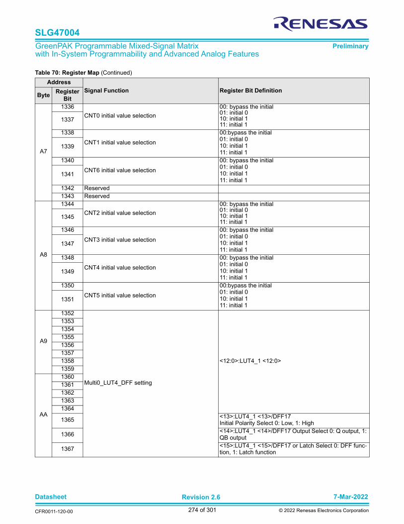
Datasheet 7-Mar-2022
CFR0011-120-00
Revision 2.6
274 of 301 © 2022 Renesas Electronics Corporation
SLG47004
GreenPAK Programmable Mixed-Signal Matrix with In-System Programmability and Advanced Analog Features
Preliminary
A7
1336
CNT0 initial value selection
00: bypass the initial01: initial 010: initial 111: initial 1
1337
1338
CNT1 initial value selection
00:bypass the initial01: initial 010: initial 111: initial 1
1339
1340
CNT6 initial value selection
00: bypass the initial01: initial 010: initial 111: initial 1
1341
1342 Reserved1343 Reserved
A8
1344
CNT2 initial value selection
00: bypass the initial01: initial 010: initial 111: initial 1
1345
1346
CNT3 initial value selection
00: bypass the initial01: initial 010: initial 111: initial 1
1347
1348
CNT4 initial value selection
00: bypass the initial01: initial 010: initial 111: initial 1
1349
1350
CNT5 initial value selection
00:bypass the initial01: initial 010: initial 111: initial 1
1351
A9
1352
Multi0_LUT4_DFF setting
<12:0>:LUT4_1 <12:0>
1353135413551356135713581359
AA
13601361136213631364
1365 <13>:LUT4_1 <13>/DFF17Initial Polarity Select 0: Low, 1: High
1366 <14>:LUT4_1 <14>/DFF17 Output Select 0: Q output, 1: QB output
1367 <15>:LUT4_1 <15>/DFF17 or Latch Select 0: DFF func-tion, 1: Latch function
Table 70: Register Map (Continued)
Address
Signal Function Register Bit DefinitionByte
Register
Bit

Datasheet 7-Mar-2022
CFR0011-120-00
Revision 2.6
275 of 301 © 2022 Renesas Electronics Corporation
SLG47004
GreenPAK Programmable Mixed-Signal Matrix with In-System Programmability and Advanced Analog Features
Preliminary
AB
1368
REG_CNT0_D<15:0> Data[15:0]
1369137013711372137313741375
AC
13761377137813791380138113821383
AD
1384
Multi1_LUT3_DFF setting
<3:0>:LUT3_7 <3:0>138513861387
1388 <4>:LUT3_7 <4>/DFF11 Initial Polarity Select0: Low, 1: High
1389 <5>:LUT3_7 <5>/DFF110: RSTB from Matrix Output, 1: SETB from Matrix Output
1390 <6>:LUT3_7 <6>/DFF11 Output Select0: Q output, 1: QB output
1391 <7>:LUT3_7 <7>/DFF11 or Latch Select0: DFF function, 1: Latch function
Multi1_CNT1
AE
1392
REG_CNT1_D<7:0> Data[7:0]
1393139413951396139713981399
AF
1400
Multi2_LUT3_DFF setting
<3:0>:LUT3_8 <3:0>140114021403
1404 <4>:LUT3_8 <4>/DFF12 Initial Polarity Select0: Low, 1: High
1405 <5>:LUT3_8 <5>/DFF120: RSTB from Matrix Output, 1: SETB from Matrix Output
1406 <6>:LUT3_8 <6>/DFF12 Output Select0: Q output, 1: QB output
1407 <7>:LUT3_8 <7>/DFF12 or Latch Select0: DFF function, 1: Latch function
Table 70: Register Map (Continued)
Address
Signal Function Register Bit DefinitionByte
Register
Bit

Datasheet 7-Mar-2022
CFR0011-120-00
Revision 2.6
276 of 301 © 2022 Renesas Electronics Corporation
SLG47004
GreenPAK Programmable Mixed-Signal Matrix with In-System Programmability and Advanced Analog Features
Preliminary
B0
1408
REG_CNT2_D<7:0> Data[7:0]
1409141014111412141314141415
B1
1416
Multi3_LUT3_DFF setting
<3:0>:LUT3_9 <3:0>141714181419
1420 <4>:LUT3_9 <4>/DFF13 Initial Polarity Select0: Low, 1: High
1421 <5>:LUT3_9 <5>/DFF130: RSTB from Matrix Output, 1: SETB from Matrix Output
1422 <6>:LUT3_9 <6>/DFF13 Output Select0: Q output, 1: QB output
1423 <7>:LUT3_9 <7>/DFF13 or Latch Select0: DFF function, 1: Latch function
B2
1424
REG_CNT3_D<7:0> Data[7:0]
1425142614271428142914301431
B3
1432
Multi4_LUT3_DFF setting
<3:0>:LUT3_10 <3:0>143314341435
1436 <4>:LUT3_10 <4>/DFF14 Initial Polarity Select0: Low, 1: High
1437 <5>:LUT3_10 <5>/DFF140: RSTB from Matrix Output, 1: SETB from Matrix Output
1438 <6>:LUT3_10 <6>/DFF14 Output Select0: Q output, 1: QB output
1439 <7>:LUT3_10 <7>/DFF14 or Latch Select0: DFF function, 1: Latch function
B4
1440
REG_CNT4_D<7:0> Data[7:0]
1441144214431444144514461447
Table 70: Register Map (Continued)
Address
Signal Function Register Bit DefinitionByte
Register
Bit

Datasheet 7-Mar-2022
CFR0011-120-00
Revision 2.6
277 of 301 © 2022 Renesas Electronics Corporation
SLG47004
GreenPAK Programmable Mixed-Signal Matrix with In-System Programmability and Advanced Analog Features
Preliminary
B5
1448
Multi5_LUT3_DFF setting
<3:0>:LUT3_11<3:0>144914501451
1452 <4>:LUT3_11<4>/DFF15 Initial Polarity Select0: Low, 1: High
1453 <5>:LUT3_11 <5>/DFF150: RSTB from Matrix Output, 1: SETB from Matrix Output
1454 <6>:LUT3_11 <6>/DFF15 Output Select0: Q output, 1: QB output
1455 <7>:LUT3_11 <7>/DFF15 or Latch Select0: DFF function, 1: Latch function
B6
1456
REG_CNT5_D<7:0> Data[7:0]
1457145814591460146114621463
B7
1464
Multi6_LUT3_DFF setting
<3:0>:LUT3_12 <3:0>146514661467
1468 <4>:LUT3_12 <4>/DFF16 Initial Polarity Select0: Low, 1: High
1469 <5>:LUT3_12 <5>/DFF160: RSTB from Matrix Output, 1: SETB from Matrix Output
1470 <6>:LUT3_12 <6>/DFF16 Output Select0: Q output, 1: QB output
1471 <7>:LUT3_12 <7>/DFF16 or Latch Select0: DFF function, 1: Latch function
B8
1472
REG_CNT6_D<7:0> Data[7:0]
1473147414751476147714781479
Table 70: Register Map (Continued)
Address
Signal Function Register Bit DefinitionByte
Register
Bit

Datasheet 7-Mar-2022
CFR0011-120-00
Revision 2.6
278 of 301 © 2022 Renesas Electronics Corporation
SLG47004
GreenPAK Programmable Mixed-Signal Matrix with In-System Programmability and Advanced Analog Features
Preliminary
B9
1480
LUT2_0/DFF0 setting
<0>:LUT2_0 <0>
1481 <1>:LUT2_0 <1>/DFF0 Initial Polarity Select0: Low, 1: High
1482 <2>:LUT2_0 <2>/DFF0 Output Select0: Q output, 1: QB output
1483 <3>:LUT2_0 <3>/DFF0 or Latch Select0: DFF function, 1: Latch function
1484
LUT2_1/DFF1 setting
<0>:LUT2_0 <0>
1485 <1>:LUT2_0 <1>/DFF0 Initial Polarity Select 0: Low, 1: High
1486 <2>:LUT2_0 <2>/DFF0 Output Select 0: Q output, 1: QB output
1487 <3>:LUT2_0 <3>/DFF0 or Latch Select 0: DFF function, 1: Latch function
BA
1488
LUT2_2/DFF2 setting
<0>:LUT2_0 <0>
1489 <1>:LUT2_0 <1>/DFF0 Initial Polarity Select 0: Low, 1: High
1490 <2>:LUT2_0 <2>/DFF0 Output Select 0: Q output, 1: QB output
1491 <3>:LUT2_0 <3>/DFF0 or Latch Select 0: DFF function, 1: Latch function
1492 LUT2_0 or DFF0 Select 0: LUT2_01: DFF0
1493 LUT2_1 or DFF1 Select 0: LUT2_11: DFF1
1494 LUT2_2 or DFF2 Select 0: LUT2_21: DFF2
1495 Reserved
BB
1496
PGen data PGen Data[15:0]
1497149814991500150115021503
BC
15041505150615071508150915101511
Table 70: Register Map (Continued)
Address
Signal Function Register Bit DefinitionByte
Register
Bit

Datasheet 7-Mar-2022
CFR0011-120-00
Revision 2.6
279 of 301 © 2022 Renesas Electronics Corporation
SLG47004
GreenPAK Programmable Mixed-Signal Matrix with In-System Programmability and Advanced Analog Features
Preliminary
BD
1512
LUT2_3_VAL or PGen_data LUT2_3<3:0> or PGen 4bit counterdata<3:0>
151315141515
1516 LUT2_3 or PGen Select 0: LUT2_31: PGen
1517 Active level selection for RST/SET 0: Active low level reset/set1: Active high level reset/set
1518 LUT3_0 or DFF3 Select 0: LUT3_01: DFF3
1519 LUT3_1 or DFF4 Select 0: LUT3_11: DFF4
BE
1520
LUT3_0_DFF3 setting
<1:0>: LUT3_0 <1:0>1521
1522 <2>:LUT3_0 <2>/DFF3 stage selection 0: Q of first DFF; 1 Q of second DFF
1523
<3>:LUT3_0 <3>/DFF3 Active level selection for RST/SET 0: Active low level reset/set, 1: Active high level reset/set
1524<4>:LUT3_0 <4>/DFF3 0: RSTB from Matrix Output, 1: SETB from Matrix Output
1525 <5>:LUT3_0 <5>/DFF3 Initial Polarity Select 0: Low, 1: High
1526 <6>:LUT3_0 <6>/DFF3 Output Select 0: Q output, 1: QB output
1527 <7>:LUT3_0 <7>/DFF3 or Latch Select 0: DFF function, 1: Latch function
BF
1528
LUT3_1_DFF4 setting
<2:0>: LUT3_1 <2:0>15291530
1531
<3>:LUT3_1 <3>/DFF4 Active level selection for RST/SET 0: Active low level reset/set, 1: Active high level reset/set
1532<4>:LUT3_1 <4>/DFF4 0: RSTB from Matrix Output, 1: SETB from Matrix Output
1533 <5>:LUT3_1 <5>/DFF4 Initial Polarity Select 0: Low, 1: High
1534 <6>:LUT3_1 <6>/DFF4 Output Select 0: Q output, 1: QB output
1535 <7>:LUT3_1 <7>/DFF4 or Latch Select 0: DFF function, 1: Latch function
Table 70: Register Map (Continued)
Address
Signal Function Register Bit DefinitionByte
Register
Bit

Datasheet 7-Mar-2022
CFR0011-120-00
Revision 2.6
280 of 301 © 2022 Renesas Electronics Corporation
SLG47004
GreenPAK Programmable Mixed-Signal Matrix with In-System Programmability and Advanced Analog Features
Preliminary
C0
1536
Rheostat0 data selection 0000000000: 0~1111111111:100k
1537153815391540154115421543
C1
154415451546 Reserved1547 Reserved1548 Reserved1549 Reserved1550 Reserved1551 Reserved
C2
1552
Rheostat0 current value (read only)
1553155415551556155715581559
C3
156015611562 Reserved1563 Reserved1564 Reserved1565 Reserved1566 Reserved1567 Reserved
C4
1568 Matrix Input 0 GND1569 Matrix Input 1 LUT2_0/DFF0 output1570 Matrix Input 2 LUT2_1/DFF1 output1571 Matrix Input 3 LUT2_2/DFF2 output1572 Matrix Input 4 LUT2_3/PGen output1573 Matrix Input 5 LUT3_0/DFF3 output1574 Matrix Input 6 LUT3_1/DFF4 output1575 Matrix Input 7 LUT3_2/DFF5 output
C5
1576 Matrix Input 8 LUT3_3/DFF6 output1577 Matrix Input 9 LUT3_4/DFF7 output1578 Matrix Input 10 LUT3_5/DFF8 output1579 Matrix Input 11 LUT3_6/DFF9 output1580 Matrix Input 12 CNT_DLY0 output1581 Matrix Input 13 MLT0_LUT4_1/DFF17_OUT1582 Matrix Input 14 CNT_DLY1 output1583 Matrix Input 15 MLT1_LUT3_7/DFF11_OUT
Table 70: Register Map (Continued)
Address
Signal Function Register Bit DefinitionByte
Register
Bit

Datasheet 7-Mar-2022
CFR0011-120-00
Revision 2.6
281 of 301 © 2022 Renesas Electronics Corporation
SLG47004
GreenPAK Programmable Mixed-Signal Matrix with In-System Programmability and Advanced Analog Features
Preliminary
C6
1584 Matrix Input 16 CNT_DLY2 output1585 Matrix Input 17 MLT2_LUT3_8/DFF12_OUT1586 Matrix Input 18 CNT_DLY3 output1587 Matrix Input 19 MLT3_LUT3_9/DFF13_OUT1588 Matrix Input 20 CNT_DLY4 output1589 Matrix Input 21 MLT4_LUT3_10/DFF14_OUT1590 Matrix Input 22 CNT_DLY5 output1591 Matrix Input 23 MLT5_LUT3_11/DFF15_OUT
C7
1592 Matrix Input 24 CNT_DLY6 output1593 Matrix Input 25 MLT6_LUT3_12/DFF16_OUT1594 Matrix Input 26 LUT3_13/Pipe Delay/RippleCNT_out01595 Matrix Input 27 Pipe Delay/RippleCNT_out11596 Matrix Input 28 Pipe Delay/RippleCNT_out21597 Matrix Input 29 LUT4_0/DFF10 output1598 Matrix Input 30 Programmable Delay Edge Detect Output1599 Matrix Input 31 Edge Detect Filter Output
C8
1600 Matrix Input 40 RH0 Idle/Active1601 Matrix Input 41 RH1 Idle/Active1602 Matrix Input 42 Output of Op Amp0 in ACMP mode1603 Matrix Input 43 Output of Op Amp1 in ACMP mode1604 Matrix Input 44 IO0 Digital Input1605 Matrix Input 45 IO1 Digital Input1606 Matrix Input 46 IO2 Digital Input1607 Matrix Input 47 IO3 Digital Input
C9
1608 Matrix Input 48 IO4 Digital Input1609 Matrix Input 49 IO5 Digital Input1610 Matrix Input 50 IO6 Digital Input1611 Matrix Input 51 I0 Digital Input1612 Matrix Input 52 Oscillator0 output 01613 Matrix Input 53 Oscillator1 output 01614 Matrix Input 54 Oscillator2 output1615 Matrix Input 55 Chopper ACMP Out
CA
1616 Matrix Input 56 ACMP0 Output (low speed)1617 Matrix Input 57 ACMP1 Output (low speed)1618 Matrix Input 58 Oscillator0 output 11619 Matrix Input 59 Oscillator1 output 11620 Matrix Input 60 POR OUT1621 Matrix Input 61 VDD1622 Matrix Input 62 VDD1623 Matrix Input 63 VDD
Table 70: Register Map (Continued)
Address
Signal Function Register Bit DefinitionByte
Register
Bit
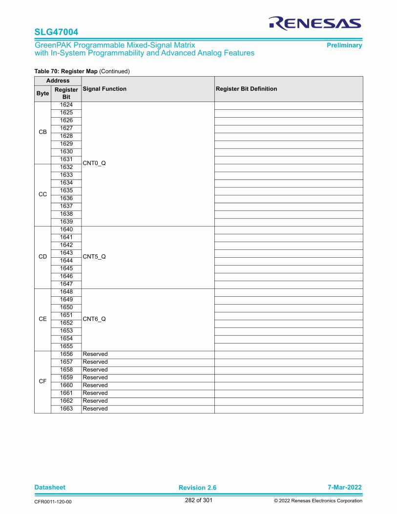
Datasheet 7-Mar-2022
CFR0011-120-00
Revision 2.6
282 of 301 © 2022 Renesas Electronics Corporation
SLG47004
GreenPAK Programmable Mixed-Signal Matrix with In-System Programmability and Advanced Analog Features
Preliminary
CB
1624
CNT0_Q
1625162616271628162916301631
CC
16321633163416351636163716381639
CD
1640
CNT5_Q
1641164216431644164516461647
CE
1648
CNT6_Q
1649165016511652165316541655
CF
1656 Reserved1657 Reserved1658 Reserved1659 Reserved1660 Reserved1661 Reserved1662 Reserved1663 Reserved
Table 70: Register Map (Continued)
Address
Signal Function Register Bit DefinitionByte
Register
Bit
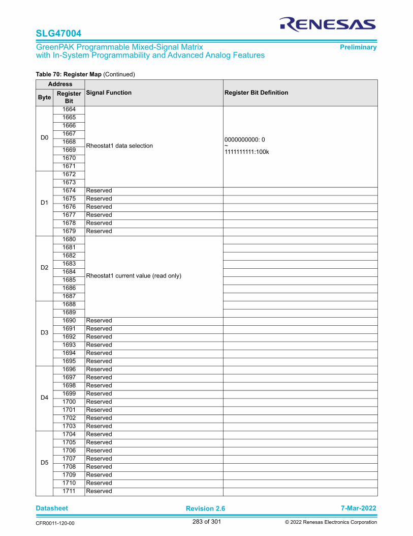
Datasheet 7-Mar-2022
CFR0011-120-00
Revision 2.6
283 of 301 © 2022 Renesas Electronics Corporation
SLG47004
GreenPAK Programmable Mixed-Signal Matrix with In-System Programmability and Advanced Analog Features
Preliminary
D0
1664
Rheostat1 data selection0000000000: 0~1111111111:100k
1665166616671668166916701671
D1
167216731674 Reserved1675 Reserved1676 Reserved1677 Reserved1678 Reserved1679 Reserved
D2
1680
Rheostat1 current value (read only)
1681168216831684168516861687
D3
168816891690 Reserved1691 Reserved1692 Reserved1693 Reserved1694 Reserved1695 Reserved
D4
1696 Reserved1697 Reserved1698 Reserved1699 Reserved1700 Reserved1701 Reserved1702 Reserved1703 Reserved
D5
1704 Reserved1705 Reserved1706 Reserved1707 Reserved1708 Reserved1709 Reserved1710 Reserved1711 Reserved
Table 70: Register Map (Continued)
Address
Signal Function Register Bit DefinitionByte
Register
Bit

Datasheet 7-Mar-2022
CFR0011-120-00
Revision 2.6
284 of 301 © 2022 Renesas Electronics Corporation
SLG47004
GreenPAK Programmable Mixed-Signal Matrix with In-System Programmability and Advanced Analog Features
Preliminary
D6
1712 Reserved1713 Reserved1714 Reserved1715 Reserved1716 Reserved1717 Reserved1718 Reserved1719 Reserved
D7
1720 Reserved1721 Reserved1722 Reserved1723 Reserved1724 Reserved1725 Reserved1726 Reserved1727 Reserved
D8
1728 Reserved1729 Reserved1730 Reserved1731 Reserved1732 Reserved1733 Reserved1734 Reserved1735 Reserved
D9
1736 Reserved1737 Reserved1738 Reserved1739 Reserved1740 Reserved1741 Reserved1742 Reserved1743 Reserved
DA
1744 Reserved1745 Reserved1746 Reserved1747 Reserved1748 Reserved1749 Reserved1750 Reserved1751 Reserved
DB
1752 Reserved1753 Reserved1754 Reserved1755 Reserved1756 Reserved1757 Reserved1758 Reserved1759 Reserved
Table 70: Register Map (Continued)
Address
Signal Function Register Bit DefinitionByte
Register
Bit
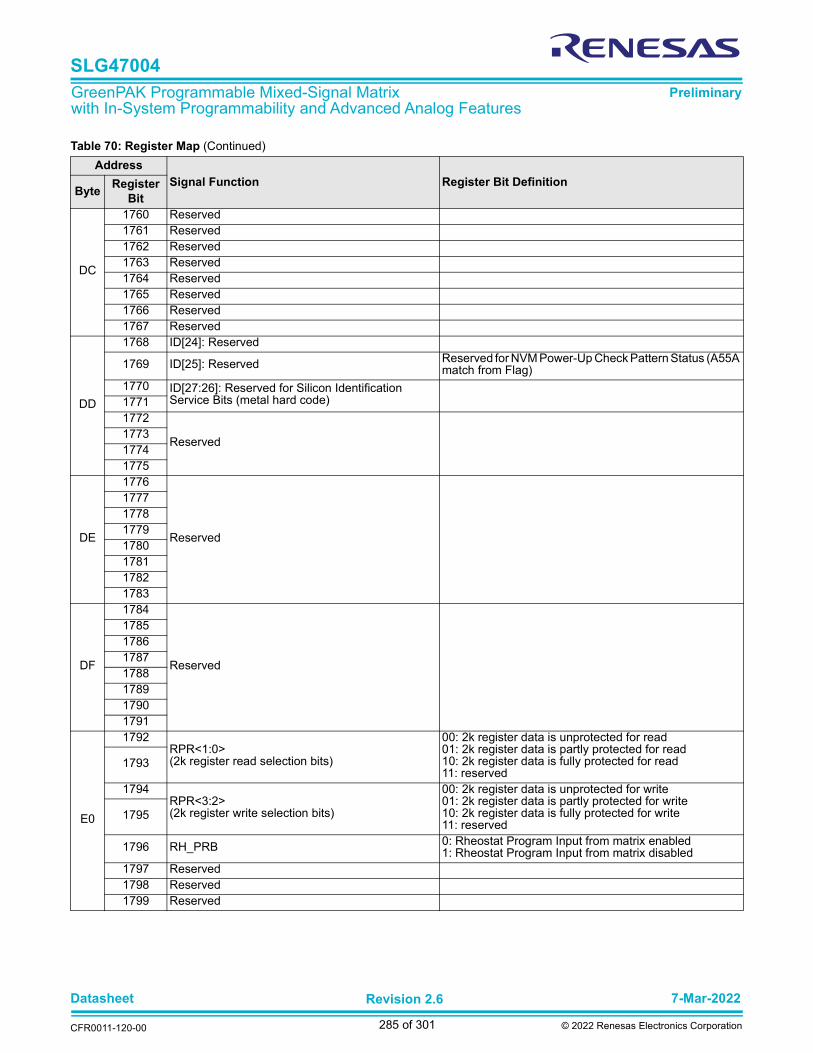
Datasheet 7-Mar-2022
CFR0011-120-00
Revision 2.6
285 of 301 © 2022 Renesas Electronics Corporation
SLG47004
GreenPAK Programmable Mixed-Signal Matrix with In-System Programmability and Advanced Analog Features
Preliminary
DC
1760 Reserved1761 Reserved1762 Reserved1763 Reserved1764 Reserved1765 Reserved1766 Reserved1767 Reserved
DD
1768 ID[24]: Reserved
1769 ID[25]: Reserved Reserved for NVM Power-Up Check Pattern Status (A55A match from Flag)
1770 ID[27:26]: Reserved for Silicon IdentificationService Bits (metal hard code)1771
1772
Reserved177317741775
DE
1776
Reserved
1777177817791780178117821783
DF
1784
Reserved
1785178617871788178917901791
E0
1792RPR<1:0>(2k register read selection bits)
00: 2k register data is unprotected for read01: 2k register data is partly protected for read10: 2k register data is fully protected for read11: reserved
1793
1794RPR<3:2>(2k register write selection bits)
00: 2k register data is unprotected for write01: 2k register data is partly protected for write10: 2k register data is fully protected for write11: reserved
1795
1796 RH_PRB 0: Rheostat Program Input from matrix enabled1: Rheostat Program Input from matrix disabled
1797 Reserved1798 Reserved1799 Reserved
Table 70: Register Map (Continued)
Address
Signal Function Register Bit DefinitionByte
Register
Bit

Datasheet 7-Mar-2022
CFR0011-120-00
Revision 2.6
286 of 301 © 2022 Renesas Electronics Corporation
SLG47004
GreenPAK Programmable Mixed-Signal Matrix with In-System Programmability and Advanced Analog Features
Preliminary
E1
1800
NPR<1:0>(2k NVM configuration selection bits)
00: 2k NVM Configuration data is unprotected for read and write/erase01: 2k NVM Configuration data is fully protected for read10: 2k NVM Configuration data is fully protected for write/erase11: 2k NVM Configuration data is fully protected for read and write/erase
1801
1802
NPR<3:2>(Rheostat0 NVM configuration selection bits)
00: Rheosta0 NVM Configuration data is unprotected for read and write/erase01: Rheosta0 NVM Configuration data is fully protected for read10: Rheosta0 NVM Configuration data is fully protected for write/erase11: Rheosta0 NVM Configuration data is fully protected for read and write/erase
1803
1804
NPR<5:4>(Rheostat1 NVM configuration selection bits)
00: Rheosta1 NVM Configuration data is unprotected for read and write/erase01: Rheosta1 NVM Configuration data is fully protected for read10: Rheosta1 NVM Configuration data is fully protected for write/erase11: Rheosta1 NVM Configuration data is fully protected for read and write/erase
1805
1806 Reserved1807 Reserved
E2
1808WPR<1:0>(EEPROM Write protect block bitsrange: page31~16)
00: Upper 1/4 (page16~19) of EEPROM is write protected (default)01: Upper 2/4 (page16~23) of EEPROM is write protected10: Upper 3/4 (page16~27) of EEPROM is write protected11: Entire (page16~31) EEPROM is write protected
1809
1810 WPRE(EEPROM Write protect register enable)
0: No Software Write Protection enabled (default)1: Write Protection is set by the state of the WPR<1:0> bits
1811 Reserved1812 Reserved1813 Reserved1814 Reserved1815 Reserved
E3
1816
ERSE<4:0>(Page selection for erase)
Define the page address which will be erasedERSE<4> = 0 corresponds to the upper 2k NVM used for chip configurationERSE<4> = 1 corresponds to the 2kEEPROM
18171818181918201821
ERSE <2:0>(Erase enable)
000/001/010/011/100/101/111: erase disable110: cause the NVM erase: full NVM (4k bits) erase for ERSCHIP = 1 if DIS_ERSCHIP=0 or page erase forERSCHIP=0.
1822
1823
E4
1824 PRL(Protection lock)
0: RPR/WPR/NPR setting can be changed1: RPR/WPR/NPR setting cannot be changed
1825 Reserved1826 Reserved1827 Reserved1828 Reserved1829 Reserved1830 Reserved1831 Reserved
Table 70: Register Map (Continued)
Address
Signal Function Register Bit DefinitionByte
Register
Bit
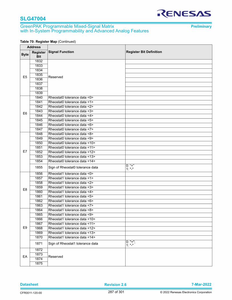
Datasheet 7-Mar-2022
CFR0011-120-00
Revision 2.6
287 of 301 © 2022 Renesas Electronics Corporation
SLG47004
GreenPAK Programmable Mixed-Signal Matrix with In-System Programmability and Advanced Analog Features
Preliminary
E5
1832
Reserved
1833183418351836183718381839
E6
1840 Rheostat0 tolerance data <0>1841 Rheostat0 tolerance data <1>1842 Rheostat0 tolerance data <2>1843 Rheostat0 tolerance data <3>1844 Rheostat0 tolerance data <4>1845 Rheostat0 tolerance data <5>1846 Rheostat0 tolerance data <6>1847 Rheostat0 tolerance data <7>
E7
1848 Rheostat0 tolerance data <8>1849 Rheostat0 tolerance data <9>1850 Rheostat0 tolerance data <10>1851 Rheostat0 tolerance data <11>1852 Rheostat0 tolerance data <12>1853 Rheostat0 tolerance data <13>1854 Rheostat0 tolerance data <14>
1855 Sign of Rheostat0 tolerance data 0: “+”1: "-"
E8
1856 Rheostat1 tolerance data <0>1857 Rheostat1 tolerance data <1>1858 Rheostat1 tolerance data <2>1859 Rheostat1 tolerance data <3>1860 Rheostat1 tolerance data <4>1861 Rheostat1 tolerance data <5>1862 Rheostat1 tolerance data <6>1863 Rheostat1 tolerance data <7>
E9
1864 Rheostat1 tolerance data <8>1865 Rheostat1 tolerance data <9>1866 Rheostat1 tolerance data <10>1867 Rheostat1 tolerance data <11>1868 Rheostat1 tolerance data <12>1869 Rheostat1 tolerance data <13>1870 Rheostat1 tolerance data <14>
1871 Sign of Rheostat1 tolerance data 0: "+"; 1: "-"
EA
1872
Reserved 187318741875
Table 70: Register Map (Continued)
Address
Signal Function Register Bit DefinitionByte
Register
Bit
Datasheet 7-Mar-2022
CFR0011-120-00
Revision 2.6
288 of 301 © 2022 Renesas Electronics Corporation
SLG47004
GreenPAK Programmable Mixed-Signal Matrix with In-System Programmability and Advanced Analog Features
Preliminary
EA
1876
Reserved187718781879
EB
1880
Reserved1881188218831884 Reserved
1885 Reserved
1886 Reserved 1887 Reserved
EC
1888 Reserved1889 Reserved1890 Reserved1891 Reserved1892 Reserved1893 Reserved1894 Reserved1895 Reserved
ED
1896 Reserved1897 Reserved1898 Reserved1899 Reserved1900 Reserved1901 Reserved1902 Reserved1903 Reserved
EE
1904 Reserved1905 Reserved1906 Reserved1907 Reserved1908 Reserved1909 Reserved 1910 Reserved 1911 Reserved
EF
1912 Reserved1913 Reserved1914 Reserved1915 Reserved1916 Reserved1917 Reserved 1918 Reserved 1919 Reserved
Table 70: Register Map (Continued)
Address
Signal Function Register Bit DefinitionByte
Register
Bit

Datasheet 7-Mar-2022
CFR0011-120-00
Revision 2.6
289 of 301 © 2022 Renesas Electronics Corporation
SLG47004
GreenPAK Programmable Mixed-Signal Matrix with In-System Programmability and Advanced Analog Features
Preliminary
F0
1920
Reserved
1921192219231924192519261927
F1
1928
Reserved
1929193019311932193319341935
F2
1936
Reserved
1937193819391940194119421943
F3
1944 Service page lock bit 0: Service page can be changed1: Service page is locked
1945 BG Chopper off 0: chopper enable1: chopper off
1946 Reserved 1947 Reserved
1948 BG register power down 0: power on1: power off
1949 Reserved1950 Reserved 1951 Reserved
F4
1952 Reserved1953 Reserved
1954 Reserved
1955 Reserved1956 Reserved1957 Reserved1958 Reserved1959 Reserved
Table 70: Register Map (Continued)
Address
Signal Function Register Bit DefinitionByte
Register
Bit

Datasheet 7-Mar-2022
CFR0011-120-00
Revision 2.6
290 of 301 © 2022 Renesas Electronics Corporation
SLG47004
GreenPAK Programmable Mixed-Signal Matrix with In-System Programmability and Advanced Analog Features
Preliminary
F5
1960 Reserved1961 Reserved1962 Reserved 1963 Reserved1964 Reserved1965 Reserved1966 Reserved1967 Reserved
F6
1968
I2C write mask bits 0: overwrite;1: mask the bit which set to high
1969197019711972197319741975
F7
1976
Reserved
1977197819791980198119821983
F8
1984
Reserved
1985198619871988198919901991
F9
1992
Reserved
1993199419951996199719981999 Reserved
Table 70: Register Map (Continued)
Address
Signal Function Register Bit DefinitionByte
Register
Bit
Datasheet 7-Mar-2022
CFR0011-120-00
Revision 2.6
291 of 301 © 2022 Renesas Electronics Corporation
SLG47004
GreenPAK Programmable Mixed-Signal Matrix with In-System Programmability and Advanced Analog Features
Preliminary
FA
2000
Reserved 2001200220032004
2005 Reserved
2006 Reserved
2007 Reserved
FB
2008
Reserved20092010201120122013 Reserved2014 Reserved2015 Reserved
FC
2016
Reserved20172018201920202021 Reserved2022 Reserved2023 Reserved
FD
2024
Reserved20252026202720282029 Reserved2030 Reserved2031 Reserved
FE
2032
Reserved20332034203520362037 Reserved 2038 Reserved 2039 Reserved
Table 70: Register Map (Continued)
Address
Signal Function Register Bit DefinitionByte
Register
Bit
Datasheet 7-Mar-2022
CFR0011-120-00
Revision 2.6
292 of 301 © 2022 Renesas Electronics Corporation
SLG47004
GreenPAK Programmable Mixed-Signal Matrix with In-System Programmability and Advanced Analog Features
Preliminary
FF
2040 Reserved2041 Reserved2042 Reserved2043 Reserved2044 Reserved2045 Reserved2046 Reserved2047 Reserved
Table 70: Register Map (Continued)
Address
Signal Function Register Bit DefinitionByte
Register
Bit
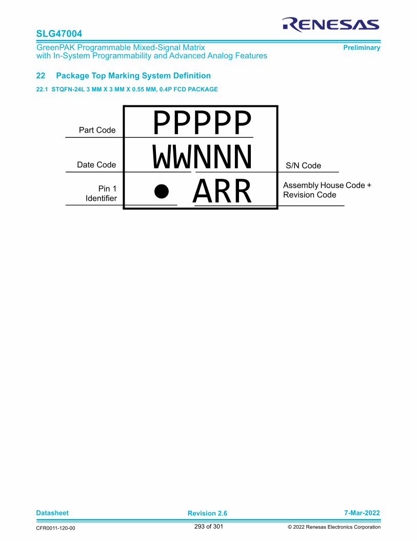
Datasheet 7-Mar-2022
CFR0011-120-00
Revision 2.6
293 of 301 © 2022 Renesas Electronics Corporation
SLG47004
GreenPAK Programmable Mixed-Signal Matrix with In-System Programmability and Advanced Analog Features
Preliminary
22 Package Top Marking System Definition
22.1 STQFN-24L 3 MM X 3 MM X 0.55 MM, 0.4P FCD PACKAGE
PPPPPPart Code
Pin 1Identifier
WWNNN S/N Code
ARR
Date Code
Assembly House Code + Revision Code

Datasheet 7-Mar-2022
CFR0011-120-00
Revision 2.6
294 of 301 © 2022 Renesas Electronics Corporation
SLG47004
GreenPAK Programmable Mixed-Signal Matrix with In-System Programmability and Advanced Analog Features
Preliminary
23 Package Information
23.1 PACKAGE OUTLINES FOR STQFN 24L 3 MM X 3 MM X 0.55 MM 0.4P GREEN PACKAGE
JEDEC MO-220
IC Net Weight: 0.0116 g
23.2 STQFN HANDLING
Be sure to handle STQFN package only in a clean, ESD-safe environment. Tweezers or vacuum pick-up tools are suitable forhandling. Do not handle STQFN package with fingers as this can contaminate the package pins and interface with solder reflow.
23.3 SOLDERING INFORMATION
Please see IPC/JEDEC J-STD-020: for relevant soldering information. More information can be found at www.jedec.org.
Bottom View
Side View
Top View

Datasheet 7-Mar-2022
CFR0011-120-00
Revision 2.6
295 of 301 © 2022 Renesas Electronics Corporation
SLG47004
GreenPAK Programmable Mixed-Signal Matrix with In-System Programmability and Advanced Analog Features
Preliminary
24 Ordering Information
24.1 TAPE AND REEL SPECIFICATIONS
24.2 CARRIER TAPE DRAWING AND DIMENSIONS
Note: Orientation in carrier: Pin1 is at upper left corner (Quadrant1).
Part Number Type
SLG47004V 24-pin STQFN
SLG47004VTR 24-pin STQFN - Tape and Reel (5k units)
Package
Type
# of
Pins
Nominal
Package Size
(mm)
Max Units Reel &
Hub Size
(mm)
Leader (min) Trailer (min) Tape
Width
(mm)
Part
Pitch
(mm)per Reel per Box PocketsLength
(mm)Pockets
Length
(mm)
STQFN 24L 3 mm x3 mm
0.4P FC Green
24 3 x 3 x 0.55 5.000 10.000 330 / 100 42 336 42 336 12 8
Package
Type
Pocket BTM
Length
(mm)
Pocket BTM
Width
(mm)
Depth
(mm)
Index Hole
Pitch
(mm)
Pitch
(mm)
Index Hole
Diameter
(mm)
Index Hole
to Tape
Edge
(mm)
Index Hole
to Pocket
Center
(mm)
Tape Width
(mm)
A0 B0 K0 P0 P1 D0 E F W
STQFN 24L 3 mm x3 mm
0.4P FC Green
3.3 3.3 0.8 4 8 1.55 1.75 5.5 12
Notes:1. 10 SPROCKET HOLE PITCH CUMULATIVE TOLERANCE ±0.22. POCKET POSITION RELATIVE TO SPROCKET HOLE MEASURED AS TRUE POSITION OF POCKET, NOT POCKET HOLE3. A0 AND B0 ARE CALCULATED ON A PLANE AT A DISTANCE “R” ABOVE THE BOTTOM OF THE POCKET.

Datasheet 7-Mar-2022
CFR0011-120-00
Revision 2.6
296 of 301 © 2022 Renesas Electronics Corporation
SLG47004
GreenPAK Programmable Mixed-Signal Matrix with In-System Programmability and Advanced Analog Features
Preliminary
25 Layout Guidelines
SLG47004 has two analog supply pins and two ground pins: VDD, VDDA, GND and AGND. Separating analog supply voltagefrom digital one helps to minimize noise generated by the digital part of IC.
Analog supply voltage domain: operational amplifiers, charge pumps for op amps, charge pumps for Oscillators, bias generatorsand regulators for op amps, digital rheostats, Chopper ACMP, HD Buffer, Vref of op amp and HD Buffer, Low Power Bandgap.
Digital supply voltage domain: ACMPs, Vref of ACMPs, Vref output buffers, Oscillator 0, Oscillator 1, Oscillator 2, I2C macrocell,NVM logic, Multi-function and Combination Function macrocells.
Analog and digital grounds must be connected together on the PCB board. The place of connection depends on usersschematic. For application cases with low digital current of SLG47004, both AGND and GND should be connected to analogground plane.
It is strongly recommended to connect I0 (Pin21) to the ground if it is not used in the project.
The following suggestions allow to minimize the impact of digital blocks operation on the analog macrocells: decrease the slew rate of input digital signals use proper grounding. If possible, use grounding polygons along the input/output digital traces to interface digital signals first use IO1, IO2, IO3, IO4, then use other GPIOs.
25.1 STQFN 24L 3 MM X 3 MM X 0.55 MM 0.4P GREEN PACKAGE

Datasheet 7-Mar-2022
CFR0011-120-00
Revision 2.6
297 of 301 © 2022 Renesas Electronics Corporation
SLG47004
GreenPAK Programmable Mixed-Signal Matrix with In-System Programmability and Advanced Analog Features
Preliminary
Glossary
A
ACK Acknowledge bit
ACMP Analog Comparator
ACMPH Analog Comparator High Speed
ACMPL Analog Comparator Low Power
AS Analog Switch
B
BG Bandgap
C
CLK Clock
CMO Connection matrix output
CNT Counter
D
DFF D Flip-Flop
DI Digital InputDILV Low Voltage Digital Input
DLY Delay
DNL Differential Non-Linearity
DR Digital Rheostat
E
EC Electrical Characteristics
ERSE Erase Enable
ERSR Erase Register
ESD Electrostatic discharge
EV End Value
F
FSM Finite State Machine
G
GPI General Purpose Input
GPIO General Purpose Input/Output
GPO General Purpose Output
I
IN Input
In Amp Instrumentation Amplifier

Datasheet 7-Mar-2022
CFR0011-120-00
Revision 2.6
298 of 301 © 2022 Renesas Electronics Corporation
SLG47004
GreenPAK Programmable Mixed-Signal Matrix with In-System Programmability and Advanced Analog Features
Preliminary
DNL Differential Non-Linearity
INL Integral Non-Linearity
IO Input/Output
L
LPF Low Pass Filter
LSB Least Significant Bit
LUT Look Up Table
LV Low Voltage
M
MSB Most Significant Bit
MTP Multiple-Time-Programmable
MUX Multiplexer
N
NPR Non-Volatile Memory Read/Write/Erase Protection
nRST Reset
NVM Non-Volatile Memory
O
OA Operational Amplifier
OD Open-Drain
OE Output Enable
Op Amp Operational Amplifier
OSC Oscillator
OUT Output
P
PD Power-down
PGen Pattern Generator
POR Power-On Reset
PP Push-Pull
PRL Protect Lock Bit
PT Programmable Trim
PWR Power
P DLY Programmable Delay
R
RPR Register Read/Write Protection
RPRB Register Read/Write Protection Bit

Datasheet 7-Mar-2022
CFR0011-120-00
Revision 2.6
299 of 301 © 2022 Renesas Electronics Corporation
SLG47004
GreenPAK Programmable Mixed-Signal Matrix with In-System Programmability and Advanced Analog Features
Preliminary
RPRL Register Protection Read/Write/Erase Lock
R/W Read/Write
S
SCL I2C Clock Input
SDA I2C Data Input/Output
SLA Slave Address
SMT With Schmitt Trigger
SPST Single-pole/Single throw
SV nSET Value
T
TS Temperature Sensor
V
Vref Voltage Reference
W
WOSMT Without Schmitt Trigger
WPB Write Protect Bit
WPR Write Protection Register
WPRE Write Protect Enable
WS Wake and Sleep Controller

Datasheet 7-Mar-2022
CFR0011-120-00
Revision 2.6
300 of 301 © 2022 Renesas Electronics Corporation
SLG47004
GreenPAK Programmable Mixed-Signal Matrix with In-System Programmability and Advanced Analog Features
Preliminary
Revision History
Revision Date Description
2.6 7-Mar-2021
Updated bytes 70, 71 in register mapRenesas rebrandingUpdated Pull-up or Pull-down Resistance Parameter in EC tableFixed typosAdded IC Net Weight in Package Information sectionUpdated registers [778], [779]
2.5 12-Oct-2021Updated all tables in Characteristics sectionUpdated Layout GuidelinesUpdated section External Clocking
2.4 10-Mar-2021 Updated Carrier Tape Drawing and DimensionsAdded Vref Performance: Typical Input Offset Voltage vs. Vref
2.3 2-Mar-2021
Updated Tape and Reel SpecificationAdded Op Amps, Analog Switches, Rheostats, OSCs, ACMPs, TS, Vref Typical PerformanceUpdated Thermal Resistance parameter in Absolute Maximum Ratings TableUpdated Op Amp Typical PerformanceUpdated 100K Digital Rheostat EC
2.2 3-Dec-2020Updated table Read/Write Register Protection OptionsUpdated Analog Switch Spec ConditionsFixed typos
2.1 13-Nov-2020 Removed TSSOP Package
2.0 9-Nov-2020 Preliminary version
Datasheet 7-Mar-2022
CFR0011-120-00
Revision 2.6
301 of 301 © 2022 Renesas Electronics Corporation
SLG47004
GreenPAK Programmable Mixed-Signal Matrix with In-System Programmability and Advanced Analog Features
Preliminary
Status Definitions
RoHS Compliance
Renesas Electronics Corporation's suppliers certify that its products are in compliance with the requirements of Directive 2011/65/EU of the European Parliament on therestriction of the use of certain hazardous substances in electrical and electronic equipment. RoHS certificates from our suppliers are available on request.
Revision Datasheet Status Product Status Definition
1.<n> Target Development This datasheet contains the design specifications for product development. Specifications may change in any manner without notice.
2.<n> Preliminary Qualification This datasheet contains the specifications and preliminary characterization data for products in pre-production. Specifications may be changed at any time without notice in order to improve the design.
3.<n> Final Production This datasheet contains the final specifications for products in volume production. The specifications may be changed at any time in order to improve the design, manufacturing and supply. Major specification changes are communicated via Customer Product Notifications. Datasheet changes are communicated via www.renesas.com.
4.<n> Obsolete Archived This datasheet contains the specifications for discontinued products. The information is provided for reference only.

Corporate HeadquartersTOYOSU FORESIA, 3-2-24 Toyosu,Koto-ku, Tokyo 135-0061, Japanwww.renesas.com
Contact InformationFor further information on a product, technology, the most up-to-date version of a document, or your nearest sales office, please visit:www.renesas.com/contact/
TrademarksRenesas and the Renesas logo are trademarks of Renesas Electronics Corporation. All trademarks and registered trademarks are the property of their respective owners.
IMPORTANT NOTICE AND DISCLAIMER
RENESAS ELECTRONICS CORPORATION AND ITS SUBSIDIARIES (“RENESAS”) PROVIDES TECHNICAL SPECIFICATIONS AND RELIABILITY DATA (INCLUDING DATASHEETS), DESIGN RESOURCES (INCLUDING REFERENCE DESIGNS), APPLICATION OR OTHER DESIGN ADVICE, WEB TOOLS, SAFETY INFORMATION, AND OTHER RESOURCES “AS IS” AND WITH ALL FAULTS, AND DISCLAIMS ALL WARRANTIES, EXPRESS OR IMPLIED, INCLUDING, WITHOUT LIMITATION, ANY IMPLIED WARRANTIES OF MERCHANTABILITY, FITNESS FOR A PARTICULAR PURPOSE, OR NON-INFRINGEMENT OF THIRD PARTY INTELLECTUAL PROPERTY RIGHTS.
These resources are intended for developers skilled in the art designing with Renesas products. You are solely responsible for (1) selecting the appropriate products for your application, (2) designing, validating, and testing your application, and (3) ensuring your application meets applicable standards, and any other safety, security, or other requirements. These resources are subject to change without notice. Renesas grants you permission to use these resources only for development of an application that uses Renesas products. Other reproduction or use of these resources is strictly prohibited. No license is granted to any other Renesas intellectual property or to any third party intellectual property. Renesas disclaims responsibility for, and you will fully indemnify Renesas and its representatives against, any claims, damages, costs, losses, or liabilities arising out of your use of these resources. Renesas' products are provided only subject to Renesas' Terms and Conditions of Sale or other applicable terms agreed to in writing. No use of any Renesas resources expands or otherwise alters any applicable warranties or warranty disclaimers for these products.
(Rev.1.0 Mar 2020)
© 2021 Renesas Electronics Corporation. All rights reserved.