FN9141 Rev.8.00 Page 1 of 10 Aug 8, 2019 FN9141 Rev.8.00 Aug 8, 2019 ISL6506A, ISL6506B Multiple Linear Power Controller with ACPI Control Interface DATASHEET The ISL6506A and ISL6506B complement other power building blocks (voltage regulators) in ACPI-compliant designs for microprocessor and computer applications. They integrate the control of the 5V DUAL and 3.3V DUAL rails into an 8 Ld EPAD SOIC package. The ISL6506A and ISL6506B’s operating mode (active outputs or sleep outputs) is selectable through two digital control pins; S3 and S5 . A completely integrated linear regulator generates the 3.3V DUAL voltage plane from the ATX supply’s 5V SB output during sleep states (S3, S4/S5). In active states (during S0 and S1/S2), the ISL6506A and ISL6506B use an external N-Channel pass MOSFET to connect the outputs directly to the 3.3V input supplied by an ATX power supply, for minimal losses. The ISL6506A and ISL6506B power up the 5V DUAL plane by switching in the ATX 5V output through an NMOS transistor in active states, or by switching in the ATX 5V SB through a PMOS (or PNP) transistor in S3 sleep state. In S4/S5 sleep states, the ISL6506B 5V DUAL output is shut down. In the ISL6506A, the 5V DUAL output stays on during S4/S5 sleep states. The ISL6506A and ISL6506B are functionally identical, except for the sleep mode in the preceding paragraph. In addition, the ISL6506A has a 1A current limit on the internal 3.3V LDO; the ISL6506B has a 2A current limit. Related Literature For a full list of related documents, visit our website: • ISL6506A , ISL6506B Features • Provides 2 ACPI-Controlled Voltages - 5V DUAL USB/Keyboard/Mouse - 3.3V DUAL /3.3V SB PCI/Auxiliary/LAN • Excellent 3.3V DUAL Regulation in S3/S4/S5 - ±2.0% Over-Temperature - 1A Capability on ISL6506A - 2A Capability on ISL6506B • Small Size; Very Low External Component Count • Over-Temperature Shutdown • Pb-Free Available (RoHS Compliant) Applications • ACPI-Compliant Power Regulation for Motherboards - ISL6506B: 5V DUAL is shut down in S4/S5 sleep states - ISL6506A: 5V DUAL stays on in S4/S5 sleep states Pinout 8 LD EPSOIC TOP VIEW VCC 3V3AUX S3 S5 1 2 3 4 8 7 6 5 N/C 5VDLSB DLA GND GND Ordering Information PART NUMBER (Notes 2 , 3 ) PART MARKING TEMP. RANGE (°C) TAPE AND REEL (Units) (Note 1 ) PACKAGE (RoHS Compliant) PKG. DWG. # ISL6506ACBZ 6506 ACBZ 0 to +70 - 8 Ld EPSOIC M8.15C ISL6506ACBZ-T 6506 ACBZ 0 to +70 2.5k 8 Ld EPSOIC M8.15C ISL6506BCBZ 6506 BCBZ 0 to +70 - 8 Ld EPSOIC M8.15C ISL6506BCBZ-T 6506 BCBZ 0 to +70 2.5k 8 Ld EPSOIC M8.15C ISL6506BCBZA 6506 BCBZ 0 to +70 - 8 Ld EPSOIC M8.15C ISL6506BCBZA-T 6506 BCBZ 0 to +70 2.5k 8 Ld EPSOIC M8.15C NOTES: 1. See TB347 for details about reel specifications. 2. These Pb-free plastic packaged products employ special Pb-free material sets, molding compounds/die attach materials, and 100% matte tin plate plus anneal (e3 termination finish, which is RoHS compliant and compatible with both SnPb and Pb-free soldering operations). Pb-free products are MSL classified at Pb-free peak reflow temperatures that meet or exceed the Pb-free requirements of IPC/JEDEC J-STD-020. 3. For Moisture Sensitivity Level (MSL), see the ISL6506A , ISL6506B device pages. For more information about MSL, see TB363 .

Welcome message from author
This document is posted to help you gain knowledge. Please leave a comment to let me know what you think about it! Share it to your friends and learn new things together.
Transcript
FN9141Rev.8.00
Aug 8, 2019
ISL6506A, ISL6506BMultiple Linear Power Controller with ACPI Control Interface
DATASHEET
The ISL6506A and ISL6506B complement other power building blocks (voltage regulators) in ACPI-compliant designs for microprocessor and computer applications. They integrate the control of the 5VDUAL and 3.3VDUAL rails into an 8 Ld EPAD SOIC package. The ISL6506A and ISL6506B’s operating mode (active outputs or sleep outputs) is selectable through two digital control pins; S3 and S5.
A completely integrated linear regulator generates the 3.3VDUAL voltage plane from the ATX supply’s 5VSB output during sleep states (S3, S4/S5). In active states (during S0 and S1/S2), the ISL6506A and ISL6506B use an external N-Channel pass MOSFET to connect the outputs directly to the 3.3V input supplied by an ATX power supply, for minimal losses.
The ISL6506A and ISL6506B power up the 5VDUAL plane by switching in the ATX 5V output through an NMOS transistor in active states, or by switching in the ATX 5VSB through a PMOS (or PNP) transistor in S3 sleep state. In S4/S5 sleep states, the ISL6506B 5VDUAL output is shut down. In the ISL6506A, the 5VDUAL output stays on during S4/S5 sleep states.
The ISL6506A and ISL6506B are functionally identical, except for the sleep mode in the preceding paragraph. In addition, the ISL6506A has a 1A current limit on the internal 3.3V LDO; the ISL6506B has a 2A current limit.
Related Literature
For a full list of related documents, visit our website:
• ISL6506A, ISL6506B
Features
• Provides 2 ACPI-Controlled Voltages
- 5VDUAL USB/Keyboard/Mouse
- 3.3VDUAL/3.3VSB PCI/Auxiliary/LAN
• Excellent 3.3VDUAL Regulation in S3/S4/S5
- ±2.0% Over-Temperature
- 1A Capability on ISL6506A
- 2A Capability on ISL6506B
• Small Size; Very Low External Component Count
• Over-Temperature Shutdown
• Pb-Free Available (RoHS Compliant)
Applications
• ACPI-Compliant Power Regulation for Motherboards- ISL6506B: 5VDUAL is shut down in S4/S5 sleep states
- ISL6506A: 5VDUAL stays on in S4/S5 sleep states
Pinout8 LD EPSOIC
TOP VIEW
VCC
3V3AUX
S3
S5
1
2
3
4
8
7
6
5
N/C
5VDLSB
DLA
GND
GND
Ordering Information
PART NUMBER (Notes 2, 3)
PART MARKING
TEMP. RANGE(°C)
TAPE AND REEL(Units) (Note 1)
PACKAGE(RoHS Compliant)
PKG. DWG. #
ISL6506ACBZ 6506 ACBZ 0 to +70 - 8 Ld EPSOIC M8.15C
ISL6506ACBZ-T 6506 ACBZ 0 to +70 2.5k 8 Ld EPSOIC M8.15C
ISL6506BCBZ 6506 BCBZ 0 to +70 - 8 Ld EPSOIC M8.15C
ISL6506BCBZ-T 6506 BCBZ 0 to +70 2.5k 8 Ld EPSOIC M8.15C
ISL6506BCBZA 6506 BCBZ 0 to +70 - 8 Ld EPSOIC M8.15C
ISL6506BCBZA-T 6506 BCBZ 0 to +70 2.5k 8 Ld EPSOIC M8.15C
NOTES:
1. See TB347 for details about reel specifications.
2. These Pb-free plastic packaged products employ special Pb-free material sets, molding compounds/die attach materials, and 100% matte tin plate plus anneal (e3 termination finish, which is RoHS compliant and compatible with both SnPb and Pb-free soldering operations). Pb-free products are MSL classified at Pb-free peak reflow temperatures that meet or exceed the Pb-free requirements of IPC/JEDEC J-STD-020.
3. For Moisture Sensitivity Level (MSL), see the ISL6506A, ISL6506B device pages. For more information about MSL, see TB363.
FN9141 Rev.8.00 Page 1 of 10Aug 8, 2019
ISL6506A, ISL6506B
Block Diagram
Typical Application
VCC S3 S5
5VDLSB
GND
UV DETECTOR
MONITORAND
CONTROL
+-
3V3AUX
VCC
DLA
TEMPERATUREMONITOR
DIGITALSOFT-START( )
EA1
7.5µA
SOFT-START
10µA 10µA12V PORSENSE3.5
SLP_S5
SLP_S3
VCC
3V3AUX
S3
S5
NC
5VDLSB
DLA
GND
ISL6506A/B
5VSBY 12VATX 5VSBY 5VATX3V3ATX
5VDUAL1
2
3
4
8
7
6
5
EP
AD
93V3DUAL
1k
Q1
Q2Q3
Cg(OPTIONAL)
FN9141 Rev.8.00 Page 2 of 10Aug 8, 2019
ISL6506A, ISL6506B
Absolute Maximum Ratings Thermal InformationSupply Voltage, V5VSB . . . . . . . . . . . . . . . . . . . . . . . . . . . . . . +7.0VDLA . . . . . . . . . . . . . . . . . . . . . . . . . . . . . . . . GND - 0.3V to +14.5VAll Other Pins . . . . . . . . . . . . . . . . . . . . . . . . . . . . . . . . . . . . . . +7.0VESD Rating
Human Body Model . . . . . . . . . . . . . . . . . . . . . . . . . . . . . . .4000V
Recommended Operating ConditionsSupply Voltage, V5VSB . . . . . . . . . . . . . . . . . . . . . . . . . . . +5V ±5%Lowest 5VSB Supply Voltage Guaranteeing Parameters . . . . +4.5VDigital Inputs, VSx . . . . . . . . . . . . . . . . . . . . . . . . . . . . . 0V to +5.5VAmbient Temperature Range. . . . . . . . . . . . . . . . . . . . 0°C to +70°CJunction Temperature Range. . . . . . . . . . . . . . . . . . . 0°C to +125°C
Thermal Resistance (Typical) JA (°C/W) JC (°C/W)
EPSOIC Package (Notes 4, 5) . . . . . . 40 3.5Maximum Junction Temperature (Plastic Package) . . . . . . . +150°CMaximum Storage Temperature Range . . . . . . . . . .-65°C to +150°CPb-Free Reflow Profile. . . . . . . . . . . . . . . . . . . . . . . . . . . see TB493
CAUTION: Do not operate at or near the maximum ratings listed for extended periods of time. Exposure to such conditions can adversely impact product reliability andresult in failures not covered by warranty.
NOTES:
4. JA is measured in free air with the component mounted on a high-effective thermal conductivity test board with “direct attach” features.
5. For JC, the “case temp” location is the center of the exposed metal pad on the package underside.
Electrical Specifications Recommended Operating Conditions. Boldface limits apply over the operating temperature range, 0°C to +70°C.
PARAMETER SYMBOL TEST CONDITIONSMIN
(Note 6) TYPMAX
(Note 6) UNIT
VCC SUPPLY CURRENT
Nominal Supply Current I5VSB VS3 = 5V, VS5 = 5V (S0 State) - 3.60 - mA
VS3 = 0V, VS5 = 5V (S3 State) - 4.60 - mA
VS5 = 0V (S5 State) - 4.60 - mA
POWER-ON RESET
Rising 5VSB POR Threshold - - 4.5 V
Falling 5VSB POR Threshold 3.60 - 3.95 V
Rising 12V POR Threshold 1.00kΩ resistor between DLA and 12V Rail 8.9 9.8 10.8 V
3.3VAUX LINEAR REGULATOR
Regulation V5VSBY = 5.0V, I3V3SB = 0A - - 2.0 %
3V3SB Nominal Voltage Level V3V3SB - 3.3 - V
3V3SB Undervoltage Threshold V3V3SB_UV - 2.475 - V
3V3SB Overcurrent Trip I3V3SB_TRIP ISL6506A - - 1 A
ISL6506B - - 2 A
5VDUAL SWITCH CONTROLLER
5VDLSB Output Drive Current I5VDLSB V5VDLSB = 4V, V5VSB = 5V 20 - 35 mA
TIMING INTERVAL
S0 to S3 Transition Delay - 58 - µs
SOFT-START
Soft-start Interval tSS 6.55 8.2 9.85 ms
5VDLSB Soft-start Current Source - -7.5 - µA
CONTROL I/O (S3, S5)
High Level Input Threshold - - 2.2 V
Low Level Input Threshold 0.8 - - V
S3, S5 Internal Pull-down Current to GND - 10 - µA
TEMPERATURE MONITOR
Shutdown-Level Threshold - 140 - °C
NOTE:
6. Compliance to datasheet limits is assured by one or more methods: production test, characterization, and/or design.
FN9141 Rev.8.00 Page 3 of 10Aug 8, 2019
ISL6506A, ISL6506B
Functional Pin Description
VCC (Pin 1)
Provide a very well decoupled 5V bias supply for the IC to this pin by connecting it to the ATX 5VSB output. This pin provides all the bias for the IC as well as the input voltage for the internal standby 3V3AUX LDO. The voltage at this pin is monitored for power-on reset (POR) purposes.
GND (Pin 5, Pad)
Signal ground for the IC. These pins are also the ground return for the internal 3V3AUX LDO that is active in S3/S4/S5 sleep states. All voltage levels are measured with respect to these pins.
S3 and S5 (Pins 3 and 4)
These pins switch the IC’s operating state from active (S0, S1/S2) to S3 and S4/S5 sleep states. These are digital inputs featuring internal 10µA pull-down current sources on each pin. Additional circuitry blocks illegal state transitions, such as S4/S5 to S3. Connect S3 and S5 to the computer system’s SLP_S3 and SLP_S5 signals, respectively.
3V3AUX (Pin 2)
Connect this pin to the 3V3DUAL output. In sleep states, the voltage at this pin is regulated to 3.3V through an internal pass device powered from 5VSBY through the VCC pin. In active states, ATX 3.3V output is delivered to this node through a fully-on NMOS transistor. During S3 and S4/S5 states, this pin is monitored for undervoltage events.
DLA (Pin 6)
This pin is an open-drain output. A 1kΩ resistor must be connected from this pin to the ATX 12V output. This resistor is used to pull the gates of suitable N-MOSFETs to 12V, which in active state, switch in the ATX 3.3V and 5V outputs into the 3.3VAUX and 5VDUAL outputs, respectively. This pin is also used to monitor the 12V rail during POR. If a resistor other than 1kΩ is used, the POR level will be affected.
5VDLSB (Pin 7)
Connect this pin to the gate of a suitable P-MOSFET.
ISL6506B: In S3 sleep state, this transistor is switched on, connecting the ATX 5VSB output to the 5VDUAL regulator output.
ISL6506A: In S3 and S4/S5 sleep state, this transistor is switched on, connecting the ATX 5VSB output to the 5VDUAL regulator output.
Description
Operation
The ISL6506A and ISL6506B control two output voltages, 3.3VDUAL and 5VDUAL. They are designed for microprocessor computer applications requiring 3.3V, 5V, 5VSB, and 12V bias input from an ATX power supply. The
ICs are composed of one linear controller/regulator supplying the computer system’s 3.3VDUAL power, a dual switch controller supplying the 5VDUAL voltage, and all the control and monitoring functions necessary for complete ACPI implementation.
Initialization
The ISL6506A and ISL6506B automatically initialize on receipt of input power. The Power-On Reset (POR) function continually monitors the 5VSB input supply voltage. The ISL6506A and ISL6506B also monitor the 12V rail to ensure that the ATX rails are up before entering into the S0 state even if both SLP_S3 and SLP_S5 are both high.
Dual Outputs Operational Truth Table
Table 1 describes the truth combinations pertaining to the 3.3VDUAL and 5VDUAL outputs. The internal circuitry does not allow the transition from an S4/S5 state to an S3 state.
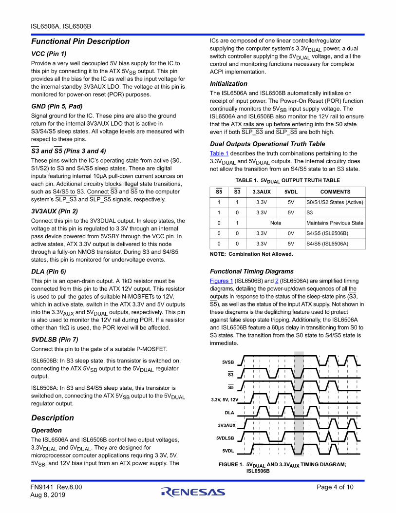
Functional Timing Diagrams
Figures 1 (ISL6506B) and 2 (ISL6506A) are simplified timing diagrams, detailing the power-up/down sequences of all the outputs in response to the status of the sleep-state pins (S3, S5), as well as the status of the input ATX supply. Not shown in these diagrams is the deglitching feature used to protect against false sleep state tripping. Additionally, the ISL6506A and ISL6506B feature a 60µs delay in transitioning from S0 to S3 states. The transition from the S0 state to S4/S5 state is immediate.
TABLE 1. 5VDUAL OUTPUT TRUTH TABLE
S5 S3 3.3AUX 5VDL COMMENTS
1 1 3.3V 5V S0/S1/S2 States (Active)
1 0 3.3V 5V S3
0 1 Note Maintains Previous State
0 0 3.3V 0V S4/S5 (ISL6506B)
0 0 3.3V 5V S4/S5 (ISL6506A)
NOTE: Combination Not Allowed.
FIGURE 1. 5VDUAL AND 3.3VAUX TIMING DIAGRAM; ISL6506B
5VSB
3.3V, 5V, 12V
S3
S5
5VDLSB
DLA
3V3AUX
5VDL
FN9141 Rev.8.00 Page 4 of 10Aug 8, 2019
ISL6506A, ISL6506B
Soft-Start
Figures 3 and 4 show the soft-start sequence for the typical application start-up into a sleep state. At time t0, 5VSB (bias) is applied to the circuit. At time t1, the 5VSB surpasses POR level. Time t2, one soft-start interval after t1, denotes the initiation of soft-start. The 3.3VDUAL rail is brought up through the internal standby LDO through an internal digital soft-start function. Figure 4 shows the 5VDUAL rail initiating a soft-start at time t2 as well. The ISL6506A draws 7.5µA into the 5VDLSB for a duration of one soft-start period. This current will enhance the P-MOSFET (Q2, see “Typical Application” on page 2) in a controlled manner. At time t3, the 3.3VDUAL is in regulation and the 5VDLSB pin is pulled down to ground. If the 5VDUAL rail has not reached the level of the 5VSB rail by time t3, then the rail will experience a sudden step as the P-MOSFET gate is fully enhanced. The soft-start profile of the 5VDUAL may be altered by placing a capacitor between the gate and drain of the P-MOSFET. Adding this capacitor will increase the gate capacitance and slow down the start of the 5VDUAL rail.
At time t4, the system has transitioned into S0 state and the ATX supplies have begun to ramp-up. With the ISL6506B (Figure 3), the 5VDUAL rail will begin to ramp-up from the 5VATX rail through the body diode of the N-MOSFET (Q3). The ISL6506A already has the 5VDUAL rail in regulation (Figure 4). At time t5, the 12VATX rail has surpassed the 12V POR level. Time t6 is three soft-start cycles after the 12V POR level has been surpassed. At time t6, three events occur simultaneously. The DLA pin is forced to a high impedance state, which allows the 12V rail to enhance the two N-MOSFETs (Q1 and Q3) that connect the ATX rails to the 3.3VDUAL and 5VDUAL rails. The 5VDLSB pin is actively pulled high, which turns the P-MOSFET (Q2) off. Finally, the internal LDO that regulates the 3.3VAUX rail in sleep states is put in standby mode.
Sleep to Wake State Transitions
Figures 3 and 4, starting at time t4, depict the transitions from sleep states to the S0 wake state. Figure 3 shows the transition of the ISL6506B from the S4/S5 state to the S0 state. Figure 4 shows how the ISL6506B transitions from the S3 sleep state into S0 state. Figure 3 also shows how the ISL6506A transitions from either S3 or S4/S5 in the S0 state. For all transitions, t4 depicts the system transition into the S0 state. Here, the ATX supplies are enabled and begin to ramp up. At time t5, the 12VATX rail has exceeded the POR threshold for the ISL6506B and ISL6506A. Three soft-start periods after time t5, at time t6, three events occur simultaneously. The DLA pin is forced to a high impedance
FIGURE 2. 5VDUAL AND 3.3VAUX TIMING DIAGRAM; ISL6506A
5VSB
3.3V, 5V, 12V
S3
S5
5VDLSB
DLA
3V3DL
5VDL
0V
TIME
5VSB
(1V/DIV)
FIGURE 3. ISL6506B SOFT-START INTERVAL IN S4/S5 STATE AND S5 TO S0 TRANSITION
5VDUAL
(1V/DIV)
3.3VDUAL
(2V/DIV)
t1 t2 t3t0 t5t4 t6
DLA
(10V/DIV)
12VATX (2V/DIV)5VATX (1V/DIV)3.3VATX (1V/DIV)
FIGURE 4. SOFT-START INTERVAL FOR ISL6506A IN S4/S5 AND S5 TO S0 TRANSITION FOR ISL6506A. ALSO S3 TO S0 TRANSITION FOR ISL6506A, ISL6506B
0V
TIMEt1 t2 t3t0 t5t4 t6
5VDLSB
(5V/DIV)
5VSB
(1V/DIV)
5VDUAL
(1V/DIV)
3.3VDUAL
(2V/DIV)
DLA
(10V/DIV)
12VATX (2V/DIV)5VATX (1V/DIV)3.3VATX (1V/DIV)
FN9141 Rev.8.00 Page 5 of 10Aug 8, 2019
ISL6506A, ISL6506B
state, which allows the 12V rail to enhance the two N-MOSFETs (Q1 and Q3) that connect the ATX rails to the 3.3VDUAL and 5VDUAL rails. The 5VDLSB pin is actively pulled high, which turns the P-MOSFET (Q2) off. Finally, the internal LDO that regulates the 3.3VDUAL rail in sleep states is put in standby mode.
Internal Linear Regulator Undervoltage Protection
The undervoltage protection on the internal linear regulator is only active during sleep states and after the initial soft-start ramp of the 3.3V linear regulator. The undervoltage trip point is set at 25% below nominal, or 2.475V.
When an undervoltage is detected, the 3.3V linear regulator is disabled. One soft-start interval later, the 3.3V linear regulator is retried with a soft-start ramp. If the linear regulator is retried 3 times and a fourth undervoltage is detected, the 3.3V linear regulator is disabled and can only be reset through a POR reset.
Internal Linear Regulator Overcurrent Protection
When an overcurrent condition is detected, the gate voltage to the internal NMOS pass element is reduced, which causes the output voltage of the linear regulator to be reduced. When the output voltage is reduced to the undervoltage trip point, the undervoltage protection is initiated and the output will shutdown.
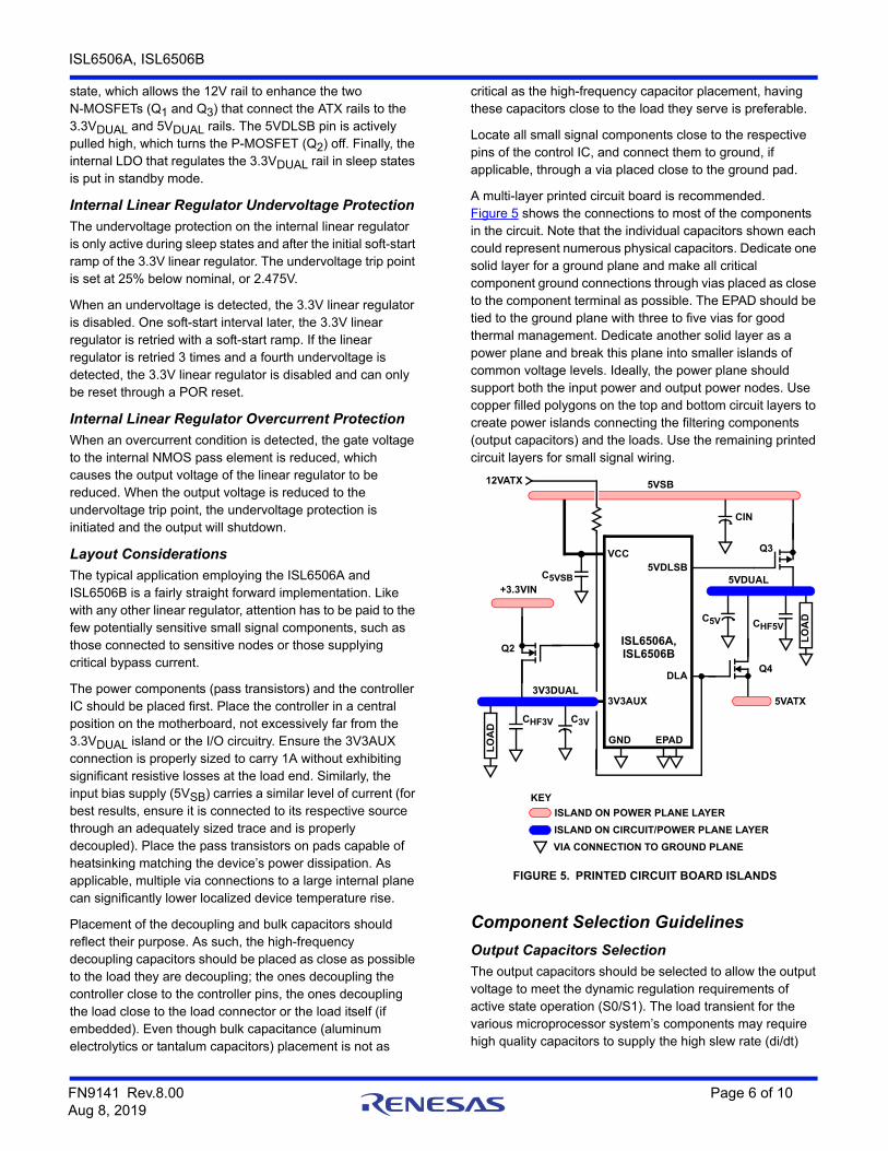
Layout Considerations
The typical application employing the ISL6506A and ISL6506B is a fairly straight forward implementation. Like with any other linear regulator, attention has to be paid to the few potentially sensitive small signal components, such as those connected to sensitive nodes or those supplying critical bypass current.
The power components (pass transistors) and the controller IC should be placed first. Place the controller in a central position on the motherboard, not excessively far from the 3.3VDUAL island or the I/O circuitry. Ensure the 3V3AUX connection is properly sized to carry 1A without exhibiting significant resistive losses at the load end. Similarly, the input bias supply (5VSB) carries a similar level of current (for best results, ensure it is connected to its respective source through an adequately sized trace and is properly decoupled). Place the pass transistors on pads capable of heatsinking matching the device’s power dissipation. As applicable, multiple via connections to a large internal plane can significantly lower localized device temperature rise.
Placement of the decoupling and bulk capacitors should reflect their purpose. As such, the high-frequency decoupling capacitors should be placed as close as possible to the load they are decoupling; the ones decoupling the controller close to the controller pins, the ones decoupling the load close to the load connector or the load itself (if embedded). Even though bulk capacitance (aluminum electrolytics or tantalum capacitors) placement is not as
critical as the high-frequency capacitor placement, having these capacitors close to the load they serve is preferable.
Locate all small signal components close to the respective pins of the control IC, and connect them to ground, if applicable, through a via placed close to the ground pad.
A multi-layer printed circuit board is recommended. Figure 5 shows the connections to most of the components in the circuit. Note that the individual capacitors shown each could represent numerous physical capacitors. Dedicate one solid layer for a ground plane and make all critical component ground connections through vias placed as close to the component terminal as possible. The EPAD should be tied to the ground plane with three to five vias for good thermal management. Dedicate another solid layer as a power plane and break this plane into smaller islands of common voltage levels. Ideally, the power plane should support both the input power and output power nodes. Use copper filled polygons on the top and bottom circuit layers to create power islands connecting the filtering components (output capacitors) and the loads. Use the remaining printed circuit layers for small signal wiring.
Component Selection Guidelines
Output Capacitors Selection
The output capacitors should be selected to allow the output voltage to meet the dynamic regulation requirements of active state operation (S0/S1). The load transient for the various microprocessor system’s components may require high quality capacitors to supply the high slew rate (di/dt)
FIGURE 5. PRINTED CIRCUIT BOARD ISLANDS
Q2
Q3
12VATX
CIN
VIA CONNECTION TO GROUND PLANE
ISLAND ON POWER PLANE LAYER
ISLAND ON CIRCUIT/POWER PLANE LAYER
GND
5VDLSB
KEY
VCC
5VSB
DLAQ4
C5V
LO
AD
C5VSB
LO
AD
CHF3V
CHF5V
5VATX
+3.3VIN
3V3AUX
C3V
5VDUAL
3V3DUAL
EPAD
ISL6506A,ISL6506B
FN9141 Rev.8.00 Page 6 of 10Aug 8, 2019
ISL6506A, ISL6506B
current demands. Thus, it is recommended that the output capacitors be selected for transient load regulation, paying attention to their parasitic components (ESR, ESL).
Also, during the transition between active and sleep states on the 5VDUAL output, there is a short interval of time during which none of the power pass elements are conducting. During this time the output capacitors have to supply all the output current. The output voltage drop during this brief period of time can be easily approximated using Equation 1:
where:
• VOUT = output voltage drop
• ESROUT = output capacitor bank ESR
• IOUT = output current during transition
• COUT = output capacitor bank capacitance
• tt = active-to-sleep/sleep-to-active transition time (10µs typical)
The output voltage drop is heavily dependent on the ESR (equivalent series resistance) of the output capacitor bank, the choice of capacitors should be such as to maintain the output voltage above the lowest allowable regulation level.
Input Capacitors Selection
The input capacitors for an ISL6506A and ISL6506B application must have a sufficiently low ESR so as not to allow the input voltage to dip excessively when energy is transferred to the output capacitors. If the ATX supply does not meet the specifications, certain imbalances between the ATX’s outputs and the ISL6506, ISL6506A’s regulation levels could have as a result a brisk transfer of energy from the input capacitors to the supplied outputs. At the transition between active and sleep states, such phenomena could be responsible for the 5VSB voltage drooping excessively and affecting the output regulation. The solution to such a potential problem is using larger input capacitors with a lower total combined ESR.
Transistor Selection/Considerations
The ISL6506A and ISL6506B usually require one P-Channel and two N-Channel MOSFETs. All three of these MOSFETs are used as ON/OFF switching elements.
One important criteria for selection of transistors for all the switching elements is package selection for efficient removal of heat. The power dissipated in a switch element while on is shown in Equation 2:
Select a package and heatsink that maintains the junction temperature below the rating with the maximum expected ambient temperature.
Q1, Q3
These N-Channel MOSFETs are used to switch the 3.3V and 5V inputs provided by the ATX supply into the 3.3VAUX and 5VDUAL outputs while in active (S0, S1) state. The main criteria for the selection of these transistors is output voltage budgeting. The maximum rDS(ON) allowed at highest junction temperature can be expressed using Equation 3:
where:
• VINmin = minimum input voltage
• VOUTmin = minimum output voltage allowed
• IOUTmax = maximum output current
Q2
This is a P-Channel MOSFET used to switch the 5VSB output of the ATX supply into the 5VDUAL output during sleep states. The selection criteria of this device, as with the N-Channel MOSFETs, is proper voltage budgeting. The maximum rDS(ON), however, has to be achieved with only 4.5V of gate-to-source voltage, so a true logic level MOSFET needs to be selected.
VOUT IOUT ESROUT
ttCOUT----------------+
= (EQ. 1)
PLOSS Io2
rDS ON = (EQ. 2)
rDS ON max
VINmin VOUTmin–
IOUTmax---------------------------------------------------= (EQ. 3)
FN9141 Rev.8.00 Page 7 of 10Aug 8, 2019
ISL6506A, ISL6506B
Revision HistoryThe revision history provided is for informational purposes only and is believed to be accurate, but not warranted. Please go to the web to make sure that you have the latest revision.
DATE REVISION CHANGE
Aug 8, 2019 8.00 Updated links throughout document.Added Related LiteratureRemoved ISL6506 information from document.Added tape and reel information to Ordering Information table and updated notes.Removed About Intersil sectionUpdated M8.15C POD to the latest version, changes are as follows:-Updated Millimeter MIN and MAX values for A from: 1.43 MIN and 1.68 MAX to: 1.422 MIN and 1.700 MAX-Updated Inch MAX for A from: 0.066 to: 0.067-A1 Inches changed MIN from: 0.001 to 0.0, and A1 Millimeters MIN from 0.03 to 0.0-L Millimeter Min changed from: 0.41 to 0.406
Nov 10, 2015 7.00 Updated the Ordering Information Table on page 1.Added Revision History.Added the About Intersil section.
FN9141 Rev.8.00 Page 8 of 10Aug 8, 2019
ISL6506A, ISL6506B
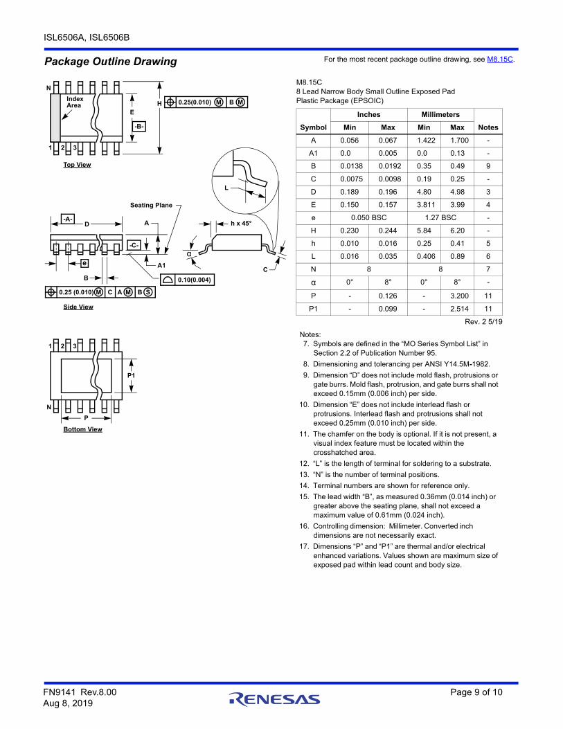
Package Outline Drawing
IndexArea
E
D
N
1 2 3
-B-
0.25 (0.010) C AM B S
e
-A-
L
B
M
-C-
A1
A
Seating Plane
0.10(0.004)
h x 45°
C
H 0.25(0.010) BM M
P1
1 2 3
P
Bottom View
N
Top View
Side View
M8.15C8 Lead Narrow Body Small Outline Exposed Pad Plastic Package (EPSOIC)
Symbol
Inches Millimeters
NotesMin Max Min Max
A 0.056 0.067 1.422 1.700 -
A1 0.0 0.005 0.0 0.13 -
B 0.0138 0.0192 0.35 0.49 9
C 0.0075 0.0098 0.19 0.25 -
D 0.189 0.196 4.80 4.98 3
E 0.150 0.157 3.811 3.99 4
e 0.050 BSC 1.27 BSC -
H 0.230 0.244 5.84 6.20 -
h 0.010 0.016 0.25 0.41 5
L 0.016 0.035 0.406 0.89 6
N 8 8 7
α 0° 8° 0° 8° -
P - 0.126 - 3.200 11
P1 - 0.099 - 2.514 11
Rev. 2 5/19
Notes:7. Symbols are defined in the “MO Series Symbol List” in
Section 2.2 of Publication Number 95.
8. Dimensioning and tolerancing per ANSI Y14.5M-1982.
9. Dimension “D” does not include mold flash, protrusions or gate burrs. Mold flash, protrusion, and gate burrs shall not exceed 0.15mm (0.006 inch) per side.
10. Dimension “E” does not include interlead flash or protrusions. Interlead flash and protrusions shall not exceed 0.25mm (0.010 inch) per side.
11. The chamfer on the body is optional. If it is not present, a visual index feature must be located within the crosshatched area.
12. “L” is the length of terminal for soldering to a substrate.
13. “N” is the number of terminal positions.
14. Terminal numbers are shown for reference only.
15. The lead width “B”, as measured 0.36mm (0.014 inch) or greater above the seating plane, shall not exceed a maximum value of 0.61mm (0.024 inch).
16. Controlling dimension: Millimeter. Converted inch dimensions are not necessarily exact.
17. Dimensions “P” and “P1” are thermal and/or electrical enhanced variations. Values shown are maximum size of exposed pad within lead count and body size.
α
For the most recent package outline drawing, see M8.15C.
FN9141 Rev.8.00 Page 9 of 10Aug 8, 2019
Corporate HeadquartersTOYOSU FORESIA, 3-2-24 Toyosu,Koto-ku, Tokyo 135-0061, Japanwww.renesas.com
Contact InformationFor further information on a product, technology, the most up-to-date version of a document, or your nearest sales office, please visit:
www.renesas.com/contact/
TrademarksRenesas and the Renesas logo are trademarks of Renesas Electronics Corporation. All trademarks and registered trademarks are the property of their respective owners.
Related Documents