Model No.: SK6812 WWA
Document No.: WWA
SK6812 WWA
1 / 15
SPECIFICATIONINTEGRATED LIGHT SOURCE INTELLIGENT CONTROL OF
CHIP-ON-TOP SMD TYPE LED
Description: 5.5x5.0x1.6mm Top SMD Type 0.2Watt Power tegrated
light source Intelligent control LED
Rev. No.: 01
Date: 2015-07-08
Model: SK6812WWA-XX
SK6812 WWA is a smart LED control circuit and light emitting circuit in one controlled LED source,
2 / 15
INTEGRATED LIGHT SOURCE INTELLIGENT CONTROL
OF CHIP-ON-TOP SMD TYPE LED
1. Product Overview :
which has the shape of a 5050 LED chip. Each lighting element is a pixel, and the intensities of the pixels are contained within the intelligent digital interface input. The output is driven by patented PWM technology, which effectively guarantees high consistency of the color of the pixels. The control circuit consists of a signal shaping amplification circuit, a built-in constant current circuit, and a high precision RC oscillator.
The data protocol being used is unipolar NRZ communication mode. The 24-bit data is transmitted from the controller to DIN of the first element, and if it is accepted it is extracted pixel to pixel. After an internal data latch, the remaining data is passed through the internal amplification circuit and sent out on the DO port to the remaining pixels. The pixel is reset after the end of DIN. Using automatic shaping forwarding technology makes the number of cascaded pixels without signal transmission only limited by signal transmission speed.
The LED has a low driving voltage (which allows for environmental protection and energy saving), high brightness, scattering angle, good consistency, low power, and long life. The control circuit is integrated in the LED above.
2. Main Application Field:
● Full color LED string light, LED full color module, LED super hard and soft lights, LED guardrail tube, LED appearance / scene lighting
● LED point light, LED pixel screen, LED shaped screen, a variety of electronic products, electrical equipment etc..
3. Description:
● Top SMD internal integrated high quality external control line serial cascade constant current IC;
● control circuit and the chip in SMD 5050 components, to form a complete control of pixel, color mixing uniformity and consistency;
●built-in data shaping circuit, a pixel signal is received after wave shaping and output waveform distortion will not guarantee a line;
●The built-in power on reset and reset circuit, the power does not work;
●gray level adjusting circuit (256 level gray scale adjustable);
● red drive special treatment, color balance;
● line data transmission;
● plastic forward strengthening technology, the transmission distance between two points over 10M;
●Using a typical data transmission frequency of 800 Kbps, when the refresh rate of 30 frames per sec
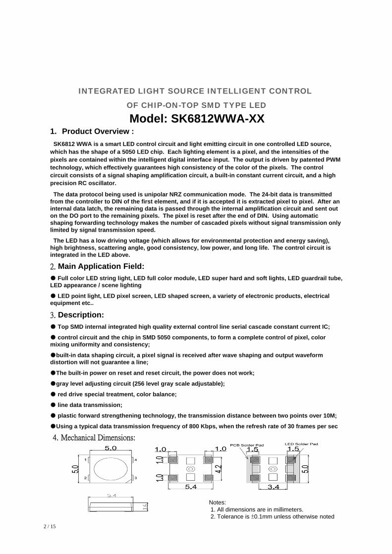
4. Mechanical Dimensions:
Notes:1. All dimensions are in millimeters.2. Tolerance is ±0.1mm unless otherwise noted

SK6812
SK6812 WWA
3 / 15
: The default is the chips with IC integration
-WWA: White Color
W: BW Blue White 6000-7000K
W: WS Warm Sunlight 2700-3000K
A: A Amber 1800-2000K
6. General Information
5. PIN configuration
NO. Symbol Function description 1 VDD Power supply LED
2 DOUT Control data signal output
3 VSS Ground
4 DIN Control data signal input
4 / 15
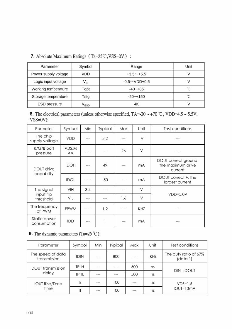
7. Absolute Maximum Ratings(Ta=25℃,VSS=0V) :
Parameter Symbol Range Unit
Power supply voltage VDD +3.5~+5.5 V
Logic input voltage VIN -0.5~VDD+0.5 V
Working temperature Topt -40~+85 ℃
Storage temperature Tstg -50~+150 ℃
ESD pressure VESD 4K V
8. The electrical parameters (unless otherwise specified, TA=-20 ~ +70 ℃, VDD=4.5 ~ 5.5V, VSS=0V):
Parmeter Symbol Min Typical Max Unit Test conditions
The chip supply voltage VDD --- 5.2 --- V ---
R/G/B port pressure
VDS,MAX
--- --- 26 V ---
DOUT drive capability
IDOH --- 49 --- mADOUT conect ground,
the maximum drive current
IDOL --- -50 --- mA DOUT conect +, the largest current
The signal input flip threshold
VIH 3.4 --- --- VVDD=5.0V
VIL --- --- 1.6 V
The frequency of PWM FPWM --- 1.2 --- KHZ ---
Static power consumption IDD --- 1 --- mA ---
9. The dynamic parameters (Ta=25 ℃):
Parameter Symbol Min Typical Max Unit Test conditions
The speed of data transmission fDIN --- 800 --- KHZ The duty ratio of 67%
(data 1)
DOUT transmission delay
TPLH --- --- 500 nsDIN→DOUT
TPHL --- --- 500 ns
IOUT Rise/Drop Time
Tr --- 100 --- ns VDS=1.5IOUT=13mATf --- 100 --- ns
5 / 15
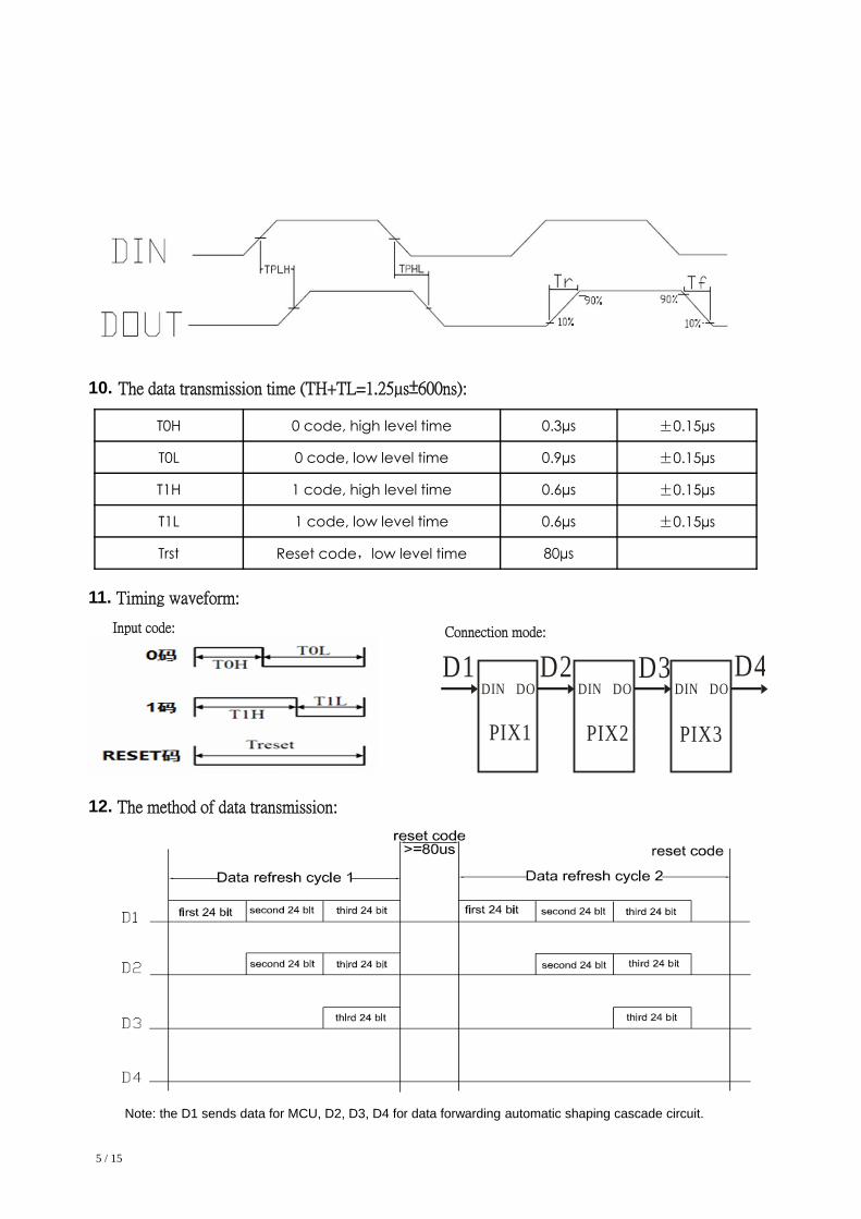
10. The data transmission time (TH+TL=1.25µs±600ns):
T0H 0 code, high level time 0.3µs ±0.15µs
T0L 0 code, low level time 0.9µs ±0.15µs
T1H 1 code, high level time 0.6µs ±0.15µs
T1L 1 code, low level time 0.6µs ±0.15µs
Trst Reset code,low level time 80µs
11. Timing waveform:
DIN DIN DINDO DO DO
PIX1
D1 D2 D3 D4
PIX2 PIX3
Connection mode:Input code:
12. The method of data transmission:
Note: the D1 sends data for MCU, D2, D3, D4 for data forwarding automatic shaping cascade circuit.

6 / 15
13. The data structure of 24bit:
G7 G6 G5 G4 G3 G2 G1 G0 R7 R6 R5 R4R3 R2 R1 R0 B7 B6 B5 B4 B3 B2 B1 B0
Note: high starting, in order to send data (G7 - G6 - ...... ..B0)
14. The typical application circuit:

7 / 15
14. White Color Temperature Ranks & CIE Color Rank (Refer to CIE 1931 chromaticity diagram)
C.A X Y C.A X Y C.A X Y C.A X Y
0.3048 0.3207 0.3028 0.3304 0.3115 0.3391 0.3130 0.3290
0.3130 0.3290 0.3115 0.3391 0.3205 0.3481 0.3213 0.3373
0.3144 0.3186 0.3130 0.3290 0.3213 0.3373 0.3221 0.3261
0.3068 0.3113 0.3048 0.3207 0.3130 0.3290 0.3144 0.3186
0.3068 0.3113 0.3005 0.3415 0.3099 0.3509 0.3144 0.3186
0.3144 0.3186 0.3099 0.3509 0.3196 0.3602 0.3221 0.3261
0.3161 0.3059 0.3115 0.3391 0.3205 0.3481 0.3231 0.3120
0.3093 0.2993 0.3028 0.3304 0.3115 0.3391 0.3161 0.3059
0.3215 0.3350 0.3207 0.3462 0.3290 0.3538 0.3290 0.3417
0.3290 0.3417 0.3290 0.3538 0.3376 0.3616 0.3371 0.3490
0.3290 0.3300 0.3290 0.3417 0.3371 0.3490 0.3366 0.3369
0.3222 0.3243 0.3215 0.3350 0.3290 0.3417 0.3290 0.3300
0.3222 0.3243 0.3196 0.3602 0.3290 0.3690 0.3290 0.3300
0.3290 0.3300 0.3290 0.3690 0.3381 0.3762 0.3366 0.3369
0.3290 0.3180 0.3290 0.3538 0.3376 0.3616 0.3361 0.3245
0.3231 0.3120 0.3207 0.3462 0.3290 0.3538 0.3290 0.3180
C8C7C6C5
D1 D2 D3 D4
D5 D6 D7 D8
C1 C2 C3 C4
CIE chromaticity coordinates (ANSI Cool White)
ANSI Blue White Color bin structures
0.30
0.31
0.32
0.33
0.34
0.35
0.36
0.37
0.38
0.30 0.31 0.32 0.33 0.34
Y
X
C1
6500K
5700K
C2C3
C4
D2D3
D4D1
C5C8
D5D8
C7C6
D6D7
Blue White Graph
8 / 15
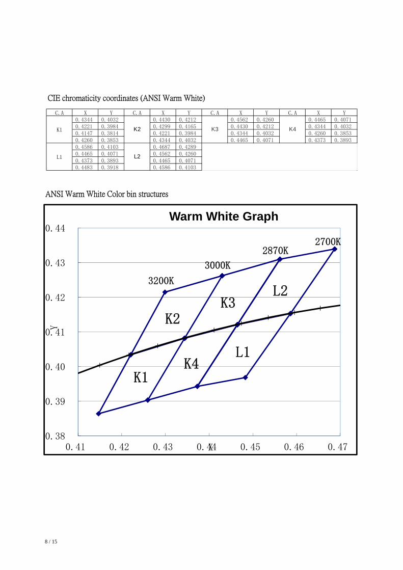
C.A X Y C.A X Y C.A X Y C.A X Y0.4344 0.4032 0.4430 0.4212 0.4562 0.4260 0.4465 0.40710.4221 0.3984 0.4299 0.4165 0.4430 0.4212 0.4344 0.40320.4147 0.3814 0.4221 0.3984 0.4344 0.4032 0.4260 0.38530.4260 0.3853 0.4344 0.4032 0.4465 0.4071 0.4373 0.38930.4586 0.4103 0.4687 0.42890.4465 0.4071 0.4562 0.42600.4373 0.3893 0.4465 0.40710.4483 0.3918 0.4586 0.4103
L1 L2
K1 K2 K3 K4
0.38
0.39
0.40
0.41
0.42
0.43
0.44
0.41 0.42 0.43 0.44 0.45 0.46 0.47
Y
X
3000K
2700K
K2
K4L1
K1
K3L2
2870K
3200K
CIE chromaticity coordinates (ANSI Warm White)
ANSI Warm White Color bin structures
Warm White Graph
9 / 15
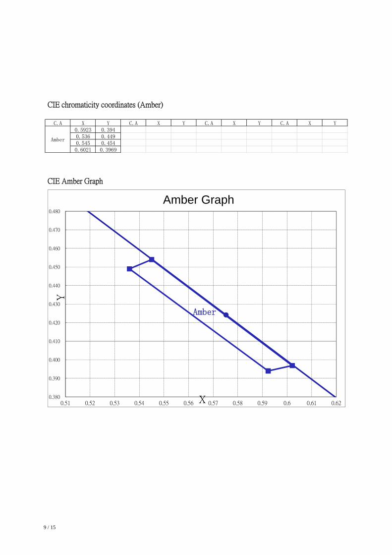
C.A X Y C.A X Y C.A X Y C.A X Y0.5923 0.3940.536 0.4490.545 0.4540.6021 0.3969
Amber
0.380
0.390
0.400
0.410
0.420
0.430
0.440
0.450
0.460
0.470
0.480
0.51 0.52 0.53 0.54 0.55 0.56 0.57 0.58 0.59 0.6 0.61 0.62
Y
X
Amber
CIE Amber Graph
CIE chromaticity coordinates (Amber)
Amber Graph
10 / 15
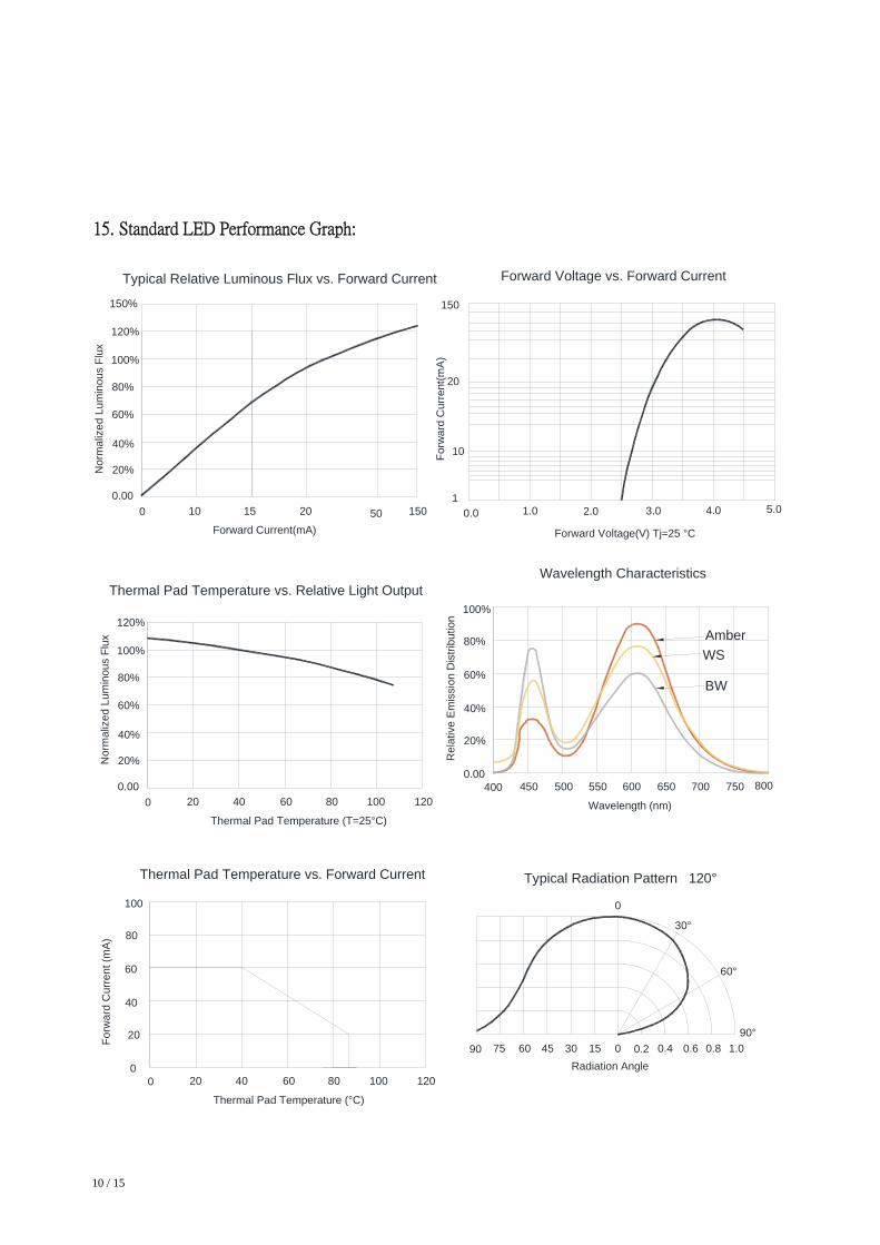
15. Standard LED Performance Graph:
100
20%
0.00
40%
60%
80%
100%
120%
Forward Current(mA)
1.0 2.0 3.0
Forward Voltage(V) Tj=25 °C
No
rma
lize
d L
um
inou
s F
lux
For
wa
rd C
urre
nt(m
A)
Typical Relative Luminous Flux vs. Forward Current Forward Voltage vs. Forward Current
4.01
200 40 60 80 100
20%
0.00
40%
60%
80%
100%
120%
Thermal Pad Temperature (T=25°C)
No
rma
lize
d L
umin
ous
Flu
x
Thermal Pad Temperature vs. Relative Light Output
120
7590 60 45 30 15 0 0.40.2 0.6 0.8 1.0
0
30°
60°
90°
Typical Radiation Pattern 120°
Radiation Angle
10
20
150
15 0.020 50 150
150%
5.0
20
0
40
60
80
100
Fo
rwa
rd C
urr
ent
(m
A)
Thermal Pad Temperature vs. Forward Current
200 40 60 80 100
Thermal Pad Temperature (°C)
120
450400 500 550 600 650
20%
0.00
40%
60%
80%
100%
Wavelength (nm)
Re
lativ
e E
mis
sio
n D
istr
ibut
ion
Wavelength Characteristics
700 750 800
BW
Amber
WS
SK6812 WWA LED
1 1 / 1 5
6
2.0 4.0
Φ1.5
1.7
55
.5
12
0.
8.0
TAPE FEED DIRECTION
CATHODE ID ENTIF ICATION
COVER TAPE
CARRIER TAPE
ESD POLYETHYLENE BAG
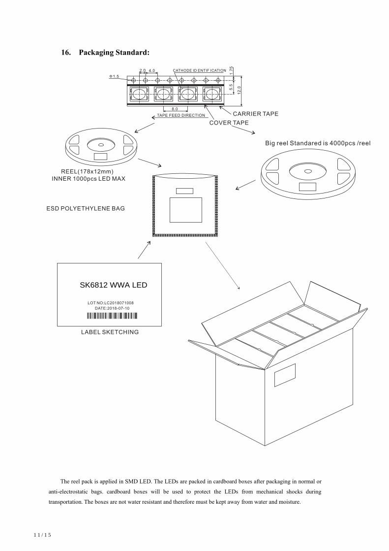
REEL(178x12mm)INNER 1000pcs LED MAX
The reel pack is applied in SMD LED. The LEDs are packed in cardboard boxes after packaging in normal or
anti-electrostatic bags. cardboard boxes will be used to protect the LEDs from mechanical shocks during
transportation. The boxes are not water resistant and therefore must be kept away from water and moisture.
1 . Packaging Standard:
Big reel Standared is 4000pcs /reel
LABEL SKETCHING
DATE:2018-07-10
LOT NO:LC2018071008
1 2 / 1 5
7
7
7
71 . Attention
1 .1 Dust & Cleaning
The LED use silicone glue to package the 5050 Surface, silicone surface can protectoptical properties and improved anti-aging properties. However, silicone is a softer material andprone to attract dust. While a minimal amount of dust and debris on the LED will not causesignificant reduction in illumination.We still need to avoid dust falling on the LED surface. Afteropen the bags it must be used immediately.
When you use trichloroethylene or acetone to clean, sometimes the LED surface willdissolve.
Avoid using organic solvent, it is recommended that isopropyl be used as a solvent forcleaning the LEDs.When using other solvents, it should be confirmed beforehand whether thesolvents will dissolve thepackage and the resin of not.
Do not clean the LEDs by the ultrasonic. When it is absolutely necessary, the influenceas ultrasonic cleaning on the LEDs depends on factors such as ultrasonic power. Baking time andassembled condition.
Before cleaning, a pre-test should be done to confirm whether any damage to the LEDswill occur.
1 .2 Dehumidification
smart led are moisture sensitive components, In IPC/JEDEC J-STD-020MSL Level is 6. No Matter the Package bag is open or not ,The LED must dodehumidification in the oven for 24 hours at 70 degree before use and used within 4 hours,otherwise it need to be dehumidified again
1 .3 Reflow Soldering Characteristics
In our Test, comfirm those smart led are compatible with JEDECJ-STD-020C,Customers are required to follow the soldering temperature profile recommended bythe solder paste manufacturer used.
Please note that this general guideline may not apply to all PCB design and reflowsoldering equipment configurations.
We
1 3 / 1 5
7
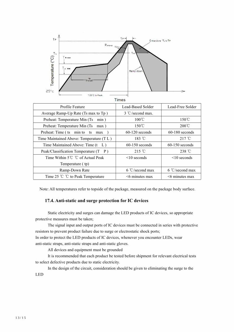
Profile Feature Lead-Based Solder Lead-Free SolderAverage Ramp-Up Rate (Ts max to Tp ) 3℃/second max.Preheat: Temperature Min (Ts min ) 100℃ 150℃Preheat: Temperature Min (Ts max ) 150℃ 200℃Preheat: Time ( ts min to ts max ) 60-120 seconds 60-180 seconds
Time Maintained Above: Temperature (T L ) 183℃ 217℃Time Maintained Above: Time (t L ) 60-150 seconds 60-150 secondsPeak/Classification Temperature (T P ) 215℃ 238℃Time Within 5℃ ℃ of Actual Peak
Temperature ( tp)<10 seconds <10 seconds
Ramp-Down Rate 6℃/second max 6℃/second maxTime 25℃ ℃ to Peak Temperature <6 minutes max <6 minutes max
Note: All temperatures refer to topside of the package, measured on the package body surface.
1 .4. Anti-static and surge protection for IC devices
Static electricity and surges can damage the LED products of IC devices, so appropriateprotective measures must be taken;
The signal input and output ports of IC devices must be connected in series with protectiveresistors to prevent product failure due to surge or electrostatic shock ports;In order to protect the LED products of IC devices, whenever you encounter LEDs, wearanti-static straps, anti-static straps and anti-static gloves.
All devices and equipment must be groundedIt is recommended that each product be tested before shipment for relevant electrical tests
to select defective products due to static electricity.In the design of the circuit, consideration should be given to eliminating the surge to the
LED
1 4 / 1 5
71 .5 Other requirements
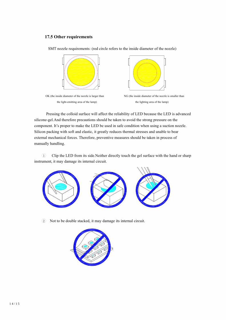
SMT nozzle requirements: (red circle refers to the inside diameter of the nozzle)
OK (the inside diameter of the nozzle is larger than NG (the inside diameter of the nozzle is smaller than
the light-emitting area of the lamp) the lighting area of the lamp)
Pressing the colloid surface will affect the reliability of LED because the LED is advancedsilicone-gel.And therefore precautions should be taken to avoid the strong pressure on thecomponent. It’s proper to make the LED be used in safe condition when using a suction nozzle.Silicon packing with soft and elastic, it greatly reduces thermal stresses and unable to bearexternal mechanical forces. Therefore, preventive measures should be taken in process ofmanually handling.
1 Clip the LED from its side.Neither directly touch the gel surface with the hand or sharpinstrument, it may damage its internal circuit.
2 Not to be double stacked, it may damage its internal circuit.

2
1 5 / 1 5
3 Can not be stored in or applied in the acidic sites of PH<7.
Modify Records
Item NO. Rev. No. Modify ContentSummary
Signature Dat
0