Pushing the limits of DIY electronicsBridging the gap between DIY and professional electronics
14. August 2015
1 / 47

More sophisticated DIY electronics - why?
I professional electronics get more and more sophisticated
I we need to keep up
I you can do really cool things yourselfI Examples:
I hi-speed FPGA boards (with >1GByte/s RAM throughput)e.g. as SDRs, logic analyzers, etc.
I custom networking equipment, e.g. ARM-based routers withGBit ethernet interfaces
2 / 47
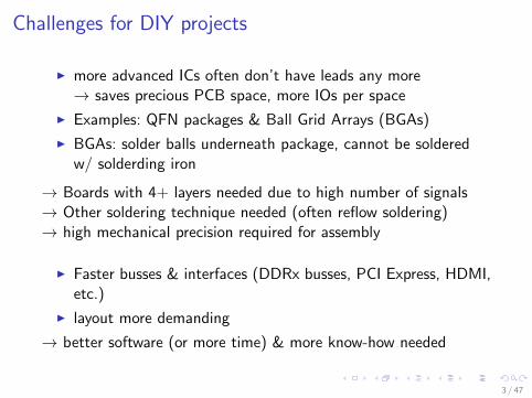
Challenges for DIY projects
I more advanced ICs often don’t have leads any more→ saves precious PCB space, more IOs per space
I Examples: QFN packages & Ball Grid Arrays (BGAs)
I BGAs: solder balls underneath package, cannot be solderedw/ solderding iron
→ Boards with 4+ layers needed due to high number of signals→ Other soldering technique needed (often reflow soldering)→ high mechanical precision required for assembly
I Faster busses & interfaces (DDRx busses, PCI Express, HDMI,etc.)
I layout more demanding
→ better software (or more time) & more know-how needed
3 / 47

In this talk
1. General hints
2. Reflow soldering with solder paste & board assembly
3. hi-speed busses & interfaces (characteristic impedances,length matching)
4. multilayer boards (special stackups required for hi-speed)
5. design software (Eagle & KiCAD, etc.)
4 / 47

General hints
I make a tiny test-board for risky parts like your first DDRxdesign before using it in a complex project
I using outer layers allows fixing things later with copper wire
I use Electroless Nickle Immersion Gold (ENIG) finish forfine-pitch & BGA boards(extremely even surface - contrary to HAL)
I higher soldering temperature needed for Pb-free: 237°C, max.260 (narrow margin)
I some people do BGAs w/o paste, just w/ flux - wouldn’trecommend it as I had problems with that once
I mind the popcorn effect: keep ICs in original pouch withdesiccant & indicator paper - reseal pouches with adhesivetape
5 / 47
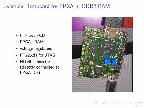
Example: Testboard for FPGA + DDR2-RAM
I tiny test-PCB
I FPGA+RAM
I voltage regulators
I FT2232H for JTAG
I HDMI connector(directly connected toFPGA IOs)
6 / 47

Soldering
basically 3 options:I Reflow oven
I modified pizza oven (more heat, temperature control)I cheap oven from china (modified)I Problem: black surfaces (IC packages, connectors) absorb more
IR radiation from quartz lamps than metal surfaces→ temperature on PCB varies with location
I hot air gun with hot plateI cheap hot air guns availableI problem: hard to tell when BGA balls meltI problem: large copper areas won’t get suffiently hot w/o
preheaterI hot plates for cooking can be used as cheap preheatersI set them to (100-120 °C)I check PCB surface w/ IR thermometer
7 / 47

Soldering (2)
I Vapor phaseI special liquid which boils at high temperature (230-240°C)I great soldering methodI good heat transfer - PCB rests in vapor phase, not in liquidI overheating ICs is difficultI BUT: if it does get too hot, very bad things will happen
(hydrofluric acid & stuff, seehttp://www.heise.de/make/meldung/
Dampfphasen-Medium-in-Kleinmengen-1780946.html
(german))I liquid is very expensive but you won’t need much per runI you need a high pot (e.g. pot for asparagus)I several DIY projects, haven’t tried it myself yet
8 / 47

Soldering: Reflow oven
I T962 from china
I small holding capacity, but high heating power (often aproblem w/ pizza ovens)
I LPC2134 arm controller - not read-protected!
I did a dump of the firmware, reverse-engineered it
I wrote my own firmware - temperature controller implementedon a PC
I connection to oven using 3.3V RS232
I only few commands: heat, read temperature, run fan
I host-code done in Lua - easy to adapt or add newtemperature profiles
I tiny firmware runs completely from RAM
I code: https://github.com/znuh/t962some documentation will follow
9 / 47

Soldering: T962 oven
I masking tape should be replaced w/ kapton tape (heatresistance)
I for my alternative firmware 3.3V RS232 Rx&Tx pinheaders
I external reset & boot buttons (for bootloader invocation)
I add pullup resistors for triacs - otherwise fan & heaters willbe on while in bootloader!
I spacers for PCB (e.g. screw nuts)
I measure temperature directly on PCB (K-type sensors are wellsuited)
I do some test-runs first
I more docs (in german): https://www.mikrocontroller.net/topic/310148#3649461
10 / 47

Soldering: T962 oven (2)
11 / 47
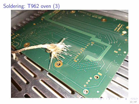
Soldering: T962 oven (3)
12 / 47

Soldering: T962 oven (4)
13 / 47

Solder paste
I solder paste: tiny solder balls embedded in flux
I for fine-pitch & BGAs you need a stencil
I paste is forced through openings of stencil
I some PCB houses offer free stencils for your boards (e.g.pcb-pool), others don’t
I sometimes a single-layer dummy-PCB + free stencil fromanother PCB house is cheaper than a non-free stencil fromthe house you get your PCBs from
14 / 47
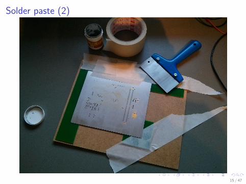
Solder paste (2)
15 / 47

Solder paste (3)
16 / 47
Solder paste (4)
I you need to fix the stencil firmly to the PCB so that you canfold up the stencil after printing
I there are fixing-kits for this, you can also make sth. yourself
I stir paste well before use, keep in refrigerator - paste is usuallygood for about 1 year
I if a tiny paste droplet covers two adjacent pads it’s not alwaysa problem - tiny amounts will flow to where they should beduring solder process
I cleaning a stencil works well with lighter fluid
I if you mess up the printing you can clean the PCB and startover
I wear a lab coat - paste will get everywhere and getting it outof your clothes is a challenge
17 / 47

Placing & aligning parts
I place most challenging parts (BGAs, QFNs) first, easy partslater
I if you smeared the paste too much to fix clean the PCB &parts, start over
I for BGAs and QFNs place a rectangle around the chip in thesilkscreen
I helps a lot with the alignment
I use a tweezer for picking & placing the chips
I vacuum tweezers: only recommended with electric pump
I place chip softly on solder paste
I align chip carefully, inspect w/ magnifying glass
I push chip slightly down
18 / 47

Placement helper for eagle
I hacked a quick components placement helper for eagle board
I needs Lua, LuaXML, lgi (Lua GObject Introspection) with Gtkand Cairo
I only tested on Linux
I lgi is (Windows) / might be tough to install on other OSes
I code: https://github.com/znuh/pcbtools
I usage: lua gui.lua board.brd
I easy to use
I basically translates Eagle XML elements to Cairo calls
I eats RAM for breakfast (1 cairo surface per layer)
19 / 47

Placement helper for eagle
20 / 47

Hi-speed busses & interfaces
I signal integrity for high-speed signals is a challengeI length-matching needed
I propagation speed/delay depends on the dielectricconstant εr of the insulator
I rule of thumb for PCBs: 6ps/mm for top/bottom, 7ps/mm forinner layers
I signals in inner layers are approx. 20% slower than ontop/bottom!
I not respected by eagle, vias not considered eitherI eagle measures full length of tracks, not just between ICs
(termination resistors usually after ICs)
I transmission lines with characteristic impedance neededI special multilayer stackupsI width of PCB tracks depend on multilayer stackup
21 / 47

Length matching tool for eagle
I https://github.com/znuh/pcbtools
I work in progress, no documentation
I uses Lua, needs LuaXML
I edit delay config.lua
I lua -i bga workshop.lua - starts interactive Lua session
I load brd(’myboard.brd’) loads eagle board
I get signal delays(’U1’, ’IC4’) shows adjusted metricdistance for signals between IC4 and U1
I get signal delays(’U1’, ’IC4’, ’time’) shows time delay forsignals between IC4 and U1
22 / 47

Length matching tool for eagle: screenshot
23 / 47

Characteristic impedance Z0
I high frequency signals travel through conductors like a wave
I transmission line model with capacitance C ′ & inductance L′
I these values depend on the geometry of the transmissionline
I characteristic impedance Z0 =√
L′
C′ (with losses ignored)
I signal reflected at end of transmission line if not properlyterminated
I reflected signals can travel back and forth destroying thesignal integrity
I proper termination with resistor equivalent to characteristicimpedance (remember 10Base2?)
24 / 47

Transmission lines
I a few more details: termination & slew rate
I simulating transmission lines
I designing transmission lines for a given impedance
I multilayer stackups for transmission lines
25 / 47

Termination schemes
I mostly on-die termination for point-to-point signals like LVDS
I termination may be needed for multipoint connections
I stubs are very bad - avoid them, place termination after last IC
I DDR2/3 memory has builtin termination (ODT) for databusses
I clock and control/address lines need extra termination
I for control/address lines you might get away without anytermination
I for synchronous signals reducing clock frequency can help(signals have more time to settle before clock edge)
26 / 47

Frequency vs. slew rate
I Simply reducing the frequency of a transmission doesn’timprove the signal quality
I Why?I Reducing the frequency doesn’t reduce the slew rateI slew rate: time for a signal to go from low to hi (trise) or vice
versa (tfall)I slew rate always has higher frequency portions than base
frequency of transmission (see spectrum of a square wave)I short/fast slew rates are needed for high frequencies
(otherwise signal doesn’t reach hi/low state in time)I more details: http://www.mikrocontroller.net/
articles/Wellenwiderstand (german) 27 / 47

Finding the slew rate
I sometimes trise and tfall given in datasheet
I time from 10% of hi level to 90% of hi level
I professional tools use IBIS data: Input/Output BufferInformation Specification
I these files are textfiles, contain waveform data
I e.g. waveform for output buffer driving a 50Ω transmission line
I can be used to simulate & analyze signal integrity with giventransmission line & termination
I easy to read and plot (e.g. w/ gnuplot)
28 / 47

Simulating transmission lines
I SPICE is usually used for electronics simulation
I SPICE is just the engine, no user interface
I easy to use, free as in beer user interface: LTspicehttp://www.linear.com/designtools/software/
I download without registration - thank you Linear! <3
I Windows & OSX versions available, windows version worksvery well with wine
I you can find tutorials on the web
Two open-source projects for using IBIS with SPICE:
I https://github.com/russdill/darter
I http://www.thedigitalmachine.net/eispice.html
Haven’t tried them yet
29 / 47
Simulating transmission lines with LTspice
I use a PULSE voltage sourceI insert trise and tfallI OR: use a PWL file (time/value text file)I can be easily generated from IBIS file
I add a transmission line (tline)I Td: electrical length
simulating the longest line of a bus is usually sufficientI Z0: characteristic impedance
I add input buffer and terminationI capacitance of input buffer important - see datasheetI often on-die termination with Z0 available for hi-speed signalsI for unterminated inputs: usually 1MΩ
30 / 47

LTspice demo
31 / 47

Z0 mismatchNo termination:
Z0 = 75Ω with 50Ω termination:
32 / 47

Z0 mismatch (2)
Z0 = 100Ω with 50Ω termination:
I Z0 doesn’t need to be spot-on
I signal gets gradually worse as mismatch grows
I specifications often allow ± 20%
I we try to hit Z0 as good as possible
33 / 47

Designing transmission lines for a given Z0
I always at least one low-impedance reference plane neededcan be GND or Vdd - GND is better (less noise)
a) b) c)
I a: (asymmetric/offset) stripline: for inner layers - 2 referenceplanesasymmetric/offset: unequal distance to reference planes
I b: (coated) microstrip: for outer layerscoated: w/ solder mask above the conductor
I c: coplanar waveguide (CPW): good for analog signals,normally not used for busses (space requirements)optional additional ground plane
34 / 47

Designing transmission lines for a given Z0 (2)
a) b) c)
I a: (asymmetric/offset) stripline: for inner layers - 2 referenceplanesasymmetric/offset: unequal distance to reference planes
I b: (coated) microstrip: for outer layerscoated: w/ solder mask above the conductor
I c: coplanar waveguide (CPW): good for analog signals,normally not used for busses (space requirements)optional additional ground plane
I Z0 depends mostly on:I width w of conductor: increasing w → lower Z0
I height h (h1/h2) of conductor above reference plane(s):decreasing h→ lower Z0
I dielectric constant εr of insulators: higher εr → lower Z0
35 / 47

Differential transmission lines
I differential lines often used for hi-speed signals (Ethernet,LVDS, PCI Express, SATA, etc.)
I more robust to noise
I driven with inverse polarity (P: positive, N: negative)
I receiver utilizes difference between P&N
I noise couples into both lines, doesn’t change difference
I differential impedance Zdiff : usually 2* Z0
I more details: http://www.polarinstruments.com/support/cits/AP157.html
I Zdiff depends on Z0 of individual lineslower Z0 → lower Zdiff
I distance s between conductors: lower s→ lower Zdiff
36 / 47

Some notes re: transmission lines
I trapezoid shape tracks produced due to etch-back
I etch-back usually equal to copper height
I affects differential pairs more than single-ended
I εr for FR-4 PCBs frequency-dependent - 4.2 usually is a goodvalue
I microstrips see a mix of air soldermask and FR-4 εrI soldermask height above PCB and conductors depends on
PCB house
I example values: 42um above PCB, 15um above conductorsource: http://www.we-online.de/web/de/index.php/show/media/04_leiterplatte/2013_1/webinare_1/
signalintegritaet/Webinar_Signal_final.pdf
37 / 47

Calculating w, h and Z0
I there are approximation equations
I various javascript implementations
I e.g.: http://www.leiton.de/leiton-tools-impedance-capacity-calculator.html
I KiCAD has a builtin calculator (pcb calculator)
I more precise: field solver
I open source 2D solver: atlchttp://atlc.sourceforge.net/
I input data: windows BMP files
I no GUI, console tool - takes a while depending on BMP size
I mdtlc: free (beer) windows GUI with builtin atlc backend (oldatlc version though) http://mdtlc.sourceforge.net/
38 / 47

atlc
I transmission line images from previous slides are atlc inputimages
I calculates signal propagation speed, single-ended anddifferential impedance
I bitmaps can be generated with console tools
I or with a simple graphics library like GD
I red, blue and green for P, N and reference conductors
I other colors for insulators - custom εr values can be mappedto custom colors
I ratio between h, w, s, etc. important - actual scale doesn’tmatter as long as it’s fine enough
I e.g. 1px for 5um, larger images are more accurate but takemore CPU-time
39 / 47

some of my tools
I work in progress, crappy, started a rewrite
I Lua code, no documentation yet
I https://github.com/znuh/pcbtools
I config.lua: multilayer stackup definitions, requiredimpedances - edit these
I then run lua -i impedance.lua (interactive Lua session)
I will give you quick results using approximation equations
I generates a visualization of stackup as stackup.png
I run atlc(name, layer id, w, s) can be used to generate aBMP and run atlc (s only for differential signals)
I needs lua-gd and convert from imagemagick, BMPs generatedin atlc/ subdir
I units in mm, layer id needs to be a signal-layer, not areference layer
I example: run atlc(”pcie”,2,0.25,0.25)
40 / 47

Multilayer stackups
I height h between layers depends on multilayer stackup
I we need to choose a multilayer stackup which gives us good hvalues
I custom stackups are quite expensive (manufacturer has toproduce a full panel just for you)→ we need to choose a PCB house with a suitable poolstackup
I ensure that PCB manufacturer won’t use another stackup foryour pool order - talk to your PCB house before design &production!
I controlled impedance: manufacturer guarantees certain Z0
±x - expensive, not in pool, we can do without
41 / 47
Multilayer stackups (2)
I you usually want to use top/bottom as signal layers so youcan patch signals later if necessary
I that means adjacent layers should be reference layers if youwant to use microstrips
I solid copper planes in layer stack need to be symmetric(copper balance)
I Vdd planes close to GND are good because they form a goodcapacitor for HF
I with less than 8 layers h often is very high
I this results in rather large track widths w for Z0 = 50Ω
I might lead to space issues during routing
I we need to make trade-offs (e.g. slight Z0-mismatch ornon-adjacent Vdd/GND layers)
42 / 47

Multilayer stackups - examples
left to right:pcb-pool ML6, WE-direkt pool ML6, eurocircuits pool ML8
43 / 47

PCB manufacturers - some examples (mostlyEurope/Germany)
I Eurocircuits: http://www.eurocircuits.com/ - poolavailable for up to 8 layers, detailed stackup view, guaranteedstackup
I Leiton: http://www.leiton.de/ - pool for up to 8 layers
I PCB-pool: http://www.pcb-pool.com/ - pool for up to 6layers, free stencil and ENIG, you need to ask for thedesignated pool stackup
I WE direkt: http://www.wedirekt.de/index.php/pcb -pool for up to 8 layers, small additional fee for guaranteedpool stackup
44 / 47

Dogbone breakout for BGAs
I divide pads in 4quadrants
I place 0.2mm viasbetween pads
I place 0402 decouplingcaps in via-free zone
I works well with pitch≥ 0.8mm
I ensure to cover vias with solder stop(in eagle: Masks / Limit: set to > via size, check tStop layer)
I minor clearance violations usually no problem(e.g. 0.1125mm instead of 0.125mm)
45 / 47

Design software
I Eagle: http://www.cadsoftusa.com/eagle-pcb-design-software/about-eagle/
I hobbyist version for non-commercial projects with ≤ 6 layers
I XML boardfiles easy to read, understand & modify
I KiCAD: http://www.kicad-pcb.org/
I free & open-source
I make sure to use devel version, not stable(lots of new features) - save often, make backups!
I layout engine very powerful, push&shove, etc.better suited for more complex projects
I builtin python interpreter
I boardfiles: textfiles, easy to read, understand & modify
I builtin 3d viewer
46 / 47

Conclusion
I lack of expensive professional software can be compensatedfor with free/open source software, custom tools, knowledgeand a high motivation
I reasonably priced pool PCBs can be used for very advancedprojects
I reflow soldering can be done without expensive equipment too- needs some experiments & patience
further strategy:
I write & improve software
I build & provide reflow equipment in hackerspaces
I collaborate
more questions? DECT: hunz (i’m in the Koniglich BayerischesAmtsvillage - the thing with the bavarian flags)
47 / 47