U.P.B. Sci. Bull., Series C, Vol. 76, Iss. 2, 2014 ISSN 2286 – 3540
PARAMETER EXTRACTION FOR A NEW ANALYTICAL MODEL OF THE SHORT-CHANNEL MOS TRANSISTOR
Andrei SEVCENCO1, Cristian BOIANCEANU2
An extraction method for the parameters of a new analytical model of the submicron MOS transistor for analog applications is presented. The stages which form the extraction process are detailed, along with an original parameter extractor created in Labview, which uses the Levenberg-Marquardt fitting algorithm. Also presented are the results of the fitting of the model to experimental curves obtained with measured data taken from real MOS transistors, as well as to theoretical curves generated with the EKV model.
Keywords: analytical modeling, parameter extraction, short-channel effects, MOS
transistor, fitting algorithm.
1. Introduction
Modeling the MOS transistor has been, for more than 30 years, a continuous objective of the entire electronics scientific community [1]. This is because having accurate descriptions of transistor behavior before actual production of the integrated circuits streamlines costs and hastens product release to market. As the microelectronics technology progressed and integrated circuits migrated towards VLSI (Very Large Scale Integration), the classical models, which describe the behavior of the MOS transistor, had to be updated in order to accurately explain the experimental observations [1]. The models became more complex and the need for computer assisted design appeared, especially because the computations needed by the models became so extensive that solving the equation systems by hand was not feasible.
One very important part of model development and subsequent use in integrated circuit design is the extraction of the model parameters. This is done for each fabrication technology to which a certain model is applied, because the model has to be fitted to each technology’s specific physical characteristics. Since models have been constructed, in recent years, to account for the more complex behaviors of submicron MOS transistors currently used in all areas of microelectronics, even analytical models start to need computer assisted parameter extraction.
1 University POLITEHNICA of Bucharest, Romania, e-mail: [email protected] 2 University POLITEHNICA of Bucharest, Romania, e-mail: [email protected]
132 Andrei Sevcenco, Cristian Boianceanu
Many commercial software solutions exist to solve this requirement, but customized parameter extractors, specifically made for a certain model are always a better fit.
This paper presents a parameter extraction method used for a new analytical model of the submicron MOS transistor for analog applications. Along with a few other procedures, the parameter extractor is used in the validation [3, 4] of the new analytical model by fitting the model’s expressions to experimental electrical characteristics measured on real MOS transistors and theoretical curves generated with the BSIM3 and EKV models.
The parameter extractor uses the Levenberg-Marquardt fitting algorithm [5, 7]. This fitting algorithm was chosen due to its excellent performance in fitting arbitrary functions and the high speed of convergence, while keeping an acceptable accuracy of optimization.
2. A new model of the MOS transistor for analog applications [3, 4]
A new analytical model of the MOS transistor for analog applications was developed in [3,4]. This model succeeds in integrating the combined action of the most important short-channel effects, the carrier velocity saturation and mobility degradation effects, on MOS transistor conduction. Because it was built as an extension of the standard MOS model, the proposed model also offers relatively simple equations for the drain current in the linear and active regions, which are reduced to the expressions of the standard model when certain parameters are considered negligible.
The expressions contained in the model’s system explain the MOS conduction from the electrical point of view, by replacing electric fields with voltages applied to the various terminals of the device.
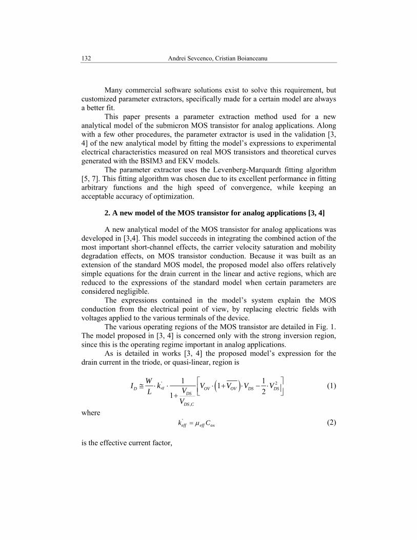
The various operating regions of the MOS transistor are detailed in Fig. 1. The model proposed in [3, 4] is concerned only with the strong inversion region, since this is the operating regime important in analog applications.
As is detailed in works [3, 4] the proposed model’s expression for the drain current in the triode, or quasi-linear, region is
( )' 2
,
1 1121
effD OV OV DS DSDS
DS C
WI k V V V VVLV
⎡ ⎤≅ ⋅ ⋅ ⋅ + ⋅ − ⋅⎢ ⎥⎣ ⎦+ (1)
where 'eff eff oxk Cμ= (2)
is the effective current factor,
Parameter extraction for a new analytical model of the short-channel MOS transistor 133
,2OV
OVT GS C
VVV V
=+
(3)
is the normalized overdrive voltage (VOV = VGS - VT ) and
,DS c cV aLξ= (4) is the critical drain voltage, i.e. the drain voltage value at which carrier velocity saturation is the dominant short channel effect in the transistor. In eq. (2)
( )0
2
,
12 11
effT
OVGS C
V VV
μμ = ⋅++
(5)
is the effective carrier mobility. The critical gate voltage, VGS,C, is defined as
, ,6GS C x c oxV tξ= (6) where ξx,c is the critical transverse electric field and tox is the gate oxide thickness.
Fig.1. Operating regions of the MOS transistor
134 Andrei Sevcenco, Cristian Boianceanu
By differentiating eq. (1), we obtain the expression of the drain voltage at the point of intersection between the quasi-linear region and the active region, VDS,act
( ), ,,
1 2 1 1OVDS act DS C OV
DS C
VV V VV
⎛ ⎞= + ⋅ + −⎜ ⎟⎜ ⎟
⎝ ⎠ (7)
In order to obtain the drain current expression in the active region, the expression of VDS,act is substituted for VDS in expression (1)
2,' 2
, , 2,
12
DS actD eff DS act D C
DS C
VWI k V IL V
= ⋅ = (8)
where ' 2
, ,12D C eff DS C
WI k VL
= ⋅ (9)
is the critical drain current. From eq. (8) we can see that, when VDS,act = VDS,C we get ID = ID,C. Therefore, ID,C is the drain current at the point when the channel enters into velocity saturation dominance.
By adding the channel length modulation effect to eq.(8), we obtain the finalized expression for the active mode region
2
, ,, 2
,
1DS act DS DS actD D C
DS C A
V V VI I
V V−⎛ ⎞
= ⋅ ⋅ +⎜ ⎟⎝ ⎠
(10)
In analog integrated circuits, the most important parameter of any
transistor is its transconductance [1]. This is because transconductance is the measure of a devices amplification function, by quantifying the transfer efficiency from input to output.
By using expressions (7) and (8) and differentiating the drain current with respect to VGS, we obtain the transconductance equation for the active region
( ) ( ),
, ,
211 11 2 1 1 2 1 1
OVDm m c
GS OV OVOV OV
DS C DS C
VdIg gdV V VV V
V V
⎛ ⎞⎛ ⎞⎜ ⎟⎜ ⎟⎜ ⎟⎜ ⎟= = − +⎜ ⎟⎜ ⎟⎜ ⎟⎜ ⎟+ ⋅ + + ⋅ + +⎜ ⎟⎜ ⎟⎝ ⎠⎝ ⎠
(11)
where
Parameter extraction for a new analytical model of the short-channel MOS transistor 135
', ,m c eff DS C
Wg k VL
= (12)
is the maximum value of the transconductance. This value of transconductance is practically independent of the channel length modulation effect because
,DS act AV V<< . By rearranging and substituting the relevant terms within eq. (11) with their expressions we obtain a transconductance expression dependent on drain current
,,
, ,,
1 121
DS CDm m c
D C T GS CD C D
VIg gI V VI I
⎛ ⎞⎜ ⎟= +⎜ ⎟++ ⎝ ⎠
(13)
However, one very important step in the development of any analytical
model is the verification of its capabilities and real-world performance. And this can only be done experimentally, by subjecting the model to comparisons to real data, measured on real transistors and theoretical curves generated by other models.
In the following paragraphs, we will detail the experimental setup, the data analysis method, the parameter extractor architecture and user interface and a series of theory - experiment comparisons to prove the efficacy of the parameter extraction process and model-fitting algorithm.
3. Electrical characteristics measurement experiment
The model described in paragraph 2 is validated by comparison to experimental data measured on MOS devices. The MOS transistors that were measured to obtain the data were n and p type MOSFETs with aspect ratios (W/L) of 5.62/0.6 and 0.7/0.6, fabricated in an industry standard CMOS technology in the 0.22μm node. The measurements were made at room temperature, on test structures, by using an HP4145B Semiconductor Parameter Analyzer and a micromanipulator with a vacuum pump. The test structures were fixed on a silicon wafer, in order to ensure flatness between test pads.
The 4145b analyzer was considered adequate to the purpose of the experiment due to its satisfactory measurement capabilities. This tool can measure currents in the picoampere to 100mA range with a maximum error of ±1.8%. In addition, the sampling rate of 150 measurements per second allowed for a fast and comfortable experimental data collection process. Of benefit are the capability of the 4145b to communicate with the computer over the GPIB interface and the ease of use of its embedded interface.
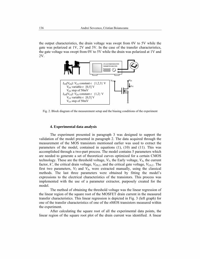
The measurement setup and the biasing procedure used in the experiment are presented in Fig. 2. The biasing conditions were varied on the gate and drain terminals, while the source terminal was tied to ground, along with the bulk. For
136 Andrei Sevcenco, Cristian Boianceanu
the output characteristics, the drain voltage was swept from 0V to 5V while the gate was polarized at 1V, 2V and 3V. In the case of the transfer characteristics, the gate voltage was swept from 0V to 5V while the drain was polarized at 1V and 2V.
Fig. 2. Block diagram of the measurement setup and the biasing conditions of the experiment
4. Experimental data analysis
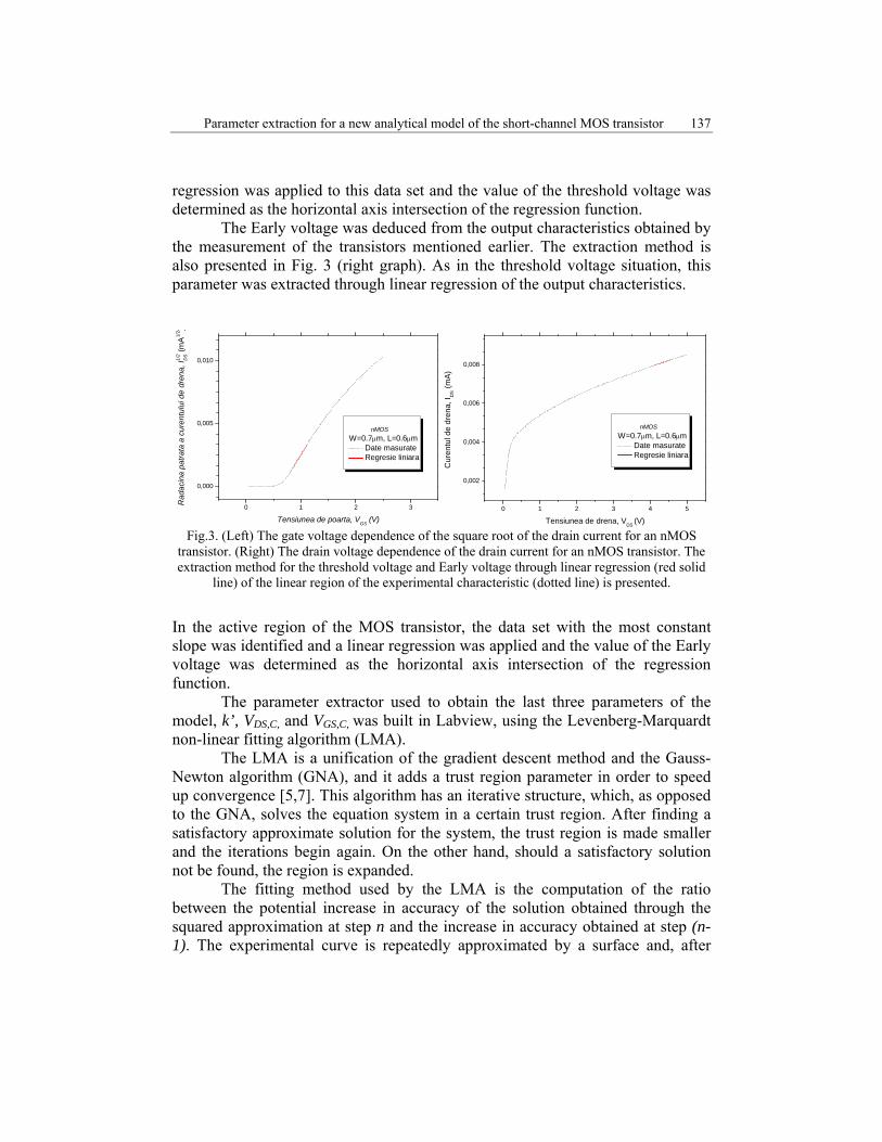
The experiment presented in paragraph 3 was designed to support the validation of the model presented in paragraph 2. The data acquired through the measurement of the MOS transistors mentioned earlier was used to extract the parameters of the model, contained in equations (1), (10) and (11). This was accomplished through a two-part process. The model contains 5 parameters which are needed to generate a set of theoretical curves optimized for a certain CMOS technology. These are the threshold voltage, VT, the Early voltage, VA, the current factor, k’, the critical drain voltage, VDS,C, and the critical gate voltage, VGS,C. The first two parameters, VT and VA, were extracted manually, using the classical methods. The last three parameters were obtained by fitting the model’s expressions to the electrical characteristics of the transistors. This process was implemented with the use of a parameter extractor, purposely created for the model. The method of obtaining the threshold voltage was the linear regression of the linear region of the square root of the MOSFET drain current in the measured transfer characteristics. This linear regression is depicted in Fig. 3 (left graph) for one of the transfer characteristics of one of the nMOS transistors measured within the experiment.
After calculating the square root of all the experimental data points, the linear region of the square root plot of the drain current was identified. A linear
IDS(VDS): VGS constant є {1,2,3} V VDS variable є [0,5] V VDS step of 50mV IDS(VGS): VDS constant є {1,2} V VGS variable є [0,5] V VGS step of 50mV
Parameter extraction for a new analytical model of the short-channel MOS transistor 137
regression was applied to this data set and the value of the threshold voltage was determined as the horizontal axis intersection of the regression function.
The Early voltage was deduced from the output characteristics obtained by the measurement of the transistors mentioned earlier. The extraction method is also presented in Fig. 3 (right graph). As in the threshold voltage situation, this parameter was extracted through linear regression of the output characteristics.
0 1 2 3
0,000
0,005
0,010
nMOSW=0.7μm, L=0.6μm
Date masurate Regresie liniara
Rad
acin
a pa
trata
a c
uren
tulu
i de
dren
a, I1/
2D
S (m
A1/
2 )
Tensiunea de poarta, VGS (V)0 1 2 3 4 5
0,002
0,004
0,006
0,008
nMOSW=0.7μm, L=0.6μm
Date masurate Regresie liniara
Cur
entu
l de
dren
a, I D
S (m
A)
Tensiunea de drena, VDS (V) Fig.3. (Left) The gate voltage dependence of the square root of the drain current for an nMOS
transistor. (Right) The drain voltage dependence of the drain current for an nMOS transistor. The extraction method for the threshold voltage and Early voltage through linear regression (red solid
line) of the linear region of the experimental characteristic (dotted line) is presented.
In the active region of the MOS transistor, the data set with the most constant slope was identified and a linear regression was applied and the value of the Early voltage was determined as the horizontal axis intersection of the regression function. The parameter extractor used to obtain the last three parameters of the model, k’, VDS,C, and VGS,C, was built in Labview, using the Levenberg-Marquardt non-linear fitting algorithm (LMA).
The LMA is a unification of the gradient descent method and the Gauss-Newton algorithm (GNA), and it adds a trust region parameter in order to speed up convergence [5,7]. This algorithm has an iterative structure, which, as opposed to the GNA, solves the equation system in a certain trust region. After finding a satisfactory approximate solution for the system, the trust region is made smaller and the iterations begin again. On the other hand, should a satisfactory solution not be found, the region is expanded. The fitting method used by the LMA is the computation of the ratio between the potential increase in accuracy of the solution obtained through the squared approximation at step n and the increase in accuracy obtained at step (n-1). The experimental curve is repeatedly approximated by a surface and, after
138 Andrei Sevcenco, Cristian Boianceanu
solving the linear system, the correction applied to the model and the accuracy estimation are adjusted. The strength of the LMA is contained in the use of a parameter, λ, which sets the trust region size.
The complete expression of the algorithm is [5,7]
( )( ) ( )T T TJ J diag J J J y f⎡ ⎤+ λ ⋅ δ = − β⎣ ⎦ (14)
where J is the Jacobian matrix with row i equal to iJ , f and y are the vectors with their ith elements equal to f(xi, β) and yi, respectively, and δ is the parameter estimation. β is the initial guess of the parameter vector.
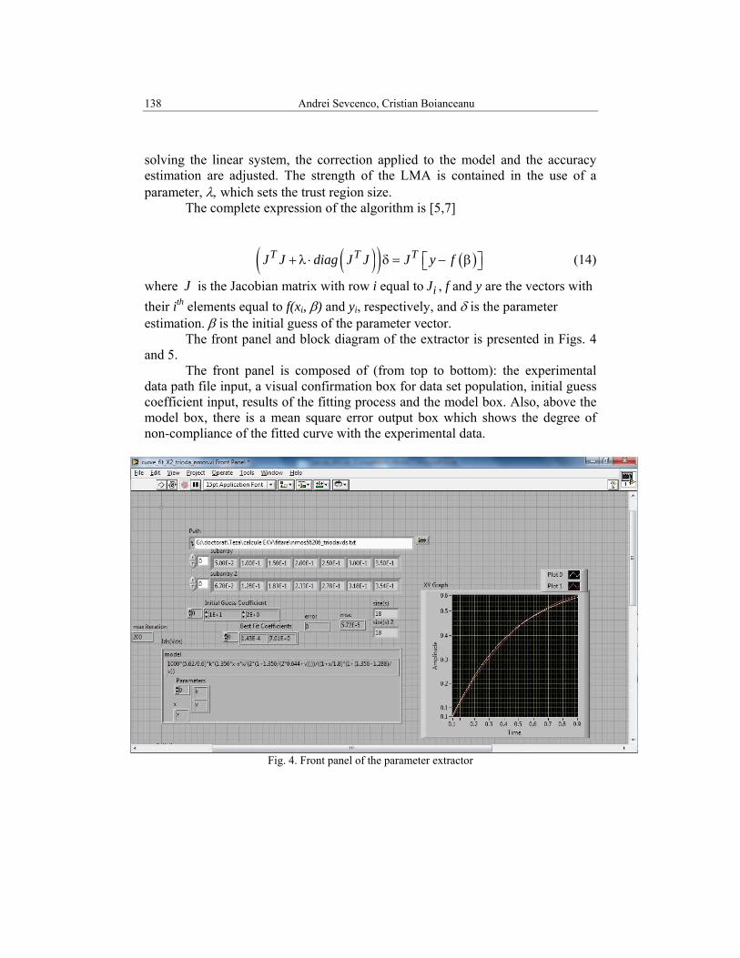
The front panel and block diagram of the extractor is presented in Figs. 4 and 5.
The front panel is composed of (from top to bottom): the experimental data path file input, a visual confirmation box for data set population, initial guess coefficient input, results of the fitting process and the model box. Also, above the model box, there is a mean square error output box which shows the degree of non-compliance of the fitted curve with the experimental data.
Fig. 4. Front panel of the parameter extractor
Parameter extraction for a new analytical model of the short-channel MOS transistor 139
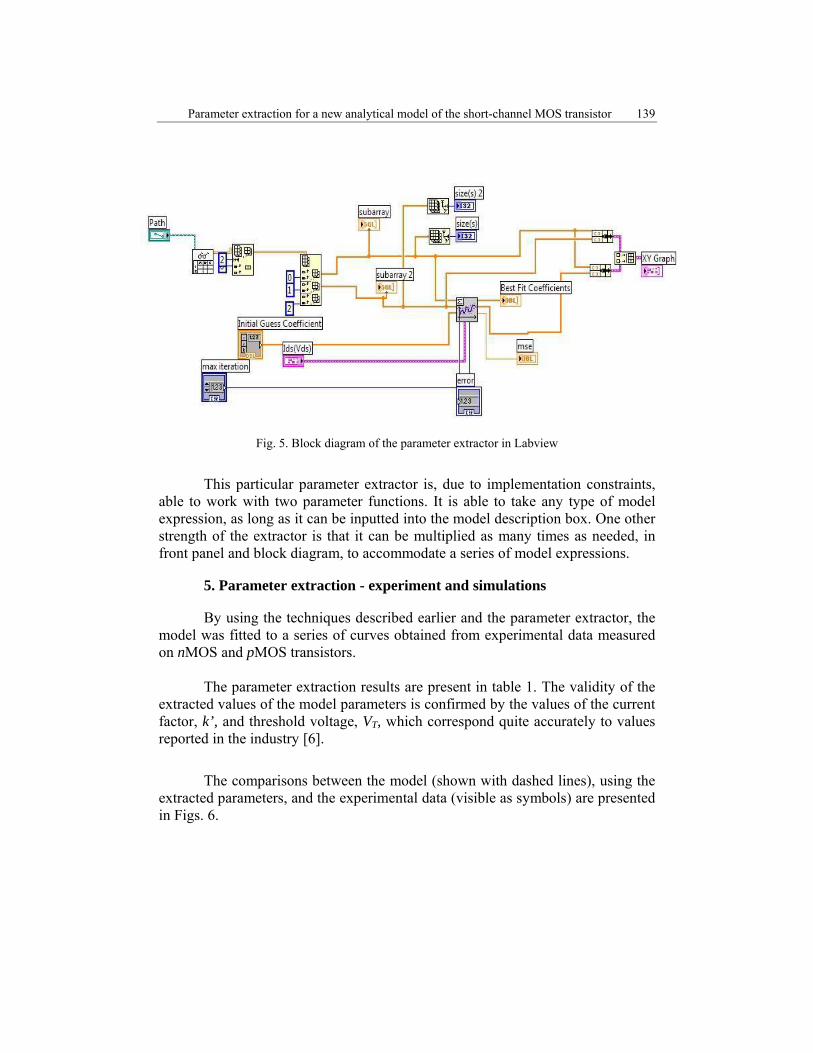
Fig. 5. Block diagram of the parameter extractor in Labview
This particular parameter extractor is, due to implementation constraints,
able to work with two parameter functions. It is able to take any type of model expression, as long as it can be inputted into the model description box. One other strength of the extractor is that it can be multiplied as many times as needed, in front panel and block diagram, to accommodate a series of model expressions.
5. Parameter extraction - experiment and simulations
By using the techniques described earlier and the parameter extractor, the model was fitted to a series of curves obtained from experimental data measured on nMOS and pMOS transistors.
The parameter extraction results are present in table 1. The validity of the
extracted values of the model parameters is confirmed by the values of the current factor, k’, and threshold voltage, VT, which correspond quite accurately to values reported in the industry [6].
The comparisons between the model (shown with dashed lines), using the extracted parameters, and the experimental data (visible as symbols) are presented in Figs. 6.
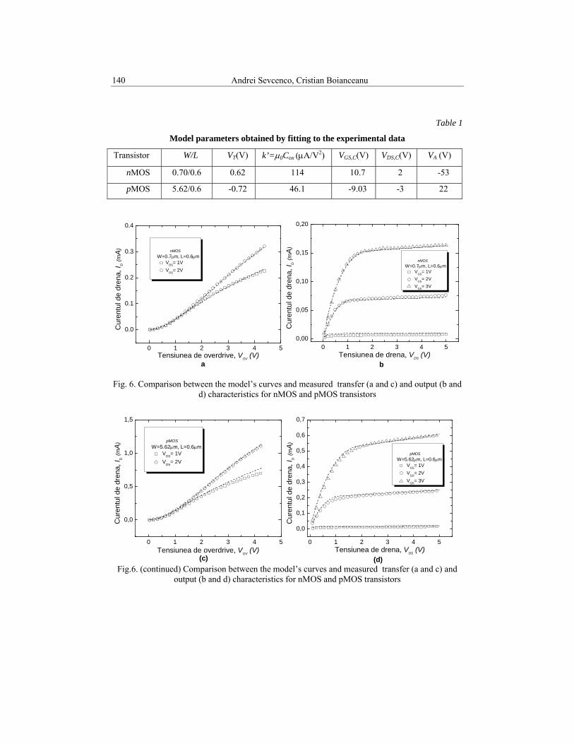
140 Andrei Sevcenco, Cristian Boianceanu
Table 1
Model parameters obtained by fitting to the experimental data
Transistor W/L VT(V) k’=μ0Cox (μA/V2) VGS,C(V) VDS,C(V) VA (V)
nMOS 0.70/0.6 0.62 114 10.7 2 -53
pMOS 5.62/0.6 -0.72 46.1 -9.03 -3 22
0 1 2 3 4 5
0.0
0.1
0.2
0.3
0.4
nMOSW=0.7μm, L=0.6μm
VDS= 1V VDS= 2V
Cur
entu
l de
dren
a, I D
(mA
)
Tensiunea de overdrive, VOV (V)a
0 1 2 3 4 50,00
0,05
0,10
0,15
0,20
nMOSW=0.7μm, L=0.6μm
VGS= 1V VGS= 2V VGS= 3VC
uren
tul d
e dr
ena,
I D (m
A)
Tensiunea de drena, VDS (V)b
Fig. 6. Comparison between the model’s curves and measured transfer (a and c) and output (b and d) characteristics for nMOS and pMOS transistors
0 1 2 3 4 5
0,0
0,5
1,0
1,5
pMOSW=5.62μm, L=0.6μm
VDS= 1V VDS= 2V
Cur
entu
l de
dren
a, I D
(mA
)
Tensiunea de overdrive, VOV
(V)(c)
0 1 2 3 4 5
0,0
0,1
0,2
0,3
0,4
0,5
0,6
0,7
pMOSW=5.62μm, L=0.6μm
VGS= 1V VGS= 2V VGS= 3V
Cur
entu
l de
dren
a, I D
(mA
)
Tensiunea de drena, VDS
(V)(d)
Fig.6. (continued) Comparison between the model’s curves and measured transfer (a and c) and output (b and d) characteristics for nMOS and pMOS transistors
Parameter extraction for a new analytical model of the short-channel MOS transistor 141
They show the very good accuracy of the model curves in relation to the experimental data. This is supported by the mean percentage error presented in table 2. It is clear that such low error values are only attainable when the parameters are accurately extracted.
Table 2 Model mean percentage error versus the experimental data
Characteristic Device W/L Mean percentage error (%)
ID – VDS VGS = 3V
nMOS 0.7/0.6 0.35 pMOS 5.62/0.6 2.35
ID – VDS VGS = 2V
nMOS 0.7/0.6 2.32 pMOS 5.62/0.6 4.21
ID – VGS VDS = 2V
nMOS 0.7/0.6 0.36 pMOS 5.62/0.6 0.72
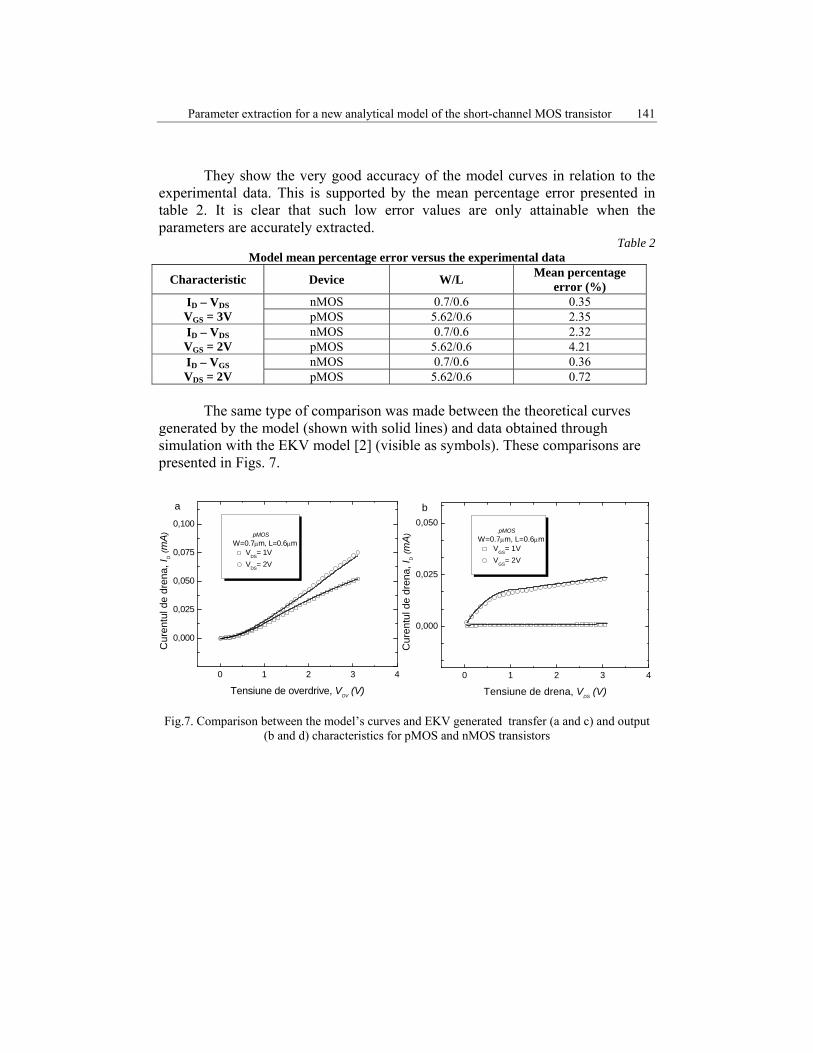
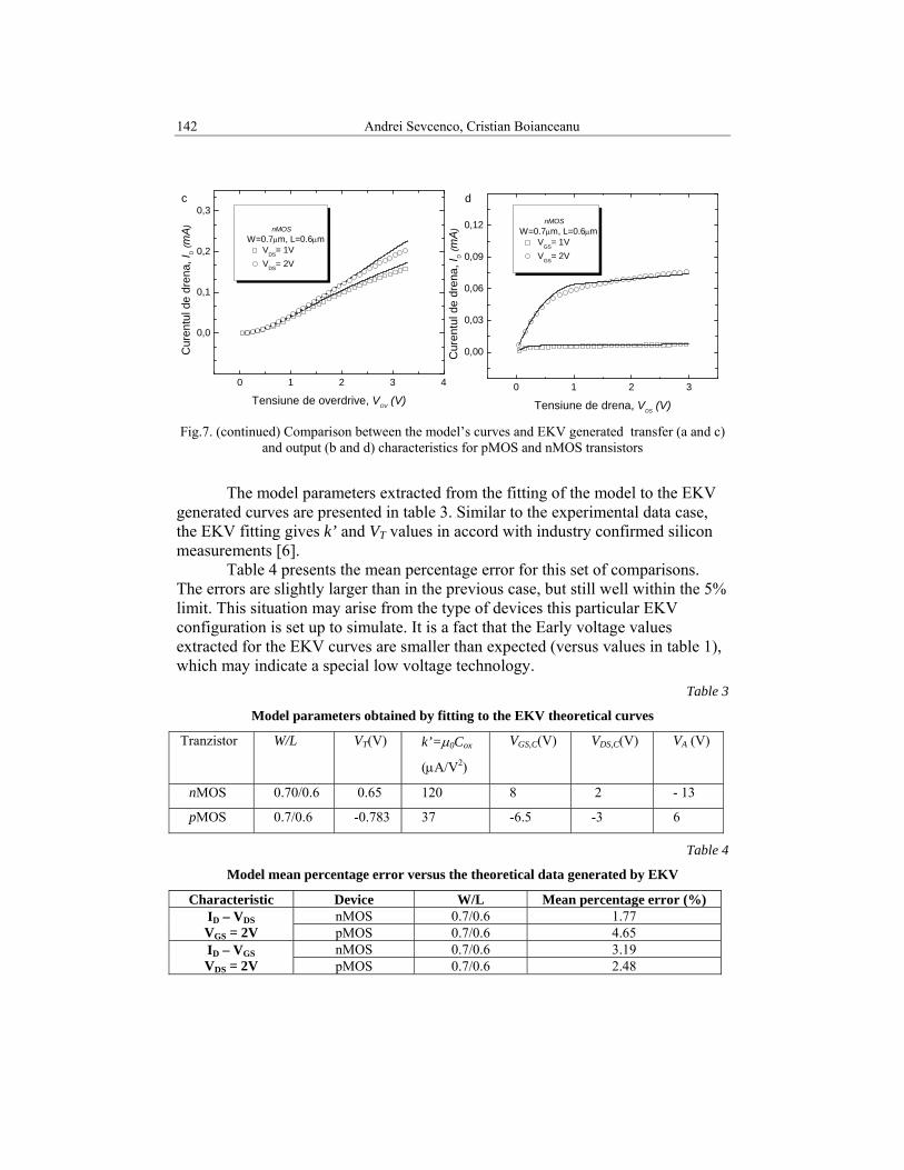
The same type of comparison was made between the theoretical curves
generated by the model (shown with solid lines) and data obtained through simulation with the EKV model [2] (visible as symbols). These comparisons are presented in Figs. 7.
0 1 2 3 4
0,000
0,025
0,050
0,075
0,100
a
pMOSW=0.7μm, L=0.6μm
VDS
= 1V V
DS= 2V
Cur
entu
l de
dren
a, I D
(mA
)
Tensiune de overdrive, VOV
(V)0 1 2 3 4
0,000
0,025
0,050b
pMOSW=0.7μm, L=0.6μm
VGS= 1V VGS= 2V
Cur
entu
l de
dren
a, I D
(mA
)
Tensiune de drena, VDS
(V)
Fig.7. Comparison between the model’s curves and EKV generated transfer (a and c) and output (b and d) characteristics for pMOS and nMOS transistors
142 Andrei Sevcenco, Cristian Boianceanu
0 1 2 3 4
0,0
0,1
0,2
0,3c
nMOSW=0.7μm, L=0.6μm
VDS= 1V VDS= 2V
Cur
entu
l de
dren
a, I D
(mA
)
Tensiune de overdrive, VOV
(V)0 1 2 3
0,00
0,03
0,06
0,09
0,12
d
nMOSW=0.7μm, L=0.6μm
VGS= 1V VGS= 2V
Cur
entu
l de
dren
a, I D
(mA
)
Tensiune de drena, VDS (V) Fig.7. (continued) Comparison between the model’s curves and EKV generated transfer (a and c)
and output (b and d) characteristics for pMOS and nMOS transistors
The model parameters extracted from the fitting of the model to the EKV
generated curves are presented in table 3. Similar to the experimental data case, the EKV fitting gives k’ and VT values in accord with industry confirmed silicon measurements [6].
Table 4 presents the mean percentage error for this set of comparisons. The errors are slightly larger than in the previous case, but still well within the 5% limit. This situation may arise from the type of devices this particular EKV configuration is set up to simulate. It is a fact that the Early voltage values extracted for the EKV curves are smaller than expected (versus values in table 1), which may indicate a special low voltage technology.
Table 3
Model parameters obtained by fitting to the EKV theoretical curves
Tranzistor W/L VT(V) k’=μ0Cox
(μA/V2)
VGS,C(V) VDS,C(V) VA (V)
nMOS 0.70/0.6 0.65 120 8 2 - 13
pMOS 0.7/0.6 -0.783 37 -6.5 -3 6
Table 4
Model mean percentage error versus the theoretical data generated by EKV
Characteristic Device W/L Mean percentage error (%) ID – VDS VGS = 2V
nMOS 0.7/0.6 1.77 pMOS 0.7/0.6 4.65
ID – VGS VDS = 2V
nMOS 0.7/0.6 3.19 pMOS 0.7/0.6 2.48

Parameter extraction for a new analytical model of the short-channel MOS transistor 143
6. Conclusions
This paper presents an original, simple and modular parameter extractor
for a new analytical model for the MOS transistor in analogical applications, which uses five technology parameters. The parameter extractor is built in Labview, using the Levenberg-Marquardt non-linear fitting algorithm.
The extractor, coupled with linear regressions for some of the model parameters, creates a robust and easy to use parameter extraction method, which was used to fit the new MOSFET model to experimental data obtained from measurements made on n and p type MOS transistors with aspect ratios of 5.62/0.6 and 0.7/0.6. The model was also fitted to theoretical curves simulated with the EKV model, for similar aspect ratio devices, using the same extraction method.
The comparisons between the model curves, created with the extracted parameters, and the measured data, as well as simulated data generated by the EKV model, showed the high accuracy of the extraction method used. This is evinced in the low fitting errors attained by the model’s curves when compared to the aforementioned data. This is coupled with the low complexity of the method, showing that it is a valid method for model analysis.
R E F E R E N C E S
[1]. PR. Gray, PJ. Hurst, SH. Lewis, RG. Meyer, “Analysis and Design of Analog IC’s,” Fourth
Ed., J.Whiley&Sons, New York, 2001. [2]. C.C. Enz, F. Krummenacher, E.A. Vittoz, ”An Analytical MOS Transistor Model Valid in
All Regions of Operation and Dedicated to Low-Voltage and Low-Current Applications,” Analog Integrated Circuits and Signal Processing 8 (1995), pp. 83-114.
[3]. G. Brezeanu, A. Sevcenco, ”An accurate model of submicron MOS electrical characteristics for analogue applications,” International Journal of Electronics, vol. 99 (2012), pp. 743-759.
[4]. A. Sevcenco, G. Brezeanu, M. Badila, “A Short Channel MOSFET Modelling for Analog Circuit Design with Emphasis on Carrier Mobility,” Proceedings of the 9th International Symposium on Signals, Circuits, Systems (ISSCS) 2009, 353-356.
[5]. A. Abba, F. Caponio, A. Geraci, G. Ripamonti, ” Implementation of High Efficiency Non-Linear Least-Squares in FPGA Devices for Digital Spectroscopy,” in Proceedings of the Nuclear Science Symposium, 2010, pp. 1371 – 1376.

144 Andrei Sevcenco, Cristian Boianceanu
[6]. MOSIS test data for IBM-Burlington silicon wafers https://www.mosis.com/cgi-bin/cgiwrap/umosis/swp/params/ibm-025
[7]. K.Madsen, H.B.Nielsen, O.Tinglef, “Methods for Non-linear least squares problems”, Informatics and Mathematical Modeling,Technical University of Denmark, 2004.