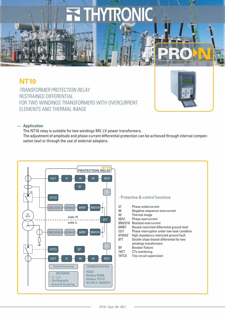
NT10TRANSFORMER PROTECTION RELAY
RESTRAINED DIFFERENTIAL
FOR TWO WINDINGS TRANSFORMERS WITH OVERCURRENT
ELEMENTS AND THERMAL IMAGE
NT10 - Flyer- 09 - 2011
ApplicationThe NT10 relay is suitable for two windings MV, LV power transformers.The adjustment of amplitude and phase current differential protection can be achieved through internal compen-sation (sw) or through the use of external adapters.
—
- Protective & control functions
37 Phase undercurrent46 Negative-sequence overcurrent 49 Thermal image50/51 Phase overcurrent50N/51N Residual overcurrent64REF Biased restricted differential ground faultI2/I1 Phase interruption under low-load condition87NHIZ High impedance restricted ground fault87T Double slope biased differential for two windings transformersBF Breaker Failure74CT CTs monitoring74TCS Trip circuit supervision
74TCS
BF
NT10
side H
side L
50N/51N
52
74TCS BF
87NHIZ50N.1/51N.1
87T
74CT 37 46 49 50/51
74CT 37 46 49 50/51
64REF
50N/51N87NHIZ50N.2/51N.2 64REF
METERING- IL1..IL3,IE
- Oscillography- Events & Faults log
Control functions COMMUNICATION
- RS232- Modbus RS485- Modbus TCP/IP- IEC 870-5-103/DNP3
2 NT10 - Flyer- 09 - 2011
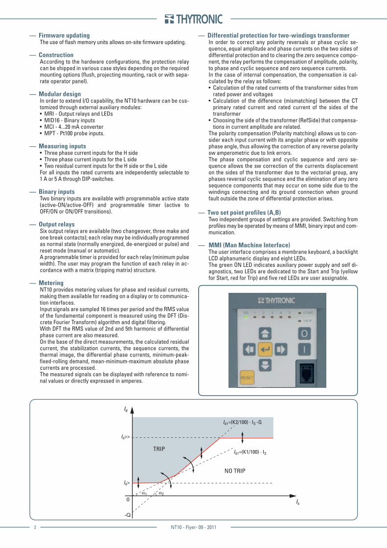
Differential protection for two-windings transformerIn order to correct any polarity reversals or phase cyclic se-quence, equal amplitude and phase currents on the two sides of differential protection and to clearing the zero sequence compo-nent, the relay performs the compensation of amplitude, polarity, to phase and cyclic sequence and zero sequence currents.In the case of internal compensation, the compensation is cal-culated by the relay as follows:
Calculation of the rated currents of the transformer sides from rated power and voltagesCalculation of the difference (mismatching) between the CT primary rated current and rated current of the sides of the transformerChoosing the side of the transformer (RefSide) that compensa-tions in current amplitude are related.
The polarity compensation (Polarity matching) allows us to con-sider each input current with its angular phase or with opposite phase angle, thus allowing the correction of any reverse polarity sw amperometric due to link errors.The phase compensation and cyclic sequence and zero se-quence allows the sw correction of the currents displacement on the sides of the transformer due to the vectorial group, any phases reversal cyclic sequence and the elimination of any zero sequence components that may occur on some side due to the windings connecting and its ground connection when ground fault outside the zone of differential protection arises.
Two set point profiles (A,B)Two independent groups of settings are provided. Switching from profi les may be operated by means of MMI, binary input and com-munication.
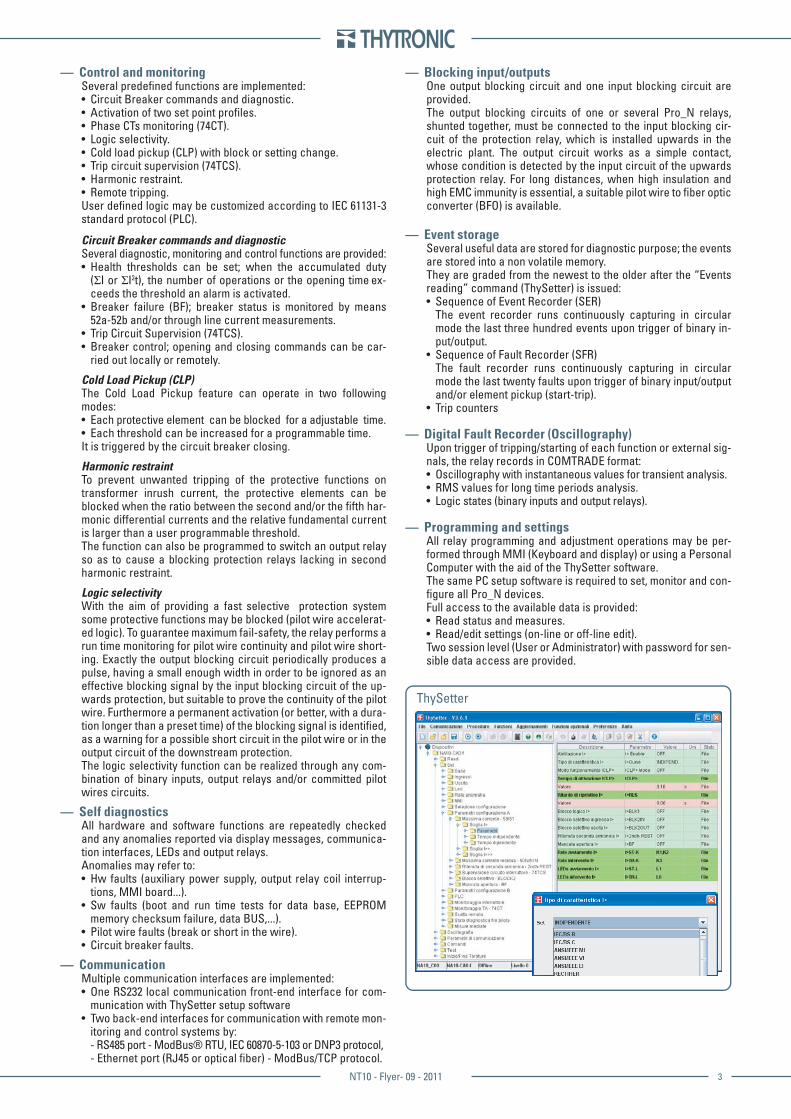
MMI (Man Machine Interface)The user interface comprises a membrane keyboard, a backlight LCD alphanumeric display and eight LEDs.The green ON LED indicates auxiliary power supply and self di-agnostics, two LEDs are dedicated to the Start and Trip (yellow for Start, red for Trip) and fi ve red LEDs are user assignable.
—
•
•
•
—
—
NO TRIP
TRIP
Is
Id
Id>
Id1=(K2/100) ∙ IS -Q
Id1=(K1/100) ∙ IS
0
-Q
α2α1
Id>>
Firmware updatingThe use of fl ash memory units allows on-site fi rmware updating.
ConstructionAccording to the hardware confi gurations, the protection relay can be shipped in various case styles depending on the required mounting options (fl ush, projecting mounting, rack or with sepa-rate operator panel).
Modular designIn order to extend I/O capability, the NT10 hardware can be cus-tomized through external auxiliary modules:
MRI - Output relays and LEDsMID16 - Binary inputsMCI - 4...20 mA converterMPT - Pt100 probe inputs.
Measuring inputsThree phase current inputs for the H sideThree phase current inputs for the L sideTwo residual current inputs for the H side or the L side
For all inputs the rated currents are independently selectable to 1 A or 5 A through DIP-switches.
Binary inputsTwo binary inputs are available with programmable active state (active-ON/active-OFF) and programmable timer (active to OFF/ON or ON/OFF transitions).
Output relaysSix output relays are available (two changeover, three make and one break contacts); each relay may be individually programmed as normal state (normally energized, de-energized or pulse) and reset mode (manual or automatic). A programmable timer is provided for each relay (minimum pulse width). The user may program the function of each relay in ac-cordance with a matrix (tripping matrix) structure.
MeteringNT10 provides metering values for phase and residual currents, making them available for reading on a display or to communica-tion interfaces.Input signals are sampled 16 times per period and the RMS value of the fundamental component is measured using the DFT (Dis-crete Fourier Transform) algorithm and digital fi ltering.With DFT the RMS value of 2nd and 5th harmonic of differential phase current are also measured.On the base of the direct measurements, the calculated residual current, the stabilization currents, the sequence currents, the thermal image, the differential phase currents, minimum-peak-fi xed-rolling demand, mean-minimum-maximum absolute phase currents are processed.The measured signals can be displayed with reference to nomi-nal values or directly expressed in amperes.
—
—
—
••••
—•••
—
—
—
3NT10 - Flyer- 09 - 2011
Control and monitoringSeveral predefi ned functions are implemented:
Circuit Breaker commands and diagnostic.Activation of two set point profi les.Phase CTs monitoring (74CT).Logic selectivity.Cold load pickup (CLP) with block or setting change.Trip circuit supervision (74TCS).Harmonic restraint.Remote tripping.
User defi ned logic may be customized according to IEC 61131-3 standard protocol (PLC).
Circuit Breaker commands and diagnosticSeveral diagnostic, monitoring and control functions are provided:
Health thresholds can be set; when the accumulated duty (ΣI or ΣI2t), the number of operations or the opening time ex-ceeds the threshold an alarm is activated.Breaker failure (BF); breaker status is monitored by means 52a-52b and/or through line current measurements.Trip Circuit Supervision (74TCS).Breaker control; opening and closing commands can be car-ried out locally or remotely.
Cold Load Pickup (CLP)The Cold Load Pickup feature can operate in two following modes:
Each protective element can be blocked for a adjustable time.Each threshold can be increased for a programmable time.
It is triggered by the circuit breaker closing.
Harmonic restraintTo prevent unwanted tripping of the protective functions on transformer inrush current, the protective elements can be blocked when the ratio between the second and/or the fi fth har-monic differential currents and the relative fundamental current is larger than a user programmable threshold.The function can also be programmed to switch an output relay so as to cause a blocking protection relays lacking in second harmonic restraint.
Logic selectivityWith the aim of providing a fast selective protection system some protective functions may be blocked (pilot wire accelerat-ed logic). To guarantee maximum fail-safety, the relay performs a run time monitoring for pilot wire continuity and pilot wire short-ing. Exactly the output blocking circuit periodically produces a pulse, having a small enough width in order to be ignored as an effective blocking signal by the input blocking circuit of the up-wards protection, but suitable to prove the continuity of the pilot wire. Furthermore a permanent activation (or better, with a dura-tion longer than a preset time) of the blocking signal is identifi ed, as a warning for a possible short circuit in the pilot wire or in the output circuit of the downstream protection.The logic selectivity function can be realized through any com-bination of binary inputs, output relays and/or committed pilot wires circuits.
Self diagnosticsAll hardware and software functions are repeatedly checked and any anomalies reported via display messages, communica-tion interfaces, LEDs and output relays. Anomalies may refer to:
Hw faults (auxiliary power supply, output relay coil interrup-tions, MMI board...).Sw faults (boot and run time tests for data base, EEPROM memory checksum failure, data BUS,...).Pilot wire faults (break or short in the wire).Circuit breaker faults.
CommunicationMultiple communication interfaces are implemented:
One RS232 local communication front-end interface for com-munication with ThySetter setup softwareTwo back-end interfaces for communication with remote mon-itoring and control systems by:- RS485 port - ModBus® RTU, IEC 60870-5-103 or DNP3 protocol,- Ethernet port (RJ45 or optical fi ber) - ModBus/TCP protocol.
—
••••••••
•
•
••
••
—
•
•
••
—
•
•
Blocking input/outputsOne output blocking circuit and one input blocking circuit are provided.The output blocking circuits of one or several Pro_N relays, shunted together, must be connected to the input blocking cir-cuit of the protection relay, which is installed upwards in the electric plant. The output circuit works as a simple contact, whose condition is detected by the input circuit of the upwards protection relay. For long distances, when high insulation and high EMC immunity is essential, a suitable pilot wire to fi ber optic converter (BFO) is available.
Event storageSeveral useful data are stored for diagnostic purpose; the events are stored into a non volatile memory.They are graded from the newest to the older after the “Events reading” command (ThySetter) is issued:
Sequence of Event Recorder (SER)The event recorder runs continuously capturing in circular mode the last three hundred events upon trigger of binary in-put/output.Sequence of Fault Recorder (SFR)The fault recorder runs continuously capturing in circular mode the last twenty faults upon trigger of binary input/output and/or element pickup (start-trip).Trip counters
Digital Fault Recorder (Oscillography)Upon trigger of tripping/starting of each function or external sig-nals, the relay records in COMTRADE format:
Oscillography with instantaneous values for transient analysis.RMS values for long time periods analysis.Logic states (binary inputs and output relays).
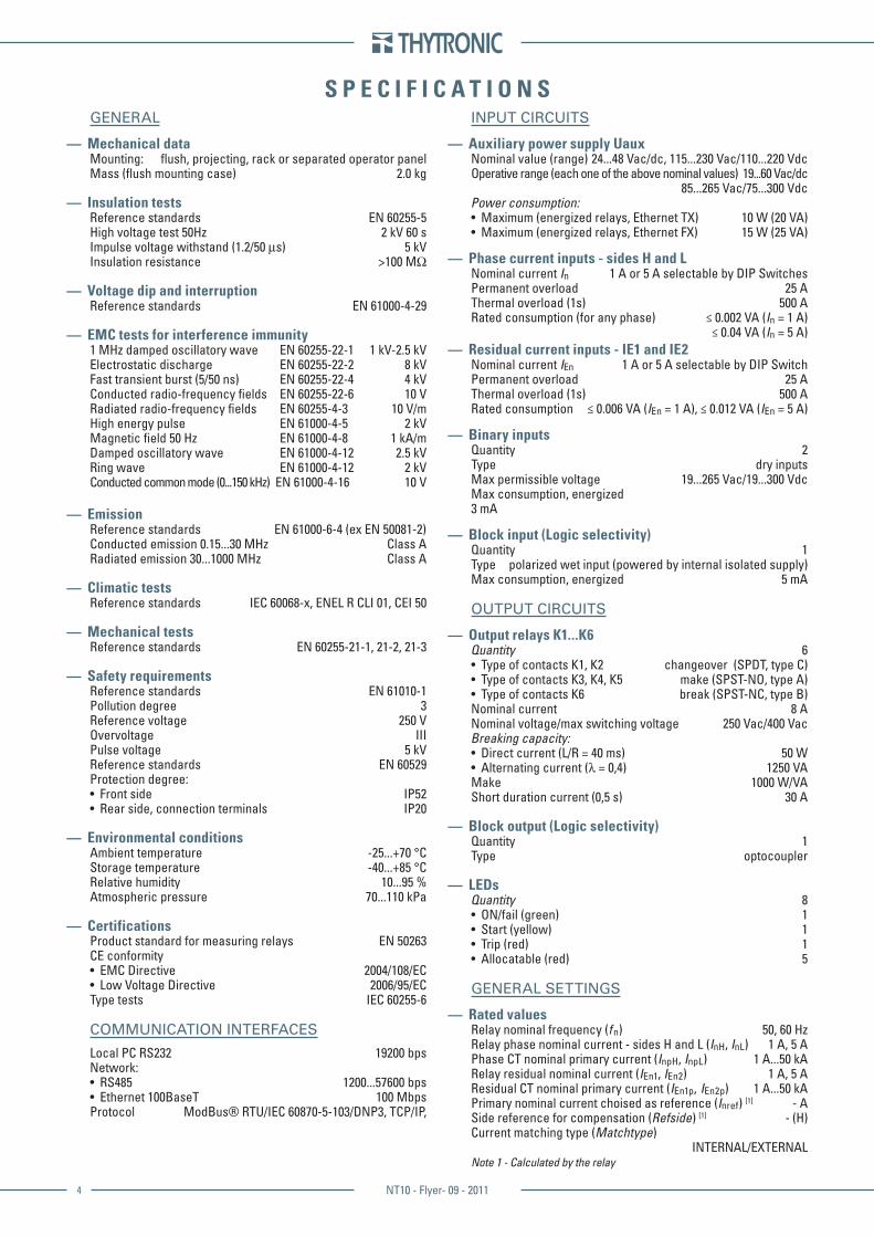
Programming and settingsAll relay programming and adjustment operations may be per-formed through MMI (Keyboard and display) or using a Personal Computer with the aid of the ThySetter software.The same PC setup software is required to set, monitor and con-fi gure all Pro_N devices.Full access to the available data is provided:
Read status and measures.Read/edit settings (on-line or off-line edit).
Two session level (User or Administrator) with password for sen-sible data access are provided.
—
—
•
•
•
—
•••
—
••
ThySetter
4 NT10 - Flyer- 09 - 2011
S P E C I F I C A T I O N SGENERAL
Mechanical dataMounting: fl ush, projecting, rack or separated operator panelMass (fl ush mounting case) 2.0 kg Insulation testsReference standards EN 60255-5High voltage test 50Hz 2 kV 60 sImpulse voltage withstand (1.2/50 μs) 5 kVInsulation resistance >100 MΩ Voltage dip and interruptionReference standards EN 61000-4-29 EMC tests for interference immunity1 MHz damped oscillatory wave EN 60255-22-1 1 kV-2.5 kVElectrostatic discharge EN 60255-22-2 8 kVFast transient burst (5/50 ns) EN 60255-22-4 4 kVConducted radio-frequency fi elds EN 60255-22-6 10 VRadiated radio-frequency fi elds EN 60255-4-3 10 V/mHigh energy pulse EN 61000-4-5 2 kVMagnetic fi eld 50 Hz EN 61000-4-8 1 kA/mDamped oscillatory wave EN 61000-4-12 2.5 kVRing wave EN 61000-4-12 2 kVConducted common mode (0...150 kHz) EN 61000-4-16 10 V
EmissionReference standards EN 61000-6-4 (ex EN 50081-2)Conducted emission 0.15...30 MHz Class ARadiated emission 30...1000 MHz Class A Climatic testsReference standards IEC 60068-x, ENEL R CLI 01, CEI 50 Mechanical testsReference standards EN 60255-21-1, 21-2, 21-3
Safety requirementsReference standards EN 61010-1Pollution degree 3Reference voltage 250 VOvervoltage IIIPulse voltage 5 kVReference standards EN 60529Protection degree:
Front side IP52Rear side, connection terminals IP20
Environmental conditions Ambient temperature -25...+70 °CStorage temperature -40...+85 °CRelative humidity 10...95 %Atmospheric pressure 70...110 kPa
CertificationsProduct standard for measuring relays EN 50263CE conformity
EMC Directive 2004/108/ECLow Voltage Directive 2006/95/EC
Type tests IEC 60255-6
COMMUNICATION INTERFACES
Local PC RS232 19200 bpsNetwork:
RS485 1200...57600 bpsEthernet 100BaseT 100 Mbps
Protocol ModBus® RTU/IEC 60870-5-103/DNP3, TCP/IP,
—
—
—
—
—
—
—
—
••
—
—
••
••
INPUT CIRCUITS
Auxiliary power supply UauxNominal value (range) 24...48 Vac/dc, 115...230 Vac/110...220 VdcOperative range (each one of the above nominal values) 19...60 Vac/dc 85...265 Vac/75...300 VdcPower consumption:
Maximum (energized relays, Ethernet TX) 10 W (20 VA)Maximum (energized relays, Ethernet FX) 15 W (25 VA)
Phase current inputs - sides H and LNominal current In 1 A or 5 A selectable by DIP SwitchesPermanent overload 25 AThermal overload (1s) 500 ARated consumption (for any phase) ≤ 0.002 VA (In = 1 A) ≤ 0.04 VA (In = 5 A)Residual current inputs - IE1 and IE2Nominal current IEn 1 A or 5 A selectable by DIP SwitchPermanent overload 25 AThermal overload (1s) 500 ARated consumption ≤ 0.006 VA (IEn = 1 A), ≤ 0.012 VA (IEn = 5 A)
Binary inputsQuantity 2 Type dry inputsMax permissible voltage 19...265 Vac/19...300 VdcMax consumption, energized 3 mA
Block input (Logic selectivity)Quantity 1Type polarized wet input (powered by internal isolated supply) Max consumption, energized 5 mA
OUTPUT CIRCUITS
Output relays K1...K6 Quantity 6
Type of contacts K1, K2 changeover (SPDT, type C) Type of contacts K3, K4, K5 make (SPST-NO, type A)Type of contacts K6 break (SPST-NC, type B)
Nominal current 8 ANominal voltage/max switching voltage 250 Vac/400 VacBreaking capacity:
Direct current (L/R = 40 ms) 50 WAlternating current (λ = 0,4) 1250 VA
Make 1000 W/VAShort duration current (0,5 s) 30 A Block output (Logic selectivity)Quantity 1Type optocoupler
LEDsQuantity 8
ON/fail (green) 1Start (yellow) 1Trip (red) 1Allocatable (red) 5
GENERAL SETTINGS
Rated valuesRelay nominal frequency (f n) 50, 60 HzRelay phase nominal current - sides H and L (InH, InL) 1 A, 5 APhase CT nominal primary current (InpH, InpL) 1 A...50 kARelay residual nominal current (IEn1, IEn2) 1 A, 5 AResidual CT nominal primary current (IEn1p, IEn2p) 1 A...50 kAPrimary nominal current choised as reference (Inref) [1] - ASide reference for compensation (Refside) [1] - (H)Current matching type (Matchtype) INTERNAL/EXTERNALNote 1 - Calculated by the relay
—
••
—
—
—
—
—
•••
••
—
—
••••
—
5NT10 - Flyer- 09 - 2011
Transformer dataTransformer nominal power (Snt) 0.01...1000 MVATransformer nominal voltage side H (VntH) 0.200...500 kVTransformer nominal current side H (IntH) [1] -Transformer mismatching factor side H (mH) [1] -Transformer base current side H (IBH) [1] - InHTransformer grounding side H (GndH) In/OutTransformer connection side H (ConnH) Y/D/ZTransformer vector group side H (VectGroupH) 0Transformer nominal voltage side L (VntL) 0.200...500 kVTransformer nominal current side L (IntL) [1] -Transformer mismatching factor side L (mL) [1] -Transformer base current side L (IBL) [1] - InLTransformer grounding side L (GndL) In/OutTransformer connection side L (ConnL) y/d/zTransformer vector group side L (VectGroupL) 0-1-2...11
Note 1 - Calculated by the relay
Binary input timersON delay time (IN1 tON, IN2 tON,...IN5 tON) 0.00...100.0 sOFF delay time (IN1 tOFF, IN2 tOFF,...IN5 tOFF) 0.00...100.0 sLogic Active-ON/Active-OFF
Relay output timersMinimum pulse width (tTR) 0.000...0.500 s
Input sequencePhase current sequence side H (I-SequenceH) IL1-IL2-IL3, IL1-IL3-IL2....Phase current sequence side L (I-SequenceL) IL1-IL2-IL3, IL1-IL3-IL2....PolarityC09-C10 (IL1H) NORMAL/REVERSEC11-C12 (IL21H) NORMAL/REVERSEC...- C... (I..) NORMAL/REVERSEC07-C08 (IE2) NORMAL/REVERSE
PROTECTIVE FUNCTIONS
Thermal protection with RTD thermometric probes - 26Alarm
Alarm threshold θALx (x=1...8) 0...200 °COperating time tθALx (x=1...8) 0....100 s
TripTrip threshold θ>x (x=1...8) 0...200 °COperating time tθ>x (x=1...8) 0....100 s
Note: The element becomes available when the MPT module is enabled and connected to Thybus
Undercurrent - 37 side HIH< Element
37 Operating logic (Logic37H) AND/OR37 First threshold defi nite time (IH<def) 0.10...1.00 InHIH< Operating time (tIH<def) 0.04...200 s
Undercurrent - 37 side LIL< Element
37 Operating logic (Logic37L) AND/OR37 First threshold defi nite time (IL<def) 0.10...1.00 InLIL< Operating time (tIL<def) 0.04...200 s
Negative sequence - 46 side HI2H> Element
I2H> Curve type DEFINITE IEC/BS A, B, C - ANSI/IEEE MI, VI, EI, I2t or EM
I2HCLP> Activation time (t2HCLP>) 0.00...100.0 sI2H> Reset time delay (t2H>RES) 0.00...100.0 s
Defi nite time46 First threshold defi nite time (I2H>def) 0.100...10.00 InHI2H>def within CLP (I2HCLP>def) 0.100...10.00 InHI2H>def Operating time (t2H>def) 0.03...200 s
Inverse time46 First threshold inverse time (I2H>inv) 0.100...10.00 InHI2H>inv within CLP (I2HCLP>inv) 0.100...10.00 InHI2H>inv Operating time (t2H>inv) 0.02...60.0 s
—
—
—
—
—
—
••
••
—
•••
—
•••
—
•
••
•••
•••
I2H>> ElementI2HCLP>> Activation time (t2HCLP>>) 0.00...100.0 sI2H>> Reset time delay (t2H>>RES) 0.00...100.0 s
Defi nite time46 Second threshold defi nite time (I2H>>def) 0.100...40.00 InHI2H>>def within CLP (I2HCLP>>def) 0.100...40.00 InHI2H>>def Operating time (t2H>>def) 0.03...10.00 s
Negative sequence - 46 side LI2L> Element
I2L> Curve type DEFINITE IEC/BS A, B, C - ANSI/IEEE MI, VI, EI, I2t or EM
I2LCLP> Activation time (t2LCLP>) 0.00...100.0 sI2L> Reset time delay (t2L>RES) 0.00...100.0 s
Defi nite time46 First threshold defi nite time (I2L>def) 0.100...10.00 InLI2L>def within CLP (I2LCLP>def) 0.100...10.00 InLI2L>def Operating time (t2L>def) 0.03...200 s
Inverse time46 First threshold inverse time (I2L>inv) 0.100...10.00 InLI2L>inv within CLP (I2LCLP>inv) 0.100...10.00 InLI2L>inv Operating time (t2L>inv) 0.02...60.0 s
I2L>> ElementI2LCLP>> Activation time (t2LCLP>>) 0.00...100.0 sI2L>> Reset time delay (t2L>>RES) 0.00...100.0 s
Defi nite time46 Second threshold defi nite time (I2L>>def) 0.100...40.00 InLI2L>>def within CLP (I2LCLP>>def) 0.100...40.00 InLI2L>>def Operating time (t2L>>def) 0.03...10.00 s
Negative sequence current / positive sequence current ratio - I2/I1 side H(I2H/I1H)> Element
(I2H/I1H)CLP> Activation time (t 21HCLP>) 0.00...100.0 sDefi nite time
I2H/I1H First threshold defi nite time (I21H>def) 0.10...1.00(I2H/I1H)>def within CLP (I21HCLP>) 0.10...1.00(I2H/I1H)> Operating time (t 21H>def) 0.04...15000 s
Negative sequence current / positive sequence current ratio - I2/I1 side L(I2L/I1L)> Element
(I2L/I1L)CLP> Activation time (t 21LCLP>) 0.00...100.0 sDefi nite time
I2L/I1L First threshold defi nite time (I21L>def) 0.10...1.00(I2L/I1L)>def within CLP (I21LCLP>) 0.10...1.00(I2H/I1H)> Operating time (t 21H>def) 0.04...15000 s
Thermal image - 49 side HCommon confi guration:
Initial thermal image ΔθINH (DthINH) 0.0...1.0 ΔθBHReduction factor at inrush (KINRH) 1.0...3.0Thermal time constant τ (TH) 1...200 minDthCLPH Activation time (tDthCLPH) 0.00...100.0 s
DtHAL1H Element49 First alarm threshold ΔθAL1H (DthAL1H) 0.3...1.0 ΔθBH
DtHAL2H Element49 Second alarm threshold ΔθAL2H (DthAL2H) 0.5...1.2 ΔθBH
Dth> Element49 Trip threshold ΔθH (DthH>) 1.100...1.300 ΔθBH
Thermal image - 49 side LCommon confi guration:
Initial thermal image ΔθINL (DthINL) 0.0...1.0 ΔθBLReduction factor at inrush (KINRL) 1.0...3.0Thermal time constant τ (TL) 1...200 minDthCLPH Activation time (tDthCLPL) 0.00...100.0 s
DtHAL1L Element49 First alarm threshold ΔθAL1L (DthAL1L) 0.3...1.0 ΔθBLDtHAL2L Element49 Second alarm threshold ΔθAL2L (DthAL2L) 0.5...1.2 ΔθBLDth> Element49 Trip threshold ΔθL (DthL>) 1.100...1.300 ΔθBL
••
•••
—
•
••
•••
•••
••
•••
—
•
•••
—
•
•••
—
••••
•
•
•
—
••••
•••••
6 NT10 - Flyer- 09 - 2011
Phase overcurrent - 50/51 side H IH> Element
IH> Curve type (IH>Curve) DEFINITE IEC/BS A, B, C, ANSI/IEEE MI, VI, EI, RECTIFIER, I2t or EM
IHCLP> Activation time (tHCLP>) 0.00...100.0 sIH> Reset time delay (tH>RES) 0.00...100.0 s
Defi nite time50/51 First threshold defi nite time (IH>def) 0.100...40.0 InHIH>def within CLP (IHCLP>def) 0.100...40.0 InHIH>def Operating time (tH>def) 0.04...200 s
Inverse time50/51 First threshold inverse timee (IH>inv) 0.100...20.00 InHIH>inv within CLP (IHCLP>inv) 0.100...20.00 InHIH>inv Operating time (tH>inv) 0.02...60.0 s
IH>> ElementIH>> Type characteristic (IH>>Curve) DEFINITE, I2tIHCLP>> Activation time (tHCLP>>) 0.00...100.0 sIH>> Reset time delay (tH>>RES) 0.00...100.0 s
Defi nite time50/51 Second threshold defi nite time (IH>>def) 0.100...40.0 InHIH>>def within CLP (IHCLP>>def) 0.100...40.0 InHIH>>def Operating time (tH>>def) 0.03...10.00 s
Inverse time50/51 Second threshold inverse time (IH>>inv) 0.100...20.00 InHIH>>inv within CLP (IHCLP>>inv) 0.100...20.00 InHIH>>inv Operating time (tH>>inv) 0.02...10.00 s
IH>>> ElementIHCLP>>> Activation time (tHCLP>>>) 0.00...100.0 sIH>>> Reset time delay (tH>>>RES) 0.00...100.0 s
Defi nite time50/51 Third threshold defi nite time (IH>>>def) 0.100...40.0 InHIH>>>def within CLP (IHCLP>>>def) 0.100...40.0 InHIH>>>def Operating time (tH>>>def) 0.03...10.00 s
Phase overcurrent - 50/51 side L IL> Element
IL> Curve type (IL>Curve) DEFINITE IEC/BS A, B, C, ANSI/IEEE MI, VI, EI, RECTIFIER, I2t or EM
ILCLP> Activation time (tLCLP>) 0.00...100.0 sIL> Reset time delay (tL>RES) 0.00...100.0 s
Defi nite time50/51 First threshold defi nite time (IL>def) 0.100...40.0 InLIHL>def within CLP (ILCLP>def) 0.100...40.0 InLIL>def Operating time (tL>def) 0.04...200 s
Inverse time50/51 First threshold inverse time (IL>inv) 0.100...20.00 InLIL>inv within CLP (IHCLP>inv) 0.100...20.00 InLIL>inv Operating time (tL>inv) 0.02...60.0 s
IL>> ElementIL>> Type characteristic (IL>>Curve) DEFINITE, I2tIHLCLP>> Activation time (tLCLP>>) 0.00...100.0 sIL>> Reset time delay (tL>>RES) 0.00...100.0 s
Defi nite time50/51 Second threshold defi nite time (IL>>def) 0.100...40.0 InLIL>>def within CLP (ILCLP>>def) 0.100...40.0 InLIL>>def Operating time (tL>>def) 0.03...10.00 s
Inverse time50/51 Second threshold inverse time (IL>>inv) 0.100...20.00 InLIL>>inv within CLP (ILCLP>>inv) 0.100...20.00 InLIL>>inv Operating time (tL>>inv) 0.02...10.00 s
IL>>> ElementILCLP>>> Activation time (tLCLP>>>) 0.00...100.0 sIL>>> Reset time delay (tL>>>RES) 0.00...100.0 s
Defi nite time50/51 Third threshold defi nite time (IL>>>def) 0.100...40.0 InLIL>>>def within CLP (ILCLP>>>def) 0.100...40.0 InLIL>>>def Operating time (tL>>>def) 0.03...10.00 s
—
•
••
•••
•••
•••
•••
•••
••
•••
—
•
••
•••
•••
•••
•••
•••
••
•••
Computed residual overcurrent - 50N/51N side HIEH> Element
IEH> Type characteristic (IEH>Curve) DEFINITE IEC/BS A, B, C, ANSI/IEEE MI, VI, EI, EM
IEHCLP> Activation time (tECLP>) 0.00...100.0 sIEH> Reset time delay (tEH>RES) 0.00...100.0 s
Defi nite time50N/51N First threshold defi nite time (IEH>def) 0.002...10.00 InHIEH>def within CLP (IEHCLP>def) 0.002...10.00 InHIEH>def Operating time (tEH>def) 0.04...200 s
Inverse time50N/51N First threshold inverse time (IEH>inv) 0.002...2.00 InHIE>inv within CLP (IEHCLP>inv) 0.002...2.00 InHIE>inv Operating time (tEH>inv) 0.02...60.0 s
IEH>> ElementIEHCLP>> Activation time (tEHCLP>>) 0.00...100.0 sIEH>> Reset time delay (tEH>>RES) 0.00...100.0 s
Defi nite time50N/51N Second threshold inverse time (IEH>>def) 0.002...10.00 InHIEH>>def within CLP (IEHCLP>>def) 0.002...10.00 InHIE>>def Operating time (tE>>def) 0.03...10.00 s
IEH>>> ElementIEHCLP>>> Activation time (tEHCLP>>>) 0.00...100.0 sIEH>>> Reset time delay (tEH>>>RES) 0.00...100.0 s
Defi nite time50N/51N Third threshold defi nite time (IEH>>>def) 0.002...10.00 InHIEHCLP>>>def within CLP (IEHCLP>>>def) 0.002...10.00 InHIEH>>>def Operating time (tEH>>>def) 0.03...10.00 s
Computed residual overcurrent - 50N/51N side LIEL> Element
IEL> Curve type (IEL>Curve) DEFINITE IEC/BS A, B, C, ANSI/IEEE MI, VI, EI, EM
IELCLP> Activation time (tECLP>) 0.00...100.0 sIEL> Reset time delay (tEL>RES) 0.00...100.0 s
Defi nite time50N/51N First threshold defi nite time (IEL>def) 0.002...10.00 InLIEL>def within CLP (IELCLP>def) 0.002...10.00 InLIEL>def Operating time (tEL>def) 0.04...200 s
Inverse time50N/51N First threshold inverse time (IEL>inv) 0.002...2.00 InLIE>inv within CLP (IELCLP>inv) 0.002...2.00 InLIE>inv Operating time (tEL>inv) 0.02...60.0 s
IEL>> ElementIELCLP>> Activation time (tELCLP>>) 0.00...100.0 sIEL>> Reset time delay (tEL>>RES) 0.00...100.0 s
Defi nite time50N/51N Second threshold inverse time (IEL>>def) 0.002...10.00 InLIEL>>def within CLP (IELCLP>>def) 0.002...10.00 InLIE>>def Operating time (tE>>def) 0.03...10.00 s
IEL>>> Element
IELCLP>>> Activation time (tELCLP>>>) 0.00...100.0 sIELCLP>>> Reset time delay (tEL>>>RES) 0.00...100.0 s
Defi nite time50N/51N Third threshold defi nite time (IEL>>>def) 0.002...10.00 InLELCLP>>>def within CLP (IELCLP>>>def) 0.002...10.00 InLIEL>>>def Operating time (tEL>>>def) 0.03...10.00 s
Measured residual overcurrent IE1 - 50N/51NIE1> Element
IE1> Curve type (IE1>Curve) INDIPENDENTE IEC/BS A, B, C, ANSI/IEEE MI, VI, EI, EM
IE1CLP> Activation time (tE1CLP>) 0.00...100.0 sIE1> Reset time delay (tE1>RES) 0.00...100.0 s
Defi nite time50N/51N First threshold defi nite time (IE1>def) 0.002...10.00 IEn1IE1>def within CLP (IE1CLP>def) 0.002...10.00 IEn1IE1>def Operating time (tE1>def) 0.04...200 s
Inverse time50N/51N First threshold inverse time (IE1>inv) 0.002...2.00 IEn1IE1>inv within CLP (IE1CLP>inv) 0.002...2.00 IEn1IE1>inv Operating time (tE1>inv) 0.02...60.0 s
—
•
••
•••
•••
••
•••
••
•••
—
•
••
•••
•••
••
•••
••
•••
—
•
••
•••
•••
7NT10 - Flyer- 09 - 2011
IE1>> ElementIE1CLP>> Activation time (tE1CLP>>) 0.00...100.0 sIE1>> Reset time delay (tE1>>RES) 0.00...100.0 s
Defi nite time50N/51N Second threshold inverse time (IE1>>def) 0.002...10.00 IEn1IE1>>def within CLP (IE1CLP>>def) 0.002...10.00 IEn1IE1>>def Operating time (tE1>>def) 0.03...10.00 s
IE1>>> Element
IE1CLP>>> Activation time (tE1CLP>>>) 0.00...100.0 sIE1CLP>>> Reset time delay (tE1>>>RES) 0.00...100.0 s
Defi nite time50N/51N Third threshold defi nite time (IE1>>>def) 0.002...10.00 IEn1IE1CLP>>>def within CLP (IE1CLP>>>def) 0.002...10.00 IEn1IE1>>>def Operating time (tE1>>>def) 0.03...10.00 s
Measured residual overcurrent IE2 - 50N/51NIE2> Element
IE2> Curve type (IE1>Curve) INDIPENDENTE IEC/BS A, B, C, ANSI/IEEE MI, VI, EI, EM
IE2CLP> Activation time (tE1CLP>) 0.00...100.0 sIE2> Reset time delay (tE1>RES) 0.00...100.0 s
Defi nite time50N/51N First threshold defi nite time (IE1>def) 0.002...10.00 IEn2IE2>def within CLP (IE2CLP>def) 0.002...10.00 IEn2IE2>def Operating time (tE2>def) 0.04...200 s
Inverse time50N/51N First threshold inverse time (IE2>inv) 0.002...2.00 IEn2IE2>inv within CLP (IE2CLP>inv) 0.002...2.00 IEn2IE2>inv Operating time (tE2>inv) 0.02...60.0 s
IE2>> ElementIE2CLP>> Activation time (tE2CLP>>) 0.00...100.0 sIE2>> Reset time delay (tE2>>RES) 0.00...100.0 s
Defi nite time50N/51N Second threshold inverse time (IE2>>def) 0.002...10.00 IEn2IE2>>def within CLP (IE2CLP>>def) 0.002...10.00 IEn2IE2>>def Operating time (tE2>>def) 0.03...10.00 s
IE2>>> Element
IE1CLP>>> Activation time (tE2CLP>>>) 0.00...100.0 sIE2CLP>>> Reset time delay (tE2>>>RES) 0.00...100.0 s
Defi nite time50N/51N Third threshold defi nite time (IE2>>>def) 0.002...10.00 IEn2IE2CLP>>>def within CLP (IE2CLP>>>def) 0.002...10.00 IEn2IE2>>>def Operating time (tE2>>>def) 0.03...10.00 s
Low impedance restricted ground fault - 64REF side H64REF Minimum threshold (IREFH>) 0.05...2.00 IEn164REF Intentional delay (tREFH>) 0.03...60.00 s
Low impedance restricted ground fault - 64REF side L64REF Minimum threshold (IREFL>) 0.05...2.00 IEn264REF Intentional delay (tREFL>) 0.03...60.00 s
Differential for two windings transformer - 87THarmonic restraint:
2nd harmonic restraint (2nd-REST>) 10...80% Id5th harmonic restraint (5th-REST>) 10...80% IdRestraint reset intentional delay (tHREST-RES) 0.00...10.00 sCross-harmonic restraint enabling (CROSS H-RES) ON/OFFCT saturation detector87T Saturation detector enable (Sat-Det) ON/OFF87T Saturation detector reset intentional delay (tSat-Det-RES) 0.00...0.50 sId> Element Defi nite time87 First threshold defi nite time (Id>) 0.05...2.00 Inref87T First stretch slope percentage (K1) 10...50%87T Second stretch slope percentage (K2) 25...100% 87T Second stretch Intersection with vertical axis (Q) 0.00...3.00 Inref 87T First threshold operating time 0.04 s
Id>> Element Defi nite time87T Second threshold defi nite time (Id>>) 0.5...30.00 Inref87T Second threshold operating time 0.03 s
••
•••
••
•••
—
•
••
•••
•••
••
•••
••
•••
—••
—••
—
•••••••
••••••
••
Breaker failure - BF side HBF Phase current threshold (IBFH>) 0.05...1.00 InHBF Residual current threshold (IEBFH>) 0.01..2.00 InHBF Time delay (tBFH) 0.06...10.00 s
Breaker failure - BF side LBF Phase current threshold (IBFL>) 0.05...1.00 InLBF Residual current threshold (IEBFL>) 0.01..2.00 InLBF Time delay (tBFL) 0.06...10.00 s
Selective block - BLOCK2Selective block IN:
BLIN Max activation time for phase protections (tBH-Iph) 0.10...10.00 sBLIN Max activation time for earth protections (tBH-IE) 0.10...10.00 s
Selective block OUT:BLOUT Dropout time delay for phase protections (tFH-Iph) 0.00...1.00 sBLOUT Drop-out time delay for ground protections (tFH-IE) 0.00...1.00 sBLOUT Drop-out time delay for phase and ground protections (tFH-Iph/IE) 0.00...1.00 s
Internal selective block - BLOCK4Output selective block dropout time for phase protections (tF-IPh) 0.00...10.00 sOutput selective block dropout time for ground protections (tF-IE) 0.00...10.00 sCT supervision - 74CT side H74CT Threshold (SH<) 0.10...0.9574CT Overcurrent threshold (IH*) 0.10...1.00 InHSH< Operate time (tSH) 0.03...200 s
CT supervision - 74CT side L74CT Threshold (SL<) 0.10...0.9574CT Overcurrent threshold (IL*) 0.10...1.00 InHSL< Operate time (tSL) 0.03...200 s
Circuit Breaker supervision side HNumber of CB trips (N.OpenH) 0...10000Cumulative CB tripping currents (SumIH) 0...5000 InHCB opening time for I^2t calculation ΣI2t (tbreakH) 0.05...1.00 sCumulative CB tripping I^2t (SumI^2tH) 0...5000 InH2.sCB max allowed opening time (tbreakH>) 0.05...1.00 s
Circuit Breaker supervision side LNumber of CB trips (N.OpenL) 0...10000Cumulative CB tripping currents (SumIL) 0...5000 InLCB opening time for I^2t calculation ΣI2t (tbreakL) 0.05...1.00 sCumulative CB tripping I^2t (SumI^2tL) 0...5000 InL2.sCB max allowed opening time (tbreakL>) 0.05...1.00 s
Pilot wire diagnosticBLOUT1 Diagnostic pulses period (PulseBLOUT1) OFF - 0.1-1-5-10-60-120 sBLIN1 Diagnostic pulses control time interval (PulseBLIN1) OFF - 0.1-1-5-10-60-120 s
—
—
—
•
•
•••
—
—
—
—
—
—
8 NT10 - Flyer- 09 - 2011
METERING & RECORDING
Measured parametersDirect:
Frequency fFundamental RMS phase currents side H IL1H, IL2H, IL3H Fundamental RMS phase currents side L IL1L, IL2L, IL3L Fundamental RMS residual currents (measured) IE1, IE2
Calculated:Calculated residual current side H and L IEH, IEL Thermal image side H and L DThH, DThL Maximum current between IL1-IL2-IL3 side H and L ILmaxH, ILmaxLMinimum current between IL1-IL2-IL3 side H and L ILminH, ILminLAverage current between IL1-IL2-IL3 side H and L ILH, ILLCompensated phase currents side H IL1cH, IL2cH, IL3cH Compensated phase currents side L IL1cL, IL2cL, IL3cL Stabilization currents (87 element) ISL1, ISL2, ISL3 Differential currents IdL1, IdL2, IdL3Stabilization current (64REF-1 element) side H IESHStabilization current (64REF-2 element) side L IESL
Sequence:Positive sequence current side H and L I1H, I1LNegative sequence current side H and L I2H, I2LMaximum of the second harmonic phase currents/fundamental component percentage ratio side H and L I-2nd /IL I2H/I1H, I2L/I1L
2nd harmonic:Second harmonic differential currents Id2L1, Id2L2, Id2L3
5th harmonic:Fifth harmonic differential currents Id5L1, Id5L2, Id5L3
On demand:Phase fi xed currents demand side H IL1FIXH, IL2FIXH, IL3FIXHPhase rolling currents demand side H IL1ROLH, IL2ROLH, IL3ROLHPhase peak currents demand side HIL1MA XH, IL2MA XH, IL3MA XHPhase minimum currents demand side H IL1MINH, IL2MINH, IL3MINHPhase fi xed currents demand side L IL1FIXL, IL2FIXL, IL3FIXLPhase rolling currents demand side L IL1ROLL, IL2ROLL, IL3ROLLPhase peak currents demand side L IL1MA XL, IL2MA XL, IL3MA XLPhase minimum currents demand side L IL1MINL, IL2MINL, IL3MINL
Event recording (SER)Number of events 300 Recording mode circularTrigger:
Start and trip of any enabled protection or control functionBinary inputs switching (off/on and on/off)Power ON and power OFF (auxiliary power supply)Setting changes
Data recorded: Event counter (resettable by ThySetter) 0...109
Event cause binary input/output relay/setting changesTime stamp Date and time
Fault recording (SFR)Number of faults 20Recording mode circularTrigger:
External trigger binary input set as Fault triggerElement and control pickup output relays OFF-ON transition
Data recorded:Time stamp Date and timeFault cause start, trip, binary inputFault counter (resettable by ThySetter) 0...109
Phase currents side H and side L IL1Hr, IL2Hr, IL3Hr, IL1Lr, IL2Lr, IL3LrMeasured residual currents IE1r, IE2rDifferential currents IdL1r, IdL2r, IdL3r2nd harmonic of differential currents Id2L1r, Id2L2r, Id2L3r5th harmonic of differential currents Id5L1r, Id5L2r, Id5L3rThermal image side H and side L DThetaH-r, DThetaH-rBinary inputs state IN1, IN2...INxOutput relays state K1...K6...K10Fault cause info (operating phase) L1, L2, L3
—
••••
•••••••••••
•••
•
•
••••••••
—
••••
•••
—
••
••••••••••••
Digital Fault Recorder (Oscillography)File format COMTRADERecords depending on setting [1]
Recording mode circularSampling rate 16 sample/cycleTrigger setup:
Pre-trigger time 0.05...1.00 sPost-trigger time 0.05...60.00 sTrigger from inputs IN1, IN2...INxTrigger from outputs K1...K6...K10Communication ThySetter
Set sample channels: Instantaneous phase currents side H iL1H, iL2H, iL3HInstantaneous phase currents side L iL1L, iL2L, iL3LCompensated phase currents side H iL1cH, iL2cH, iL3cH Compensated phase currents side L iL1cL, iL2cL, iL3cLStabilization currents (87 element) iSL1, iSL2, iSL3 Differential currents idL1, idL2, idL3Instantaneous measured residual currents iE1, iE2
Set analog channels (Analog 1...12): Frequency fFundamental RMS phase currents side H IL1H, IL2H, IL3H Fundamental RMS phase currents s side L IL1L, IL2L, IL3L Thermal image side H and side L DThH, DThL Fundamental RMS residual currents (measured) IE1, IE2Fundamental RMS residual currents (computed) side H and L IEH, IEL Compensated phase currents side H IL1cH, IL2cH, IL3cH Compensated phase currents side L IL1cL, IL2cL, IL3cLStabilization currents (87 element) ISL1, ISL2, ISL3 Differential currents IdL1, IdL2, IdL3Second harmonic differential currents Id2L1, Id2L2, Id2L3Fifth harmonic differential currents Id5L1, Id5L2, Id5L3Stabilization current (64REF-1 element) side H IESHStabilization current (64REF-2 element) side L IESLFundamental RMS positive sequence currents side H and L I1H, I1LFundamental RMS negative sequence currents side H and L I2H, I2LMaximum of the second harmonic phase currents/fundamental component percentage ratio side H and L I-2nd /IL I2H/I1H, I2L/I1LTemperature T1...T8
Set digital channels (Digital 1...12): Output relays state K1...K6...K10Binary inputs state IN1, IN2...INx
Note [1] - For instance, with following setting:Pre-trigger time and Post-trigger time 0.25 sSampled channels iL1H, iL2H, iL3H, iL1L, iL2L, iL3L, idL1, idL2, idL3, iE1, iE2Analog channels IL1H, IL2H, IL3H, IL1L, IL2L, IL3L, IdL1, IdL2, IdL3, IE1, IE2Digital channels K1, K2, K3, K4, K5, K6, IN1, IN2
up to 200 records can be stored with f = 50 Hz
—
•••••
•••••••
•••••••••••••••••
•
••
••••
9NT10 - Flyer- 09 - 2011
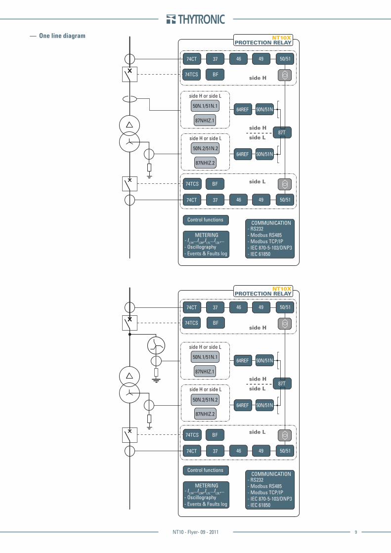
One line diagram—
74TCS BF
NT10X
side H
side H
side L
side L
50N/51N
74TCS BF
METERING- IL1H...IL3H,IL1L...IL3L,...- Oscillography- Events & Faults log
COMMUNICATION- RS232- Modbus RS485- Modbus TCP/IP- IEC 870-5-103/DNP3- IEC 61850
87T
74CT 37 46 49 50/51
74CT 37 46 49 50/51
64REF
50N/51N64REF
87NHIZ.2
side H or side L
50N.1/51N.1
50N.2/51N.2
87NHIZ.1
side H or side L
74TCS BF
NT10X
side H
side H
side L
side L
50N/51N
74TCS BF
METERING- IL1H...IL3H,IL1L...IL3L,...- Oscillography- Events & Faults log
COMMUNICATION- RS232- Modbus RS485- Modbus TCP/IP- IEC 870-5-103/DNP3- IEC 61850
87T
74CT 37 46 49 50/51
74CT 37 46 49 50/51
64REF
50N/51N64REF50N.2/51N.2
87NHIZ.2
side H or side L
50N.1/51N.1
87NHIZ.1
side H or side L
Control functions
Control functions
10 NT10 - Flyer- 09 - 2011
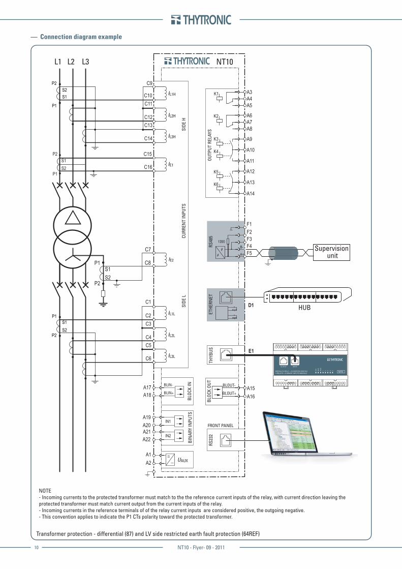
Transformer protection - differential (87) and LV side restricted earth fault protection (64REF)
NOTE- Incoming currents to the protected transformer must match to the the reference current inputs of the relay, with current direction leaving the protected transformer must match current output from the current inputs of the relay.- Incoming currents in the reference terminals of of the relay current inputs are considered positive, the outgoing negative.- This convention applies to indicate the P1 CTs polarity toward the protected transformer.
NT10
E1
THYB
US
D1
ETHE
RNET
HUB
RS23
2
FRONT PANEL
OUTPUT
ON
BU
S
RU
N
1 2 3 4 5MODULO 4 RELE’ + 8 INGRESSI DIGITALI4 RELAYS + 8 BINARY INPUTS MODULE
INPUT
MRI
3436 35 303233 31 2829434445 394042 41 38 375254 53 485051 49 4647
1 2 3 4 5 6 7 8 9 181716151413121110 212019 252322 24 2726
OUTP
UT R
ELAY
S
A9
A10
A11
A12
A13
A14
A3A4A5
A6A7A8
K2
K3
K4
K5
K6
K1
RS48
5
F1F2F3F4F5A+
B- Supervision unit
SIDE
HSI
DE L
CURR
ENT
INPU
TS
UAUXA1 ≅
A2
BLOC
K INA17
A18
BLOC
K OU
T
A15BLOUT-
BLOUT+ A16
L1 L2 L3
P1S1S2
P2
C10
C9
C11
C12C13
C14
P1S1S2
P2
IL1L
IL2L
IL3L
C2
C1
C3
C4C5
C6
P1
S1S2
P2
IL1H
IL2H
IL3H
IE2
C15
C16 IE1
P1
S1S2
P2
C7
C8
BIN
ARY
INPU
TSA19IN1
IN2
A20A21A22
Connection diagram example—
11NT10 - Flyer- 09 - 2011
87T
BIN
ARY
INPU
TS
CB position
CB position
NT10
SIDE
H
SIDE H
SIDE L
BF
SIDE
LCU
RREN
T IN
PUTS
L1 L2 L3
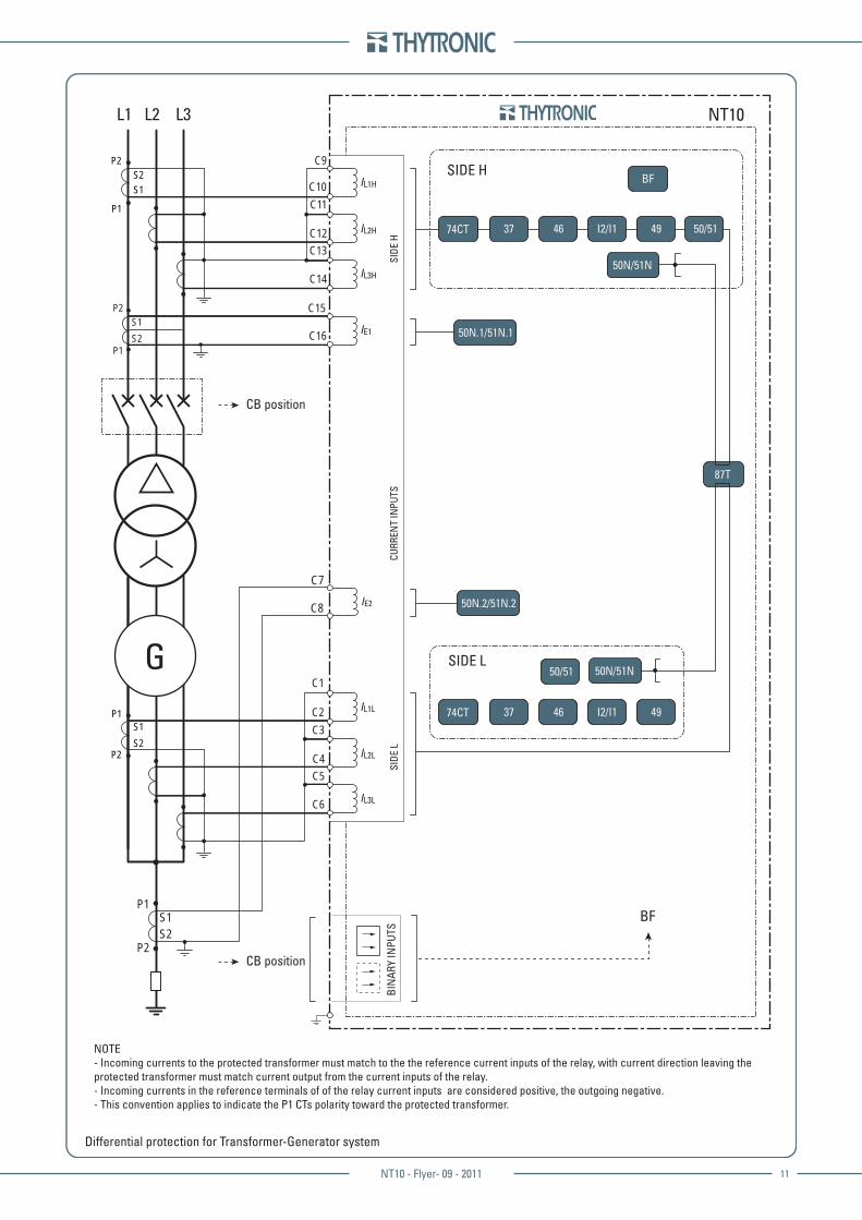
Differential protection for Transformer-Generator system
C10
C9
C11
C12C13
C14
P1S1S2
P2
IL1L
IL2L
IL3L
C2
C1
C3
C4C5
C6
P1
S1S2
P2
IL1H
IL2H
IL3H
P1S1S2
P2
IE2
C7
C8
50N/51N
C15
C16 IE1
P1
S1S2
P2
50N.1/51N.1
BF
74CT 4637 49 50/51I2/I1
50N/51N
50N.2/51N.2
74CT 4637 49
50/51
I2/I1
G
NOTE- Incoming currents to the protected transformer must match to the the reference current inputs of the relay, with current direction leaving the protected transformer must match current output from the current inputs of the relay.- Incoming currents in the reference terminals of of the relay current inputs are considered positive, the outgoing negative.- This convention applies to indicate the P1 CTs polarity toward the protected transformer.
Headquarter: 20139 Milano - Piazza Mistral, 7 - Tel. +39 02 574 957 01 ra - Fax +39 02 574 037 63Factory: 35127 Padova - Z.I. Sud - Via dell’Artigianato, 48 - Tel. +39 049 894 770 1 ra - Fax +39 049 870 139 0
www.thytronic.it www.thytronic.com [email protected]
D I M E N S I O N S
101
171
149
128.5110
200
168
20
ø 4.5
F1
D1
RX
TX
F2F3F4F5
A1A2
A3A4A5
A6A7A8
A9A10A11
A12A13A14
A15A16
A17A18
A19A20
A21A22
B1B2B3B4B5B6B7B8
E1
19
C
210
311
412
513
614
715
816
F1
D1
RX
TX
F2F3F4F5
A1A2
A3A4A5
A6A7A8
A9A10A11
A12A13A14
A15A16
A17A18
A19A20
A21A22
B1B2B3B4B5B6B7B8
E1
19
C
210
311
412
513
614
715
816
120
8031
205 30530
107
177
ø 4.5
102.5 ±0.370
161
154
ø 4.5
212.525 15
170
275
177
(4U)
101.
6
482.6465
ON 41 32 5
TRIP
START
ON 41 32 5
TRIP
START ON 41 32 5
TRIP
START
ON 41 32 5
TRIP
START ON 41 32 5
TRIP
START ON 41 32 5
TRIP
START
FLUSH MOUNTING PROJECTING MOUNTING FLUSH MOUNTING PROJECTING MOUNTING(Separate operator panel)
FLUSH MOUNTING SEPARATEOPERATOR PANEL
PROJECTING MOUNTINGPROJECTING MOUNTING(Stand alone)(Separate operator panel)
N.4 holes ø 3.5
RACK MOUNTING FLUSH MOUNTING CUTOUT
SIDE VIEW
FRONT VIEW REAR VIEW