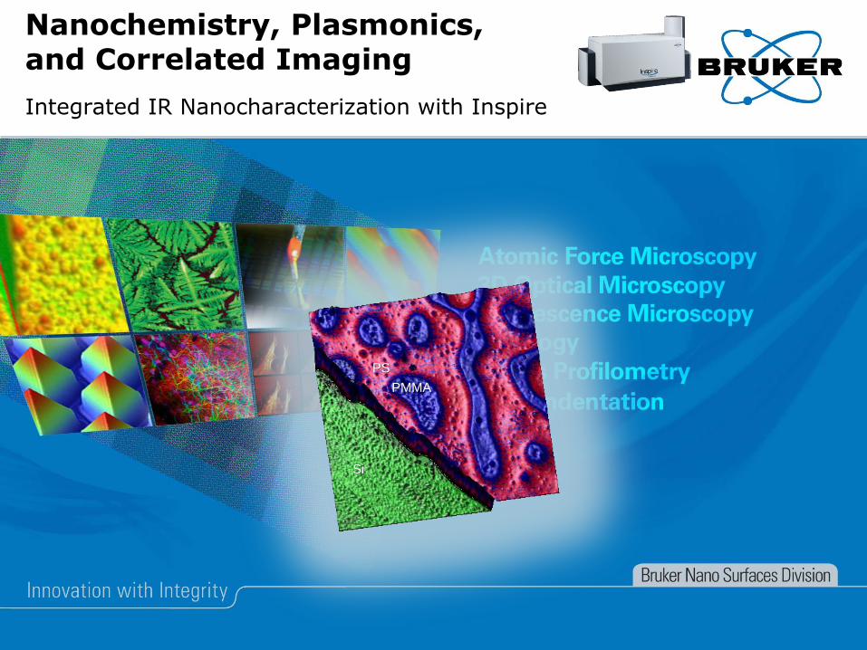
Nanochemistry, Plasmonics, and Correlated Imaging
Integrated IR Nanocharacterization with Inspire
Si
PS
PMMA

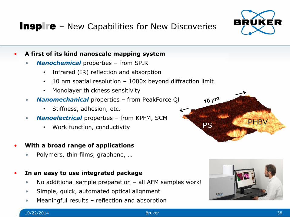
Inspire – New Capabilities for New Discoveries
2 10/22/2014 Bruker
PS PHBV
• A first of its kind nanoscale mapping system
• Nanochemical properties – from SPIR
• Infrared (IR) reflection and absorption
• 10 nm spatial resolution – 1000x beyond diffraction limit
• Monolayer thickness sensitivity
• Nanomechanical properties – from PeakForce QNM
• Stiffness, adhesion, etc.
• Nanoelectrical properties – from KPFM, SCM
• Work function, conductivity
• With a broad range of applications
• Polymers, thin films, graphene, …
• In an easy to use integrated package
• No additional sample preparation – all AFM samples work!
• Simple, quick, automated optical alignment
• Meaningful results – reflection and absorption
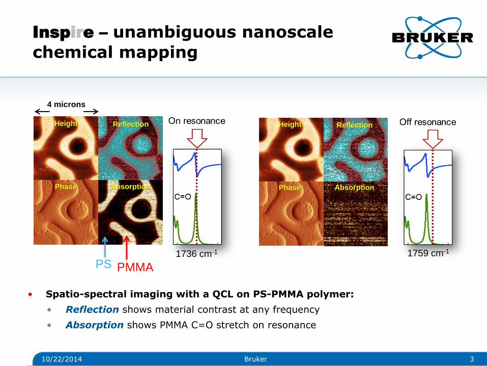
Inspire – unambiguous nanoscale
chemical mapping
3
Spatio-spectral imaging on PS-PMMA polymer:
PS-PMMA blend. Reflection shows material contrast at any frequency. Absorption identifies PMMA on resonance. Here using the 100cm-1 range of a QCL centered at 1730cm-1 to move
on and off the 1736cm-1 carbonyl resonance of PMMA. Image size 4 microns.
Height
Phase
Reflection
Absorption
1759 cm-1
10/22/2014 Bruker
Height
Phase
Reflection
Absorption
1736 cm-1
PS PMMA
4 microns
• Spatio-spectral imaging with a QCL on PS-PMMA polymer:
• Reflection shows material contrast at any frequency
• Absorption shows PMMA C=O stretch on resonance
4 10/22/2014 Bruker
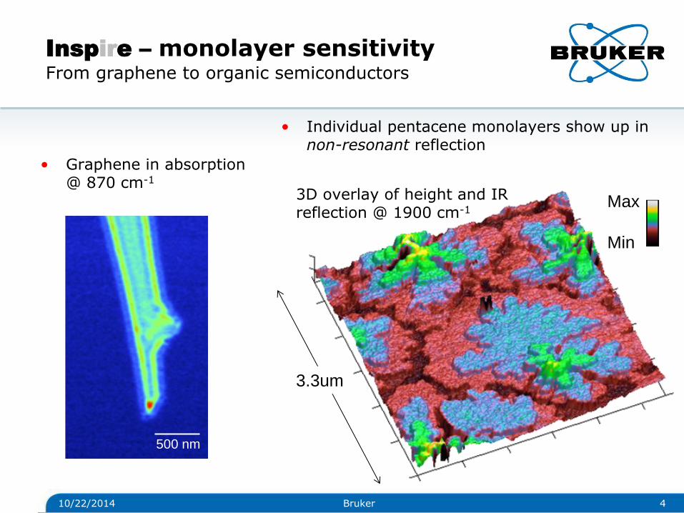
Inspire – monolayer sensitivity From graphene to organic semiconductors
500 nm
• Graphene in absorption @ 870 cm-1
3.3um
Max
Min
• Individual pentacene monolayers show up in non-resonant reflection
3D overlay of height and IR reflection @ 1900 cm-1
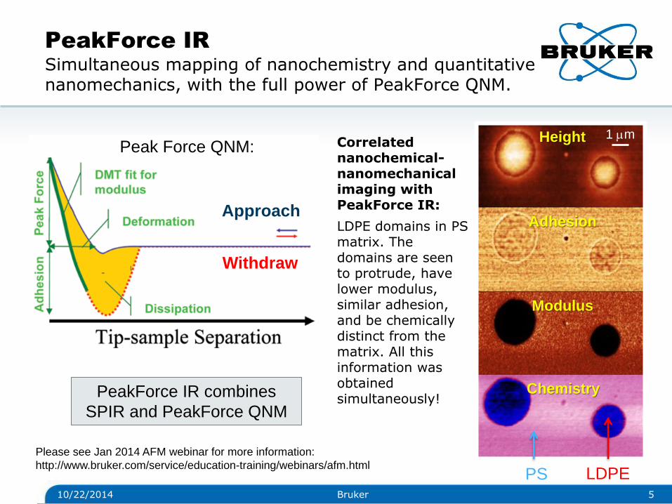
PeakForce IR
Simultaneous mapping of nanochemistry and quantitative nanomechanics, with the full power of PeakForce QNM.
5
Correlated nanochemical-nanomechanical imaging with PeakForce IR:
LDPE domains in PS matrix. The domains are seen to protrude, have lower modulus, similar adhesion, and be chemically distinct from the matrix. All this information was obtained simultaneously! PeakForce IR combines
SPIR and PeakForce QNM
10/22/2014 Bruker
Approach
Withdraw
Height
Adhesion
Modulus
Chemistry
PS LDPE
1 mm Peak Force QNM:
Please see Jan 2014 AFM webinar for more information:
http://www.bruker.com/service/education-training/webinars/afm.html
Exclusive Measurement Breadth
Combine IR nanochemical mapping with Bruker exclusive electrical measurements including mV level workfunction measurements and conductivity on soft samples.
6
Inspire provides the widest set of
new & exclusive capabilities.
What will you discover?
PeakForce IR:
SPIR imaging, here
shown for graphene at
1730cm-1, showing the
expected layer ordering
in universal
conductivity regime’
PeakForce KPFM
work function imaging with
mV sensitivity, here shown
for reduced graphene
oxide. Revealing <20nm
potential variations due to
chemical heterogeneity.
PeakForce QNM
nanomechanical
imaging with
atomic defect
resolution, shown
here on calcite.
PeakForce TUNA
conductivity imaging,
shown here on
vertically standing
carbon nanotubes.
Impossible with
contact mode.
Height Conductivity
10/22/2014 Bruker
10 nm
750 nm 1 mm
15 mm

Introducing Inspire
7
Introduction to the Technique
PS-PMMA: Absorption at 1730cm-1, 5 micron image.
10/22/2014 Bruker
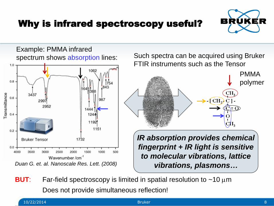
Why is infrared spectroscopy useful?
10/22/2014 8 Bruker
IR absorption provides chemical
fingerprint + IR light is sensitive
to molecular vibrations, lattice
vibrations, plasmons…
Example: PMMA infrared
spectrum shows absorption lines:
Duan G. et. al. Nanoscale Res. Lett. (2008)
PMMA
polymer
Bruker Tensor
Such spectra can be acquired using Bruker
FTIR instruments such as the Tensor
BUT: Far-field spectroscopy is limited in spatial resolution to ~10 mm
Does not provide simultaneous reflection!
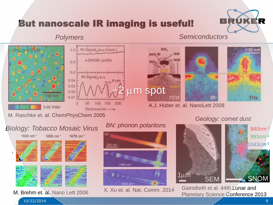
But nanoscale IR imaging is useful!
10/22/2014
Bruker
9
7.5um
7.5um x 7.5um
A.J. Huber et. al. NanoLett 2008
Biology: Tobacco Mosaic Virus
M. Brehm et. al. Nano Lett 2006
Semiconductors
Geology: comet dust
Gainsforth et al. 44th Lunar and
Planetary Science Conference 2013
1mm SEM SNOM
1043cm-1
940cm-1
993cm-1
Polymers
50nm x 50nm
PS-b-P2VP
M. Raschke et. al. ChemPhysChem 2005
BN: phonon polaritons
X. Xu et. al. Nat. Comm. 2014
~2 mm spot
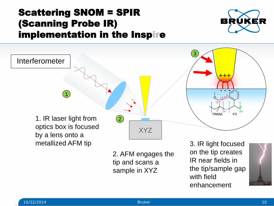
Scattering SNOM = SPIR
(Scanning Probe IR)
implementation in the Inspire
10/22/2014 10 Bruker
XYZ
1. IR laser light from
optics box is focused
by a lens onto a
metallized AFM tip
1
2
3
2. AFM engages the
tip and scans a
sample in XYZ
3. IR light focused
on the tip creates
IR near fields in
the tip/sample gap
with field
enhancement
+++
- - -
Interferometer
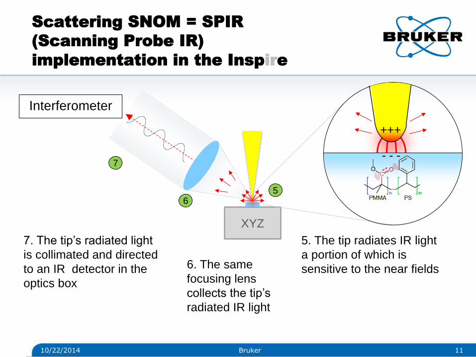
10/22/2014 11 Bruker
XYZ
+++
- - - 7
6 5
5. The tip radiates IR light
a portion of which is
sensitive to the near fields 6. The same
focusing lens
collects the tip’s
radiated IR light
7. The tip’s radiated light
is collimated and directed
to an IR detector in the
optics box
Interferometer
Scattering SNOM = SPIR
(Scanning Probe IR)
implementation in the Inspire

10/22/2014 12 Bruker
XYZ
+++
- - - 7
6 5
Interferometer
Scattering SNOM = SPIR
(Scanning Probe IR)
implementation in the Inspire
Localization to ~ 10 nm
(tip radius), independent
of l!
Imaging with
PeakForce QNM,
KPFM, …!
Infrared absorption
and reflection!
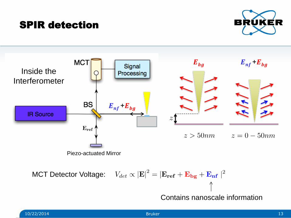
MCT Detector Voltage:
Contains nanoscale information
𝑬𝒏𝒇 +𝑬𝒃𝒈 𝑬𝒃𝒈
10/22/2014 Bruker 13
𝑬𝒏𝒇 +𝑬𝒃𝒈
Inside the
Interferometer
Piezo-actuated Mirror
SPIR detection
14
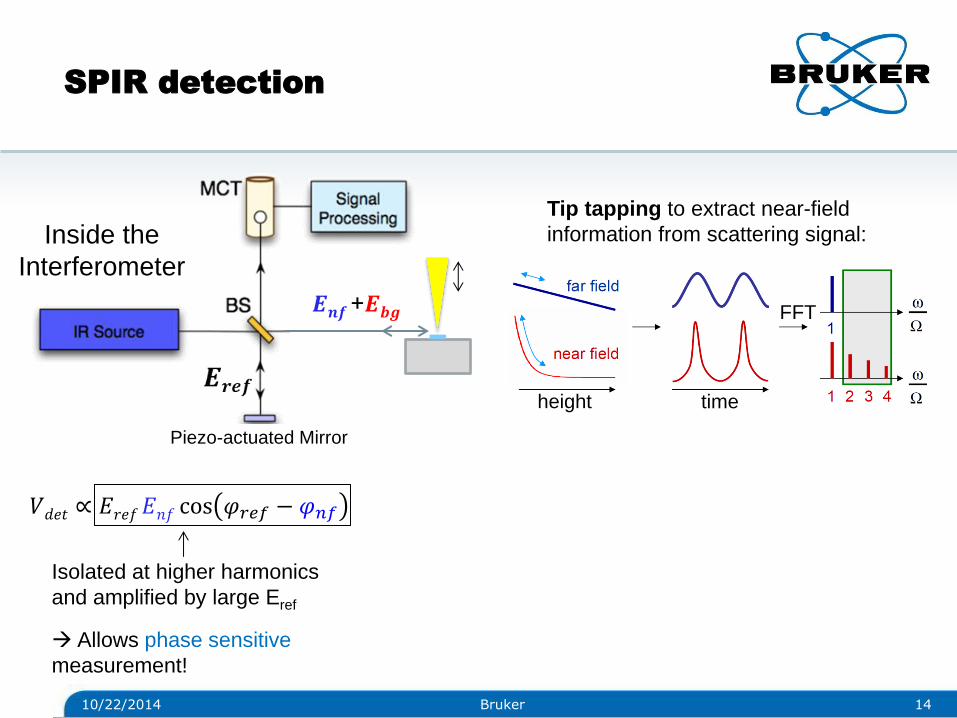
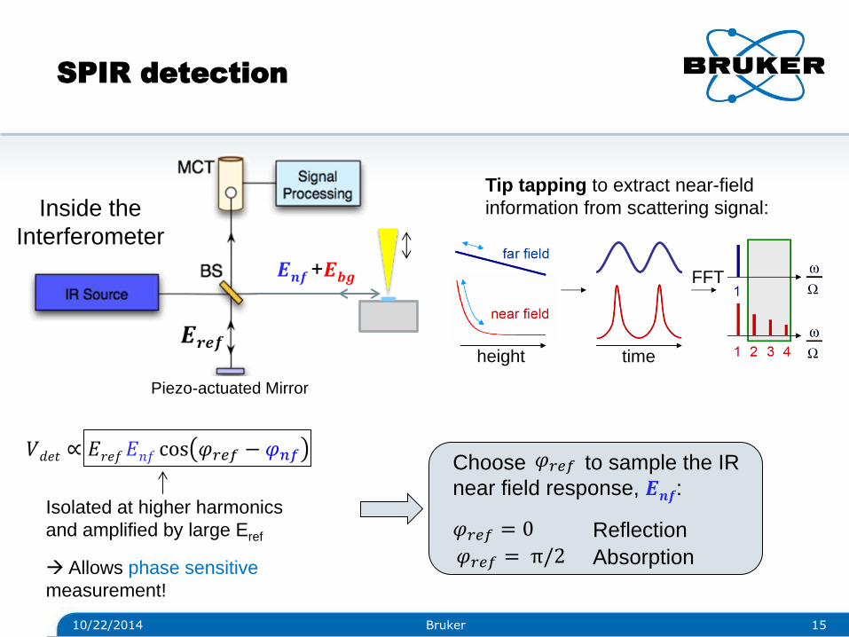
𝑉𝑑𝑒𝑡 ∝ 𝐸𝑟𝑒𝑓 𝐸𝑛𝑓 cos 𝜑𝑟𝑒𝑓 − 𝜑𝑛𝑓 + 𝐸𝑏𝑔𝐸𝑛𝑓 cos 𝜑𝑏𝑔 − 𝜑𝑛𝑓 + 𝐸𝑟𝑒𝑓𝐸𝑏𝑔 cos 𝜑𝑟𝑒𝑓 − 𝜑𝑏𝑔
+ 𝐸𝑟𝑒𝑓2 + |𝐸𝑛𝑓|2 + |𝐸𝑏𝑔|2
Isolated at higher harmonics
and amplified by large Eref
Allows phase sensitive
measurement!
Negligible
compared to Eref Suppressed at
higher harmonics
10/22/2014 Bruker
SPIR detection
Tip tapping to extract near-field
information from scattering signal:
height time
FFT 𝑬𝒏𝒇 +𝑬𝒃𝒈
Inside the
Interferometer
Piezo-actuated Mirror
15
𝑉𝑑𝑒𝑡 ∝ 𝐸𝑟𝑒𝑓 𝐸𝑛𝑓 cos 𝜑𝑟𝑒𝑓 − 𝜑𝑛𝑓
Isolated at higher harmonics
and amplified by large Eref
Allows phase sensitive
measurement!
10/22/2014 Bruker
SPIR detection
Choose to sample the IR
near field response, 𝑬𝒏𝒇:
Reflection
Absorption
𝜑𝑟𝑒𝑓 = 0
𝜑𝑟𝑒𝑓 = π/2
𝜑𝑟𝑒𝑓
height time
FFT 𝑬𝒏𝒇 +𝑬𝒃𝒈
Inside the
Interferometer
Piezo-actuated Mirror
Tip tapping to extract near-field
information from scattering signal:
SPIR with Inspire
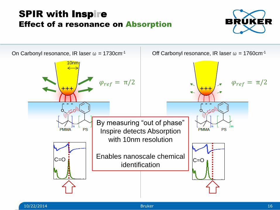
Effect of a resonance on Absorption
+++
- - -
On Carbonyl resonance, IR laser ω = 1730cm-1
C=O
Off Carbonyl resonance, IR laser ω = 1760cm-1
+++
- - -
C=O
By measuring “out of phase”
Inspire detects Absorption
with 10nm resolution
Enables nanoscale chemical
identification
16
𝜑𝑟𝑒𝑓 = π/2 𝜑𝑟𝑒𝑓 = π/2
10nm
10/22/2014 Bruker

SPIR with Inspire
Effect of a resonance on Reflection
+++
- - -
On Carbonyl resonance, IR laser ω = 1720cm-1
C=O
Off Carbonyl resonance, IR laser ω = 1760cm-1
+++
- - -
C=O
By measuring “in phase”
Inspire detects Reflection
with 10nm resolution
Information beyond ChemID:
Film Thickness
Conductivity
Plasmonics
17
𝜑𝑟𝑒𝑓 = 0 𝜑𝑟𝑒𝑓 = 0
10nm
10/22/2014 Bruker
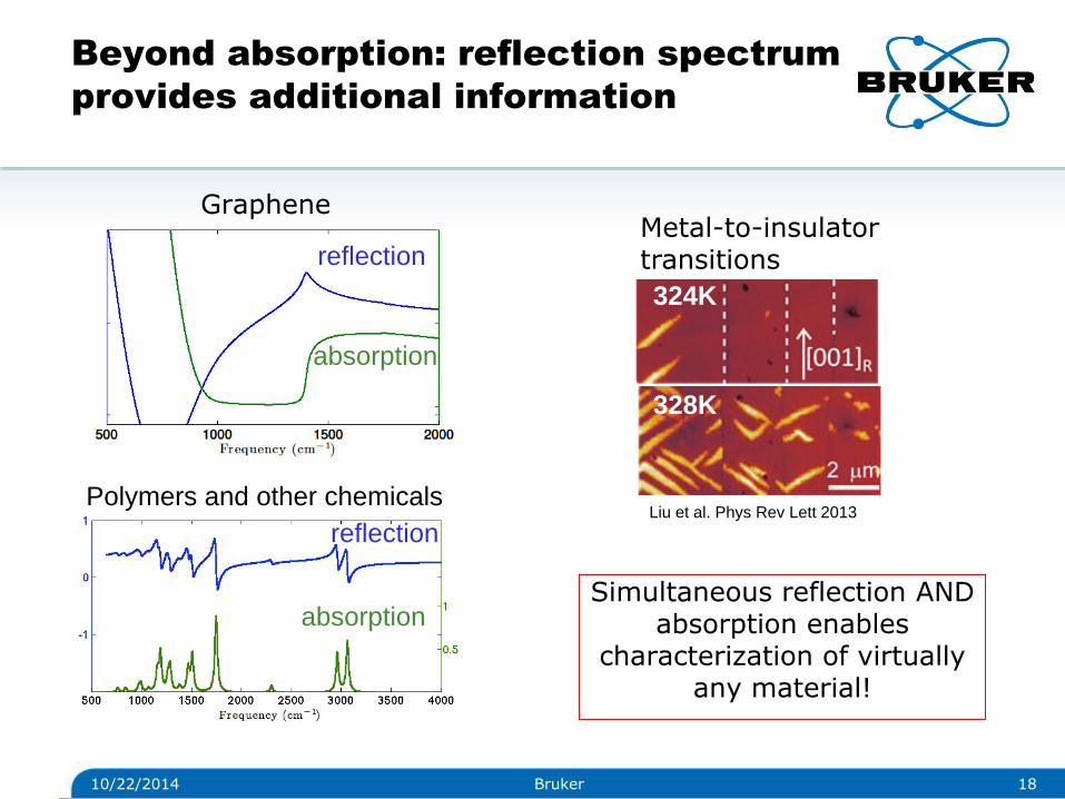
Beyond absorption: reflection spectrum
provides additional information
18
Graphene
Simultaneous reflection AND absorption enables
characterization of virtually any material!
Polymers and other chemicals
10/22/2014 Bruker
reflection
reflection
absorption
absorption
Bruker
50nm x 50nm
324K
328K
Metal-to-insulator transitions
Liu et al. Phys Rev Lett 2013
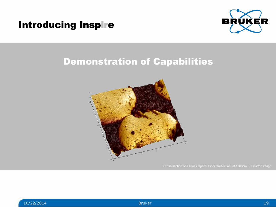
Introducing Inspire
19
Demonstration of Capabilities
Cross-section of a Glass Optical Fiber :Reflection at 1900cm-1, 5 micron image.
10/22/2014 Bruker

10nm-resolved IR reflection map
20
10nm spatial resolution:
Resolving 10nm features in IR reflection at 1933cm-1 on Si/SiO2 grating.
10 microns 1 micron 250 nm
10nm
10/22/2014 Bruker
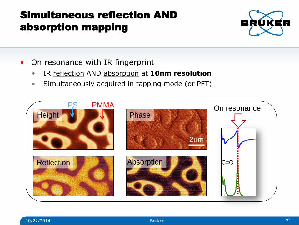
Simultaneous reflection AND
absorption mapping
• On resonance with IR fingerprint
• IR reflection AND absorption at 10nm resolution
• Simultaneously acquired in tapping mode (or PFT)
21
Reflection Absorption
Height Phase On resonance PMMA PS
2um
C=O
10/22/2014 Bruker
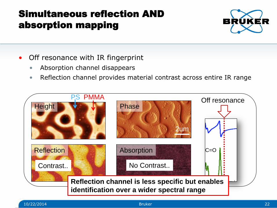
Simultaneous reflection AND
absorption mapping
• Off resonance with IR fingerprint
• Absorption channel disappears
• Reflection channel provides material contrast across entire IR range
22
Reflection Absorption
Height Phase Off resonance PMMA PS
No Contrast.. Contrast..
Reflection channel is less specific but enables
identification over a wider spectral range
2um
C=O
10/22/2014 Bruker
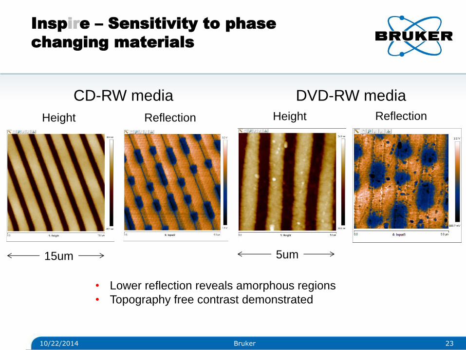
Inspire – Sensitivity to phase
changing materials
10/22/2014 23 Bruker
CD-RW media
Height Reflection
15um
Height
5um
Reflection
DVD-RW media
• Lower reflection reveals amorphous regions
• Topography free contrast demonstrated
PeakForce IR: simultaneous
nanomechanical and optical imaging
24
Height Adhesion
Modulus Deformation
QNM images of PS/LDPE blend
PeakForce IR - the only method for simultaneous, quantitative,
nanomechanical AND nanooptical characterization
Simultaneous IR
10/22/2014 Bruker
PS
Re(rp) ~ 0.12
LDPE
Re(rp) ~ 0.07
IR Reflection
0.04
0.16
Re(rp)
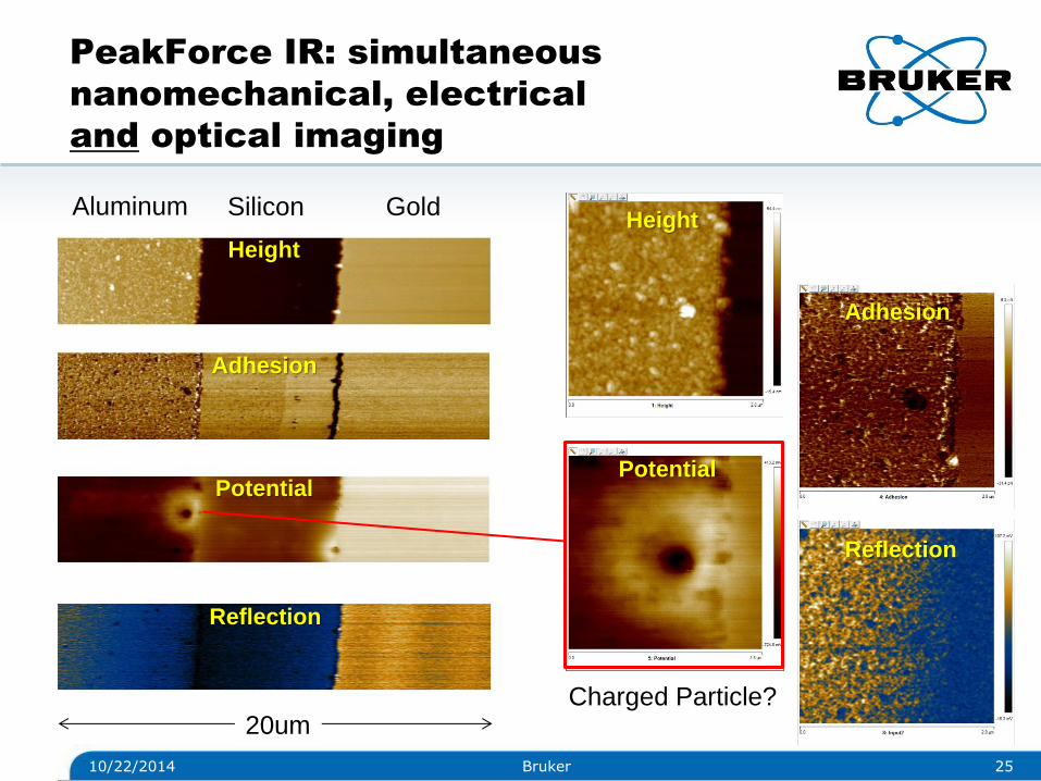
PeakForce IR: simultaneous
nanomechanical, electrical
and optical imaging
25 10/22/2014 Bruker
Height
Adhesion
Potential
Reflection
Aluminum Silicon Gold
20um
Height
Potential
Adhesion
Charged Particle?
Reflection
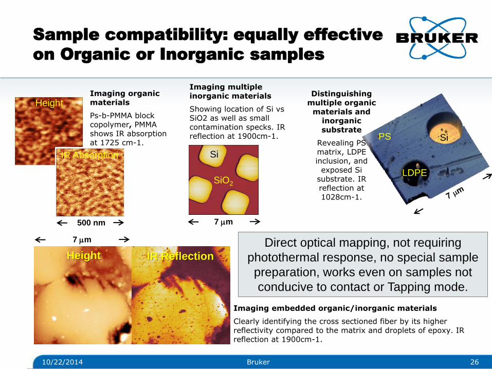
Sample compatibility: equally effective
on Organic or Inorganic samples
26
PS
LDPE
Si
Height IR Reflection
Imaging embedded organic/inorganic materials
Clearly identifying the cross sectioned fiber by its higher reflectivity compared to the matrix and droplets of epoxy. IR reflection at 1900cm-1.
Distinguishing multiple organic
materials and inorganic substrate
Revealing PS matrix, LDPE inclusion, and
exposed Si substrate. IR reflection at 1028cm-1.
Imaging multiple inorganic materials
Showing location of Si vs SiO2 as well as small contamination specks. IR reflection at 1900cm-1.
Si
SiO2
Direct optical mapping, not requiring
photothermal response, no special sample
preparation, works even on samples not
conducive to contact or Tapping mode.
10/22/2014 Bruker
Height
IR Absorption
500 nm
Imaging organic materials
Ps-b-PMMA block copolymer, PMMA shows IR absorption at 1725 cm-1.
7 mm
7 mm
SPIR characterization
of Graphene
27
Reflection
Absorption
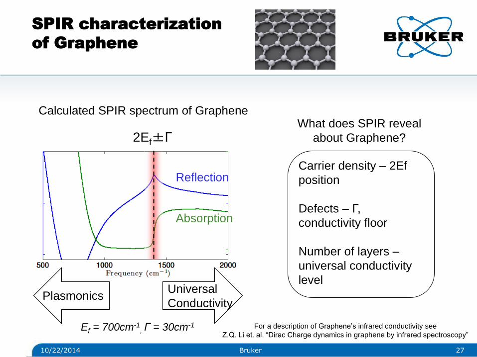
2Ef±Γ
Universal
Conductivity Plasmonics
Ef = 700cm-1, Γ = 30cm-1
Carrier density – 2Ef
position
Defects – Γ,
conductivity floor
Number of layers –
universal conductivity
level
Calculated SPIR spectrum of Graphene What does SPIR reveal
about Graphene?
10/22/2014 Bruker
For a description of Graphene’s infrared conductivity see
Z.Q. Li et. al. “Dirac Charge dynamics in graphene by infrared spectroscopy”
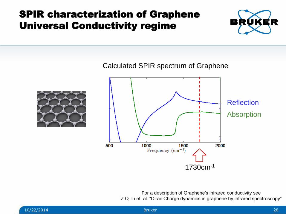
SPIR characterization of Graphene
Universal Conductivity regime
10/22/2014 28 Bruker
Reflection
Absorption
Calculated SPIR spectrum of Graphene
For a description of Graphene’s infrared conductivity see
Z.Q. Li et. al. “Dirac Charge dynamics in graphene by infrared spectroscopy”
1730cm-1
10/22/2014 29 Bruker
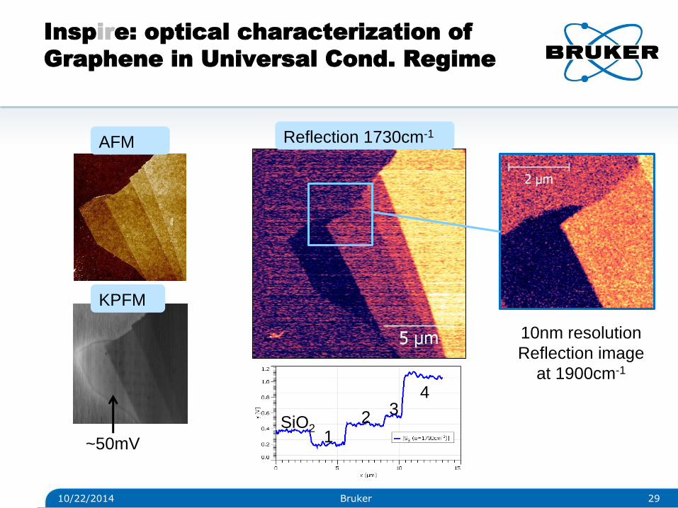
Reflection 1730cm-1
10nm resolution
Reflection image
at 1900cm-1
SiO2 1
2 3
4
AFM
KPFM
~50mV
Inspire: optical characterization of
Graphene in Universal Cond. Regime

10/22/2014 30 Bruker
Inspire: optical characterization of
Graphene - defect detection
Nanomechanics shows signs of wrinkles
Hint of
defects in
D-band
Raman
SPIR
reflection
signal
consistent with
higher defect
concentration
2% lower
IR Reflection
1900cm-1
2% lower
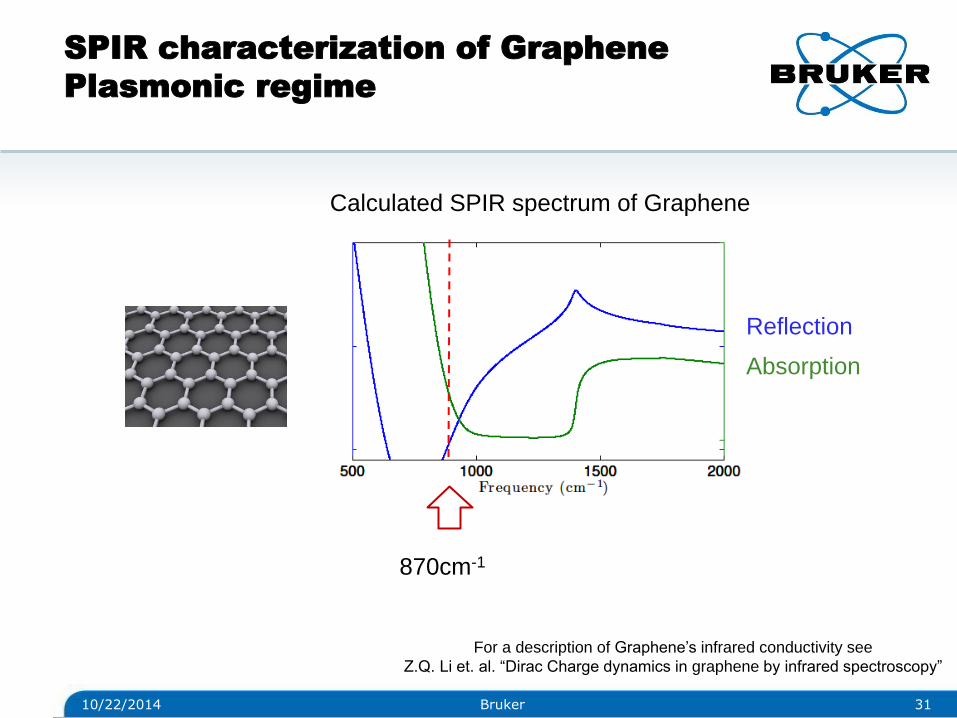
SPIR characterization of Graphene
Plasmonic regime
10/22/2014 31 Bruker
Reflection
Absorption
Calculated SPIR spectrum of Graphene
For a description of Graphene’s infrared conductivity see
Z.Q. Li et. al. “Dirac Charge dynamics in graphene by infrared spectroscopy”
870cm-1
SPIR characterization of Graphene Plasmonic regime
10/22/2014 32 Bruker
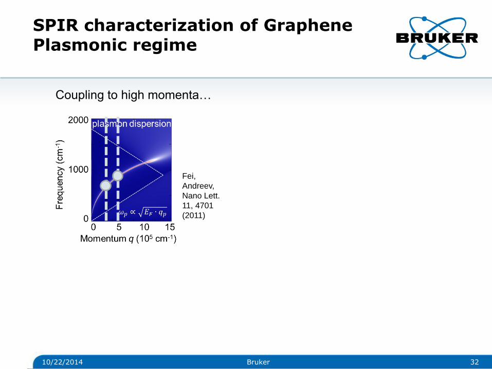
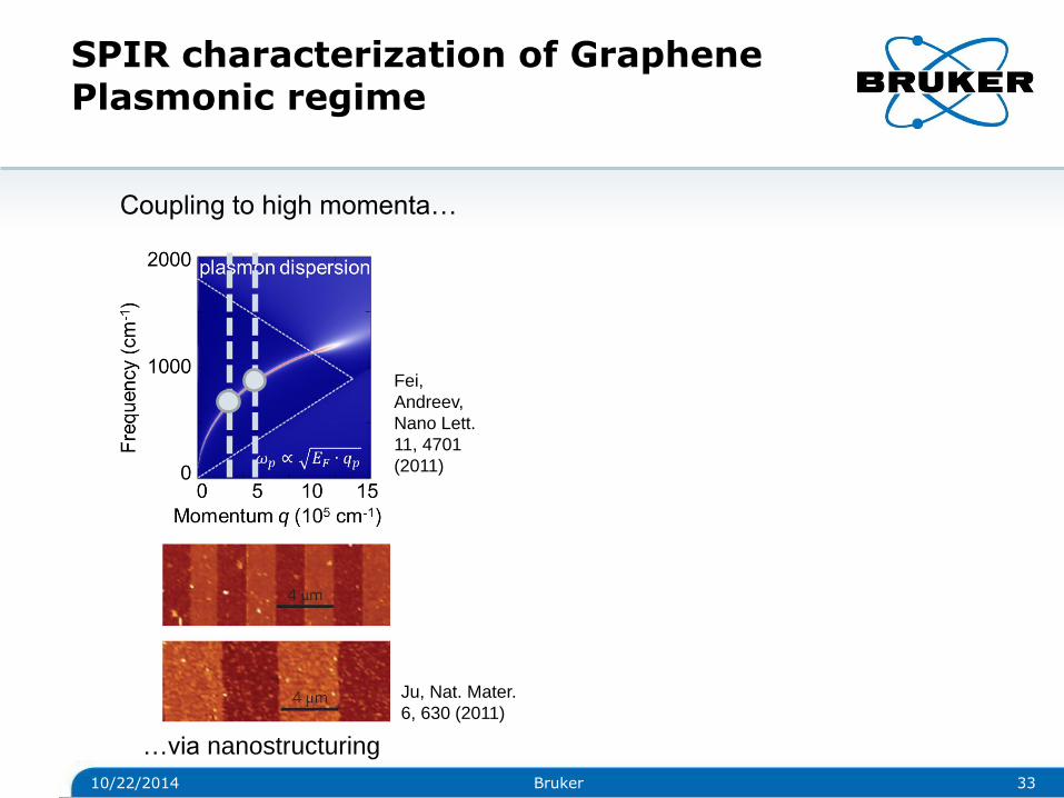
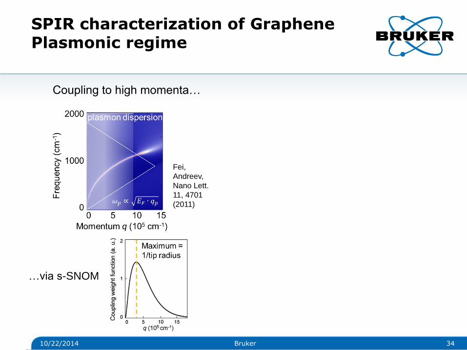
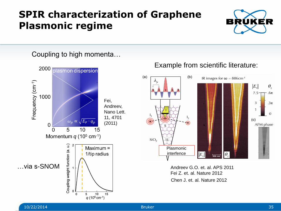
Fei,
Andreev,
Nano Lett.
11, 4701
(2011)
Coupling to high momenta…
SPIR characterization of Graphene Plasmonic regime
10/22/2014 33 Bruker
…via nanostructuring
Ju, Nat. Mater.
6, 630 (2011)
Fei,
Andreev,
Nano Lett.
11, 4701
(2011)
Coupling to high momenta…
SPIR characterization of Graphene Plasmonic regime
10/22/2014 34 Bruker
Fei,
Andreev,
Nano Lett.
11, 4701
(2011)
Coupling to high momenta…
…via s-SNOM
SPIR characterization of Graphene Plasmonic regime
10/22/2014 35 Bruker
Fei,
Andreev,
Nano Lett.
11, 4701
(2011)
Coupling to high momenta…
…via s-SNOM
Plasmonic
interfence
Andreev G.O. et. al. APS 2011
Fei Z. et. al. Nature 2012
Chen J. et. al. Nature 2012
Example from scientific literature:
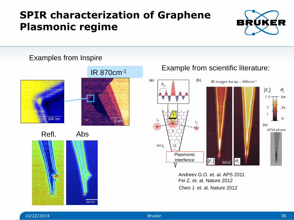
SPIR characterization of Graphene Plasmonic regime
10/22/2014 36 Bruker
500 nm
Refl. Abs
Examples from Inspire
IR 870cm-1
Plasmonic
interfence
Andreev G.O. et. al. APS 2011
Fei Z. et. al. Nature 2012
Chen J. et. al. Nature 2012
Example from scientific literature:
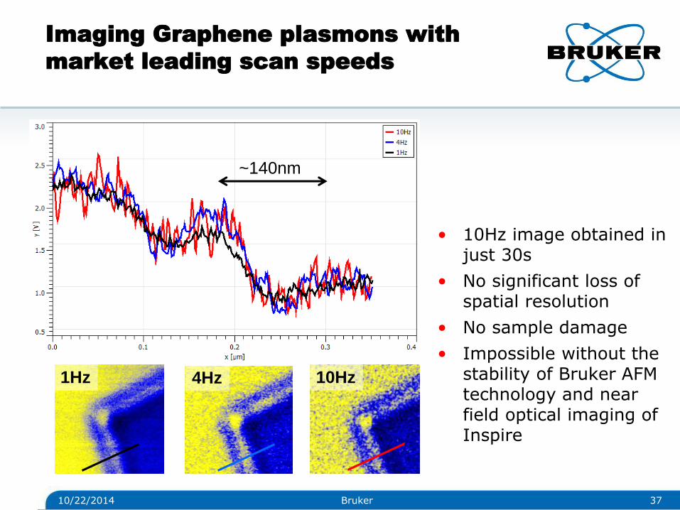
Imaging Graphene plasmons with
market leading scan speeds
• 10Hz image obtained in just 30s
• No significant loss of spatial resolution
• No sample damage
• Impossible without the stability of Bruker AFM technology and near field optical imaging of Inspire
1Hz 4Hz 10Hz
~140nm
10/22/2014 Bruker 37
• A first of its kind nanoscale mapping system
• Nanochemical properties – from SPIR
• Infrared (IR) reflection and absorption
• 10 nm spatial resolution – 1000x beyond diffraction limit
• Monolayer thickness sensitivity
• Nanomechanical properties – from PeakForce QNM
• Stiffness, adhesion, etc.
• Nanoelectrical properties – from KPFM, SCM
• Work function, conductivity
• With a broad range of applications
• Polymers, thin films, graphene, …
• In an easy to use integrated package
• No additional sample preparation – all AFM samples work!
• Simple, quick, automated optical alignment
• Meaningful results – reflection and absorption
Inspire – New Capabilities for New Discoveries
38 10/22/2014 Bruker
PS PHBV

© Copyright Bruker Corporation. All rights reserved.
www.bruker.com


![Nanochemistry Chapter 1 Ozin Arsenault 2005[1]](https://static.cupdf.com/doc/110x72/563db8c8550346aa9a96e61e/nanochemistry-chapter-1-ozin-arsenault-20051.jpg)


![INVITED PAPER QuantumPlasmonics€¦ · ters near plasmonic structures [20], graphene plasmonics [21], semiconductor plasmonics [22], hot electrons [23], and active quantum plasmonics](https://static.cupdf.com/doc/110x72/5f0859367e708231d4219104/invited-paper-quantumplasmonics-ters-near-plasmonic-structures-20-graphene-plasmonics.jpg)