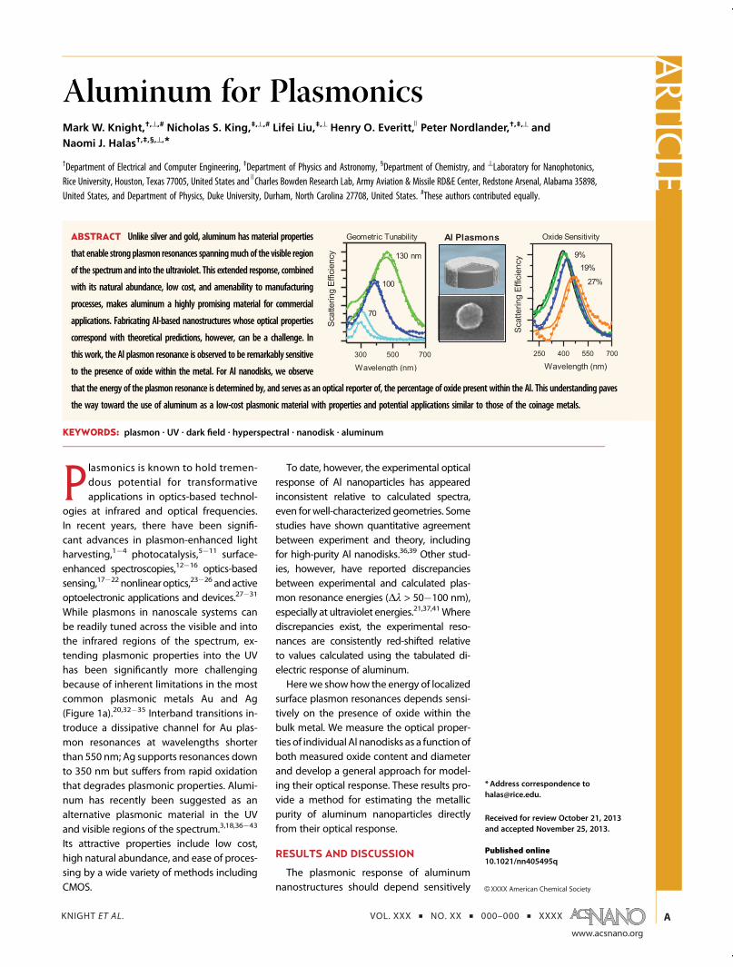
KNIGHT ET AL. VOL. XXX ’ NO. XX ’ 000–000 ’ XXXX www.acsnano.org A C XXXX American Chemical Society Aluminum for Plasmonics Mark W. Knight, †,^,# Nicholas S. King, ‡,^,# Lifei Liu, ‡,^ Henry O. Everitt, ) Peter Nordlander, †,‡,^ and Naomi J. Halas †,‡,§,^, * † Department of Electrical and Computer Engineering, ‡ Department of Physics and Astronomy, § Department of Chemistry, and ^ Laboratory for Nanophotonics, Rice University, Houston, Texas 77005, United States and ) Charles Bowden Research Lab, Army Aviation & Missile RD&E Center, Redstone Arsenal, Alabama 35898, United States, and Department of Physics, Duke University, Durham, North Carolina 27708, United States. # These authors contributed equally. P lasmonics is known to hold tremen- dous potential for transformative applications in optics-based technol- ogies at infrared and optical frequencies. In recent years, there have been signifi- cant advances in plasmon-enhanced light harvesting, 14 photocatalysis, 511 surface- enhanced spectroscopies, 1216 optics-based sensing, 1722 nonlinear optics, 2326 and active optoelectronic applications and devices. 2731 While plasmons in nanoscale systems can be readily tuned across the visible and into the infrared regions of the spectrum, ex- tending plasmonic properties into the UV has been significantly more challenging because of inherent limitations in the most common plasmonic metals Au and Ag (Figure 1a). 20,3235 Interband transitions in- troduce a dissipative channel for Au plas- mon resonances at wavelengths shorter than 550 nm; Ag supports resonances down to 350 nm but suffers from rapid oxidation that degrades plasmonic properties. Alumi- num has recently been suggested as an alternative plasmonic material in the UV and visible regions of the spectrum. 3,18,3643 Its attractive properties include low cost, high natural abundance, and ease of proces- sing by a wide variety of methods including CMOS. To date, however, the experimental optical response of Al nanoparticles has appeared inconsistent relative to calculated spectra, even for well-characterized geometries. Some studies have shown quantitative agreement between experiment and theory, including for high-purity Al nanodisks. 36,39 Other stud- ies, however, have reported discrepancies between experimental and calculated plas- mon resonance energies (Δλ > 50100 nm), especially at ultraviolet energies. 21,37,41 Where discrepancies exist, the experimental reso- nances are consistently red-shifted relative to values calculated using the tabulated di- electric response of aluminum. Here we show how the energy of localized surface plasmon resonances depends sensi- tively on the presence of oxide within the bulk metal. We measure the optical proper- ties of individual Al nanodisks as a function of both measured oxide content and diameter and develop a general approach for model- ing their optical response. These results pro- vide a method for estimating the metallic purity of aluminum nanoparticles directly from their optical response. RESULTS AND DISCUSSION The plasmonic response of aluminum nanostructures should depend sensitively * Address correspondence to [email protected]. Received for review October 21, 2013 and accepted November 25, 2013. Published online 10.1021/nn405495q ABSTRACT Unlike silver and gold, aluminum has material properties that enable strong plasmon resonances spanning much of the visible region of the spectrum and into the ultraviolet. This extended response, combined with its natural abundance, low cost, and amenability to manufacturing processes, makes aluminum a highly promising material for commercial applications. Fabricating Al-based nanostructures whose optical properties correspond with theoretical predictions, however, can be a challenge. In this work, the Al plasmon resonance is observed to be remarkably sensitive to the presence of oxide within the metal. For Al nanodisks, we observe that the energy of the plasmon resonance is determined by, and serves as an optical reporter of, the percentage of oxide present within the Al. This understanding paves the way toward the use of aluminum as a low-cost plasmonic material with properties and potential applications similar to those of the coinage metals. KEYWORDS: plasmon . UV . dark field . hyperspectral . nanodisk . aluminum ARTICLE

Welcome message from author
This document is posted to help you gain knowledge. Please leave a comment to let me know what you think about it! Share it to your friends and learn new things together.
Transcript
KNIGHT ET AL. VOL. XXX ’ NO. XX ’ 000–000 ’ XXXX
www.acsnano.org
A
CXXXX American Chemical Society
Aluminum for PlasmonicsMark W. Knight,†,^,# Nicholas S. King,‡,^,# Lifei Liu,‡,^ Henry O. Everitt, ) Peter Nordlander,†,‡,^ and
Naomi J. Halas†,‡,§,^,*
†Department of Electrical and Computer Engineering, ‡Department of Physics and Astronomy, §Department of Chemistry, and ^Laboratory for Nanophotonics,Rice University, Houston, Texas 77005, United States and )Charles Bowden Research Lab, Army Aviation & Missile RD&E Center, Redstone Arsenal, Alabama 35898,United States, and Department of Physics, Duke University, Durham, North Carolina 27708, United States. #These authors contributed equally.
Plasmonics is known to hold tremen-dous potential for transformativeapplications in optics-based technol-
ogies at infrared and optical frequencies.In recent years, there have been signifi-cant advances in plasmon-enhanced lightharvesting,1�4 photocatalysis,5�11 surface-enhanced spectroscopies,12�16 optics-basedsensing,17�22 nonlinear optics,23�26 andactiveoptoelectronic applications and devices.27�31
While plasmons in nanoscale systems canbe readily tuned across the visible and intothe infrared regions of the spectrum, ex-tending plasmonic properties into the UVhas been significantly more challengingbecause of inherent limitations in the mostcommon plasmonic metals Au and Ag(Figure 1a).20,32�35 Interband transitions in-troduce a dissipative channel for Au plas-mon resonances at wavelengths shorterthan 550 nm; Ag supports resonances downto 350 nm but suffers from rapid oxidationthat degrades plasmonic properties. Alumi-num has recently been suggested as analternative plasmonic material in the UVand visible regions of the spectrum.3,18,36�43
Its attractive properties include low cost,high natural abundance, and ease of proces-sing by a wide variety of methods includingCMOS.
To date, however, the experimental opticalresponse of Al nanoparticles has appearedinconsistent relative to calculated spectra,even forwell-characterized geometries. Somestudies have shown quantitative agreementbetween experiment and theory, includingfor high-purity Al nanodisks.36,39 Other stud-ies, however, have reported discrepanciesbetween experimental and calculated plas-mon resonance energies (Δλ > 50�100 nm),especially at ultraviolet energies.21,37,41Wherediscrepancies exist, the experimental reso-nances are consistently red-shifted relativeto values calculated using the tabulated di-electric response of aluminum.Herewe showhow the energy of localized
surface plasmon resonances depends sensi-tively on the presence of oxide within thebulk metal. We measure the optical proper-ties of individual Al nanodisks as a function ofboth measured oxide content and diameterand develop a general approach for model-ing their optical response. These results pro-vide a method for estimating the metallicpurity of aluminum nanoparticles directlyfrom their optical response.
RESULTS AND DISCUSSION
The plasmonic response of aluminumnanostructures should depend sensitively
* Address correspondence [email protected].
Received for review October 21, 2013and accepted November 25, 2013.
Published online10.1021/nn405495q
ABSTRACT Unlike silver and gold, aluminum has material properties
that enable strong plasmon resonances spanningmuch of the visible region
of the spectrum and into the ultraviolet. This extended response, combined
with its natural abundance, low cost, and amenability to manufacturing
processes, makes aluminum a highly promising material for commercial
applications. Fabricating Al-based nanostructures whose optical properties
correspond with theoretical predictions, however, can be a challenge. In
this work, the Al plasmon resonance is observed to be remarkably sensitive
to the presence of oxide within the metal. For Al nanodisks, we observe
that the energy of the plasmon resonance is determined by, and serves as an optical reporter of, the percentage of oxide present within the Al. This understanding paves
the way toward the use of aluminum as a low-cost plasmonic material with properties and potential applications similar to those of the coinage metals.
KEYWORDS: plasmon . UV . dark field . hyperspectral . nanodisk . aluminum
ARTIC
LE
KNIGHT ET AL. VOL. XXX ’ NO. XX ’ 000–000 ’ XXXX
www.acsnano.org
B
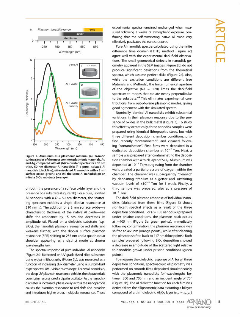
on both the presence of a surface oxide layer and thepresence of a substrate (Figure 1b). For a pure, isolatedAl nanodisk with a D = 50 nm diameter, the scatter-ing spectrum exhibits a single dipolar resonance at210 nm (i). The addition of a 3 nm surface oxide;acharacteristic thickness of the native Al oxide;redshifts the resonance by 15 nm and decreases itsamplitude (ii). Placed on a dielectric substrate (e.g.,SiO2), the nanodisk plasmon resonance red shifts andweakens further, with the dipolar surface plasmonresonance (SPR) shifting to 255 nm and a quadrupolarshoulder appearing as a distinct mode at shorterwavelengths (iii).The spectral response of pure individual Al nanodisks
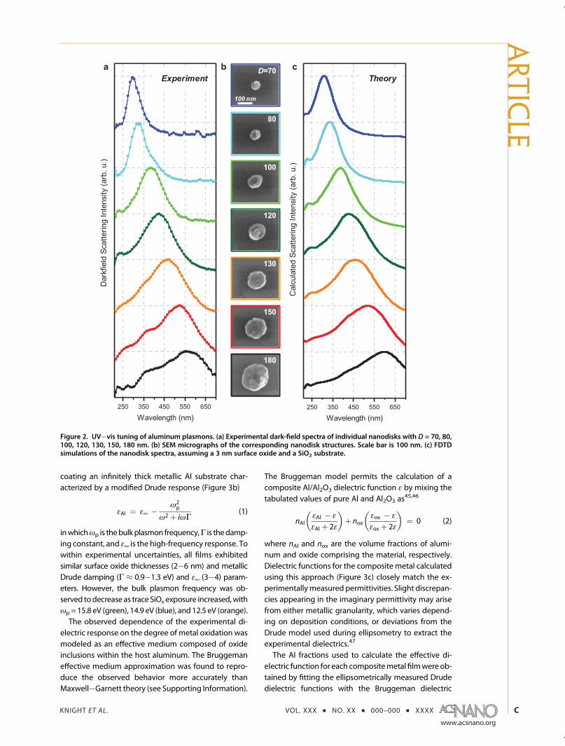
(Figure 2a), fabricated on UV-grade fused silica substratesusing e-beam lithography (Figure 2b), was measured as afunction of increasing disk diameter using a custom-builthyperspectral UV�visiblemicroscope. For small nanodisks,the deep UV plasmon resonance exhibits the characteristicLorentzian resonanceofadipolaroscillator.As thenanodiskdiameter is increased, phase delay across the nanoparticlecauses the plasmon resonance to red shift and broadenand introduces higher order, multipolar resonances. These
experimental spectra remained unchanged when mea-sured following 3 weeks of atmospheric exposure, con-firming that the self-terminating native Al oxide veryeffectively passivates the nanostructures.Pure Al nanodisk spectra calculated using the finite
difference time domain (FDTD) method (Figure 2c)agree well with the experimental dark-field observa-tions. The small geometrical defects in nanodisk ge-ometry apparent in the SEM images (Figure 2b) do notproduce significant deviations from the theoreticalspectra, which assume perfect disks (Figure 2c). Also,while the excitation conditions are different (seeMaterials and Methods), the finite numerical apertureof the objective (NA = 0.28) limits the dark-fieldspectrum to modes that radiate nearly perpendicularto the substrate.44 This eliminates experimental con-tributions from out-of-plane plasmonic modes, givinggood agreement with the simulated spectra.Nominally identical Al nanodisks exhibit substantial
variations in their plasmon response due to the pre-sence of oxides in the bulk metal (Figure 3). To studythis effect systematically, three nanodisk samples wereprepared using identical lithographic steps, but withthree different deposition chamber conditions: pris-tine, recently “contaminated”, and cleaned follow-ing “contamination”. First, films were deposited in adedicated deposition chamber at 10�7 Torr. Next, asample was prepared after contaminating the deposi-tion chamber with a thick layer of SiOx. Aluminumwasdeposited at 10�5 Torr; outgassing from the chamberwalls created a partial pressure of oxygen within thechamber. The chamber was subsequently “cleaned”by depositing titanium as a getter and sustainingvacuum levels of <10�5 Torr for 1 week. Finally, athird sample was prepared, also at a pressure of10�5 Torr.The dark-field plasmon response of individual nano-
disks fabricated from these films (Figure 3) showssignificant spectral effects as a result of the threedeposition conditions. For D = 100 nanodisks preparedunder pristine conditions, the plasmon peak occursat ∼405 nm (Figure 3a, green points). Immediatelyfollowing contamination, the plasmon resonance wasshifted to 465 nm (orange points), while after cleaningthe plasmon shifted back to 417 nm (blue points). Bothsamples prepared following SiOx deposition showeda decrease in amplitude of the scattered light relativeto nanodisks grown under pristine conditions (greenpoints).To measure the dielectric response of Al for all three
deposition conditions, spectroscopic ellipsometry wasperformed on smooth films deposited simultaneouslywith the plasmonic nanodisks for wavelengths be-tween 300 and 700 nm and an incident angle of 70�(Figure 3b). The Al dielectric function for each film wasderived from the ellipsometric data assuming a bilayercomposed of a thin dielectric Al2O3 layer (εox = εAl2O3
)
Figure 1. Aluminum as a plasmonic material. (a) Plasmontuning ranges of themost commonplasmonicmaterials, AuandAg, comparedwithAl. (b) Calculated spectra for a 35 nmthick, 50 nm diameter Al nanodisk: (i) a pure, isolated Alnanodisk (black line); (ii) an isolated Al nanodisk with a 3 nmsurface oxide (green); and (iii) the same Al nanodisk on aninfinite SiO2 substrate (orange).
ARTIC
LE
KNIGHT ET AL. VOL. XXX ’ NO. XX ’ 000–000 ’ XXXX
www.acsnano.org
C
coating an infinitely thick metallic Al substrate char-acterized by a modified Drude response (Figure 3b)
εAl ¼ ε¥ � ω2p
ω2 þ iωΓ(1)
inwhichωp is thebulkplasmon frequency,Γ is thedamp-ing constant, and ε¥ is the high-frequency response. Towithin experimental uncertainties, all films exhibitedsimilar surface oxide thicknesses (2�6 nm) and metallicDrude damping (Γ ≈ 0.9�1.3 eV) and ε¥ (3�4) param-eters. However, the bulk plasmon frequency was ob-served todecrease as trace SiOxexposure increased,withωp = 15.8 eV (green), 14.9 eV (blue), and12.5 eV (orange).The observed dependence of the experimental di-
electric response on the degree of metal oxidation wasmodeled as an effective medium composed of oxideinclusions within the host aluminum. The Bruggemaneffective medium approximation was found to repro-duce the observed behavior more accurately thanMaxwell�Garnett theory (see Supporting Information).
The Bruggeman model permits the calculation of acomposite Al/Al2O3 dielectric function ε by mixing thetabulated values of pure Al and Al2O3 as
45,46
nAlεAl � ε
εAl þ 2ε
� �þ nox
εox � ε
εox þ 2ε
� �¼ 0 (2)
where nAl and nox are the volume fractions of alumi-num and oxide comprising the material, respectively.Dielectric functions for the composite metal calculatedusing this approach (Figure 3c) closely match the ex-perimentallymeasured permittivities. Slight discrepan-cies appearing in the imaginary permittivity may arisefrom either metallic granularity, which varies depend-ing on deposition conditions, or deviations from theDrude model used during ellipsometry to extract theexperimental dielectrics.47
The Al fractions used to calculate the effective di-electric function for each compositemetalfilmwere ob-tained by fitting the ellipsometrically measured Drudedielectric functions with the Bruggeman dielectric
Figure 2. UV�vis tuning of aluminum plasmons. (a) Experimental dark-field spectra of individual nanodisks with D = 70, 80,100, 120, 130, 150, 180 nm. (b) SEM micrographs of the corresponding nanodisk structures. Scale bar is 100 nm. (c) FDTDsimulations of the nanodisk spectra, assuming a 3 nm surface oxide and a SiO2 substrate.
ARTIC
LE

KNIGHT ET AL. VOL. XXX ’ NO. XX ’ 000–000 ’ XXXX
www.acsnano.org
D
function, yielding nAl = 0.91 (green), 0.81 (blue), and0.73 (orange). Calculated nanodisk spectra using thesecomposite Al/Al2O3 dielectric functions for the coremetal and 3 nm of pure Al2O3 for the shell agree quiteclosely with the measured spectra (Figure 3a).The elemental composition of each film was con-
firmed under ultrahigh vacuum conditions using X-rayphotoelectron spectroscopy (XPS, PHI Quantera). Spec-tra were acquired for all elements present in the film/substrate system: Al 2p (68�80 eV), O 1s (526�538 eV),C 1s (280�292 eV), and Si 2p (97�109 eV). Using an AlKR X-ray source, the XPS measurements yielded aresponse limited to elements present within 10 nmof the exposed sample surface. The elemental compo-sition within the probe volume was obtained fromthe integrated XPS line shapes after accounting forinstrument- and material-dependent relative sensitiv-ity factors. The Al 2p spectrum contains two peakscorresponding to the oxidized and metallic states(75.7 and 73.5 eV).48,49 Given effective attenuationlengths of λAl = 2.92 nm and λox = 2.39 nm, whichare specific to Al 2p photoelectron emission,48 theratio of the integrated Al and Al2O3 peak intensitiesestimates the relative fractions of oxidized andmetallicaluminum within the penetration depth (∼3 λAl) of
the exposed surface. These relative intensities indicatesignificant differences in oxide content between thethree Al samples (Figure 4a).To determine the compositional depth profile of
the film, in situ Arþ etch cycles (3 kV, 3 � 3 mm area,12 s increments) and XPS measurements were per-formed iteratively to estimate the fractional composi-tion just below each freshly exposed surface. Significantaluminum and aluminum oxide peaks were observed(Figure 4a), allowing the depth profile of oxidized Al tobe measured quantitatively. In addition, the samplesexhibited aminor contribution from carbon;a surfacecontaminant only observed on the unetched films;and silicon, which only appeared when the etchingprocess had completely removed the 35 nm Alfilm from the Si substrate and the Al 2p peak haddisappeared. Otherwise, the only elements detectableduring depth profiling were aluminum and oxygen,with the oxygen appearing in a stoichiometric ratiowith aluminum consistent with the measured Al2O3.During the first several etch cycles, a rapid decreasein the Al2O3 peak was recorded, corresponding to theremoval of the passivating surface oxide (Figure 4d).Once the surface oxide layer was removed, the rest ofthefilmexhibitedaconstantbulkoxide fraction (Figure4b).
Figure 3. Aluminum dielectric response. (a) Scattering spectra of 100 nm diameter nanodisks with varying metal oxidefractions. The calculated spectra (solid lines) assume a 3 nm pure surface oxide and a SiO2 substrate. The experimental dark-field spectra (dotted lines, scaled for clarity) correspond to evaporations performed under exposure to varying trace levels ofoxygen, producing 9% (green), 19% (blue), and 27% (orange) metal oxide content. (b) Ellipsometrically measured dielectricfunctions for the three deposited Al purities. (c) Bruggeman dielectric functions for Al oxide fractions of 0% (black), 9%(green), 19% (blue), 27% (orange), 40% (gray), and 50% (light gray).
ARTIC
LE

KNIGHT ET AL. VOL. XXX ’ NO. XX ’ 000–000 ’ XXXX
www.acsnano.org
E
For the three different samples, these correspond tounoxidized atomic fractions of 75% (orange), 82%(blue), and 92% (green) Al, in close agreement withthe values 73, 81, and 91% Al deduced from ellipsometryand the Bruggeman model. (The XPS counts correspondto atomic fraction, rather than volume fraction, used in theBruggemanmodel. Direct application of these data to theBruggeman model slightly underestimates the oxidizedvolume, which we estimate to be within our experimentalerror.) This agreement confirms that Al oxidation beneaththe native oxide surface coating occurred in situ duringdeposition from the low levels of trace oxygen presentduring film growth.The thickness of the native oxide surface coating
may also be estimated from the surface XPS spec-trum.48,49 Approximating the ∼92% Al film as a pureAl substrate of quasi-infinite depth (film thickness>10 λAl), XPS measurements (Figure 4d, green lines)and appropriate dielectric constants48 estimate a sur-face oxide thickness of 3.0 ( 0.1 nm, in close agree-ment with the native oxide thicknesses measured byellipsometry and reported in the literature.39 Indeed,this 3 nm thin native oxide is a ubiquitous and sig-nificant characteristic of Al, separate from the deposi-tion-dependent core metal oxidation discussed above.
The native oxide strongly affects the plasmonic per-formance of Al nanodisks because of their high surface-to-volume ratio. For example, the native oxide shellcovering a nanodisk with D = 100 nm comprises∼27%of the total nanodisk volume. For smaller nanodisks,this percentage increases rapidly, exceeding 50% for D< 27 nm. The total oxide fraction of an Al nanostructuremust therefore include both the volume fraction of thenative oxide shell and the fractional composition of thecomposite metal/oxide core.The close agreement obtained between the experi-
mental and theoretical scattering spectra of the Alnanodisks in Figure 3 reveals that the plasmon energydepends sensitively on the fraction of Al2O3 in the coremetal. In otherwords, for Al nanostructures of the samegeometry with the same native oxide shell, the coreAl2O3/Al fraction is a primary determinant of the opticalresponse. These findings indicate that a requirementfor reproducible Al-based UV plasmonic nanostruc-tures is fabrication in a pristine environment to mini-mize the deleterious effects of the bulk metal oxide.Conversely, the optical scattering spectrum of an Alnanodisk can serve as a reporter of Al purity. This isillustrated in Figure 5, where the calculated and mea-sured peak scattering energies for a D = 100 nm Alnanodisk are plotted as a function of core oxidefraction. For equivalent nanodisks calculated usingthe Bruggeman model dielectric function, increasingthe core oxide fraction induces a red shift in the dipole
Figure 4. High-purity aluminum deposition. X-ray photo-emission spectroscopy (XPS) of the Al 2P peak (73.5 eV) andcorresponding oxide peak (75.7 eV) at (a) the surface and (b)within the deposited aluminum film. The films are the sameas in Figure 3: 9% (green), 19% (blue), and 27% (orange)metal oxide content. All spectra are normalized to the Alpeak for clarity. (c) Schematic drawing denoting scan loca-tions within the film. (d) Fraction of oxidized aluminumwithin the bulk material is calculated from the relative XPSpeak intensities as the film is etched in situ, with approx-imate depths indicated from (c).
Figure 5. Determining oxide fraction from Al nanodiskscattering spectra. Solid: Calculated plasmon peak energiesas a function of core oxide fraction for D = 75, 100, and150 nmnanodisks assuming a 3 nmpure oxide shell. Points:experimentallymeasured values for 9% (green), 19% (blue),and 27% (orange) oxide content with D = 75 nm (triangles),100 nm (circles), and 150 nm (squares). The error barsindicate typical standard deviations of peak energies forfive nominally identical nanodisks (vertical axis) and themaximumdifference between the XPS and ellipsometricallymeasured Al fractions (horizontal axis).
ARTIC
LE

KNIGHT ET AL. VOL. XXX ’ NO. XX ’ 000–000 ’ XXXX
www.acsnano.org
F
resonance peak from3.1 eV (400 nm) to 2.0 eV (620 nm)(Figure 5). This reporter functionality is confirmed bythe measured resonance energies (Figure 3) for threedifferent nanostructure sizes (Figure 5, circles). Select-ing alternate reporter geometries shifts and changesthe shape of this calibration curve (see Figure 5, D = 75and 150 nm), suggesting that the smallest diameternanodisks are the best reporters because their peakenergies depend most sensitively on the fraction ofbulk oxide present in the nanostructure.
CONCLUSION
We have demonstrated the potential for Al as ahigh-quality nanoplasmonic material in the UV/visible
spectral regions, showcasing the critical importanceof Al purity in achieving reproducible plasmonicproperties. This requires careful control of oxide con-tamination during the deposition process. Conver-sely, an estimation of the oxide fraction may beachieved by matching the spectrum of a knownplasmonic nanostructure with spectra calculatedusing the Bruggeman effective medium approxima-tion. These findings pave the way to develop Alnanostructures for novel UV and visible range plas-monic applications, ultimately enabling high-area,low-cost, CMOS-compatible plasmonic devices andapplications not currently possible with noble andcoinage metals.
MATERIALS AND METHODSTheoretical Calculations. Modeling was performed using the
finite difference time domain method (FDTD, Lumerical) withnanodisks defined by a diameter D, a thickness of 35 nm, and a5 nm radius of curvature on all exposed edges. The scatteringefficiency, which is the ratio of the scattering cross section to thenanodisk area, was calculated for a normal incidence planewave, and the optical responses of Al, Al2O3, and SiO2 werespecified using tabulated dielectric functions.46
Nanodisk Fabrication. Silica substrates were sonicated in acet-one for 5 min, rinsed with isopropyl alcohol (IPA), and coatedwith a 70 nm thick layer of PMMA 950 resist (MicroChem).Following exposure and development (3:1 IPA/MIBK), 99.999%pure Al (Kamis) was deposited using electron-beam evapora-tion at a rate of ∼1 Å/second. All films were 35 nm thick, asmeasured by a quartz crystal microbalance. Liftoff to expose thenanodisks was performed at room temperature using acetone,followed by an isopropyl alcohol rinse.
Hyperspectral UV Dark-Field Microspectroscopy. The unpolarizedoutput of a continuum light source (Energetiq LDLS) was passedthrough a monochromator with a 1200 g/mm UV grating toselect a narrow frequency band. The output slit of the mono-chromator was reimaged onto the sample surface using UV-enhanced aluminum mirrors, uniformly illuminating the entirearea of interest at an incidence angle of 50�. Scattered light wascollected using a 15�, 0.28 NA finite conjugate objective(Edmund Optics, UV ReflX), and imaged onto a UV-enhancedCCD array (Princeton Instruments). Monochromatic imageswere obtained from 200 to 700 nm in 5 nm increments with a30 s exposure per wavelength. The images formed a spectraldatacube that contained the scattering response of all nano-structures within the field of view, which was then corrected forthe instrument response using a UV-grade white calibrationstandard (Labsphere, Spectralon). All measurements were per-formed within a dry nitrogen environment to minimize spectralartifacts, with less than 0.3% oxygen (Vernier) and 20 ppb ozone(Ozone Solutions).
Conflict of Interest: The authors declare no competingfinancial interest.
Acknowledgment. The authors would like to acknowledgeAlexander S. Urban, Nathaniel J. Hogan, Jana Olson, Andrea E.Schlather, and Surbhi Lal for productive discussions. This workwas supported by the Robert A.Welch Foundation under GrantsC-1220 (N.J.H.) and C-1222 (P.N.), the National Security Scienceand Engineering Faculty Fellowship (NSSEFF) N00244-09-1-0067, the Air Force Office of Scientific Research (AFOSR)FA9550-10-1-0469, NSF MRI, the Army's in-house laboratoryindependent research program, and the Army Research Office.
Supporting Information Available: Comparison of Al dielec-tric functions and spectra calculated using both the Bruggeman
and Maxwell�Garnett effective medium theories. This materialis available free of charge via the Internet at http://pubs.acs.org.
REFERENCES AND NOTES1. Atwater, H. A.; Polman, A. Plasmonics for Improved Photo-
voltaic Devices. Nat. Mater. 2010, 9, 205–213.2. Linic, S.; Christopher, P.; Ingram, D. B. Plasmonic-Metal
Nanostructures for Efficient Conversion of Solar to Chem-ical Energy. Nat. Mater. 2011, 10, 911–921.
3. Villesen, T. F.; Uhrenfeldt, C.; Johansen, B.; Larsen, A. N. Self-Assembled Al Nanoparticles on Si and Fused Silica, andTheir Application for Si Solar Cells. Nanotechnology 2013,24, 275606.
4. Villesen, T. F.; Uhrenfeldt, C.; Johansen, B.; Hansen, J. L.;Ulriksen, H. U.; Larsen, A. N. Aluminum Nanoparticles forPlasmon-Improved Coupling of Light Into Silicon. Nano-technology 2012, 23, 085202.
5. Mukherjee, S.; Libisch, F.; Large, N.; Neumann, O.; Brown,L. V.; Cheng, J.; Lassiter, J. B.; Carter, E. A.; Nordlander, P.;Halas, N. J. Hot Electrons do the Impossible: Plasmon-Induced Dissociation of H2 on Au. Nano Lett. 2013, 13,240–247.
6. Liu, Z. W.; Hou, W. B.; Pavaskar, P.; Aykol, M.; Cronin, S. B.Plasmon Resonant Enhancement of Photocatalytic WaterSplitting under Visible Illumination. Nano Lett. 2011, 11,1111–1116.
7. Thomann, I.; Pinaud, B. A.; Chen, Z. B.; Clemens, B. M.;Jaramillo, T. F.; Brongersma, M. L. Plasmon Enhanced Solar-to-Fuel Energy Conversion. Nano Lett. 2011, 11, 3440–3446.
8. Chen, H. M.; Chen, C. K.; Chen, C. J.; Cheng, L. C.; Wu, P. C.;Cheng, B. H.; Ho, Y. Z.; Tseng, M. L.; Hsu, Y. Y.; Chan, T. S.;et al. Plasmon Inducing Effects for Enhanced Photoelec-trochemicalWater Splitting: X-ray Absorption Approach toElectronic Structures. ACS Nano 2012, 6, 7362–7372.
9. Warren, S. C.; Thimsen, E. Plasmonic Solar Water Splitting.Energy Environ. Sci. 2012, 5, 5133–5146.
10. Govorov, A. O.; Zhang, H.; Gun'ko, Y. K. Theory of Photo-injection of Hot Plasmonic Carriers from Metal Nanostruc-tures into Semiconductors and Surface Molecules. J. Phys.Chem. C 2013, 117, 16616–16631.
11. Mubeen, S.; Lee, J.; Singh, N.; Kramer, S.; Stucky, G. D.;Moskovits, M. An Autonomous Photosynthetic Device inWhich All Charge Carriers Derive from Surface Plasmons.Nat. Nanotechnol. 2013, 8, 247–251.
12. Bochterle, J.; Neubrech, F.; Nagao, T.; Pucci, A. Angstrom-Scale Distance Dependence of Antenna-Enhanced Vibra-tional Signals. ACS Nano 2012, 6, 10917–10923.
13. Thomas, R.; Swathi, R. S. Organization of Metal Nanopar-ticles for Surface-Enhanced Spectroscopy: A Difference inSize Matters. J. Phys. Chem. C 2012, 116, 21982–21991.
ARTIC
LE

KNIGHT ET AL. VOL. XXX ’ NO. XX ’ 000–000 ’ XXXX
www.acsnano.org
G
14. Chuntonov, L.; Haran, G.Maximal RamanOptical Activity inHybrid Single Molecule-Plasmonic Nanostructures withMultiple Dipolar Resonances. Nano Lett. 2013, 13, 1285–1290.
15. D'Andrea, C.; Bochterle, J.; Toma, A.; Huck, C.; Neubrech, F.;Messina, E.; Fazio, B.; Marago, O. M.; Di Fabrizio, E.; de laChapelle, M. L.; et al. Optical Nanoantennas for MultibandSurface-Enhanced Infrared and Raman Spectroscopy. ACSNano 2013, 7, 3522–3531.
16. Zheng, Y. H.; Thai, T.; Reineck, P.; Qiu, L.; Guo, Y. M.; Bach, U.DNA-Directed Self-Assembly of Core-Satellite PlasmonicNanostructures: A Highly Sensitive and ReproducibleNear-IR SERS Sensor.Adv. Funct.Mater.2013, 23, 1519–1526.
17. Mattiucci, N.; D'Aguanno, G.; Everitt, H. O.; Foreman, J. V.;Callahan, J. M.; Buncick, M. C.; Bloemer, M. J. UltravioletSurface-Enhanced Raman Scattering at the PlasmonicBand Edge of a Metallic Grating. Opt. Express 2012, 20,1868–1877.
18. Ono, A.; Kikawada, M.; Akimoto, R.; Inami, W.; Kawata, Y.Fluorescence Enhancement with Deep-Ultraviolet SurfacePlasmon Excitation. Opt. Express 2013, 21, 17447–17453.
19. Jha, S. K.; Ahmed, Z.; Agio, M.; Ekinci, Y.; Löffler, J. F. Deep-UV Surface-Enhanced Resonance Raman Scattering ofAdenine on Aluminum Nanoparticle Arrays. J. Am. Chem.Soc. 2012, 134, 1966–1969.
20. Lal, S.; Link, S.; Halas, N. J. Nano-Optics from Sensing toWaveguiding. Nat. Photonics 2007, 1, 641–648.
21. Chan, G. H.; Zhao, J.; Schatz, G. C.; Van Duyne, R. P.Localized Surface Plasmon Resonance Spectroscopy ofTriangular Aluminum Nanoparticles. J. Phys. Chem. C 2008,112, 13958–13963.
22. Chowdhury, M. H.; Ray, K.; Gray, S. K.; Pond, J.; Lakowicz,J. R. Aluminum Nanoparticles as Substrates for Metal-Enhanced Fluorescence in the Ultraviolet for the Label-Free Detection of Biomolecules. Anal. Chem. 2009, 81,1397–1403.
23. Castro-Lopez, M.; Brinks, D.; Sapienza, R.; van Hulst, N. F.Aluminum for Nonlinear Plasmonics: Resonance-DrivenPolarized Luminescence of Al, Ag, and Au Nanoantennas.Nano Lett. 2011, 11, 4674–4678.
24. Hentschel, M.; Utikal, T.; Giessen, H.; Lippitz, M. Quantita-tiveModeling of the Third Harmonic Emission SpectrumofPlasmonic Nanoantennas.Nano Lett.2012, 12, 3778–3782.
25. Grubisic, A.; Schweikhard, V.; Baker, T. A.; Nesbitt, D. J.Coherent Multiphoton Photoelectron Emission from Sin-gle Au Nanorods: The Critical Role of Plasmonic ElectricNear-Field Enhancement. ACS Nano 2013, 7, 87–99.
26. Walsh, G. F.; Dal Negro, L. Enhanced Second HarmonicGeneration by Photonic�Plasmonic Fano-Type Couplingin Nanoplasmonic Arrays. Nano Lett. 2013, 13, 3111–3117.
27. Knight, M. W.; Sobhani, H.; Nordlander, P.; Halas, N. J.Photodetection with Active Optical Antennas. Science2011, 332, 702–704.
28. Konenkamp, R.; Word, R. C.; Fitzgerald, J.; Nadarajah, A.;Saliba, S. Controlled Spatial Switching and Routing ofSurface Plasmons in Designed Single-Crystalline GoldNanostructures. Appl. Phys. Lett. 2012, 101, 141114.
29. Toroghi, S.; Kik, P. G. Cascaded Plasmonic Metamaterialsfor Phase-Controlled Enhancement of Nonlinear Absorp-tion and Refraction. Phys. Rev. B 2012, 85, 045432.
30. Zhang, H. P.; Zhou, J.; Zou, W. B.; He, M. Surface PlasmonAmplification Characteristics of an Active Three-LayerNanoshell-Based Spaser. J. Appl. Phys. 2012, 112, 074309.
31. Chen, Y. Y.; Song, G.; Xiao, J. H.; Yu, L.; Zhang, J. S.Subwavelength Polarization Beam Splitter with Control-lable Splitting Ratio Based on Surface Plasmon Polaritons.Opt. Express 2013, 21, 314–321.
32. Khurgin, J. B.; Boltasseva, A. Reflecting upon the Losses inPlasmonics and Metamaterials.MRS Bull. 2012, 37, 768–779.
33. Naik, G. V.; Shalaev, V. M.; Boltasseva, A. AlternativePlasmonic Materials: Beyond Gold and Silver. Adv. Mater.2013, 25, 3264–3294.
34. McMahon, J. M.; Schatz, G. C.; Gray, S. K. Plasmonics in theUltraviolet with the Poor Metals Al, Ga, In, Sn, Tl, Pb, and Bi.Phys. Chem. Chem. Phys. 2013, 15, 5415–5423.
35. Yang, Y.; Callahan, J. M.; Kim, T. H.; Brown, A. S.; Everitt, H. O.Ultraviolet Nanoplasmonics: A Demonstration of Surface-Enhanced Raman Spectroscopy, Fluorescence, and Photo-degradation Using Gallium Nanoparticles. Nano Lett.2013, 13, 2837–2841.
36. Maidecchi, G.; Gonella, G.; Proietti Zaccaria, R.; Moroni, R.;Anghinolfi, L.; Giglia, A.; Nannarone, S.; Mattera, L.; Dai, H.-L.; Canepa, M.; et al. Deep Ultraviolet Plasmon Resonancein Aluminum Nanoparticle Arrays. ACS Nano 2013, 7,5834–5841.
37. Ekinci, Y.; Solak, H. H.; Loffler, J. F. Plasmon Resonances ofAluminum Nanoparticles and Nanorods. J. Appl. Phys.2008, 104, 083107.
38. Knight, M. W.; Liu, L. F.; Wang, Y. M.; Brown, L.; Mukherjee,S.; King, N. S.; Everitt, H. O.; Nordlander, P.; Halas, N. J.Aluminum Plasmonic Nanoantennas. Nano Lett. 2012, 12,6000–6004.
39. Langhammer, C.; Schwind, M.; Kasemo, B.; Zoric, I. Loca-lized Surface Plasmon Resonances in Aluminum Nano-disks. Nano Lett. 2008, 8, 1461–1471.
40. Taguchi, A.; Saito, Y.; Watanabe, K.; Yijian, S.; Kawata, S.Tailoring Plasmon Resonances in the Deep-Ultraviolet bySize-Tunable Fabrication of Aluminum Nanostructures.Appl. Phys. Lett. 2012, 101, 081110.
41. Zoric, I.; Zach, M.; Kasemo, B.; Langhammer, C. Gold,Platinum, and Aluminum Nanodisk Plasmons: MaterialIndependence, Subradiance, and Damping Mechanisms.ACS Nano 2011, 5, 2535–2546.
42. Martin, J.; Proust, J.; Gerard, D.; Plain, J. Localized SurfacePlasmon Resonances in the Ultraviolet From Large ScaleNanostructured Aluminum Films. Opt. Mater. Express2013, 3, 954–959.
43. Sanz, J. M.; Ortiz, D.; Alcaraz de la Osa, R.; Saiz, J. M.;González, F.; Brown, A. S.; Losurdo, M.; Everitt, H. O.;Moreno, F. UV Plasmonic Behavior of Various Metal Nano-particles in the Near- and Far-Field Regimes: Geometryand Substrate Effects. J. Phys. Chem. C 2013, 117, 19606–19615.
44. Knight, M. W.; Fan, J.; Capasso, F.; Halas, N. J. Influence ofExcitation and Collection Geometry on the Dark FieldSpectra of Individual Plasmonic Nanostructures. Opt. Ex-press 2010, 18, 2579–2587.
45. Choy, T. C. Effective Medium Theory: Principles and Applica-tions; Oxford University Press: Oxford, UK, 1999.
46. Palik, E. D.Handbook of Optical Constants; Academic Press:San Diego, CA, 1998.
47. Semaltianos, N. G. Thermally Evaporated Aluminium ThinFilms. Appl. Surf. Sci. 2001, 183, 223–229.
48. Alexander, M. R.; Thompson, G. E.; Zhou, X.; Beamson, G.;Fairley, N. Quantification of Oxide Film Thickness at theSurface of AluminiumUsing XPS. Surf. Interface Anal.2002,34, 485–489.
49. Strohmeier, B. R. An ESCA Method for Determining theOxide Thickness on Aluminum Alloys. Surf. Interface Anal.1990, 15, 51–56.
ARTIC
LE
Related Documents