Page 290 Fifth International Symposium on Space Terahertz Technology
Millimeter-Wave On-Wafer Waveform and NetworkMeasurements Using Active Probes
Ruai Y. Yu* , Madhukar Reddy, Joe Pusl ** , Scott T. Allen, Michael Case***,
and Mark J. W. Rodwell
Department of Electrical and Computer EngineeringUniversity of California, Santa Barbara, CA 93106
I. IntroductionRecent advancement in III-V technology has led to significant improvements in
transistor and monolithic millimeter-wave integrated circuit (MMIC) bandwidths [1,2].Due to the lack of high frequency instrumentation, reports of transistors with high fna.
(400-500 GHz) are based on extrapolation of measurements below 120 GHz. More
importantly, circuit design of MMICs demands accurate transistor and passive elementmodels which cannot be determined with great confidence from extrapolation of
measurements made at lower frequencies.
We have developed nonlinear transmission line (NUL) [3] pulse generators with
transition times more than a factor of 30 shorter than the SRDs [4]. The pulse trains
generated by NLTLs have significant spectral content to sub-millimeter-wave frequenciesand can serve as convenient signal sources for network measurements. Using NLTLs as
strobe pulse generators, sampling circuits with nun-wave bandwidths have been realized
[3-6]. Combining the mm-wave NLTL signal sources and sampling circuits, integrated
circuits for network analysis have been fabricated [6,71. Active probes incorporating the
network analyzer integrated circuits (NWA ICs) and low loss probe tips permit signal
delivery to and signal detection from devices under test (DUTs) at mm-wave frequencies,
and can be used conveniently for both waveform and network measurements.
II. Base technology: NLITs and NLTL-gated sampling circuitsThe NLII, and the NLTL-gated sampling circuits permit generation and detection of
transient signals with 300 GEz bandwidth. Proper design of the NLTL and the samplingcircuits is essential for high performance active probes.
* Currently with Rockwell International Science Center, Thousand Oaks, CA.** Currently with Hughes Aircraft Company, Space and Communication Group, El Segundo, CA.*** Currently with Hughes Aircraft Company, Hughes Research Laboratory, Malibu, CA.
Fifth International Symposium on Space Terahertz Technology Page 291
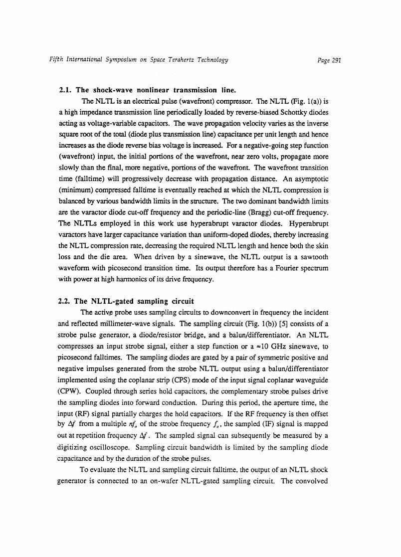
2.1. The shock-wave nonlinear transmission line.
The NLTL is an electrical pulse (wa.vefront) compressor. The NLTL (Fig. 1(a)) is
a high impedance transmission line periodically loaded by reverse-biased Schottky diodesacting as voltage-variable capacitors. The wave propagation velocity varies as the inversesquare root of the total (diode plus transmission line) capacitance per unit length and hence
increases as the diode reverse bias voltage is increased. For a negative-going step function(wavefront) input, the initial portions of the wavefront, near zero volts, propagate more
slowly than the final, more negative, portions of the wavefront. The wavefront transitiontime (falltime) will progressively decrease with propagation distance. An asymptotic
(minimum) compressed falltime is eventually reached at which the NLTL compression is
balanced by various bandwidth limits in the structure. The two dominant bandwidth limits
are the varactor diode cut-off frequency and the periodic-line (Bragg) cut-off frequency.
The NLTLs employed in this work use hyperabrupt varactor diodes. Hyperabrupt
varactors have larger capacitance variation than uniform-doped diodes, thereby increasingthe NLTL compression rate, decreasing the required NUL length and hence both the skin
loss and the die area. When driven by a sinewave, the NLTL output is a sawtooth
waveform with picosecond transition time. Its output therefore has a Fourier spectrumwith power at high harmonics of its drive frequency.
2.2. The NIII-gated sampling circuit
The active probe uses sampling circuits to downconvert in frequency the incident
and reflected millimeter-wave signals. The sampling circuit (Fig. 1.(b)) [5] consists of a
strobe pulse generator, a diode/resistor bridge, and a balunidifferentiator. An NLTL
compresses an input strobe signal, either a step function or a =10 0Hz sinewave, to
picosecond falltimes. The sampling diodes are gated by a pair of symmetric positive and
negative impulses generated from the strobe NLTL, output using a balun/differentiator
implemented using the coplanar strip (CPS) mode of the input signal coplanar waveguide
(CPW). Coupled through series hold capacitors, the complementary strobe pulses drive
the sampling diodes into forward conduction. During this period, the aperture time, the
input (RF) signal partially charges the hold capacitors. If the RF frequency is then offsetby Af from a multiple nf, of the strobe frequency f, , the sampled (IF) signal is mapped
out at repetition frequency Af . The sampled signal can subsequently be measured by a
digitizing oscilloscope. Sampling circuit bandwidth is limited by the sampling diode
capacitance and by the duration of the strobe pulses.
To evaluate the NLTL and sampling circuit falltime, the output of an NLTL shock
generator is connected to an on-wafer NLTL-gated sampling circuit. The convolved

1111111 •
/ I
Ft, 11 TIT MITT ITIIIIIIIITIIITUTIII TI
Measured falltime1.8 ps, 10%-90%
Page 292 Fifth International Symposium on Space Terahertz Technology
(a)
44
MEIa r OutputInput
1\CPW/CPSbalun/differentiator
10NonlinearTransmission Line
Strobe
(b)
(c)
0 5 10 15 20 25 30 35 40Time, ps
Figure 1: (a) NLTL circuit diagram, (b) circuit diagram of an NLTL-gated sampling circuit, and(c) NLTL output measured by an NLTL-gated sampling circuit, both using hyperabrupt diodetechnology.

Fifth International Symposium on Space Terahertz Technology Page 293
responses of sampling circuit and Nun, shock-wave generator is thus measured. With an
NLTL using 1.7 THz exponential hyperabnipt diodes (Fig. 1(c)), a 1.8 ps falltime is
measured. From this, a 1.3 Ps deconvolved NLTL falltime and a 275 GHz sampling
circuit bandwidth are estimated; NUTLs and sampling circuits with approximately twice
this bandwidth have been reported [4,81.
III. The active probesIn commercial sampling oscilloscopes and coaxial-based network analyzers,
connections between the measurement apparatus and the DUTs are provided with coaxial
cables and connectors. 110 GHz coaxial connectors were introduced in March 1993 with
earlier connectors limited to 65 GHz. To obtain broadband measurements beyond this
frequency, we have constructed active probes which place a mm-wave measurement IC in
close proximity to the device under test (DUT). An NWA IC is mounted directly on a
probe with its high-frequency test ports connected to a short low-loss coplanar waveguide
(CPW) quartz probe tip, as shown in Fig. 2. The NWA IC and probe tip are connected by
very short gold ribbon bonds. High-frequency signals (---7-200 Gliz) propagate only on
the probe tip connecting the NWA IC and the DUT. A signal routing substrate provides the
signal paths for the 10-500 kHz LF signals and the 7-14 GHz NLTL, drive signals. With
proper probe tip design, an NLTL-based NWA IC, and low inductance ribbon bonds, the
active probe can attain wider bandwidths than obtainable with instruments using coaxial
connectors. Shakouri et. al. [8] has also reported an active probe for high speed on-wafer
waveform measurements, as opposed to network measurements; in contrast, the work
reported here focuses primarily on network (S-parameter) measurements.
signal routing NVVA integratedsubstrate circuitquartz CPWprobe tip
Figure 2: Active probe hybrid assembly.
Stimulus SignalGenerator Attenuator
DirectionalSampler
DeviceUnder Test
•■■•■■
6-dBAttenuator
Strobe No,
Page 294 Fifth International Symposium on Space Terahertz Technology
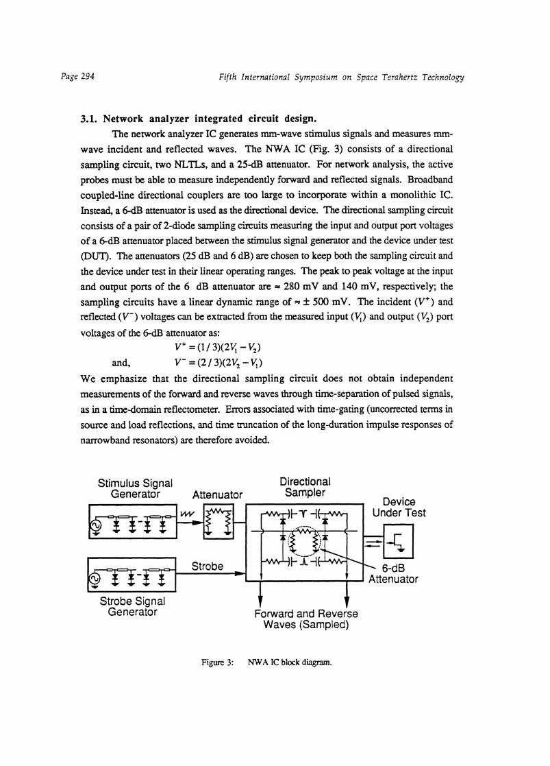
3.1. Network analyzer integrated circuit design.The network analyzer IC generates nun-wave stimulus signals and measures mm-
wave incident and reflected waves. The NWA IC (Fig. 3) consists of a directional
sampling circuit, two NLThs, and a 25-dB attenuator. For network analysis, the activeprobes must be able to measure independently forward and reflected signals. Broadband
coupled-line directional couplers are too large to incorporate within a monolithic IC.
Instead, a 6-dB attenuator is used as the directional device. The directional sampling circuitconsists of a pair of 2-diode sampling circuits measuring the input and output port voltagesof a 6-dB attenuator placed between the stimulus signal generator and the device under test
(DUT). The attenuators (25 dB and 6 dB) are chosen to keep both the sampling circuit and
the device under test in their linear operating ranges. The peak to peak voltage at the input
and output ports of the 6 dB attenuator are 280 mV and 140 mV, respectively; the
sampling circuits have a linear dynamic range of ± 500 mV. The incident (V) andreflected (V- ) voltages can be extracted from the measured input (V) and output (V2) port
voltages of the 6-dB attenuator as:= (1/ 3)(2y— V2)
and, V- = (2 / 3)(2V2
We emphasize that the directional sampling circuit does not obtain independent
measurements of the forward and reverse waves through time-separation of pulsed signals,
as in a time-domain reflectometer. Errors associated with time-gating (uncorrected terms in
source and load reflections, and time truncation of the long-duration impulse responses of
narrowband resonators) are therefore avoided.
Strobe SignalGenerator Forward and Reverse
Waves (Sampled)
Figure 3: NWA IC block diagram.

Fifth International Symposium on Space Terahertz Technology Page 295
In the integrated circuit, one ICLIL generates the strobe pulses which operate the
directional sampling circuit. A second NLTL generates a sawtooth waveform as the
stimulus signal for network analysis. This sawtooth waveform has a 5 V amplitude and a
=2 ps transition time, thus has Fourier components at harmonics of the NL,11 drivefrequency with the spectrum extending from the drive frequency to approximately 200
GHz. A 7-200 GHz frequency coverage is not readily obtained with the swept-frequencysources used in commercial network analyzers. The stimulus signal is attenuated by anattenuator to levels suitable for linear characterization of transistor circuits, and is passedthrough the directional sampling circuit to the MIT. IC fabrication is described in [71.
3.2. Probe tip design.
The CPW probe tip limits the probe bandwidth, hence its design is critical. Probe
tips in commercial microwave wafer probes are long (=1.5 cm) and are fabricated onalumina (e=9 8) substrate. Consequently, these have large attenuation above 65 GHz.
Signal attenuation on the CPW probe tips arises from skin and radiation losses. For a
given line impedance, skin loss is [9]:
-Vnisl-toI aV(1+ er ) 12 otshia
=
4/70d1C(k)K(k11—(wId)}( 4;rw(I —wldr rc2d [ +2 4-+ in
t(14-wid)w
t4ird(1— w/ d).1t(l+wid)
where f is the frequency in Hz, er the substrate dielectric constant, d the CPW ground-ground spacing, w the center conductor width, t the metal thickness, p o the permeability
of vacuum, cr the metal (gold) conductivity, ri0 =377 CI the free space impedance,k=wId, =
K and K(k) the complete elliptic integral of first order. Radiation loss
is [U]:
rc \ ,5 ery f3d2
arad z--* r-- 2j -v2V1+ Er cl((k)K(Ici)
where c is the speed of light. The total attenuation is then:a 041 = ash„ arad
Consequently, with appropriate scaling of line dimensions, CPWs on substrates with lower
Er can attain lower attenuation. Further, for a given substrate, d can be chosen such thatectoki, is minimized at a particular frequency. Shown in Fig. 4 are the computed attenuation-
frequency characteristics of CPW of different dimensions on alumina (e r =9.8) and on
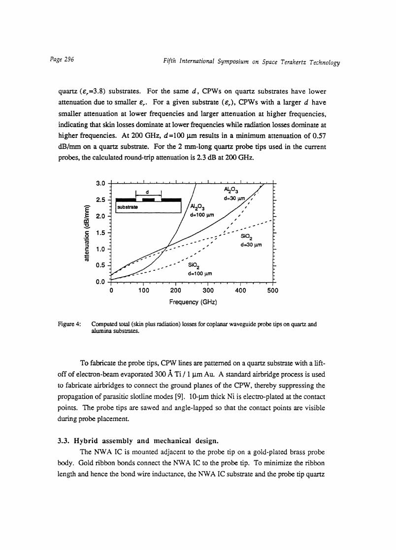
Page 296 Fifth International Symposium on Space Terahertz Technology
quartz (er=3.8) substrates. For the same d, CPWs on quartz substrates have lower
attenuation due to smaller er • For a given substrate (er), CPWs with a larger d have
smaller attenuation at lower frequencies and larger attenuation at higher frequencies,
indicating that skin losses dominate at lower frequencies while radiation losses dominate at
higher frequencies. At 200 GHz, d=100 gm results in a minimum attenuation of 0.57
dB/mm on a quartz substrate. For the 2 mm-long quartz probe tips used in the current
probes, the calculated round-trip attenuation is 2.3 dB at 200 GHz.
100 200 300 400 500
Frequency (GHz)
Figure 4: Computed total (skin plus radiation) losses for coplanar waveguide probe tips on quartz andalumina substrates.
To fabricate the probe tips, CPW lines are patterned on a quartz substrate with a lift-
off of electron-beam evaporated 300 A Ti / 1 gm Au. A standard airbridge process is used
to fabricate airbridges to connect the ground planes of the CPW, thereby suppressing the
propagation of parasitic slotline modes [9]. 10-gm thick Ni is electro-plated at the contact
points. The probe tips are sawed and angle-lapped so that the contact points are visible
during probe placement.
3.3. Hybrid assembly and mechanical design.
The NWA IC is mounted adjacent to the probe tip on a gold-plated brass probe
body. Gold ribbon bonds connect the NVJA IC to the probe tip. To minimize the ribbon
length and hence the bond wire inductance, the NWA IC substrate and the probe tip quartz

Fifth International Symposium on Space Terahertz Technology Page 297
substrate have the same 20 mil thickness. The inductance of gold ribbon of thickness t,
width w, and length I can be calculated as [111:
L 2
5.08 x 1O-3 /[ n(--1---) +1.19 + 0.22 x(- nil/ •w+ t)
So for our tx w x1=0.25 mil x 2 mil x 4 mil ribbons, L=40 pH. The circuit includes one
bond in the center (signal) conductor and two parallel bonds for the ground connection,
hence the total inductance of the ribbon bonds is 60 pH (1.5x L). The calculated 60 pH
bond inductance was experimentally verified by using the NWA IC to measure the
magnitude of the reflection from the wire bond. The ribbon connection limits the probebandwidth to 1000 I (2 7t. • 60 pH) =265 GHz.
Because the probe tips are very short (2 mm), they do not flex when the probe is
brought into contact with the DUT. Instead, the necessary mechanical flexure for reliableprobe-DUT contacts is provided through elastic materials (i.e. a rubber joint) placed at the
interface between the probe and its supporting a m
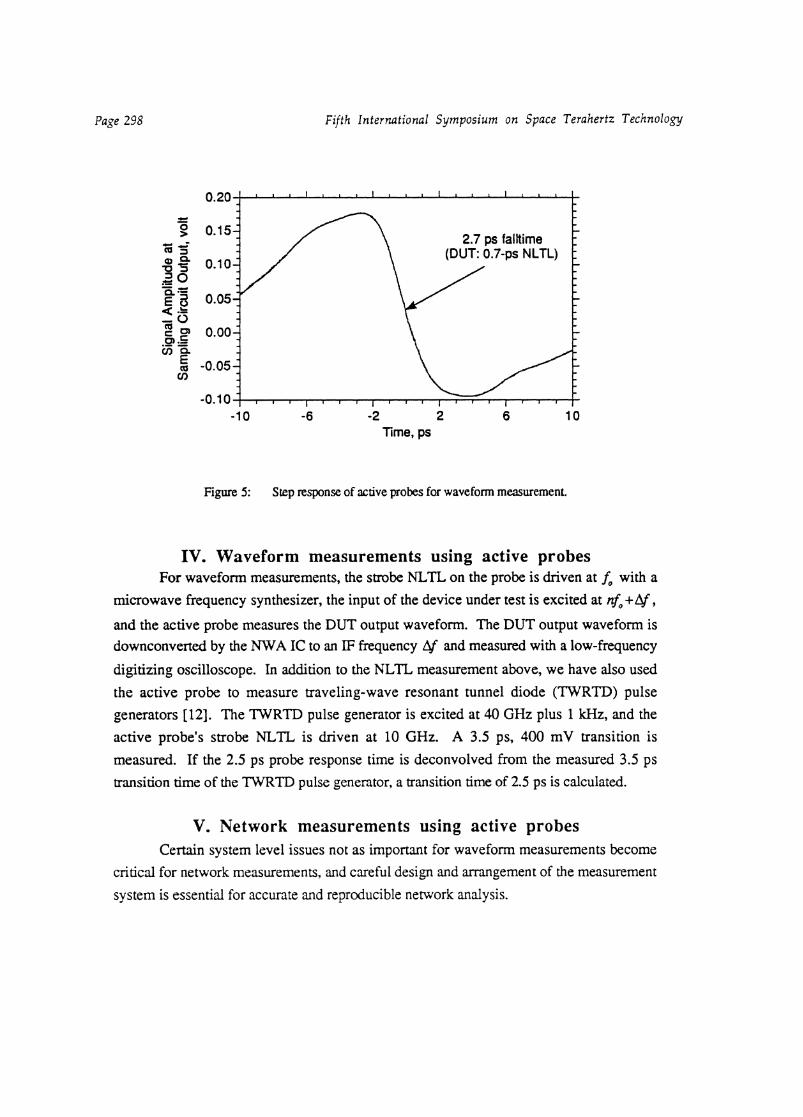
3.4. Active probe bandwidth measurement.
When the active probes are used for waveform measurements, the bandwidth (13W)
of the probes can be determined by falltime measurements with the probes measuring
signals which have much smaller falltimes than that of the probes. In contrast, when theactive probes are used for network measurements, the stimulus signal for the DUT is
supplied through the probes, thus the probe falltime measurements should include the
contribution from the probe's NLTL stimulus signal generator. Fig. 5 shows the stepresponse of the active probes with the probes measuring an NLTL, with a 0.7 Ps falltime
[4]. If the measured 2.7 ps is deconvolved from the 0.7 ps input signal falltime, a probe
falltime of 2.6 Ps is estimated, corresponding to a probe -3-dB bandwidth of 135 GHz for
waveform measurements. To determine the uncorrected (pre-calibration) bandwidth of the
active probe for network measurements, we measured the falltime of the reflection from an
open circuit load with the active probe providing its own stimulus signal. The measured 3
ps reflection falltime, corresponding to an active probe -3-dB BW of 110 GHz for networkmeasurements, includes the convolved contributions of the NLTL pulse generator falltime,
the capacitance charging time of the two sampling circuits, the probe tip losses, and the
inductance of bond wires connecting the probe tip to the NWA IC. As with conventionalVNAs, measurements can be obtained significantly beyond the uncorrected -3-dB BW after
calibration.
2.7 Ps falltime(DUT: 0.7-ps NLTL)457
v• 0.10—°
E a 0.05—<
0coc 0.00—o) .c'co a
cts -0.05 —
106-2 2"Time, ps
0.20
-0.10 I =-10 -6
I I I
Page 298 Fifth International Symposium on Space Terahertz Technology
Figure 5: Step response of active probes for waveform measurement
IV. Waveform measurements using active probesFor waveform measurements, the strobe NLTL on the probe is driven at fo with a
microwave frequency synthesizer, the input of the device under test is excited at nfo + f
and the active probe measures the DUT output waveform. The DUT output waveform is
downconverted by the NWA IC to an IF frequency if and measured with a low-frequency
digitizing oscilloscope. In addition to the NUL measurement above, we have also used
the active probe to measure traveling-wave resonant tunnel diode (TWRTD) pulse
generators [121 The TWRTD pulse generator is excited at 40 GHz plus 1 kHz, and the
active probe's strobe NUTI., is driven at 10 GHz. A 3.5 ps, 400 mV transition is
measured. If the 2.5 ps probe response time is deconvolved from the measured 3.5 ps
transition time of the TWRTD pulse generator, a transition time of 2.5 Ps is calculated.
V. Network measurements using active probesCertain system level issues not as important for waveform measurements become
critical for network measurements, and careful design and arrangement of the measurement
system is essential for accurate and reproducible network analysis.
active probe7-14 GHzNLTL drive signals
stimulus
differencecircuit
IF signal processing electronics
Jbuffers
downconvertedforward & reverse
waves (10-500 kHz)
7-200 GHzsignals
deviceunder test
V'.(1/3)(2V1-V)
ra(2/3)(2V2-V1)
digitizing scope
Fifth International Symposium on Space Terahertz Technology Page 299
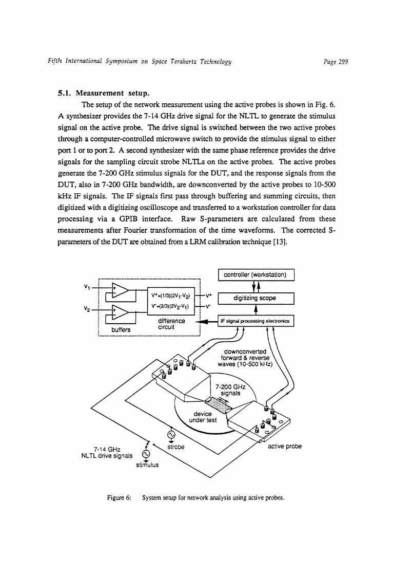
5.1. Measurement setup.
The setup of the network measurement using the active probes is shown in Fig. 6.A synthesizer provides the 744 GHz drive signal for the NLTL to generate the stimulus
signal on the active probe. The drive signal is switched between the two active probesthrough a computer-controlled microwave switch to provide the stimulus signal to either
port 1 or to port 2. A second synthesizer with the same phase reference provides the drivesignals for the sampling circuit strobe NULs on the active probes. The active probesgenerate the 7-200 GHz stimulus signals for the DIJT, and the response signals from the
DUT, also in 7-200 GHz bandwidth, are downconverted by the active probes to 10-500kHz IF signals. The IF signals first pass through buffering and summing circuits, then
digitized with a digitizing oscilloscope and transferred to a workstation controller for dataprocessing via a GPIB interface. Raw S-parameters are calculated from thesemeasurements after Fourier transformation of the time waveforms. The corrected S-
parameters of the DUT are obtained from a LRIVI calibration technique [131
controller (workstation)
Figure 6: System setup for network analysis using active probes.

Page 300 Fifth International Symposium on Space Terahertz Technology
Since the active probes function correctly over a stimulus drive frequency range of7-14 GHz, a complete octave in frequency, S-parameter measurements are possible over
the entire frequency spectrum from 7-200 GHz. The LRM calibration was performed
using the Cascade Microtech calibration standards consisting of a 1 Ps through line, a 50 Cimatch load, and a short circuit [14].
5.2. Measurement bandwidth, accuracy, and reproducibility.
As distinct from the -3 dB bandwidth of an electronic device or circuit, the
bandwidth of a network analyzer is defined by the required accuracy and by themeasurement reproducibility. There are five major limitations to the network measurement
accuracy and reproducibility.
The first limitation arises from the two microwave synthesizers used to drive the
NLTL strobe and stimulus signal generators on the active probes. Although the twosynthesizers share a common 10 MHz frequency standard, they have significant relativephase fluctuations. These phase fluctuations produce phase noise sidebands about each
harmonic of the RF fundamental frequency [151 As illustrated in Fig. 7, sampling of theRF signals (at fo and its harmonics) downconverts the RF signal spectrum (Fig. 7(a)) to
much lower IF frequencies (if and its harmonics). Depending on the bandwidth of the
phase noise sidebands and the IF fundamental frequency, significant overlap of phase noise
sidebands can occur (Fig. 7(b)). Therefore, a given Fourier component of the RF signal is
detected against a noise background set by the collective phase modulation sidebands of all
other Fourier components. To reduce this effect, the IF fundamental frequency should be
larger than the phase noise bandwidth(Fig. 7(c)). We have measured the synthesizer
single-sideband phase noise spectral density in unit of dBc (1 Hz). We emphasize that thephase noise spectral density is the relative phase noise measured with the synthesizers
operating from the same crystal oscillator fundamental frequency reference, which is the
relevant quantity. The phase noise is significant (= -80 dBc per Hz) at frequencies close to
the carrier frequency, and phase modulation due to power line harmonics contributes large
phase noise components at 60 Hz and its first several harmonics. The phase noisespectrum decreases rapidly for f >10 kHz (< -95 dBc per Hz) , therefore IF frequencies ifof >10 kHz should be used. The mm-wave signal at nfo is downconverted by the probe to
an IF frequency '4c , and nAf must therefore be less than the IF port bandwidth. The
probe IF output impedance is high (=MO 1(0) and the IF signal bandwidth is limited by
capacitance of cables connecting the active probes to the digitizing oscilloscope. To obtaina >500 kHz IF signal bandwidth (necessary for >10 kHz IF fundamental frequencies), an

Fifth International Symposium on Space Terahertz Technology Page 301
Frequency
A
Frequency (expanded scale)
Frequency (expanded scale)
a)
c)
Figure 7: Phase noise sideband overlap due to downconversion of frequency spectrum by the samplingcircuits: (a) spectrum at the input of the sampling circuit with RF fundamental frequencyfo ,
(b) spectrum at the output of the sampling circuit with IF fundamental frequency Af , and (c)
spectrum at the output of the sampling circuit with IT fundamental frequency 4j .' where
>

Page 302 Fifth International Symposium on Space Terahertz Technology
IF buffer circuit (Fig. 6) is mounted close to the active probe on the probe arm therebyreducing the interconnecting cable length (hence parasitic capacitance).
The second limitation arises from the 8-bit digitizing oscilloscope. During dataacquisition, the IF waveform is digitized with 8-bit resolution. Since the stimulus(incident) time waveforms are approximately sawtooth waveforms, their spectral content
decreases as 1/ nn (normalized to the peak to peak amplitude of the time waveform), where
n is the nth harmonic of the fundamental frequency, hence the resolution for signal at
higher frequencies are much less than 8-bit, severely limiting the accuracy, directivity, and
dynamic range of the VNA at higher frequencies. For a waveform at 8 GHz fundamental
drive frequency, for example, the signal amplitude at 200 GHz (25 th harmonic) is 1 / 25x,corresponding to a signal/quantization error ratio of 21 dB at 200 GHz. Because the NWAIC measures the sum of the incident and reflected signals, the quantization error becomes
particularly severe when measuring reflections from DUTs with =50 LI impedance where
the small reflected signal is much smaller in magnitude than the large incident signal.. Toimprove the system directivity, the approximate incident and reflected signals are obtained
by a difference circuit (Fig. 6) before data acquisition by the digitizing oscilloscope. The
sampling circuits also contribute noise to the network measurements. The measured noise
figure of the sampling circuits is 65 dB [151. Despite the high noise figure, the sampling
circuit noise is negligible compared to the quantization error and phase noise.The third limitation is due to the LRM calibration standards. In the LRIVI calibration
technique, the transmission matrices of the 1 Ps through line and the 50 C2 match load mustbe accurately defined while that of the reflect standard (with reflection coefficient of =,1)
needs only be known approximately. The 1 Ps CPW through line is defined as a lossless,
clispersionless transmission line, which is still a good approximation to 200 GHz. For
higher frequencies, the non-ideality must be incorporated into the model for the 1 Ps
through line. The 50 standard is modeled as a perfect 50 fl in series with a variable
inductor whose inductance depends on the amount of probe-standard overlap {161 This
model is not verified beyond 110 GHz. Use of offset calibration standards and offset
DUTs results in similar probe to calibration standard/DUT launching characteristics andmay improve calibration standard (hence measurement) accuracy [17].
The fourth limitation is due to crosstalk/isolation between the active probes.
Currently, the NWA ICs and the probe tips on the active probes are exposed to air. When
two probes are brought within 200 gm of each other, some degree of electromagnetic
coupling is observed. The probe crosstalk cannot be eliminated by calibration because themagnitude of the coupling depends upon probe placement. Better shielding of the NWA
ICs and probe tips should reduce this effect.
Fifth International Symposium on Space Terahertz Technology Page 303
Finally, the network measurement bandwidth is ultimately limited by the active
probe bandwidth as the mm-wave signals are attenuated beyond the -3 dB bandwidth of the
active probe. The bandwidth limits of the active probes arise from the NWA ICs, the probe
tips, and the interconnection between the ICs and the tips. The current NWA ICs use 275
GHz-bandwidth sampling circuits and 1.8 Ps NLThs. 515 Gliz bandwidth sampling
circuits and 0.68 Ps NLTLs have been fabricated [4]; using these, the NWA IC bandwidth
can be extended to at least 400 GHz. The bandwidth of the active probes would then be
limited by the probe tips and the interconnection bandwidth, currently 260 Gliz. Probe tip
losses and bond inductances can be reduced through use of beam lead technology to mount
NWA ICs close to probe tips, thereby minimizing both the CPW probe tip length and
eliminating bond wire inductance.
We emphasize that the network measurement bandwidth is not the same as the -3
dB bandwidth of the active probes. Instead, the network measurement bandwidth is
limited by the collective contribution of all the factors describe above.
5.3. Measurement results.
To verify the repeatability of the vector network analyzer (VNA), the VNA was
calibrated and the 1-ps through line calibration standard was subsequently remeasured.
The measured and calculated S-parameters are shown in Fig. 8. Two measurements were
performed 30 minutes apart with the same calibration. As shown in Fig. 8(a), the
reproducibility in transmission measurement is within -±0.3 dB to 160 GHz, and degrade to
±1 dB around 200 GHz; the phase repeatability, also shown in Fig. 8(a), is within 0.1 Ps
to 200 Mr, the return loss, shown in Fig. 8(b), is less than -30 dB to 160 GHz, and
becomes -10 dB around 200 GHz. Measurements of the 50 CI plus 7.5 pH calibration
standard show only small deviations from the expected characteristics from 7 to 150 GHz,
showing larger deviations between 150 GHz and 200 GI12 because of the reduced system
directivity, as is also apparent in the measurements of the 1-ps through line (Fig. 8).
However, when the probes are raised (open circuit termination), the measured S-
parameters (not shown) have as much as 1 dB error above 100 GHz. While measurement
reproducibility is limited by phase noise, quantization errors, and probe crosstalk,
measurement accuracy includes the effect of errors in the calibration standards. S-
parameter measurements of the calibration standards themselves give good indications
about system reproducibility (hence system phase noise, quantization errors, and probe
coupling) regardless the correctness of the models for the calibration standards. Therefore,
because less accurate measurements are obtained for an open circuit load than for the 1-ps

1
-40 60 120 160 200
Fnoquertcy,GP
(b)
-20:
-60:
$ 0
2
0
•1
-2
-3 4,
-4
45
-0
:
-45
: 1• • . . -90
40 BO 120 160 200Frogpincy,GHz
(a)
-50
Page 304 Fifth International Symposium on Space Terahertz Technology
through line (a pre-defined standard), errors in the calibration standards themselves are
currently the dominant source of measurement error.
Figure 8: 2-port S-parameter measurements (taken at 30 minutes time intervals) of a 1-ps through linecalibration standard: (a) magnitude and phase of S21, and (b) magnitude of S11.
With this VNA, we measured 2 MIMICs fabricated with a 0.16 pm pseudomorphic
MODFET technology. The S-parameters were obtained with NLTL drive frequencies
varied from 7 to 9 GHz in 0.2 GHz steps, hence the resulting measured data points were at
these drive frequencies and their harmonics. For measurements at any other frequencies in
the 7-200 GHz range, appropriate NLTL &lye frequencies can always be chosen so that
these frequencies of interest are covered by certain harmonics of the selected NLTL drive
frequencies. The first MMIC is a 5-stage traveling-wave amplifier (TWA) [18,19]. Fig. 9
shows the gain and return losses of the TWA measured by the active probes. The gain of
the TWA is typically 8 dB over the full 7-80 GHz band, and drops off rapidly beyond 80
GHz; the input and output matching is better than -5 dB over the full 7-80 GHz. S-
parameter measurements of the LNA were also performed on a similar LNA chip with a
commercial coaxial 50 GHz network analyzer extended to 78 GHz by a waveguide test set
[201. The second MMIC is a medium power amplifier (MPA) that is designed to provide
gain from 60-80 GHz. Fig. 10 shows the gain and return losses of the MPA measured by
the active probes and by the commercial network analyzer. The MPA has more than 8 dB
gain in the 60-80 GHz band, and, as measured by the active probes, the gain is greater than
5 dB to 90 GHz; the return losses are better than -8 dB in the 65-85 GHz band. Both
amplifiers were susceptible to radio-frequency bias-circuit oscillations during
measurements, oscillations which could be suppressed by small adjustments of the circuit
DC bias voltages. Consequently, the MMIC bias conditions during measurements with the

(b)
30 • 'who preibe
20 ": Ssio
80 100
1 0 •
20 40 60Frequency. GHZ
(a)
151
OF
Active Probe---- 5610
060 70 810
Frequency, GHz
(a)
t•Ci.tI3
20=
20=
40 60Ftyquoncy, GHz
(b)
500
30100
10 30
- 20
Fifth International Symposium on Space Terahertz Technology Page 305
commercial network analyzer were slightly different from those used during measurements
with the active probes.
Figure 9: S-parameter measurements of a 5-stage traveling-wave amplifier: (a) gain, and (b) returnlosses.
Figure 10: S-parameter measurements of a medium power amplifier. (a) gain, and (b) return losses.
As is apparent from these MMIC S-parameter measurements, good agreement
between those measured by the active probes and by the commercial network analyzer is
obtained in the 7-80 GHz band. Discrepancies between these measurements may be due to
instrument errors, differences in circuit bias conditions, and circuit-circuit variations across
the wafer. Beyond 80 GHz, the MMIC can only be measured by the active probes (we do
not have access to a commercial 75-110 GHz network analyzer).

Page 306 Fifth International Symposium on Space Terahertz Technology
V. ConclusionCommercial sampling scopes and network analyzers bandwidths are limited to 120
GHz, significantly below the state-of-the-art transistor and MMIC bandwidths. WithNLTL technology, we have fabricated active probes incorporating GaAs NWA ICs andlow loss, rugged quartz probe tips. Using the active probes, we have measured
waveforms with 2.5 ps transition times, and we have demonstrated, with measurement of a
1-Ps through line, a VNA with ±0.3 dB reproducibility and better than 30 dB correcteddirectivity to 160 GHz, and with ±1 dB reproducibility and better than 10 dB corrected
directivity to 200 GHz. With this VNA, we have characterized 3 MMICs, and the S-
parameters show good agreement with those measured by a commercial network analyzer
from 7-78 GHz. The active probes are convenient tools for broadband on-wafercharacterization of transistors and MMICs. With improvement in calibration standards,
quantization errors, microwave synthesizer noise, probe crosstalk, and active probe
bandwidths, more accurate and reproducible network analysis beyond 200 GHz is
possible.
Acknowledgment: This work was supported by an AFOSR grant (grant number;F49620-92-J-0469), an AFOSR/AASERT grant (grant number: F49620-92-J-0365), an
NSF Presidential Young Investigator Award, and a California/Hughes Micro contract. We
are grateful to Dr. P. Tasker, Dr. M. Schlechtweg, and Dr. J. Braunstein at Fraunhofer
Institute for supply of the MMICs.
References:{1] U. K. Mishra, A. S. Brown, and S. E. Rosenbaum, "DC and RF performance of 0.1
1.1m gate length AllnAs-GalnAs pseudo-morphic HEIVITs", Technical Digest, 1988
International Electron Device Meeting, Dec. 4-11, San Francisco.
[2] R. Majidi-Ahy, C. Nishimoto, M. Riaziat, M. Glenn, S. Silverman, S. Weng, Y.
Pao, G. Zdasiuk, S. Bandy and Z. Tan, "100 GHz High-Gain InP MMIC Cascode
Amplifier", 1990 GaAs IC Symposium, Oct. 7-10, New Orleans.
[31 M. J. W. Rodwell, M. Kamegawa, R. Yu, M. Case, E. Carman, and K. S. Kiboney,"GaAs Nonlinear Transmission Lines for Picosecond Pulse Generation and
Millimeter-Wave Sampling", IEEE Trans. on Microwave Theory and Techniques,
Vol. 39, No.7, July 1991.
[4] S. T. Allen, U. Bhattacharya, and M. J. W. Rodwell, "4 THz sidewall-etchedvaractors for sub-mm-wave sampling circuits," Technical Digest, 1993 GaAs IC
Symposium, Oct. 10-13, San Jose.
Fifth International Symposium on Space Terahertz Technology Page 307
[5] R. Y. Yu, M. Case, M. Kamegawa, M. Sundaram, M. J. W. Rodwell, and A. W.Gossard, "275 GHz 3-mask integrated GaAs sampling circuit," Electronics Lett.,
vol. 26, No. 13, June 21, 1990, pp. 949-951.
[6] R. A. Marsland, V. Valdivia, C. J. Madden, M. J. W. Rodwell, and D. M. Bloom,"Monolithic integrated circuits for rnillimeter-wave instrumentation," Technical
Digest, 1990 GaAs IC Symposium, Oct. 740, New Orleans.
[7] R. Y. Yu, M. Kamegawa, M. Case, M. J. W. Rodwell, and J. Franklin, "A 2.3-ps
time-domain reflectometer for millimeter-wave network analysis," IEEE Microwaveand Guided Wave Lett., vol. 1, no. 11, Nov. 1991, pp. 334-336.
[8] M. S. Shakouri, A. Black, B. A. Auld, and D. M. Bloom, "500 GHz MMIC
sampling wafer probe," Electronic Letters, vol. 29, no. 6, pp. 557-558, March 18,
1993.[9] R. K. Hoffmann, "Handbook of microwave integrated circuits," Artech House Inc.,
1987.[10] D. B. Rutledge, D. P. Neikirk, and D. P. Kasilingarn, "Integrated-Circuit Antennas"
in Infrared and Millimeter Waves, Ed. by K. J. Button, Vol. 10, pp. 1-90, New York:
Academic Press, 1984
[11]M. Caulton, "Lumped elements in microwave integrated circuits," in Advances in
Microwaves, Ed. by Leo Young and R Sobol, , pp. 143-167, Academic Press, 1974
[12] R. Y. Yu, Y. Konishi, S. Allen, M. Reddy, and M. J. W. Roclwell, "A traveling-
wave resonant tunnel diode pulse generator," submitted to Microwave and GuideWave Lett. for publication.
[13]H. J. Eui and B. Schiek, ""Thru-Match-Reflect. One Result of A Rigorous Theory
for De-embedding and Network Analyzer Calibration," Proceedings of the 18th
European Microwave Conference, Stockholm, Sweden, 1988.
[141 Specification Sheet for Calibration Kit 25, Cascade Microtech, Inc., PO Box 1589,
Beaverton, OR, 97075-1589.
[15] Y. Konishi, M. Karnegawa, M. Case, R. Yu, S. Allen, and M. J. W. Rodwell, "A
broadband free-space millimeter-wave vector transmission measurement system," to
be published in IEFE Transactions on Microwave Theory and Techniques.
[16]A. Davidson, K. Jones, and E. Strid, "LRM and LRR.M calibrations with automatic
determination of load inductance", Application Note, Cascade Microtech, 14255 SW
Brigadoon Ct., Beaverton, OR 97005.
[17] S. M. J. Liu, K. H. G. Duh, S. C. Wang, O. S. A. Tang, and P. M. Smith, "75-110GHz InGaAs/GaAs HEMT high gain MMIC amplifier", Tech. Digest, GaAs IC
Symposium, San Jose, Oct. 10-13, 1993.

Page 308 Fifth International Symposium on Space Terahertz Technology
[18] M. Schlechtweg, P. Tasker, W. Reinert, J. Braunstein, W. Haydi., A. Hulsmann, andK. Kohler, "High gain 70-80 GHz MA/11C amplifiers in coplanar waveguide
technology," Electronics Lett., vol. 29, no. 12, June 1993, pp. 11194120.[19] J. Braunstein, M. Schlechtweg, P. J. Tasker, W. Reinert, A. Julsmann, K. Kohler,
W. Bronner, R. Bosch, and W. Haydl, "High performance narrow and wide
bandwidth amplifiers in CPW-technology up to W-band," Technical Digest, 1993GaAs IC Symposium, Oct. 10-13, San Jose.
[20] P. J. Tasker, M. Schlechtweg, and J. Braunstein, "On-wafer single contact S-
parameter measurements to 75 GHz: calibration and measurement system," 23rd
European Microwave Conf., Madrid, 1993