Self Learning Material Microprocessors and
Microcontrollers (BSBC-402)
Course: Bachelor of Computer Applications
Semester-IV
Distance Education Programme
I.K. Gujral Punjab Technical University
Jalandhar
Syllabus I.K. Gujral Punjab Technical University Scheme of (BSBC)
Batch 2015 onwards
BSBC 402 Microprocessors and Microcontrollers
SECTION-A
Introduction to Microprocessors: Historical Background of Microprocessors, Applications of
Microprocessors, Introduction to 8085, Architecture of 8085, Pin Diagram of 8085.
SECTION-B
Instruction Cycle, Timing Diagrams of Memory Read/Write Operations &timing diagrams of
various Instructions, Addressing Modes, Instruction Set, Data Transfer Instructions, Arithmetic
Instructions, Logical Instructions, Branch Instructions, Control Instructions, RISC &CISC
Processors.
SECTION-C
Introduction to Microcontrollers: Architecture of Microcontroller, Microcontroller Resources,
Resources in Advanced and Next Generation Microcontroller, 8051 Microcontroller, Internal and
External Memories, ROM Based Controller, Counters and Timers, Synchronous Serial and
Asynchronous Serial Communication, Interrupts.
SECTION-D
Peripheral Devices and Controllers: Introduction and Architecture of DMA Controller8257,
Architecture of Programmable Interrupt Controller 8259, Clock Generator, Architectureof8284.
Suggested Books:
1. Microprocessor Architecture, Programming and Applications with 8085, Ramesh. S. Gaonkar,
Fourth Edition, Penram International Publishing
2. 8051 Microcontroller and Embedded Systems, Muhammad Ali Mazidi Janice Gillispie Mazidi,
Second Edition, PHI
3. Fundamentals of Microprocessors and Microcomputers, B. Ram, Fourth Edition, Dhanpat Rai
Publications
4. The Intel Microprocessors 8086/8088,80186/80188, 80286, 80386, 80486, Pentium Pro
Architecture, Programming and Interfacing, B. Brey, Fifth Edition, Prentice Hall International
1
Table of Contents
Lesson No
Title Author details Page No.
1 Introduction to Microprocessor and its Applications
Rekha Devi,Assistant
Professor CDAC, Mohali
1
2 Introduction to 8085 Architecture Rekha Devi, Assistant
Professor CDAC, Mohali
16
3 Instruction Set 8085 Mr. Satbir Singh Project
Engineer, C-DAC Mohali
36
4 Addressing Mode Mr. Satbir Singh Project
Engineer, C-DAC Mohali
63
5 8085 Instruction Timing Mr. Satbir Singh Project
Engineer, C-DAC Mohali
74
6 Introduction to Microcontroller Rekha Devi, Assistant
Professor CDAC, Mohali
92
7 Introduction to Microcontroller 8051 Dr. Balwinder Singh
Assistant Professor
C-DAC Mohali
117
8 Programming and Interfacing with 8051 Microcontroller
Dr. Balwinder Singh
Assistant Professor
C-DAC Mohali
138
9 Counters, Timers and Interrupts Dr. Balwinder Singh
Assistant Professor
C-DAC Mohali
160
10 Introduction to DMA Controller 8257 Architecture
Anurag, Project Associate
CDAC, Mohali
194
11 Introduction to Programmable Interrupt Controller 8259 Architecture
Anurag, Project Associate
CDAC, Mohali
211
12 Introduction to Clock Generator 8284 Architecture
Anurag, Project Associate
CDAC, Mohali
229
Reviewed by: Dr. Dalveer Kaur, Assistant Professor, ECE
Punjab Technical University, Kapurthala
© IK Gujral Punjab Technical University Jalandhar
All rights reserved with IK Gujral Punjab Technical University Jalandhar
1
Chapter 1: Introduction to Microprocessors and its Applications
Structure
1.0 Objectives
1.1 Introduction to Microprocessor
1.1.1 Description of Basic Microprocessor
1.1.2 Classification of computers
1.2 Evolution of Microprocessor
1.3 Applications of Microprocessor:
1.0 Objectives
After studying this chapter you will understand
Basics of Microprocessor
Classification of computers
Students will understand the History of Microprocessor
Many applications of microprocessors are explained in the last section of the
chapter
1.1 Introduction
A Microprocessor is a semiconductor device that can includes the arithmetic Logic
Unit(ALU) ,registers and a control unit on a single chip. It also called as Brain of the
processing unit that process the digital data. It communicate in binary numbers ‘0’ or ‘1’
called bits . It is a computer processor that incorporated the central Processing Unit’s
(CPU) functions on a single chip or integrated circuits(ICs) . it reads the binary
instructions from a Memory device and accepts binary data as input and process data
according to the instruction given to the processor and computes the results as output. So
Microprocessor is a programmable device which processes only the digital data, and
widely used in the May applications , like Automation control, Consumer electronics,
Defense applications etc.
Computer is devices which receives the input data and compute the results according to
the instructions given in the program. A block diagram of a digital microcomputer is
given in fig 1. The CPU is the heart of the computer which controls the every device. The
computer which is works based on a microprocessor is called a microcomputer. A
microcomputer system includes a CPU (microprocessor), memory elements like ROM &
RAM and I/O devices. The data bus and address (control) buses is used to connect the
I/O devices and memory with the processor . The CPU entertains only one peripheral
device at a time by enabling the peripheral by the control signal. If we want to send data
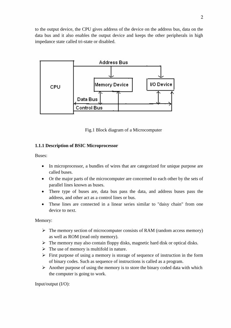
2
to the output device, the CPU gives address of the device on the address bus, data on the
data bus and it also enables the output device and keeps the other peripherals in high
impedance state called tri-state or disabled.
Fig.1 Block diagram of a Microcomputer
1.1.1 Description of BSIC Microprocessor
Buses:
In microprocessor, a bundles of wires that are categorized for unique purpose are
called buses.
Or the major parts of the microcomputer are concerned to each other by the sets of
parallel lines known as buses.
There type of buses are, data bus pass the data, and address buses pass the
address, and other act as a control lines or bus.
These lines are connected in a linear series similar to "daisy chain" from one
device to next.
Memory:
The memory section of microcomputer consists of RAM (random access memory)
as well as ROM (read only memory).
The memory may also contain floppy disks, magnetic hard disk or optical disks.
The use of memory is multifold in nature.
First purpose of using a memory is storage of sequence of instruction in the form
of binary codes. Such as sequence of instructions is called as a program.
Another purpose of using the memory is to store the binary coded data with which
the computer is going to work.
Input/output (I/O):
3
The input/ output section consist of an input device and output device and input
/output ports.
The I/O section enables the computer to take the data from the user and/or send
the data to the outside world.
Devices such as keyboards, video display terminals, printers and modems are
called as peripherals and they are connected to the I/O section. Peripherals
establish communication between the user and computer.
Ports:
The actual physical devices which are used for interfacing the computer buses
with the external systems are called as ports.
The ports are of two types namely input ports and output ports.
The input port will allow the connection of data from the keyboard or an A/D
converter or some other source to the computer.
The computer actually reads the information connected through the input ports.
Such a reading takes place under the control of the CPU.
An output is used for connecting the data from the computer to the outside world.
The processed data is sent from the computer to a peripheral such as a video
terminal, or a printer or a D/A converter.
Practically the simplest type of an I/O port is a set of parallel D flip-flops. When
used an input port the D inputs are connected to the peripherals and Outputs are
connected to the data bus of computer.
When used as output port the D inputs are connected to data bus abd Q outputs to
the peripheral devices.
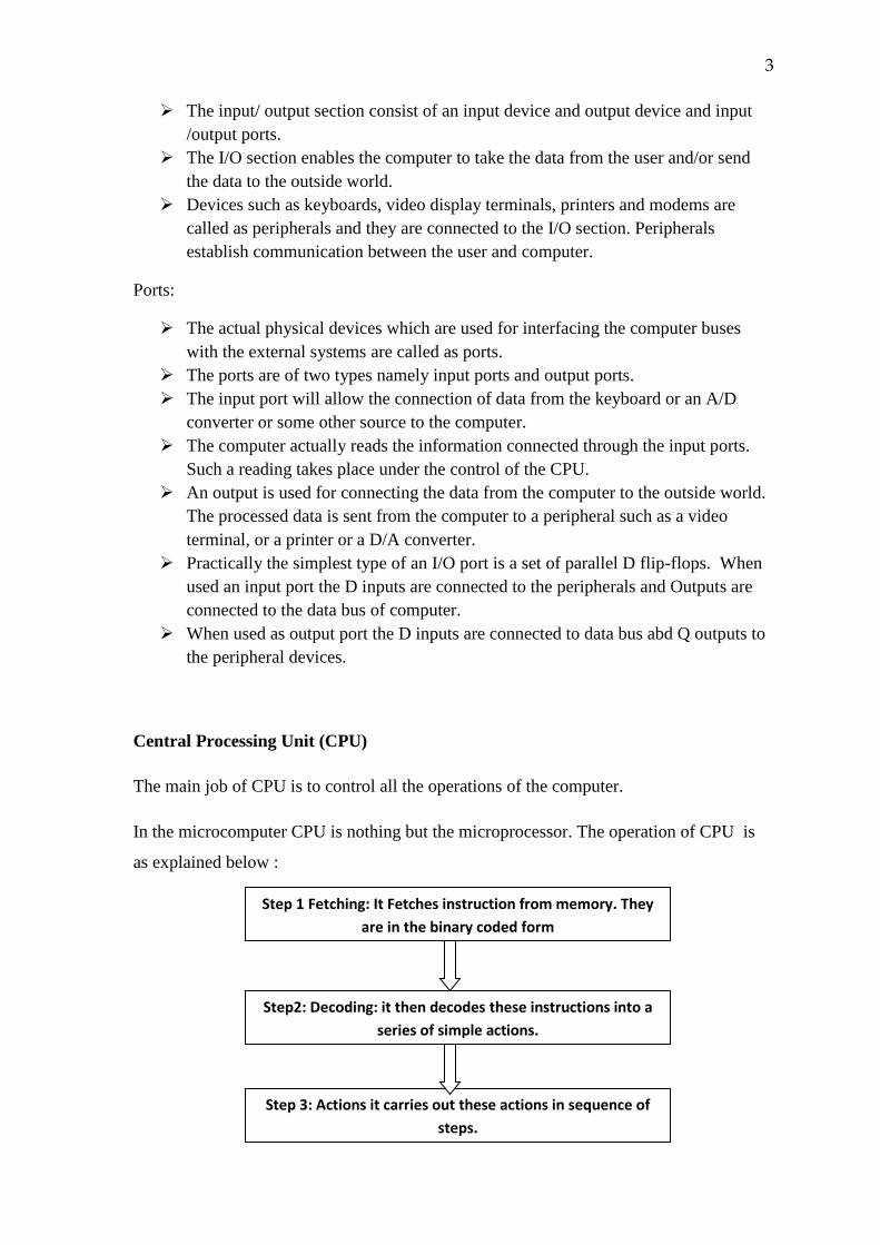
Central Processing Unit (CPU)
The main job of CPU is to control all the operations of the computer.
In the microcomputer CPU is nothing but the microprocessor. The operation of CPU is
as explained below :
Step 1 Fetching: It Fetches instruction from memory. They
are in the binary coded form
Step2: Decoding: it then decodes these instructions into a
series of simple actions.
Step 3: Actions it carries out these actions in sequence of
steps.
4
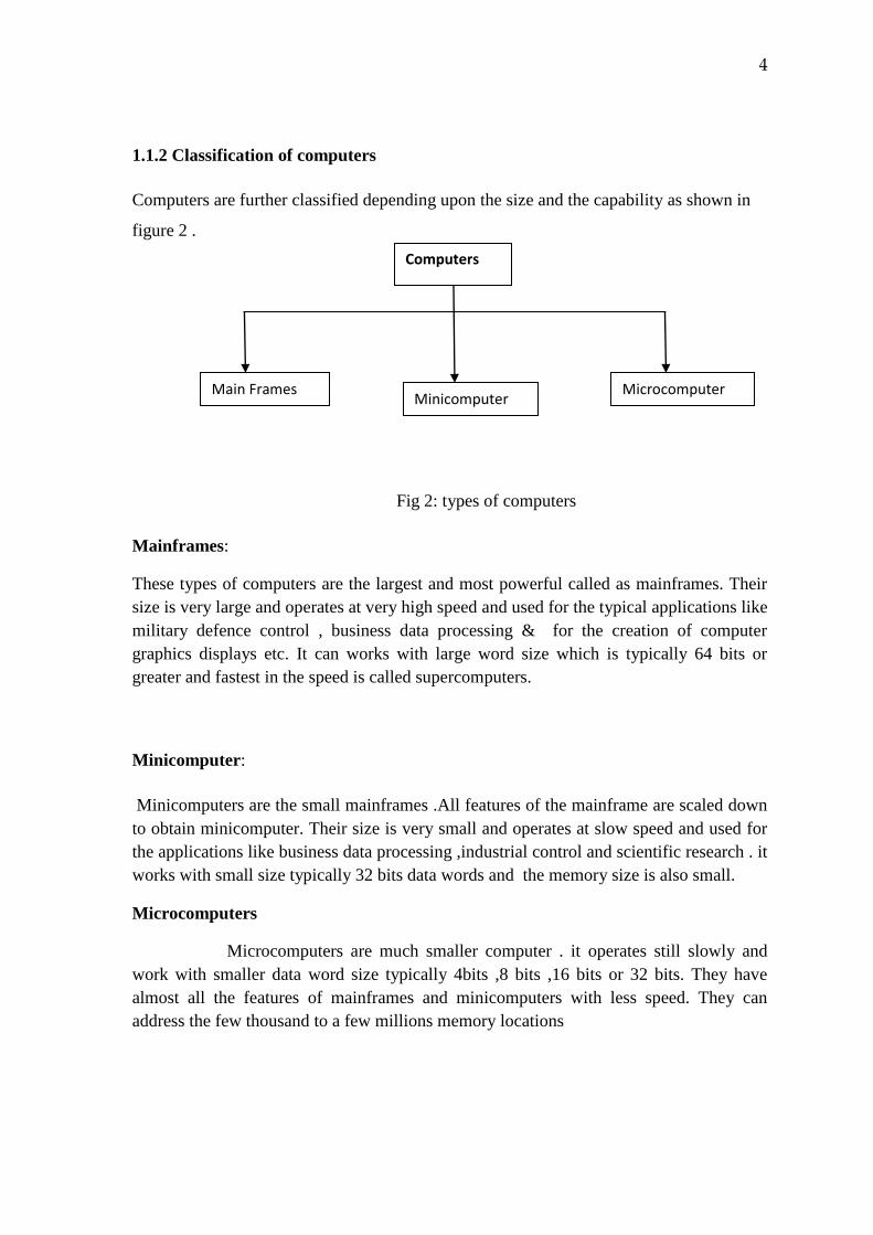
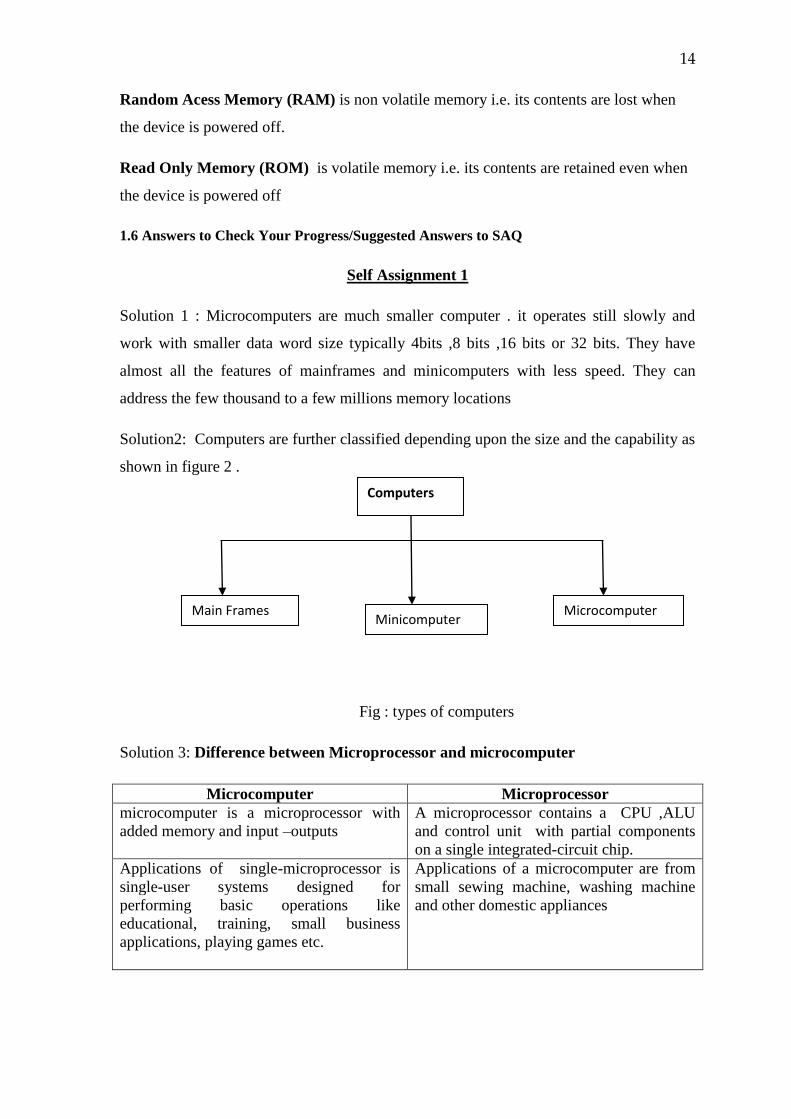
1.1.2 Classification of computers
Computers are further classified depending upon the size and the capability as shown in
figure 2 .
Fig 2: types of computers
Mainframes:
These types of computers are the largest and most powerful called as mainframes. Their
size is very large and operates at very high speed and used for the typical applications like
military defence control , business data processing & for the creation of computer
graphics displays etc. It can works with large word size which is typically 64 bits or
greater and fastest in the speed is called supercomputers.
Minicomputer:
Minicomputers are the small mainframes .All features of the mainframe are scaled down
to obtain minicomputer. Their size is very small and operates at slow speed and used for
the applications like business data processing ,industrial control and scientific research . it
works with small size typically 32 bits data words and the memory size is also small.
Microcomputers
Microcomputers are much smaller computer . it operates still slowly and
work with smaller data word size typically 4bits ,8 bits ,16 bits or 32 bits. They have
almost all the features of mainframes and minicomputers with less speed. They can
address the few thousand to a few millions memory locations
Main Frames Minicomputer
Microcomputer
Computers
5
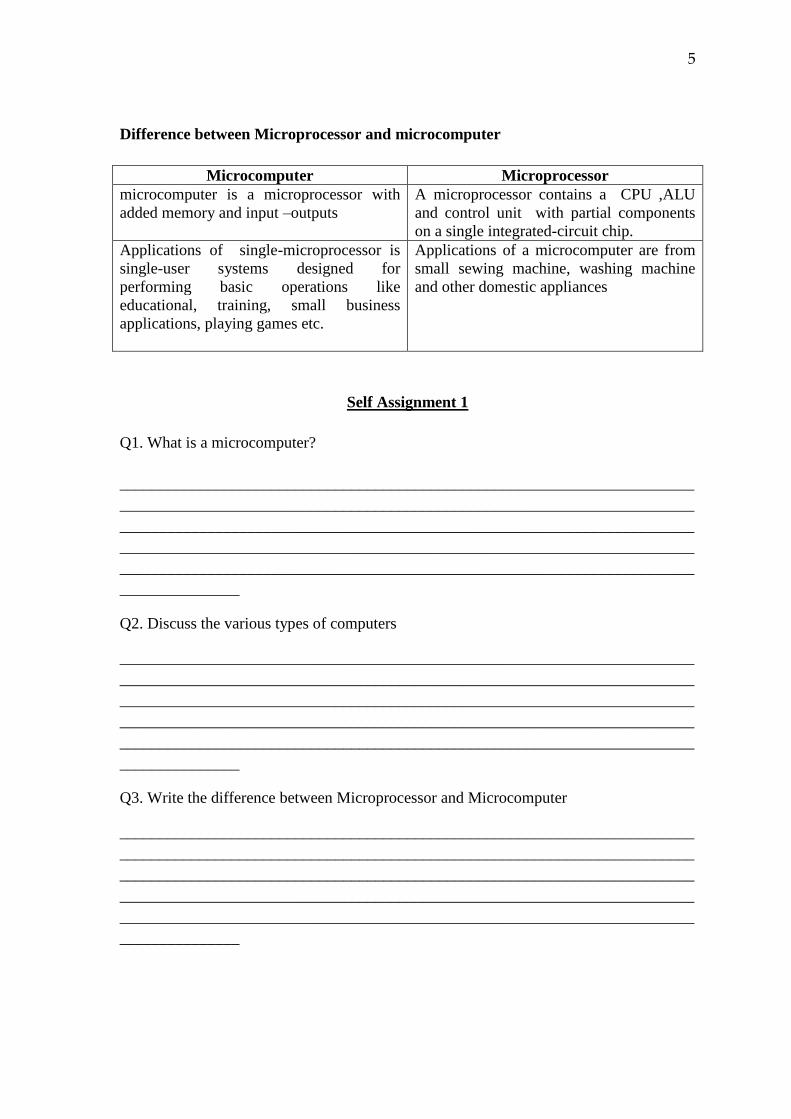
Difference between Microprocessor and microcomputer
Microcomputer Microprocessor
microcomputer is a microprocessor with
added memory and input –outputs
A microprocessor contains a CPU ,ALU
and control unit with partial components
on a single integrated-circuit chip.
Applications of single-microprocessor is
single-user systems designed for
performing basic operations like
educational, training, small business
applications, playing games etc.
Applications of a microcomputer are from
small sewing machine, washing machine
and other domestic appliances
Self Assignment 1
Q1. What is a microcomputer?
________________________________________________________________________
________________________________________________________________________
________________________________________________________________________
________________________________________________________________________
________________________________________________________________________
_______________
Q2. Discuss the various types of computers
________________________________________________________________________
________________________________________________________________________
________________________________________________________________________
________________________________________________________________________
________________________________________________________________________
_______________
Q3. Write the difference between Microprocessor and Microcomputer
________________________________________________________________________
________________________________________________________________________
________________________________________________________________________
________________________________________________________________________
________________________________________________________________________
_______________
6
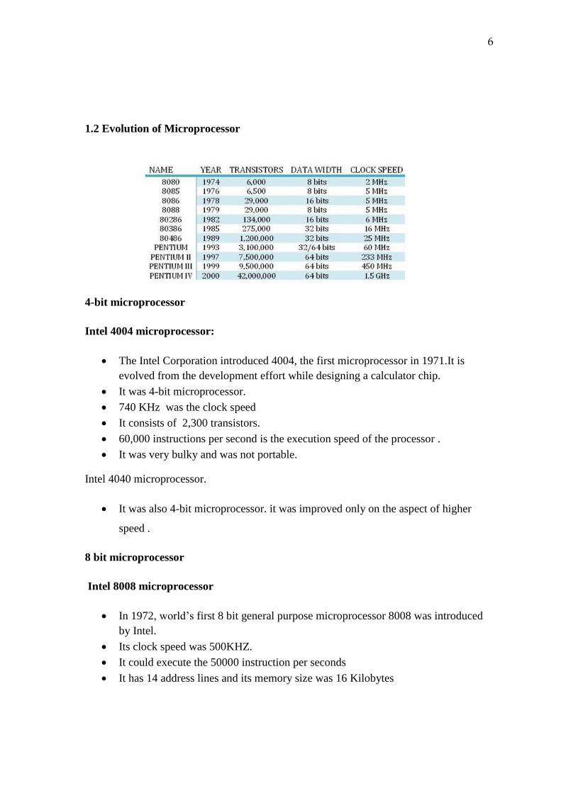
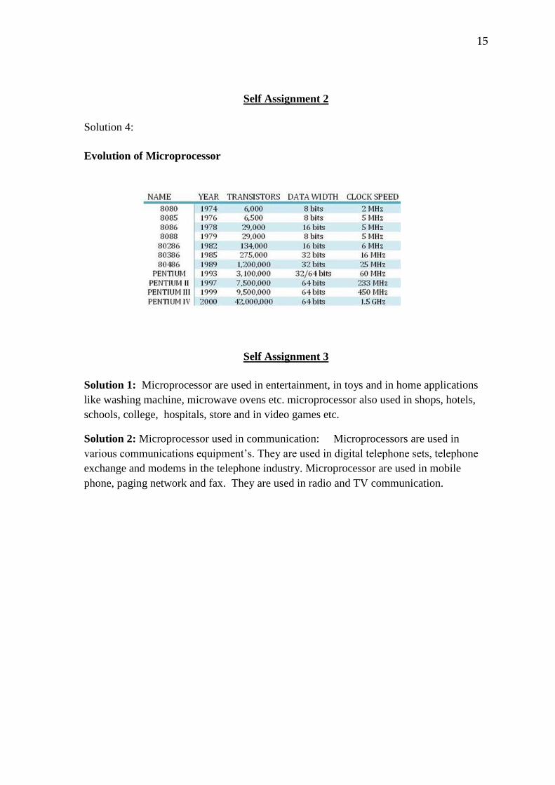
1.2 Evolution of Microprocessor
4-bit microprocessor
Intel 4004 microprocessor:
The Intel Corporation introduced 4004, the first microprocessor in 1971.It is
evolved from the development effort while designing a calculator chip.
It was 4-bit microprocessor.
740 KHz was the clock speed
It consists of 2,300 transistors.
60,000 instructions per second is the execution speed of the processor .
It was very bulky and was not portable.
Intel 4040 microprocessor.
It was also 4-bit microprocessor. it was improved only on the aspect of higher
speed .
8 bit microprocessor
Intel 8008 microprocessor
In 1972, world’s first 8 bit general purpose microprocessor 8008 was introduced
by Intel.
Its clock speed was 500KHZ.
It could execute the 50000 instruction per seconds
It has 14 address lines and its memory size was 16 Kilobytes
7
Intel 8080 microprocessor
The 8080 microprocessor which was the improved version of 8008 was launched
in 1974 by Intel
This 8080 is the much more highly integrated chip than its predecessors which is
built around N-channel MOS technology.
It could address up to 64K.bytes of memory and It could execution speed up to
290,000 operations per second .
It was 10 times faster than 8008.
It was compatible with TTL where as the 8008 was not directly compatible.
Intel 8085 Microprocessor
8 bit microprocessor 8085 was introduced the in the year 1976 by Intel.
The 8085 microprocessor consisted of 6500 MOS transistors and could work at
clock frequencies of 3-5 MHz.
A single +5 volts supply was used for the operation
It has 8 bit data bus and address bus is 16 bit
It had 6500 transistors
It can execute 769230 operations per seconds
It could access the 64 KB of memory
It has 246 instructions.
The main advantage of the same was its internal clock generation controller and
high frequency.
The higher level of the component integration reduced the cost of 8085 and
increased its applications
Intel 8086 Microprocessor
first 16 bit microprocessor was introduced the microprocessor 8085 in the year
1978
the variety of Microprocessors are available depending on the version in which
the clock speed is 4.77 MHZ, 8 MHZ and 10 MHZ
Its data bus is 16 bit and address bus is 20 bits
29000 transistors are used for the same on a single Chip
Execution speed is 2.9 million instructions per seconds.
On chip Memory access up to 1 MB of memory.
It had multiplication and divide instructions.
8
Intel 8088L Microprocessor
In 1979. Intel 8088L Microprocessor which is also 16 bit microprocessor was
introduced as a cheaper version of Intel’s 8086.
It has 8 bit external bus for the 16 bit Microprocessor .
2.5 million instructions per seconds was execution time.
This chip becomes the most popular in the computer industry when IBM used in
Personal computer (PC).
Intel 80186 and 80188 Microprocessor
This microprocessor was introduced in 1982.
It was also16 bit microprocessor
Its clock speed was 6 MHZ
80188 microprocessor was created as a cheaper version of Intel’s 80186.
It was a 16 bit processor with 8 bit external bus.
They had additional components like interrupt controller ,clock generator , local
bus
Intel 80286
In 1982, Intel released 80286 microprocessor which was 16 bits microprocessor.
Microprocessor clock speed was 8MHz.
Data bus was of 16 bit and address bus was of 24 bits.
It was able to address 16 MB of memory.
It consisted 1,34,000 transistor.
It was able to execute 4 million instructions per seconds.
32 bits microprocessors
Microprocessor 80386
In 1986, Intel launched first 32 bit processor that was 80386 microprocessor.
It consisted 275,000 transistor.
It contained 32 bit data bus and 32 bit address bus which made microprocessor to
address up to a total of 4GB memory.
It also contained 64TB virtual memory space.
It was able to process five million instructions per seconds and compatible with all
popular operating systems like windows.
It has 16-bytes of a pre-fetch queue with high memory management capability.
It is included the concept of paging as well as segmentation technique.
80387 math co-processor is used by 80386 microprocessor.
9
80486 microprocessor
Intel released 80486 microprocessor which had 1.2 million transistors.
Other additional features of 80486 microprocessor are built-in math co-processor
and built-in cache.
It was a 32-bit processor but double time faster than 80386.
Bidirectional address bus is used because of cache memory.
It could run at 50MHz clock speed.
Intel Pentium microprocessor:
In 1993, Intel introduce 32-bit Intel Pentium microprocessor.
Original name was 80586 microprocessor then changed to Intel Pentium due to
copyright issues.
It can run at clock speed of 66MHz.
It is able to address 4GB of memory.
Both address and data bus are 32-bit.
110 million instructions per second can be executed by this microprocessor.
Pentium is dual integrated processor which is the important feature. It executes
two non dependent instructions simultaneously.
Intel Pentium pro microprocessor:
In 1995, Intel released the Pentium pro microprocessor .
It was also 32- bit microprocessor.
It has L2 cache of 256 KB.
It had 21 million transistors.
Mainly Pentium processor was launched for the server market.
Pentium pro processor can address either a 4GB memory system or a 64 GB
memory system .
This processor has a 32 bit address either bus if configured for a 64 GB memory
system .
Intel Pentium microprocessor:
In 1997 , Intel released Pentium processor ,instead of being an integrated circuit
as with previous version of microprocessor .
It was also 32 bit microprocessor .
Its clock speed was 233 MHz to 500 MHz.
It could execute 333million instruction per second.
the Xeon is available with L1 ACHE SIZE OF 32KB and a L2 cache with size of
either 512 KB ,1MB or 2MB which is the main difference between the Pentium
and Pentium Xeon .
10
Intel Pentium Microprocessor:
In 1999 Intel released Pentium, which uses a faster core then the
Pentium but it was still a pro Pentium processor.
It was also 32 bit microprocessor.
Its clock speed is varied from 500MHz to 1.4 GHz.
It has 9.5 million transistors.
Intel Pentium Microprocessor:
In late 2000, Intel Pentium 4 microprocessor, initially use P6 architecture, but main
difference is that the Pentium is available in a 1.3 ,1.4,and 1.5 GHz speed version.
Pentium 4 uses the RAMBUS memory technology instead of SDRAM
technology.
It had 42 million of transistors.
All internal connection of this processor was made from aluminium to copper.
Intel Dual core processor:
This processor was introduced in 2006.
This processor was 32-bit or 64- bit.
It had two cores so it called dual processor.
Both core had their own internal bus and L1 cache and share external bus and L2
.
It supported SMT (simultaneously Multi-Treading) technology.
Self Assignment 2
1. In which form CPU provide output:
a. Computer signals
b. Digital signals
c. Metal signals
d. None of these
soln B
2. The main memory in a Personal Computer (PC) is made of
a. cache memory.
b. static RAM
c. Dynamic Ram
d. both (A) and (B).
Soln D
3. Who is the brain of computer:
a. ALU
b. CPU
11
c. MU
d. None of these
Soln B
4. Discuss the Evolution of Microprocessor
__________________________________________________________________
__________________________________________________________________
__________________________________________________________________
_________
1.3 Applications of Microprocessor:
Microprocessor has many application in medical, industrial, defense and consumer
products due to its low cost, low power and small weight/ volume computing capability.
Presently microprocessor based system are used in communication , automation testing of
products ,instrumentation ,speed control of motors ,light intensity control ,automatic
control of generators voltage, temperature control of furnaces, traffic light control etc.
Day by day applications of microprocessor are increasing. There are other various
application of microprocessor ,these are used in Banks, Airline and Railway reservations
,in business organization, Data analysis ,word processing, computer graphics , CAD
machines , industry ,instrumentation, military equipment’s like tanks and radar, office
automation communication s, transportations, consumer goods , automatic testing of
products and control etc.
Another applications of Microprocessor are described below:
1. Microprocessor used in computer graphics: Computers can be used to perform different
function like picture, graphs, charts , drawing. Graphics software package are available
for this purpose . Three dimensional picture and drawing can be prepared with the help of
computers. Building views or machines from different angle can be see with the help of
computer graphics.
2. Microprocessor used in communication:
Microprocessors are used in various communications equipment’s. They are used in
digital telephone sets, telephone exchange and modems in the telephone industry.
Microprocessor are used in mobile phone , paging network and fax. They are used in
radio and TV communication.
3. Microprocessor used in instrumentations :
12
Microprocessor are used in instruments like regulated power supply, frequency
counters , digital millimeter.
Digital storage oscilloscope (DSO) ,function generators , spectrum analyses ,
frequency synthesizers , medical instrument like ECG machines , blood pressure
and temperature monitoring instruments and weighing machines etc.
4. Microprocessor used in traffic light control:
We can see that in now a day there is very heavy road traffic and it can be
controlled easily by the use of microprocessor traffic light.
5. Microprocessor used in word processing and office automation: Word processing
is basically processing storage and retrieval of text data in office with the help of
computer when it is required. Word processing package task are performed by a
software which is known as word processing package. With the help of this
software , the user can create, view , edit, store and print text data.
6. Microprocessor used in Airlines and Railways: Railway and airline reservation
system are implemented with LAN(local area network) and WAN (wide area
network) Microcomputer are used for the reservation in airline and railway .these
microcomputer are placed in different cities and are interconnected to the super
computer with the help of satellite. The user can get information regarding
reservation and can reserve their sheets and also they can get their ticket at their
place. Microcomputer is also used for railway signaling and other controls and for
providing information of trains timing.
7. Microprocessor use in process control: Microprocessor are used as controller to
control various process parameters like speed c, temperature and pressure.
Transducers provide data to the controller then this controller process this data
and generate necessary control signal according to the data.
8. Microprocessor used in consumers: Microprocessor are used in entertainment, in
toys and in home applications like washing machine, microwave ovens etc.
icroprocessor also used in shops, hotels, schools, college, hospitals, store and in
video games etc.
Self Assignment 3
Q1 How microprocessor is helpful in our daily life.
________________________________________________________________________
________________________________________________________________________
________________________________________________________________________
Q2 Discuss the applications of Microprocessor in communication.
________________________________________________________________________
________________________________________________________________________
________________________________________________________________________
13
________________________________________________________________________
____________
1.4 Summary:
A Microprocessor is a semiconductor device that can includes the arithmetic
Logic Unit(ALU) ,registers and a control unit on a single chip. It also called as
Brain of the processing unit that process the digital data.
Buses are bundles of wires that are categorized for unique purpose are called
buses. There type of buses are, data bus pass the data, and address buses pass the
address, and other act as a control lines or bus.
The memory section of microcomputer consists of RAM (random access memory)
as well as ROM (read only memory).
The input/ output section consist of an input device and output device and input
/output ports.
The actual physical devices which are used for interfacing the computer buses
with the external systems are called as ports.
In 1972, world’s first 8 bit general purpose microprocessor 8008 was introduced
by Intel.
8 bit microprocessor 8085 was introduced the in the year 1976 by Intel.
In 1982, Intel released 80286 microprocessor which was 16 bits microprocessor.
Intel released 80486 microprocessor which had 1.2 million transistors.
Intel Dual core processor was introduced in 2006
Microprocessor has many application in medical, industrial, defense and
consumer products due to its low cost, low power and small weight/ volume
computing capability.
1.5 Glossary:
Microcomputer: microcomputer is a microprocessor with added memory and input –
outputs
Microprocessor A microprocessor contains a CPU, ALU and control unit with partial
components on a single integrated-circuit chip.
Central Processing Unit( CPU): The CPU is the heart of the computer which controls
the every device. It is the hardware in a computer that takes the instructions of a from the
program by performing the basic arithmetical, logical, and input/output operations of the
system.
Arithmetic logic unit (ALU): Arithmetic logic unit (ALU) is a digital circuit used to
perform arithmetic and logic operations
14
Random Acess Memory (RAM) is non volatile memory i.e. its contents are lost when
the device is powered off.
Read Only Memory (ROM) is volatile memory i.e. its contents are retained even when
the device is powered off
1.6 Answers to Check Your Progress/Suggested Answers to SAQ
Self Assignment 1
Solution 1 : Microcomputers are much smaller computer . it operates still slowly and
work with smaller data word size typically 4bits ,8 bits ,16 bits or 32 bits. They have
almost all the features of mainframes and minicomputers with less speed. They can
address the few thousand to a few millions memory locations
Solution2: Computers are further classified depending upon the size and the capability as
shown in figure 2 .
Fig : types of computers
Solution 3: Difference between Microprocessor and microcomputer
Microcomputer Microprocessor
microcomputer is a microprocessor with
added memory and input –outputs
A microprocessor contains a CPU ,ALU
and control unit with partial components
on a single integrated-circuit chip.
Applications of single-microprocessor is
single-user systems designed for
performing basic operations like
educational, training, small business
applications, playing games etc.
Applications of a microcomputer are from
small sewing machine, washing machine
and other domestic appliances
Main Frames Minicomputer
Microcomputer
Computers
15
Self Assignment 2
Solution 4:
Evolution of Microprocessor
Self Assignment 3
Solution 1: Microprocessor are used in entertainment, in toys and in home applications
like washing machine, microwave ovens etc. microprocessor also used in shops, hotels,
schools, college, hospitals, store and in video games etc.
Solution 2: Microprocessor used in communication: Microprocessors are used in
various communications equipment’s. They are used in digital telephone sets, telephone
exchange and modems in the telephone industry. Microprocessor are used in mobile
phone, paging network and fax. They are used in radio and TV communication.
16
Chapter 2
Introduction to 8085 Architecture
Structure
2.0 Objectives
2.1 Feature of intel 8085 microprocessors:
2.2 Pin description of 8085
2.2.1 Address Bus and Data Bus
2.2.2 Status and Control Signal
2.2.3 Interrupt Signals
2.2.4 DMA Request Signal
2.3.5 Reset Signals
2.2.6 Serial I/O Signals
2.2.7 Clock Signals
2.2.8 Supply Signals
2.3 Architecture of 8085 microprocessor
2.3.1Register Section
2.3.2Arithmetic and Logical Unit
2.3.3 Instruction Decoder and Machine Cycle Encoder
2.3.4 Address buffer:
2.3.5 Address /data Buffer:
2.3.6 Incrementer / decrementer Address Latch
2.3.7 Interrupt Control
2.3.8 Serial I/O Control Group
2.3.9 Timing and Control
2.0 Objectives
After studying this chapter you will understand
Basics of Architecture of 8085
Functions of the various blocks of 8085
Students will understand the functionality of each pin of 8085
Also understand the concept of flags
17
2.1 FEATURE OF INTEL 8085 MICROPROCESSORS:
1. Intel 8085 microprocessor is an 8-bit microprocessor .it can accept or provide
8-bit data simultaneously.
2. It is a single LSI chip fabricated with 40-pin IC package.
3. It is NMOS device, implemented with 6200 transistors.
4. It requires +5V dc power supply for its operation.
5. Its clock speed is about 3MHz and the clock cycle is of 320 ns , and it provide
on chip clock generator .It does not required external clock generator. but
required external tuned circuits.
6. It consists three main sections
Arithmetic and logic unit (ALU) section
Timing unit section
A set of resisters section
7. It has 74 basic instruction and 256 opcodes.
8. It has 16-bit address lines and 8-bit data line.
9. Lower 8-bit address bus [A0-A7] is multiplexed with higher 8 bit the data bus
[D0-D7], hence ALE Signal is required to separate data lines from address
lines.
10. It provide 16 address lines, hence it can access 2 = 64 K bytes of memory,
program as well as data memory.
11. The 8085 microprocessor 8-bit I/O address, mens it can access 2 =256I/O
ports.
12. It provide 5 hardware interrupts TRAP, RST7.5,RST6.5,RST5.5, and INTR,
these are of two types mask able and non mask able .
13. It provide control signal (IO/M, RD, WR) to control the bus cycles.
14. It provide an 8-bit accumulator ,flags register 6 general purpose resisters
(B,C,D,E,H,L) two special purpose sixteen bit register (SP&PC).
18
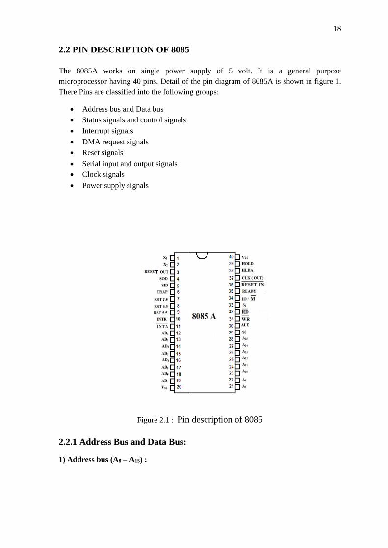
2.2 PIN DESCRIPTION OF 8085
The 8085A works on single power supply of 5 volt. It is a general purpose
microprocessor having 40 pins. Detail of the pin diagram of 8085A is shown in figure 1.
There Pins are classified into the following groups:
Address bus and Data bus
Status signals and control signals
Interrupt signals
DMA request signals
Reset signals
Serial input and output signals
Clock signals
Power supply signals
Figure 2.1 : Pin description of 8085
2.2.1 Address Bus and Data Bus:
1) Address bus (A8 – A15) :
19
These are the output and tristate signals used as higher order 8 bits of 16 bit
address. These signals are unidirectional meaning that the address is given by
8085 to select a memory or an I/O device.
2) Multiplexed address/data bus (AD0 –AD7):
These are input/output, tristate signals having two set of signals. This bus contains
address of all data signal. The data bus is used to multiplex or time shared lower
order 8 bits, of 16 bit address.
2.2.2 Status and Control Signals:
1) Address latch enable (ALE):
This is output signal, used to give the information of AD0 – AD7 contents which is
given by ALE.
During the first clock of a machine cycle a positive pulse is generated.
When the pulse generated by the machine cycle is high it show the contents of
AD0 - AD7 are address and if the machine cycle is low it indicates the contents are
data.
AD0 – AD7 (i.e. demultiplex)is seperated into A0 – A7 and D0 – D7 using ALE
signal . This separation is done with the help of latch connected to AD0 – AD7
lines and this latch is controlled by ALE signal.
2) Input Output/ Memory (IO/��):
This is an output status signal which is used to give information of operation
which is performed with memory or I/O device .If IO/�� = 0 then microprocessor
is performing a memory related operation.
If IO/�� =1 then microprocessor is performing an I/O device related operation.
3) Status signals(S1 and S0):
These output status signals are used to give information of operation to be
done by microprocessor. The four different conditions of 8085 machine
cycles are specified by S0 and S1 lines.
These four cycles are as follows:
S.NO OPERATION S0 S1
(1) Halt 0 0
(2) Read (Data read from memory) 0 1
(3) Write 1 0
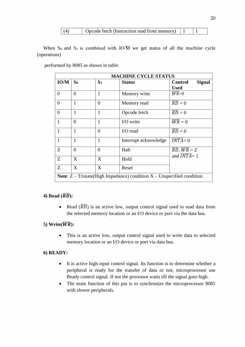
20
(4) Opcode fetch (Instruction read from memory) 1 1
When S0 and S1 is combined with IO/M we get status of all the machine cycle
(operations)
performed by 8085 as shown in table:
MACHINE CYCLE STATUS
IO/M S0 S1 Status Control Signal
Used
0 0 1 Memory write 𝑊𝑅 =0
0 1 0 Memory read 𝑅𝐷 = 0
0 1 1 Opcode fetch 𝑅𝐷 = 0
1 0 1 I/O write 𝑊𝑅 = 0
1 1 0 I/O read 𝑅𝐷 = 0
1 1 1 Interrupt acknowledge 𝐼𝑁𝑇𝐴 = 0
Z 0 0 Halt 𝑅𝐷 , 𝑊𝑅 = Z
and 𝐼𝑁𝑇𝐴 = 1
Z X X Hold
Z X X Reset
Note: Z – Tristate(High Impedance) condition X – Unspecified condition
4) Read (𝑹𝑫):
Read (𝑅𝐷 ) is an active low, output control signal used to read data from
the selected memory location or an I/O device or port via the data bus.
5) Write(𝑾𝑹 ):
This is an active low, output control signal used to write data to selected
memory location or an I/O device or port via data bus.
6) READY:
It is active high input control signal. Its function is to determine whether a
peripheral is ready for the transfer of data or not, microprocessor use
Ready control signal. If not the processor waits till the signal goes high.
The main function of this pin is to synchronize the microprocessor 8085
with slower peripherals.
21
2.2.3 Interrupt Signals :
(1) TRAP:
It is an actively high, edge triggered,level triggered and non-maskable, highest
priority interrupt.
When TRAP line is active microprocessor performs internal restart automatically
at address 002H.
(2) Restart interrupts (RST 7.5, RST 6.5 and RST 5.5):
These are active high, triggered mask able interrupt. They cause an internal restart
to be automatically inserted.
The priorities of these are RST 7.5, RST 6.5, RST 5.5.
When RST 7.5, RST 6.5 or RST 5.5 is active microprocessor performs internal
restart automatically at addresses 003H.003H, 002CH respectively.
(3) INTR
INTR is an level triggered and active high general purpose interrupt.
It has the lowest priority.
(4) 𝑰𝑵𝑻𝑨
𝐼𝑁𝑇𝐴 is used to indicate that the microprocessor has received an INTR interrupt.
2.2.4 DMA Request Signal:
HOLD and HLDA:
HOLD is an active high, input signal used by other controller to request
microprocessor about use of address, data and control signals.
The microprocessor in response to HOLD generates a signal to acknowledge the
requesting device by HLDA signal. When HLDA is active it indicates that
microprocessor has received HOLD request and will relinquish the buses in next
clock cycle. The other controller will use buses and upon completion of work will
remove HOLD signal, because of this microprocessor will also make HLDA low.
This microprocessor takes control of buses half clock cycle after HLDA goes low.
2.3.5 Reset Signals:
𝑹𝑬𝑺𝑬𝑻 𝑰𝑵 :
This is an active low ,input reset signal. When 𝑅𝐸𝑆𝐸𝑇 𝐼𝑁 =0, it clears program
counter i.e. 0000and makes address, data and control lines tristated. After reset the
status of internal register and lags are predictable.
The CPU is held in the reset condition as long as 𝑅𝐸𝑆𝐸𝑇 𝐼𝑁 is applied .
After reset the microprocessor starts executing instructions from 0000H onwards.
22
RESET OUT:
It is an active high output signal used to indicate that the microprocessor is reset
.This signal is used as system reset, to reset other devices connected in system.
2.2.6 Serial I/O Signals:
(1) SID (Serial output data):
This is an active high, serial output port pin, used to transfer serial 1 bit data under
software control.
When a RIM instruction is executed the SID pin data is loaded in bit D7 of
accumulator.
(2) SOD (Serial output data):
This is an active high, serial output port pin, used to transfer serial 1 bit data under
software control.
When a SIM instruction is executed the SOD pin is set or reset depending on D7
and D6 bits of accumulator.
2.2.7 Clock Signals:
(1) X1X2:
These are clock input signals, connected to crystal, LC or RC network. The X1
and X2 pins drive the internal clock generator circuit.
The frequency is divided by 2 and used as operating frequency. Generally the
6.014 MHz crystal is connected to X1 and X2, this is divided by 2. Do, the
operating frequency of 8085 is 3.07 MHz.
(2) CLK OUT:
This is an output signal, used as a system clock. The internal operating frequency
is available on CLK OUT pin.
2.2.8 Supply Signals:
Vcc and Vss:
Power supply VCC - +5 V, Vss- Ground reference.
Self Assessment 1
Q1 List the main features of 8085 microprocessor
23
________________________________________________________________________
________________________________________________________________________
________________________________________________________________________
_______________
Q2: What are the Serial I/O Signals.
________________________________________________________________________
________________________________________________________________________
________________________________________________________________________
_______________
Q3 Discuss the significance of Address latch enable (ALE) pin in 8085
microprocessor.
________________________________________________________________________
________________________________________________________________________
________________________________________________________________________
__________________
2.3 ARCHITECTURE OF 8085 MICROPROCESSOR
This architecture is divided in different groups as follows:
Registers
Arithmetic and logic unit
Instruction decoder and machine cycle encoder
Address/Data Buffer
Incrementer / Decrementer Address Latch
Interrupt control
Serial I/O control
Timing and control circuitry
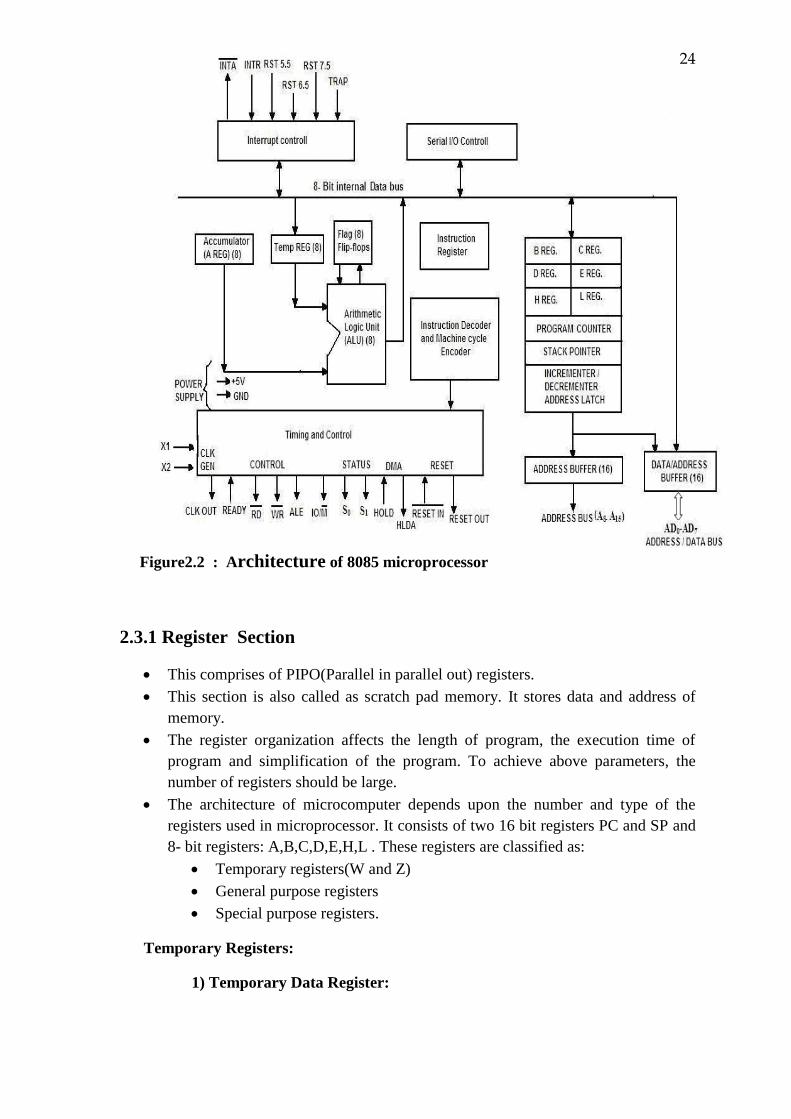
24
Figure2.2 : Architecture of 8085 microprocessor
2.3.1 Register Section
This comprises of PIPO(Parallel in parallel out) registers.
This section is also called as scratch pad memory. It stores data and address of
memory.
The register organization affects the length of program, the execution time of
program and simplification of the program. To achieve above parameters, the
number of registers should be large.
The architecture of microcomputer depends upon the number and type of the
registers used in microprocessor. It consists of two 16 bit registers PC and SP and
8- bit registers: A,B,C,D,E,H,L . These registers are classified as:
Temporary registers(W and Z)
General purpose registers
Special purpose registers.
Temporary Registers:
1) Temporary Data Register:
25
It is called as 8 bit operand register . It provides operands to ALU.
The ALU can store intermediate result in temporary register. It is not
available to user.
Example: ADD B instruction adds A register and B register contents, the
result is stored in A register. In this case one data is available in A register.
the other data is available in B register. The data from B register is
transferred to temporary register. Contents of A register and temporary
register will be added up by ALU and the result is stored in Accumulator.
The temporary register is also used for other operations such as register to
register data transfer, etc.
2) Temporary Registers (W and Z):
The temporary registers serve as one input to the ALU . The other input to
the ALU is from the accumulator.
These registers are not available to the user . They are internally used by
the mic, during arithmetic and logic operation, registers are used to hold
the data by control section.
These registers hold 8 bit data.
General Purpose Registers:
The 8085 microprocessor contains 8 bit general purpose registers named
as B, C, D, E, H and L.
B, C, D, E, H and can be used to store 8 bits of data or can be u send to
form a register pair to store 16 bit data.
BC, DE and HL are available register pairs.
users can programmed these registers. These registers are available to the
user. Results of arithmetic and logical operations, address of data memory
and data to be stored by these registers.
The HL register pair functions as data pointer and memory pointer. If used
as data pointer it holds the address of a 16 bit address of a memory
location.
Use of General Purpose Registers & How do they Increase the speed of
Operation :
The main use to hold data which is frequency used.
It increases the speed of program execution. The main reason is as follows.
The data in microprocessor can be stored in memory or general purpose
registers. If the data is present in memory the microprocessor has to
perform an operation of memory read. The data is taken by
microprocessor, the required operation is performed and result is stored
back to memory. To store result in memory the microprocessor has to
26
perform one or more operation of memory write. Thus there are two
operations involved in using memory to hold data.
But if data is present in general purpose register there is no operation
involved. The microprocessor does not have to perform any external
memory read and write operation. Thus the time required to execute
program using general purpose registers is very less as compared to
program using memory.
Special Purpose Registers:
These are used for special use. The special purpose registers are:
Accumulator
Flag Register
Instruction Register
Program Counter
Stack Pointer
1) Accumulator :
It is a general purpose register of the microprocessor also called as A
register. The name of the register is derived from the arithmetic addition
process.
It is a multipurpose register that can be used for data storage, arithmetic,
logical, input/output operations.
It is used as a general purpose register to store 8 bit of data.
It is also used to store the result of operation performed by arithmetic and
logical unit.
2) Flag register or (Program Status word). It is an 8- bit register which gives the data
conditions in the accumulator with certain exceptions. So this flag register is called as
Status register. It is an eight bit register, it contains only 5 flag bits and the pending three
bits are undefined as shown in Fig:
Figure 2.3 Flag register
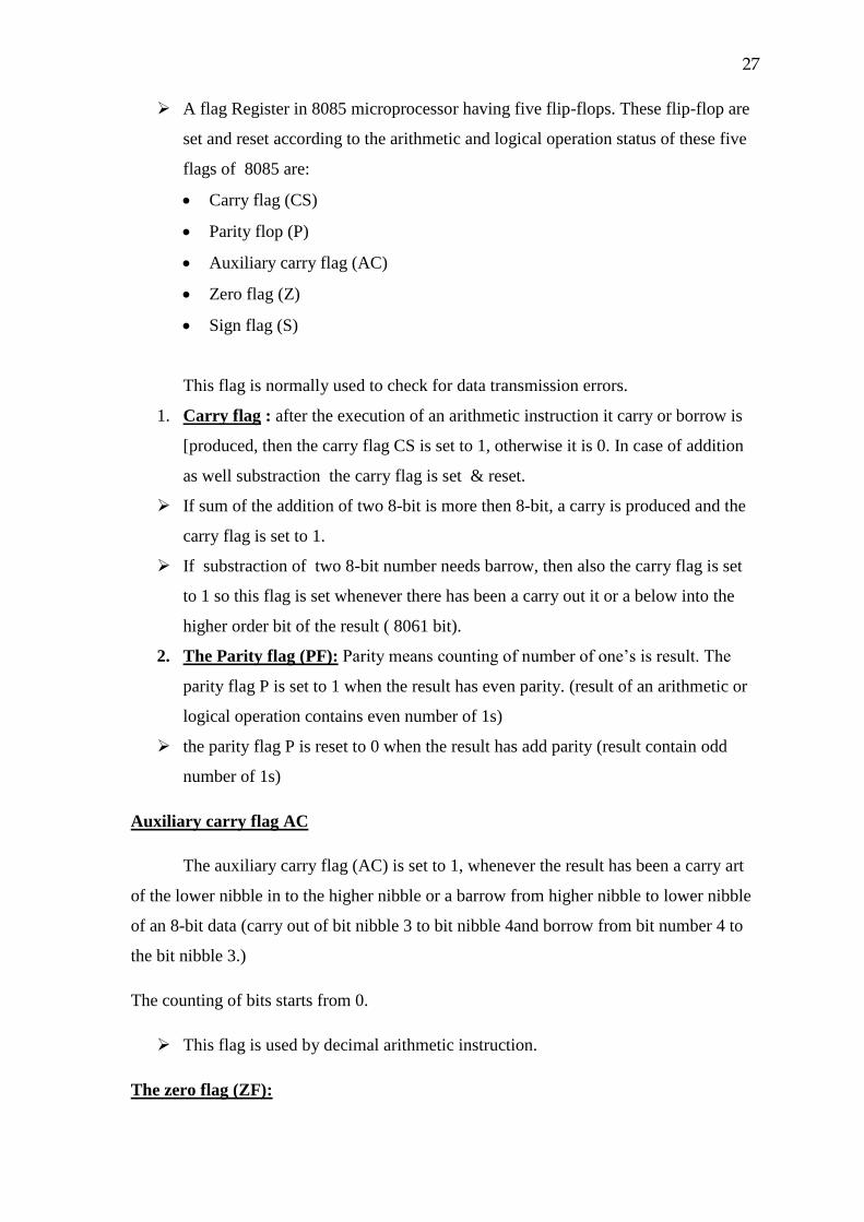
27
A flag Register in 8085 microprocessor having five flip-flops. These flip-flop are
set and reset according to the arithmetic and logical operation status of these five
flags of 8085 are:
Carry flag (CS)
Parity flop (P)
Auxiliary carry flag (AC)
Zero flag (Z)
Sign flag (S)
This flag is normally used to check for data transmission errors.
1. Carry flag : after the execution of an arithmetic instruction it carry or borrow is
[produced, then the carry flag CS is set to 1, otherwise it is 0. In case of addition
as well substraction the carry flag is set & reset.
If sum of the addition of two 8-bit is more then 8-bit, a carry is produced and the
carry flag is set to 1.
If substraction of two 8-bit number needs barrow, then also the carry flag is set
to 1 so this flag is set whenever there has been a carry out it or a below into the
higher order bit of the result ( 8061 bit).
2. The Parity flag (PF): Parity means counting of number of one’s is result. The
parity flag P is set to 1 when the result has even parity. (result of an arithmetic or
logical operation contains even number of 1s)
the parity flag P is reset to 0 when the result has add parity (result contain odd
number of 1s)
Auxiliary carry flag AC
The auxiliary carry flag (AC) is set to 1, whenever the result has been a carry art
of the lower nibble in to the higher nibble or a barrow from higher nibble to lower nibble
of an 8-bit data (carry out of bit nibble 3 to bit nibble 4and borrow from bit number 4 to
the bit nibble 3.)
The counting of bits starts from 0.
This flag is used by decimal arithmetic instruction.
The zero flag (ZF):
28
the zero flag z is set to 1, if the results of an arithmetic or logical operation is 0.
Otherwise zero flag Z is set to 0.( if results is not zero)
The sign flag (S):
The sign flag s is set to 1 if the result of an arithmetic and logical operation is
negative.
Otherwise the sign flag S is set to 0( if the result is positive).
This flag has its significance only when signed arithmetic operation is performed.
The most significant bit (MSB) is used as a sign bit.
Program status word (ASW):
Five bits indicates the five status flags and remaining three bits are undefined.
Combinations of these 8 bits is called program status word.
The accumulator and PSW are treated as a 16-bit unit for stack operation.
3) Instruction Register:
Opcode of the instruction is hold by the instruction register which is being
decoded and executed.
The opcode is further sent to the instruction decoder to pick one of the 256
alternatives.
4) Program Counter (PC):
Address of program memory is hold by program counter.
It indicates toward the next instruction to be fetched i.e. it hold the
memory address of next instruction to be executed.
When reset is activated, the address of the first instruction to be fetched
and executed by the program counter. For 8085 the reset address is 0000H.
During fetch operation, the microprocessor places contents of program
counter (PC) on address bus and fetches very first byte of instruction from
that memory location and then microprocessor increments program to the
point to the next byte of the instruction.
The size of program counter directly depends number of address bits .In
case of 8085 microprocessor it is 16 bit .
In jump and call instructions, program counter is places the address given
for the jump and call instructions. If the condition meets then the processor
fetches next instruction from the new address given by JUMP or CALL
29
instruction otherwise the 8085 continues with the next instruction after
CALL or JUMP instruction.
5) Stack Pointer (SP) :
Stack is a reversed part of memory where register pair information taken
back by software control or to be stored. This area of memory is called as
stack area.
This is a 16 bit register and called as the stack starting address. It is always
points at upper side of the stack.
Data stored on stack is used to be track.
The stack pointer is incremented and decremented after each stack read
and write operation respectively.
Transfer type instruction is used to load an initial value in stack pointer.
Assigned stack in memory has initial value must be at the highest address
of an memory.
Stack should be always initialized in data memory.
2.3.2 Arithmetic and Logical Unit:
This section processes data i.e. it performs arithmetic and logical
operations.
It performs arithmetic like addition, subtraction and logical operation like
ANDing, ORing, EXORing,etc.
The ALU is not available to the user. Its word length depends upon the
width of an internal data bus. Generally it is 8 bit.
The ALU is always used to controlled by timing and control circuits.
It accept operand from temporary register and accumulator . It stores result
of the arithmetic and logic operations in accumulator or temporary
register.
It provides status of the result into the flag register.
Branching decisions is taken by ALU.
2.3.3 Instruction Decoder and Machine Cycle Encoder:
Instruction register gives a bit pattern (opcode) to instruction decoder.
further, which gives decoded information to control logic.
The information contains what type of operations to be performed, who
will going to perform it and how many bytes of instruction contains .
Instruction in this block will be understand by the decoder.
The 8085 executes such seven types of machine cycles. The machine cycle
encoder gives information about which cycle is currently executed.
2.3.4 Address buffer:
Buffer used for to address lines. This is an 8 bit unidirectional buffer.
30
It is used to drive the higher order address bus.
When they are not in use or under certain conditions such as reset ,hold
,halt ,this buffer is used to tri-state to address lines.
2.3.5 Address /data Buffer:
bidirectional buffer is used for both address and data.
It is used to drive the lower order address and data bus.
This buffer is used tri- state to address/data lines for reset , hold , halt
conditions
2.3.6 Incremented / decremented Address Latch:
This 16 bit register is used to increment or decrement the contents of PC
and SD registers.
2.3.7 Interrupt Control:
This block accepts different interrupt request inputs such as,TRAP,RST7.5,
RST6.5, RST5.5 and INTR .When a valid interrupt request is present it
informs control logic to take action in response to each signal.
2.3.8 Serial I/O Control Group:
The data transferred in to the lines is going to be parallel data , but under
some conditions it is useful to use serial data transfer. 8085 apply by using
SID and SOD signals. The data on these lines is accepted or transferred
under software control by serial I/O control block . In 8085 to perform
serial data transfer there are two special instructions RIM and SIM.
2.3.9 Timing and Control:
This is a control section of 8085 made up of synchronous sequential logic
circuit.
It controls all internal and external circuits.
It operates with reference to clock signal.
It takes information from decoder and generates micro steps to perform.
Moreover, the block accepts clock inputs, synchronising operations and
perform sequencing. The synchronization is mandatory for communication
between microprocessor and other peripheral devices. It uses different
status and control signals for implementation.
31
Self Assessment 2
Q1 Draw a neat block diagram of Architecture of 8085 Microprocessor. Explain the
function of each block.
________________________________________________________________________
________________________________________________________________________
________________________________________________________________________
_______________
Q2 What are the different type of flags available in 8085 microprocessor
________________________________________________________________________
________________________________________________________________________
________________________________________________________________________
______________
Q3 Discuss the functions of Timing and Control unit.
________________________________________________________________________
________________________________________________________________________
________________________________________________________________________
_______________
Q4 Fill in the Blanks
1) ____ causes the address of the next microprocessor to be obtained from the memory:
a. CRJA b. ROM c. MAP
d. HLT
2) _________ Stores the instruction currently being executed:
a. Instruction register b. Current register
c. Both a and b d. None of these
3) The status register is also called the____:
a. Condition code register
b. Flag register
c. A and B
d. None of these
32
4) BCD stands for……………………..
a. Binary coded decimal b. Binary coded decoded
c. Both a & b d. none of these
5) Which is used to store critical pieces of data during subroutines and interrupts:
a. Stack
b. Queue
c. Accumulator
d. Data register
6) The area of memory with addresses near zero are called_____________
a. High memory b. Mid memory
c. Memory d. Low memory
7) The processor uses the stack to keep track of where the items are stored on it this by
using the__________________
a. Stack pointer register b. Queue pointer register
c. Both a & b d. None of these
8) Which point to the ___ of the stack:
a. TOP
b. START
c. MID
d. None of these
Summary
Intel 8085 microprocessor is an 8-bit microprocessor .it can accept or
provide 8-bit data simultaneously.
Its clock speed is about 3MHz and the clock cycle is of 320 ns , and it
provide on chip clock generator .It does not required external clock
generator. but required external tuned circuits.
It consists three main sections: Arithmetic and logic unit (ALU)
section, Timing unit section, A set of resisters section
It has 74 basic instruction and 256 opcodes.
It has 16-bit address lines and 8-bit data line.
Lower 8-bit address bus [A0-A7] is multiplexed with higher 8 bit the
data bus [D0-D7], hence ALE Signal is required to separate data
lines from address lines.
It provide 16 address lines, hence it can access 2 = 64 K bytes of
memory, program as well as data memory.
33
It provide an 8-bit accumulator ,flags register 6 general purpose
resisters (B,C,D,E,H,L) two special purpose sixteen bit register
(SP&PC).
Glossary:
Arithmetic logic unit (ALU): Arithmetic logic unit (ALU) is a digital circuit used
to perform arithmetic and logic operations
Address latch enable (ALE):This is output signal, used to give the information of
AD0 – AD7 contents which is given by ALE.
SID (Serial output data):This is an active high, serial output port pin, used to
transfer serial 1 bit data under software control.
SOD (Serial output data):his is an active high, serial output port pin, used to
transfer serial 1 bit data under software control.When a SIM instruction is
executed the SOD pin is set or reset depending on D7 and D6 bits of accumulator.
Accumulator :• It is a general purpose register of the microprocessor also
called as A register. The name of the register is derived from the arithmetic
addition process
flag Register : In 8085 microprocessor having five flip-flops. These flip-flop are
set and reset according to the arithmetic and logical operation status of these five
flags of 8085 are:
Carry flag (CS),Parity flag (P),Auxiliary carry flag (AC),Zero flag (Z),Sign flag
(S)
Program Counter (PC):Address of program memory is hold by program counter.it
indicates toward the next instruction to be fetched i.e. it hold the memory address
of next instruction to be executed.
Stack Pointer (SP) :Stack is a reversed part of memory where register pair
information taken back by software control or to be stored. This area of memory
is called as stack area.
This is a 16 bit register and called as the stack starting address
TRAP: It is an actively high, edge triggered,level triggered and non-maskable,
highest priority interrupt.When TRAP line is active microprocessor performs
internal restart automatically at address 002H
HOLD : HOLD is an active high, input signal used by other controller to request
microprocessor about use of address, data and control signals.
Answers to Check Your Progress/Suggested Answers to SAQ
Self Assessment 1 Q1
a) Intel 8085 microprocessor is an 8-bit microprocessor .it can accept or provide 8-
bit data simultaneously.
34
b) Its clock speed is about 3MHz and the clock cycle is of 320 ns , and it provide on
chip clock generator .It does not required external clock generator. but required
external tuned circuits.
c) It consists three main sections: Arithmetic and logic unit (ALU) section, Timing
unit section, A set of resisters section
d) It has 74 basic instruction and 256 opcodes.
e) It has 16-bit address lines and 8-bit data line.
f) Lower 8-bit address bus [A0-A7] is multiplexed with higher 8 bit the data bus
[D0-D7], hence ALE Signal is required to separate data lines from address lines.
g) It provide 16 address lines, hence it can access 2 = 64 K bytes of memory,
program as well as data memory.
h) It provide an 8-bit accumulator ,flags register 6 general purpose resisters
(B,C,D,E,H,L) two special purpose sixteen bit register (SP&PC).
Q2 Serial I/O Signals:
(a) SID (Serial output data):This is an active high, serial output port pin, used to
transfer serial 1 bit data under software control. When a RIM instruction is
executed the SID pin data is loaded in bit D7 of accumulator.
(b) SOD (Serial output data):This is an active high, serial output port pin, used
to transfer serial 1 bit data under software control. When a SIM instruction is
executed the SOD pin is set or reset depending on D7 and D6 bits of accumulator.
Q3
Address latch enable (ALE): This is output signal, used to give the information
of AD0 – AD7 contents which is given by ALE. During the first clock of a machine cycle
a positive pulse is generated. When the pulse generated by the machine cycle is high it
show the contents of AD0 - AD7 are address and if the machine cycle is low it indicates
the contents are data. AD0 – AD7 (i.e. demultiplex)is separated into A0 – A7 and D0 – D7
using ALE signal . This separation is done with the help of latch connected to AD0 – AD7
lines and this latch is controlled by ALE signal.
Self Assessment2
Q1 This architecture is divided in different groups as follows:
Registers
35
Arithmetic and logic unit
Instruction decoder and machine cycle encoder
Address/Data Buffer
Incrementer / Decrementer Address Latch
Interrupt control
Serial I/O control
See the section 2.3 for detail with figure .
Q2 A flag Register in 8085 microprocessor having five flip-flops. These flip-flop are set
and reset according to the arithmetic and logical operation status of these five flags of
8085 are:
Carry flag (CS)
Parity flop (P)
Auxiliary carry flag (AC)
Zero flag (Z)
Sign flag (S)
Q3 Timing and Control: This is a control section of 8085 made up of synchronous
sequential logic circuit. It controls all internal and external circuits. It operates with
reference to clock signal. It takes information from decoder and generates micro steps to
perform. Moreover, the block accepts clock inputs, synchronising operations and
perform sequencing. The synchronization is mandatory for communication between
microprocessor and other peripheral devices. It uses different status and control signals
for implementation.
36
Chapter 3
Instruction set 8085
3.0 Objectives
3.1 Introduction
3.2 Data Transfer Group
3.3 Arithmetic Instructions
3.4 Logical Instructions
3.5 Branch Group Instructions
3.6 Control Instructions
3.0 Objectives
This chapter provides the details of various instructions used for the 8085. After reading this
chapter you will be able to
What are the various instructions sets used for 8085
How to differentiate between various instructions sets
The basic operations of instructions
Use of instructions to execute the desired task
Efficient use of instructions to execute a program
3.1 Introduction An Instruction is a command for the microprocessor/computer to perform a definite operation
on provided data. Whereas, the instruction set is the collection of the instructions that the
microprocessor is designed to execute. Each and every instruction is denoted by an op-code
which is different for different manufacturer.If Intel Corporation has its own instruction for self-
made processors, they cannot be used by other microprocessor manufactures. These
instructions for 8085 microprocessor are classified into the following groups.
Data Transfer Group
Arithmetic Group
Logical Group
Branch Control Group
I/O and Machine Control Group
3.2 Data Transfer Group
This group contains only those Instructions, which are used to transfer data from one register to
another register, from memory to register or register to memory. Examples are: MOV, MVI, LXI,
LDA, STA etc. While performing the instruction from this group, the contents of the source
remains altered and only the process of copy & place takes place. For example copy
37
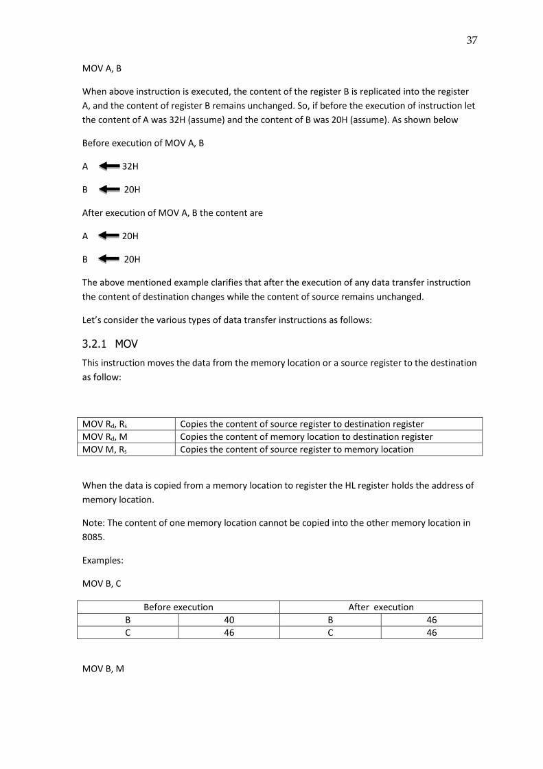
MOV A, B
When above instruction is executed, the content of the register B is replicated into the register
A, and the content of register B remains unchanged. So, if before the execution of instruction let
the content of A was 32H (assume) and the content of B was 20H (assume). As shown below
Before execution of MOV A, B
A 32H
B 20H
After execution of MOV A, B the content are
A 20H
B 20H
The above mentioned example clarifies that after the execution of any data transfer instruction
the content of destination changes while the content of source remains unchanged.
Let’s consider the various types of data transfer instructions as follows:
3.2.1 MOV
This instruction moves the data from the memory location or a source register to the destination
as follow:
MOV Rd, Rs Copies the content of source register to destination register
MOV Rd, M Copies the content of memory location to destination register
MOV M, Rs Copies the content of source register to memory location
When the data is copied from a memory location to register the HL register holds the address of
memory location.
Note: The content of one memory location cannot be copied into the other memory location in
8085.
Examples:
MOV B, C
Before execution After execution
B 40 B 46
C 46 C 46
MOV B, M
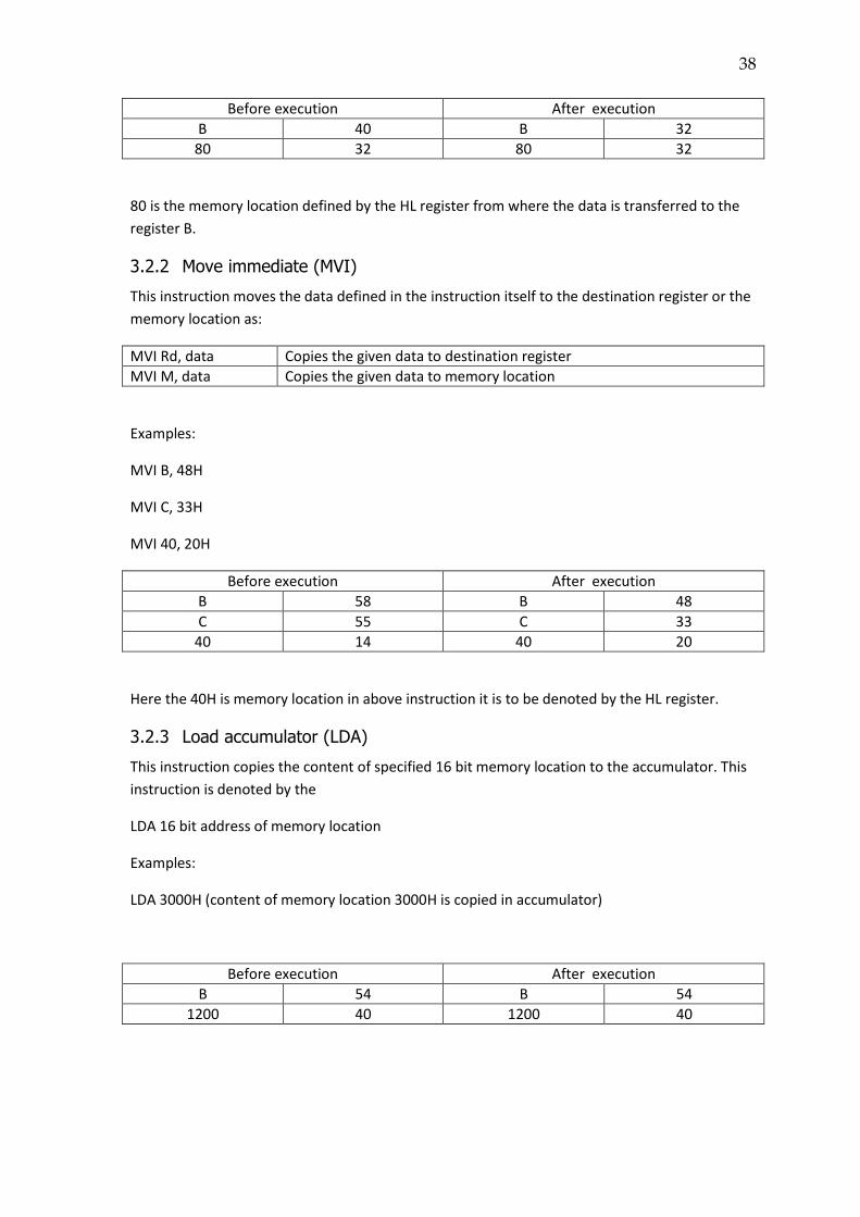
38
Before execution After execution
B 40 B 32
80 32 80 32
80 is the memory location defined by the HL register from where the data is transferred to the
register B.
3.2.2 Move immediate (MVI)
This instruction moves the data defined in the instruction itself to the destination register or the
memory location as:
MVI Rd, data Copies the given data to destination register
MVI M, data Copies the given data to memory location
Examples:
MVI B, 48H
MVI C, 33H
MVI 40, 20H
Before execution After execution
B 58 B 48
C 55 C 33
40 14 40 20
Here the 40H is memory location in above instruction it is to be denoted by the HL register.
3.2.3 Load accumulator (LDA)
This instruction copies the content of specified 16 bit memory location to the accumulator. This
instruction is denoted by the
LDA 16 bit address of memory location
Examples:
LDA 3000H (content of memory location 3000H is copied in accumulator)
Before execution After execution
B 54 B 54
1200 40 1200 40
39
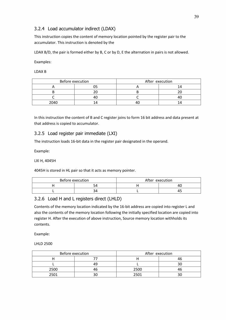
3.2.4 Load accumulator indirect (LDAX)
This instruction copies the content of memory location pointed by the register pair to the
accumulator. This instruction is denoted by the
LDAX B/D, the pair is formed either by B, C or by D, E the alternation in pairs is not allowed.
Examples:
LDAX B
Before execution After execution
A 05 A 14
B 20 B 20
C 40 C 40
2040 14 40 14
In this instruction the content of B and C register joins to form 16 bit address and data present at
that address is copied to accumulator.
3.2.5 Load register pair immediate (LXI)
The instruction loads 16-bit data in the register pair designated in the operand.
Example:
LXI H, 4045H
4045H is stored in HL pair so that it acts as memory pointer.
Before execution After execution
H 54 H 40
L 34 L 45
3.2.6 Load H and L registers direct (LHLD)
Contents of the memory location indicated by the 16-bit address are copied into register L and
also the contents of the memory location following the initially specified location are copied into
register H. After the execution of above instruction, Source memory location withholds its
contents.
Example:
LHLD 2500
Before execution After execution
H 77 H 46
L 49 L 30
2500 46 2500 46
2501 30 2501 30
40
The content of given memory location are copied to H register and the content of next memory
location are copied to L register. The content of memory location remains unaltered.
3.2.7 Store accumulator direct (STA)
By using STA, contents of the accumulator register are copied into the specified memory
location. 16 bit memory location is stated through the operand. Therefore it is a 3-byte
instruction, 2 bytes for the address of the location and 1 byte for the instruction itself. First of
the 2 bytes reserved for location specifies the low-order address and the next byte specifies the
high-order address.
Example:
STA 4630
Before execution After execution
A 20 A 20
4630 34 4630 20
This instruction is applicable to register ‘A’ only. So, we cannot have instruction like STB.
3.2.8 Store accumulator indirect (STAX)
It is a type of indirect addressing since the location in which the contents of accumulator are to
be copied is not specified directly. Rather the location address is specified through the contents
of a register pair. The contents of the accumulator and register pair remain un-altered.
Examples:
STAX B
Before execution After execution
A 77 A 77
B 33 B 33
C 00 C 00
3300 13 3300 77
The content of accumulator are copied into the memory location pointed by the register pair,
the content of register pair and the accumulator remains unchanged.
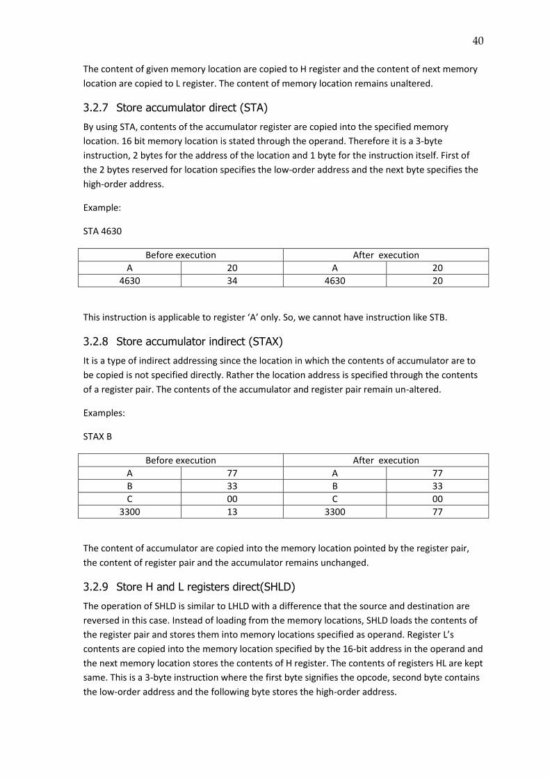
3.2.9 Store H and L registers direct(SHLD)
The operation of SHLD is similar to LHLD with a difference that the source and destination are
reversed in this case. Instead of loading from the memory locations, SHLD loads the contents of
the register pair and stores them into memory locations specified as operand. Register L’s
contents are copied into the memory location specified by the 16-bit address in the operand and
the next memory location stores the contents of H register. The contents of registers HL are kept
same. This is a 3-byte instruction where the first byte signifies the opcode, second byte contains
the low-order address and the following byte stores the high-order address.
41
Example:
SHLD 4600
Before execution After execution
H 07 H 07
L 13 L 13
4600 00 4600 07
4601 18 4601 13
The contents of H register are stored on the memory location 4600H and content of register L
are stored in the 4001H. This instruction is only for the HL pair so; we cannot have instruction
like SDED or SBCD.
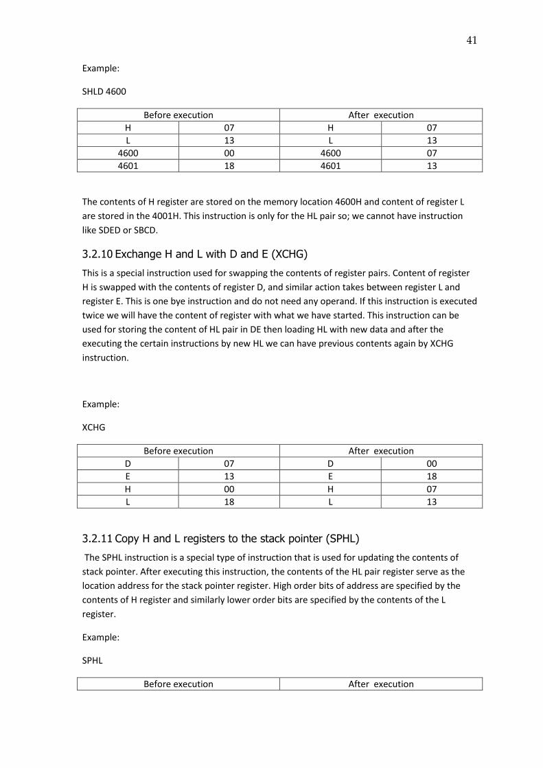
3.2.10 Exchange H and L with D and E (XCHG)
This is a special instruction used for swapping the contents of register pairs. Content of register
H is swapped with the contents of register D, and similar action takes between register L and
register E. This is one bye instruction and do not need any operand. If this instruction is executed
twice we will have the content of register with what we have started. This instruction can be
used for storing the content of HL pair in DE then loading HL with new data and after the
executing the certain instructions by new HL we can have previous contents again by XCHG
instruction.
Example:
XCHG
Before execution After execution
D 07 D 00
E 13 E 18
H 00 H 07
L 18 L 13
3.2.11 Copy H and L registers to the stack pointer (SPHL)
The SPHL instruction is a special type of instruction that is used for updating the contents of
stack pointer. After executing this instruction, the contents of the HL pair register serve as the
location address for the stack pointer register. High order bits of address are specified by the
contents of H register and similarly lower order bits are specified by the contents of the L
register.
Example:
SPHL
Before execution After execution
42
H 07 H 07
L 13 L 13
SP 8456 SP 0713
The content of HL register remains unaltered.
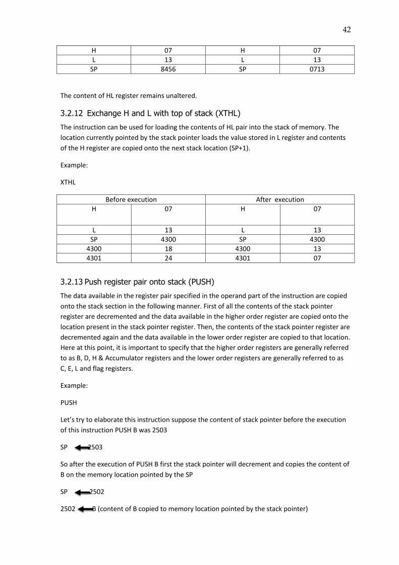
3.2.12 Exchange H and L with top of stack (XTHL)
The instruction can be used for loading the contents of HL pair into the stack of memory. The
location currently pointed by the stack pointer loads the value stored in L register and contents
of the H register are copied onto the next stack location (SP+1).
Example:
XTHL
Before execution After execution
H 07 H 07
L 13 L 13
SP 4300 SP 4300
4300 18 4300 13
4301 24 4301 07
3.2.13 Push register pair onto stack (PUSH)
The data available in the register pair specified in the operand part of the instruction are copied
onto the stack section in the following manner. First of all the contents of the stack pointer
register are decremented and the data available in the higher order register are copied onto the
location present in the stack pointer register. Then, the contents of the stack pointer register are
decremented again and the data available in the lower order register are copied to that location.
Here at this point, it is important to specify that the higher order registers are generally referred
to as B, D, H & Accumulator registers and the lower order registers are generally referred to as
C, E, L and flag registers.
Example:
PUSH
Let’s try to elaborate this instruction suppose the content of stack pointer before the execution
of this instruction PUSH B was 2503
SP 2503
So after the execution of PUSH B first the stack pointer will decrement and copies the content of
B on the memory location pointed by the SP
SP 2502
2502 B (content of B copied to memory location pointed by the stack pointer)
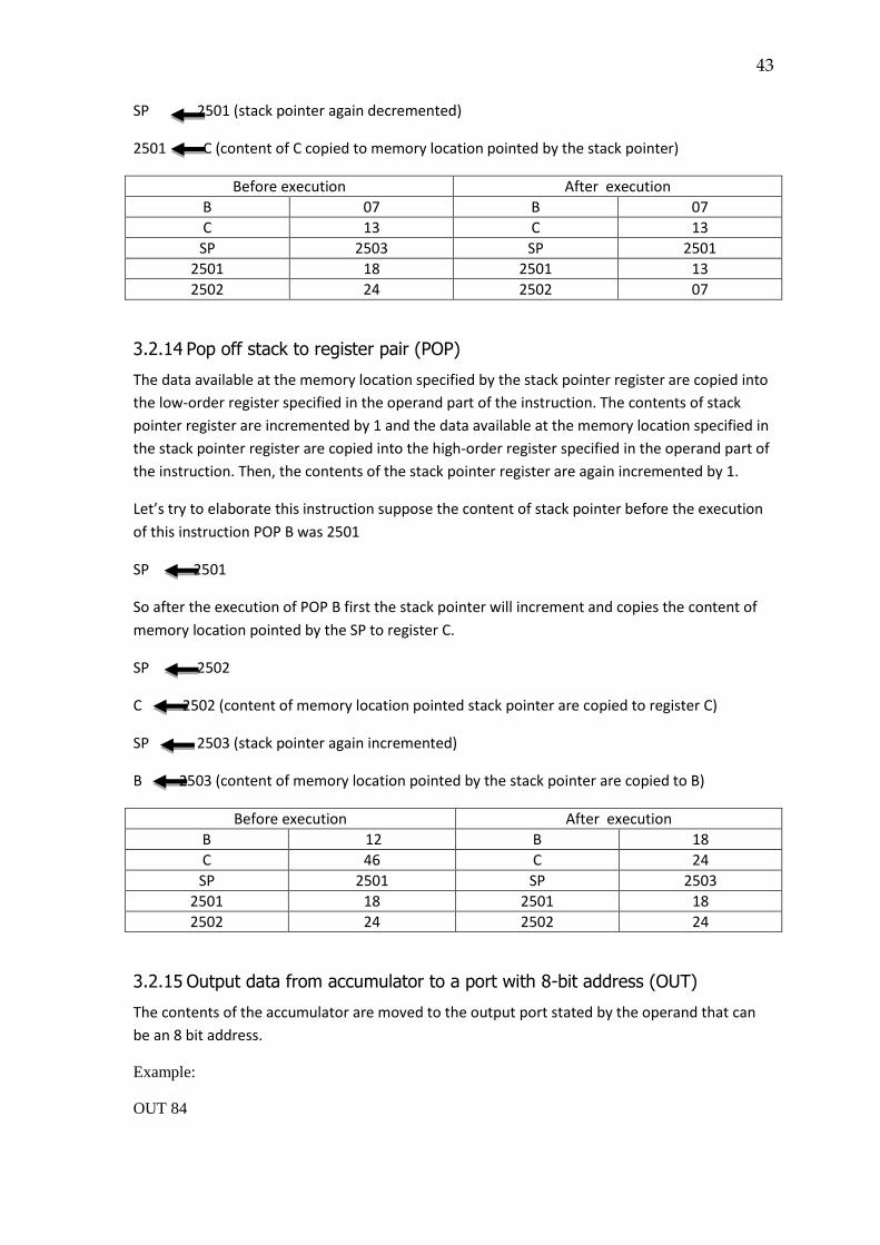
43
SP 2501 (stack pointer again decremented)
2501 C (content of C copied to memory location pointed by the stack pointer)
Before execution After execution
B 07 B 07
C 13 C 13
SP 2503 SP 2501
2501 18 2501 13
2502 24 2502 07
3.2.14 Pop off stack to register pair (POP)
The data available at the memory location specified by the stack pointer register are copied into
the low-order register specified in the operand part of the instruction. The contents of stack
pointer register are incremented by 1 and the data available at the memory location specified in
the stack pointer register are copied into the high-order register specified in the operand part of
the instruction. Then, the contents of the stack pointer register are again incremented by 1.
Let’s try to elaborate this instruction suppose the content of stack pointer before the execution
of this instruction POP B was 2501
SP 2501
So after the execution of POP B first the stack pointer will increment and copies the content of
memory location pointed by the SP to register C.
SP 2502
C 2502 (content of memory location pointed stack pointer are copied to register C)
SP 2503 (stack pointer again incremented)
B 2503 (content of memory location pointed by the stack pointer are copied to B)
Before execution After execution
B 12 B 18
C 46 C 24
SP 2501 SP 2503
2501 18 2501 18
2502 24 2502 24
3.2.15 Output data from accumulator to a port with 8-bit address (OUT)
The contents of the accumulator are moved to the output port stated by the operand that can
be an 8 bit address.
Example:
OUT 84
44
3.2.16 Input data to accumulator from a port with 8-bit address (IN)
The data from any external source can be read by the processor with the help of this instruction.
The external data at the ports of the processor can be entered into the accumulator by using IN
instruction. The operand contains single byte address of the port.
Example:
IN 83
Self-Assessment 1
Q1. Explain the term data transfer instruction for 8085.
Sol. ____________________________________________________________________
___________________________________________________________________________
_____________________________________________________________________________
_____________________________________________________________________________
Q2. How we can store data from accumulator to memory location directly?
Sol.__________________________________________________________________________
_____________________________________________________________________________
_____________________________________________________________________________
_____________________________________________________________________________
Q3. Explain the PUSH and POP instructions and their use.
Sol. ______________________________________________________________________
_____________________________________________________________________________
_____________________________________________________________________________
_____________________________________________________________________________
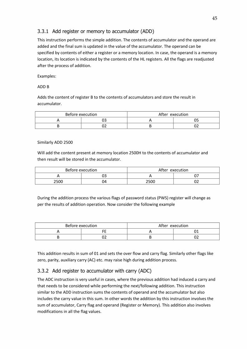
3.3 ARITHMETIC INSTRUCTIONS
The instructions of this group perform arithmetic operations such as addition, subtraction;
increment or decrement of the content of a register or memory. Athematic operations are
performed in the accumulators only. The operand data can be from the memory location or a
register. In 8085 8 bit arithmetic operations are allowed. If the operand is 16 bit the arithmetic
operation is performed in two steps by taking the carry flag into account.
Let’s consider the various types of arithmetic instructions along with examples.
45
3.3.1 Add register or memory to accumulator (ADD)
This instruction performs the simple addition. The contents of accumulator and the operand are
added and the final sum is updated in the value of the accumulator. The operand can be
specified by contents of either a register or a memory location. In case, the operand is a memory
location, its location is indicated by the contents of the HL registers. All the flags are readjusted
after the process of addition.
Examples:
ADD B
Adds the content of register B to the contents of accumulators and store the result in
accumulator.
Before execution After execution
A 03 A 05
B 02 B 02
Similarly ADD 2500
Will add the content present at memory location 2500H to the contents of accumulator and
then result will be stored in the accumulator.
Before execution After execution
A 03 A 07
2500 04 2500 02
During the addition process the various flags of password status (PWS) register will change as
per the results of addition operation. Now consider the following example
Before execution After execution
A FE A 01
B 02 B 02
This addition results in sum of 01 and sets the over flow and carry flag. Similarly other flags like
zero, parity, auxiliary carry (AC) etc. may raise high during addition process.
3.3.2 Add register to accumulator with carry (ADC)
The ADC instruction is very useful in cases, where the previous addition had induced a carry and
that needs to be considered while performing the next/following addition. This instruction
similar to the ADD instruction sums the contents of operand and the accumulator but also
includes the carry value in this sum. In other words the addition by this instruction involves the
sum of accumulator, Carry flag and operand (Register or Memory). This addition also involves
modifications in all the flag values.
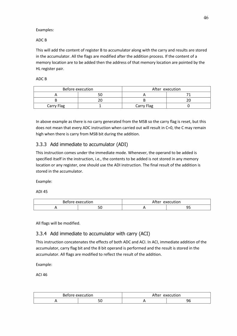
46
Examples:
ADC B
This will add the content of register B to accumulator along with the carry and results are stored
in the accumulator. All the flags are modified after the addition process. If the content of a
memory location are to be added then the address of that memory location are pointed by the
HL register pair.
ADC B
Before execution After execution
A 50 A 71
B 20 B 20
Carry Flag 1 Carry Flag 0
In above example as there is no carry generated from the MSB so the carry flag is reset, but this
does not mean that every ADC instruction when carried out will result in C=0, the C may remain
high when there is carry from MSB bit during the addition.
3.3.3 Add immediate to accumulator (ADI)
This instruction comes under the immediate mode. Whenever, the operand to be added is
specified itself in the instruction, i.e., the contents to be added is not stored in any memory
location or any register, one should use the ADI instruction. The final result of the addition is
stored in the accumulator.
Example:
ADI 45
Before execution After execution
A 50 A 95
All flags will be modified.
3.3.4 Add immediate to accumulator with carry (ACI)
This instruction concatenates the effects of both ADC and ACI. In ACI, immediate addition of the
accumulator, carry flag bit and the 8 bit operand is performed and the result is stored in the
accumulator. All flags are modified to reflect the result of the addition.
Example:
ACI 46
Before execution After execution
A 50 A 96
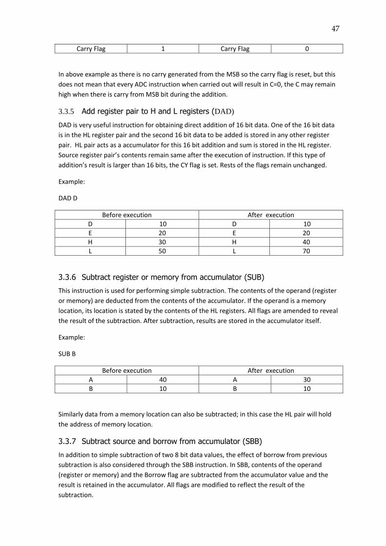
47
Carry Flag 1 Carry Flag 0
In above example as there is no carry generated from the MSB so the carry flag is reset, but this
does not mean that every ADC instruction when carried out will result in C=0, the C may remain
high when there is carry from MSB bit during the addition.
3.3.5 Add register pair to H and L registers (DAD)
DAD is very useful instruction for obtaining direct addition of 16 bit data. One of the 16 bit data
is in the HL register pair and the second 16 bit data to be added is stored in any other register
pair. HL pair acts as a accumulator for this 16 bit addition and sum is stored in the HL register.
Source register pair’s contents remain same after the execution of instruction. If this type of
addition’s result is larger than 16 bits, the CY flag is set. Rests of the flags remain unchanged.
Example:
DAD D
Before execution After execution
D 10 D 10
E 20 E 20
H 30 H 40
L 50 L 70
3.3.6 Subtract register or memory from accumulator (SUB)
This instruction is used for performing simple subtraction. The contents of the operand (register
or memory) are deducted from the contents of the accumulator. If the operand is a memory
location, its location is stated by the contents of the HL registers. All flags are amended to reveal
the result of the subtraction. After subtraction, results are stored in the accumulator itself.
Example:
SUB B
Before execution After execution
A 40 A 30
B 10 B 10
Similarly data from a memory location can also be subtracted; in this case the HL pair will hold
the address of memory location.
3.3.7 Subtract source and borrow from accumulator (SBB)
In addition to simple subtraction of two 8 bit data values, the effect of borrow from previous
subtraction is also considered through the SBB instruction. In SBB, contents of the operand
(register or memory) and the Borrow flag are subtracted from the accumulator value and the
result is retained in the accumulator. All flags are modified to reflect the result of the
subtraction.
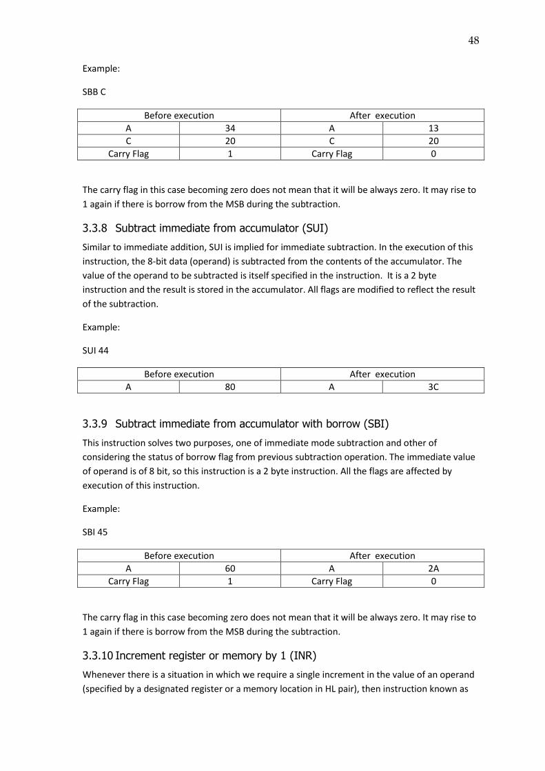
48
Example:
SBB C
Before execution After execution
A 34 A 13
C 20 C 20
Carry Flag 1 Carry Flag 0
The carry flag in this case becoming zero does not mean that it will be always zero. It may rise to
1 again if there is borrow from the MSB during the subtraction.
3.3.8 Subtract immediate from accumulator (SUI)
Similar to immediate addition, SUI is implied for immediate subtraction. In the execution of this
instruction, the 8-bit data (operand) is subtracted from the contents of the accumulator. The
value of the operand to be subtracted is itself specified in the instruction. It is a 2 byte
instruction and the result is stored in the accumulator. All flags are modified to reflect the result
of the subtraction.
Example:
SUI 44
Before execution After execution
A 80 A 3C
3.3.9 Subtract immediate from accumulator with borrow (SBI)
This instruction solves two purposes, one of immediate mode subtraction and other of
considering the status of borrow flag from previous subtraction operation. The immediate value
of operand is of 8 bit, so this instruction is a 2 byte instruction. All the flags are affected by
execution of this instruction.
Example:
SBI 45
Before execution After execution
A 60 A 2A
Carry Flag 1 Carry Flag 0
The carry flag in this case becoming zero does not mean that it will be always zero. It may rise to
1 again if there is borrow from the MSB during the subtraction.
3.3.10 Increment register or memory by 1 (INR)
Whenever there is a situation in which we require a single increment in the value of an operand
(specified by a designated register or a memory location in HL pair), then instruction known as
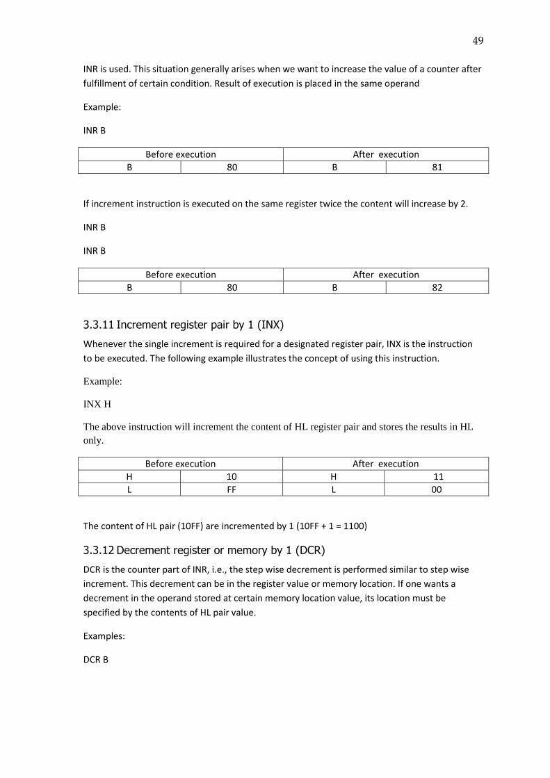
49
INR is used. This situation generally arises when we want to increase the value of a counter after
fulfillment of certain condition. Result of execution is placed in the same operand
Example:
INR B
Before execution After execution
B 80 B 81
If increment instruction is executed on the same register twice the content will increase by 2.
INR B
INR B
Before execution After execution
B 80 B 82
3.3.11 Increment register pair by 1 (INX)
Whenever the single increment is required for a designated register pair, INX is the instruction
to be executed. The following example illustrates the concept of using this instruction.
Example:
INX H
The above instruction will increment the content of HL register pair and stores the results in HL
only.
Before execution After execution
H 10 H 11
L FF L 00
The content of HL pair (10FF) are incremented by 1 (10FF + 1 = 1100)
3.3.12 Decrement register or memory by 1 (DCR)
DCR is the counter part of INR, i.e., the step wise decrement is performed similar to step wise
increment. This decrement can be in the register value or memory location. If one wants a
decrement in the operand stored at certain memory location value, its location must be
specified by the contents of HL pair value.
Examples:
DCR B
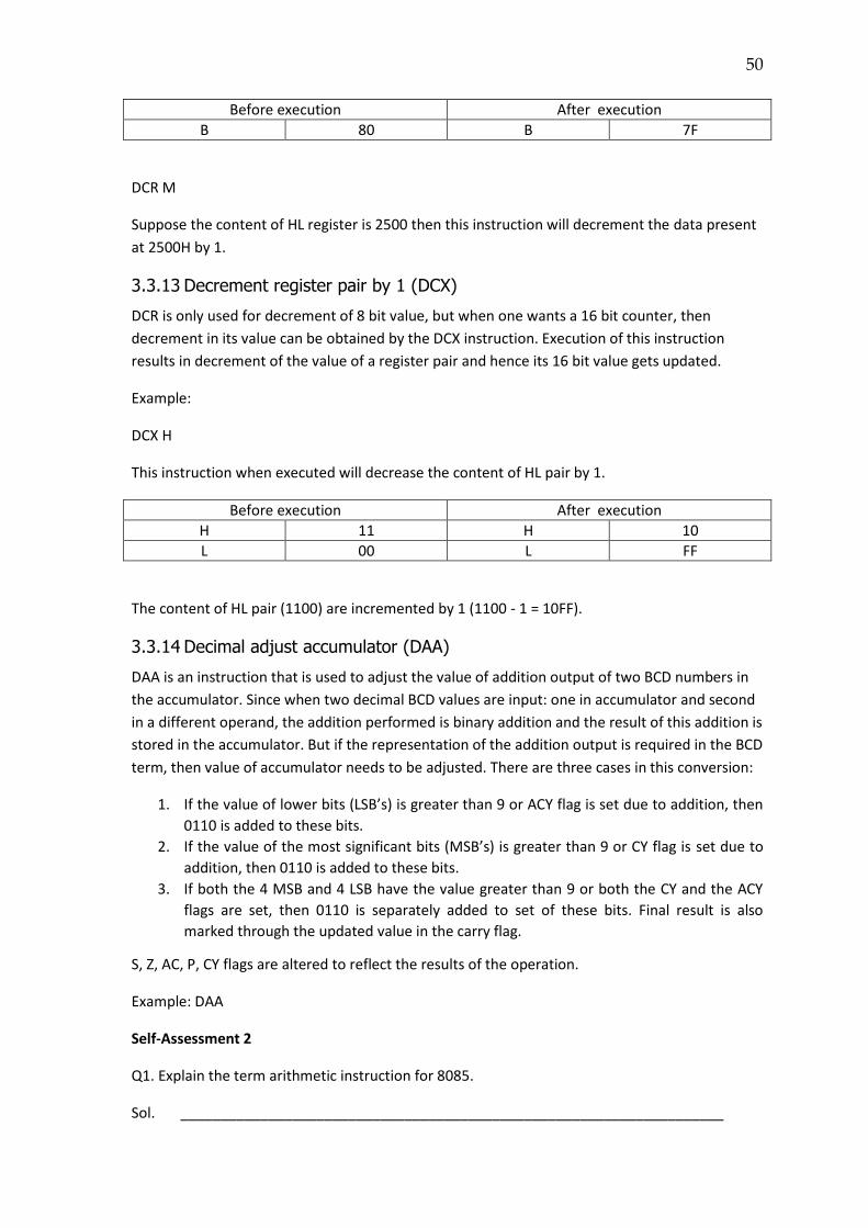
50
Before execution After execution
B 80 B 7F
DCR M
Suppose the content of HL register is 2500 then this instruction will decrement the data present
at 2500H by 1.
3.3.13 Decrement register pair by 1 (DCX)
DCR is only used for decrement of 8 bit value, but when one wants a 16 bit counter, then
decrement in its value can be obtained by the DCX instruction. Execution of this instruction
results in decrement of the value of a register pair and hence its 16 bit value gets updated.
Example:
DCX H
This instruction when executed will decrease the content of HL pair by 1.
Before execution After execution
H 11 H 10
L 00 L FF
The content of HL pair (1100) are incremented by 1 (1100 - 1 = 10FF).
3.3.14 Decimal adjust accumulator (DAA)
DAA is an instruction that is used to adjust the value of addition output of two BCD numbers in
the accumulator. Since when two decimal BCD values are input: one in accumulator and second
in a different operand, the addition performed is binary addition and the result of this addition is
stored in the accumulator. But if the representation of the addition output is required in the BCD
term, then value of accumulator needs to be adjusted. There are three cases in this conversion:
1. If the value of lower bits (LSB’s) is greater than 9 or ACY flag is set due to addition, then
0110 is added to these bits.
2. If the value of the most significant bits (MSB’s) is greater than 9 or CY flag is set due to
addition, then 0110 is added to these bits.
3. If both the 4 MSB and 4 LSB have the value greater than 9 or both the CY and the ACY
flags are set, then 0110 is separately added to set of these bits. Final result is also
marked through the updated value in the carry flag.
S, Z, AC, P, CY flags are altered to reflect the results of the operation.
Example: DAA
Self-Assessment 2
Q1. Explain the term arithmetic instruction for 8085.
Sol. ____________________________________________________________________
51
___________________________________________________________________________
_____________________________________________________________________________
_____________________________________________________________________________
Q2. How one can perform the 16 bit addition with carry?
Sol.__________________________________________________________________________
_____________________________________________________________________________
_____________________________________________________________________________
_____________________________________________________________________________
Q3. Explain the DAA instruction and its use.
Sol. ______________________________________________________________________
_____________________________________________________________________________
_____________________________________________________________________________
________________________________________________________________________
3.4 Logical Instructions
This type of instructions fall into category when one wants to perform a logic based function on
the operand. The various logical functions include Boolean AND, OR, XOR, compare conditions
and rotate instructions etc. The operands to be operated under this type of instructions must be
specified by the combinations of either two register operands or a general register operand with
a memory operand.
3.4.1 Compare register or memory with accumulator (CMP)
Comparison of the value present in accumulator register with the second operand value
specified either through register or memory location is done with the help of this instruction.
The output of comparison is indicated through the PSW flags for following cases:
if (A) < (reg/mem): carry flag (CF) is set, s = 1
if (A) = (reg/mem): zero flag (ZF) is set, s = 0
if (A) > (reg/mem): carry and zero flags are reset, s = 0
Example:
CMP B
Before execution After execution
A 10 A 10
B 20 B 20
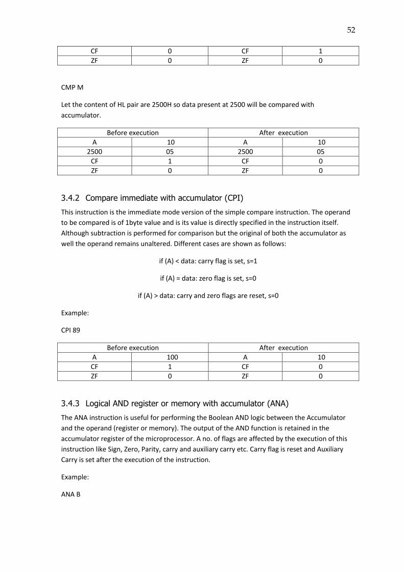
52
CF 0 CF 1
ZF 0 ZF 0
CMP M
Let the content of HL pair are 2500H so data present at 2500 will be compared with
accumulator.
Before execution After execution
A 10 A 10
2500 05 2500 05
CF 1 CF 0
ZF 0 ZF 0
3.4.2 Compare immediate with accumulator (CPI)
This instruction is the immediate mode version of the simple compare instruction. The operand
to be compared is of 1byte value and is its value is directly specified in the instruction itself.
Although subtraction is performed for comparison but the original of both the accumulator as
well the operand remains unaltered. Different cases are shown as follows:
if (A) < data: carry flag is set, s=1
if (A) = data: zero flag is set, s=0
if (A) > data: carry and zero flags are reset, s=0
Example:
CPI 89
Before execution After execution
A 100 A 10
CF 1 CF 0
ZF 0 ZF 0
3.4.3 Logical AND register or memory with accumulator (ANA)
The ANA instruction is useful for performing the Boolean AND logic between the Accumulator
and the operand (register or memory). The output of the AND function is retained in the
accumulator register of the microprocessor. A no. of flags are affected by the execution of this
instruction like Sign, Zero, Parity, carry and auxiliary carry etc. Carry flag is reset and Auxiliary
Carry is set after the execution of the instruction.
Example:
ANA B
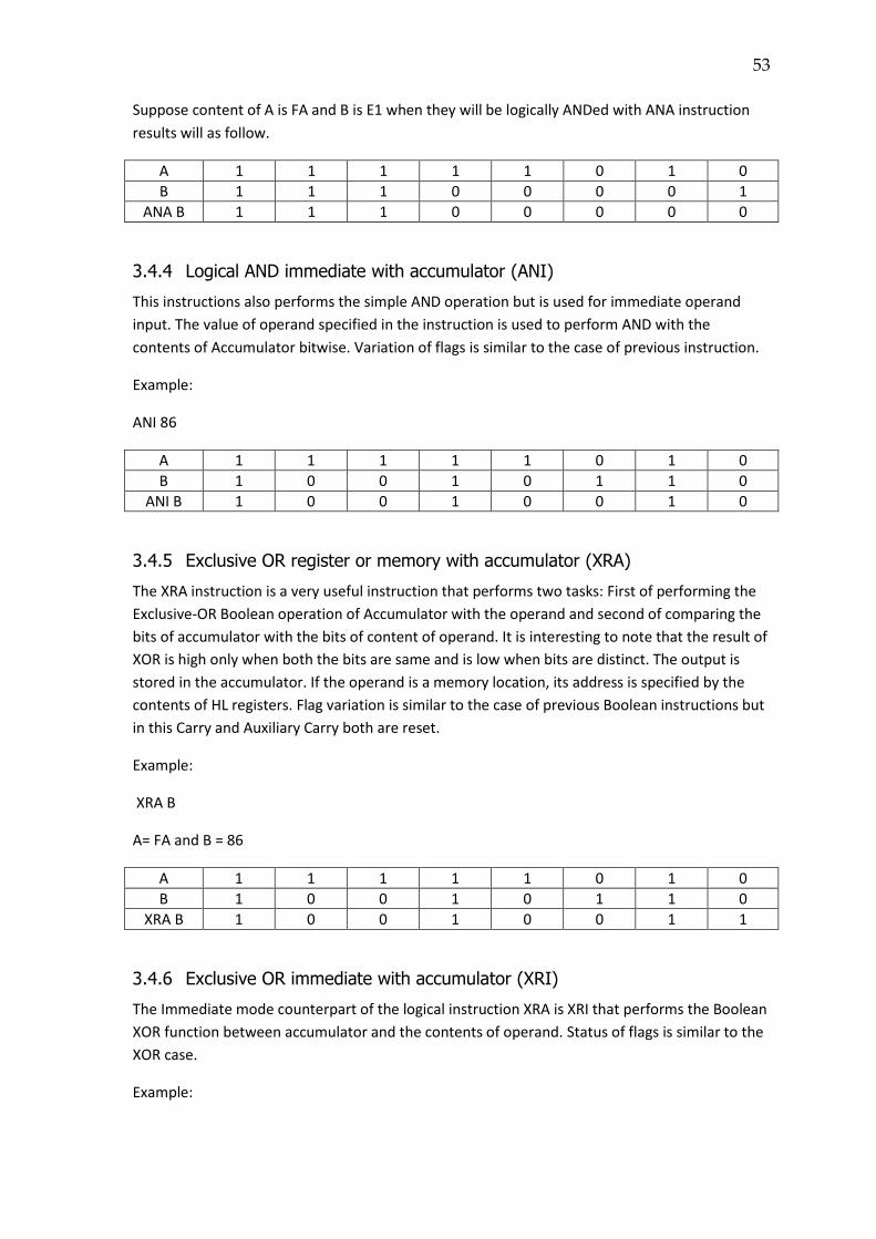
53
Suppose content of A is FA and B is E1 when they will be logically ANDed with ANA instruction
results will as follow.
A 1 1 1 1 1 0 1 0
B 1 1 1 0 0 0 0 1
ANA B 1 1 1 0 0 0 0 0
3.4.4 Logical AND immediate with accumulator (ANI)
This instructions also performs the simple AND operation but is used for immediate operand
input. The value of operand specified in the instruction is used to perform AND with the
contents of Accumulator bitwise. Variation of flags is similar to the case of previous instruction.
Example:
ANI 86
A 1 1 1 1 1 0 1 0
B 1 0 0 1 0 1 1 0
ANI B 1 0 0 1 0 0 1 0
3.4.5 Exclusive OR register or memory with accumulator (XRA)
The XRA instruction is a very useful instruction that performs two tasks: First of performing the
Exclusive-OR Boolean operation of Accumulator with the operand and second of comparing the
bits of accumulator with the bits of content of operand. It is interesting to note that the result of
XOR is high only when both the bits are same and is low when bits are distinct. The output is
stored in the accumulator. If the operand is a memory location, its address is specified by the
contents of HL registers. Flag variation is similar to the case of previous Boolean instructions but
in this Carry and Auxiliary Carry both are reset.
Example:
XRA B
A= FA and B = 86
A 1 1 1 1 1 0 1 0
B 1 0 0 1 0 1 1 0
XRA B 1 0 0 1 0 0 1 1
3.4.6 Exclusive OR immediate with accumulator (XRI)
The Immediate mode counterpart of the logical instruction XRA is XRI that performs the Boolean
XOR function between accumulator and the contents of operand. Status of flags is similar to the
XOR case.
Example:
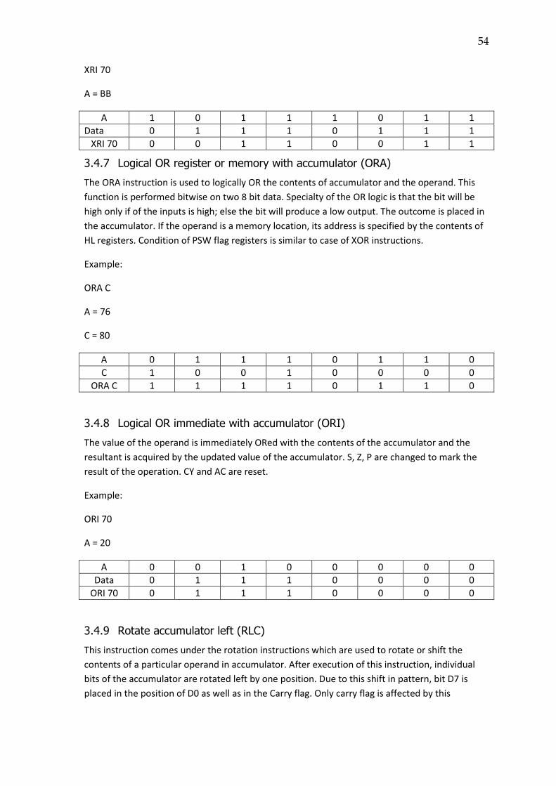
54
XRI 70
A = BB
A 1 0 1 1 1 0 1 1
Data 0 1 1 1 0 1 1 1
XRI 70 0 0 1 1 0 0 1 1
3.4.7 Logical OR register or memory with accumulator (ORA)
The ORA instruction is used to logically OR the contents of accumulator and the operand. This
function is performed bitwise on two 8 bit data. Specialty of the OR logic is that the bit will be
high only if of the inputs is high; else the bit will produce a low output. The outcome is placed in
the accumulator. If the operand is a memory location, its address is specified by the contents of
HL registers. Condition of PSW flag registers is similar to case of XOR instructions.
Example:
ORA C
A = 76
C = 80
A 0 1 1 1 0 1 1 0
C 1 0 0 1 0 0 0 0
ORA C 1 1 1 1 0 1 1 0
3.4.8 Logical OR immediate with accumulator (ORI)
The value of the operand is immediately ORed with the contents of the accumulator and the
resultant is acquired by the updated value of the accumulator. S, Z, P are changed to mark the
result of the operation. CY and AC are reset.
Example:
ORI 70
A = 20
A 0 0 1 0 0 0 0 0
Data 0 1 1 1 0 0 0 0
ORI 70 0 1 1 1 0 0 0 0
3.4.9 Rotate accumulator left (RLC)
This instruction comes under the rotation instructions which are used to rotate or shift the
contents of a particular operand in accumulator. After execution of this instruction, individual
bits of the accumulator are rotated left by one position. Due to this shift in pattern, bit D7 is
placed in the position of D0 as well as in the Carry flag. Only carry flag is affected by this
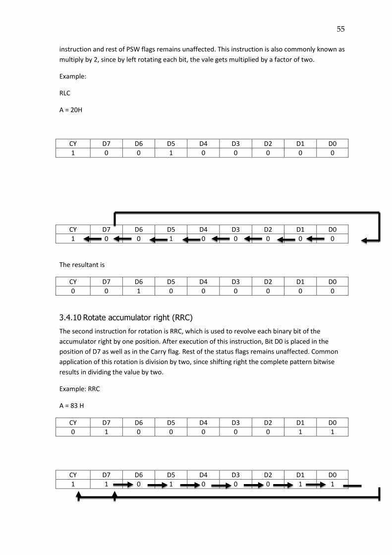
55
instruction and rest of PSW flags remains unaffected. This instruction is also commonly known as
multiply by 2, since by left rotating each bit, the vale gets multiplied by a factor of two.
Example:
RLC
A = 20H
CY D7 D6 D5 D4 D3 D2 D1 D0
1 0 0 1 0 0 0 0 0
CY D7 D6 D5 D4 D3 D2 D1 D0
1 0 0 1 0 0 0 0 0
The resultant is
CY D7 D6 D5 D4 D3 D2 D1 D0
0 0 1 0 0 0 0 0 0
3.4.10 Rotate accumulator right (RRC)
The second instruction for rotation is RRC, which is used to revolve each binary bit of the
accumulator right by one position. After execution of this instruction, Bit D0 is placed in the
position of D7 as well as in the Carry flag. Rest of the status flags remains unaffected. Common
application of this rotation is division by two, since shifting right the complete pattern bitwise
results in dividing the value by two.
Example: RRC
A = 83 H
CY D7 D6 D5 D4 D3 D2 D1 D0
0 1 0 0 0 0 0 1 1
CY D7 D6 D5 D4 D3 D2 D1 D0
1 1 0 1 0 0 0 1 1
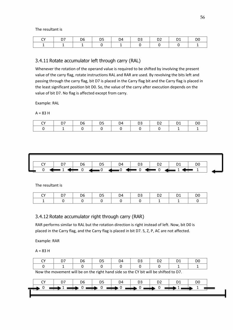
56
The resultant is
CY D7 D6 D5 D4 D3 D2 D1 D0
1 1 1 0 1 0 0 0 1
3.4.11 Rotate accumulator left through carry (RAL)
Whenever the rotation of the operand value is required to be shifted by involving the present
value of the carry flag, rotate instructions RAL and RAR are used. By revolving the bits left and
passing through the carry flag, bit D7 is placed in the Carry flag bit and the Carry flag is placed in
the least significant position bit D0. So, the value of the carry after execution depends on the
value of bit D7. No flag is affected except from carry.
Example: RAL
A = 83 H
CY D7 D6 D5 D4 D3 D2 D1 D0
0 1 0 0 0 0 0 1 1
CY D7 D6 D5 D4 D3 D2 D1 D0
0 1 0 0 0 0 0 1 1
The resultant is
CY D7 D6 D5 D4 D3 D2 D1 D0
1 0 0 0 0 0 1 1 0
3.4.12 Rotate accumulator right through carry (RAR)
RAR performs similar to RAL but the rotation direction is right instead of left. Now, bit D0 is
placed in the Carry flag, and the Carry flag is placed in bit D7. S, Z, P, AC are not affected.
Example: RAR
A = 83 H
CY D7 D6 D5 D4 D3 D2 D1 D0
0 1 0 0 0 0 0 1 1
Now the movement will be on the right hand side so the CY bit will be shifted to D7.
CY D7 D6 D5 D4 D3 D2 D1 D0
0 1 0 0 0 0 0 1 1
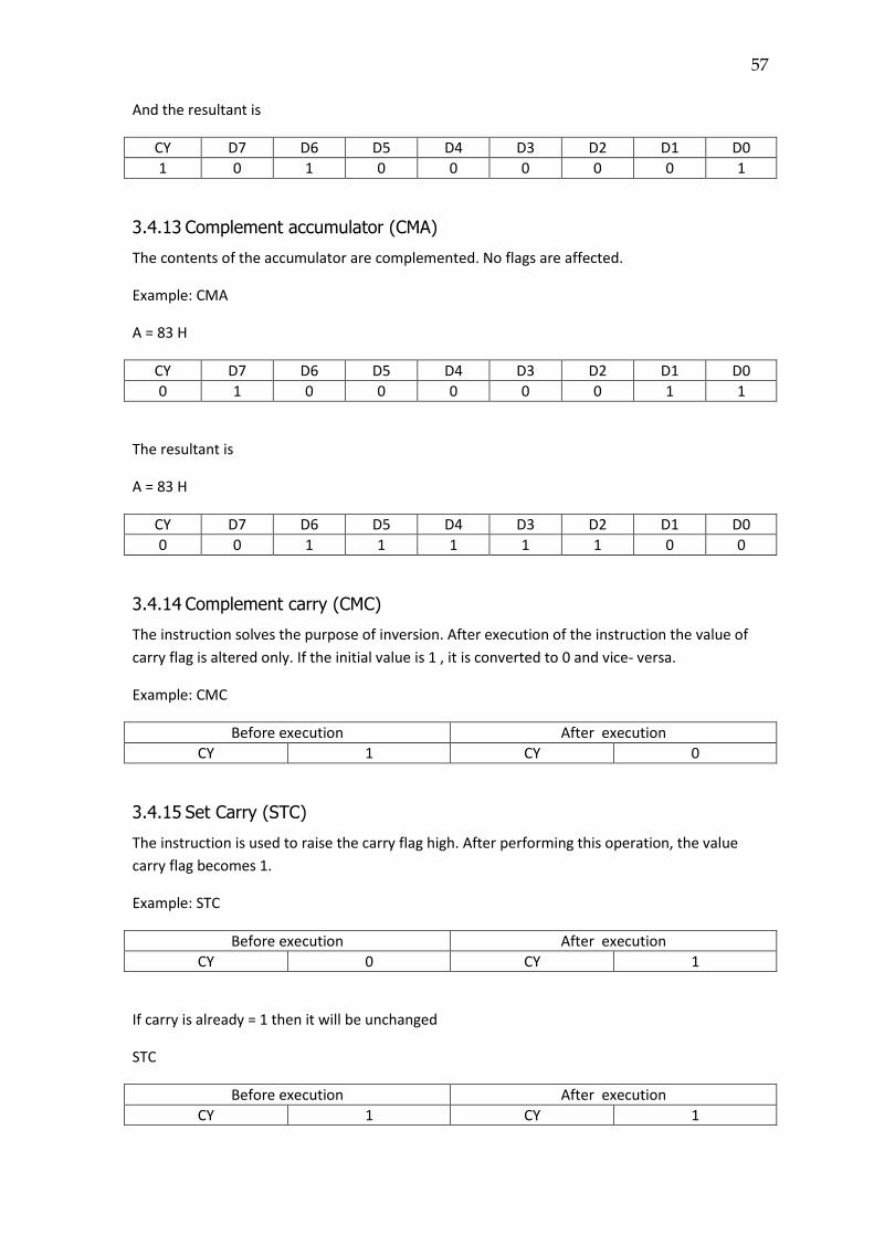
57
And the resultant is
CY D7 D6 D5 D4 D3 D2 D1 D0
1 0 1 0 0 0 0 0 1
3.4.13 Complement accumulator (CMA)
The contents of the accumulator are complemented. No flags are affected.
Example: CMA
A = 83 H
CY D7 D6 D5 D4 D3 D2 D1 D0
0 1 0 0 0 0 0 1 1
The resultant is
A = 83 H
CY D7 D6 D5 D4 D3 D2 D1 D0
0 0 1 1 1 1 1 0 0
3.4.14 Complement carry (CMC)
The instruction solves the purpose of inversion. After execution of the instruction the value of
carry flag is altered only. If the initial value is 1 , it is converted to 0 and vice- versa.
Example: CMC
Before execution After execution
CY 1 CY 0
3.4.15 Set Carry (STC)
The instruction is used to raise the carry flag high. After performing this operation, the value
carry flag becomes 1.
Example: STC
Before execution After execution
CY 0 CY 1
If carry is already = 1 then it will be unchanged
STC
Before execution After execution
CY 1 CY 1
58
3.5 Branch Group Instructions
This group includes the instructions are most powerful instruction for a computer because they
can change the sequence of a program either unconditionally or with some conditions. They are
key to flexibility and versatility of a computer program. The microprocessor is a sequential
program it executes the instructions in sequence the branch instructions instruct the computer
to execute from a different location. They can be divided into following categories.
Jump Instructions
Call and Return instructions
Restart instructions
3.5.1 Jump unconditionally (JMP)
This instruction is used when the control of execution is to be shifted to some particular location
instantly without waiting for any particular condition to be fulfilled. The location to be jumped to
is provided by the 16-bit address given in the operand.
Example:JMP 2010
This instruction will force the microprocessor to execute from the 2034H location.
3.5.2 Jump conditionally
As the name suggests, Jump Conditionally is the instruction which is used to jump to particular
memory location specified by the operand on the fulfillment of a certain condition. And the
satisfaction of the condition is shown through the status of some PSW flags which is listed below
in the following table:
Opcode Description Flag Status JC Jump on Carry CY = 1
JNC Jump if No Carry CY = 0
JP Jump on Positive S = 0
JM Jump on Minus S = 1
JZ Jump if Zero Z = 1
JNZ Jump if Not Zero Z = 0
JPE Jump if Even Parity P = 1
JPO Jump if Odd parity P = 0
Let’s try to understand the above instructions with some examples
Example:Load the hexadecimal 20H and 35H number in D and E register respectively. If the
number is greater than the FFH display 01H at PORT0 otherwise display results.
Problem analysis and flow chart
This problem can be divided into the following sections
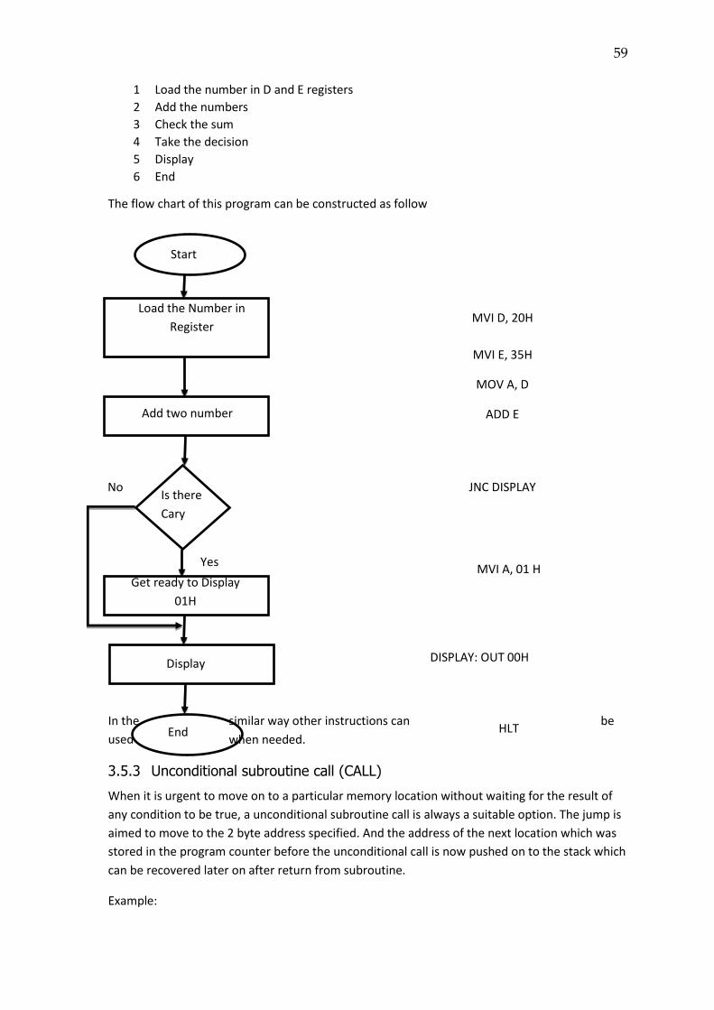
59
1 Load the number in D and E registers
2 Add the numbers
3 Check the sum
4 Take the decision
5 Display
6 End
The flow chart of this program can be constructed as follow
In the similar way other instructions can be
used when needed.
3.5.3 Unconditional subroutine call (CALL)
When it is urgent to move on to a particular memory location without waiting for the result of
any condition to be true, a unconditional subroutine call is always a suitable option. The jump is
aimed to move to the 2 byte address specified. And the address of the next location which was
stored in the program counter before the unconditional call is now pushed on to the stack which
can be recovered later on after return from subroutine.
Example:
Start
Load the Number in
Register
Add two number
Is there
Cary
Yes
No
Get ready to Display
01H
Display
End
MVI D, 20H
MVI E, 35H
MOV A, D
ADD E
JNC DISPLAY
DISPLAY: OUT 00H
MVI A, 01 H
HLT
60
CALL 2020
Note that the call instruction is always associated with the RET otherwise call will be just like an
unconditional JUMP instruction only. The above instruction when executed will force the
microprocessor to push the content of instruction pointer to the stack register and loading
instruction pointer with 2020H so, that microprocessor starts executing from the 2020H when
return instruction is encountered the program counter regains the stacked content and starts
executing exactly from where it has left.
3.5.4 Call conditionally
In these instructions the call is made when some desired condition is observed for example one
wants to execute certain subroutine when there is carry or the results are negative etc. The
following table shows the status of various flags and call formats. Every opcode is followed by
the 16 bit address.
Opcode Description Flag Status CC Call on Carry CY = 1
CNC Call if No Carry CY = 0
CP Call on Positive S = 0
CM Call on Minus S = 1
CZ Call if Zero Z = 1
CNZ Call if Not Zero Z = 0
CPE Call if Even Parity P = 1
CPO Call if Odd parity P = 0
3.5.5 Return from subroutine unconditionally (RET)
Whenever this command/ instruction occur within the microprocessor program the sequence of
the program is shifted from the sub-routine to the main calling program. Top two byte contents
of the stack are copied to the PC (Program Counter). Then, the program starts executing from
the new location/address.
Example:
RET
3.5.6 Return from subroutine conditionally
Sometimes, there is a situation that the subroutine must be exited only when some certain
condition is fulfilled. The exit stage is not fixed and varies depending on certain flag values.
These flags that mark themselves according to the result obtained from previous instructions.
The stack and the program counter strategies are similar to the previous return case. The
different cases for conditional return are mentioned below:
Opcode Description Flag Status RC Return on Carry CY = 1
RNC Return if No Carry CY = 0
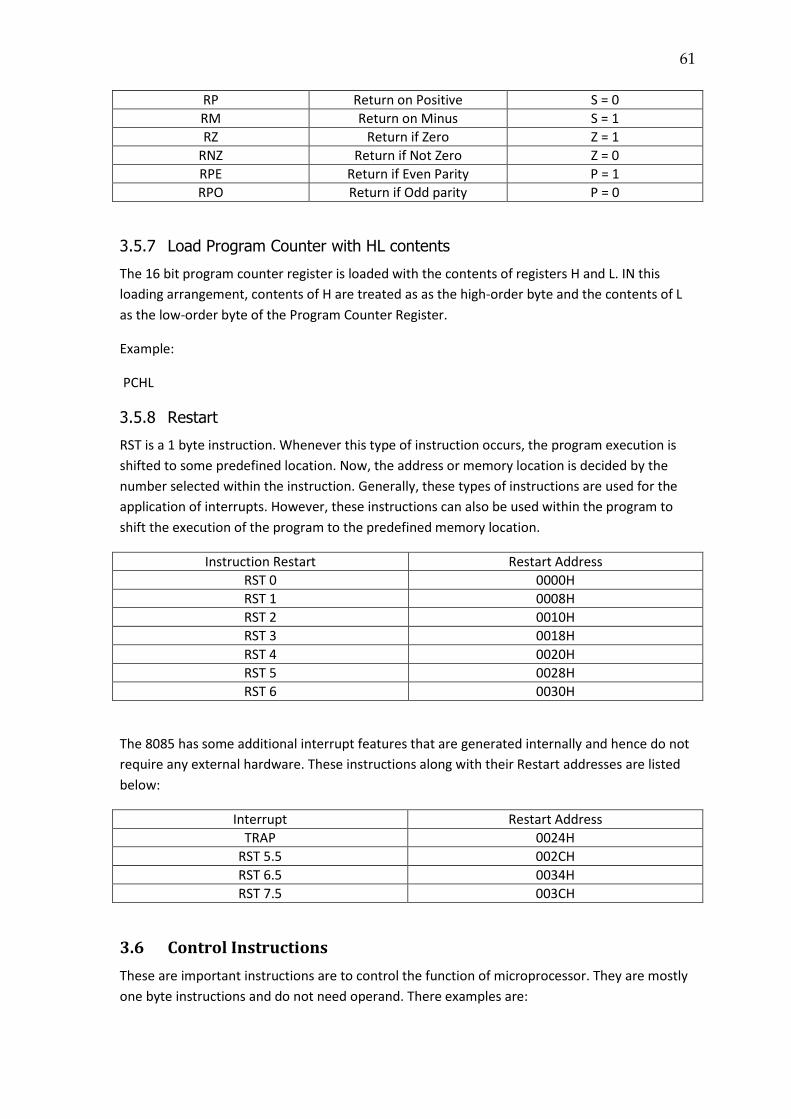
61
RP Return on Positive S = 0
RM Return on Minus S = 1
RZ Return if Zero Z = 1
RNZ Return if Not Zero Z = 0
RPE Return if Even Parity P = 1
RPO Return if Odd parity P = 0
3.5.7 Load Program Counter with HL contents
The 16 bit program counter register is loaded with the contents of registers H and L. IN this
loading arrangement, contents of H are treated as as the high-order byte and the contents of L
as the low-order byte of the Program Counter Register.
Example:
PCHL
3.5.8 Restart
RST is a 1 byte instruction. Whenever this type of instruction occurs, the program execution is
shifted to some predefined location. Now, the address or memory location is decided by the
number selected within the instruction. Generally, these types of instructions are used for the
application of interrupts. However, these instructions can also be used within the program to
shift the execution of the program to the predefined memory location.
Instruction Restart Restart Address
RST 0 0000H
RST 1 0008H
RST 2 0010H
RST 3 0018H
RST 4 0020H
RST 5 0028H
RST 6 0030H
The 8085 has some additional interrupt features that are generated internally and hence do not
require any external hardware. These instructions along with their Restart addresses are listed
below:
Interrupt Restart Address
TRAP 0024H
RST 5.5 002CH
RST 6.5 0034H
RST 7.5 003CH
3.6 Control Instructions
These are important instructions are to control the function of microprocessor. They are mostly
one byte instructions and do not need operand. There examples are:
62
3.6.1 No operation (NOP)
No operation is performed. The instruction is fetched and decoded. However no operation is
executed.
Example:
NOP
3.6.2 Halt and enter wait state (HLT)
The CPU afterfinishing the execution the current instruction stops performing any further
execution. In other words, the processor stand stills until an interrupt or reset is invoked to exit
the current halt state.
Example:
HLT
3.6.3 Disable interrupts (DI)
This instruction is executed to stop the action of interrupts applied. TRAP is excluded from the
effect of this command. Enable interrupt is reset but rest of the Flags remain unaffected.
Example:
DI
3.6.4 Enable interrupts (EI)
Setting the enable interrupt flip flop through instruction EI results in enabling all the interrupts.
So, before calling any interrupt subroutine, it is important to first enable them. Enabling
processing is just like opening the locked door with a key to further proceed for rest of the
operation. In enabling operation no flags are affected. This flip flop can be reset when one wants
to disable the interrupts. It can be reset after a system reset or the acknowledgement of an
interrupt. Only TRAP interrupt is exempted from the allowance using EI.
Example:
EI
63
Chapter 4
Addressing Mode
Structure
4.0 Objectives
4.1 Introduction
4.2 Operand and Opcode
4.3 Classification of addressing modes
4.4 Direct Addressing Mode
4.5 Indirect Addressing Mode
4.6 Register Addressing Mode
4.7 Immediate Addressing Mode
4.8 Implicit Addressing Mode
4.9 Summary
4.10 Glossary
4.11 Answer to Check Your Progress/Suggested Answers to SAQ
4.12 Bibliography/References/ Suggested Readings
4.13 Terminal and Model Questions
4.0 Objectives
After studying this chapter one will understand
What is opcode and operand?
How to access the data from memory or registers?
Definition of Addressing mode
Different types of addressing modes,
Basic concepts of Direct, Indirect, register, immediate and implicit addressing mode
Use of addressing modes in different conditions.
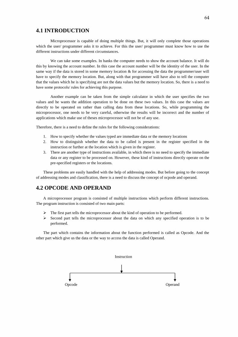
64
4.1 INTRODUCTION
Microprocessor is capable of doing multiple things. But, it will only complete those operations
which the user/ programmer asks it to achieve. For this the user/ programmer must know how to use the
different instructions under different circumstances.
We can take some examples. In banks the computer needs to show the account balance. It will do
this by knowing the account number. In this case the account number will be the identity of the user. In the
same way if the data is stored in some memory location & for accessing the data the programmer/user will
have to specify the memory location. But, along with that programmer will have also to tell the computer
that the values which he is specifying are not the data values but the memory location. So, there is a need to
have some protocols/ rules for achieving this purpose.
Another example can be taken from the simple calculator in which the user specifies the two
values and he wants the addition operation to be done on these two values. In this case the values are
directly to be operated on rather than calling data from these locations. So, while programming the
microprocessor, one needs to be very careful, otherwise the results will be incorrect and the number of
applications which make use of theses microprocessor will not be of any use.
Therefore, there is a need to define the rules for the following considerations:
1. How to specify whether the values typed are immediate data or the memory locations
2. How to distinguish whether the data to be called is present in the register specified in the
instruction or further at the location which is given in the register.
3. There are another type of instructions available, in which there is no need to specify the immediate
data or any register to be processed on. However, these kind of instructions directly operate on the
pre-specified registers or the locations.
These problems are easily handled with the help of addressing modes. But before going to the concept
of addressing modes and classification, there is a need to discuss the concept of ocpode and operand.
4.2 OPCODE AND OPERAND
A microprocessor program is consisted of multiple instructions which perform different instructions.
The program instruction is consisted of two main parts:
The first part tells the microprocessor about the kind of operation to be performed.
Second part tells the microprocessor about the data on which any specified operation is to be
performed.
The part which contains the information about the function performed is called as Opcode. And the
other part which give us the data or the way to access the data is called Operand.
Instruction
Opcode Operand
65
Addressing Modes
There is a method of specifying the data to be operated on by some microprocessor instruction.. The
method by whichthe instructions address the data to be processed (operated on)is known as addressing.
And the ways of identifying the operand for some particular task/instruction by the microprocessor are
known as Addressing modes. In other words, the manner in which the target address or effective address are
identified within the instruction is called addressing mode.
Self Assessment 1
Q1. What is Opcode? Explain with suitable example.
Sol. _____________________________________________________
_____________________________________________________
_____________________________________________________
_____________________________________________________
_____________________________________________________
Q2. Whatis Operand? Explain with suitable example.
Sol. _____________________________________________________
_____________________________________________________
_____________________________________________________
_____________________________________________________
_____________________________________________________
Q3. Define Addressing Mode. What is its need?
Sol. _____________________________________________________
_____________________________________________________
_____________________________________________________
_____________________________________________________
_____________________________________________________
4.3 CLASSIFICATION OF ADDRESSING MODES
We can identify the process to be operated upon the operands based on thegiven instructionin different
ways. Generally, the following addressing modes are used in 8085 microprocessor.
1. Direct addressing mode.
2. Indirect addressing mode
3. Register addressing mode
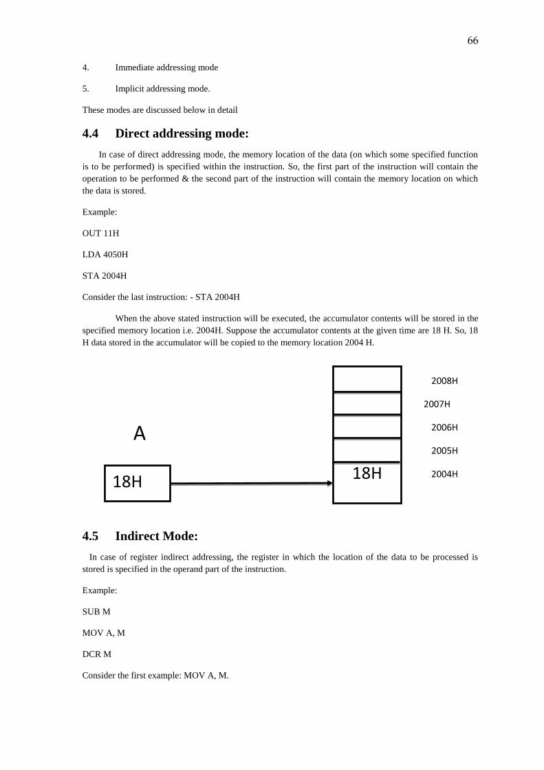
66
4. Immediate addressing mode
5. Implicit addressing mode.
These modes are discussed below in detail
4.4 Direct addressing mode:
In case of direct addressing mode, the memory location of the data (on which some specified function
is to be performed) is specified within the instruction. So, the first part of the instruction will contain the
operation to be performed & the second part of the instruction will contain the memory location on which
the data is stored.
Example:
OUT 11H
LDA 4050H
STA 2004H
Consider the last instruction: - STA 2004H
When the above stated instruction will be executed, the accumulator contents will be stored in the
specified memory location i.e. 2004H. Suppose the accumulator contents at the given time are 18 H. So, 18
H data stored in the accumulator will be copied to the memory location 2004 H.
4.5 Indirect Mode:
In case of register indirect addressing, the register in which the location of the data to be processed is
stored is specified in the operand part of the instruction.
Example:
SUB M
MOV A, M
DCR M
Consider the first example: MOV A, M.
18H
18H
A 2008H
2007H
2006H
2005H
2004H
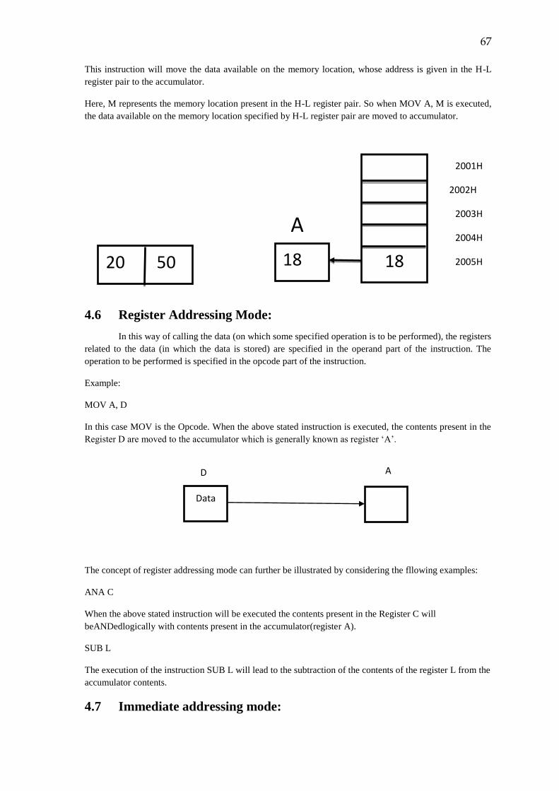
67
This instruction will move the data available on the memory location, whose address is given in the H-L
register pair to the accumulator.
Here, M represents the memory location present in the H-L register pair. So when MOV A, M is executed,
the data available on the memory location specified by H-L register pair are moved to accumulator.
4.6 Register Addressing Mode:
In this way of calling the data (on which some specified operation is to be performed), the registers
related to the data (in which the data is stored) are specified in the operand part of the instruction. The
operation to be performed is specified in the opcode part of the instruction.
Example:
MOV A, D
In this case MOV is the Opcode. When the above stated instruction is executed, the contents present in the
Register D are moved to the accumulator which is generally known as register ‘A’.
The concept of register addressing mode can further be illustrated by considering the fllowing examples:
ANA C
When the above stated instruction will be executed the contents present in the Register C will
beANDedlogically with contents present in the accumulator(register A).
SUB L
The execution of the instruction SUB L will lead to the subtraction of the contents of the register L from the
accumulator contents.
4.7 Immediate addressing mode:
20 50 18
18
A 2001H
2002H
2003H
2004H
2005H
Data
D A
68
In the case of immediate addressing, the data to be processed itself is specified in the operand part of the
instruction. In the opcode part, the operation to be performed is specified. Now, based o these two things
the microprocessor will accomplish the given task .It is the simple way of getting things done where we are
providing both the things: the function to be performed and the data on which the function is to be
performed.
Consider the following example:
ADI 34H – This instruction adds the immediate data, 34H to the accumulator.
Suppose, the contents of the accumulator register at present are 8H. When the instruction ‘ADI 34H’ will be
executed, 34H will be added to 8H and the final result will be stored in accumulator.
In the above instruction the operand is specified within instruction itself.
4.8 Implicit mode:
In this case, there is no need to type/write any register, data or memory location. The data is automatically
fetched from the predefined location according to the instruction used/typed. Generally, this type of the
addressing mode is used when there is a need to operate on the data available in the accumulator only.
Example:
CMA
RAL
RAR
CMA complements the contents of accumulator.
If RAL is executed the contents of accumulator is rotated left one bit through carry.
If RAR is executed the contents of accumulator is rotated right one bit through carry.
Self Assessment 2
Q1.Explain and classify addressing modes.
Sol. _____________________________________________________
_____________________________________________________
_____________________________________________________
_____________________________________________________
_____________________________________________________
Q2. What is the difference between direct and indirect addressing mode?
Sol. _____________________________________________________
_____________________________________________________
_____________________________________________________
_____________________________________________________
_____________________________________________________
69
Q3. Explain implicit addressing mode. How is it different from all of the other addressing modes?
Sol. _____________________________________________________
_____________________________________________________
_____________________________________________________
_____________________________________________________
_____________________________________________________
Q4. Explain how the presence of operand effects the size of any given instruction?
Sol. _____________________________________________________
_____________________________________________________
_____________________________________________________
_____________________________________________________
_____________________________________________________
The five addressing modes can be very easily understood with the help of the following table which
summarizes some of the examples of the addressing modes.
TYPE INSTRUCTION
Direct STA 2005H
Indirect MOV A,M
Register MOV A,B
Immediate MVI A, 18H
Implicit CMA
Self Assessment 3
In the following instructions find out the addressing mode applied.
Accumulator Memory
2005H
Accumulator Memory [[HL]]
Register B Accumulator
Data 18H Accumulator
Source Destination
70
Q1.LXI B, 2700H __________________________________
Q2.LDA 4000H __________________________________
Q3.DAA __________________________________
Q4.ADD B __________________________________
Q5.MOV M, A __________________________________
Self Assessment 4
Q1. OPCODE is a ________________________
(a) That part of instruction which tells the computer what operation to perform
(b) An auxiliary register that stores the data to be added or subtracted from the accumulator.
(c) The register that receives the information from the memory.
(d) One of the instruction in the instruction set.
Q2. Addressing in which the instruction contains the address of the data to be operated on, is known
as______________________________
(a) Immediate addressing
(b) Direct addressing
(c) Implicit addressing
(d) Register addressing
Q3. Which addressing mode is used in DAA? ____________________
(a) Implicit
(b) direct
(c) indirect
(d) immediate
Q4. In the instruction, LXI H, 4500H, the addressing mode used is_______________________
(a) Implicit
(b) direct
(c) indirect
(d) immediate
Q5. Addressing in which the location of data is contained within the mnemonics is known
as_________________________
(a) immediate addressing
(b) implicit addressing
(c) register addressing
(d) direct addressing
4.9 Summary: Instruction contains two parts- opcode and operand.
Opcode tells about the operation to be performed.
71
Operand gives us the data on which any specific operation is to be performed.
Different ways by which the data to be processed is accessed are known as addressing modes.
In immediate addressing mode, the data itself is provided in the instruction.
In register addressing mode, the register in which the data is stored is provided in the instruction.
In direct addressing mode, the memory location where the data is stored is provided in the
instruction.
In register indirect addressing mode, the register in which the location where data is stored is
specified in the instruction.
In implicit addressing mode, the location of the data is present in the mnemonics itself. There is no
need to specify the data or any register or location in the instruction.
4.10 Glossary
Opcode:The part of the instruction which tells us about the operation to be performed on the given
data.
Operand:The part of the instruction which tells us about the data on which the operation is to be
performed.
Addressing mode:The manner in which some arithmetic or logical operation to be performed on the
specified data is called addressing mode.
Immediate addressing mode:the way of calling the data (on which some specified operation is
to be performed) directly within the instruction. In this case, the mnemonics of the opcode should
contain the letter ‘I’ which specified the presence of the immediate data.
Register addressing mode:In this way of calling the data (on which some specified operation is to
be performed), the registers related to the data (in which the data is stored) are specified in the
operand part of the instruction.
Direct addressing mode:In this addressing mode, the memory location on which the data is stored,
is specified in the operand part of the instruction.
Indirect addressing mode:In case of register indirect addressing, the register in which the location
of the data to be processed is stored is specified in the operand part of the instruction.
Indirect addressing mode:In this case, there is no need to type/write any register, data or memory
location. The data is automatically fetched from the predefined location according to the
instruction used/typed.
4.11 Answers to Check Your Progress/Suggested Answers to SAQ
Self Assessment 1
Sol. 1.The part of the instruction which tells us about the operation to be performed on the given data is
called opcode.
For example: Consider the following instruction
STA 2005H,
In this instruction, the first part “STA” which specified the operation (to store the data to some location
specified in the operand part) is called as the opcode
Sol.2. The part of the instruction which tells us about the data on which the operation is to be performed is
known as operand.
For example: Consider the following instruction
STA 2005H,
72
In this instruction, the second part “2005H” which specified the location of the data (on which some
specified operation is to be performed) is stored is known as the operand.
Sol. 3. There is a method of specifying the data to be operated on by some microprocessor instruction. The
method by which the instructions address the data to be processed (operated on) is known as addressing.
And the ways of identifying the operand for some particular task/instruction by the microprocessor are
known as Addressing modes. In other words, the manner in which the target address or effective address are
identified within the instruction is called addressing mode.
There is a need to define the rules for the following considerations:
1. How to specify whether the values typed are immediate data or the memory locations
2. How to distinguish whether the data to be called is present in the register specified in the
instruction or further at the location which is given in the register.
3. There are another type of instructions available, in which there is no need to specify the immediate
data or any register to be processed on. However, these kind of instructions directly operate on the
pre-specified registers or the locations.
Self Assessment 2
Sol. 1.There is a method of specifying the data to be operated on by some microprocessor instruction. The
method by which the instructions address the data to be processed (operated on) is known as addressing.
And the ways of identifying the operand for some particular task/instruction by the microprocessor are
known as Addressing modes. In other words, the manner in which the target address or effective address are
identified within the instruction is called addressing mode.
Addressing modes can be classified as:
1. Direct addressing mode.
2. Indirect addressing mode
3. Register addressing mode
4. Immediate addressing mode
5. Implicit addressing mode.
Sol. 2. In case of direct addressing mode, the memory location where the dta to be operated on is specified
in the operand part of the instruction. Whereas, in case of the indirect mode of addressing, the memory
location is not specified in the instruction. Rather, the register containing the memory location of the data is
specified in the instruction. In case of Indirect addressing mode generally the memory location of the data is
specified in the HL pair and using the letter ‘M’ in the instruction we specify that the data is to be indirectly
called from the memory.
Sol. 3. In the case of implicit addressing, there is no need to type/write any register, data or memory
location. The data is automatically fetched from the predefined location according to the instruction
used/typed. Generally, this type of the addressing mode is used when there is a need to operate on the data
available in the accumulator only.
Implicit mode is different from all other modes as in this mode, there is no need to specify the operand
within the instruction. Whereas in all other addressing modes, we need to specify the operand with the help
of which, microprocessor will fetch the data and perform the operation specified in the opcode part of the
instruction.
Sol. 4. The presence of the operand effects the size of the instruction. This can be explained by taking the
examples of different examples of this chapter. For example,
73
If we take the case of implicit mode, we only need the opcode part to be specified in the instruction. So, it
will only take 1 byte.
But if we take the case of direct addressing mode, we will need to specify both the opcode (which will tell
us about the operation to be performed) and the memory location whaer the actual data is stored. So, in this
case, 1 byte will be used by the opcode and 2 bytes will be used by the 16 bit memory location. So, a total
of 3 bytes will be used. Ex- STA 2005H
We can take another example if the immediate addressing mode by considering the following example:
MVI A, 18H
In this example, 1 byte will be used by the opcode and another byte will be used by the 8 bit data. So, a total
of two bytes will be used for this instruction.
Self Assessment 3
Sol. 1.Immediate Addressing Mode
Sol. 2.Direct Addressing Mode
Sol. 3.Implicit Addressing Mode
Sol. 4.Register Addressing Mode
Sol. 5.Indirect Addressing Mode
Self Assessment 4
Sol. 1.(a)
Sol. 2.(b)
Sol. 3.(a)
Sol. 4.(b)
Sol. 5.(b)
74
Chapter 5
8085 Instruction Timing
5.0 Objectives
5.1 Introduction
5.2 Instruction Cycle
5.3 Machine Cycle 5.4 Timing Diagram of Opcode Fetch 5.5 Terminal and Model Questions
5.0 OBJECTIVES
This chapter provides the details of various instructions used for the 8085. After going through
this chapter you will be able to
Explain Instruction Cycle, Machine Cycle and T-States
Understand the concept of Fetch, Decode, Execute and Store cycles
Draw the timing Diagrams for various Instructions of 8085
Get an insight on how to manipulate different cycles through programming to perform
different timing related tasks such as generating Delays etc.
5.1 Introduction
An instruction is a command given by the user to the microprocessor. Instruction cycle is
defined as the time required for the execution of an instruction.
Timing Diagram is the easiest way to understand the process of micro-processor or
controller. The step by step working and even the stages of execution etc. can be easily
understood using the timing diagram. Basically the timing diagram is the graphical
representation of process in the forms of steps with respect to time. They represents the
duration, clock cycle, content of data bus, address bus, type of operation ie. Write/ Read
/status signals and delay.
75
The data transfer operations and initiation of read/write are displayed by timing diagrams
under the control of three status signals𝐒𝟏, 𝐒𝟐 and IO/��. The clock cycle (CLK) of the
microprocessor resembles the heartbeat of human being. As a human being cannot
survive without heartbeat in same way for proper operation of microprocessor the CLK is
required. The leading and trailing edges of clock pulse all most each and every action of
microprocessor/ controller.
Timing diagrams depicts the initiation of read/write and transfer of data operations under
the control of 3-status signals namely IO/�� , 𝐒𝟏 and 𝐒𝟐 . For proper functioning the
microprocessor requires a CLK cycle which is analogous to heartbeat of human
being.Every action of the microprocessor is controlled by the leading or trailing edge of
the CLK pulse.
Now, let’s try to understand the machine cycle with an example. Suppose one man is
given a task of transferring certain amount of weight in the form of packets from one
place to another and there seven such packets. Now it depends upon the strength of that
man that how many cycle he requires to transfer all the packets from source place to
destination. A normal person may only carry one packet at a time so he will take seven
cycle to transfer all the packets. A stronger man may easily transfer all the packets in
three times. So it depends upon the strength of the man that how much time he takes to
complete his work. In similar fashion an instruction is executed by the microprocessor in
certain time. This time may be less for a particular microprocessor as compared to the
other microprocessor. As weaker man takes 7 cycles to complete the task in same way
one fast microprocessor may take single machine cycle to execute an instruction which
was executed in 3 machine cycles by the slow microprocessor. So, to execute an
instruction the microprocessor may take many machine cycles. Three status signals i.e.
𝐒𝟏, 𝐒𝟐 and IO/�� are always generated at the start of each and every machine cycle. The
read/write operation is identified from the unique combination of these three status
signals and remain valid for the complete duration of cycle. The details of unique
combination of these signals used for identification of machine cycles are explained in the
Table 1. So, clock cycles are used to calculate the time required by the microprocessor to
execute an instruction.
Execution of any instructions requires some certain input and produces a result in the
form of output. So, read and write operations are significant for entry and exit of data.
This transfer generally takes place between microprocessor and memory/IO devices.
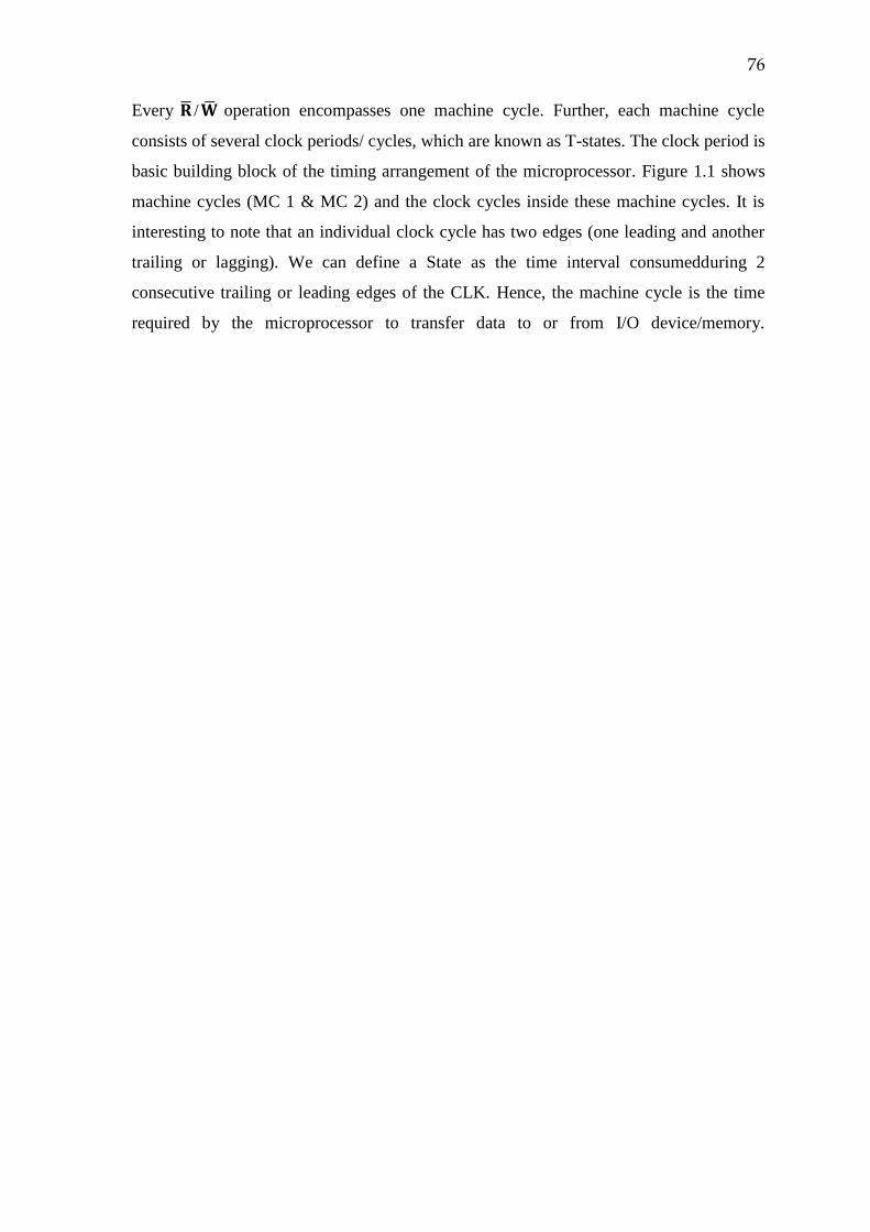
76
Every �� /�� operation encompasses one machine cycle. Further, each machine cycle
consists of several clock periods/ cycles, which are known as T-states. The clock period is
basic building block of the timing arrangement of the microprocessor. Figure 1.1 shows
machine cycles (MC 1 & MC 2) and the clock cycles inside these machine cycles. It is
interesting to note that an individual clock cycle has two edges (one leading and another
trailing or lagging). We can define a State as the time interval consumedduring 2
consecutive trailing or leading edges of the CLK. Hence, the machine cycle is the time
required by the microprocessor to transfer data to or from I/O device/memory.
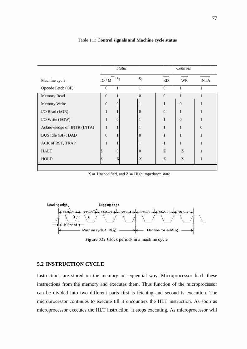
77
Table 1.1: Control signals and Machine cycle status
Status Controls
Machine cycle
S1 S0
IO / M RD WR INTA
Opcode Fetch (OF) 0 1 1 0 1 1
Memory Read 0 1 0 0 1 1
Memory Write 0 0 1 1 0 1
I/O Read (I/OR) 1 1 0 0 1 1
I/O Write (I/OW) 1 0 1 1 0 1
Acknowledge of INTR (INTA) 1 1 1 1 1 0
BUS Idle (BI) : DAD 0 1 0 1 1 1
ACK of RST, TRAP 1 1 1 1 1 1
HALT Z 0 0 Z Z 1
HOLD Z X X Z Z 1
X ⇒ Unspecified, and Z ⇒ High impedance state
5.2 INSTRUCTION CYCLE
Instructions are stored on the memory in sequential way. Microprocessor fetch these
instructions from the memory and executes them. Thus function of the microprocessor
can be divided into two different parts first is fetching and second is execution. The
microprocessor continues to execute till it encounters the HLT instruction. As soon as
microprocessor executes the HLT instruction, it stops executing. As microprocessor will
Figure 0.1: Clock periods in a machine cycle
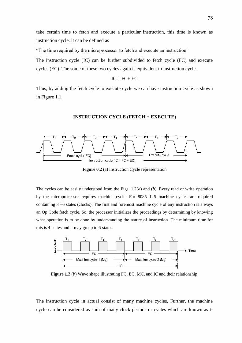
78
take certain time to fetch and execute a particular instruction, this time is known as
instruction cycle. It can be defined as
“The time required by the microprocessor to fetch and execute an instruction”
The instruction cycle (IC) can be further subdivided to fetch cycle (FC) and execute
cycles (EC). The some of these two cycles again is equivalent to instruction cycle.
IC = FC+ EC
Thus, by adding the fetch cycle to execute cycle we can have instruction cycle as shown
in Figure 1.1.
INSTRUCTION CYCLE (FETCH + EXECUTE)
Figure 0.2 (a) Instruction Cycle representation
The cycles can be easily understood from the Figs. 1.2(a) and (b). Every read or write operation
by the microprocessor requires machine cycle. For 8085 1–5 machine cycles are required
containing 3`–6 states (clocks). The first and foremost machine cycle of any instruction is always
an Op Code fetch cycle. So, the processor initializes the proceedings by determining by knowing
what operation is to be done by understanding the nature of instruction. The minimum time for
this is 4-states and it may go up to 6-states.
Figure 1.2 (b) Wave shape illustrating FC, EC, MC, and IC and their relationship
The instruction cycle in actual consist of many machine cycles. Further, the machine
cycle can be considered as sum of many clock periods or cycles which are known as t-
79
states. The first machine cycle (M1) of an instruction is always the opcode fetch cycle.
The processor comes to know about the nature of an instruction in this cycle only. During
M1 cycle the microprocessor load the content of program counter on the address lines and
reads the opcode using read operation. The first three clock cycles means T1, T2 and T3
are utilised for memory read operation while T4 and afterward are used for interpretation
of opcode. The microprocessor decides what type of additional information or data is
required for the execution of instruction and depending upon this decision microprocessor
initiate 1 or 2 machine cycles of memory read or write. The instruction cycle depends
upon the size of instruction and varies within different instructions whereas the opcode
fetch cycle is fixed for normally 4 states.
Let’s take the example of STA instruction, for this instruction first opcode is to be fetched
after fetching opcode address fetch cycle are required to fetch higher order as well as
lower order address. In this case opcode fetch cycle is of one machine cycle only.
Every microprocessor takes certain time for performing specific task which is known as
machine cycle. So, microprocessor requires one machine cycle to access memory or I/O
device. The opcode fetch cycle is fixed to one machine cycle while the execute cycle may
last for one or more than one machine cycle. The duration of the fetch cycle is dependent
on the length of instruction.
5.2.1 INSTRUCTION FETCH (FC):
Microprocessor fetches an instruction form the memory and stores this instruction in an
instruction register. The length of instruction can be one byte, two byte or three byte.
5.2.2 INSTRUCTION EXECUTE (EC)
The microprocessor fetches the instruction in fetch cycle and decodes it in the execution cycle.
These three i.e. an instruction cycle, instruction fetch and execute cycle are related to each other
as shown in the figure 1.2 (a). An instruction cycle is constituted by the five machine cycles
generally named as MC1,MC2,MC3,MC4 and MC5 as indicated in figure 1.2 (c). Microprocessor
requires one machine cycle to access I/O of memory. There can be 4 – 6 states in the fetch cycle
whereas the 3 – 6 states could be there in execute cycle. It may be noted again that the 1st
machine cycle is always the fetch cycle and it provides the detailed identification of the
instruction to be executed.
One machine cycle is required by the fetch portion of an instruction cycle for every bite of
instruction to be fetched. An instruction can be of 1 – 3 byte long, so the instruction fetch is also
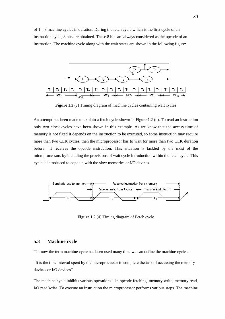
80
of 1 – 3 machine cycles in duration. During the fetch cycle which is the first cycle of an
instruction cycle, 8 bits are obtained. These 8 bits are always considered as the opcode of an
instruction. The machine cycle along with the wait states are shown in the following figure:
Figure 1.2 (c) Timing diagram of machine cycles containing wait cycles
An attempt has been made to explain a fetch cycle shown in Figure 1.2 (d). To read an instruction
only two clock cycles have been shown in this example. As we know that the access time of
memory is not fixed it depends on the instruction to be executed, so some instruction may require
more than two CLK cycles, then the microprocessor has to wait for more than two CLK duration
before it receives the opcode instruction. This situation is tackled by the most of the
microprocessors by including the provisions of wait cycle introduction within the fetch cycle. This
cycle is introduced to cope up with the slow memories or I/O devices.
Figure 1.2 (d) Timing diagram of Fetch cycle
5.3 Machine cycle
Till now the term machine cycle has been used many time we can define the machine cycle as
“It is the time interval spent by the microprocessor to complete the task of accessing the memory
devices or I/O devices”
The machine cycle inhibits various operations like opcode fetching, memory write, memory read,
I/O read/write. To execute an instruction the microprocessor performs various steps. The machine
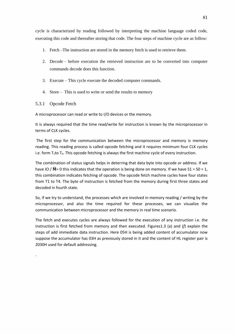
81
cycle is characterized by reading followed by interpreting the machine language coded code,
executing this code and thereafter storing that code. The four steps of machine cycle are as follow:
1. Fetch –The instruction are stored in the memory fetch is used to retrieve them.
2. Decode – before execution the retrieved instruction are to be converted into computer
commands decode does this function.
3. Execute – This cycle execute the decoded computer commands.
4. Store – This is used to write or send the results to memory
5.3.1 Opcode Fetch
A microprocessor can read or write to I/O devices or the memory.
It is always required that the time read/write for instruction is known by the microprocessor in
terms of CLK cycles.
The first step for the communication between the microprocessor and memory is memory
reading. This reading process is called opcode fetching and it requires minimum four CLK cycles
i.e. form T1to T4. This opcode fetching is always the first machine cycle of every instruction.
The combination of status signals helps in deterring that data byte into opcode or address. If we
have IO / ��= 0 this indicates that the operation is being done on memory. If we have S1 = S0 = 1,
this combination indicates fetching of opcode. The opcode fetch machine cycles have four states
from T1 to T4. The byte of instruction is fetched from the memory during first three states and
decoded in fourth state.
So, if we try to understand, the processes which are involved in memory reading / writing by the
microprocessor, and also the time required for these processes, we can visualize the
communication between microprocessor and the memory in real time scenario.
The fetch and executes cycles are always followed for the execution of any instruction i.e. the
instruction is first fetched from memory and then executed. Figures1.3 (a) and (f) explain the
steps of add immediate data instruction. Here 05H is being added content of accumulator now
suppose the accumulator has 03H as previously stored in it and the content of HL register pair is
2030H used for default addressing.
.
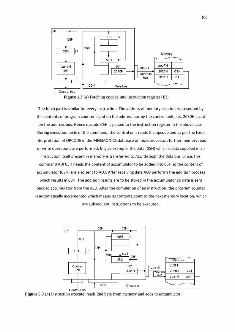
82
Figure 1.3 (a) Fetching opcode into instruction register (IR)
The fetch part is similar for every instruction. The address of memory location represented by
the contents of program counter is put on the address bus by the control unit, i.e., 2030H is put
on the address bus. Hence opcode C6H is passed to the instruction register in the above case.
During execution cycle of the command, the control unit reads the opcode and as per the fixed
interpretation of OPCODE in the MNEMONICS database of microprocessor, further memory read
or write operations are performed. In give example, the data (05H) which is data supplied in an
instruction itself present in memory is transferred to ALU through the data bus. Since, this
command ADI 05H needs the content of accumulator to be added into 05H so the content of
accumulator (03H) are also sent to ALU. After receiving data ALU performs the addition process
which results in 08H. The addition results are to be stored in the accumulator so data is sent
back to accumulator from the ALU. After the completion of an instruction, the program counter
is automatically incremented which means its contents point to the next memory location, which
are subsequent instructions to be executed.
Figure 5.3 (b) Instruction execute: reads 2nd byte from memory and adds to accumulator.
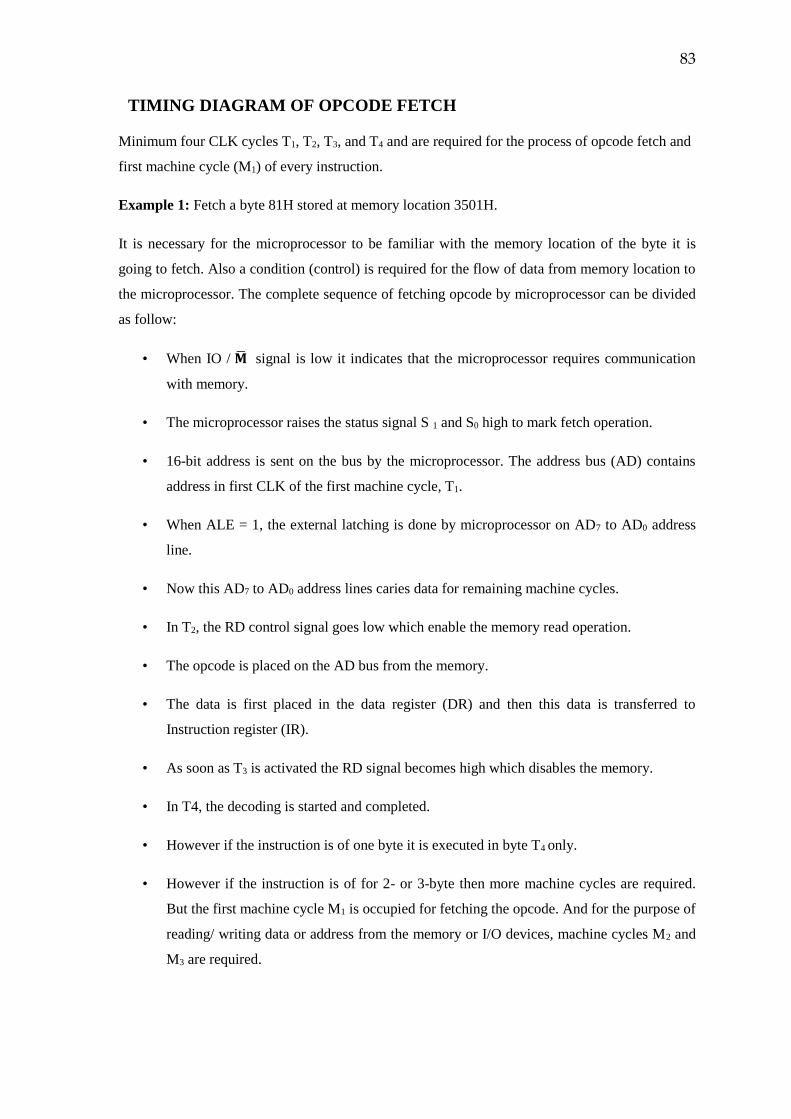
83
TIMING DIAGRAM OF OPCODE FETCH
Minimum four CLK cycles T1, T2, T3, and T4 and are required for the process of opcode fetch and
first machine cycle (M1) of every instruction.
Example 1: Fetch a byte 81H stored at memory location 3501H.
It is necessary for the microprocessor to be familiar with the memory location of the byte it is
going to fetch. Also a condition (control) is required for the flow of data from memory location to
the microprocessor. The complete sequence of fetching opcode by microprocessor can be divided
as follow:
• When IO / �� signal is low it indicates that the microprocessor requires communication
with memory.
• The microprocessor raises the status signal S 1 and S0 high to mark fetch operation.
• 16-bit address is sent on the bus by the microprocessor. The address bus (AD) contains
address in first CLK of the first machine cycle, T1.
• When ALE = 1, the external latching is done by microprocessor on AD7 to AD0 address
line.
• Now this AD7 to AD0 address lines caries data for remaining machine cycles.
• In T2, the RD control signal goes low which enable the memory read operation.
• The opcode is placed on the AD bus from the memory.
• The data is first placed in the data register (DR) and then this data is transferred to
Instruction register (IR).
• As soon as T3 is activated the RD signal becomes high which disables the memory.
• In T4, the decoding is started and completed.
• However if the instruction is of one byte it is executed in byte T4 only.
• However if the instruction is of for 2- or 3-byte then more machine cycles are required.
But the first machine cycle M1 is occupied for fetching the opcode. And for the purpose of
reading/ writing data or address from the memory or I/O devices, machine cycles M2 and
M3 are required.
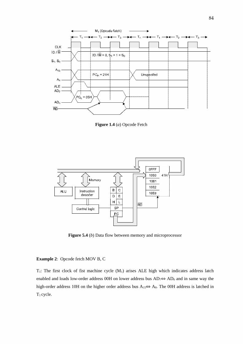
84
Figure 1.4 (a) Opcode Fetch
Figure 5.4 (b) Data flow between memory and microprocessor
Example 2: Opcode fetch MOV B, C
T1: The first clock of fist machine cycle (M1) arises ALE high which indicates address latch
enabled and loads low-order address 00H on lower address bus AD7⇔ AD0 and in same way the
high-order address 10H on the higher order address bus A15⇔ A8. The 00H address is latched in
T1 cycle.
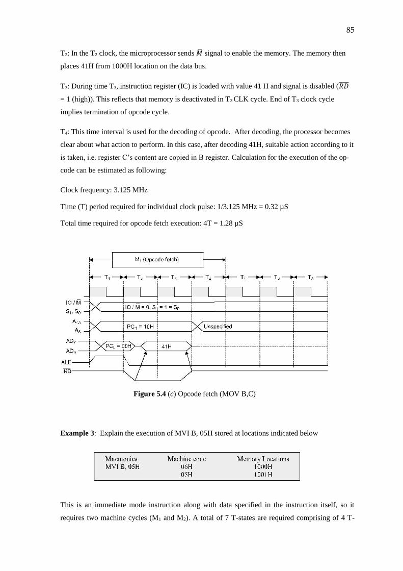
85
T2: In the T2 clock, the microprocessor sends �� signal to enable the memory. The memory then
places 41H from 1000H location on the data bus.
T3: During time T3, instruction register (IC) is loaded with value 41 H and signal is disabled (𝑅𝐷
= 1 (high)). This reflects that memory is deactivated in T3 CLK cycle. End of T3 clock cycle
implies termination of opcode cycle.
T4: This time interval is used for the decoding of opcode. After decoding, the processor becomes
clear about what action to perform. In this case, after decoding 41H, suitable action according to it
is taken, i.e. register C’s content are copied in B register. Calculation for the execution of the op-
code can be estimated as following:
Clock frequency: 3.125 MHz
Time (T) period required for individual clock pulse: 1/3.125 MHz = 0.32 µS
Total time required for opcode fetch execution: 4T = 1.28 µS
Figure 5.4 (c) Opcode fetch (MOV B,C)
Example 3: Explain the execution of MVI B, 05H stored at locations indicated below
This is an immediate mode instruction along with data specified in the instruction itself, so it
requires two machine cycles (M1 and M2). A total of 7 T-states are required comprising of 4 T-
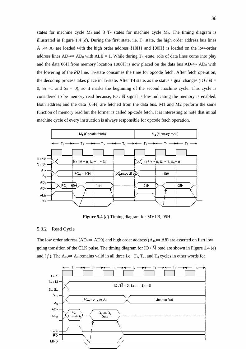
86
states for machine cycle M1 and 3 T- states for machine cycle M2. The timing diagram is
illustrated in Figure 1.4 (d). During the first state, i.e. T1 state, the high order address bus lines
A15⇔ A8 are loaded with the high order address {10H} and {00H} is loaded on the low-order
address lines AD7⇔ AD0 with ALE = 1. While during T2 -state, role of data lines come into play
and the data 06H from memory location 1000H is now placed on the data bus AD7⇔ AD0 with
the lowering of the 𝑅𝐷 line. T3-state consumes the time for opcode fetch. After fetch operation,
the decoding process takes place in T4-state. After T4 state, as the status signal changes (IO / �� =
0, S1 =1 and S0 = 0), so it marks the beginning of the second machine cycle. This cycle is
considered to be memory read because, IO / �� signal is low indicating the memory is enabled.
Both address and the data [05H] are fetched from the data bus. M1 and M2 perform the same
function of memory read but the former is called op-code fetch. It is interesting to note that initial
machine cycle of every instruction is always responsible for opcode fetch operation.
Figure 5.4 (d) Timing diagram for MVI B, 05H
5.3.2 Read Cycle
The low order address (AD7⇔ AD0) and high order address (A15⇔ A8) are asserted on fisrt low
going transition of the CLK pulse. The timing diagram for IO / �� read are shown in Figure 1.4 (e)
and ( f ). The A15⇔ A8 remains valid in all three i.e. T1, T2, and T3 cycles in other words for
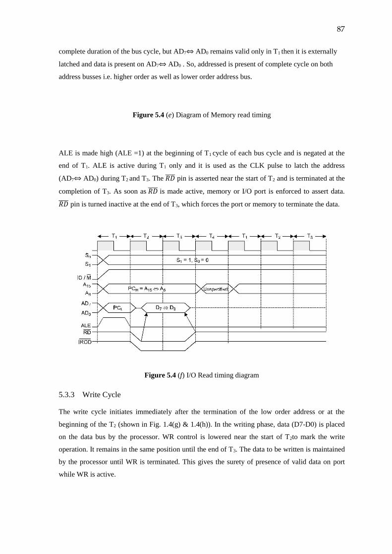
87
complete duration of the bus cycle, but AD7⇔ AD0 remains valid only in T1 then it is externally
latched and data is present on AD7⇔ AD0 . So, addressed is present of complete cycle on both
address busses i.e. higher order as well as lower order address bus.
Figure 5.4 (e) Diagram of Memory read timing
ALE is made high (ALE =1) at the beginning of T1 cycle of each bus cycle and is negated at the
end of T1. ALE is active during T1 only and it is used as the CLK pulse to latch the address
(AD7⇔ AD0) during T2 and T3. The 𝑅𝐷 pin is asserted near the start of T2 and is terminated at the
completion of T3. As soon as 𝑅𝐷 is made active, memory or I/O port is enforced to assert data.
𝑅𝐷 pin is turned inactive at the end of T3, which forces the port or memory to terminate the data.
Figure 5.4 (f) I/O Read timing diagram
5.3.3 Write Cycle
The write cycle initiates immediately after the termination of the low order address or at the
beginning of the T2 (shown in Fig. 1.4(g) & 1.4(h)). In the writing phase, data (D7-D0) is placed
on the data bus by the processor. WR control is lowered near the start of T2to mark the write
operation. It remains in the same position until the end of T3. The data to be written is maintained
by the processor until WR is terminated. This gives the surety of presence of valid data on port
while WR is active.
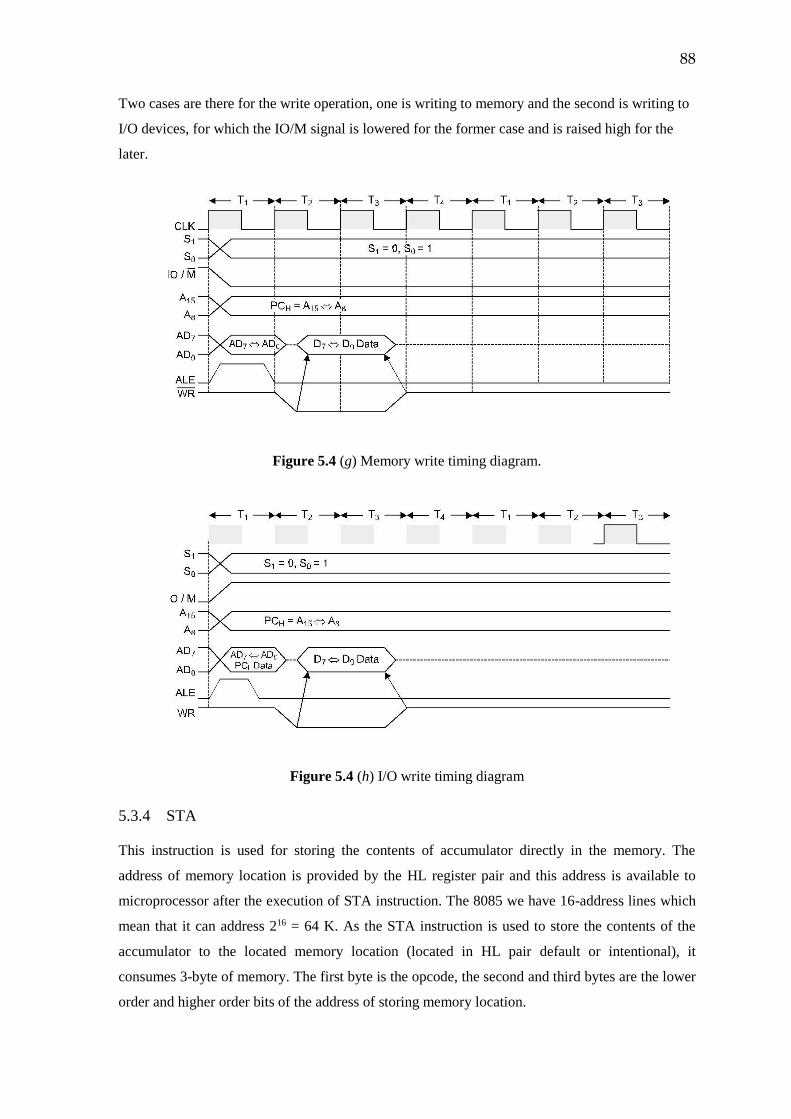
88
Two cases are there for the write operation, one is writing to memory and the second is writing to
I/O devices, for which the IO/M signal is lowered for the former case and is raised high for the
later.
Figure 5.4 (g) Memory write timing diagram.
Figure 5.4 (h) I/O write timing diagram
5.3.4 STA
This instruction is used for storing the contents of accumulator directly in the memory. The
address of memory location is provided by the HL register pair and this address is available to
microprocessor after the execution of STA instruction. The 8085 we have 16-address lines which
mean that it can address 216 = 64 K. As the STA instruction is used to store the contents of the
accumulator to the located memory location (located in HL pair default or intentional), it
consumes 3-byte of memory. The first byte is the opcode, the second and third bytes are the lower
order and higher order bits of the address of storing memory location.
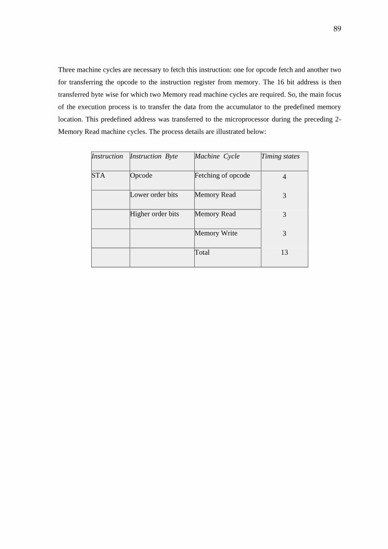
89
Three machine cycles are necessary to fetch this instruction: one for opcode fetch and another two
for transferring the opcode to the instruction register from memory. The 16 bit address is then
transferred byte wise for which two Memory read machine cycles are required. So, the main focus
of the execution process is to transfer the data from the accumulator to the predefined memory
location. This predefined address was transferred to the microprocessor during the preceding 2-
Memory Read machine cycles. The process details are illustrated below:
Instruction Instruction Byte Machine Cycle Timing states
STA Opcode Fetching of opcode 4
3
3
3
13
Lower order bits Memory Read
Higher order bits Memory Read
Memory Write
Total
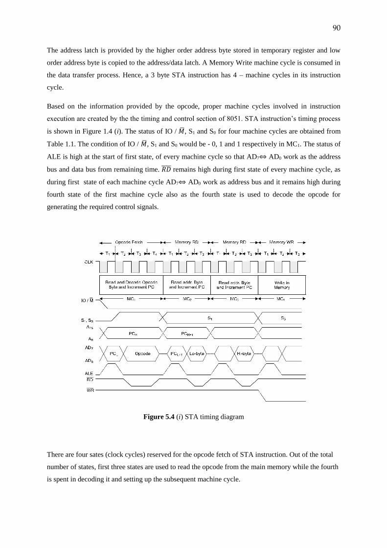
90
The address latch is provided by the higher order address byte stored in temporary register and low
order address byte is copied to the address/data latch. A Memory Write machine cycle is consumed in
the data transfer process. Hence, a 3 byte STA instruction has 4 – machine cycles in its instruction
cycle.
Based on the information provided by the opcode, proper machine cycles involved in instruction
execution are created by the the timing and control section of 8051. STA instruction’s timing process
is shown in Figure 1.4 (i). The status of IO / ��, S1 and S0 for four machine cycles are obtained from
Table 1.1. The condition of IO / ��, S1 and S0 would be - 0, 1 and 1 respectively in MC1. The status of
ALE is high at the start of first state, of every machine cycle so that AD7⇔ AD0 work as the address
bus and data bus from remaining time. 𝑅𝐷 remains high during first state of every machine cycle, as
during first state of each machine cycle AD7⇔ AD0 work as address bus and it remains high during
fourth state of the first machine cycle also as the fourth state is used to decode the opcode for
generating the required control signals.
Figure 5.4 (i) STA timing diagram
There are four sates (clock cycles) reserved for the opcode fetch of STA instruction. Out of the total
number of states, first three states are used to read the opcode from the main memory while the fourth
is spent in decoding it and setting up the subsequent machine cycle.
91
The memory’s action for read or write cycles containing 3 timing states can be explained as:
T1: During this interval, the microprocessor sets up the address and control signals for the process of
memory access.
T2: In this time period, microprocessor checks the status of READY and HOLD control signals.For
READY = 0, the microprocessor enters in the wait state because of indication of a slow memory
device. The wait is done until READY = 1, which may also indicate the DMA request. After this
only, the microprocessor floats the data transfer lines until HOLD = 0.
T3: In this time slot a byte from the data bus is transferred to an internal register pointing to the
function of memory read cycle and similarly vice-versa for memory write cycle i.e. a byte is
transferred from an internal register to the data bus.
The STA instruction in total requires four machine cycles containing 13-states (clock cycles). Using a
typical clock of 3 MHz (= 330 ns), a time of 13*330 ns = 4.29 ms is required for the execution of
STA instruction.
5.4 TERMINAL AND MODEL QUESTIONS
1. You are given with a system operating at frequency 3 MHz, it is required to find out the
execution time of the
a) MOV A,
b) B MOV C,
c) D MOV A,M
d) MVI A,05H
e) MVI B,05H
2. Use appropriate diagram to illustrate the role of timing and control unit in the operation of
microprocessors.
3. Define (a) Clock cycle (b) Machine cycle, (c) Instruction cycle.
4. Explain the memory read instruction using the timing diagram.
5. Illustrate the I/O read write operation with timing diagram.
92
Chapter 6
Introduction to Microcontroller
6.0 Objectives
61 Introduction
62 Microcontroller Architectures
Harvard Architecture
Princeton Architecture
6.3 History of Microcontroller: Next Generation Microcontroller
6.4 Difference between Microprocessor and Microcontroller
6.5 Microcontroller Resources: Features of Microcontroller
6.6. Microcontroller based on CISC & RISC Architectures
Complex instruction Set Computing (CISC)
Reduced Instruction Set Computing( RISC)
6.0 Objectives
This chapter provides the Introduction to Microcontroller . After reading this chapter you will
be able to understand the
Basic microcontroller Architectures
Difference between Microprocessor and Microcontroller
A short history of microcontroller to next Generation Microcontroller
Concept of CISC & RISC Architectures and Various applications
6.1 Introduction
A microcontroller is a programmable logic and integrated circuit which can be programmed
to do a number of tasks. It is possible to control just about anything with the program written
by the user. That’s why Microcontrollers are widely used in embedded applications, in
contrast to the microprocessors used in personal computers or other general purpose
applications. Some of the functions of a microcontroller are-
It is capable to execute a user defined task according to the stored set of instructions for
that defined task.
93
Microcontrollers can read & write data from/to memory by accessing the external memory
chips.
Interface with the I/O devices is also possible with microcontroller.
Basic components of a Microcontroller are-
A CPU to execute programmed code
Memory, both RAM and ROM
Internal timers
An input/output system, in form of i/o pins
Some Microcontrollers have some extra features like-
ADCs and DACs
UART fro serial communication
Internal EEPROM
PWM modules for analogue output
6.2 Microcontroller Architectures
A several year ago America requested to Hardvard and Princeton Universities to invent the
computer architecture which has to be used in the computing also of Naval artillery shell for
the varying of environmental conditions and elevations. There are two basic Computer
architectures:
1. Harvard Architecture
2. Princeton Architecture (Von Neumann Architecture)
6.2.1 Harvard Architecture Princeton
In Harvard architecture the CPU have separate data and instruction memory and busses that
allowing the transfers to be performed simultaneously on both the busses. The design of
Harvard was responsible for the design which is used in separate memory banks for program
storage, for the variable RAM and for the processor stack.
In contrast the Princeton architecture also called von Neumann Architecture by the name of
scientist “Von Neumann”, It was a computer which has the common memory for the storing
the control the program along with data structures and variables. In the Princeton architecture
the CPU can either reading an instruction or reading/writing data from/to the memory. But
both the operation can’t be operate simultaneously because the inductions and data uses the
common bus system.
In the Harvard Architecture the machine have the unique code and data address spaces that is
the instruction address zero is not the as same as data address zero. The instruction address
zero may identify by the 24- bit value. While the data address 0 may indicate the 8-bit byte
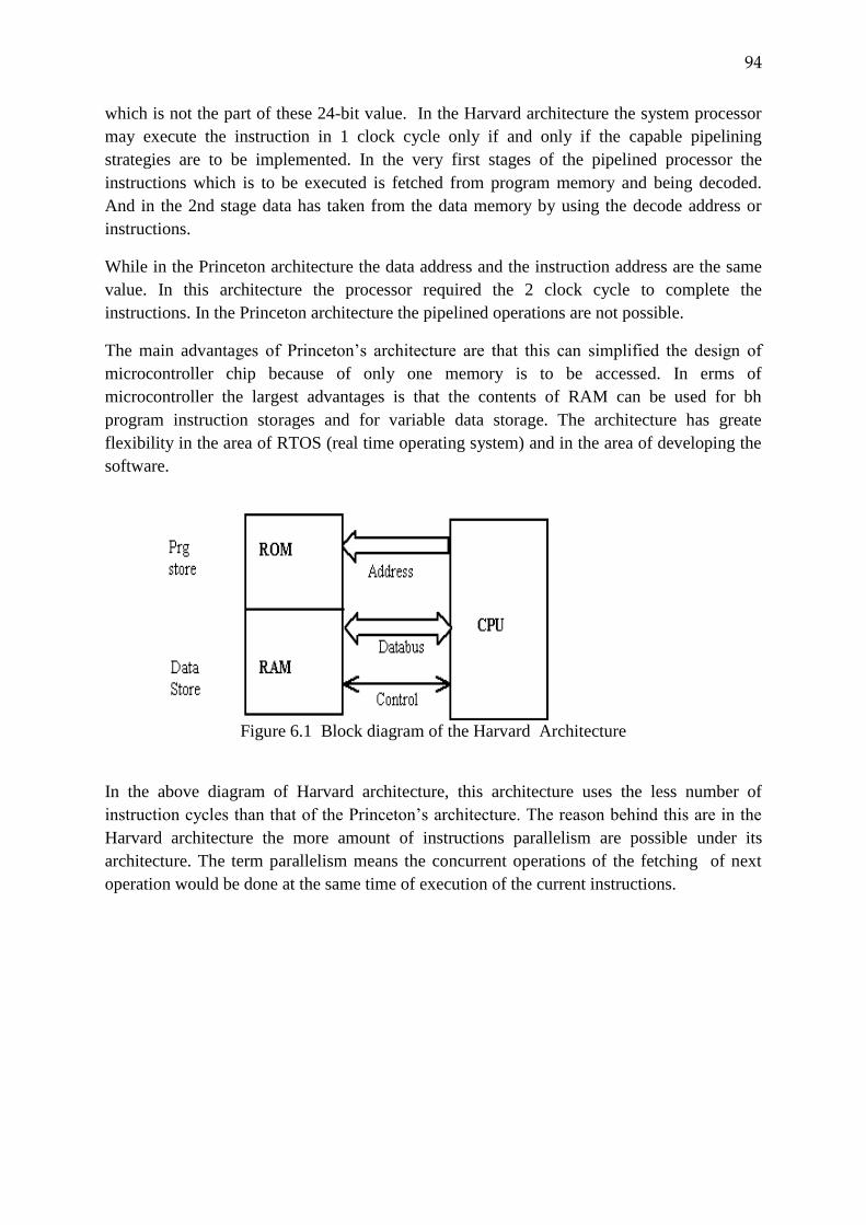
94
which is not the part of these 24-bit value. In the Harvard architecture the system processor
may execute the instruction in 1 clock cycle only if and only if the capable pipelining
strategies are to be implemented. In the very first stages of the pipelined processor the
instructions which is to be executed is fetched from program memory and being decoded.
And in the 2nd stage data has taken from the data memory by using the decode address or
instructions.
While in the Princeton architecture the data address and the instruction address are the same
value. In this architecture the processor required the 2 clock cycle to complete the
instructions. In the Princeton architecture the pipelined operations are not possible.
The main advantages of Princeton’s architecture are that this can simplified the design of
microcontroller chip because of only one memory is to be accessed. In erms of
microcontroller the largest advantages is that the contents of RAM can be used for bh
program instruction storages and for variable data storage. The architecture has greate
flexibility in the area of RTOS (real time operating system) and in the area of developing the
software.
Figure 6.1 Block diagram of the Harvard Architecture
In the above diagram of Harvard architecture, this architecture uses the less number of
instruction cycles than that of the Princeton’s architecture. The reason behind this are in the
Harvard architecture the more amount of instructions parallelism are possible under its
architecture. The term parallelism means the concurrent operations of the fetching of next
operation would be done at the same time of execution of the current instructions.
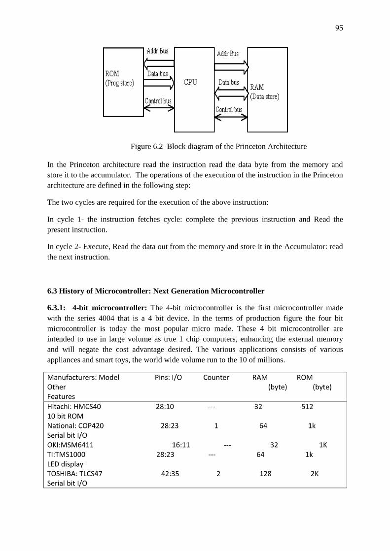
95
Figure 6.2 Block diagram of the Princeton Architecture
In the Princeton architecture read the instruction read the data byte from the memory and
store it to the accumulator. The operations of the execution of the instruction in the Princeton
architecture are defined in the following step:
The two cycles are required for the execution of the above instruction:
In cycle 1- the instruction fetches cycle: complete the previous instruction and Read the
present instruction.
In cycle 2- Execute, Read the data out from the memory and store it in the Accumulator: read
the next instruction.
6.3 History of Microcontroller: Next Generation Microcontroller
6.3.1: 4-bit microcontroller: The 4-bit microcontroller is the first microcontroller made
with the series 4004 that is a 4 bit device. In the terms of production figure the four bit
microcontroller is today the most popular micro made. These 4 bit microcontroller are
intended to use in large volume as true 1 chip computers, enhancing the external memory
and will negate the cost advantage desired. The various applications consists of various
appliances and smart toys, the world wide volume run to the 10 of millions.
Manufacturers: Model Pins: I/O Counter RAM ROM Other (byte) (byte) Features
Hitachi: HMCS40 28:10 --- 32 512 10 bit ROM National: COP420 28:23 1 64 1k Serial bit I/O OKI:MSM6411 16:11 --- 32 1K TI:TMS1000 28:23 --- 64 1k LED display TOSHIBA: TLCS47 42:35 2 128 2K Serial bit I/O
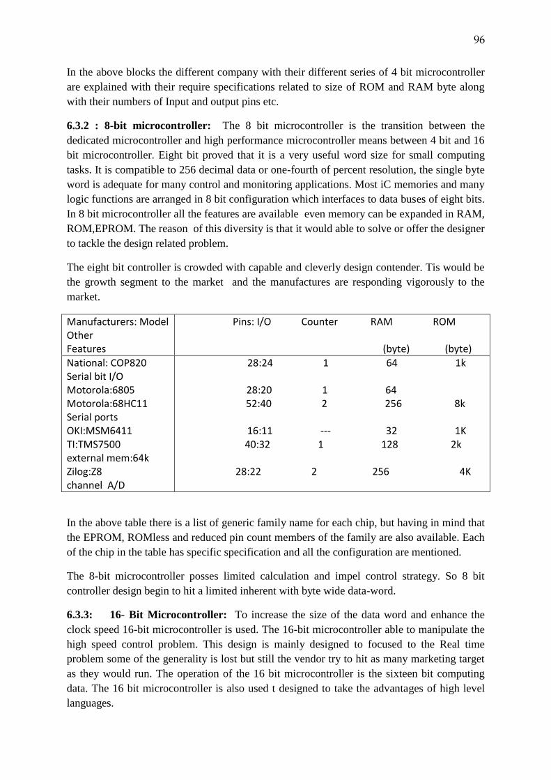
96
In the above blocks the different company with their different series of 4 bit microcontroller
are explained with their require specifications related to size of ROM and RAM byte along
with their numbers of Input and output pins etc.
6.3.2 : 8-bit microcontroller: The 8 bit microcontroller is the transition between the
dedicated microcontroller and high performance microcontroller means between 4 bit and 16
bit microcontroller. Eight bit proved that it is a very useful word size for small computing
tasks. It is compatible to 256 decimal data or one-fourth of percent resolution, the single byte
word is adequate for many control and monitoring applications. Most iC memories and many
logic functions are arranged in 8 bit configuration which interfaces to data buses of eight bits.
In 8 bit microcontroller all the features are available even memory can be expanded in RAM,
ROM,EPROM. The reason of this diversity is that it would able to solve or offer the designer
to tackle the design related problem.
The eight bit controller is crowded with capable and cleverly design contender. Tis would be
the growth segment to the market and the manufactures are responding vigorously to the
market.
Manufacturers: Model Other Features
Pins: I/O Counter RAM ROM
(byte) (byte)
National: COP820 Serial bit I/O Motorola:6805 Motorola:68HC11 Serial ports OKI:MSM6411 TI:TMS7500 external mem:64k Zilog:Z8 channel A/D
28:24 1 64 1k
28:20 1 64 52:40 2 256 8k
16:11 --- 32 1K
40:32 1 128 2k
28:22 2 256 4K
In the above table there is a list of generic family name for each chip, but having in mind that
the EPROM, ROMless and reduced pin count members of the family are also available. Each
of the chip in the table has specific specification and all the configuration are mentioned.
The 8-bit microcontroller posses limited calculation and impel control strategy. So 8 bit
controller design begin to hit a limited inherent with byte wide data-word.
6.3.3: 16- Bit Microcontroller: To increase the size of the data word and enhance the
clock speed 16-bit microcontroller is used. The 16-bit microcontroller able to manipulate the
high speed control problem. This design is mainly designed to focused to the Real time
problem some of the generality is lost but still the vendor try to hit as many marketing target
as they would run. The operation of the 16 bit microcontroller is the sixteen bit computing
data. The 16 bit microcontroller is also used t designed to take the advantages of high level
languages.
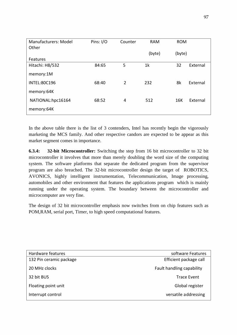
97
Manufacturers: Model Pins: I/O Counter RAM ROM Other (byte) (byte) Features
Hitachi: H8/532 84:65 5 1k 32 External
memory:1M
INTEL:80C196 68:40 2 232 8k External
memory:64K
NATIONAL:hpc16164 68:52 4 512 16K External
memory:64K
In the above table there is the list of 3 contenders, Intel has recently begin the vigorously
marketing the MCS family. And other respective candors are expected to be appear as this
market segment comes in importance.
6.3.4: 32-bit Microcontroller: Switching the step from 16 bit microcontroller to 32 bit
microcontroller it involves that more than merely doubling the word size of the computing
system. The software platforms that separate the dedicated program from the supervisor
program are also breached. The 32-bit microcontroller design the target of ROBOTICS,
AVONICS, highly intelligent instrumentation, Telecommunication, Image processing,
automobiles and other environment that features the applications program which is mainly
running under the operating system. The boundary between the microcontroller and
microcomputer are very fine.
The design of 32 bit microcontroller emphasis now switches from on chip features such as
POM,RAM, serial port, Timer, to high speed computational features.
Hardware features software Features
132 Pin ceramic package Efficient package call
20 MHz clocks Fault handling capability
32 bit BUS Trace Event
Floating point unit Global register
Interrupt control versatile addressing
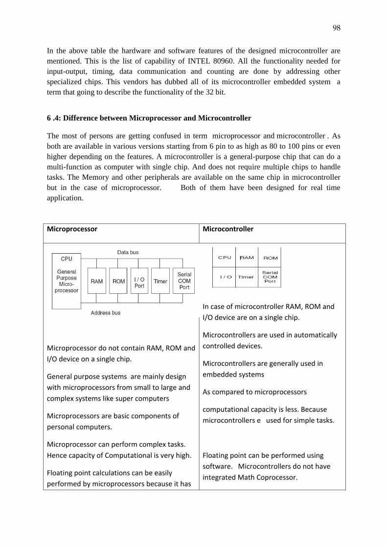
98
In the above table the hardware and software features of the designed microcontroller are
mentioned. This is the list of capability of INTEL 80960. All the functionality needed for
input-output, timing, data communication and counting are done by addressing other
specialized chips. This vendors has dubbed all of its microcontroller embedded system a
term that going to describe the functionality of the 32 bit.
6 .4: Difference between Microprocessor and Microcontroller
The most of persons are getting confused in term microprocessor and microcontroller . As
both are available in various versions starting from 6 pin to as high as 80 to 100 pins or even
higher depending on the features. A microcontroller is a general-purpose chip that can do a
multi-function as computer with single chip. And does not require multiple chips to handle
tasks. The Memory and other peripherals are available on the same chip in microcontroller
but in the case of microprocessor. Both of them have been designed for real time
application.
Microprocessor Microcontroller
Microprocessor do not contain RAM, ROM and
I/O device on a single chip.
General purpose systems are mainly design
with microprocessors from small to large and
complex systems like super computers
Microprocessors are basic components of
personal computers.
Microprocessor can perform complex tasks.
Hence capacity of Computational is very high.
Floating point calculations can be easily
performed by microprocessors because it has
In case of microcontroller RAM, ROM and
I/O device are on a single chip.
Microcontrollers are used in automatically
controlled devices.
Microcontrollers are generally used in
embedded systems
As compared to microprocessors
computational capacity is less. Because
microcontrollers e used for simple tasks.
Floating point can be performed using
software. Microcontrollers do not have
integrated Math Coprocessor.
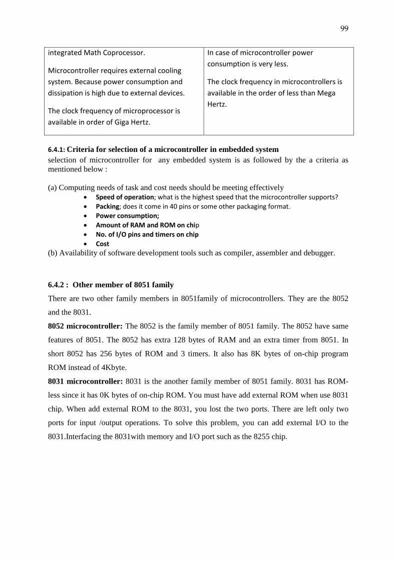
99
integrated Math Coprocessor.
Microcontroller requires external cooling
system. Because power consumption and
dissipation is high due to external devices.
The clock frequency of microprocessor is
available in order of Giga Hertz.
In case of microcontroller power
consumption is very less.
The clock frequency in microcontrollers is
available in the order of less than Mega
Hertz.
6.4.1: Criteria for selection of a microcontroller in embedded system
selection of microcontroller for any embedded system is as followed by the a criteria as
mentioned below :
(a) Computing needs of task and cost needs should be meeting effectively
Speed of operation; what is the highest speed that the microcontroller supports?
Packing; does it come in 40 pins or some other packaging format.
Power consumption;
Amount of RAM and ROM on chip
No. of I/O pins and timers on chip
Cost
(b) Availability of software development tools such as compiler, assembler and debugger.
6.4.2 : Other member of 8051 family
There are two other family members in 8051family of microcontrollers. They are the 8052
and the 8031.
8052 microcontroller: The 8052 is the family member of 8051 family. The 8052 have same
features of 8051. The 8052 has extra 128 bytes of RAM and an extra timer from 8051. In
short 8052 has 256 bytes of ROM and 3 timers. It also has 8K bytes of on-chip program
ROM instead of 4Kbyte.
8031 microcontroller: 8031 is the another family member of 8051 family. 8031 has ROM-
less since it has 0K bytes of on-chip ROM. You must have add external ROM when use 8031
chip. When add external ROM to the 8031, you lost the two ports. There are left only two
ports for input /output operations. To solve this problem, you can add external I/O to the
8031.Interfacing the 8031with memory and I/O port such as the 8255 chip.
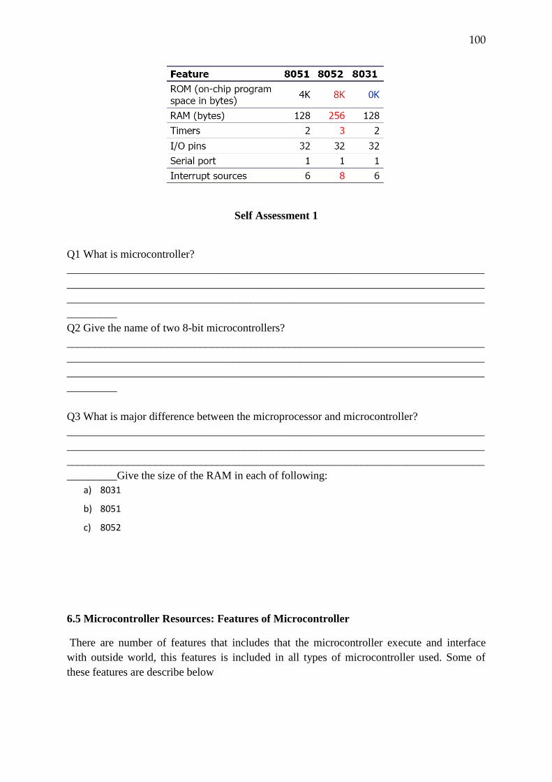
100
Self Assessment 1
Q1 What is microcontroller?
___________________________________________________________________________
___________________________________________________________________________
___________________________________________________________________________
_________
Q2 Give the name of two 8-bit microcontrollers?
___________________________________________________________________________
___________________________________________________________________________
___________________________________________________________________________
_________
Q3 What is major difference between the microprocessor and microcontroller?
___________________________________________________________________________
___________________________________________________________________________
___________________________________________________________________________
_________Give the size of the RAM in each of following:
a) 8031
b) 8051
c) 8052
6.5 Microcontroller Resources: Features of Microcontroller
There are number of features that includes that the microcontroller execute and interface
with outside world, this features is included in all types of microcontroller used. Some of
these features are describe below
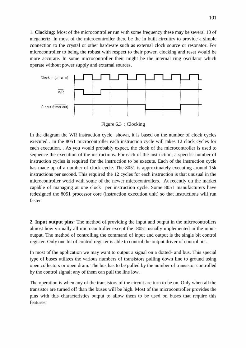
101
1. Clocking: Most of the microcontroller run with some frequency these may be several 10 of
megahertz. In most of the microcontroller there be the in built circuitry to provide a simple
connection to the crystal or other hardware such as external clock source or resonator. For
microcontroller to being the robust with respect to their power, clocking and reset would be
more accurate. In some microcontroller their might be the internal ring oscillator which
operate without power supply and external sources.
Figure 6.3 : Clocking
In the diagram the WR instruction cycle shown, it is based on the number of clock cycles
executed . In the 8051 microcontroller each instruction cycle will takes 12 clock cycles for
each execution. . As you would probably expect, the clock of the microcontroller is used to
sequence the execution of the instructions. For each of the instruction, a specific number of
instruction cycles is required for the instruction to be execute. Each of the instruction cycle
has made up of a number of clock cycle. The 8051 is approximately executing around 15k
instructions per second. This required the 12 cycles for each instruction is that unusual in the
microcontroller world with some of the newer microcontrollers. At recently on the market
capable of managing at one clock per instruction cycle. Some 8051 manufacturers have
redesigned the 8051 processor core (instruction execution unit) so that instructions will run
faster
2. Input output pins: The method of providing the input and output in the microcontrollers
almost how virtually all microcontroller except the 8051 usually implemented in the input-
output. The method of controlling the command of input and output is the single bit control
register. Only one bit of control register is able to control the output driver of control bit .
In most of the application we may want to output a signal on a dotted- and bus. This special
type of buses utilizes the various numbers of transistors pulling down line to ground using
open collectors or open drain. The bus has to be pulled by the number of transistor controlled
by the control signal; any of them can pull the line low.
The operation is when any of the transistors of the circuit are turn to be on. Only when all the
transistor are turned off than the buses will be high. Most of the microcontroller provides the
pins with this characteristics output to allow them to be used on buses that require this
features.
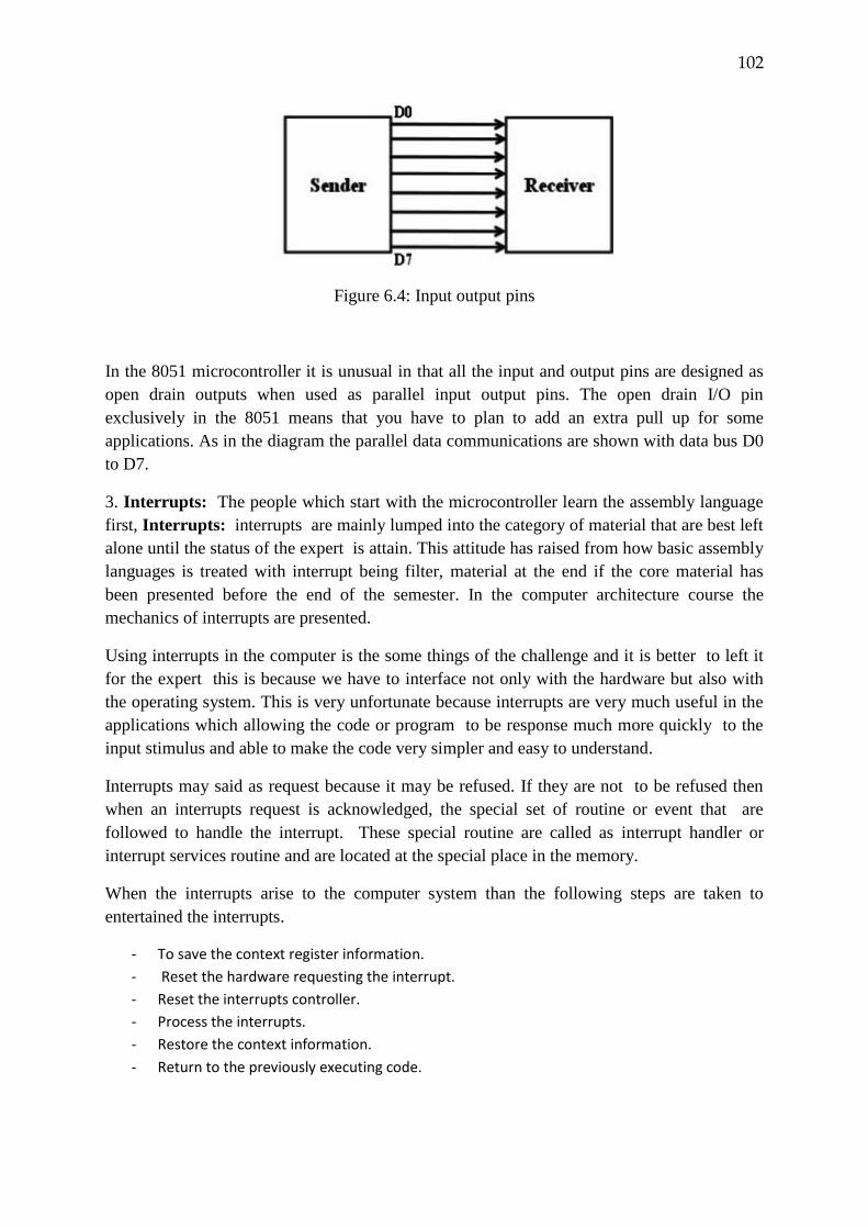
102
Figure 6.4: Input output pins
In the 8051 microcontroller it is unusual in that all the input and output pins are designed as
open drain outputs when used as parallel input output pins. The open drain I/O pin
exclusively in the 8051 means that you have to plan to add an extra pull up for some
applications. As in the diagram the parallel data communications are shown with data bus D0
to D7.
3. Interrupts: The people which start with the microcontroller learn the assembly language
first, Interrupts: interrupts are mainly lumped into the category of material that are best left
alone until the status of the expert is attain. This attitude has raised from how basic assembly
languages is treated with interrupt being filter, material at the end if the core material has
been presented before the end of the semester. In the computer architecture course the
mechanics of interrupts are presented.
Using interrupts in the computer is the some things of the challenge and it is better to left it
for the expert this is because we have to interface not only with the hardware but also with
the operating system. This is very unfortunate because interrupts are very much useful in the
applications which allowing the code or program to be response much more quickly to the
input stimulus and able to make the code very simpler and easy to understand.
Interrupts may said as request because it may be refused. If they are not to be refused then
when an interrupts request is acknowledged, the special set of routine or event that are
followed to handle the interrupt. These special routine are called as interrupt handler or
interrupt services routine and are located at the special place in the memory.
When the interrupts arise to the computer system than the following steps are taken to
entertained the interrupts.
- To save the context register information.
- Reset the hardware requesting the interrupt.
- Reset the interrupts controller.
- Process the interrupts.
- Restore the context information.
- Return to the previously executing code.
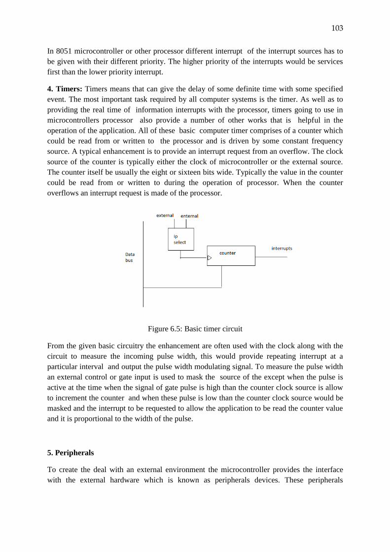
103
In 8051 microcontroller or other processor different interrupt of the interrupt sources has to
be given with their different priority. The higher priority of the interrupts would be services
first than the lower priority interrupt.
4. Timers: Timers means that can give the delay of some definite time with some specified
event. The most important task required by all computer systems is the timer. As well as to
providing the real time of information interrupts with the processor, timers going to use in
microcontrollers processor also provide a number of other works that is helpful in the
operation of the application. All of these basic computer timer comprises of a counter which
could be read from or written to the processor and is driven by some constant frequency
source. A typical enhancement is to provide an interrupt request from an overflow. The clock
source of the counter is typically either the clock of microcontroller or the external source.
The counter itself be usually the eight or sixteen bits wide. Typically the value in the counter
could be read from or written to during the operation of processor. When the counter
overflows an interrupt request is made of the processor.
Figure 6.5: Basic timer circuit
From the given basic circuitry the enhancement are often used with the clock along with the
circuit to measure the incoming pulse width, this would provide repeating interrupt at a
particular interval and output the pulse width modulating signal. To measure the pulse width
an external control or gate input is used to mask the source of the except when the pulse is
active at the time when the signal of gate pulse is high than the counter clock source is allow
to increment the counter and when these pulse is low than the counter clock source would be
masked and the interrupt to be requested to allow the application to be read the counter value
and it is proportional to the width of the pulse.
5. Peripherals
To create the deal with an external environment the microcontroller provides the interface
with the external hardware which is known as peripherals devices. These peripherals
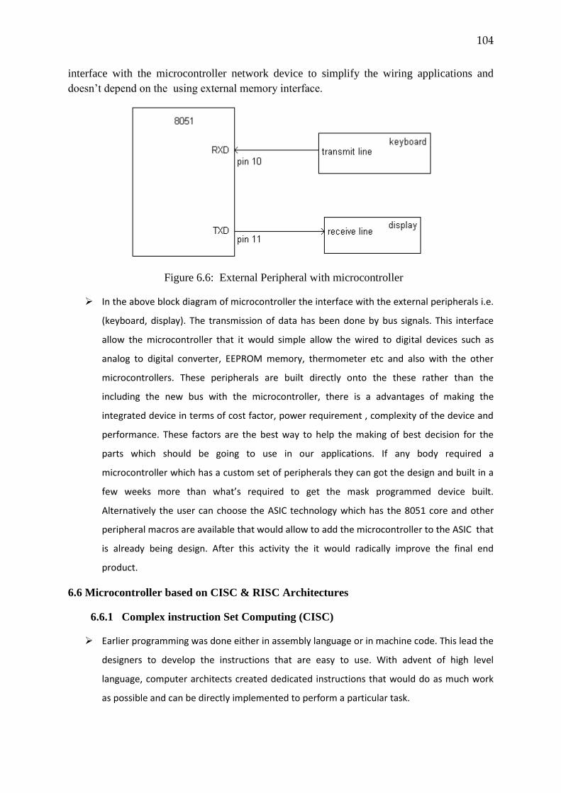
104
interface with the microcontroller network device to simplify the wiring applications and
doesn’t depend on the using external memory interface.
Figure 6.6: External Peripheral with microcontroller
In the above block diagram of microcontroller the interface with the external peripherals i.e.
(keyboard, display). The transmission of data has been done by bus signals. This interface
allow the microcontroller that it would simple allow the wired to digital devices such as
analog to digital converter, EEPROM memory, thermometer etc and also with the other
microcontrollers. These peripherals are built directly onto the these rather than the
including the new bus with the microcontroller, there is a advantages of making the
integrated device in terms of cost factor, power requirement , complexity of the device and
performance. These factors are the best way to help the making of best decision for the
parts which should be going to use in our applications. If any body required a
microcontroller which has a custom set of peripherals they can got the design and built in a
few weeks more than what’s required to get the mask programmed device built.
Alternatively the user can choose the ASIC technology which has the 8051 core and other
peripheral macros are available that would allow to add the microcontroller to the ASIC that
is already being design. After this activity the it would radically improve the final end
product.
6.6 Microcontroller based on CISC & RISC Architectures
6.6.1 Complex instruction Set Computing (CISC)
Earlier programming was done either in assembly language or in machine code. This lead the
designers to develop the instructions that are easy to use. With advent of high level
language, computer architects created dedicated instructions that would do as much work
as possible and can be directly implemented to perform a particular task.
105
Next task was to implement concept of orthogonality that is to provide every addressing
mode for every instruction. This will lead to storage of results and operands directly in
memory instead of register or immediate only.
At that time hardware design was given more importance than compiler design, this became
the reason for implementation of functionality in microcode or hardware rather than
compiler alone. The design philosophy was term as Complex Instruction Set Computer. CISC
chips were the first PC microprocessor as the instructions were built into chips.
Another factor which encouraged this complex architecture was very limited main
memories. This architecture hence proved to be advantageous as it lead to the high density
of information held in computer programs, as well as other features such as variable length
instructions, data loading. These issues were given high priority as compare to ease of
decoding of the instructions.
Other reason was that main memories were slow. With the usage of dense information
packing, frequency with which CPU access memory can be reduced. To overcome these slow
memories, fast cache can be employed but they are of limited size.
CISC Approach
Main motive of designing CISC architecture is that a task can be compiled in very few lines of
assembly. This can be accomplished by implementing a hardware which is capable of
understanding and executing series of operations. For example, if we want to execute a
multiplication operation, then CISC processor comes with a specific instruction(‘MUL’).
When this instruction is executed, two values are loaded into separate registers, operands
are multiplied in execution unit and then product is stored in appropriate registers.
This whole task of multiplication can be compiled in just one instruction
MUL 3:2,2:5
MUL can be called as complex instruction as it directly operates on computer’s memory and
doesn’t require the programmer to call any loading or storing functions.
CISC Architecture
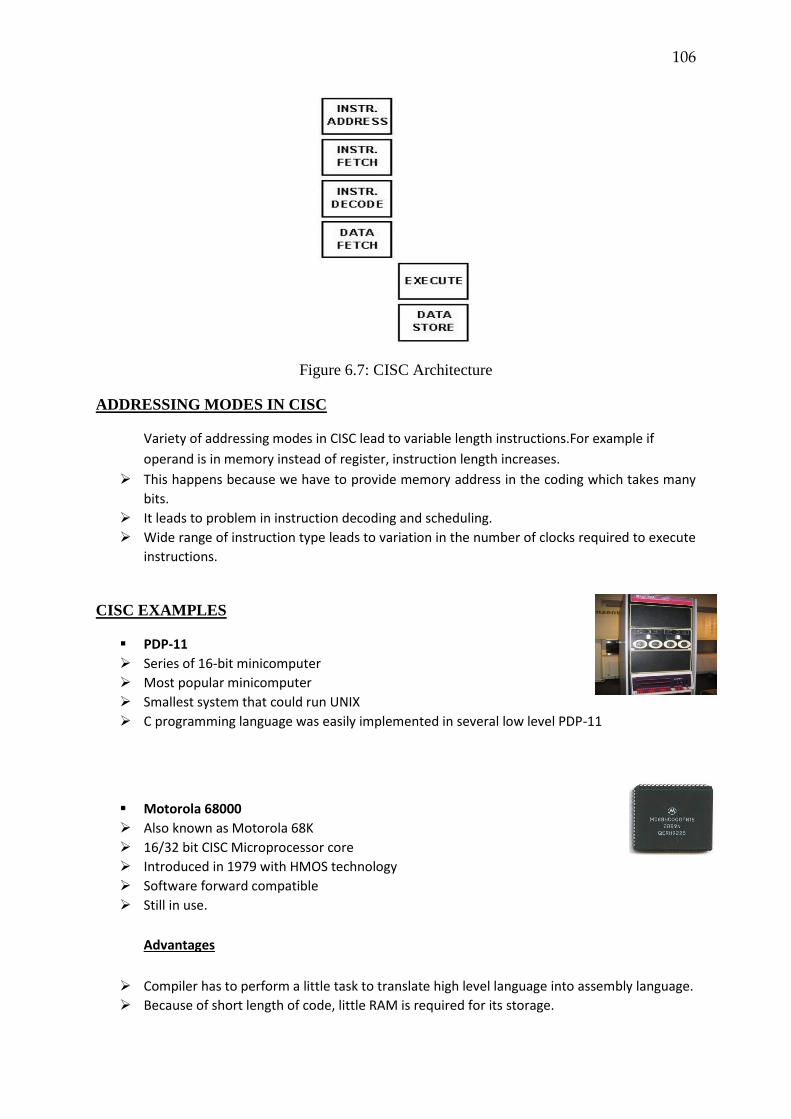
106
Figure 6.7: CISC Architecture
ADDRESSING MODES IN CISC
Variety of addressing modes in CISC lead to variable length instructions.For example if
operand is in memory instead of register, instruction length increases.
This happens because we have to provide memory address in the coding which takes many
bits.
It leads to problem in instruction decoding and scheduling.
Wide range of instruction type leads to variation in the number of clocks required to execute
instructions.
CISC EXAMPLES
PDP-11
Series of 16-bit minicomputer
Most popular minicomputer
Smallest system that could run UNIX
C programming language was easily implemented in several low level PDP-11
Motorola 68000
Also known as Motorola 68K
16/32 bit CISC Microprocessor core
Introduced in 1979 with HMOS technology
Software forward compatible
Still in use.
Advantages
Compiler has to perform a little task to translate high level language into assembly language.
Because of short length of code, little RAM is required for its storage.
107
Disadvantages
Optimisation is difficult
Complex control unit
Hard to exploit complex machine instructions
6.6.2 Reduced Instruction Set Computing( RISC)
RISC stands for reduced instruction set computing. Generally, the term ‘RISC’ is
misunderstood with the concept that number of instructions in RISC is small means it has
small instruction set. But this is not true. We can have any number of instructions until they
are confined within a particular clock period. Their instruction set can be larger than those of
CISC but their complexity is reduced that is why the term reduced instruction set is used.
In RISC, the operation is divided into sub operations. For example, if we want to add two
numbers X and Y then operation will be performed as:
Load ‘X’
Load ‘Y’
Add X and Y
STORE Z
RISC Performance
The thirst for higher performance has always been present in every computer architecture and
model which leads to introduction of new architecture or system organization.
Many methods can be adopted to achieve higher performance such as
i. Technology advances
ii. Better architecture
iii. Better machine organization
iv. Optimization and improvement in compiler technology
By technology, performance is enhanced proportionally to improvement in technology which
is equally available to everyone. It is mainly due to organization of machine and its
architecture where experience and skill of computer design is shown. These goals are fulfilled
by RISC and as a result of RISC architecture we get fewer addressing modes, instructions,
instruction formats and simple circuit for control unit.
RISC architecture is based on concept of pipelining due to which execution time of each
instruction is short and number of cycles are also reduced.
For efficient execution of RISC pipeline most frequently used instructions and addressing
modes are selected.
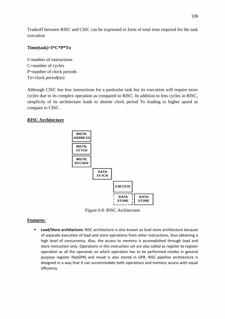
108
Tradeoff between RISC and CISC can be expressed in form of total time required for the task
execution
Time(task)=I*C*P*To
I=number of instructions
C=number of cycles
P=number of clock periods
To=clock period(ns)
Although CISC has less instructions for a particular task but its execution will require more
cycles due to its complex operation as compared to RISC. In addition to less cycles in RISC,
simplicity of its architecture leads to shorter clock period To leading to higher speed as
compare to CISC.
RISC Architecture
Figure 6.8: RISC Architecture
Features:
Load/Store architecture: RISC architecture is also known as load store architecture because
of separate execution of load and store operations from other instructions, thus obtaining a
high level of concurrency. Also, the access to memory is accomplished through load and
store instruction only. Operations in this instruction set are also called as register to register
operation as all the operands on which operation has to be performed resides in general
purpose register file(GPR) and result is also stored in GPR. RISC pipeline architecture is
designed in a way that it can accommodate both operations and memory access with equal
efficiency.
109
Selected set of instructions: Concept of locality is applied in RISC that is small set of
instructions are frequently used leading to efficient instruction level parallelism, hence
efficient pipeline organization. Such pipeline executes three main instruction classes
efficiently.
Load /Store
Arithmetic logic
Branch
Because of its simple pipelined architecture, control part of RISC is implemented in hardware
while CISC heavily depends on microcoding.
Fixed format of instruction: One of the important feature of RISC is its fixed and
predetermined format and instructions which results in decoding of instruction in one cycle
and simplify the control hardware. The size of instruction is fixed to 32 bits, but there can be
two sizes of instruction 32 bit and 16 bit.16-bit size instruction is used in IBM ROMP
processor. Fixed size instruction results in efficient execution of pipelined architecture. This
property of decoding of instruction in one cycle is also helpful in execution of branch
instruction where its outcome can be determined in one cycle and at the same time,
instruction address in new target will be issued.
Simple addressing modes: One of the essential requirement of pipeline is simple addressing
mode as it leads to address calculation in predetermined number of pipeline cycles. In real
programmes, address computation requires only three simple addressing modes.
I. Immediate
II. Base + displacement
III. Base + Index
These addressing modes cover 80% of all addressing modes implemented in as process.
Separate instruction and data Caches: Generally, operands are found in first level of
memory hierarchy, that is in general purpose register file(GPR). This is register to register
operation feature. Access to data from GPR is fast. If operands are not present in GPR, it
should not take long time to fetch data. This require access to a fast memory which is next
to CPU that is Cache. RISC machine requires only one cache cycle for its efficient working, if
it takes two or more cycles, the performance is degraded to maintain 1- cycle cache
bandwidth instruction and data access should not collide. This feature of separation of data
caches and instruction is present in Harvard architecture which is a must feature for RISC.
Pipelining: One of the most important features of RISC architecture is pipelining.
Concept of pipelining
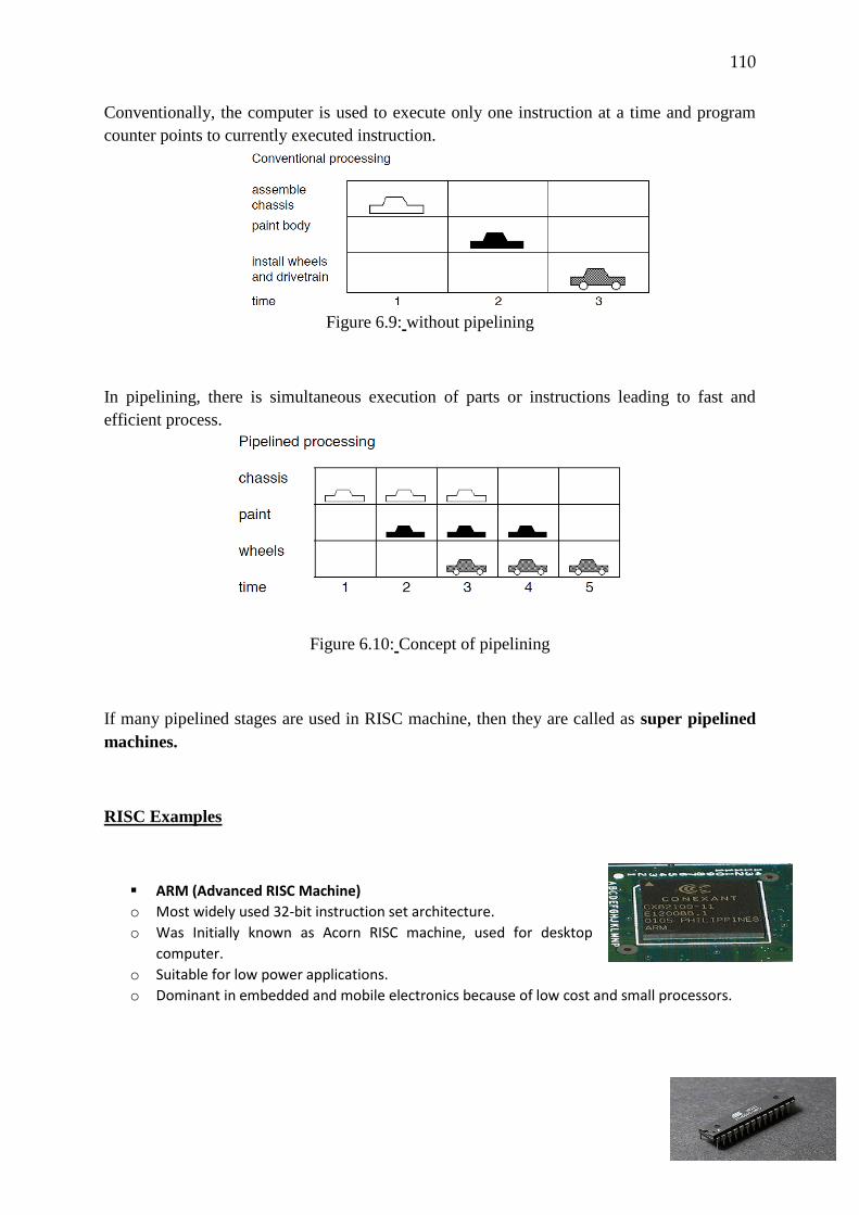
110
Conventionally, the computer is used to execute only one instruction at a time and program
counter points to currently executed instruction.
Figure 6.9: without pipelining
In pipelining, there is simultaneous execution of parts or instructions leading to fast and
efficient process.
Figure 6.10: Concept of pipelining
If many pipelined stages are used in RISC machine, then they are called as super pipelined
machines.
RISC Examples
ARM (Advanced RISC Machine)
o Most widely used 32-bit instruction set architecture.
o Was Initially known as Acorn RISC machine, used for desktop
computer.
o Suitable for low power applications.
o Dominant in embedded and mobile electronics because of low cost and small processors.
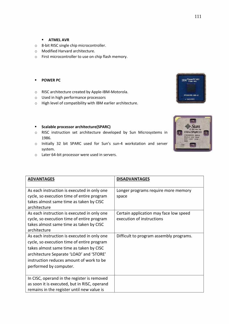
111
ATMEL AVR
o 8-bit RISC single chip microcontroller.
o Modified Harvard architecture.
o First microcontroller to use on chip flash memory.
POWER PC
o RISC architecture created by Apple-IBM-Motorola.
o Used in high performance processors
o High level of compatibility with IBM earlier architecture.
Scalable processor architecture(SPARC)
o RISC instruction set architecture developed by Sun Microsystems in
1986.
o Initially 32 bit SPARC used for Sun’s sun-4 workstation and server
system.
o Later 64-bit processor were used in servers.
ADVANTAGES
DISADVANTAGES
As each instruction is executed in only one cycle, so execution time of entire program takes almost same time as taken by CISC architecture
Longer programs require more memory space
As each instruction is executed in only one cycle, so execution time of entire program takes almost same time as taken by CISC architecture
Certain application may face low speed execution of instructions
As each instruction is executed in only one
cycle, so execution time of entire program
takes almost same time as taken by CISC
architecture Separate ‘LOAD’ and ‘STORE’
instruction reduces amount of work to be
performed by computer.
Difficult to program assembly programs.
In CISC, operand in the register is removed as soon it is executed, but in RISC, operand remains in the register until new value is
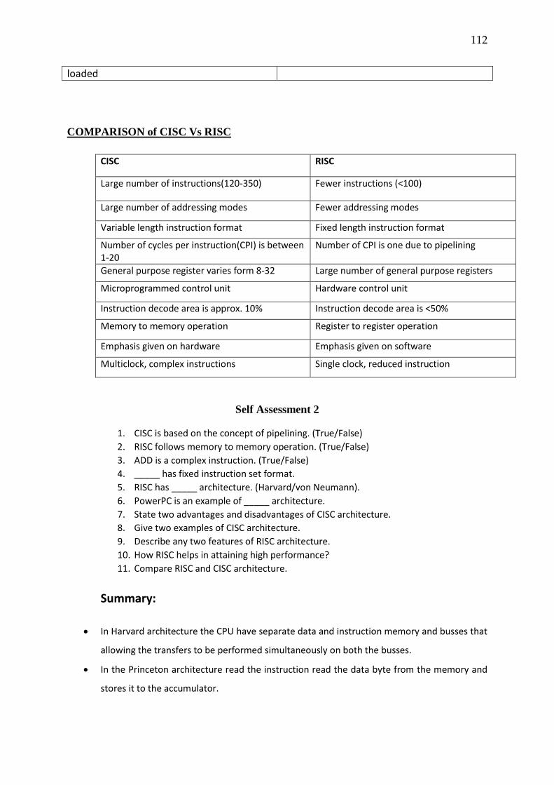
112
loaded
COMPARISON of CISC Vs RISC
CISC RISC
Large number of instructions(120-350) Fewer instructions (<100)
Large number of addressing modes Fewer addressing modes
Variable length instruction format Fixed length instruction format
Number of cycles per instruction(CPI) is between 1-20
Number of CPI is one due to pipelining
General purpose register varies form 8-32 Large number of general purpose registers
Microprogrammed control unit Hardware control unit
Instruction decode area is approx. 10% Instruction decode area is <50%
Memory to memory operation Register to register operation
Emphasis given on hardware Emphasis given on software
Multiclock, complex instructions Single clock, reduced instruction
Self Assessment 2
1. CISC is based on the concept of pipelining. (True/False)
2. RISC follows memory to memory operation. (True/False)
3. ADD is a complex instruction. (True/False)
4. _____ has fixed instruction set format.
5. RISC has _____ architecture. (Harvard/von Neumann).
6. PowerPC is an example of _____ architecture.
7. State two advantages and disadvantages of CISC architecture.
8. Give two examples of CISC architecture.
9. Describe any two features of RISC architecture.
10. How RISC helps in attaining high performance?
11. Compare RISC and CISC architecture.
Summary:
In Harvard architecture the CPU have separate data and instruction memory and busses that
allowing the transfers to be performed simultaneously on both the busses.
In the Princeton architecture read the instruction read the data byte from the memory and
stores it to the accumulator.
113
Computing needs of task and cost needs should be meeting effectively are speed of operation; Packing; Power consumption; Amount of RAM and ROM on chip, No. of I/O pins and timers on chip Cost
The main Microcontroller Resources are. Clocking, Input output pins, Interrupts, Timers, and
Peripherals.
Complex instruction Set Computing (CISC):A processor where each instruction can perform
several low-level operation such as memory access, arithmetic operations or address
calculations.
Reduced Instruction Set Computing( RISC): RISC (reduced instruction set computer) is
a microprocessor that is designed to perform a smaller number of types of
computer instructions so that it can operate at a higher speed (perform more millions of
instructions per second, or MIPS)
Answers to Check Your Progress/Suggested Answers to SAQ
Self Assessment 1
Solution Q1 A microcontroller is a programmable logic and integrated circuit which can be
programmed to do a number of tasks. It is possible to control just about anything with the
program written by the user. That’s why Microcontrollers are widely used in embedded
applications, in contrast to the microprocessors used in personal computers or other general
purpose applications. Some of the functions of a microcontroller are-
It is capable to execute a user defined task according to the stored set of instructions
for that defined task.
Microcontrollers can read & write data from/to memory by accessing the external memory
chips.
Interface with the I/O devices is also possible with microcontroller.
Basic components of a Microcontroller are-
A CPU to execute programmed code
Memory, both RAM and ROM
Internal timers
An input/output system, in form of i/o pins
Solution Q2
There are two other family members in 8051family of microcontrollers. They are the 8052
and the 8031.
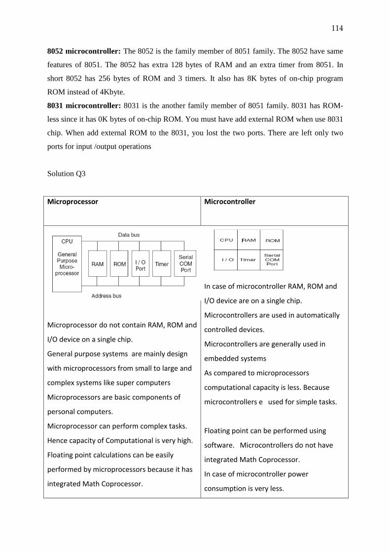
114
8052 microcontroller: The 8052 is the family member of 8051 family. The 8052 have same
features of 8051. The 8052 has extra 128 bytes of RAM and an extra timer from 8051. In
short 8052 has 256 bytes of ROM and 3 timers. It also has 8K bytes of on-chip program
ROM instead of 4Kbyte.
8031 microcontroller: 8031 is the another family member of 8051 family. 8031 has ROM-
less since it has 0K bytes of on-chip ROM. You must have add external ROM when use 8031
chip. When add external ROM to the 8031, you lost the two ports. There are left only two
ports for input /output operations
Solution Q3
Microprocessor Microcontroller
Microprocessor do not contain RAM, ROM and
I/O device on a single chip.
General purpose systems are mainly design
with microprocessors from small to large and
complex systems like super computers
Microprocessors are basic components of
personal computers.
Microprocessor can perform complex tasks.
Hence capacity of Computational is very high.
Floating point calculations can be easily
performed by microprocessors because it has
integrated Math Coprocessor.
In case of microcontroller RAM, ROM and
I/O device are on a single chip.
Microcontrollers are used in automatically
controlled devices.
Microcontrollers are generally used in
embedded systems
As compared to microprocessors
computational capacity is less. Because
microcontrollers e used for simple tasks.
Floating point can be performed using
software. Microcontrollers do not have
integrated Math Coprocessor.
In case of microcontroller power
consumption is very less.
115
Microcontroller requires external cooling
system. Because power consumption and
dissipation is high due to external devices.
The clock frequency of microprocessor is
available in order of Giga Hertz.
The clock frequency in microcontrollers is
available in the order of less than Mega
Hertz.
Self Assessment 2
Q7 Advantages of CISC
Compiler has to perform a little task to translate high level language into assembly language.
Because of short length of code, little RAM is required for its storage.
Disadvantages of CSIC
Optimisation is difficult
Complex control unit
Hard to exploit complex machine instructions
Q8 CISC EXAMPLES
PDP-11
Series of 16-bit minicomputer
Most popular minicomputer
Smallest system that could run UNIX
C programming language was easily implemented in several low level PDP-11
Motorola 68000
Also known as Motorola 68K
16/32 bit CISC Microprocessor core
Introduced in 1979 with HMOS technology
Software forward compatible
Q9 Features of RISC architecture
o Load/Store architecture:
o Selected set of instructions:
o Fixed format of instruction:
o Simple addressing modes.
o Separate instruction and data Caches
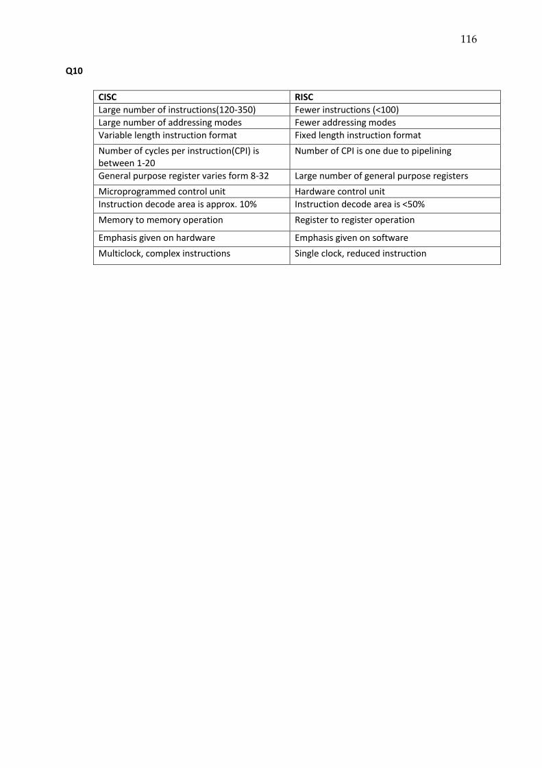
116
Q10
CISC RISC
Large number of instructions(120-350) Fewer instructions (<100)
Large number of addressing modes Fewer addressing modes
Variable length instruction format Fixed length instruction format
Number of cycles per instruction(CPI) is between 1-20
Number of CPI is one due to pipelining
General purpose register varies form 8-32 Large number of general purpose registers
Microprogrammed control unit Hardware control unit
Instruction decode area is approx. 10% Instruction decode area is <50%
Memory to memory operation Register to register operation
Emphasis given on hardware Emphasis given on software
Multiclock, complex instructions Single clock, reduced instruction
117
Chapter 7
Introduction to Microcontroller 8051
7.1 Introduction
7.1.1 Difference between Microprocessor and Microcontroller
7.2 Pin Diagrams of 8051
7.3 Architecture of Microcontroller 8051
7.3.1. Internal RAM and ROM
7.3.2 Input Output Ports of 8051 microcontroller
7.3.3 Timers and Counters in 8051 microcontroller:
7.4 Block Diagram of Architecture Of 8051
7.4.1 Accumulator and B-Registers
7.4.2 Program Counter (PC) and Data Pointer
7.4.3 Data Pointer(DPTR)
7.4.4 ROM Memory Map in 8051
7.4.5 8051 Flag Bits and the PSW Registers
7.4.6 The Stack and the Stack Pointer:
7.0 Objectives
This chapter provides the detail of 8051 Microcontroller. After reading this chapter you will
be able to understand the
Basic microcontroller 8051 Architectures
Difference between Microprocessor and Microcontroller
Pin description of the 8051
Concept of stack pointer, flags , and RAM & ROM mapping
7.1 Introduction
A microcontroller is a programmable logic and integrated circuit which can be programmed
to do a number of tasks. It is possible to control just about anything with the program written
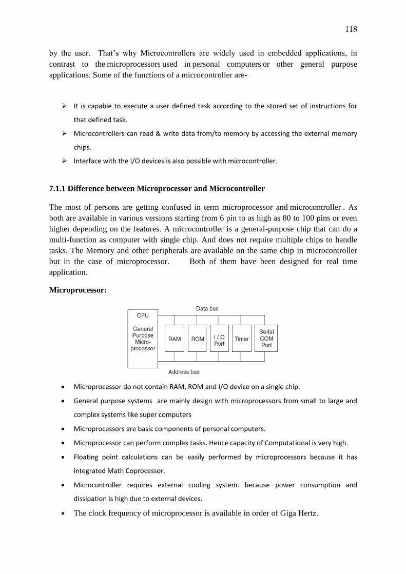
118
by the user. That’s why Microcontrollers are widely used in embedded applications, in
contrast to the microprocessors used in personal computers or other general purpose
applications. Some of the functions of a microcontroller are-
It is capable to execute a user defined task according to the stored set of instructions for
that defined task.
Microcontrollers can read & write data from/to memory by accessing the external memory
chips.
Interface with the I/O devices is also possible with microcontroller.
7.1.1 Difference between Microprocessor and Microcontroller
The most of persons are getting confused in term microprocessor and microcontroller . As
both are available in various versions starting from 6 pin to as high as 80 to 100 pins or even
higher depending on the features. A microcontroller is a general-purpose chip that can do a
multi-function as computer with single chip. And does not require multiple chips to handle
tasks. The Memory and other peripherals are available on the same chip in microcontroller
but in the case of microprocessor. Both of them have been designed for real time
application.
Microprocessor:
Microprocessor do not contain RAM, ROM and I/O device on a single chip.
General purpose systems are mainly design with microprocessors from small to large and
complex systems like super computers
Microprocessors are basic components of personal computers.
Microprocessor can perform complex tasks. Hence capacity of Computational is very high.
Floating point calculations can be easily performed by microprocessors because it has
integrated Math Coprocessor.
Microcontroller requires external cooling system. because power consumption and
dissipation is high due to external devices.
The clock frequency of microprocessor is available in order of Giga Hertz.
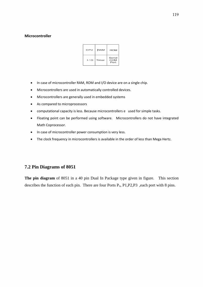
119
Microcontroller
In case of microcontroller RAM, ROM and I/O device are on a single chip.
Microcontrollers are used in automatically controlled devices.
Microcontrollers are generally used in embedded systems
As compared to microprocessors
computational capacity is less. Because microcontrollers e used for simple tasks.
Floating point can be performed using software. Microcontrollers do not have integrated
Math Coprocessor.
In case of microcontroller power consumption is very less.
The clock frequency in microcontrollers is available in the order of less than Mega Hertz.
7.2 Pin Diagrams of 8051
The pin diagram of 8051 in a 40 pin Dual In Package type given in figure. This section
describes the function of each pin. There are four Ports Po, P1,P2,P3 ,each port with 8 pins.
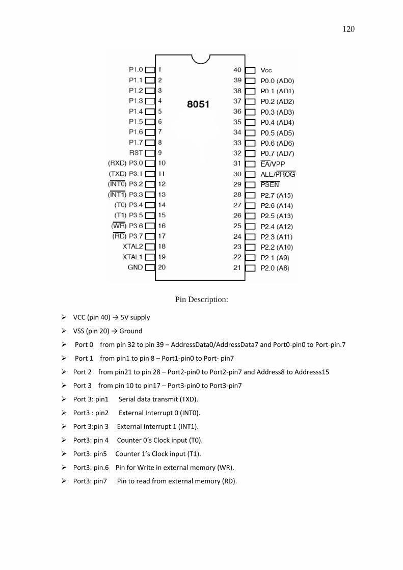
120
Pin Description:
VCC (pin 40) → 5V supply
VSS (pin 20) → Ground
Port 0 from pin 32 to pin 39 – AddressData0/AddressData7 and Port0-pin0 to Port-pin.7
Port 1 from pin1 to pin 8 – Port1-pin0 to Port- pin7
Port 2 from pin21 to pin 28 – Port2-pin0 to Port2-pin7 and Address8 to Addresss15
Port 3 from pin 10 to pin17 – Port3-pin0 to Port3-pin7
Port 3: pin1 Serial data transmit (TXD).
Port3 : pin2 External Interrupt 0 (INT0).
Port 3:pin 3 External Interrupt 1 (INT1).
Port3: pin 4 Counter 0‘s Clock input (T0).
Port3: pin5 Counter 1’s Clock input (T1).
Port3: pin.6 Pin for Write in external memory (WR).
Port3: pin7 Pin to read from external memory (RD).
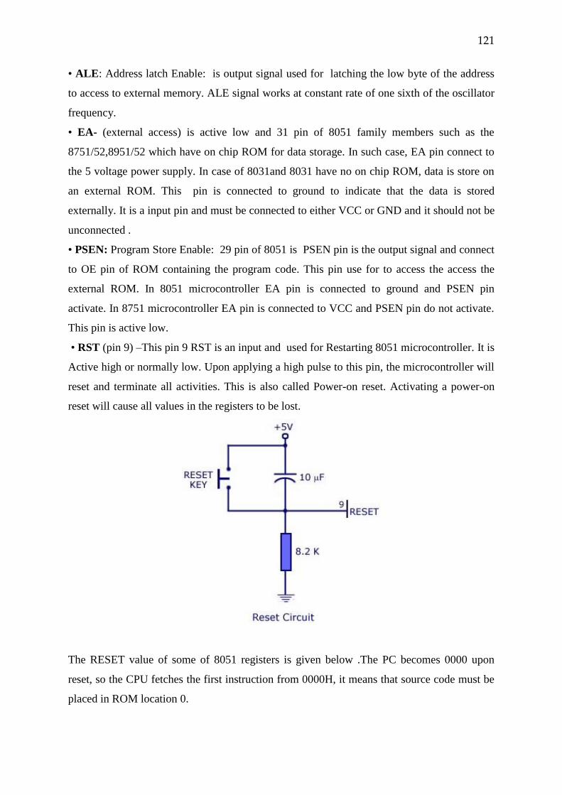
121
• ALE: Address latch Enable: is output signal used for latching the low byte of the address
to access to external memory. ALE signal works at constant rate of one sixth of the oscillator
frequency.
• EA- (external access) is active low and 31 pin of 8051 family members such as the
8751/52,8951/52 which have on chip ROM for data storage. In such case, EA pin connect to
the 5 voltage power supply. In case of 8031and 8031 have no on chip ROM, data is store on
an external ROM. This pin is connected to ground to indicate that the data is stored
externally. It is a input pin and must be connected to either VCC or GND and it should not be
unconnected .
• PSEN: Program Store Enable: 29 pin of 8051 is PSEN pin is the output signal and connect
to OE pin of ROM containing the program code. This pin use for to access the access the
external ROM. In 8051 microcontroller EA pin is connected to ground and PSEN pin
activate. In 8751 microcontroller EA pin is connected to VCC and PSEN pin do not activate.
This pin is active low.
• RST (pin 9) –This pin 9 RST is an input and used for Restarting 8051 microcontroller. It is
Active high or normally low. Upon applying a high pulse to this pin, the microcontroller will
reset and terminate all activities. This is also called Power-on reset. Activating a power-on
reset will cause all values in the registers to be lost.
The RESET value of some of 8051 registers is given below .The PC becomes 0000 upon
reset, so the CPU fetches the first instruction from 0000H, it means that source code must be
placed in ROM location 0.
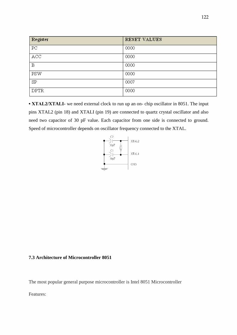
122
• XTAL2/XTALI- we need external clock to run up an on- chip oscillator in 8051. The input
pins XTAL2 (pin 18) and XTALI (pin 19) are connected to quartz crystal oscillator and also
need two capacitor of 30 pF value. Each capacitor from one side is connected to ground.
Speed of microcontroller depends on oscillator frequency connected to the XTAL.
7.3 Architecture of Microcontroller 8051
The most popular general purpose microcontroller is Intel 8051 Microcontroller
Features:
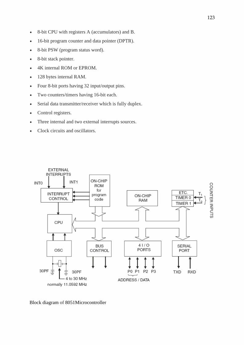
123
8-bit CPU with registers A (accumulators) and B.
16-bit program counter and data pointer (DPTR).
8-bit PSW (program status word).
8-bit stack pointer.
4K internal ROM or EPROM.
128 bytes internal RAM.
Four 8-bit ports having 32 input/output pins.
Two counters/timers having 16-bit each.
Serial data transmitter/receiver which is fully duplex.
Control registers.
Three internal and two external interrupts sources.
Clock circuits and oscillators.
Block diagram of 8051Microcontroller
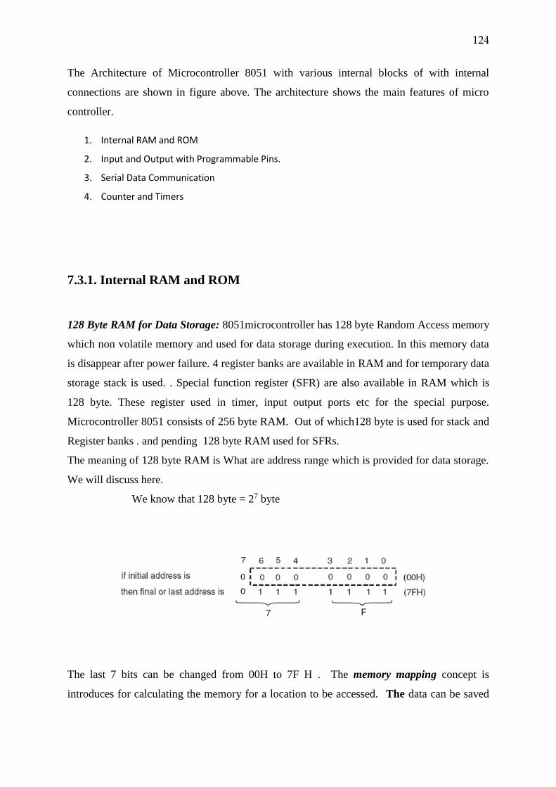
124
The Architecture of Microcontroller 8051 with various internal blocks of with internal
connections are shown in figure above. The architecture shows the main features of micro
controller.
1. Internal RAM and ROM
2. Input and Output with Programmable Pins.
3. Serial Data Communication
4. Counter and Timers
7.3.1. Internal RAM and ROM
128 Byte RAM for Data Storage: 8051microcontroller has 128 byte Random Access memory
which non volatile memory and used for data storage during execution. In this memory data
is disappear after power failure. 4 register banks are available in RAM and for temporary data
storage stack is used. . Special function register (SFR) are also available in RAM which is
128 byte. These register used in timer, input output ports etc for the special purpose.
Microcontroller 8051 consists of 256 byte RAM. Out of which128 byte is used for stack and
Register banks . and pending 128 byte RAM used for SFRs.
The meaning of 128 byte RAM is What are address range which is provided for data storage.
We will discuss here.
We know that 128 byte = 27 byte
The last 7 bits can be changed from 00H to 7F H . The memory mapping concept is
introduces for calculating the memory for a location to be accessed. The data can be saved
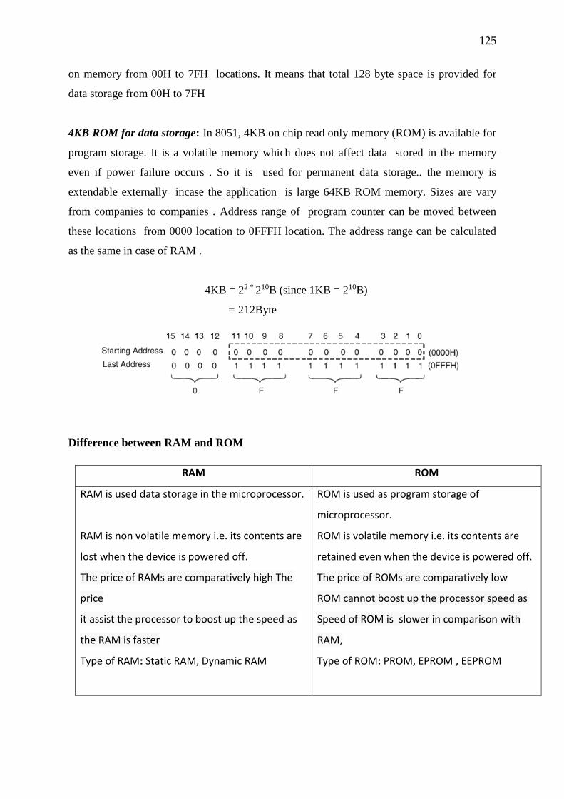
125
on memory from 00H to 7FH locations. It means that total 128 byte space is provided for
data storage from 00H to 7FH
4KB ROM for data storage: In 8051, 4KB on chip read only memory (ROM) is available for
program storage. It is a volatile memory which does not affect data stored in the memory
even if power failure occurs . So it is used for permanent data storage.. the memory is
extendable externally incase the application is large 64KB ROM memory. Sizes are vary
from companies to companies . Address range of program counter can be moved between
these locations from 0000 location to 0FFFH location. The address range can be calculated
as the same in case of RAM .
4KB = 22 * 210B (since 1KB = 210B)
= 212Byte
Difference between RAM and ROM
RAM ROM
RAM is used data storage in the microprocessor.
RAM is non volatile memory i.e. its contents are
lost when the device is powered off.
The price of RAMs are comparatively high The
price
it assist the processor to boost up the speed as
the RAM is faster
Type of RAM: Static RAM, Dynamic RAM
ROM is used as program storage of
microprocessor.
ROM is volatile memory i.e. its contents are
retained even when the device is powered off.
The price of ROMs are comparatively low
ROM cannot boost up the processor speed as
Speed of ROM is slower in comparison with
RAM,
Type of ROM: PROM, EPROM , EEPROM
126
9.3.2 Input Output Ports of 8051 microcontroller
In 8051 there four 8-bit input/output ports (port0 to port3). Each bit of these ports can be set
or reset by the use of bit instruction (reset by instruction CLR and set by instruction SETB)
independently .in this way all the ports are bit addressable. The port is work as output port
when first 0 is written to that port and to configure as input, 1 is written. Any port we can use
for receiving or transmitting the data.
Port 0: it is an 8-bit bi-directional port. the state will function as high impedance input if
Port0 pins that have 1s written to them float . This port is also multiplexed low order address
and data bus during accesses to external memory. During external memory accesses when
emitting 1s it uses strong internal pull ups. The ALE (address latch enable) signal is used for
demultiplex the address bus and data bus in 8051.
1 – Address on AD0 to AD7
0 – Data on AD0 to AD7
Port1: Port 1of 8051 have total 8 pins (bi-directional) with internal pull-ups. This port works
as input or output. The port is work as output port when first 0 is written to that port and to
configure as input, 1 is written.
Port2: This port can be used as higher order address bus( Address8 to Address15)as well as
input/output port. Port 2 used with port 0 to give the 2-byte address for external memory.
Port3: this port also has dual functions it can be worked as I/O as well as each pin of Port3
has particular function.
Port3-pin0 input for Asynchronous communication (RXD) serially
Output for synchronous communication serially.
Port3-pin1 Data transmit (TXD) serially.
Port3-pin2 External Interrupt 0 (INT0).
Port3-pin3 External Interrupt 1 (INT1).
Port3-pin4 Clock input for counter 0 (T0).
Port3-pin5 Clock input for counter 1(T1).
Port3: pin.6 Pin for Write in external memory (WR).
Port3: pin7 Pin to read from external memory (RD)
When 8051 is interfaced with external memory then Port 0 and Port 2 can’t be worked as
input/output port they works as address bus and data bus.
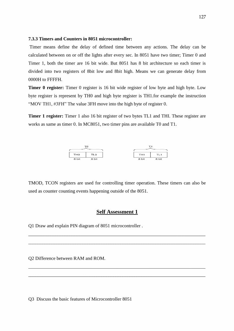
127
7.3.3 Timers and Counters in 8051 microcontroller:
Timer means define the delay of defined time between any actions. The delay can be
calculated between on or off the lights after every sec. In 8051 have two timer; Timer 0 and
Timer 1, both the timer are 16 bit wide. But 8051 has 8 bit architecture so each timer is
divided into two registers of 8bit low and 8bit high. Means we can generate delay from
0000H to FFFFH.
Timer 0 register: Timer 0 register is 16 bit wide register of low byte and high byte. Low
byte register is represent by TH0 and high byte register is TH1.for example the instruction
“MOV TH1, #3FH” The value 3FH move into the high byte of register 0.
Timer 1 register: Timer 1 also 16 bit register of two bytes TL1 and THI. These register are
works as same as timer 0. In MC8051, two timer pins are available T0 and T1.
TMOD, TCON registers are used for controlling timer operation. These timers can also be
used as counter counting events happening outside of the 8051.
Self Assessment 1
Q1 Draw and explain PIN diagram of 8051 microcontroller .
___________________________________________________________________________
___________________________________________________________________________
Q2 Difference between RAM and ROM.
___________________________________________________________________________
___________________________________________________________________________
Q3 Discuss the basic features of Microcontroller 8051
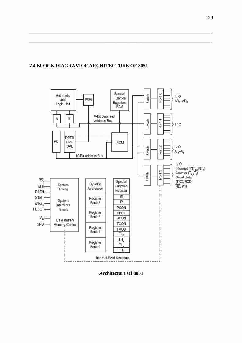
128
___________________________________________________________________________
___________________________________________________________________________
7.4 BLOCK DIAGRAM OF ARCHITECTURE OF 8051
Architecture Of 8051
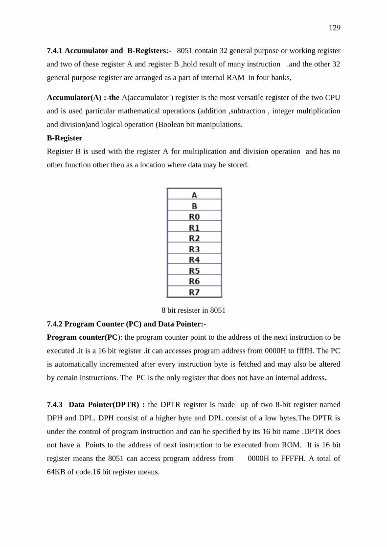
129
7.4.1 Accumulator and B-Registers:- 8051 contain 32 general purpose or working register
and two of these register A and register B ,hold result of many instruction .and the other 32
general purpose register are arranged as a part of internal RAM in four banks,
Accumulator(A) :-the A(accumulator ) register is the most versatile register of the two CPU
and is used particular mathematical operations (addition ,subtraction , integer multiplication
and division)and logical operation (Boolean bit manipulations.
B-Register
Register B is used with the register A for multiplication and division operation and has no
other function other then as a location where data may be stored.
8 bit resister in 8051
7.4.2 Program Counter (PC) and Data Pointer:-
Program counter(PC): the program counter point to the address of the next instruction to be
executed .it is a 16 bit register .it can accesses program address from 0000H to ffffH. The PC
is automatically incremented after every instruction byte is fetched and may also be altered
by certain instructions. The PC is the only register that does not have an internal address.
7.4.3 Data Pointer(DPTR) : the DPTR register is made up of two 8-bit register named
DPH and DPL. DPH consist of a higher byte and DPL consist of a low bytes.The DPTR is
under the control of program instruction and can be specified by its 16 bit name .DPTR does
not have a Points to the address of next instruction to be executed from ROM. It is 16 bit
register means the 8051 can access program address from 0000H to FFFFH. A total of
64KB of code.16 bit register means.
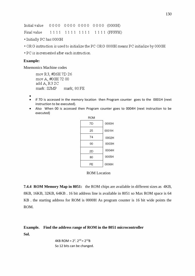
130
Example:
Mnemonics Machine codes
if 7D is accessed in the memory location then Program counter goes to the 0001H (next
instruction to be executed).
Also When 00 is accessed then Program counter goes to 0004H (next instruction to be executed)
ROM Location
7.4.4 ROM Memory Map in 8051: the ROM chips are available in different sizes as 4KB,
8KB, 16KB, 32KB, 64KB . 16 bit address line is available in 8051 so Max ROM space is 64
KB . the starting address for ROM is 0000H As program counter is 16 bit wide points the
ROM.
Example. Find the address range of ROM in the 8051 microcontroller
Sol.
4KB ROM = 22. 210 = 212B
So 12 bits can be changed.
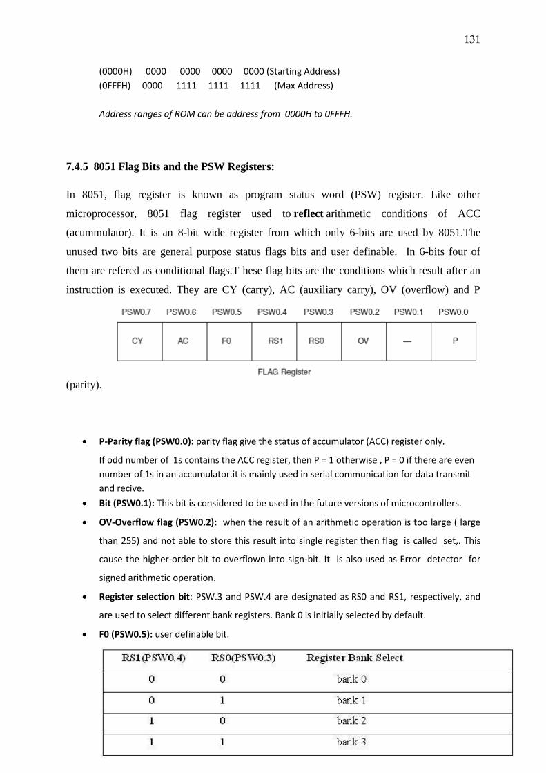
131
(0000H) 0000 0000 0000 0000 (Starting Address)
(0FFFH) 0000 1111 1111 1111 (Max Address)
Address ranges of ROM can be address from 0000H to 0FFFH.
7.4.5 8051 Flag Bits and the PSW Registers:
In 8051, flag register is known as program status word (PSW) register. Like other
microprocessor, 8051 flag register used to reflect arithmetic conditions of ACC
(acummulator). It is an 8-bit wide register from which only 6-bits are used by 8051.The
unused two bits are general purpose status flags bits and user definable. In 6-bits four of
them are refered as conditional flags.T hese flag bits are the conditions which result after an
instruction is executed. They are CY (carry), AC (auxiliary carry), OV (overflow) and P
(parity).
P-Parity flag (PSW0.0): parity flag give the status of accumulator (ACC) register only.
If odd number of 1s contains the ACC register, then P = 1 otherwise , P = 0 if there are even
number of 1s in an accumulator.it is mainly used in serial communication for data transmit
and recive.
Bit (PSW0.1): This bit is considered to be used in the future versions of microcontrollers.
OV-Overflow flag (PSW0.2): when the result of an arithmetic operation is too large ( large
than 255) and not able to store this result into single register then flag is called set,. This
cause the higher-order bit to overflown into sign-bit. It is also used as Error detector for
signed arithmetic operation.
Register selection bit: PSW.3 and PSW.4 are designated as RS0 and RS1, respectively, and
are used to select different bank registers. Bank 0 is initially selected by default.
F0 (PSW0.5): user definable bit.
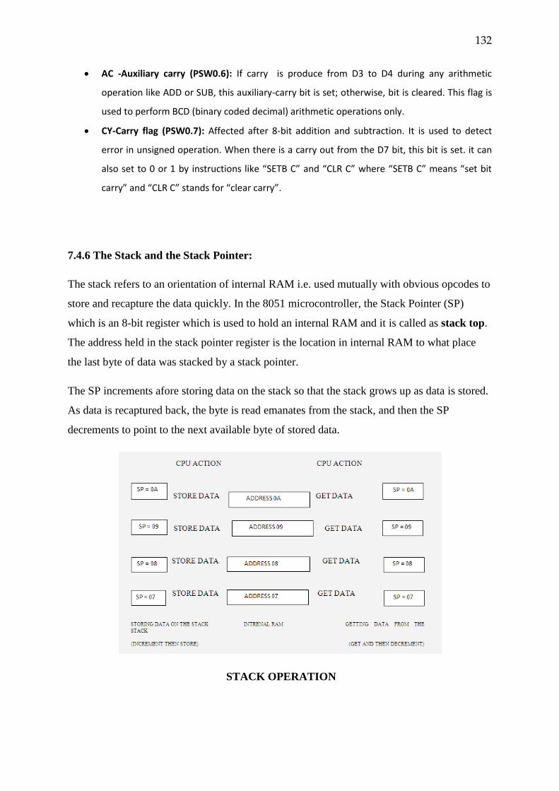
132
AC -Auxiliary carry (PSW0.6): If carry is produce from D3 to D4 during any arithmetic
operation like ADD or SUB, this auxiliary-carry bit is set; otherwise, bit is cleared. This flag is
used to perform BCD (binary coded decimal) arithmetic operations only.
CY-Carry flag (PSW0.7): Affected after 8-bit addition and subtraction. It is used to detect
error in unsigned operation. When there is a carry out from the D7 bit, this bit is set. it can
also set to 0 or 1 by instructions like “SETB C” and “CLR C” where “SETB C” means “set bit
carry” and “CLR C” stands for “clear carry”.
7.4.6 The Stack and the Stack Pointer:
The stack refers to an orientation of internal RAM i.e. used mutually with obvious opcodes to
store and recapture the data quickly. In the 8051 microcontroller, the Stack Pointer (SP)
which is an 8-bit register which is used to hold an internal RAM and it is called as stack top.
The address held in the stack pointer register is the location in internal RAM to what place
the last byte of data was stacked by a stack pointer.
The SP increments afore storing data on the stack so that the stack grows up as data is stored.
As data is recaptured back, the byte is read emanates from the stack, and then the SP
decrements to point to the next available byte of stored data.
STACK OPERATION
133
The stack pointer and the operation of stack is shown in Fig. .a. The stack pointer is set to
07H when 8051 is reset and can be converted to any internal RAM address by the user. The
stack is definite is height to the size of the internal RAM. The stack has the potential to over-
indite useful data in the register banks, bit-addressable and scratch-pad RAM areas. The user
is responsible for ascertaining that the stack does not grow beyond pre-defined bounds. The
stack is typically placed high in internal RAM, by a convenient choice of the number placed
in the stack pointer register, to avert conflicts with register-bit and scratch-pad internal RAM
operations.
Example:
The stack pointer is incremented by one after each PUSH instruction while in microcontroller
stack pointer is decremented after PUSH instruction. The stack pointer is decremented after
each POP instruction.
Self Assessment 2
Q1 Explain the 16 bit Register DPTR?
Q2 Discuss the function of accumulator in 8051.
Q3 Write a short note on 8051 Flag Bits .
Q4 write the fucvtion of Psen Pin.
Answers to Check Your Progress/Suggested Answers to SAQ
Self Assessment 1
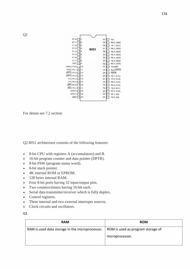
134
Q1
For detain see 7.2 section
Q2 8051 architecture consists of the following features:
8-bit CPU with registers A (accumulators) and B.
16-bit program counter and data pointer (DPTR).
8-bit PSW (program status word).
8-bit stack pointer.
4K internal ROM or EPROM.
128 bytes internal RAM.
Four 8-bit ports having 32 input/output pins.
Two counters/timers having 16-bit each.
Serial data transmitter/receiver which is fully duplex.
Control registers.
Three internal and two external interrupts sources.
Clock circuits and oscillators.
Q3
RAM ROM
RAM is used data storage in the microprocessor.
ROM is used as program storage of
microprocessor.
135
RAM is non volatile memory i.e. its contents are
lost when the device is powered off.
The price of RAMs are comparatively high The
price
it assist the processor to boost up the speed as
the RAM is faster
Type of RAM: Static RAM, Dynamic RAM
ROM is volatile memory i.e. its contents are
retained even when the device is powered off.
The price of ROMs are comparatively low
ROM cannot boost up the processor speed as
Speed of ROM is slower in comparison with
RAM,
Type of ROM: PROM, EPROM , EEPROM
Self Assessment 2
Q1 Data Pointer(DPTR) : the DPTR register is made up of two 8-bit register named DPH
and DPL. DPH consist of a higher byte and DPL consist of a low bytes.The DPTR is under
the control of program instruction and can be specified by its 16 bit name .DPTR does not
have a sing
• Points to the address of next instruction to be executed from ROM
• It is 16 bit register means the 8051 can access program address from
0000H to FFFFH. A total of 64KB of code.16 bit register means.
Initial value 0 0 0 0 0 0 0 0 0 0 0 0 0 0 0 0 (0000H)
Final value 1 1 1 1 1 1 1 1 1 1 1 1 1 1 1 1 (FFFFH)
• Initially PC has 0000H
• ORG instruction is used to initialize the PC ORG 0000H means PC initialize by 0000H
• PC is incremented after each instruction.
Q2 Accumulator(A) :-the A(accumulator ) register is the most versatile register of the two
CPU and is used particular mathematical operations (addition ,subtraction , integer
multiplication and division)and logical operation (Boolean bit manipulations.
Q3 8051 Flag Bits and the PSW Registers:
In 8051, flag register is known as program status word (PSW) register. Like other
microprocessor, 8051 flag register used to reflect arithmetic conditions of ACC
136
(acummulator). It is an 8-bit wide register from which only 6-bits are used by 8051.The
unused two bits are general purpose status flags bits and user definable. In 6-bits four of them
are refered as conditional flags.These flag bits indicate some conditions that result after an
instruction is executed. They are CY (carry), AC (auxiliary carry), OV (overflow) and P
(parity).
P-Parity flag (PSW0.0): parity flag reflects the status of accumulator(ACC) register only.
If the ACC register contains an odd number of 1s, then P = 1 otherwise , P = 0 if there are
even number of 1s in an accumulator.it is mainly used in serial communication for data
transmit and recive.
Bit (PSW0.1): This bit is considered to be used in the future versions of microcontrollers.
OV-Overflow flag (PSW0.2): This flag is set when the result of an arithmatic operation is too
large ( large than 255), and not able to store this result into single register. This cause the
higher-order bit to overflown into sign-bit.This is used to detect error in signed arithmatic
operation. This is similar to carry flag but difference is only that carry flag is used for
unsigned operations.
Register selection bit: PSW.3 and PSW.4 are designated as RS0 and RS1, respectively, and
are used to select different bank registers. Bank 0 is initialy selected by default.
RS1(PSW0.4) RS0(PSW0.3) Register Bank Select
0 0 bank 0
0 1 bank 1
1 0 bank 2
1 1 bank 3
F0 (PSW0.5): user definable bit.
AC -Auxiliary carry (PSW0.6): If carry is produce from D3 to D4 during any airthmatic
operation like ADD or SUB, this auxiliary-carry bit is set; otherwise,bit is cleared. This flag is
used to perform BCD (binary coded decimal) arithmetic operations only.
CY-Carry flag (PSW0.7): Affected after 8-bit addition and substraction. It is used to detect
error in unsigned operation.When there is a carry out from the D7 bit,this bit is set.it can
also set to 0 or 1 by instructions like “SETB C” and “CLR C” where “SETB C” means “set bit
carry” and “CLR C” stands for “clear carry”.
Q4 PSEN – (Program store enable) the PSEN is 29 pin of 8051. PSEN pin is the output
signal and connect to OE pin of ROM containing the program code. This pin use for to access
the access the external ROM. In 8051 microcontroller EA pin is connected to ground and
137
PSEN pin activate. In 8751 microcontroller EA pin is connected to VCC and PSEN pin do
not activate. This pin is active low.
138
Chapter 8
Programming and Interfacing with 8051
microcontroller
STRUCTURE
8.0 Objectives
8.1 Instruction Set
Logic Instruction
SFR Bit Addresses
Bit -Level Boolean Operations
Arithmetic instructions
8.2 Interface Push Button Switch
8.3 Interfacing LED to Microcontroller
8.4 Interfacing Seven Segment Display to Microcontroller
8.5 Interfacing LCD to Microcontroller
8.6 Interfacing Analog to Digital Convertor
8.7 Interfacing Keypad with 8051
8.8 Interfacing Stepper Motor with 8051
OBJECTIVES After studying this chapter you will understand
Instruction Set :Logic Instruction, SFR Bit Addresses, Bit -Level Boolean Operations,
Arithmetic instructions
Interface Push Button Switch ,
Interfacing LED to Microcontroller
Interfacing Seven Segment Display to Microcontroller
Interfacing LCD to Microcontroller
Interfacing Analog to Digital Convertor
Interfacing Keypad with 8051
Interfacing Stepper Motor with 8051
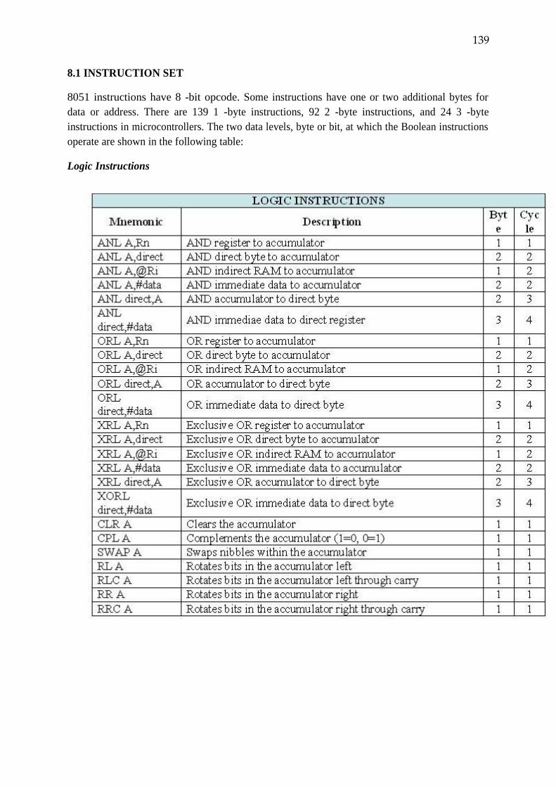
139
8.1 INSTRUCTION SET
8051 instructions have 8 -bit opcode. Some instructions have one or two additional bytes for
data or address. There are 139 1 -byte instructions, 92 2 -byte instructions, and 24 3 -byte
instructions in microcontrollers. The two data levels, byte or bit, at which the Boolean instructions
operate are shown in the following table:
Logic Instructions
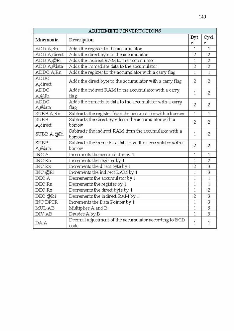
140
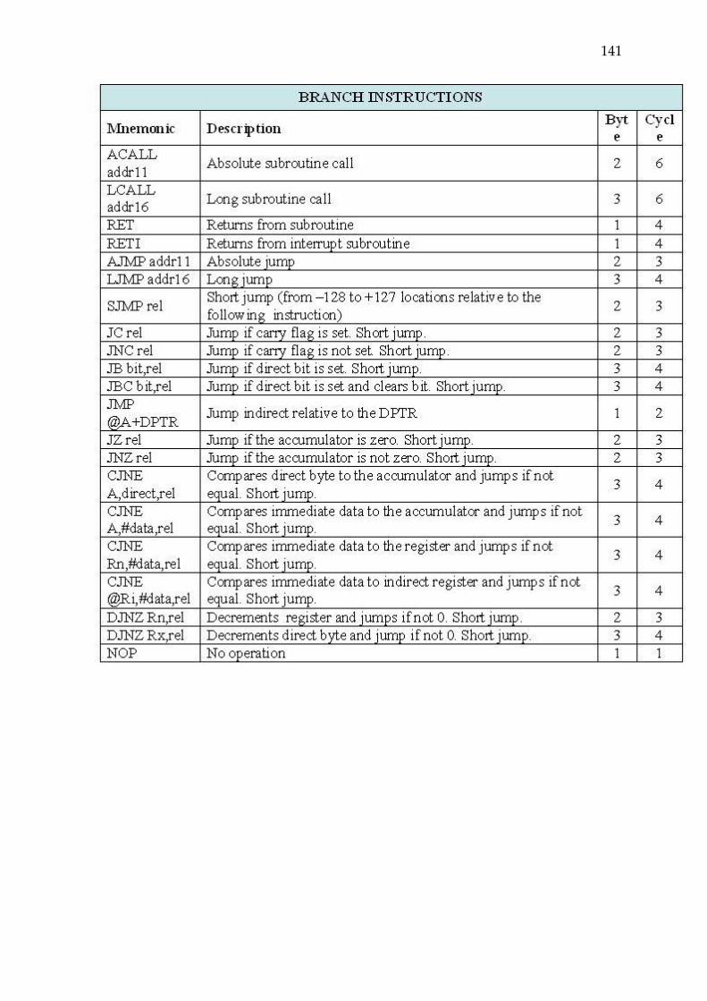
141
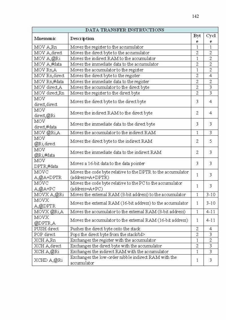
142
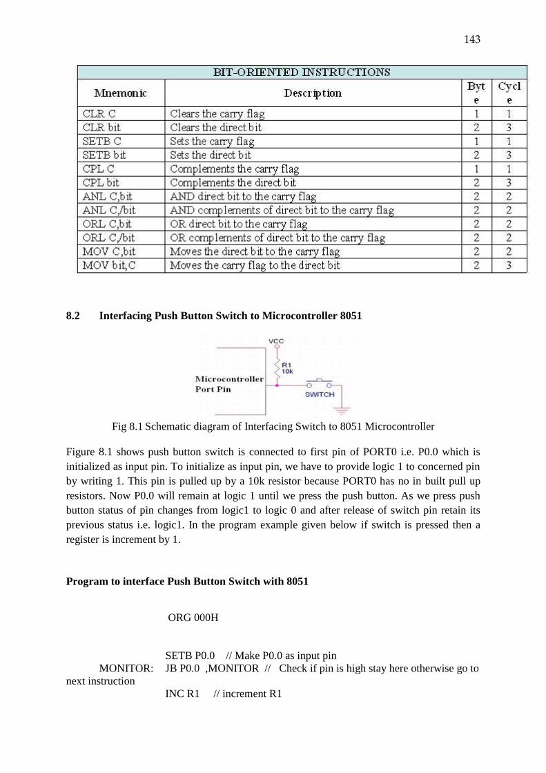
143
8.2 Interfacing Push Button Switch to Microcontroller 8051
Fig 8.1 Schematic diagram of Interfacing Switch to 8051 Microcontroller
Figure 8.1 shows push button switch is connected to first pin of PORT0 i.e. P0.0 which is
initialized as input pin. To initialize as input pin, we have to provide logic 1 to concerned pin
by writing 1. This pin is pulled up by a 10k resistor because PORT0 has no in built pull up
resistors. Now P0.0 will remain at logic 1 until we press the push button. As we press push
button status of pin changes from logic1 to logic 0 and after release of switch pin retain its
previous status i.e. logic1. In the program example given below if switch is pressed then a
register is increment by 1.
Program to interface Push Button Switch with 8051
ORG 000H
SETB P0.0 // Make P0.0 as input pin
MONITOR: JB P0.0 ,MONITOR // Check if pin is high stay here otherwise go to
next instruction
INC R1 // increment R1
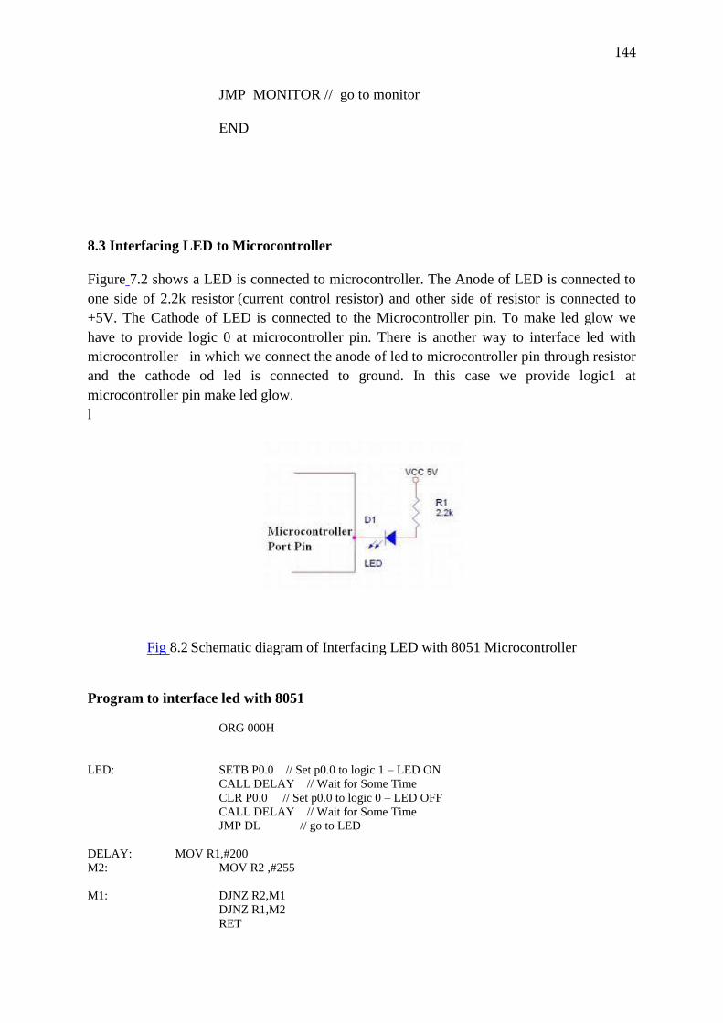
144
JMP MONITOR // go to monitor
END
8.3 Interfacing LED to Microcontroller
Figure 7.2 shows a LED is connected to microcontroller. The Anode of LED is connected to
one side of 2.2k resistor (current control resistor) and other side of resistor is connected to
+5V. The Cathode of LED is connected to the Microcontroller pin. To make led glow we
have to provide logic 0 at microcontroller pin. There is another way to interface led with
microcontroller in which we connect the anode of led to microcontroller pin through resistor
and the cathode od led is connected to ground. In this case we provide logic1 at
microcontroller pin make led glow.
l
Fig 8.2 Schematic diagram of Interfacing LED with 8051 Microcontroller
Program to interface led with 8051
ORG 000H
LED: SETB P0.0 // Set p0.0 to logic 1 – LED ON
CALL DELAY // Wait for Some Time
CLR P0.0 // Set p0.0 to logic 0 – LED OFF
CALL DELAY // Wait for Some Time
JMP DL // go to LED
DELAY: MOV R1,#200
M2: MOV R2 ,#255
M1: DJNZ R2,M1
DJNZ R1,M2
RET
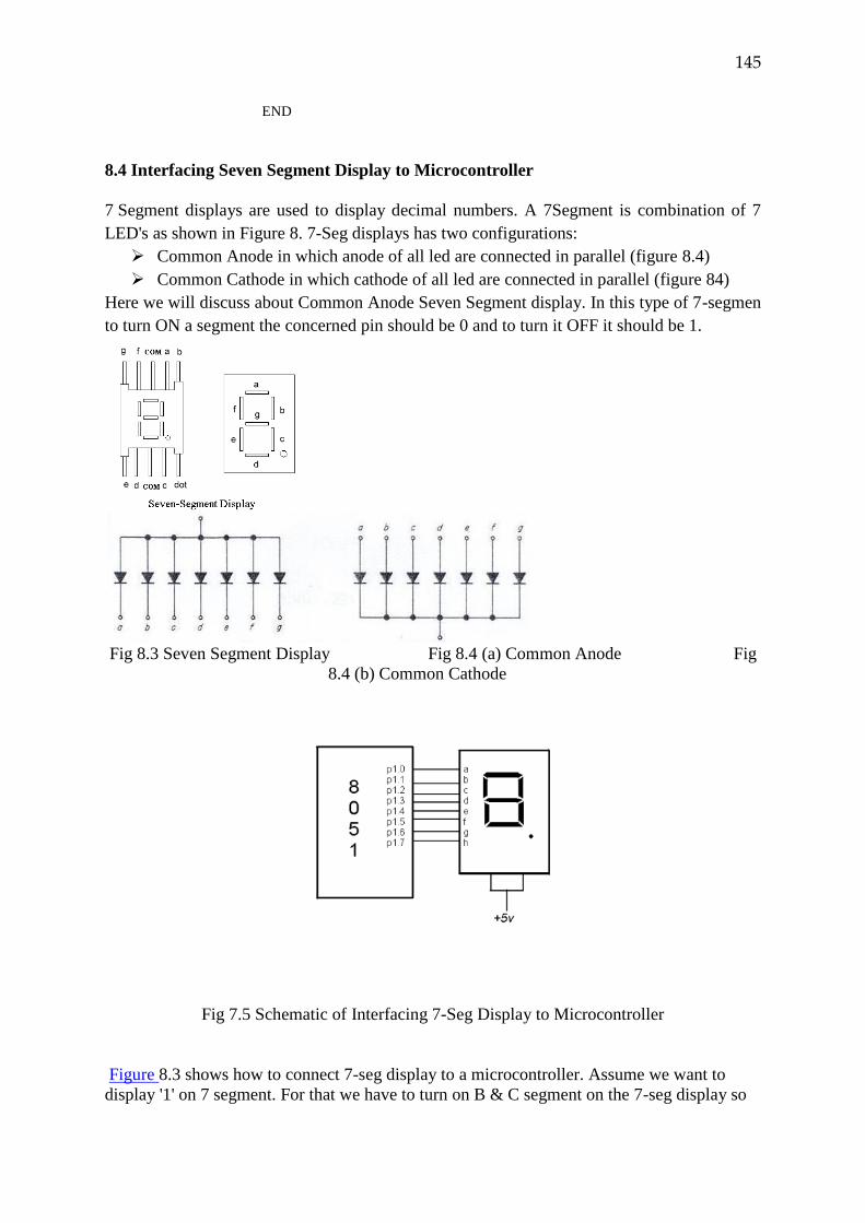
145
END
8.4 Interfacing Seven Segment Display to Microcontroller
7 Segment displays are used to display decimal numbers. A 7Segment is combination of 7
LED's as shown in Figure 8. 7-Seg displays has two configurations:
Common Anode in which anode of all led are connected in parallel (figure 8.4)
Common Cathode in which cathode of all led are connected in parallel (figure 84)
Here we will discuss about Common Anode Seven Segment display. In this type of 7-segmen
to turn ON a segment the concerned pin should be 0 and to turn it OFF it should be 1.
Fig 8.3 Seven Segment Display Fig 8.4 (a) Common Anode Fig
8.4 (b) Common Cathode
Fig 7.5 Schematic of Interfacing 7-Seg Display to Microcontroller
Figure 8.3 shows how to connect 7-seg display to a microcontroller. Assume we want to
display '1' on 7 segment. For that we have to turn on B & C segment on the 7-seg display so
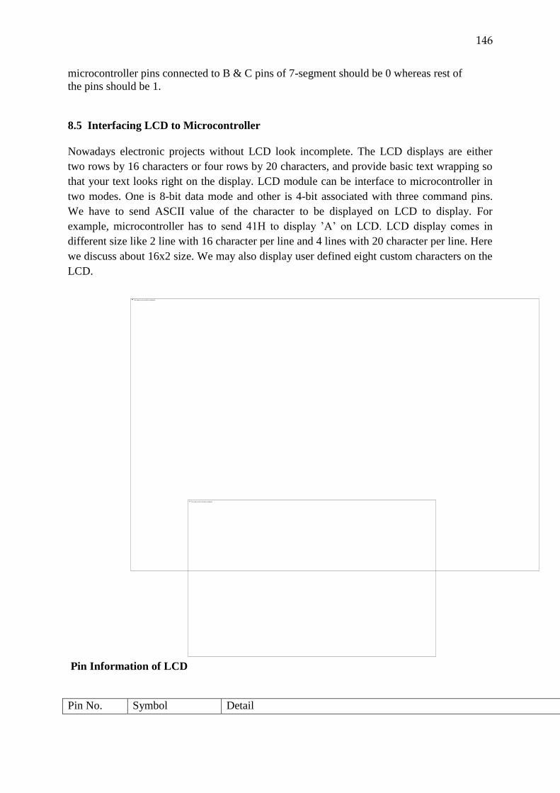
146
microcontroller pins connected to B & C pins of 7-segment should be 0 whereas rest of
the pins should be 1.
8.5 Interfacing LCD to Microcontroller
Nowadays electronic projects without LCD look incomplete. The LCD displays are either
two rows by 16 characters or four rows by 20 characters, and provide basic text wrapping so
that your text looks right on the display. LCD module can be interface to microcontroller in
two modes. One is 8-bit data mode and other is 4-bit associated with three command pins.
We have to send ASCII value of the character to be displayed on LCD to display. For
example, microcontroller has to send 41H to display ’A’ on LCD. LCD display comes in
different size like 2 line with 16 character per line and 4 lines with 20 character per line. Here
we discuss about 16x2 size. We may also display user defined eight custom characters on the
LCD.
Pin Information of LCD
Pin No. Symbol Detail
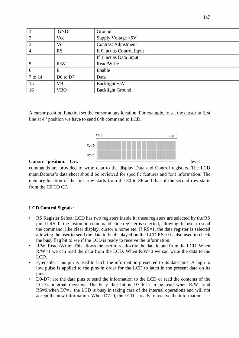
147
1 GND Ground
2 Vcc Supply Voltage +5V
3 Vo Contrast Adjustment
4 RS If 0, act as Control Input
If 1, act as Data Input
5 R/W Read/Write
6 E Enable
7 to 14 D0 to D7 Data
15 VBI Backlight +5V
16 VBO Backlight Ground
A cursor position function set the cursor at any location. For example, to set the cursor in first
line at 4th position we have to send 84h command to LCD.
Cursor position: Low- level
commands are provided to write data to the display Data and Control registers. The LCD
manufacturer’s data sheet should be reviewed for specific features and font information. The
memory location of the first row starts from the 80 to 8F and that of the second row starts
from the C0 TO CF.
LCD Control Signals:
• RS Register Select: LCD has two registers inside it; these registers are selected by the RS
pin. If RS=0, the instruction command code register is selected, allowing the user to send
the command, like clear display, cursor a home etc. If RS=1, the data register is selected
allowing the user to send the data to be displayed on the LCD.RS=0 is also used to check
the busy flag bit to see if the LCD is ready to receive the information.
• R/W, Read /Write: This allows the user to read/write the data in and from the LCD. When
R/W=1 we can read the data from the LCD. When R/W=0 we can write the data to the
LCD.
• E, enable: This pin is used to latch the information presented to its data pins. A high to
low pulse is applied to the pins in order for the LCD to latch in the present data on its
pins.
• D0-D7: are the data pins to send the information to the LCD or read the contents of the
LCD’s internal registers. The busy flag bit is D7 bit can be read when R/W=1and
RS=0.when D7=1, the LCD is busy in taking care of the internal operations and will not
accept the new information. When D7=0, the LCD is ready to receive the information.
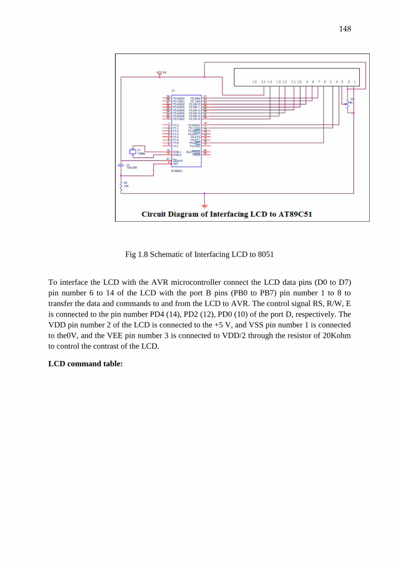
148
Fig 1.8 Schematic of Interfacing LCD to 8051
To interface the LCD with the AVR microcontroller connect the LCD data pins (D0 to D7)
pin number 6 to 14 of the LCD with the port B pins (PB0 to PB7) pin number 1 to 8 to
transfer the data and commands to and from the LCD to AVR. The control signal RS, R/W, E
is connected to the pin number PD4 (14), PD2 (12), PD0 (10) of the port D, respectively. The
VDD pin number 2 of the LCD is connected to the +5 V, and VSS pin number 1 is connected
to the0V, and the VEE pin number 3 is connected to VDD/2 through the resistor of 20Kohm
to control the contrast of the LCD.
LCD command table:
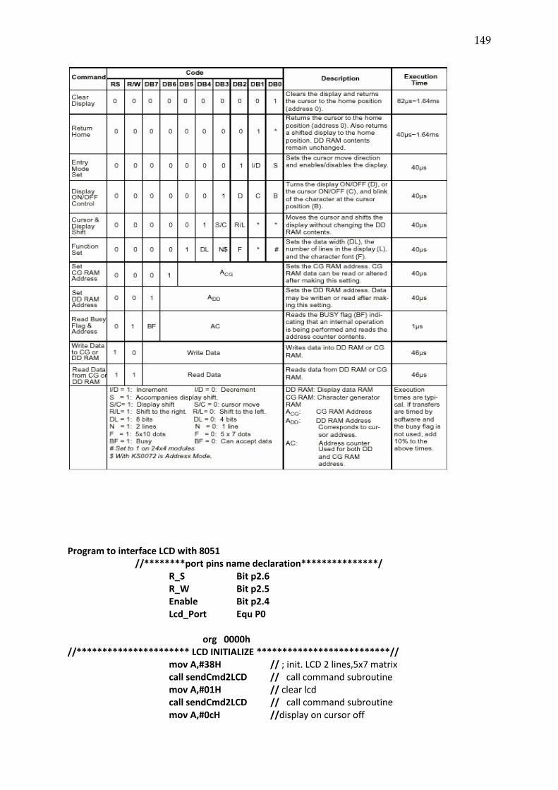
149
Program to interface LCD with 8051
//********port pins name declaration***************/ R_S Bit p2.6 R_W Bit p2.5 Enable Bit p2.4 Lcd_Port Equ P0
org 0000h
//********************** LCD INITIALIZE **************************// mov A,#38H // ; init. LCD 2 lines,5x7 matrix call sendCmd2LCD // call command subroutine mov A,#01H // clear lcd call sendCmd2LCD // call command subroutine mov A,#0cH //display on cursor off
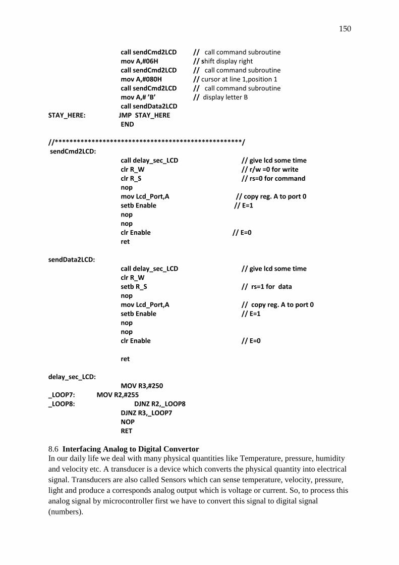
150
call sendCmd2LCD // call command subroutine mov A,#06H // shift display right call sendCmd2LCD // call command subroutine
mov A,#080H // cursor at line 1,position 1 call sendCmd2LCD // call command subroutine mov A,# ’B’ // display letter B call sendData2LCD STAY_HERE: JMP STAY_HERE END //***************************************************/ sendCmd2LCD: call delay_sec_LCD // give lcd some time clr R_W // r/w =0 for write clr R_S // rs=0 for command nop mov Lcd_Port,A // copy reg. A to port 0 setb Enable // E=1 nop nop clr Enable // E=0 ret sendData2LCD: call delay_sec_LCD // give lcd some time clr R_W setb R_S // rs=1 for data nop mov Lcd_Port,A // copy reg. A to port 0 setb Enable // E=1 nop nop clr Enable // E=0 ret delay_sec_LCD: MOV R3,#250 _LOOP7: MOV R2,#255 _LOOP8: DJNZ R2,_LOOP8 DJNZ R3,_LOOP7 NOP RET
8.6 Interfacing Analog to Digital Convertor
In our daily life we deal with many physical quantities like Temperature, pressure, humidity
and velocity etc. A transducer is a device which converts the physical quantity into electrical
signal. Transducers are also called Sensors which can sense temperature, velocity, pressure,
light and produce a corresponds analog output which is voltage or current. So, to process this
analog signal by microcontroller first we have to convert this signal to digital signal
(numbers).
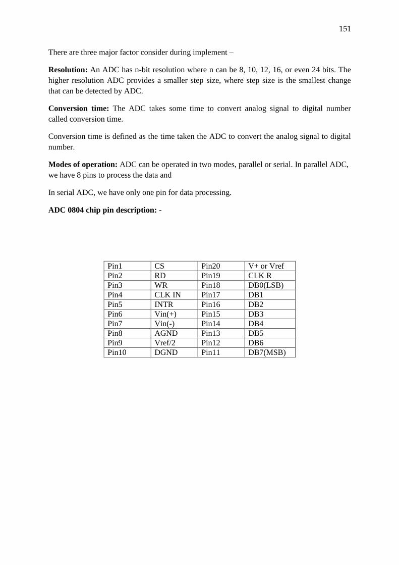
151
There are three major factor consider during implement –
Resolution: An ADC has n-bit resolution where n can be 8, 10, 12, 16, or even 24 bits. The
higher resolution ADC provides a smaller step size, where step size is the smallest change
that can be detected by ADC.
Conversion time: The ADC takes some time to convert analog signal to digital number
called conversion time.
Conversion time is defined as the time taken the ADC to convert the analog signal to digital
number.
Modes of operation: ADC can be operated in two modes, parallel or serial. In parallel ADC,
we have 8 pins to process the data and
In serial ADC, we have only one pin for data processing.
ADC 0804 chip pin description: -
Pin1 CS Pin20 V+ or Vref
Pin2 RD Pin19 CLK R
Pin3 WR Pin18 DB0(LSB)
Pin4 CLK IN Pin17 DB1
Pin5 INTR Pin16 DB2
Pin6 Vin(+) Pin15 DB3
Pin7 Vin(-) Pin14 DB4
Pin8 AGND Pin13 DB5
Pin9 Vref/2 Pin12 DB6
Pin10 DGND Pin11 DB7(MSB)
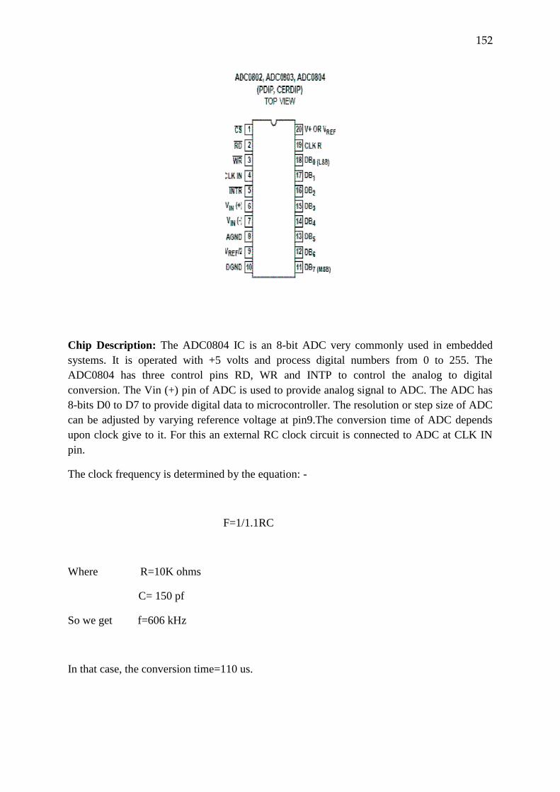
152
Chip Description: The ADC0804 IC is an 8-bit ADC very commonly used in embedded
systems. It is operated with +5 volts and process digital numbers from 0 to 255. The
ADC0804 has three control pins RD, WR and INTP to control the analog to digital
conversion. The Vin (+) pin of ADC is used to provide analog signal to ADC. The ADC has
8-bits D0 to D7 to provide digital data to microcontroller. The resolution or step size of ADC
can be adjusted by varying reference voltage at pin9.The conversion time of ADC depends
upon clock give to it. For this an external RC clock circuit is connected to ADC at CLK IN
pin.
The clock frequency is determined by the equation: -
F=1/1.1RC
Where R=10K ohms
C= 150 pf
So we get f=606 kHz
In that case, the conversion time=110 us.
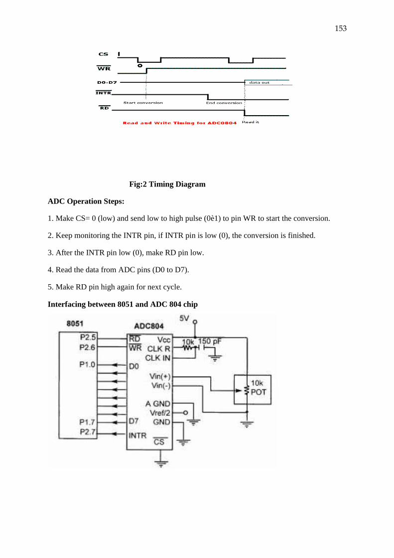
153
Fig:2 Timing Diagram
ADC Operation Steps:
1. Make CS= 0 (low) and send low to high pulse (0è1) to pin WR to start the conversion.
2. Keep monitoring the INTR pin, if INTR pin is low (0), the conversion is finished.
3. After the INTR pin low (0), make RD pin low.
4. Read the data from ADC pins (D0 to D7).
5. Make RD pin high again for next cycle.
Interfacing between 8051 and ADC 804 chip
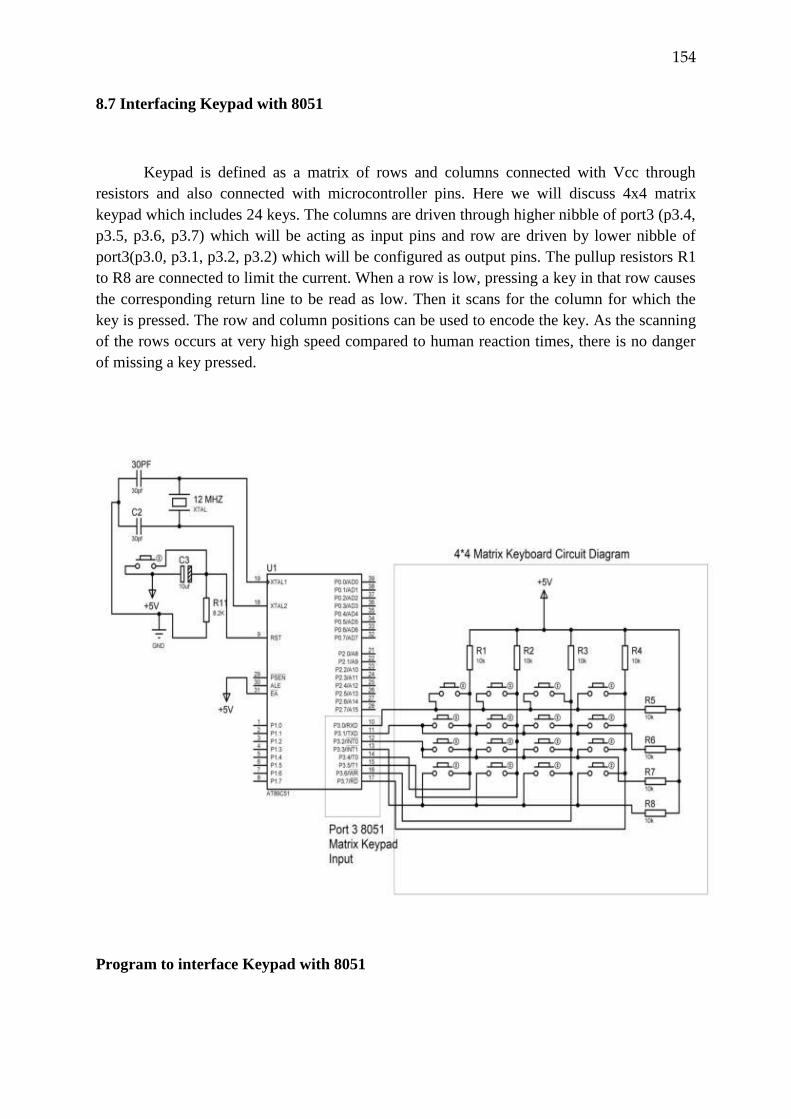
154
8.7 Interfacing Keypad with 8051
Keypad is defined as a matrix of rows and columns connected with Vcc through
resistors and also connected with microcontroller pins. Here we will discuss 4x4 matrix
keypad which includes 24 keys. The columns are driven through higher nibble of port3 (p3.4,
p3.5, p3.6, p3.7) which will be acting as input pins and row are driven by lower nibble of
port3(p3.0, p3.1, p3.2, p3.2) which will be configured as output pins. The pullup resistors R1
to R8 are connected to limit the current. When a row is low, pressing a key in that row causes
the corresponding return line to be read as low. Then it scans for the column for which the
key is pressed. The row and column positions can be used to encode the key. As the scanning
of the rows occurs at very high speed compared to human reaction times, there is no danger
of missing a key pressed.
Program to interface Keypad with 8051
155
// ******** KEYPAD PROGRAM ********** // //******** P0.0-- P0.3 are connected to columns ****** //******** p2.0-- p2.2 are connected to rows ******* keypad: mov p0,#0ffh ; make p0 input port check : mov p2,#00 ; ground all rows mov a,p0 anl a,#00001111b ; mask upper 4 bits cjne a,#00001111b, check ; make sure all keys are open check_key: acall mili20 ; wait for 20ms mov a,p0 ; check if any switch pressed anl a,#00001111b cjne a,#00001111b,check_again ; switch pressed, wait sjmp check_key ;check if any switch pressed check_again: acall mili20 mov a,p0 anl a,#00001111b cjne a,#00001111b,searching ;switch pressed find row sjmp check_key ; if not keep monitoring searching : mov p2,#11111110b ; ground row 1 mov a,p0 ; read col. anl a,#00001111b cjne a,#00001111b,row_1 ; switch found in row 1, find column mov p2,#11111101b ; ground row 2 mov a,p0 ; read col. anl a,#00001111b cjne a,#00001111b,row_2 ; switch found in row 2, find column mov p2,#11111011b ; ground row 3 mov a,p0 anl a,#00001111b cjne a,#00001111b,row_3 ; switch found in row 3, find column
mov p2,#11110111b ; ground row 4 mov a,p0 anl a,#00001111b cjne a,#00001111b,row_4 ; switch found in row 4, find column ljmp check_key row_1 : mov dptr,#line1 ; set dptr at start of row1 sjmp find ; FIND COLOUMN KEY BLONGS TO row_2 : mov dptr,#line2 ; set dptr at start of row2 sjmp find row_3 : mov dptr,#line3 ; set dptr at start of row3 sjmp find row_4 : mov dptr,#line4 ; set dptr at start of row4
156
find : rrc a // see if any bit 0 jnc match // if 0 then get the value from table inc dptr sjmp find match : clr a movc a,@a+dptr mov p1,a ;; display pressed button on LCD ************* ljmp check ret mili20: mov r0,#20 again : mov r1,#255 here : djnz r1,here djnz r0,again ret //*************** LOOK UP TABLE****************// org 400h line1 : db '0','1','2','3' line2 : db '4','5','6','7' line3 : db '8','9','a','b' line3 : db 'c','d','e','f'
8.8 Interfacing Stepper Motor with 8051
A stepper motor is a device which accepts electrical pulses and make
mechanical movement. The stepper motor is used for precise angular movement and to
control position in many devices like printers, disc driver and robotics. In the stepper motor a
permanent magnet is surrounded by four stator windings as shown in figure below.
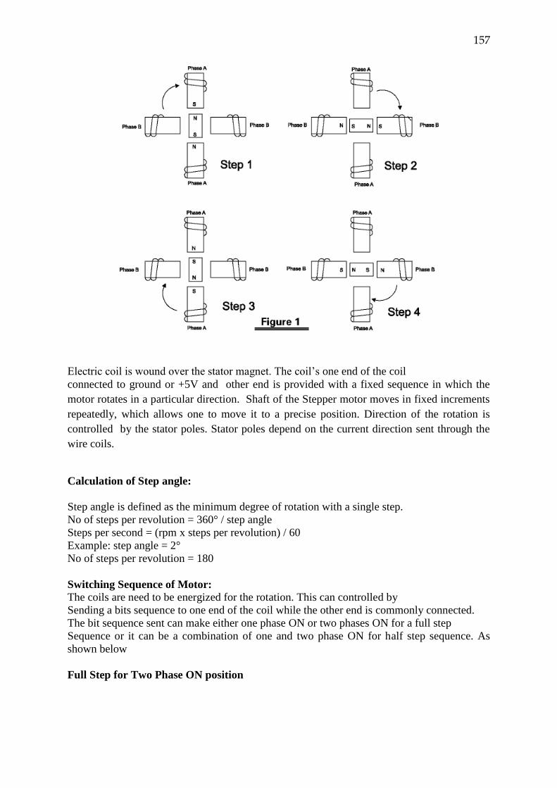
157
Electric coil is wound over the stator magnet. The coil’s one end of the coil
connected to ground or +5V and other end is provided with a fixed sequence in which the
motor rotates in a particular direction. Shaft of the Stepper motor moves in fixed increments
repeatedly, which allows one to move it to a precise position. Direction of the rotation is
controlled by the stator poles. Stator poles depend on the current direction sent through the
wire coils.
Calculation of Step angle:
Step angle is defined as the minimum degree of rotation with a single step.
No of steps per revolution = 360° / step angle
Steps per second = (rpm x steps per revolution) / 60
Example: step angle = 2°
No of steps per revolution = 180
Switching Sequence of Motor:
The coils are need to be energized for the rotation. This can controlled by
Sending a bits sequence to one end of the coil while the other end is commonly connected.
The bit sequence sent can make either one phase ON or two phases ON for a full step
Sequence or it can be a combination of one and two phase ON for half step sequence. As
shown below
Full Step for Two Phase ON position
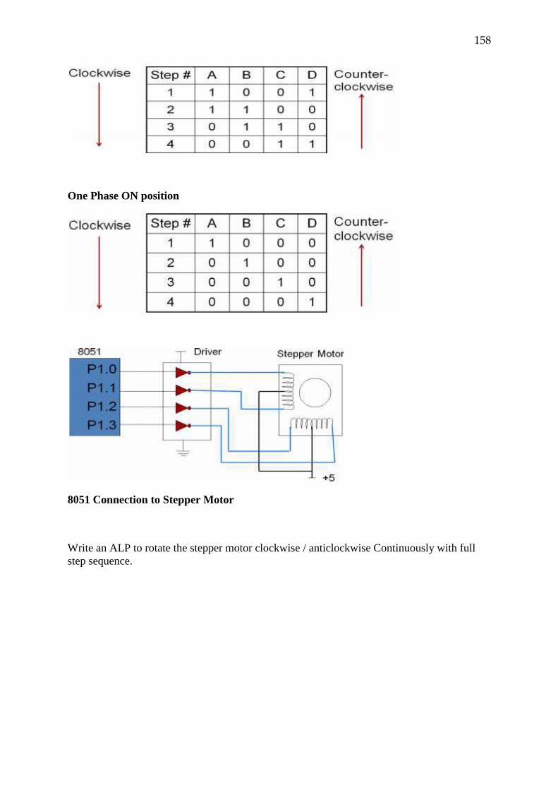
158
One Phase ON position
8051 Connection to Stepper Motor
Write an ALP to rotate the stepper motor clockwise / anticlockwise Continuously with full
step sequence.
159
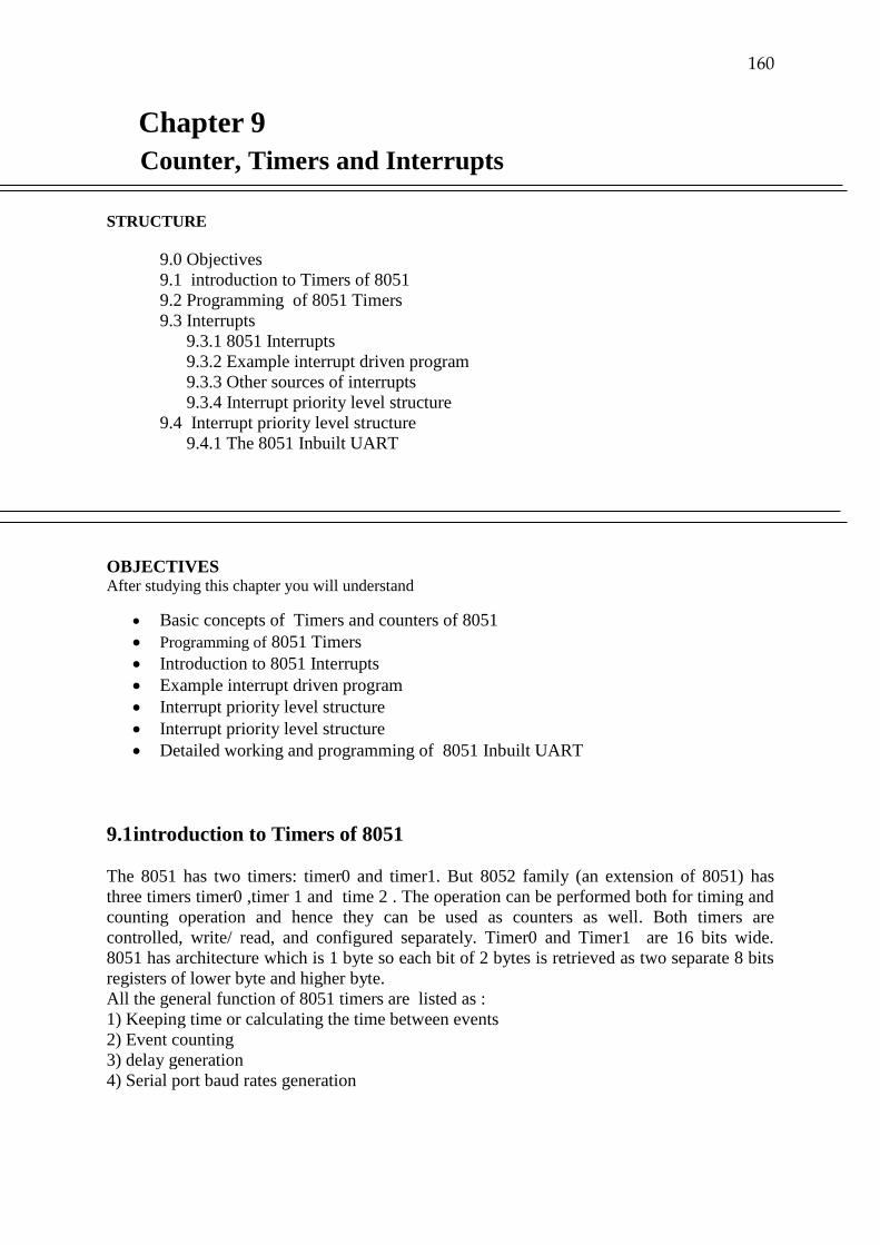
160
Chapter 9
Counter, Timers and Interrupts
STRUCTURE
9.0 Objectives
9.1 introduction to Timers of 8051
9.2 Programming of 8051 Timers
9.3 Interrupts
9.3.1 8051 Interrupts
9.3.2 Example interrupt driven program
9.3.3 Other sources of interrupts
9.3.4 Interrupt priority level structure
9.4 Interrupt priority level structure
9.4.1 The 8051 Inbuilt UART
OBJECTIVES After studying this chapter you will understand
Basic concepts of Timers and counters of 8051
Programming of 8051 Timers
Introduction to 8051 Interrupts
Example interrupt driven program
Interrupt priority level structure
Interrupt priority level structure
Detailed working and programming of 8051 Inbuilt UART
9.1 introduction to Timers of 8051
The 8051 has two timers: timer0 and timer1. But 8052 family (an extension of 8051) has
three timers timer0 ,timer 1 and time 2 . The operation can be performed both for timing and
counting operation and hence they can be used as counters as well. Both timers are
controlled, write/ read, and configured separately. Timer0 and Timer1 are 16 bits wide.
8051 has architecture which is 1 byte so each bit of 2 bytes is retrieved as two separate 8 bits
registers of lower byte and higher byte.
All the general function of 8051 timers are listed as :
1) Keeping time or calculating the time between events
2) Event counting
3) delay generation
4) Serial port baud rates generation
161
Calculating count for a timer
Firstly it is important to discuss that when a timer is in timer mode and properly
configured, the value of the timer register which is 16 bit long will be incremented by one per
machine cycle. A machine cycle is constituted by 12 clock pulse. Thus a running timer will
be incremented after a time:
12 / 12000000 = 0.000001second
1000000 times per second. some instruction are executed in 1 machine cycle, some
are in two machine cycles and others in four machine cycles. They will always be
incremented once per machine cycle. Let us suppose a timer has count of 0 to 50,000 then it
will be calculated as:
1 x10-6x50,000 = 0.05 s
Its unfruitful to know .05 s are passed. If we calculate this calculation in a reverse way by
knowing the time period and calculating the count of a timer.it is very useful for generating
an accurate delay for specific application. let us find out the value of count for time period of
100 micro second,
100x10-6/1x10-6=100
So if the counter counts 100 it will take 100x10-6 seconds at 12 MHz crystal frequency.
9.2 PROGRAMMING OF 8051 TIMERS
8051 architecture composes of two timers: Timer 0 and Timer 1. These timers 0 and 1
can be used as timers as well as counters. In the introduction we will first discuss the timer
registers and then we will use these timer register in a specific mode of operation to generate
an accurate time delay for specific application like baud rate generation.
Timer registers
The two timers, . Timer0 and Timer1 are 16 bits wide. 8051 has architecture which is 1 byte
so each bit of 2 bytes is retrieved as two separate 8 bits registers of lower byte and higher
byte.
Timer 0 registers
The 16 -bit register of timer 0 is available as lower- byte and higher byte . The low byte
register is called TL0 (Timer 0 lower byte ) and the register of higher byte is called TH0
(Timer 0 higher byte ) . These registers are opened like any other register, such as
Accumulator register , B, R0, Rl , R2 , etc.
For example, the instruction
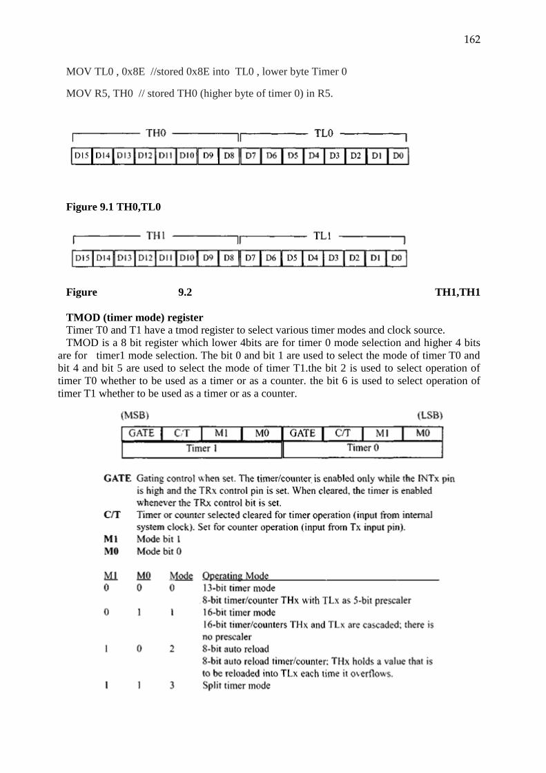
162
MOV TL0 , 0x8E //stored 0x8E into TL0 , lower byte Timer 0
MOV R5, TH0 // stored TH0 (higher byte of timer 0) in R5.
Figure 9.1 TH0,TL0
Figure 9.2 TH1,TH1
TMOD (timer mode) register
Timer T0 and T1 have a tmod register to select various timer modes and clock source.
TMOD is a 8 bit register which lower 4bits are for timer 0 mode selection and higher 4 bits
are for timer1 mode selection. The bit 0 and bit 1 are used to select the mode of timer T0 and
bit 4 and bit 5 are used to select the mode of timer T1.the bit 2 is used to select operation of
timer T0 whether to be used as a timer or as a counter. the bit 6 is used to select operation of
timer T1 whether to be used as a timer or as a counter.
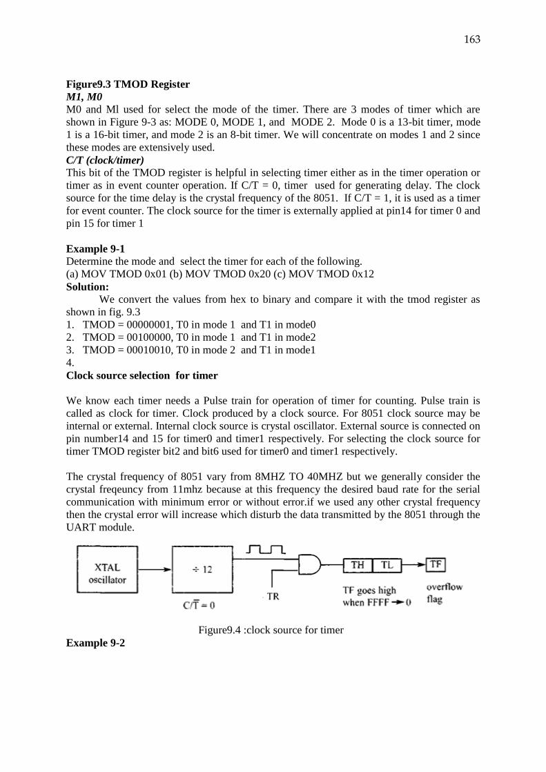
163
Figure9.3 TMOD Register
M1, M0 M0 and Ml used for select the mode of the timer. There are 3 modes of timer which are
shown in Figure 9-3 as: MODE 0, MODE 1, and MODE 2. Mode 0 is a 13-bit timer, mode
1 is a 16-bit timer, and mode 2 is an 8-bit timer. We will concentrate on modes 1 and 2 since
these modes are extensively used.
C/T (clock/timer) This bit of the TMOD register is helpful in selecting timer either as in the timer operation or
timer as in event counter operation. If C/T = 0, timer used for generating delay. The clock
source for the time delay is the crystal frequency of the 8051. If C/T = 1, it is used as a timer
for event counter. The clock source for the timer is externally applied at pin14 for timer 0 and
pin 15 for timer 1
Example 9-1 Determine the mode and select the timer for each of the following.
(a) MOV TMOD 0x01 (b) MOV TMOD 0x20 (c) MOV TMOD 0x12
Solution: We convert the values from hex to binary and compare it with the tmod register as
shown in fig. 9.3
1. TMOD = 00000001, T0 in mode 1 and T1 in mode0
2. TMOD = 00100000, T0 in mode 1 and T1 in mode2
3. TMOD = 00010010, T0 in mode 2 and T1 in mode1
4.
Clock source selection for timer
We know each timer needs a Pulse train for operation of timer for counting. Pulse train is
called as clock for timer. Clock produced by a clock source. For 8051 clock source may be
internal or external. Internal clock source is crystal oscillator. External source is connected on
pin number14 and 15 for timer0 and timer1 respectively. For selecting the clock source for
timer TMOD register bit2 and bit6 used for timer0 and timer1 respectively.
The crystal frequency of 8051 vary from 8MHZ TO 40MHZ but we generally consider the
crystal freqeuncy from 11mhz because at this frequency the desired baud rate for the serial
communication with minimum error or without error.if we used any other crystal frequency
then the crystal error will increase which disturb the data transmitted by the 8051 through the
UART module.
Figure9.4 :clock source for timer
Example 9-2
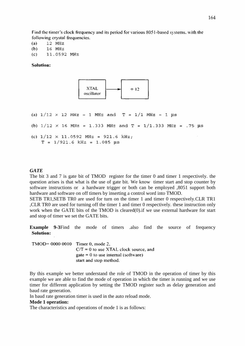
164
GATE
The bit 3 and 7 is gate bit of TMOD register for the timer 0 and timer 1 respectively. the
question arises is that what is the use of gate bit. We know timer start and stop counter by
software instructions or a hardware trigger or both can be employed ,8051 support both
hardware and software on off timers by inserting a control word into TMOD.
SETB TR1,SETB TR0 are used for turn on the timer 1 and timer 0 respectively.CLR TR1
,CLR TR0 are used for turning off the timer 1 and timer 0 respectively. these instruction only
work when the GATE bits of the TMOD is cleared(0).if we use external hardware for start
and stop of timer we set the GATE bits.
Example 9-3Find the mode of timers .also find the source of frequency
By this example we better understand the role of TMOD in the operation of timer by this
example we are able to find the mode of operation in which the timer is running and we use
timer for different application by setting the TMOD register such as delay generation and
baud rate generation.
In baud rate generation timer is used in the auto reload mode.
Mode 1 operation:
The characteristics and operations of mode 1 is as follows:
165
1. Mode 1 is 16bit timer mode. It counts from 0000H to FFFFH and the values are
loaded into two 8 bit registers TL and TH.
2. TH and TL are higher and lower 8 bit of timer counter register. After inserting the
value into these registers the timer is started while using the SETB TRx(x can be 0
or
3. As the timer starts counting it starts to increment the counter register (TH and
TL) per clock cycle of timer. The count limit is up to FFFFH. When this limit is
reached after one clock cycle the timer flag bit TF is set .
4. Once the timer flag bit is set; first we stop the timer and clear the flag bit by using
CLR TFx(x can be 0 or 1).then we repeat the process from step 2.
Procedure to follow to program timer in mode 1:
Mode 1 is generally used for generating the time delay, following steps are to be followed.
1. Load the TMOD register with correct control word which let the mode 1 for the timer.
2. Load the TL and TH with the desired count.
3. Start the timer and keep monitoring the timer flag while using JNB TFx(x can be 0 or
1).
4 when the TF is set stop the timer.
5. Using CLR instruction Clear the TF flag for the next round.
6. Repeat the step 2.
To calculate the exact tiem delay we must know the timer clcok period and count that is
loaded into TH TL Registers.
Formula for calculating the time delay
Time delay=((maximum count- inserting count )*12)/crystal frequency
(a) in hex (FFFF – count + 1) X clock time period of timer, where count are TH, TL initial values
respectively. Notice that values count are in hex.
(b) in decimal Convert count values of the TH,TL register to decimal to get a decimal number let which is
Y then (65536 – Y) x clock time period
Example 9-4 Write a program to generate a square wave of 50% duty cycle on pin P1.5
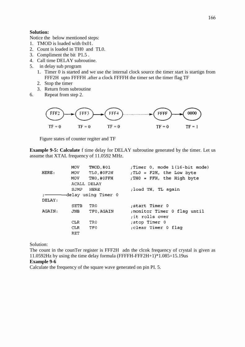
166
Solution: Notice the below mentioned steps:
1. TMOD is loaded with 0x01.
2. Count is loaded in TH0 and TL0.
3. Compliment the bit P1.5 .
4. Call time DELAY subroutine.
5. in delay sub program
1. Timer 0 is started and we use the internal clock source the timer start is startign from
FFF2H upto FFFFH .after a clock FFFFH the timer set the timer flag TF
2. Stop the timer
3. Return from subroutine
6. Repeat from step 2.
Figure states of counter regiter and TF
Example 9-5: Calculate f time delay for DELAY subroutine generated by the timer. Let us
assume that XTAL frequency of 11.0592 MHz.
Solution:
The count in the counTer register is FFF2H adn the clcok frequency of crystal is given as
11.0592Hz by using the time delay formula (FFFFH-FFF2H+1)*1.085=15.19us
Example 9-6 Calculate the frequency of the square wave generated on pin PI. 5.
167
Solution:
For calculating the frequency of square wave we must know how much a machine cycle is
take n by an instruction and how many instructions are to be used in subroutine of delay in
wave generation and we also know that frequency
Example 9-7 FIND THE time delay inproduced by the tiemr 0 in the following program.
For calculating time delay first we must the value of the count loaded into the term register
that is 0xB83E .
Now find how many times the timer increment set the tf flag by using following formula
(FFFF-B83E + 1) = 47C2H= 18370 in decimal
To find the time delay the count is to be multiplied with the time period of timer clock which
is ewual to 12/XTAL , so 18370 x 1.085 fis= 19.93145
ms.
Example 9-8
Find the delay in the following program
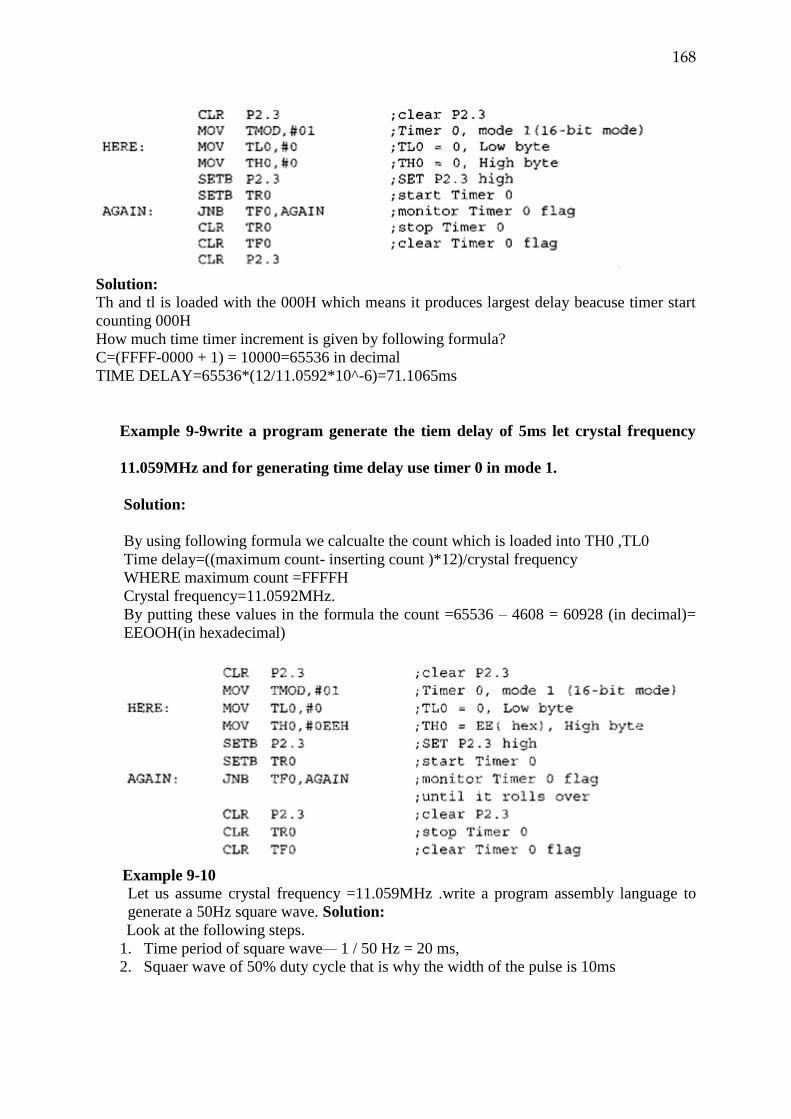
168
Solution: Th and tl is loaded with the 000H which means it produces largest delay beacuse timer start
counting 000H
How much time timer increment is given by following formula?
C=(FFFF-0000 + 1) = 10000=65536 in decimal
TIME DELAY=65536*(12/11.0592*10^-6)=71.1065ms
Example 9-9write a program generate the tiem delay of 5ms let crystal frequency
11.059MHz and for generating time delay use timer 0 in mode 1.
Solution:
By using following formula we calcualte the count which is loaded into TH0 ,TL0
Time delay=((maximum count- inserting count )*12)/crystal frequency
WHERE maximum count =FFFFH
Crystal frequency=11.0592MHz.
By putting these values in the formula the count =65536 – 4608 = 60928 (in decimal)=
EEOOH(in hexadecimal)
Example 9-10 Let us assume crystal frequency =11.059MHz .write a program assembly language to
generate a 50Hz square wave. Solution:
Look at the following steps.
1. Time period of square wave— 1 / 50 Hz = 20 ms,
2. Squaer wave of 50% duty cycle that is why the width of the pulse is 10ms
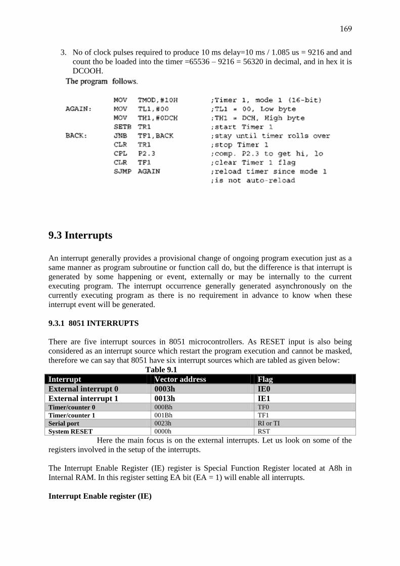
169
3. No of clock pulses required to produce 10 ms delay=10 ms / 1.085 us = 9216 and and
count tho be loaded into the timer =65536 – 9216 = 56320 in decimal, and in hex it is
DCOOH.
9.3 Interrupts
An interrupt generally provides a provisional change of ongoing program execution just as a
same manner as program subroutine or function call do, but the difference is that interrupt is
generated by some happening or event, externally or may be internally to the current
executing program. The interrupt occurrence generally generated asynchronously on the
currently executing program as there is no requirement in advance to know when these
interrupt event will be generated.
9.3.1 8051 INTERRUPTS
There are five interrupt sources in 8051 microcontrollers. As RESET input is also being
considered as an interrupt source which restart the program execution and cannot be masked,
therefore we can say that 8051 have six interrupt sources which are tabled as given below:
Table 9.1
Interrupt Vector address Flag
External interrupt 0 0003h IE0
External interrupt 1 0013h IE1
Timer/counter 0 000Bh TF0
Timer/counter 1 001Bh TF1
Serial port 0023h RI or TI
System RESET 0000h RST
Here the main focus is on the external interrupts. Let us look on some of the
registers involved in the setup of the interrupts.
The Interrupt Enable Register (IE) register is Special Function Register located at A8h in
Internal RAM. In this register setting EA bit (EA = 1) will enable all interrupts.
Interrupt Enable register (IE)
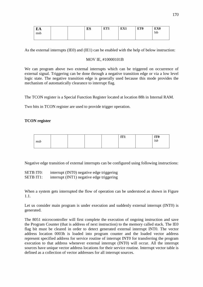
170
As the external interrupts (IE0) and (IE1) can be enabled with the help of below instruction:
MOV IE, #10000101B
We can program above two external interrupts which can be triggered on occurrence of
external signal. Triggering can be done through a negative transition edge or via a low level
logic state. The negative transition edge is generally used because this mode provides the
mechanism of automatically clearance to interrupt flag.
The TCON register is a Special Function Register located at location 88h in Internal RAM.
Two bits in TCON register are used to provide trigger operation.
TCON register
Negative edge transition of external interrupts can be configured using following instructions:
SETB IT0: interrupt (INT0) negative edge triggering
SETB IT1: interrupt (INT1) negative edge triggering
When a system gets interrupted the flow of operation can be understood as shown in Figure
1.1.
Let us consider main program is under execution and suddenly external interrupt (INT0) is
generated.
The 8051 microcontroller will first complete the execution of ongoing instruction and save
the Program Counter (that is address of next instruction) to the memory called stack. The IE0
flag bit must be cleared in order to detect generated external interrupt INT0. The vector
address location 0003h is loaded into program counter and the loaded vector address
represent specified address for service routine of interrupt INT0 for transferring the program
execution to that address whenever external interrupt (INT0) will occur. All the interrupt
sources have unique vector address locations for their service routine. Interrupt vector table is
defined as a collection of vector addresses for all interrupt sources.
EA msb
ES ET1 EX1 ET0 EX0
lsb
msb
IT1 IT0
lsb
171
LJMP instruction is used to transfer the flow of program to specified vector address location
for the corresponding ISR (Interrupt Service Routine).
The ISR routine is defined by the programmer in order to service the interrupt event
whenever it occurs. So at the occurrence of interrupt event, a good programmer will save the
registers (That is PUSH Operation) and also at the end of Interrupt Service this registers are
restored (that is POP Operation), thus this habit provides registers preservations.
It is also mandatory to always end ISR routine with RETI (RETurn from Interrupt) as last
instruction. RETI basically enable the INT0 flag, restore the IE register values and also loads
back the contents of program counter from the stack.
After completing the execution of Interrupt Service, now the flow of the program execution
return back to the main program, that is program counter is having the next instruction
address which is going to be executed before the occurrence of interrupt event, thus the main
program will continue from where it has been stopped in order to execute ISR. This
behaviour of the interruption in main program has been affected by the interrupt event but
remember main program’s logic has not been affected.
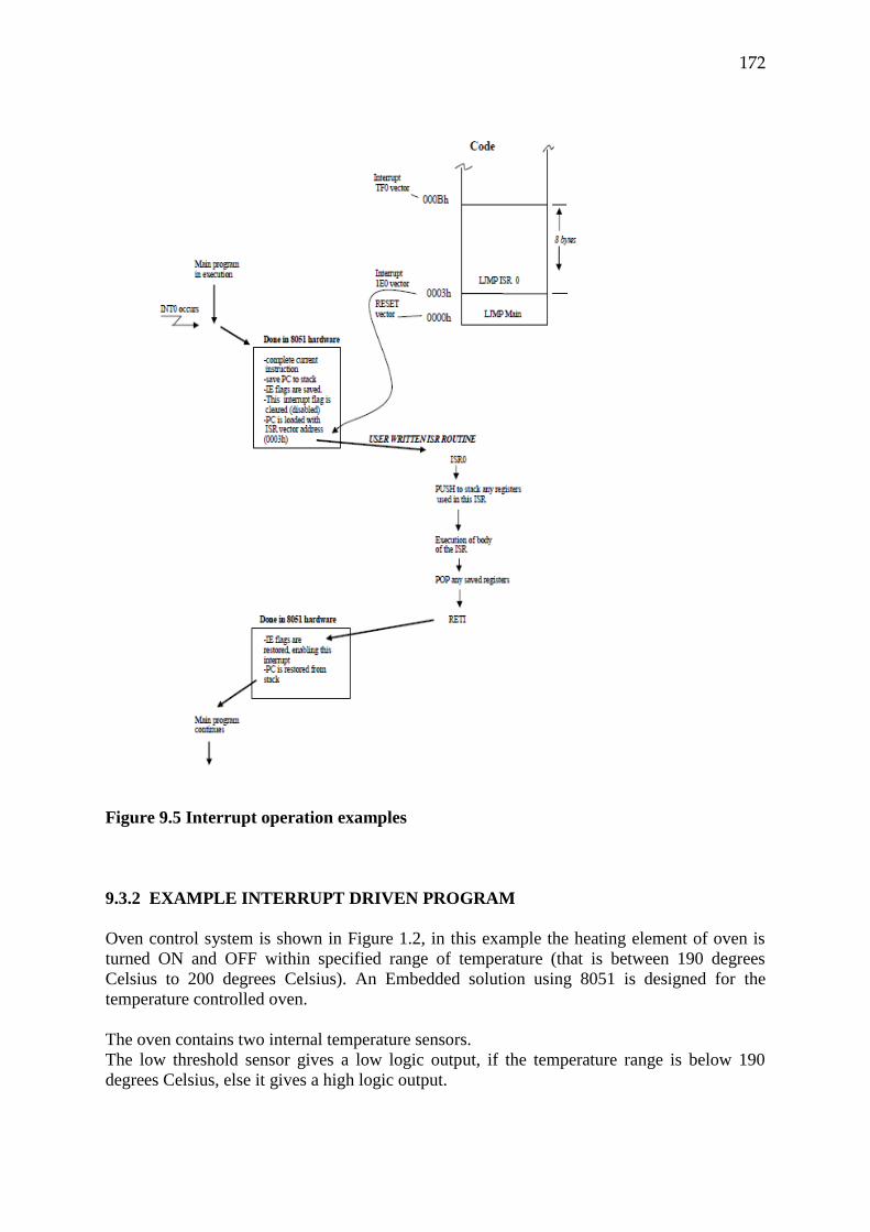
172
Figure 9.5 Interrupt operation examples
9.3.2 EXAMPLE INTERRUPT DRIVEN PROGRAM
Oven control system is shown in Figure 1.2, in this example the heating element of oven is
turned ON and OFF within specified range of temperature (that is between 190 degrees
Celsius to 200 degrees Celsius). An Embedded solution using 8051 is designed for the
temperature controlled oven.
The oven contains two internal temperature sensors.
The low threshold sensor gives a low logic output, if the temperature range is below 190
degrees Celsius, else it gives a high logic output.
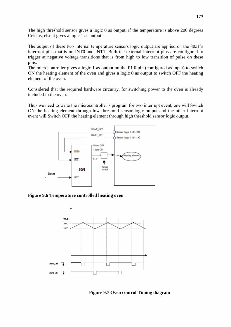
173
The high threshold sensor gives a logic 0 as output, if the temperature is above 200 degrees
Celsius, else it gives a logic 1 as output.
The output of these two internal temperature sensors logic output are applied on the 8051’s
interrupt pins that is on INT0 and INT1. Both the external interrupt pins are configured to
trigger at negative voltage transitions that is from high to low transition of pulse on these
pins.
The microcontroller gives a logic 1 as output on the P1.0 pin (configured as input) to switch
ON the heating element of the oven and gives a logic 0 as output to switch OFF the heating
element of the oven.
Considered that the required hardware circuitry, for switching power to the oven is already
included in the oven.
Thus we need to write the microcontroller’s program for two interrupt event, one will Switch
ON the heating element through low threshold sensor logic output and the other interrupt
event will Switch OFF the heating element through high threshold sensor logic output.
Figure 9.6 Temperature controlled heating oven
Figure 9.7 Oven control Timing diagram
174
The source program in assembly language for controlling the oven is listed in listing.
The ISR routines (Interrupt Service Routines) must be very short so that they can reside
within the 8 bytes of memory available specified at their respective vector locations.
So in the beginning of the given program, three vector locations are defined.
The RESET vector is located at address 0000h and containing a jump instruction for the
MAIN program.
External interrupt (INT0) vector is located at 0003h and containing a jump instruction for its
relevant ISR routine, ISR0.
External interrupt (INT1) vector location address at 0013h and having a jump instruction for
its relevant ISR routine, ISR1.
In the example program for oven control, the loop inside the main program is not doing
anything. Whenever an interrupt event occurs either from INT0 or INT1 the required
execution will be based on their corresponding ISR routine.
When considering a complex program, the loop inside the main program may be busy in
doing some useful work and can be interrupted only when there is need to adjusting (on or
off) the oven temperature. Thus instead of polling the status of sensor, the main program will
do some useful work and saves time.
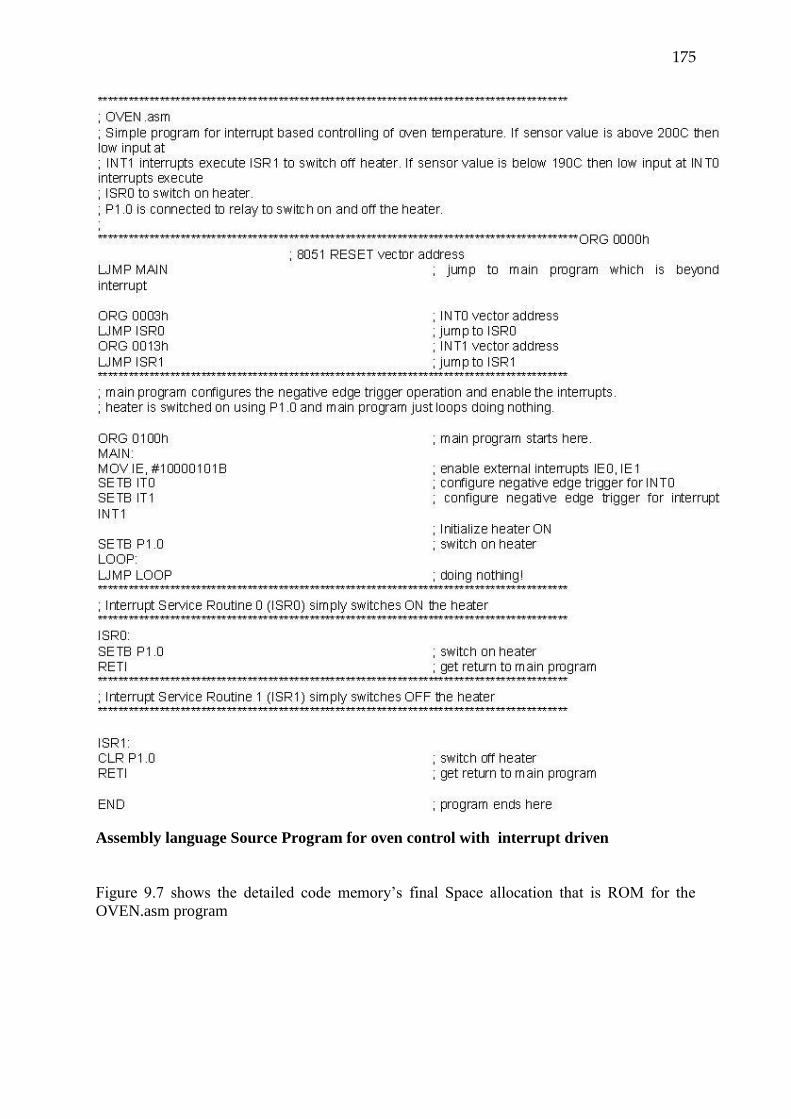
175
Assembly language Source Program for oven control with interrupt driven
Figure 9.7 shows the detailed code memory’s final Space allocation that is ROM for the
OVEN.asm program
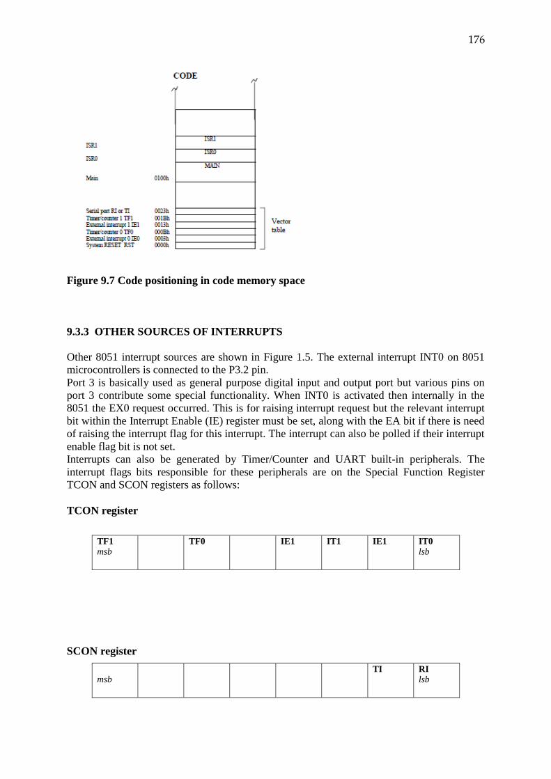
176
Figure 9.7 Code positioning in code memory space
9.3.3 OTHER SOURCES OF INTERRUPTS
Other 8051 interrupt sources are shown in Figure 1.5. The external interrupt INT0 on 8051
microcontrollers is connected to the P3.2 pin.
Port 3 is basically used as general purpose digital input and output port but various pins on
port 3 contribute some special functionality. When INT0 is activated then internally in the
8051 the EX0 request occurred. This is for raising interrupt request but the relevant interrupt
bit within the Interrupt Enable (IE) register must be set, along with the EA bit if there is need
of raising the interrupt flag for this interrupt. The interrupt can also be polled if their interrupt
enable flag bit is not set.
Interrupts can also be generated by Timer/Counter and UART built-in peripherals. The
interrupt flags bits responsible for these peripherals are on the Special Function Register
TCON and SCON registers as follows:
TCON register
SCON register
TF1
msb
TF0 IE1 IT1 IE1 IT0
lsb
msb
TI RI
lsb
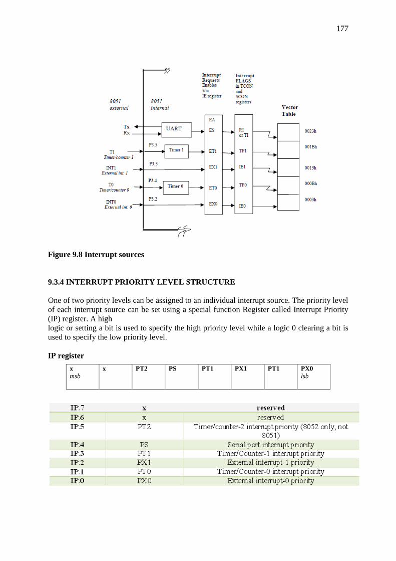
177
Figure 9.8 Interrupt sources
9.3.4 INTERRUPT PRIORITY LEVEL STRUCTURE
One of two priority levels can be assigned to an individual interrupt source. The priority level
of each interrupt source can be set using a special function Register called Interrupt Priority
(IP) register. A high
logic or setting a bit is used to specify the high priority level while a logic 0 clearing a bit is
used to specify the low priority level.
IP register
x
msb
x
PT2 PS PT1 PX1 PT1 PX0
lsb
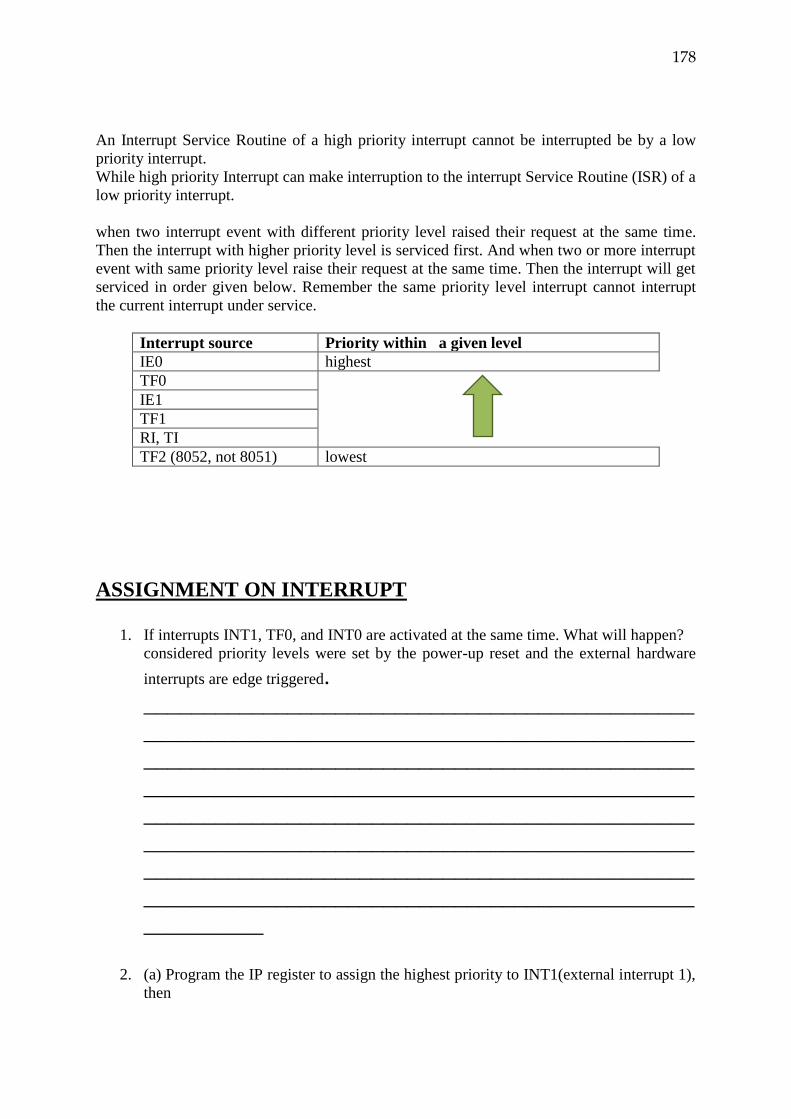
178
An Interrupt Service Routine of a high priority interrupt cannot be interrupted be by a low
priority interrupt.
While high priority Interrupt can make interruption to the interrupt Service Routine (ISR) of a
low priority interrupt.
when two interrupt event with different priority level raised their request at the same time.
Then the interrupt with higher priority level is serviced first. And when two or more interrupt
event with same priority level raise their request at the same time. Then the interrupt will get
serviced in order given below. Remember the same priority level interrupt cannot interrupt
the current interrupt under service.
Interrupt source Priority within a given level
IE0 highest
TF0
IE1
TF1
RI, TI
TF2 (8052, not 8051) lowest
ASSIGNMENT ON INTERRUPT
1. If interrupts INT1, TF0, and INT0 are activated at the same time. What will happen?
considered priority levels were set by the power-up reset and the external hardware
interrupts are edge triggered.
______________________________________________
______________________________________________
______________________________________________
______________________________________________
______________________________________________
______________________________________________
______________________________________________
______________________________________________
__________
2. (a) Program the IP register to assign the highest priority to INT1(external interrupt 1),
then
179
(b) Discuss what happens if INT0, INT1, and TF0 are activated at the same time.
Assume the interrupts are both edge-triggered.
______________________________________________
__
______________________________________________
__
______________________________________________
__
______________________________________________
__
3. Assume that after reset, the interrupt priority is set the instruction MOV IP,
#00001100B. Discuss the sequence in which the interrupts are serviced.
_____________________________________________________________________
_____________________________________________________________________
_____________________________________________________________________
_____________________________________________________________________
____________
Solutions:
1. In case the hree interrupts are activated at the same time, it latched and kept internally.
Then the microcontroller checks these five interrupts according to the sequence. If any
one is activated, it provides service in sequence. So if the above three interrupts are
activated, first, IE0 (external interrupt 0) is serviced, then timer 0 (TF0), and in the last
IE1 (external interrupt 1).
2. (a) MOV IP, #0000100B; IP.2=1 assign INT1 higher priority. The instruction SETB
IP.2 also do the same as the mentioned in above line since IP is bit-addressable.
(b) The higher priority in Step (a) is assigned to INT1 than the others; So if INT0,
INT1, and TF0 interrupts are activated at the same time, the microcontroller
provide service INT1 first and after that services INT0, in last to TF0. It is
because INT1 has a higher priority than the others. In Step (a) both the INT0 and
TF0 bits are presents in the IP register 0. As a result, the sequence in Table below
is followed which gives a higher priority to INT0 over TF0.
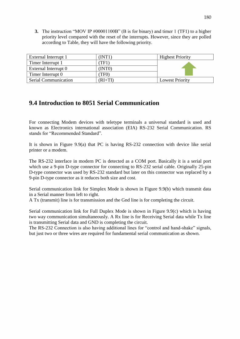
180
3. The instruction “MOV IP #00001100B” (B is for binary) and timer 1 (TF1) to a higher
priority level compared with the reset of the interrupts. However, since they are polled
according to Table, they will have the following priority.
9.4 Introduction to 8051 Serial Communication
For connecting Modem devices with teletype terminals a universal standard is used and
known as Electronics international association (EIA) RS-232 Serial Communication. RS
stands for “Recommended Standard”.
It is shown in Figure 9.9(a) that PC is having RS-232 connection with device like serial
printer or a modem.
The RS-232 interface in modern PC is detected as a COM port. Basically it is a serial port
which use a 9-pin D-type connector for connecting to RS-232 serial cable. Originally 25-pin
D-type connector was used by RS-232 standard but later on this connector was replaced by a
9-pin D-type connector as it reduces both size and cost.
Serial communication link for Simplex Mode is shown in Figure 9.9(b) which transmit data
in a Serial manner from left to right.
A Tx (transmit) line is for transmission and the Gnd line is for completing the circuit.
Serial communication link for Full Duplex Mode is shown in Figure 9.9(c) which is having
two way communication simultaneously. A Rx line is for Receiving Serial data while Tx line
is transmitting Serial data and GND is completing the circuit.
The RS-232 Connection is also having additional lines for “control and hand-shake” signals,
but just two or three wires are required for fundamental serial communication as shown.
External Interrupt 1 (INT1) Highest Priority
Timer Interrupt 1 (TF1)
External Interrupt 0 (INT0)
Timer Interrupt 0 (TF0)
Serial Communication (RI+TI) Lowest Priority
181
Figure 9.9 Serial communications
For transmitting serial data, we need to have predefined transmission rate and that is known
as baud rate. The baud rate can be defined as the number of state changes per second and this
is exactly related to the bit rate for this type of communication. Typical baud rates used for
Serial communication are: 9600 bps; 19,200 bps; 56kbps etc.
Asynchronous Serial Communications
The data is communicated (that is either transmitted or received) in a serial manner, without
any clock pulse which is mainly required for synchronise the receiver and transmitter, thus
the system is known as asynchronous or non-synchronous.
The baud rates for communication at both the end (transmitter and receiver side) must be
equal but these clocks at both end cannot be synchronised.
Three bytes ‘A’,’B’,’C’ transmitted Serially by the PC to Serial Device like Modem or a
Printer is Figure 9.10(a)
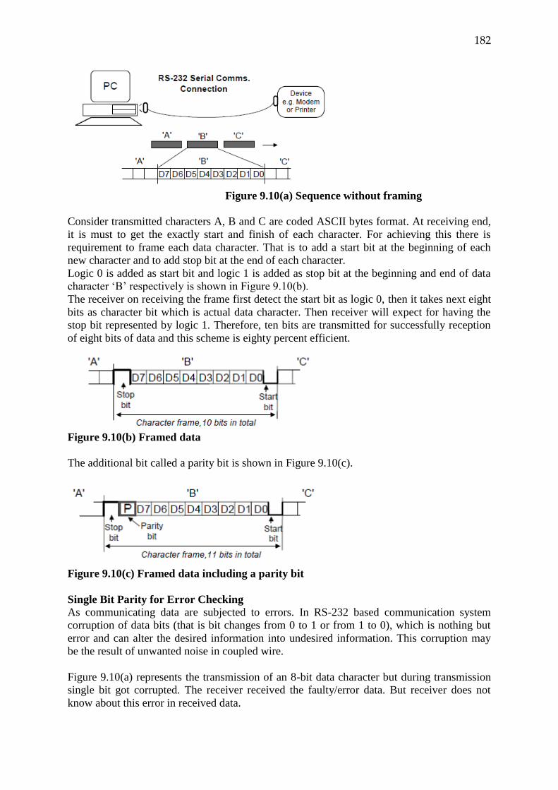
182
Figure 9.10(a) Sequence without framing
Consider transmitted characters A, B and C are coded ASCII bytes format. At receiving end,
it is must to get the exactly start and finish of each character. For achieving this there is
requirement to frame each data character. That is to add a start bit at the beginning of each
new character and to add stop bit at the end of each character.
Logic 0 is added as start bit and logic 1 is added as stop bit at the beginning and end of data
character ‘B’ respectively is shown in Figure 9.10(b).
The receiver on receiving the frame first detect the start bit as logic 0, then it takes next eight
bits as character bit which is actual data character. Then receiver will expect for having the
stop bit represented by logic 1. Therefore, ten bits are transmitted for successfully reception
of eight bits of data and this scheme is eighty percent efficient.
Figure 9.10(b) Framed data
The additional bit called a parity bit is shown in Figure 9.10(c).
Figure 9.10(c) Framed data including a parity bit
Single Bit Parity for Error Checking
As communicating data are subjected to errors. In RS-232 based communication system
corruption of data bits (that is bit changes from 0 to 1 or from 1 to 0), which is nothing but
error and can alter the desired information into undesired information. This corruption may
be the result of unwanted noise in coupled wire.
Figure 9.10(a) represents the transmission of an 8-bit data character but during transmission
single bit got corrupted. The receiver received the faulty/error data. But receiver does not
know about this error in received data.
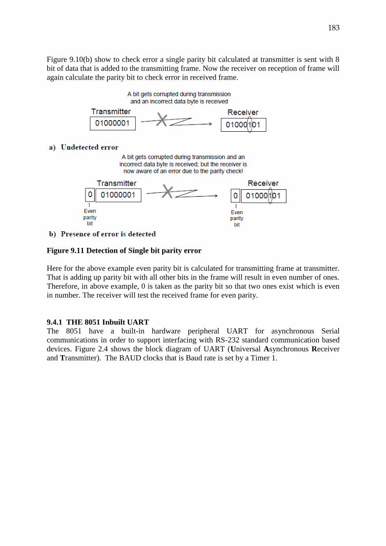
183
Figure 9.10(b) show to check error a single parity bit calculated at transmitter is sent with 8
bit of data that is added to the transmitting frame. Now the receiver on reception of frame will
again calculate the parity bit to check error in received frame.
Figure 9.11 Detection of Single bit parity error
Here for the above example even parity bit is calculated for transmitting frame at transmitter.
That is adding up parity bit with all other bits in the frame will result in even number of ones.
Therefore, in above example, 0 is taken as the parity bit so that two ones exist which is even
in number. The receiver will test the received frame for even parity.
9.4.1 THE 8051 Inbuilt UART
The 8051 have a built-in hardware peripheral UART for asynchronous Serial
communications in order to support interfacing with RS-232 standard communication based
devices. Figure 2.4 shows the block diagram of UART (Universal Asynchronous Receiver
and Transmitter). The BAUD clocks that is Baud rate is set by a Timer 1.
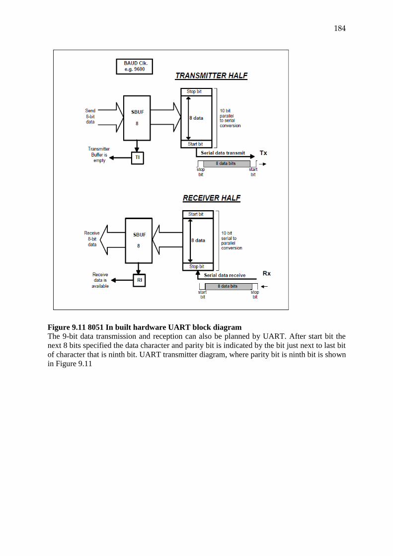
184
Figure 9.11 8051 In built hardware UART block diagram
The 9-bit data transmission and reception can also be planned by UART. After start bit the
next 8 bits specified the data character and parity bit is indicated by the bit just next to last bit
of character that is ninth bit. UART transmitter diagram, where parity bit is ninth bit is shown
in Figure 9.11
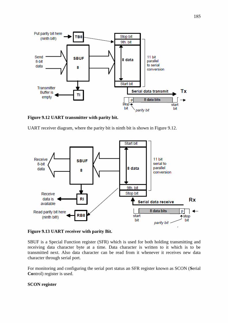
185
Figure 9.12 UART transmitter with parity bit.
UART receiver diagram, where the parity bit is ninth bit is shown in Figure 9.12.
Figure 9.13 UART receiver with parity Bit.
SBUF is a Special Function register (SFR) which is used for both holding transmitting and
receiving data character byte at a time. Data character is written to it which is to be
transmitted next. Also data character can be read from it whenever it receives new data
character through serial port.
For monitoring and configuring the serial port status an SFR register known as SCON (Serial
Control) register is used.
SCON register
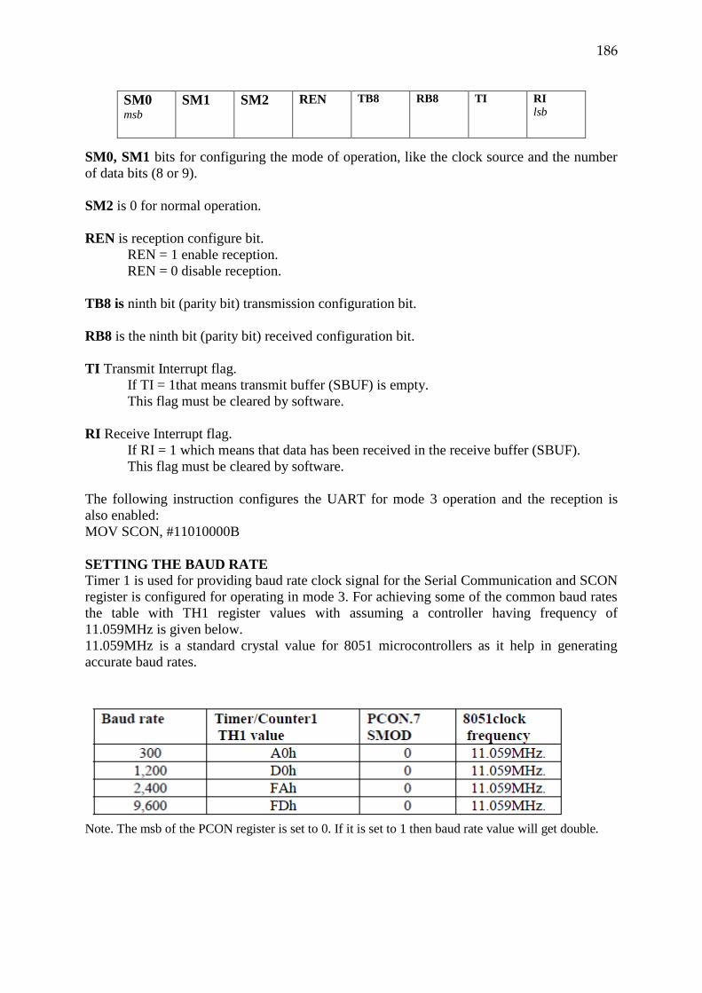
186
SM0, SM1 bits for configuring the mode of operation, like the clock source and the number
of data bits (8 or 9).
SM2 is 0 for normal operation.
REN is reception configure bit.
REN = 1 enable reception.
REN = 0 disable reception.
TB8 is ninth bit (parity bit) transmission configuration bit.
RB8 is the ninth bit (parity bit) received configuration bit.
TI Transmit Interrupt flag.
If TI = 1that means transmit buffer (SBUF) is empty.
This flag must be cleared by software.
RI Receive Interrupt flag.
If RI = 1 which means that data has been received in the receive buffer (SBUF).
This flag must be cleared by software.
The following instruction configures the UART for mode 3 operation and the reception is
also enabled:
MOV SCON, #11010000B
SETTING THE BAUD RATE
Timer 1 is used for providing baud rate clock signal for the Serial Communication and SCON
register is configured for operating in mode 3. For achieving some of the common baud rates
the table with TH1 register values with assuming a controller having frequency of
11.059MHz is given below.
11.059MHz is a standard crystal value for 8051 microcontrollers as it help in generating
accurate baud rates.
Note. The msb of the PCON register is set to 0. If it is set to 1 then baud rate value will get double.
SM0 msb
SM1 SM2 REN TB8 RB8 TI RI
lsb
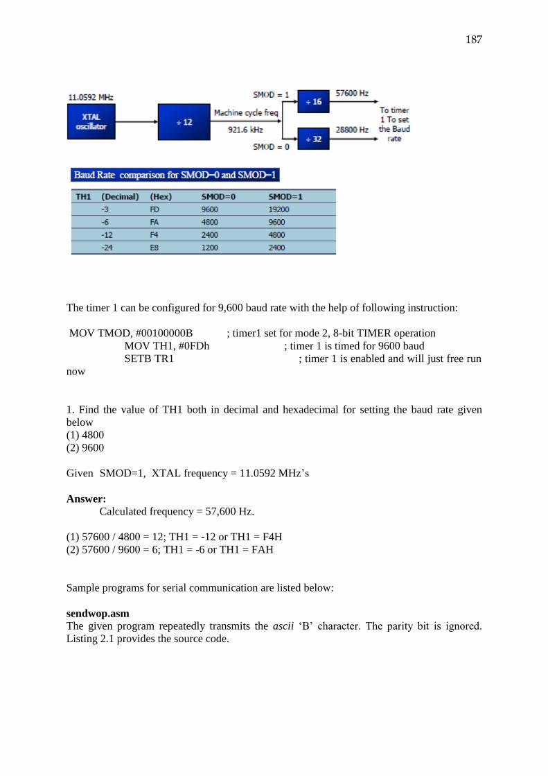
187
The timer 1 can be configured for 9,600 baud rate with the help of following instruction:
MOV TMOD, #00100000B ; timer1 set for mode 2, 8-bit TIMER operation
MOV TH1, #0FDh ; timer 1 is timed for 9600 baud
SETB TR1 ; timer 1 is enabled and will just free run
now
1. Find the value of TH1 both in decimal and hexadecimal for setting the baud rate given
below
(1) 4800
(2) 9600
Given SMOD=1, XTAL frequency = 11.0592 MHz’s
Answer:
Calculated frequency = 57,600 Hz.
(1) 57600 / 4800 = 12; TH1 = -12 or TH1 = F4H
(2) 57600 / 9600 = 6; TH1 = -6 or TH1 = FAH
Sample programs for serial communication are listed below:
sendwop.asm
The given program repeatedly transmits the ascii ‘B’ character. The parity bit is ignored.
Listing 2.1 provides the source code.
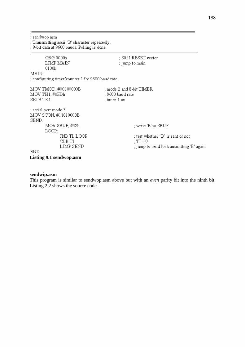
188
Listing 9.1 sendwop.asm
sendwip.asm
This program is similar to sendwop.asm above but with an even parity bit into the ninth bit.
Listing 2.2 shows the source code.
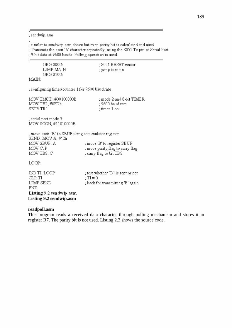
189
Listing 9.2 sendwip.asm
readpoll.asm
This program reads a received data character through polling mechanism and stores it in
register R7. The parity bit is not used. Listing 2.3 shows the source code.
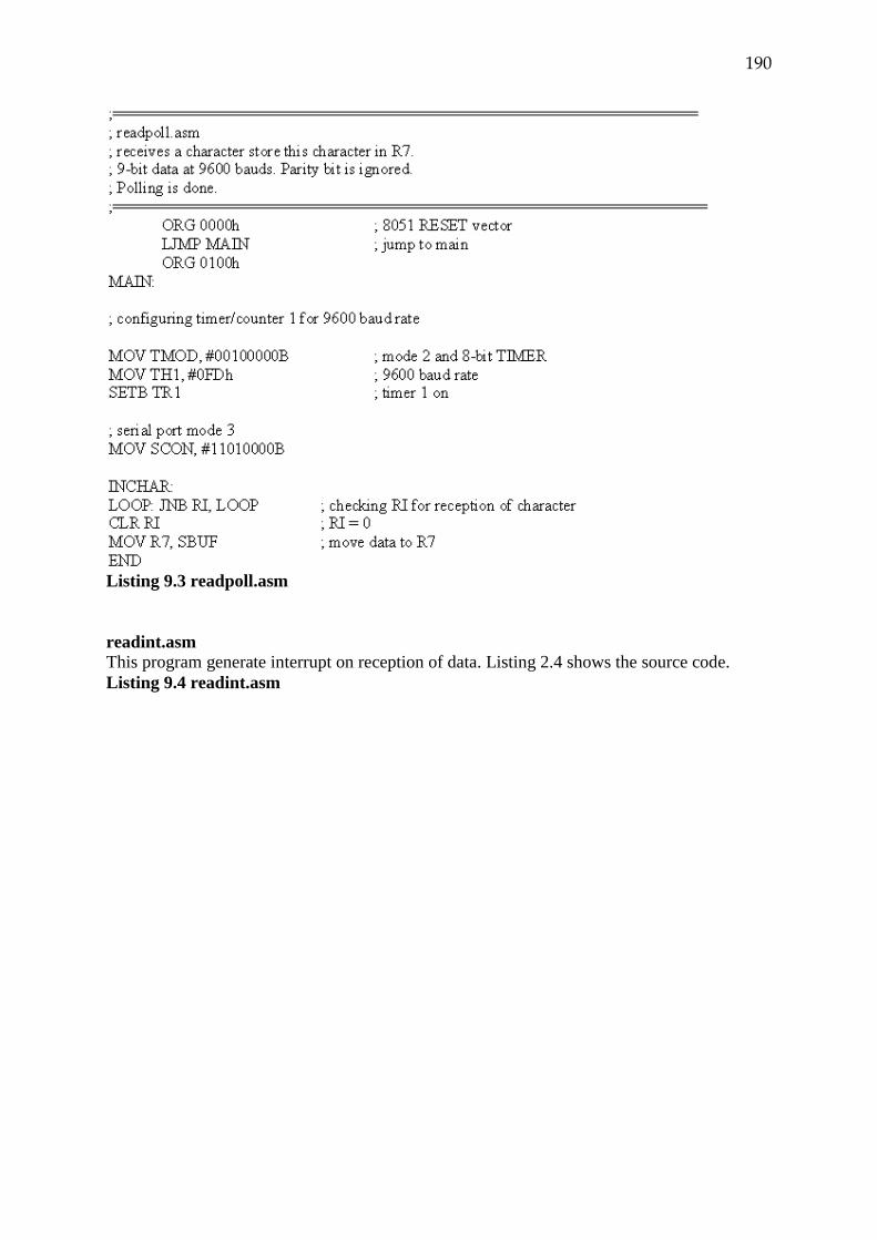
190
Listing 9.3 readpoll.asm
readint.asm
This program generate interrupt on reception of data. Listing 2.4 shows the source code.
Listing 9.4 readint.asm
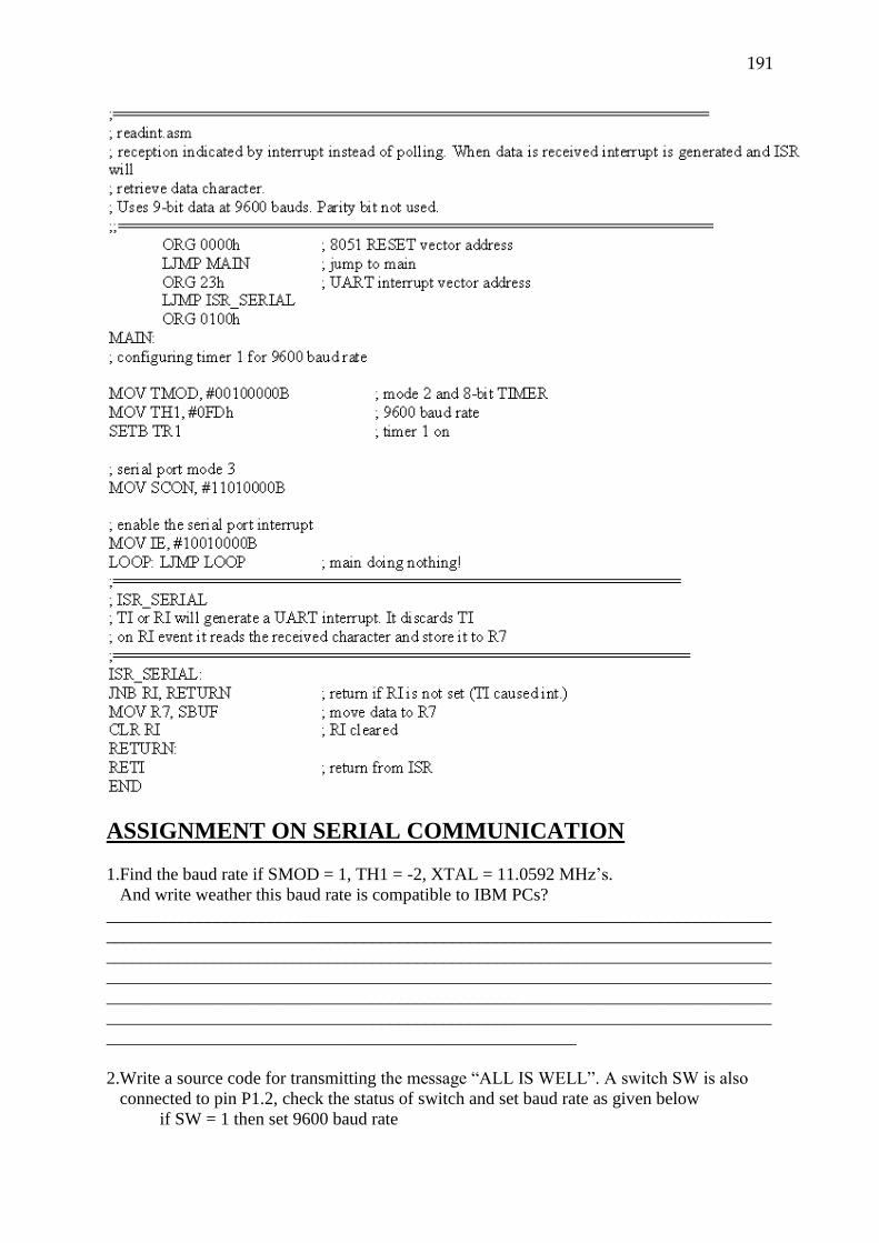
191
ASSIGNMENT ON SERIAL COMMUNICATION
1.Find the baud rate if SMOD = 1, TH1 = -2, XTAL = 11.0592 MHz’s.
And write weather this baud rate is compatible to IBM PCs?
___________________________________________________________________________
___________________________________________________________________________
___________________________________________________________________________
___________________________________________________________________________
___________________________________________________________________________
___________________________________________________________________________
_____________________________________________________
2.Write a source code for transmitting the message “ALL IS WELL”. A switch SW is also
connected to pin P1.2, check the status of switch and set baud rate as given below
if SW = 1 then set 9600 baud rate
192
if SW = 0 then set 4800 baud rate
Given 8-bit data, XTAL = 11.0592 MHz, 1 stop bit.
___________________________________________________________________________
___________________________________________________________________________
___________________________________________________________________________
___________________________________________________________________________
___________________________________________________________________________
___________________________________________________________________________
___________________________________________________________________________
___________________________________________________________________________
___________________________________________________________________________
___________________________________________________________________________
___________________________________________________________________________
___________________________________________________________________________
___________________________________________________________________________
___________________________________________________________________________
___________________________________________________________________________
___________________________________________________________________________
___________________________________________________________________________
______________________________
3.Given the frequency of XTAL = 11.0592 MHz for the below program,
state (a) what the given code will do
(b) calculate the frequency used by timer 1
(c) also calculate the baud rate.
Solutions:
Solution 1:
With XTAL = 11.0592 and SMOD = 1, we have timer frequency = 57,600 Hz. The baud rate
is 57,600/2 = 28,800.
193
BIOS of the PCs will not support this baud rate; however the PC can be programmed to do
data transfer at such a speed. But HyperTerminal in Windows supports this as well as other
baud rates.
Solution 2:
Solution 3:
(1) This program will transmit ASCII letter A (01000010 binary) continuously
(2) as given XTAL = 11.0592 MHz and SMOD = 1
Frequency used by timer 1 can be calculated as
11.0592 / 12 = 921.6 kHz.
921.6 / 16 = 57,600 Hz frequency used by timer 1to set the
baud rate.
The baud rate is given by
57600 / 3 = 19,200.
194
Chapter 10
Introduction to DMA Controller 8257 Architecture ___________________________________________________________________________
___________________________________________________________________________
Structure
10.0 Objectives
10.1 Introduction
10.2 Intel 8257 DMA Controller
10.3 Mode of Operation of DMA Controller
10.4 Block Diagram and Pin Description of Intel 8257 DMA Controller
10.5 8257 Operation
1.5.1 Programming and Reading the 8257 Registers
1.5.2 Operational Description
10.6 Answer to Check Your Progress/Suggested Answers to SAQ
10.7 Bibliography/References/ Suggested Readings
10.8 Terminal and Model Questions
10.0 Objectives
After studying this chapter you will understand
Block Diagram and Pin Description of Intel 8257 DMA Controller.
Mode of Operation of DMA Controller
8257 Operations.
195
10.1 Introduction
The Direct Memory Access (DMA) is a process of high speed direct data transfer. DMA is
generally used data transfer between memory and external peripherals I/O device, without
involving the CPU. where microprocessor controlled data transfer is too slow. E.g. - Data
transfer between a floppy disk and R/W memory of the system. A DMA Controller
(8257/8237 ICs) is used for interface the peripheral of the system. The DMA Controller takes
control on the buses and transfer data directly between memory and external peripherals.
When large amount of data is to be transferred from memory of the computer to an external
device than DMA is useful because it avoids the use of CPU and allows the CPU to attain
another job.
The 8085 microprocessor has two types of signals for direct memory access.
HOLD (Hold request) –Hold is an active high input signal of the 8085. This signal is high,
than master is requesting to use the address and data buses. If HOLD request is obtained than
microprocessor unit (MPU) connects the buses in the following machine cycle. In this case,
HLDA signal is sent out by all buses. This process is continue unless HOLD request will go
low and after that MPU regains the control of buses.
HLDA (Hold Acknowledge) – HLDA is an active high output signal, which shows that the
MPU is releasing the control of the buses.
DMA Controller sends a hold request by sending high signal on HOLD pin of 8085. The
Processor completes the execution of current machine cycle and send the HLDA (Hold
acknowledge) signal. These signals are used by DMA Controller, if peripheral requesting the
MPU for the control of the buses. Chip select line, buses and control signals are used for
communication between MPU and Controller. For data transfer, the DMA controller should
have a data bus, an address bus, read/write control signal and a control signal for disable and
enable the roll of peripheral and processor. The programmer DMA Controller, 8257 is
explained below.
10.2 Intel 8257 DMA Controller
Intel 8257 DMA Controller has four channels so it can be used to provide DMA to four I/O
devices, each channel can be independently programmable to transfer up to 64k bytes of data.
Each channel has two 16 bit registers, those are address register and a terminal count register.
If peripherals connected to the channel send a DMA request then 8257 hold the control of the
system bus and send an acknowledge to the peripheral. DMA controller also generates
control signal for the memory or I/O read or write operation and transfer data in a single
burst. 8257 DMA Controller informs the CPU that operation is completed by activating its
terminal count output.
10.3 Mode of Operation of DMA Controller
There are three modes of operation of 8257 DMA Controller-
DMA read
DMA write
DMA verify
1) DMA Write Mode - when data is to be transferred from a high speed peripheral to main
memory.
196
2) DMA Read Mode - when data is to be transferred from main memory to a high speed
peripheral.
3) DMA Verify Mode - when data is not transferred between a high speed peripheral and
main memory. The 8257 DMA Controller holds the control of the system bus and
acknowledges the peripheral. This generated acknowledges signals can be used by the
peripheral to verify the acquired data.
10.4 Block Diagram and Pin Description of Intel 8257 DMA Controller
Block diagram of Intel 8257 is shown in Figure 1. DMA controller functional block diagram
has
DMA Channels
Read/Write Logic
Data Bus Buffer
Control Logic, Mode Set Register and Status Register.
1. DMA Channels
DMA Controller has four isolated DMA channels (CH0-CH3) and each channel has a 16-bit
terminal count (TC) register and a 16-bit DMA address register. Before channel enabling
both registers (Terminal count and address) must be initialized before.
DMA Address Register: It is used to store initial memory location address to be
accessed.
DMA Terminal Count Register: It is used to store the number of bytes to be
accessed. The count value represents the number of DMA cycles required to
activate the Terminal Count (TC) output and count value is stored into the lower
14-bits (0 to 13) of the terminal count register. For example if n represents the
number of required DMA cycles, then n-1 will be loaded in the lower 14-bits (0 to
13) of the terminal count register. The most significant two bits (Bit 15 and 14) of
the terminal count register are used to set the operating mode of the channel.
Table 1: DMA mode of operation using terminal count register bit 16 and 15
Bit 15 Bit 14 DMA operation
0 0 Verify DMA cycle
0 1 Read DMA cycle
1 0 Write DMA cycle
1 1 Illegal
Each DMA channel has a DMA Request (DRQ) input and a DMA Acknowledge (DACK)
output. In response of DMA Request (DRQ) it provide a DMA Acknowledge (DACK).
DRQ 0 - DRQ 3
DMA Request: To obtain a DMA cycle four individual asynchronous input signals are used
by the peripherals and send a request by raising the DRQ input high and keep it high until
DMA send a acknowledge signal. In the case of multiple DMA cycles the DRQ line is held
high until the DMA acknowledge of the last cycle arrives. If the two or more request come
simultaneously then highest priority is given to DRQ 0 and lowest to DRQ 3.
197
𝐃𝐀𝐂𝐊 𝟎 − 𝐃𝐀𝐂𝐊 𝟑
DMA Acknowledge: These are active low output lines connected to channel. These lines are
used to provide acknowledgement in response to the peripheral request. After serving the
request DACK output is moved to high.
2. Data Bus Buffer
It is used to interface internal bus of DMA controller to the 8 bit external bus of
microprocessor.
It works as a tristate bidirectional buffer under the control of read write logic block signals.
Data bus lines (D0-D7):
In “slave mode”: Data bus lines are used as input pins and CPU has control over the system
bus. 8 bits data, of 8 bit mode set register or 16 bit DMA address register or 16 bit terminal
count register, can be received at a time through these data bits lines.
In “Master mode”: Data bus lines are used as a master bus. The 8257 sent the most significant
eight-bits of one DMA address registers to the 8212 latch via the data bus as a memory
address at start of the DMA cycle. Then bus can be used to memory data transfer.
3. Read/Write Logic
In the “slave mode” (I/O to the microprocessor), the I/O Read, I/O Write and A0-A7 pins of
the 8257 are used as input pins.
In case of “master mode” (data transfer processor to peripherals), the A0-A7 bits are used as
output pins.
𝑰/𝑶𝑹
I/O Read: It is a bi-directional three-state active low line and used as an input in slave mode
and as an output in master mode. In slave mode it allows the data to be read from the
upper/lower byte of a 16-bit terminal count register or DMA address register or into the mode
set register. In master mode this is used to read data during the DMA write cycle from a
peripheral.
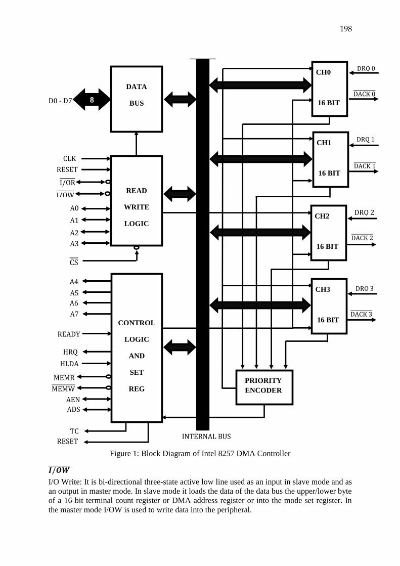
198
Figure 1: Block Diagram of Intel 8257 DMA Controller
𝑰/𝑶𝑾
I/O Write: It is bi-directional three-state active low line used as an input in slave mode and as
an output in master mode. In slave mode it loads the data of the data bus the upper/lower byte
of a 16-bit terminal count register or DMA address register or into the mode set register. In
the master mode I/OW is used to write data into the peripheral.
DRQ 0
DACK 0
DRQ 1
DACK 1
DRQ 2
DACK 2
INTERNAL BUS RESET
TC
ADS
TB
AEN
MEMW
MEMR
HLDA
HRQ
READY
A7
A6
A5
A4
CS
A3
A2
A1
A0
I/OW
I/OR
RESET
CLK
8
DATA
BUS
BUFFER
READ
WRITE
LOGIC
CONTROL
LOGIC
AND
SET
REG
CH0
16 BIT
ADDR
CNTR
CH1
16 BIT
ADDR
CNTR
CH2
16 BIT
ADDR
CNTR
CH3
16 BIT
ADDR
CNTR
PRIORITY
ENCODER
D0 - D7
DACK 3
DRQ 3
199
(A0-A7)
Address Lines: Lower four address lines (A0-A3) are bi-directional and remaining address
lines (A4-A7) are unidirectional output. In slave mode address lines (A0-A3) are used to
select register to be read or write. In master mode Lower four address lines (A0-A3) are used
as outputs pins which hold the lower four bits of DMA controller generated 16-bit memory
address.
(𝑪𝑺 )
Chip Select: This is an active-low input.
In slave mode: Chip select input enables the I/O Write or I/O Read input.
In master mode: Chip select input disabled automatically to prevent the chip from selecting
itself.
(RESET)
Reset: This is an asynchronous active high input. This input is generally connected to 8085A
or an external clock generator (8224).It clears the mode set register to disable all DMA
channels and all 3-states control lines.
(CLK)
CLK Input: This input is generally connected to 8085A CLK output or an external clock
generator (8224).
4. Control Logics
Control logics are used to control the sequence of operations by generating the appropriate
control signals, and the 16-bit address that specifies the memory location to be accessed.
(A4-A7)
These are four three- state output address lines. These most significant bits of DMA address
register are used by the 8257 in case of all DMA cycle.
(READY)
This is an asynchronous input used to insert wait states, when peripheral is not ready to data
transfer. HIGH READY signal indicates that slower peripheral (I/O or memory) is ready to
communicate and LOW READY signal insert a wait state in read and write cycles.
(HRQ)
Hold Request (HRQ) is an output pin. With the help of this pin 8257 requests for the control
of the system buses. If the system have only one 8257 then HRQ will be applied to the
HOLD input on the CPU.
(HLDA)
Hold Acknowledge (HLDA) is an input pin. This input pin of 8257 is connected to the
HLDA output pin of 8085. HIGH value of HLDA input indicates that the 8257 has acquired
control of the system bus.
(MEMW)
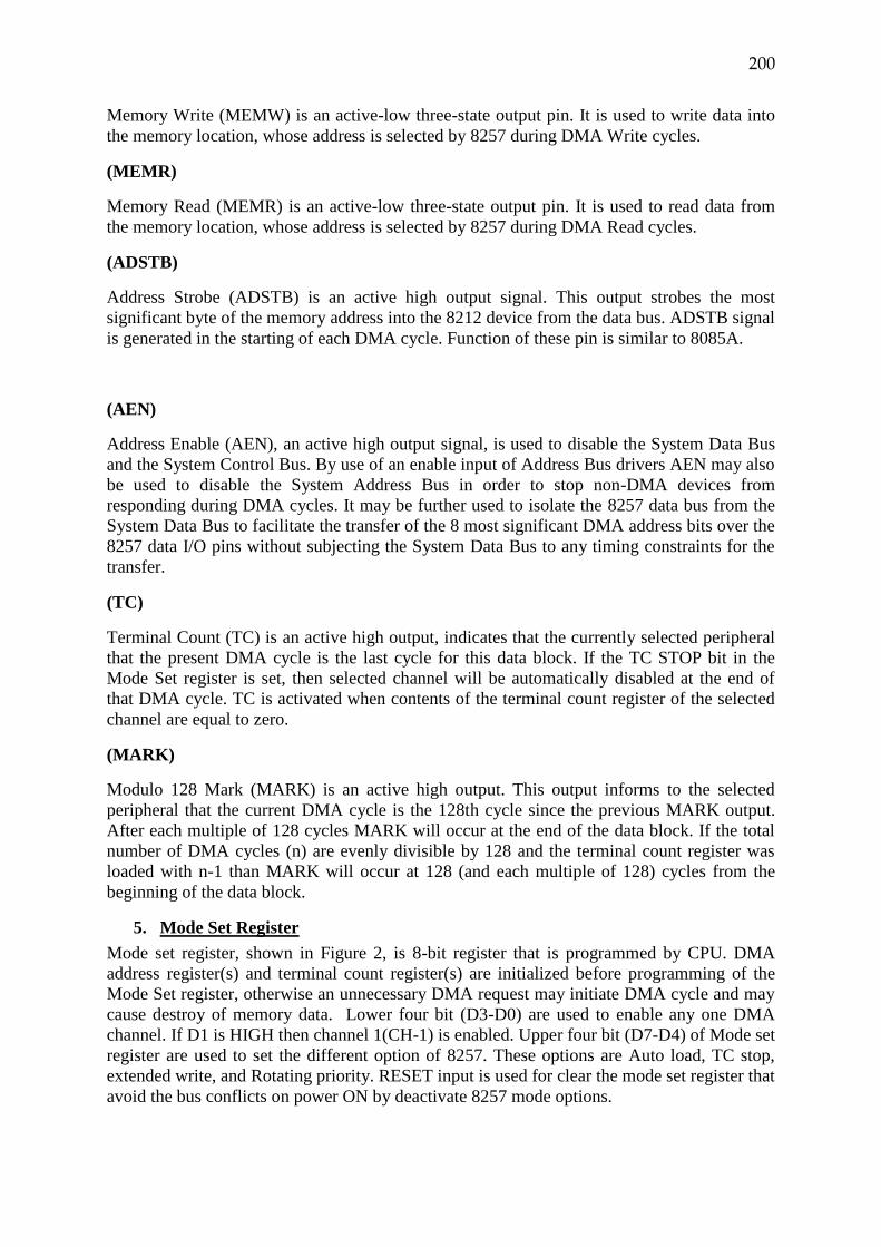
200
Memory Write (MEMW) is an active-low three-state output pin. It is used to write data into
the memory location, whose address is selected by 8257 during DMA Write cycles.
(MEMR)
Memory Read (MEMR) is an active-low three-state output pin. It is used to read data from
the memory location, whose address is selected by 8257 during DMA Read cycles.
(ADSTB)
Address Strobe (ADSTB) is an active high output signal. This output strobes the most
significant byte of the memory address into the 8212 device from the data bus. ADSTB signal
is generated in the starting of each DMA cycle. Function of these pin is similar to 8085A.
(AEN)
Address Enable (AEN), an active high output signal, is used to disable the System Data Bus
and the System Control Bus. By use of an enable input of Address Bus drivers AEN may also
be used to disable the System Address Bus in order to stop non-DMA devices from
responding during DMA cycles. It may be further used to isolate the 8257 data bus from the
System Data Bus to facilitate the transfer of the 8 most significant DMA address bits over the
8257 data I/O pins without subjecting the System Data Bus to any timing constraints for the
transfer.
(TC)
Terminal Count (TC) is an active high output, indicates that the currently selected peripheral
that the present DMA cycle is the last cycle for this data block. If the TC STOP bit in the
Mode Set register is set, then selected channel will be automatically disabled at the end of
that DMA cycle. TC is activated when contents of the terminal count register of the selected
channel are equal to zero.
(MARK)
Modulo 128 Mark (MARK) is an active high output. This output informs to the selected
peripheral that the current DMA cycle is the 128th cycle since the previous MARK output.
After each multiple of 128 cycles MARK will occur at the end of the data block. If the total
number of DMA cycles (n) are evenly divisible by 128 and the terminal count register was
loaded with n-1 than MARK will occur at 128 (and each multiple of 128) cycles from the
beginning of the data block.
5. Mode Set Register
Mode set register, shown in Figure 2, is 8-bit register that is programmed by CPU. DMA
address register(s) and terminal count register(s) are initialized before programming of the
Mode Set register, otherwise an unnecessary DMA request may initiate DMA cycle and may
cause destroy of memory data. Lower four bit (D3-D0) are used to enable any one DMA
channel. If D1 is HIGH then channel 1(CH-1) is enabled. Upper four bit (D7-D4) of Mode set
register are used to set the different option of 8257. These options are Auto load, TC stop,
extended write, and Rotating priority. RESET input is used for clear the mode set register that
avoid the bus conflicts on power ON by deactivate 8257 mode options.
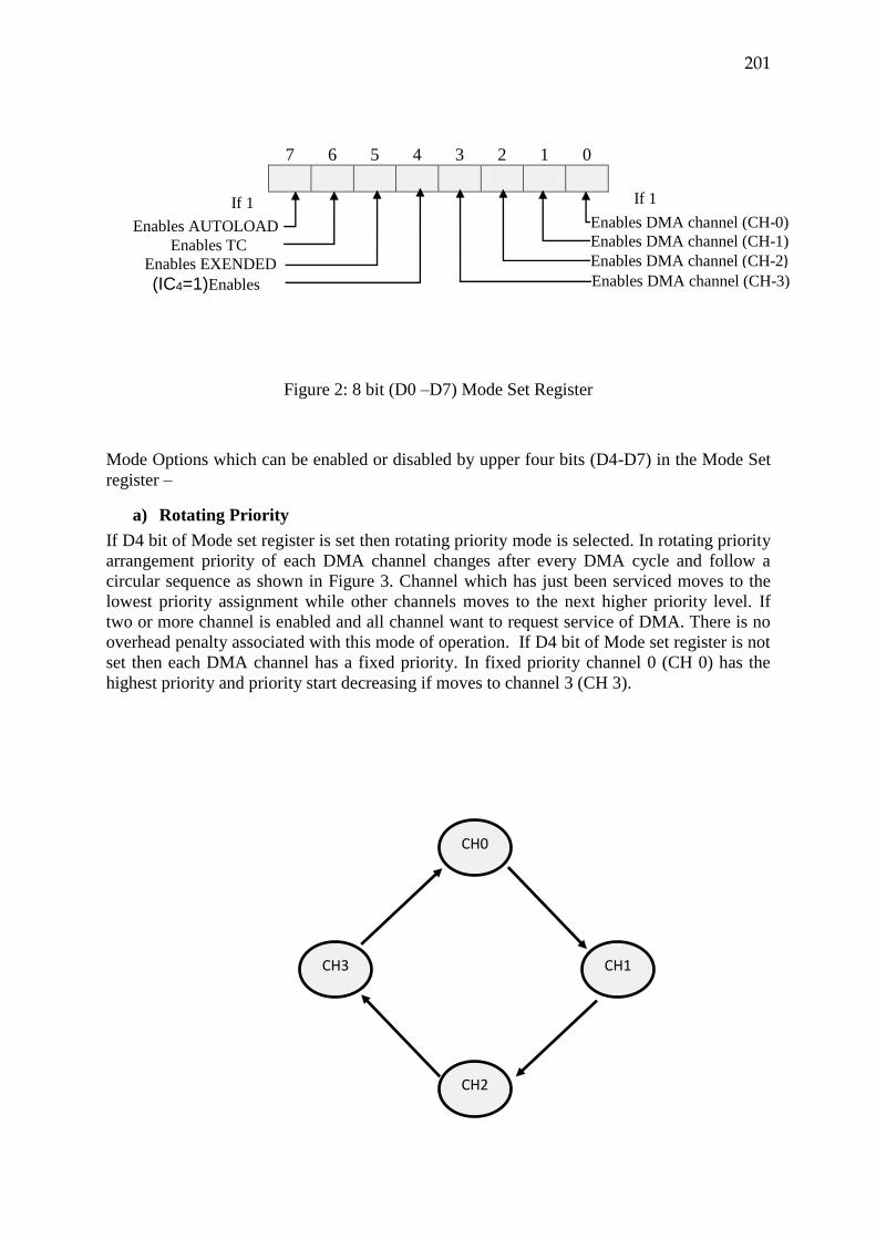
201
7 6 5 4 3 2 1 0
Figure 2: 8 bit (D0 –D7) Mode Set Register
Mode Options which can be enabled or disabled by upper four bits (D4-D7) in the Mode Set
register –
a) Rotating Priority
If D4 bit of Mode set register is set then rotating priority mode is selected. In rotating priority
arrangement priority of each DMA channel changes after every DMA cycle and follow a
circular sequence as shown in Figure 3. Channel which has just been serviced moves to the
lowest priority assignment while other channels moves to the next higher priority level. If
two or more channel is enabled and all channel want to request service of DMA. There is no
overhead penalty associated with this mode of operation. If D4 bit of Mode set register is not
set then each DMA channel has a fixed priority. In fixed priority channel 0 (CH 0) has the
highest priority and priority start decreasing if moves to channel 3 (CH 3).
CH0
CH1 CH3
CH2
(IC4=1)Enables
ROTATING
PRIORITY
If 1 If 1
Enables DMA channel (CH-0)
Enables DMA channel (CH-1)
Enables DMA channel (CH-2) Enables DMA channel (CH-3)
Enables AUTOLOAD
Enables EXENDED
WRITE
Enables TC
STOP
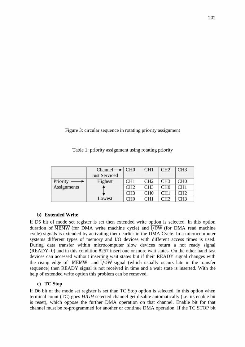
202
Figure 3: circular sequence in rotating priority assignment
Table 1: priority assignment using rotating priority
Channel
Just Serviced
CH0 CH1 CH2 CH3
Priority
Assignments
Highest
Lowest
CH1 CH2 CH3 CH0
CH2 CH3 CH0 CH1
CH3 CH0 CH1 CH2
CH0 CH1 CH2 CH3
b) Extended Write
If D5 bit of mode set register is set then extended write option is selected. In this option
duration of MEMW (for DMA write machine cycle) and I/OW (for DMA read machine
cycle) signals is extended by activating them earlier in the DMA Cycle. In a microcomputer
systems different types of memory and I/O devices with different access times is used.
During data transfer within microcomputer slow devices return a not ready signal
(READY=0) and in this condition 8257 insert one or more wait states. On the other hand fast
devices can accessed without inserting wait states but if their READY signal changes with
the rising edge of MEMW and I/OW signal (which usually occurs late in the transfer
sequence) then READY signal is not received in time and a wait state is inserted. With the
help of extended write option this problem can be removed.
c) TC Stop
If D6 bit of the mode set register is set than TC Stop option is selected. In this option when
terminal count (TC) goes HIGH selected channel get disable automatically (i.e. its enable bit
is reset), which oppose the further DMA operation on that channel. Enable bit for that
channel must be re-programmed for another or continue DMA operation. If the TC STOP bit
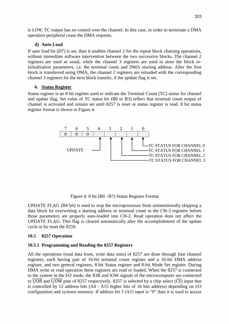
203
is LOW, TC output has no control over the channel. In this case, in order to terminate a DMA
operation peripheral cease the DMA requests.
d) Auto Load
If auto load bit (D7) is set, then it enables channel 2 for the repeat block chaining operations,
without immediate software intervention between the two successive blocks. The channel 2
registers are used as usual, while the channel 3 registers are used to store the block re-
initialization parameters, i.e. the terminal count and DMA starting address. After the first
block is transferred using DMA, the channel 2 registers are reloaded with the corresponding
channel 3 registers for the next block transfer, if the update flag is set.
6. Status Register
Status register is an 8 bit register used to indicate the Terminal Count (TC) status for channel
and update flag. Set value of TC status bit (B0 to B3) reflect that terminal count output of
channel is activated and remain set until 8257 is reset or status register is read. 8 bit status
register format is shown in Figure 4.
7 6 5 4 3 2 1 0
0 0 0
Figure 4: 8 bit (B0 –B7) Status Register Format
UPDATE FLAG (B4 bit) is used to stop the microprocessor from unintentionally skipping a
data block by overwriting a starting address or terminal count in the CH-3 registers before
those parameters are properly auto-loaded into CH-2. Read operation does not affect the
UPDATE FLAG. This flag is cleared automatically after the accomplishment of the update
cycle or by reset the 8259.
10.5 8257 Operation
10.5.1 Programming and Reading the 8257 Registers
All the operations (read data from, write data onto) of 8257 are done through four channel
registers, each having pair of 16-bit terminal count register and a 16-bit DMA address
register, and two general registers, 8-bit Status register and 8-bit Mode Set register. During
DMA write or read operation these registers are read or loaded. When the 8257 is connected
to the system in the I/O mode, the IOR and IOW signals of the microcomputer are connected
to I/OR and I/OW pins of 8257 respectively. 8257 is selected by a chip select (CS ) input that
is controlled by 12 address bits (A4 - A15 higher bits of 16 bits address) depending on I/O
configuration and systems memory. If address bit 3 (A3) input is “0” than it is used to access
UPDATE
FLAG
TC STATUS FOR CHANNEL 0
TC STATUS FOR CHANNEL 1
TC STATUS FOR CHANNEL 2 TC STATUS FOR CHANNEL 3
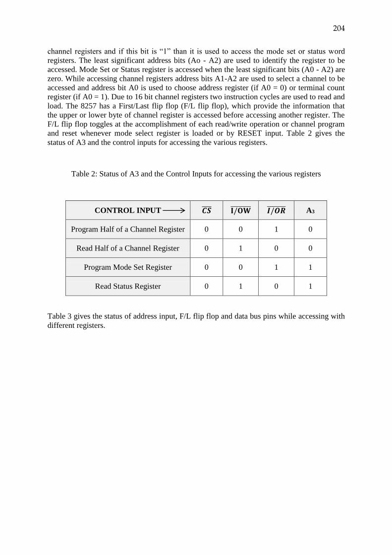
204
channel registers and if this bit is “1” than it is used to access the mode set or status word
registers. The least significant address bits (Ao - A2) are used to identify the register to be
accessed. Mode Set or Status register is accessed when the least significant bits (A0 - A2) are
zero. While accessing channel registers address bits A1-A2 are used to select a channel to be
accessed and address bit A0 is used to choose address register (if A0 = 0) or terminal count
register (if A0 = 1). Due to 16 bit channel registers two instruction cycles are used to read and
load. The 8257 has a First/Last flip flop (F/L flip flop), which provide the information that
the upper or lower byte of channel register is accessed before accessing another register. The
F/L flip flop toggles at the accomplishment of each read/write operation or channel program
and reset whenever mode select register is loaded or by RESET input. Table 2 gives the
status of A3 and the control inputs for accessing the various registers.
Table 2: Status of A3 and the Control Inputs for accessing the various registers
CONTROL INPUT 𝑪𝑺 𝐈/𝐎𝐖 𝑰/𝑶𝑹 A3
Program Half of a Channel Register 0 0 1 0
Read Half of a Channel Register 0 1 0 0
Program Mode Set Register 0 0 1 1
Read Status Register 0 1 0 1
Table 3 gives the status of address input, F/L flip flop and data bus pins while accessing with
different registers.
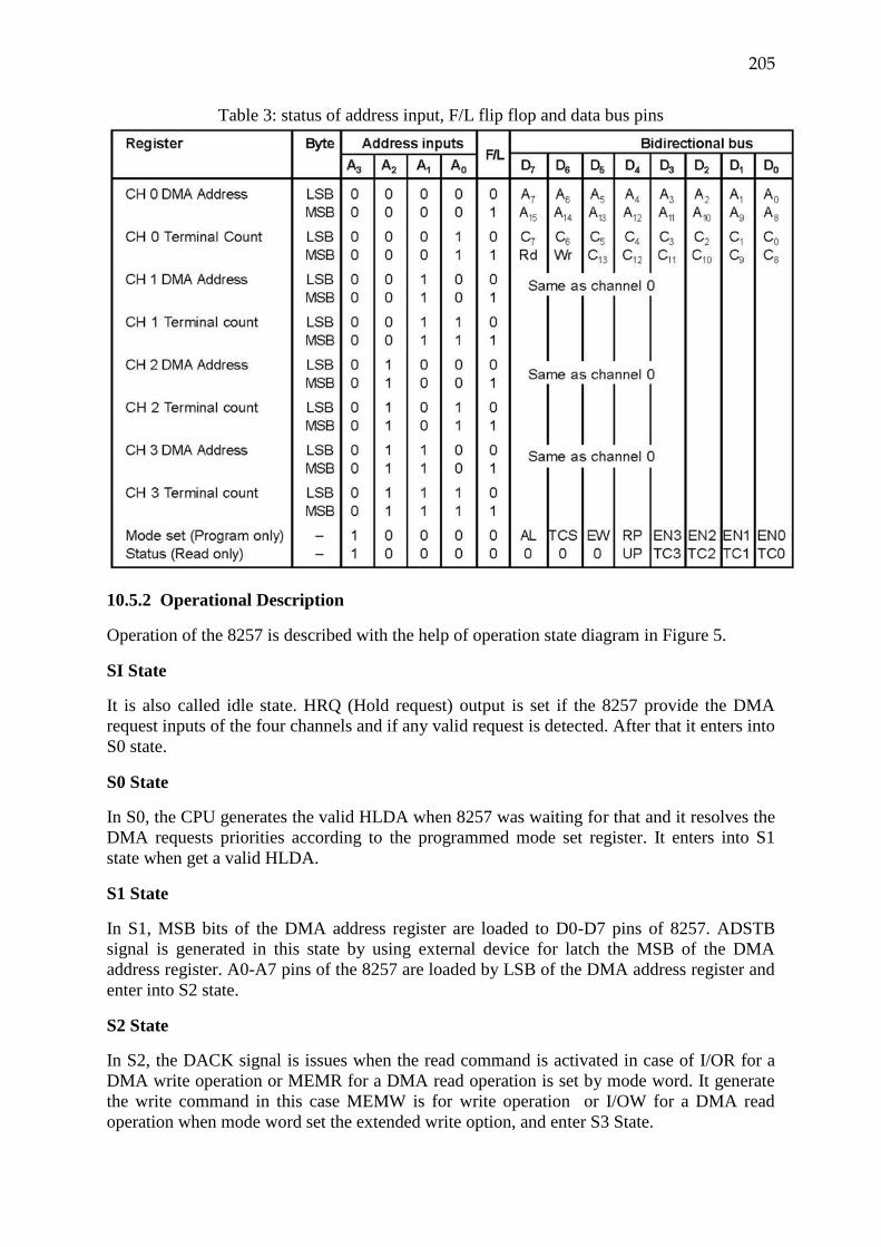
205
Table 3: status of address input, F/L flip flop and data bus pins
10.5.2 Operational Description
Operation of the 8257 is described with the help of operation state diagram in Figure 5.
SI State
It is also called idle state. HRQ (Hold request) output is set if the 8257 provide the DMA
request inputs of the four channels and if any valid request is detected. After that it enters into
S0 state.
S0 State
In S0, the CPU generates the valid HLDA when 8257 was waiting for that and it resolves the
DMA requests priorities according to the programmed mode set register. It enters into S1
state when get a valid HLDA.
S1 State
In S1, MSB bits of the DMA address register are loaded to D0-D7 pins of 8257. ADSTB
signal is generated in this state by using external device for latch the MSB of the DMA
address register. A0-A7 pins of the 8257 are loaded by LSB of the DMA address register and
enter into S2 state.
S2 State
In S2, the DACK signal is issues when the read command is activated in case of I/OR for a
DMA write operation or MEMR for a DMA read operation is set by mode word. It generate
the write command in this case MEMW is for write operation or I/OW for a DMA read
operation when mode word set the extended write option, and enter S3 State.
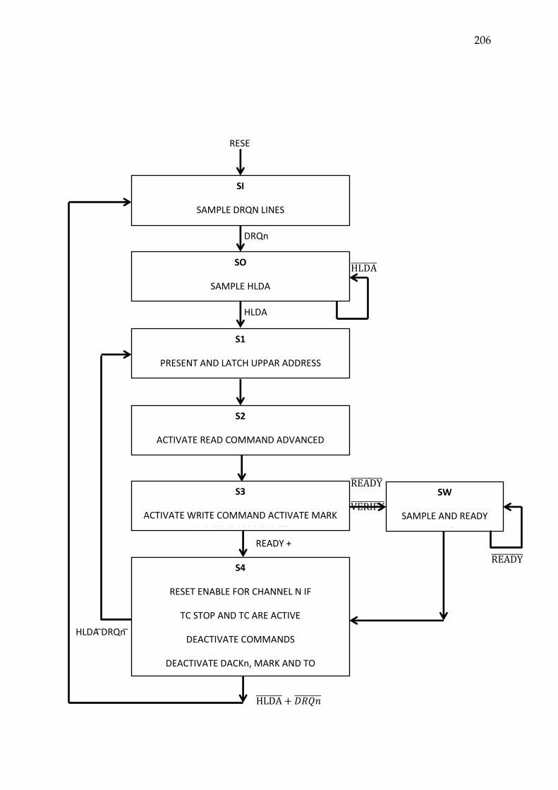
206
HLDA DRQn
SI
SAMPLE DRQN LINES
SET HRQ IF DRQN = 1
SO
SAMPLE HLDA
RESOLVE DRQN PRIORITIES
S1
PRESENT AND LATCH UPPAR ADDRESS
PRESENT LOWER ADDRESS
S2
ACTIVATE READ COMMAND ADVANCED
WRITE COMMAND AND DACKn
S3
ACTIVATE WRITE COMMAND ACTIVATE MARK
AND TC IF APPROPRITE
S4
RESET ENABLE FOR CHANNEL N IF
TC STOP AND TC ARE ACTIVE
DEACTIVATE COMMANDS
DEACTIVATE DACKn, MARK AND TO
SAMPLE DRQn AND HLDA
RESOLVE DREn PRIORITIES
RESET HRQn IF HLDA =0 0 OR DRQ=0
SW
SAMPLE AND READY
LINE
RESE
T
DRQn
HLDA
HLDA
READY
HLDA + 𝐷𝑅𝑄𝑛
READY +
VERIFY
READY
VERIFY
207
Figure 5: 8 DMA Operation State Diagram
S3 State
In S3, if write operation is not completed or if device is not ready to write data than ready
input of the 8257 will be set to low value and 8257 enters into wait state. It continues to work
in this state until a specific ready input is detected and after it enters into S4 state.
S4 State
The working status of channel is disabled if the TC stop option of the mode set register is set,
and if TC output is high. Some signals (DACK, TC and mark outputs) are deactivated.
Priority of DMA inputs are resolved by using sampling. It reset the Hold request (HRQ)
output, if no DMA requests are detected to the CPU and enter into SI state. If a valid DRQ
request for another channel (for Burst mode operation) is detected than after resolving their
priorities, the 8257 enters into SI state, and continues with DMA operation if HLDA is active.
8257 enters in SI state, if either a low HLDA is detected or DMA request is not detected. If
DRQ is detected and HLDA is in high in S4 state than it enters into SI from S4 state.
Single Byte Transfer
It is initiated by the I/O device raising the DRQ line of one channel of the 8257. If channel is
enabled than DMA controller enters into S2 state and process of execution in S1- S4 state
(see in Fig). In case of transfer operation, the selection of chip select for the I/O device is
from DACK output of the 8257. It is necessary that DRQ line must be kept high till a DACK
is received. In order to stop the 8257 from executing the other DMA cycle, the DRQ output
to the 8257 will be make low before S4.
Burst mode and Consecutive DMA transfer
In Burst mode, all the required number of bytes are transferred, until the I/O device make its
DRQ output low. If more than one channel simultaneously places its request for operation,
the request is are recognized and operated according to the priorities assigned. This is called
consecutive DMA transfer. In Burst mode, if channel is serviced in Burst mode than higher
priority DRQ serviced is first and 8257 returns into the lower priority DRQ in only case
where it will active.
Self-Assessment 1
1. In Intel 8257 DMA Controller each channel has
a) a pair of two 8-bit registers
b) a pair of two 16-bit registers
c) one 16-bit register and one 8-bit register
d) one 8-bit register
2. The common register(s) for all the four channels of 8257 are/is
208
a) Terminal Count (TC) register
b) DMA address register
c) Mode Set Register and Status Register
d) None of these
3. In 8257 register format, the selected channel is disabled after the terminal count
condition is reached when
a) Auto load is set
b) Auto load is reset
c) TC STOP bit is reset
d) TC STOP bit is set
4. The pin that requests the access of the system bus is
a) HLDA
b) HRQ
c) ADSTB
d) None of these
5. The pin that strobes the higher byte of the memory address, generated by the DMA
controller into the latches is
a) AEN
b) ADSTB
c) TC
d) None of these
Self-Assessment 2
1 Intel 8257 has how many modes of operation? What are they?
2 Write about the role of reset in DMA controller
3 Write about DMA ACK.
209
Self-Assessment 3
1 Intel 8257 has _________________ channels.
2 Hols is an _______________ signal
3 _______ shows that the MPU releasing the control buses
10.6 Answer to Check Your Progress/Suggested Answers to SAQ
Answers: Self-Assessment 1
1. (b) a pair of two 16-bit registers
2. (c) Mode Set Register and Status Register
3. (d) TC STOP bit is set
4. (b) HRQ
5. (b) ADSTB
Answers: Self-Assessment 2
1 . intel 8257 has 3 modes of operations.
DMA READ
DMA WRITE
DMA VERIFY
2. This is an asynchronous high input. It clears the mode set register to disable all DMA
channels and all states of controlled channels
3. These are active low outputs lines connected to channel. These lines are used to provide
acknowledgement in response to the peripheral request.
Answers: Self-Assessment 3
1 4
2 Active high input
3 HLDA
210
10.7 Bibliography/References/ Suggested Readings
1. Microprocessor Architecture, Programming and Applications with 8085, Ramesh. S.
Gaonkar, Fourth Edition, Penram International Publishing.
2. Microprocessors And Applications, D.A.Godse, A.P.Godse, First Edition, technical
Publications Pune.
10.8 Terminal and Model Questions
1. What is need for direct memory access (DMA) data transfer?
2. How many signals are used in DMA controller?
3. Discuss different types of mode of DMA controller.
4. Describe the functions of the pins of 8257.
5. Explain the functions of registers available in 8257.
6. What is use of flip flop in 8257?
7. Explain the function of A0-A3, IOR, IOW, MR, MW pins of 8257, when working in
slave mode.
8. Explain the function of A0-A3, IOR, IOW, MR, MW pins of 8257, when working in
master mode.
9. Explain single byte transfer and Burst mode transfer and consecutive DMA transfer.
10. Explain different types of option used in mode set register of 8257.
11. Explain the operation of 8257.
211
Chapter 11
Introduction to Programmable Interrupt Controller 8259
Architecture
Structure
11.0 Objectives
11.1 Introduction
11.2 Pin Description of 8259
11.3 Functional Description of 8259
11.4 8259 Programming
11.5 Initialization Command Words
11.6 Operation Command Words (OCWS)
11.7 Interrupt Modes
11.7.1 Fully Nested Mode
11.7.2 Special Mask Mode
11.7.3 Level and Edge Triggered Modes
11.7.4 The Special Fully Nest Mode
11.7.5 Buffered Mode
11.7.6 Cascaded Mode
11.8 Answer to Check Your Progress/Suggested Answers to SAQ
11.9 Bibliography/References/ Suggested Readings
11.10 Terminal and Model Questions
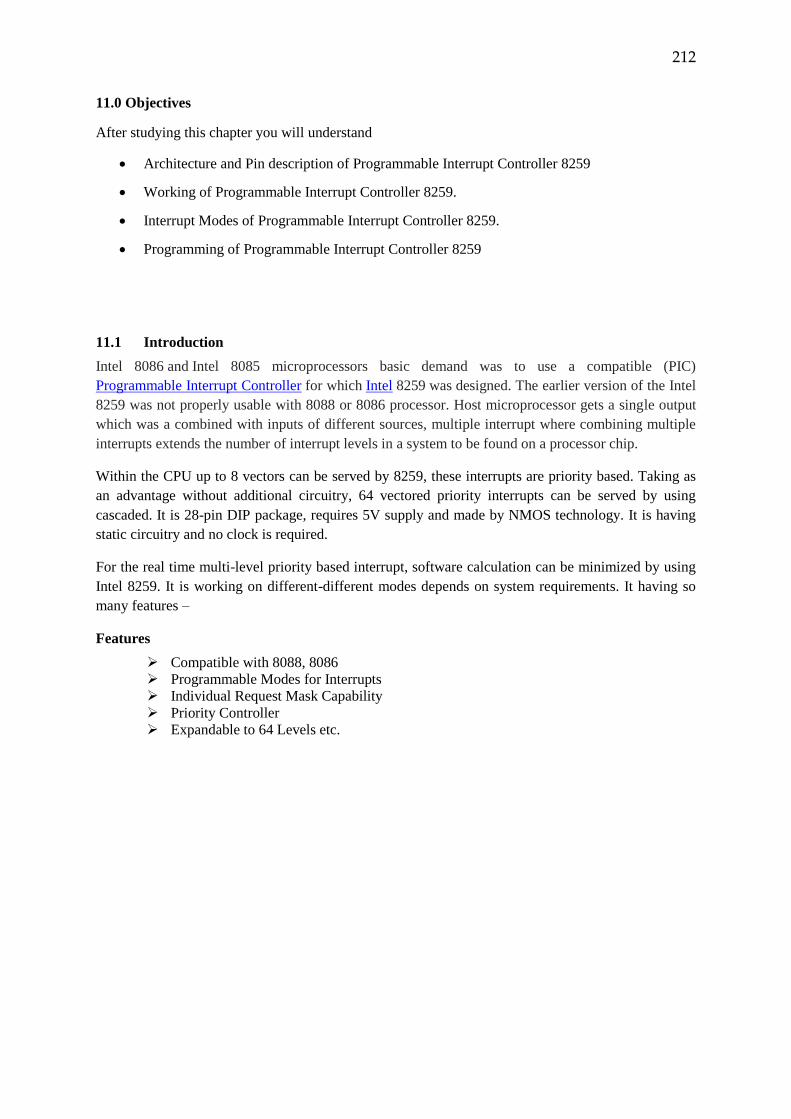
212
11.0 Objectives
After studying this chapter you will understand
Architecture and Pin description of Programmable Interrupt Controller 8259
Working of Programmable Interrupt Controller 8259.
Interrupt Modes of Programmable Interrupt Controller 8259.
Programming of Programmable Interrupt Controller 8259
11.1 Introduction
Intel 8086 and Intel 8085 microprocessors basic demand was to use a compatible (PIC)
Programmable Interrupt Controller for which Intel 8259 was designed. The earlier version of the Intel
8259 was not properly usable with 8088 or 8086 processor. Host microprocessor gets a single output
which was a combined with inputs of different sources, multiple interrupt where combining multiple
interrupts extends the number of interrupt levels in a system to be found on a processor chip.
Within the CPU up to 8 vectors can be served by 8259, these interrupts are priority based. Taking as
an advantage without additional circuitry, 64 vectored priority interrupts can be served by using
cascaded. It is 28-pin DIP package, requires 5V supply and made by NMOS technology. It is having
static circuitry and no clock is required.
For the real time multi-level priority based interrupt, software calculation can be minimized by using
Intel 8259. It is working on different-different modes depends on system requirements. It having so
many features –
Features
Compatible with 8088, 8086
Programmable Modes for Interrupts
Individual Request Mask Capability
Priority Controller
Expandable to 64 Levels etc.
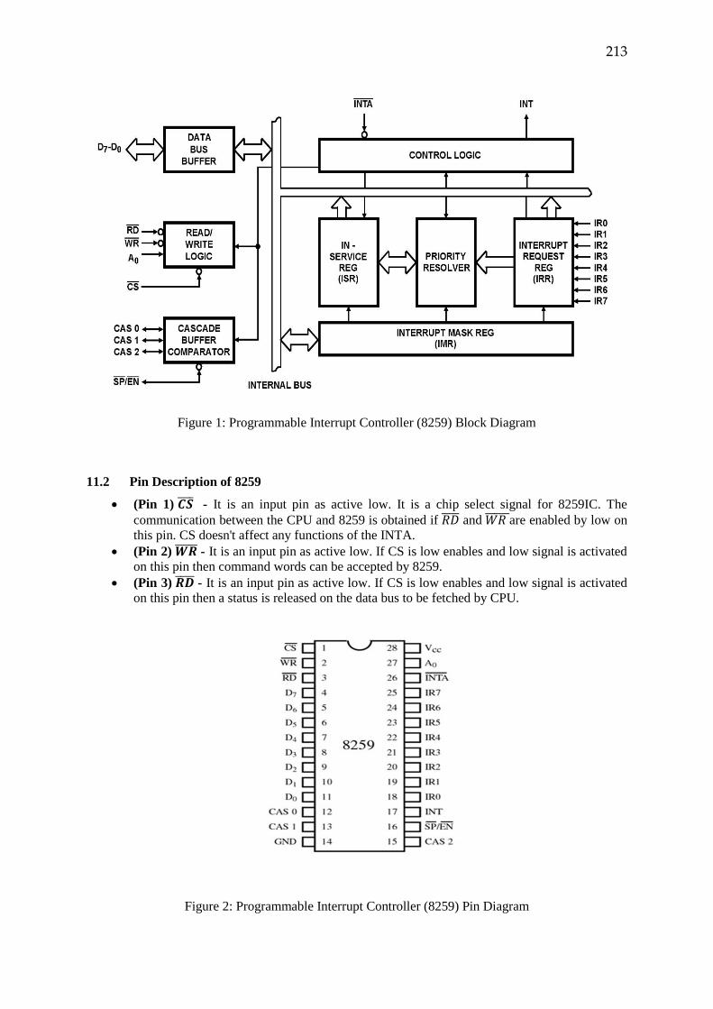
213
Figure 1: Programmable Interrupt Controller (8259) Block Diagram
11.2 Pin Description of 8259
(Pin 1) 𝑪𝑺 - It is an input pin as active low. It is a chip select signal for 8259IC. The
communication between the CPU and 8259 is obtained if 𝑅𝐷 and 𝑊𝑅 are enabled by low on
this pin. CS doesn't affect any functions of the INTA.
(Pin 2) 𝑾𝑹 - It is an input pin as active low. If CS is low enables and low signal is activated
on this pin then command words can be accepted by 8259.
(Pin 3) 𝑹𝑫 - It is an input pin as active low. If CS is low enables and low signal is activated
on this pin then a status is released on the data bus to be fetched by CPU.
Figure 2: Programmable Interrupt Controller (8259) Pin Diagram
214
(Pin to 11 ) D7-D0 - Vectored interrupts, information of status and control can be transferred
by using these bidirectional I/O data buses. (Pin 12,13,15) CAS0-CAS2 - CPU can be interfaced with multiple 8259 with the use of
these cascaded I/O line. These pins act as inputs for slave 8259 and outputs for a master
8259. (Pin 16) 𝑬𝑵 /𝑺𝑷 (Enable Buffer/Slave Program) - The need of using 8259 as a master or
slave can be decide by this pin. It is a pin for data function. Master and slave are decided by
putting 5V and 0V on this pin respectively. (EN) buffer transceivers or buffer for the system
data bus can be controlled /enabled if this pin is used as output pin when 8259 is used in
buffered mode. In case of non buffered mode this pin is operate as an input for slave or
master.
(Pin 17) INT (Interrupt) - It's an output pin as active high. If a valid interrupt request is
asserted than this pin goes high. CPU can be interrupted by enabling this pin.
(Pin 18 to 25) IR0-IR7 (Interrupt Requests) – These pins are used for interrupt requests
for master devices (8085/86). In the Edge triggered mode signal on these pins is low to high
and for Level triggered mode high level on these pins generate an interrupt requests.
(Pin 26) 𝑰𝑵𝑻𝑨 (Interrupt Acknowledge) – CPU issues a sequence pulses of interrupt
acknowledgement gets the interrupt vectored data of 8259 on the data bus which is done by
enabling this specified input pin.
(Pin 27) A0 (Address Line) –Various command words can be provided by using this input
pin of 8259 when CPU needs to read and write. Address line of the CPU is basically
connected to this pin.
(Pin28) VCC– 5v supply.
(Pin14) GND– GROUND.
Self-Assignment - 1
1) 8259 can handle ___ priority interrupts
a) 8 b) 16 c) 128 d) 64
2) 8259 have ___ pins
a) 32 b) 40 c) 28 d) 64
3) When cascaded mode is used?
11.3 Functional Description of 8259
In-Service Register (ISR) and Interrupt Request Register (IRR) – These two registers handle the
IR input line interrupts when (the In-Service and the Interrupt Request Register) are connected in
cascade. IRR is used to keep hold of the info about inputs requesting service of the interrupts and
serviced interrupt levels are stored by ISR.
Priority Resolver - When IRR sets multiple requesting service of interrupts, it helps in resolving the
priorities. As the INTA input is processed than particular input bit is selected in the ISR having the
highest priority.
215
IMR (Interrupt Mask Register) - The IMR stores the bits which are mask specific interrupts lines
with interrupt request having lower quality will not be affected by masking the input having higher
priority.
INT (Interrupt) - CPU interrupt line directly gets the output by this pin. The input levels of 8086,
8085A and 8080A are fully compatible with the designed voltage level on INT line.
𝑰𝑵𝑻𝑨 (Interrupt Acknowledge) – With the help of this pin, 8259 to data bus gets the vector
information. The system mode of the 8259 decide the format of this data.
Data Bus Buffer - It is 8-bit bidirectional buffer with three states. System Data Bus can be interfaced
by using this type of buffer. Status information and Control words are bypasses the Data Bus Buffer.
Read/Write Control Logic –Output commands are accepted by this block which comes from the
CPU. For the device operation, various control formats can be stored by this block as it consists of
Operation Command Word (OCW) registers and Initialization Command Word (ICW) registers, both
can be programmed by the CPU. Read commands are also accepted by this block which comes from
the CPU for permitting the reading of status words by CPU.
Cascade Buffer/Comparator - When we are using multiple 8259 ICs cascade buffer mode is used.
The 8259 can be cascaded with another 8257s in order for increasing the capacity of interrupt
handling, 8257s are cascaded with another 8259. In this case, the first 8259 is called master and last
one is slaves. When multiple 8259 are connected in the system, this block compares and stores the
IDs of every connected block. When the 8259 is used as a slave the (CAS0-2) associated three I/O
pins acts as inputs and outputs when the 8259 is used as a master.
11.4 8259 Programming
CPU generates two types of commands accepted by 8259:
1. (ICWs) Initialization Command Words: ICWs set up the 8259 to operate according to system
specifications. Every 8259 connected in the system must be brought to initial stage by using a
array of 4 to 2 bytes which are timed by the write pulses before the beginning of every normal
operation. Each 8259 in the system must be initialized through ICWs. These are described in
flow chart shown in fig.
2. (OCWs) Operation Command Words: 8259 operates in various interrupt modes which are
defined by certain command words. These modes are-
End of Interrupt
Fully nested mode
Automatic End of Interrupt (AEOI)
Specific Rotation (Specific Priority)
Automatic Rotation (Equal Priority Devices
Polled mode
Special Mask Mode
Special Fully Nest Mode
Edge and Level Triggered Modes
Buffered Mode
Cascaded Mode.
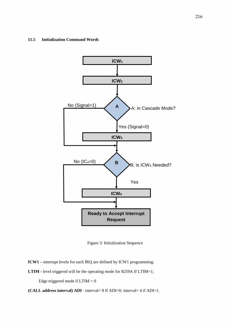
216
11.5 Initialization Command Words
Figure 3: Initialization Sequence
ICW1 – interrupt levels for each IRQ are defined by ICW1 programming.
LTIM - level triggered will be the operating mode for 8259A If LTIM=1;
Edge triggered mode if LTIM = 0
(CALL address interval) ADI - interval= 8 If ADI=0; interval= 4 if ADI=1.
Yes
No (IC4=0) B: is ICW4 Needed?
Yes (Signal=0)
ICW1
A
B
ICW2
ICW3
ICW4
Ready to Accept Interrupt
Request
No (Signal=1) A: in Cascade Mode?
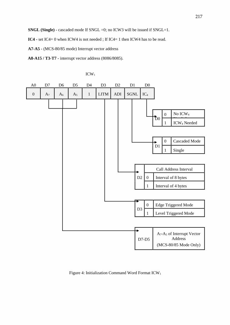
217
SNGL (Single) - cascaded mode If SNGL =0; no ICW3 will be issued if SNGL=1.
IC4 - set IC4= 0 when ICW4 is not needed ; If IC4= 1 then ICW4 has to be read.
A7-A5 - (MCS-80/85 mode) Interrupt vector address
A8-A15 / T3-T7 - interrupt vector address (8086/8085).
ICW1
A0 D7 D6 D5 D4 D3 D2 D1 D0
0 A7 A6 A5 1 LITM ADI SGNL IC4
D0 0 No ICW4
Needed 1 ICW4 Needed
D1
0 Cascaded Mode
1 Single
D2
Call Address Interval
0 Interval of 8 bytes
1 Interval of 4 bytes
D3 0 Edge Triggered Mode
1 Level Triggered Mode
D7-D5
A7-A5 of Interrupt Vector
Address
(MCS-80/85 Mode Only)
Figure 4: Initialization Command Word Format ICW1
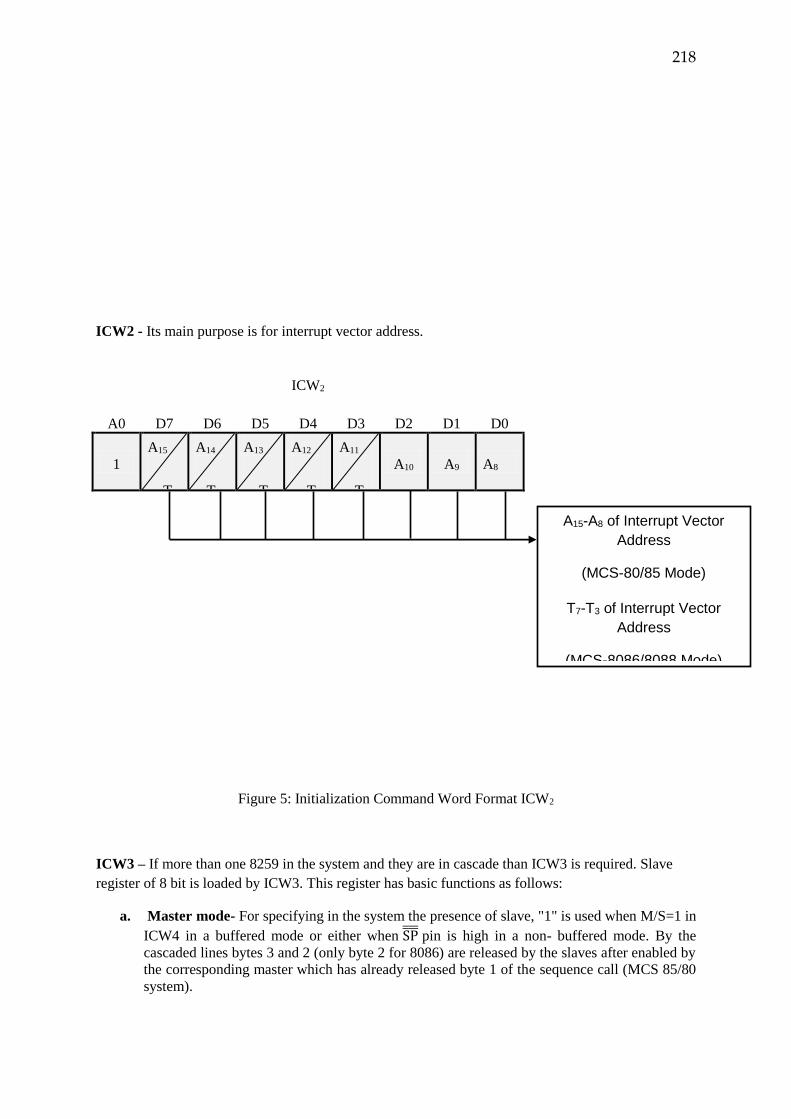
218
ICW2 - Its main purpose is for interrupt vector address.
ICW2
A0 D7 D6 D5 D4 D3 D2 D1 D0
1
A15
T7
A14
T6
A13
T5
A12
T4
A11
T3
A10 A9 A8
Figure 5: Initialization Command Word Format ICW2
ICW3 – If more than one 8259 in the system and they are in cascade than ICW3 is required. Slave
register of 8 bit is loaded by ICW3. This register has basic functions as follows:
a. Master mode- For specifying in the system the presence of slave, "1" is used when M/S=1 in
ICW4 in a buffered mode or either when SP pin is high in a non- buffered mode. By the
cascaded lines bytes 3 and 2 (only byte 2 for 8086) are released by the slaves after enabled by
the corresponding master which has already released byte 1 of the sequence call (MCS 85/80
system).
A15-A8 of Interrupt Vector
Address
(MCS-80/85 Mode)
T7-T3 of Interrupt Vector
Address
(MCS-8086/8088 Mode)
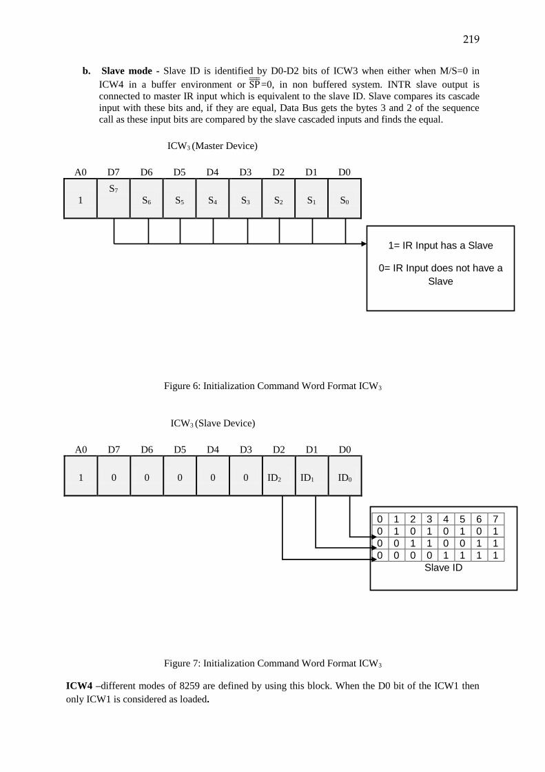
219
b. Slave mode - Slave ID is identified by D0-D2 bits of ICW3 when either when M/S=0 in
ICW4 in a buffer environment or SP =0, in non buffered system. INTR slave output is
connected to master IR input which is equivalent to the slave ID. Slave compares its cascade
input with these bits and, if they are equal, Data Bus gets the bytes 3 and 2 of the sequence
call as these input bits are compared by the slave cascaded inputs and finds the equal.
ICW3 (Master Device)
A0 D7 D6 D5 D4 D3 D2 D1 D0
1
S7
S6 S5 S4 S3 S2 S1 S0
Figure 6: Initialization Command Word Format ICW3
ICW3 (Slave Device)
A0 D7 D6 D5 D4 D3 D2 D1 D0
1 0 0 0 0 0 ID2 ID1 ID0
Figure 7: Initialization Command Word Format ICW3
ICW4 –different modes of 8259 are defined by using this block. When the D0 bit of the ICW1 then
only ICW1 is considered as loaded.
1= IR Input has a Slave
0= IR Input does not have a
Slave
0 1 2 3 4 5 6 7
0 1 0 1 0 1 0 1
0 0 1 1 0 0 1 1
0 0 0 0 1 1 1 1
Slave ID
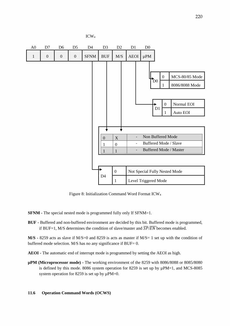
220
ICW4
A0 D7 D6 D5 D4 D3 D2 D1 D0
1 0 0 0 SFNM BUF M/S AEOI µPM
D0 0 MCS-80/85 Mode
1 8086/8088 Mode
D1 0 Normal EOI
1 Auto EOI
Figure 8: Initialization Command Word Format ICW4
SFNM - The special nested mode is programmed fully only If SFNM=1.
BUF - Buffered and non-buffered environment are decided by this bit. Buffered mode is programmed,
if BUF=1, M/S determines the condition of slave/master and 𝑆𝑃 /𝐸𝑁 becomes enabled.
M/S - 8259 acts as slave if M/S=0 and 8259 is acts as master if M/S= 1 set up with the condition of
buffered mode selection. M/S has no any significance if BUF= 0.
AEOI - The automatic end of interrupt mode is programmed by setting the AEOI as high.
µPM (Microprocessor mode) - The working environment of the 8259 with 8086/8088 or 8085/8080
is defined by this mode. 8086 system operation for 8259 is set up by µPM=1, and MCS-8085
system operation for 8259 is set up by µPM=0.
11.6 Operation Command Words (OCWS)
0 X - Non Buffered Mode
1 0 - Buffered Mode / Slave
1 1 - Buffered Mode / Master
D4 0 Not Special Fully Nested Mode
1 Level Triggered Mode
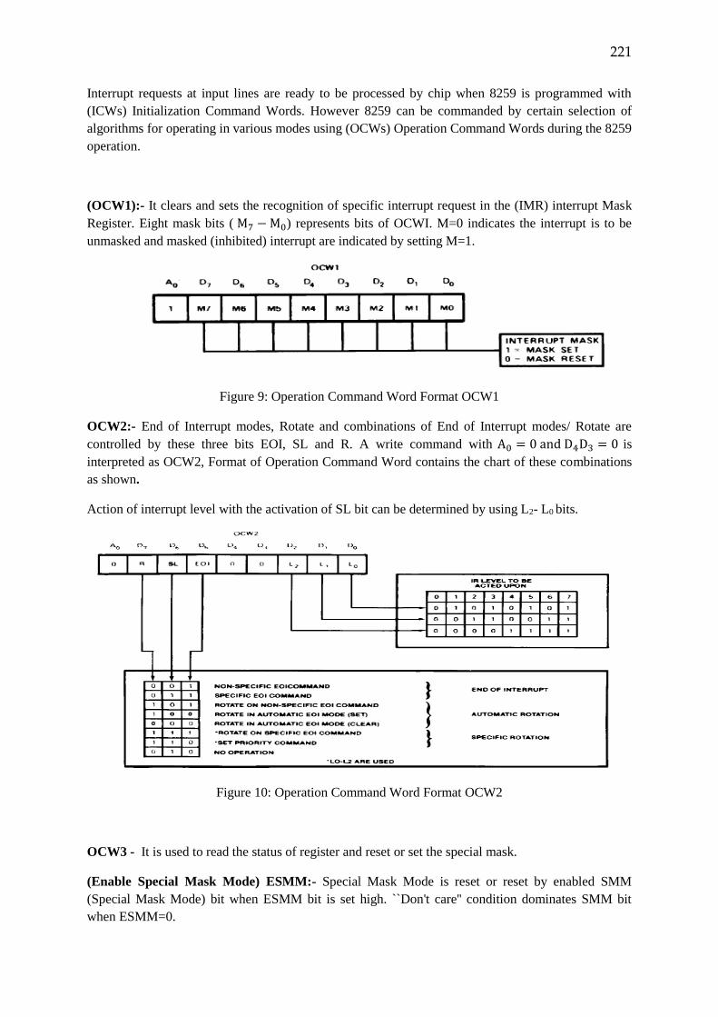
221
Interrupt requests at input lines are ready to be processed by chip when 8259 is programmed with
(ICWs) Initialization Command Words. However 8259 can be commanded by certain selection of
algorithms for operating in various modes using (OCWs) Operation Command Words during the 8259
operation.
(OCW1):- It clears and sets the recognition of specific interrupt request in the (IMR) interrupt Mask
Register. Eight mask bits ( M7 − M0) represents bits of OCWI. M=0 indicates the interrupt is to be
unmasked and masked (inhibited) interrupt are indicated by setting M=1.
Figure 9: Operation Command Word Format OCW1
OCW2:- End of Interrupt modes, Rotate and combinations of End of Interrupt modes/ Rotate are
controlled by these three bits EOI, SL and R. A write command with A0 = 0 and D4D3 = 0 is
interpreted as OCW2, Format of Operation Command Word contains the chart of these combinations
as shown.
Action of interrupt level with the activation of SL bit can be determined by using L2- L0 bits.
Figure 10: Operation Command Word Format OCW2
OCW3 - It is used to read the status of register and reset or set the special mask.
(Enable Special Mask Mode) ESMM:- Special Mask Mode is reset or reset by enabled SMM
(Special Mask Mode) bit when ESMM bit is set high. ``Don't care'' condition dominates SMM bit
when ESMM=0.
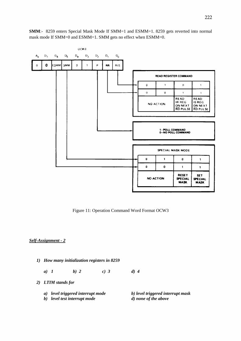
222
SMM:- 8259 enters Special Mask Mode If SMM=1 and ESMM=1. 8259 gets reverted into normal
mask mode If SMM=0 and ESMM=1. SMM gets no effect when ESMM=0.
Figure 11: Operation Command Word Format OCW3
Self-Assignment - 2
1) How many initialization registers in 8259
a) 1 b) 2 c) 3 d) 4
2) LTIM stands for
a) level triggered interrupt mode b) level triggered interrupt mask
b) level test interrupt mode d) none of the above
223
3) Function of µpm?
11.7 Interrupt Modes
11.7.1 Fully Nested Mode (FNM)
After the initialization 8259 enters this mode. Fully nested mode is the operating mode for 8259 until
(OCWs) operations command words changes the operating mode. Priorities from 0 through 7 (7
lowest and 0 highest) are assigned to interrupt requests. Vector interrupt address set and put up on the
bus as highest priority is determined by 8259 after the acknowledgement of interrupt. Setting of (ISO-
7) Interrupt Service register takes place. Before getting from initial state of service routine, this bit
still remains set till an EOI (End of Interrupt) command is executed. Until the trailing edge of last
INTA gets passed through , it keeps the (Automatic End of Interrupt)AEOI bit high. Higher priority
interrupts generates an interrupts whereas all the lower priority interrupts gets inhibited while IS bit is
high (Software re-enable the enabled internal Interrupt flip-flop of microprocessor which shows the
acknowledgement).
IR7 has the lowest priority and IR0 the lowest right after the initialization sequence. In rotating
priority mode, priorities can be explained as well as changed.
EOI (End of Interrupt) – In ICW1 command register when AEOI bit is set, following the last
sequence of trailing edge of 𝐼𝑁𝑇𝐴 pulse or by a EOI command (IS) In Service bit can be reset either
automatically .In Cascade mode command for EOI must be issued two times, one for the
corresponding slave and second for the master.
EOI command has particularly two forms: Non-Specific and Specific. Keeping the bit OCW2 (EOI =
1, SL = 0, R =0) issues a non-specific EOI command. For preserving the fully nested structure EOI
mode is used, determines reset IS bit on EOI. 8259 reset the highest set IS bit by using Non Specific
EOI command.
Specific End of Interrupt must be issued when fully nested structure is in danger i.e. working mode of
8259 overcomes the utility of fully nested structure and the last served interrupt may not be able to be
determined by 8259. OCW2 (R=0,SL=1, EOI =1, and binary level of the IS bit to be reset L0- L2) can
issue a specific EOI.
One thing should be remember that an IMR masked bit cannot be cleaned by unspecified functions,
when 8259 is working in Special Mask Mode.
Automatic End of Interrupt (AEOI) – Within ICW4 AEOI is set, 8259 will operate continuously in
this mode until ICW4 reprogrammed. Trailing edge of the last acknowledged interrupt, a non
specified EOI operation is performed automatically by 8259 in the AEOI mode. This mode can be
used for master. When there is no need of the multilevel structure of nested interrupts then it's useful
for single 8259.
Automatic Rotation (Equal Priority Devices) –This mode is used when number of interrupt devices
having same priorities. In this mode each device served at once and get the lowest priority after served
and wait for next round until all the higher priorities are being served . Following example describes
this mode sequence:
(highest priority requiring service IR4) Before Rotate
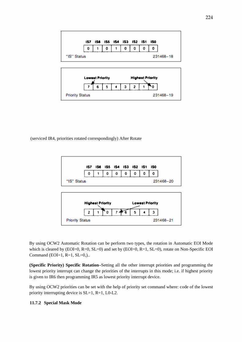
224
(serviced IR4, priorities rotated correspondingly) After Rotate
By using OCW2 Automatic Rotation can be perform two types, the rotation in Automatic EOI Mode
which is cleared by (EOI=0, R=0, SL=0) and set by (EOI=0, R=1, SL=0), rotate on Non-Specific EOI
Command (EOI=1, R=1, SL=0,)..
(Specific Priority) Specific Rotation–Setting all the other interrupt priorities and programming the
lowest priority interrupt can change the priorities of the interrupts in this mode; i.e. if highest priority
is given to IR6 then programming IR5 as lowest priority interrupt device.
By using OCW2 priorities can be set with the help of priority set command where: code of the lowest
priority interrupting device is SL=1, R=1, L0-L2.
11.7.2 Special Mask Mode
225
Interrupt service routine might be required, under software control for some applications which are
dynamically altering the priority structure of the system during its execution.
The main difficulty here is that if an Interrupt Request is acknowledged, while executing a service
routine and an End of Interrupt command did not reset its IS bit than the 8259 would have inhibited
all lower priority requests with no easy way for the routine to enable them.
The Special Mask Mode is to be set by masking the SSMM and SMM bits “1” in OCW3. In the
special Mask Mode, when a mask bit is set in OCW1, all further interrupts at that level are inhibited,
while interrupts from all other levels (lower as well as higher) that are not masked. Thus, any
interrupts may be selectively enabled by loading the mask register.
OWC3 sets special Mask Mode cleared where SMM=0, SSMM=1 and where: SMM=1, SSMM=1.
Poll Command -In this mode the INT output functions as it normally does. The microprocessor
should ignore this output. This can be accomplished either by not connecting the INT output or by
masking interrupts within the microprocessor, thereby disabling its interrupt input. Service to devices
is achieved by software using a Poll command. The Poll command is issued by setting P=1in OCW3.
Since the INTR line is not used in this mode, more 8259 may be connected in the master mode, use
the poll mode to expand the number of priority levels to more than 64.
11.7.3 Level and Edge Triggered Modes
Using ICW1 3 bits, programming of this mode is an easy task. If LTIM=0, than on an IR input low to
high transition does and generation of an interrupt request takes place. Without the generation of
another interrupt, IR input can remain set high.
Edge detection won't be needed on IR input, high level shows the presence of interrupt request if
LTIM=1. For preventing the occurrence of second interrupt, CPU interrupt is enabled of before
issuing the EOI command there is need of removal of interrupt request.
11.7.4 The Special Fully Nest Mode
This mode is used for big systems, each slave must conserve the priority where many systems are
connected in cascade (using ICW4). By the use of fully nested mode, Master 8259 will be
programmed. Fully nested mode have some exceptions with lots of similarity to normal nested mode:
a. When interruption takes place while serving a slave and priority logic of master doesn't lock
out the slave but master recognizes the other higher priority interrupts of slave 8259 and
interrupts command to the processor is to be generated. When no higher priority interrupt
requests can be serviced sent by a slave then only slave is masked out in normal nested mode
with the interrupt request is serviced by the device.
b. When a slave sends an interrupt request, then it is checked by the software during service
routine of interrupts. Slave is checked by a non specified EOI command and then checking
for by using its IS(In-service) register. Master can also receive non-specific (EOI) End of
Interrupt if IS seems empty. No End of Interrupt (EOI) should be sent if it is not empty.
11.7.5 Buffered Mode
Large no of buffers are used and also data bus are required for driving these buffers therefore the
problem of enabling these buffers only when the 8259 is used in a cascading mode.
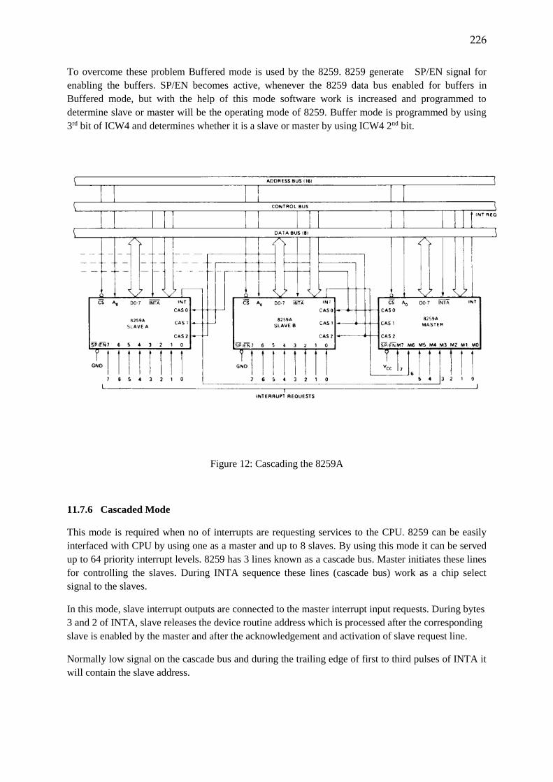
226
To overcome these problem Buffered mode is used by the 8259. 8259 generate SP/EN signal for
enabling the buffers. SP/EN becomes active, whenever the 8259 data bus enabled for buffers in
Buffered mode, but with the help of this mode software work is increased and programmed to
determine slave or master will be the operating mode of 8259. Buffer mode is programmed by using
3rd bit of ICW4 and determines whether it is a slave or master by using ICW4 2nd bit.
Figure 12: Cascading the 8259A
11.7.6 Cascaded Mode
This mode is required when no of interrupts are requesting services to the CPU. 8259 can be easily
interfaced with CPU by using one as a master and up to 8 slaves. By using this mode it can be served
up to 64 priority interrupt levels. 8259 has 3 lines known as a cascade bus. Master initiates these lines
for controlling the slaves. During INTA sequence these lines (cascade bus) work as a chip select
signal to the slaves.
In this mode, slave interrupt outputs are connected to the master interrupt input requests. During bytes
3 and 2 of INTA, slave releases the device routine address which is processed after the corresponding
slave is enabled by the master and after the acknowledgement and activation of slave request line.
Normally low signal on the cascade bus and during the trailing edge of first to third pulses of INTA it
will contain the slave address.
227
Each 8259 in the system can be programmed for different modes and must follow different-different
initialization sequences for interrupts. Two EOI commands for the slave and corresponding master
must be issued. For activation of chip select signal of 8259 an address decoder is required. 8259
connection in cascade mode is shown in Figure 12.
Self-Assignment - 3
1) EOI stands for
a) Edge of interrupt b) End of interrupt
c) End of initialization d) Edge of finalization
2) By using which initialization register is used for Level and Edge triggered mode
a) ICW1 b) ICW2 c) ICW3 d) ICW4
3) What is Buffered Mode?
17.8 Answer to Check Your Progress/Suggested Answers to SAQ
Self-Assignment 1 Answer
1. ANS - d
2. ANS - c
3. ANS - Cascaded mode is used for more than one 8259.
Self-Assignment 2 Answer
1. ANS - d
2. ANS- a
3. ANS - It is used for microprocessor mode(8085/86).
Self-Assignment 3 Answer
1. ANS - b
2. ANS - a
3. ANS - Buffered mode is used in cascade mode for enabling the buffers.
228
11.9 Bibliography/References/Suggested Readings:
1.Microprocessor Architecture, Programming and Applications with 8085, Ramesh. S.
Gaonkar, Fourth Edition, Penram International Publishing.
2.Microprocessors And Applications, D.A.Godse, A.P.Godse, First Edition, technical
Publications Pune.
11.10 Terminal and Model Questions
1. Draw the pin diagram of 8259 interrupt controller and explain each pin.
2. Draw the block diagram of Intel 8259 interrupt controller and explain it.
3. Explain different type of interrupt modes in 8259.
229
Chapter 12
Introduction to Clock Generator 8284 Architecture
Structure
12.0 Objectives
12.1 Introduction to 8284 Clock Generator
12.2 Pin Configuration of 8284 Clock Generator IC
12.3 Block Diagram of Intel 8284 Clock Generator
12.3.1 Oscillator
12.3.2 Clock Generator
12.3.3 Output Clock
12.3.4 Reset Logic
12.3.5 Ready Synchronization
12.4 8284 Clock Generator Operation
12.4.1 Operation of the clock section:
12.4.2 Operation of the Reset section
12.5 Answer to Check Your Progress/Suggested Answers to SAQ
12.6 Bibliography/References/ Suggested Readings
12.7 Terminal and Model Questions
12.0 Objectives
After studying this chapter you will understand
Architecture and Pin description of Intel 8284 Clock Generator.
Working of Intel 8284 Clock Generator.
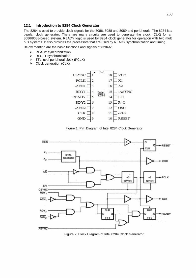
230
12.1 Introduction to 8284 Clock Generator
The 8284 is used to provide clock signals for the 8086, 8088 and 8089 and peripherals. The 8284 is a bipolar clock generator. There are many circuits are used to generate the clock (CLK) for an 8086/8088-based system. READY logic is used by 8284 clock generator for operation with two multi bus systems. It also provides the processors that are used by READY synchronization and timing.
Below mention are the basic functions and signals of 8284A:
READY synchronization RESET synchronization TTL level peripheral clock (PCLK) Clock generation (CLK)
Figure 1: Pin Diagram of Intel 8284 Clock Generator
Figure 2: Block Diagram of Intel 8284 Clock Generator
231
12.2 Pin Configuration of 8284 Clock Generator IC
8284 clock generator pin diagram is shown in Figure 1.
𝑹𝑬𝑺 (RESET IN): It is an active low input signal. The 8284 used this pin to generate RESET IN signal. Power supply of the microprocessor is connected to this pin. A low signal is generated on the RES in the case of “ON” state of microprocessor.
X1 and X2 (Crystal inputs): These are two input pins, which are used to generate the required frequency when crystal is attached to crystal oscillator. The frequency of the crystal is three times more than required frequency.
CSYNC (Clock synchronization): This is an active low input signal. It is used to provide clock for synchronization, when more than one 8284 are connected together. The internal counters are reset, when CSYNC is high. When this signal is low than internal counters are allowed to resume counting.
F/�� (Frequency/Crystal select): The crystal oscillator or external source is used to generate clock in 8284. This pin is used to select an internal or external clock. Clock is generated by the 8284, if this pin is in low state and when this pin is high than external source will generate the clocks and applied through the EFI pin.
EFI (External Frequency In): If F/C logic is in high state i.e. 1 than CLK is generated from the input frequency appearing on that pin. Since internal clock frequency is used in microprocessor so this pin is not generally used.
RDY1 and 𝑨𝑬𝑵𝟏 : These are two input signals of 8284. First one (RDY1) is active high and second one (AEN1) is active low signal. READY signal of microprocessor are generated by using these two pins together.
RDY2 and𝑨𝑬𝑵𝟐 : The functions of these pins are same as RDY1 and AEN1. The use of this pin is to cause wait state. These additional pins are used in multiprocessing system.
RESET: It is used to reset the 8086 processors; It is an active high output signal.
PCLK (Peripheral Clock): The output frequency of peripheral clock signal (PCLK) is half that of CLK and has a 50% duty cycle.
OSC (Oscilloscope Clock): This pin is the output of the internal oscillator circuitry, whose frequency is equal to that of the crystal. This pin is used to generate an EFI input to other 8284 clock generators in some multiprocessor systems.
GND: ground
𝐕𝐜𝐜: +5V supply
Assignment 1 1. What is 8284 clock generator?
___________________________________________________________________________________________________________________________________________________________________________________________________________________________
2. How many pins are used in 8284 clock generator? Discuss the functions of CSYNC and F/C pins. ___________________________________________________________________________________________________________________________________________________________________________________________________________________________
3. RESET is a. Active low c. Both active low and Active high b. Active high d. None
4. Power supply of the microprocessor is connected to......... pin.
a. EFI c. RES b. OSC d. F/C
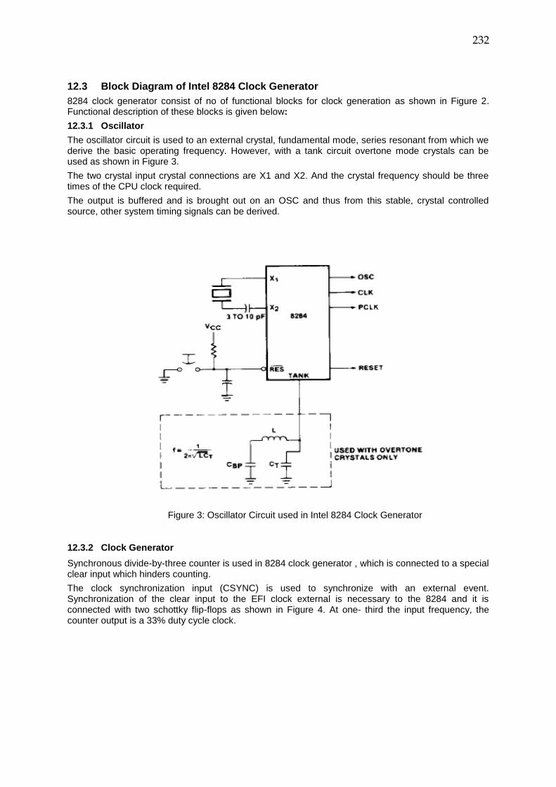
232
12.3 Block Diagram of Intel 8284 Clock Generator
8284 clock generator consist of no of functional blocks for clock generation as shown in Figure 2. Functional description of these blocks is given below:
12.3.1 Oscillator
The oscillator circuit is used to an external crystal, fundamental mode, series resonant from which we derive the basic operating frequency. However, with a tank circuit overtone mode crystals can be used as shown in Figure 3.
The two crystal input crystal connections are X1 and X2. And the crystal frequency should be three times of the CPU clock required.
The output is buffered and is brought out on an OSC and thus from this stable, crystal controlled source, other system timing signals can be derived.
Figure 3: Oscillator Circuit used in Intel 8284 Clock Generator
12.3.2 Clock Generator
Synchronous divide-by-three counter is used in 8284 clock generator , which is connected to a special clear input which hinders counting.
The clock synchronization input (CSYNC) is used to synchronize with an external event. Synchronization of the clear input to the EFI clock external is necessary to the 8284 and it is connected with two schottky flip-flops as shown in Figure 4. At one- third the input frequency, the counter output is a 33% duty cycle clock.
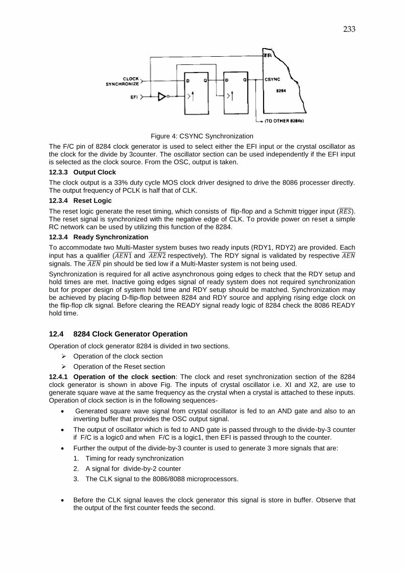
233
Figure 4: CSYNC Synchronization
The F/C pin of 8284 clock generator is used to select either the EFI input or the crystal oscillator as the clock for the divide by 3counter. The oscillator section can be used independently if the EFI input is selected as the clock source. From the OSC, output is taken.
12.3.3 Output Clock
The clock output is a 33% duty cycle MOS clock driver designed to drive the 8086 processer directly. The output frequency of PCLK is half that of CLK.
12.3.4 Reset Logic
The reset logic generate the reset timing, which consists of flip-flop and a Schmitt trigger input (𝑅𝐸𝑆 ). The reset signal is synchronized with the negative edge of CLK. To provide power on reset a simple RC network can be used by utilizing this function of the 8284.
12.3.4 Ready Synchronization
To accommodate two Multi-Master system buses two ready inputs (RDY1, RDY2) are provided. Each
input has a qualifier (𝐴𝐸𝑁1 and 𝐴𝐸𝑁2 respectively). The RDY signal is validated by respective 𝐴𝐸𝑁
signals. The 𝐴𝐸𝑁 pin should be tied low if a Multi-Master system is not being used.
Synchronization is required for all active asynchronous going edges to check that the RDY setup and hold times are met. Inactive going edges signal of ready system does not required synchronization but for proper design of system hold time and RDY setup should be matched. Synchronization may be achieved by placing D-flip-flop between 8284 and RDY source and applying rising edge clock on the flip-flop clk signal. Before clearing the READY signal ready logic of 8284 check the 8086 READY hold time.
12.4 8284 Clock Generator Operation
Operation of clock generator 8284 is divided in two sections.
Operation of the clock section
Operation of the Reset section
12.4.1 Operation of the clock section: The clock and reset synchronization section of the 8284 clock generator is shown in above Fig. The inputs of crystal oscillator i.e. XI and X2, are use to generate square wave at the same frequency as the crystal when a crystal is attached to these inputs. Operation of clock section is in the following sequences-
Generated square wave signal from crystal oscillator is fed to an AND gate and also to an inverting buffer that provides the OSC output signal.
The output of oscillator which is fed to AND gate is passed through to the divide-by-3 counter if F/C is a logic0 and when F/C is a logic1, then EFI is passed through to the counter.
Further the output of the divide-by-3 counter is used to generate 3 more signals that are:
1. Timing for ready synchronization
2. A signal for divide-by-2 counter
3. The CLK signal to the 8086/8088 microprocessors.
Before the CLK signal leaves the clock generator this signal is store in buffer. Observe that the output of the first counter feeds the second.
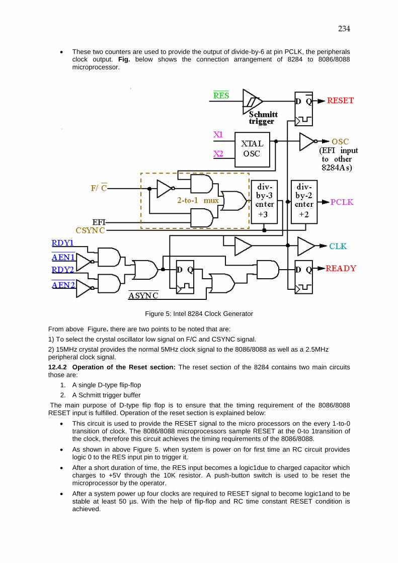
234
These two counters are used to provide the output of divide-by-6 at pin PCLK, the peripherals clock output. Fig. below shows the connection arrangement of 8284 to 8086/8088 microprocessor.
Figure 5: Intel 8284 Clock Generator
From above Figure. there are two points to be noted that are:
1) To select the crystal oscillator low signal on F/C and CSYNC signal.
2) 15MHz crystal provides the normal 5MHz clock signal to the 8086/8088 as well as a 2.5MHz peripheral clock signal.
12.4.2 Operation of the Reset section: The reset section of the 8284 contains two main circuits those are:
1. A single D-type flip-flop
2. A Schmitt trigger buffer
The main purpose of D-type flip flop is to ensure that the timing requirement of the 8086/8088 RESET input is fulfilled. Operation of the reset section is explained below:
This circuit is used to provide the RESET signal to the micro processors on the every 1-to-0 transition of clock. The 8086/8088 microprocessors sample RESET at the 0-to 1transition of the clock, therefore this circuit achieves the timing requirements of the 8086/8088.
As shown in above Figure 5. when system is power on for first time an RC circuit provides logic 0 to the RES input pin to trigger it.
After a short duration of time, the RES input becomes a logic1due to charged capacitor which charges to +5V through the 10K resistor. A push-button switch is used to be reset the microprocessor by the operator.
After a system power up four clocks are required to RESET signal to become logic1and to be stable at least 50 µs. With the help of flip-flop and RC time constant RESET condition is achieved.
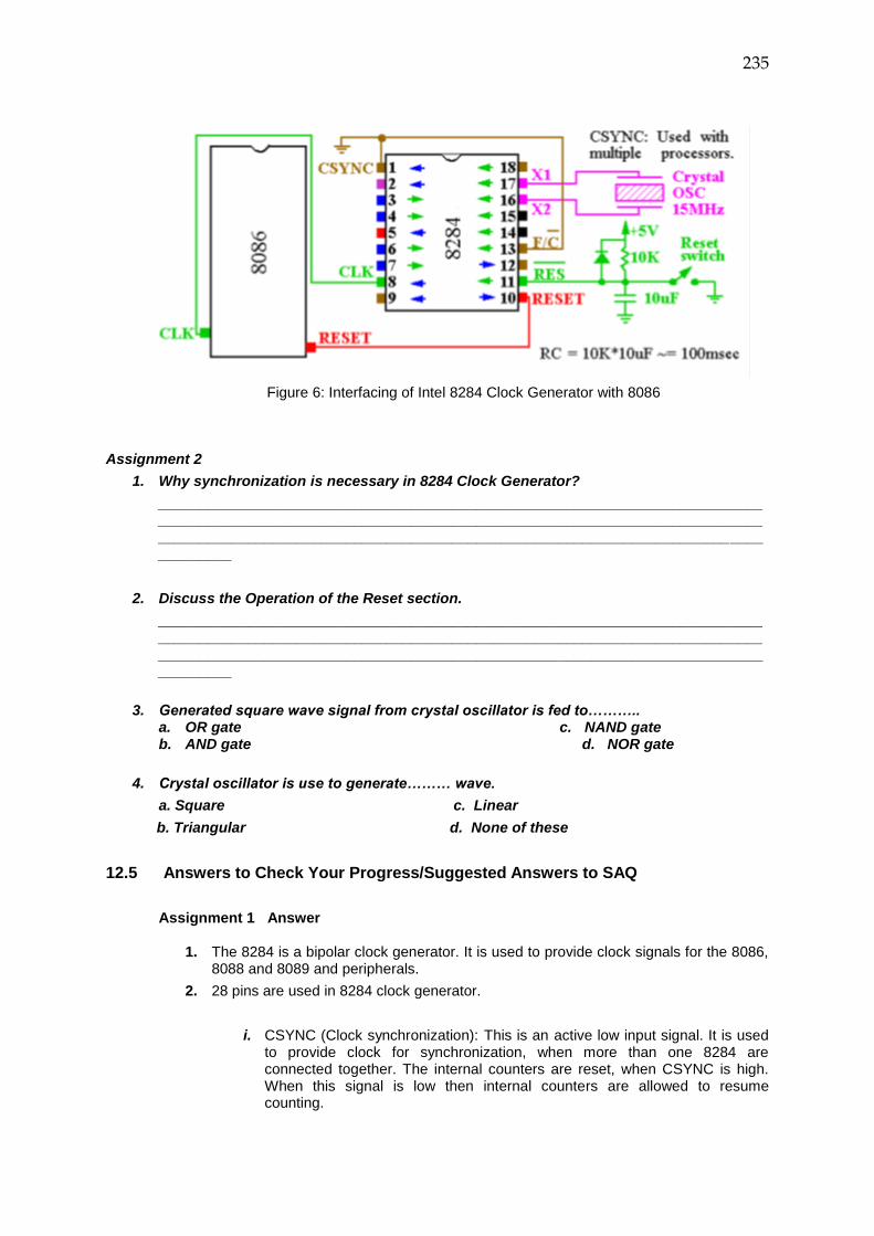
235
Figure 6: Interfacing of Intel 8284 Clock Generator with 8086
Assignment 2
1. Why synchronization is necessary in 8284 Clock Generator?
_______________________________________________________________________________________________________________________________________________________________________________________________________________________________________
2. Discuss the Operation of the Reset section.
_______________________________________________________________________________________________________________________________________________________________________________________________________________________________________
3. Generated square wave signal from crystal oscillator is fed to………..
a. OR gate c. NAND gate b. AND gate d. NOR gate
4. Crystal oscillator is use to generate……… wave.
a. Square c. Linear
b. Triangular d. None of these
12.5 Answers to Check Your Progress/Suggested Answers to SAQ
Assignment 1 Answer
1. The 8284 is a bipolar clock generator. It is used to provide clock signals for the 8086, 8088 and 8089 and peripherals.
2. 28 pins are used in 8284 clock generator.
i. CSYNC (Clock synchronization): This is an active low input signal. It is used to provide clock for synchronization, when more than one 8284 are connected together. The internal counters are reset, when CSYNC is high. When this signal is low then internal counters are allowed to resume counting.
236
ii. F/C (Frequency/Crystal select): The crystal oscillator or external source is used to generate clock in 8284. This pin is used to select an internal or external clock. Clock is generated by the 8284, if this pin is in low state and when this pin is high than external source will generate the clocks and applied through the EFI pin.
3. Ans. b
4. Ans. c
Assignment 2 Answer
1. Synchronization is required for providing RDY setup and hold times in all active asynchronous going edges. Inactive going edges signal of ready system does not required synchronization but for proper design of system hold time and RDY setup should be matched. Synchronization may be achieved by placing D-flip-flop between 8284 and RDY source and applying rising edge clock on the flip-flop CLK signal.
2. This section is used to provide the RESET signal to the micro processors on the every 1-to-0 transition of clock. The 8086/8088 microprocessors sample RESET at the 0-to 1transition of the clock, therefore this circuit achieves the timing requirements of the 8086/8088.
3. Ans. b 4. Ans. a
12.6 Bibliography/References/Suggested Readings: 1.Microprocessor Architecture, Programming and Applications with 8085, Ramesh. S. Gaonkar, Fourth Edition, Penram International Publishing. 2.Microprocessors And Applications, D.A.Godse, A.P.Godse, First Edition, technical Publications Pune.
12.7 Terminal and Model Questions
1.Draw the pin diagram of 8284 clock generator and explain each pin.
2. Draw the block diagram of Intel 8284 clock generator and explain it.
3. Explain the working of 8284 clock generator and its interfacing with microcontroller.
![Microprocessors and Microcontrollers Module 1 - 5[1]](https://static.cupdf.com/doc/110x72/577cdcba1a28ab9e78ab3fdd/microprocessors-and-microcontrollers-module-1-51.jpg)