Digital Communication 2 9/21/2010
Digital Communications2Lec1
(FALL 2010)
Asad AbbasAssistant Professor Telecom Department
Air University, IslamabadPakistan
9/21/2010 2
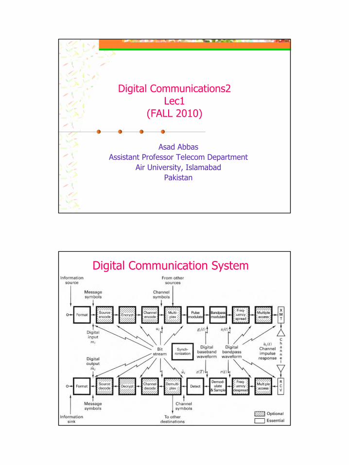
Digital Communication System

Digital Communication 2 9/21/2010
9/21/2010 3
Last Semester we talked about:
Formatting and Base band ModulationBaseband Demodulation and DetectionBand pass modulation and DemodulationCommunication Link Analysis
9/21/2010 4
We are going to talk about:
SynchronizationSynchronization TypesPhase Lock Loop
Digital Communication 2 9/21/2010
9/21/2010 5
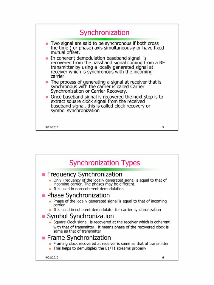
SynchronizationTwo signal are said to be synchronous if both cross the time ( or phase) axis simultaneously or have fixed mutual offset.In coherent demodulation baseband signal is recovered from the passband signal coming from a RF transmitter by using a locally generated signal at receiver which is synchronous with the incoming carrierThe process of generating a signal at receiver that is synchronous with the carrier is called Carrier Synchronization or Carrier Recovery.Once baseband signal is recovered the next step is to extract square clock signal from the received baseband signal, this is called clock recovery or symbol synchronization
9/21/2010 6
Synchronization Types
Frequency SynchronizationOnly Frequency of the locally generated signal is equal to that of incoming carrier. The phases may be different. It is used in non-coherent demodulation
Phase SynchronizationPhase of the locally generated signal is equal to that of incoming carrierIt is used in coherent demodulator for carrier synchronization
Symbol SynchronizationSquare Clock signal is recovered at the receiver which is coherent with that of transmitter. It means phase of the recovered clock is same as that of transmitter
Frame SynchronizationFraming clock recovered at receiver is same as that of transmitterThis helps to demultiplex the E1/T1 streams properly

Digital Communication 2 9/21/2010
9/21/2010 7
Coherent Receiver Vs. Non-coherent Receiver
Coherent Receiver requires, Phase and symbol synchronizationsNon-Coherent Receiver needs frequency synchronization ( in some techniques) but doesn’t need phase synchronization. However it requires symbol synch.
9/21/2010 8
How to Synchronies two signals?
It is done by using Phase Lock Loop (PLL)PLL is a feedback loop system in which the signal generated in PLL, the feedback signal, follows the input signal, the reference signal. When the two signals have same frequency and their phase difference is either zero or some fixed value, the PLL is said to be lockedDuring locked condition the Internal signal , a sinusoid, then represents a filtered version of the reference signal.

Digital Communication 2 9/21/2010
9/21/2010 9
PLL System
( )x t
Phase DetectorLoop Filter ( Low pass filter)Voltage Controlled Oscillator
(VCO)
( )y t
( )dv t ( )fv t
9/21/2010 10
Phase Lock Loop Applications
Carrier Recovery uses Phase SynchLocally generated signal is in phase with incoming carrier
Clock Recovery involves symbol SynchLocally generated clock is in phase with that of transmitter
Programmable Frequency SynthesisVariable frequency RF signal source
FM DemodulationFSK Demodulation
Digital Communication 2 9/21/2010
9/21/2010 11
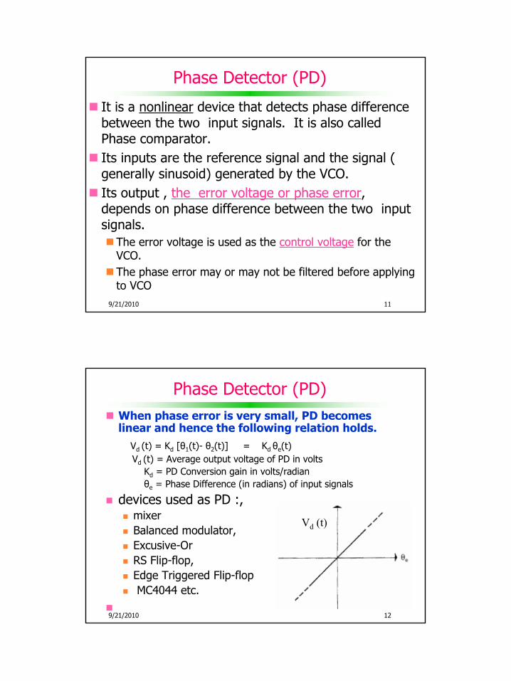
Phase Detector (PD)
It is a nonlinear device that detects phase difference between the two input signals. It is also called Phase comparator.Its inputs are the reference signal and the signal ( generally sinusoid) generated by the VCO. Its output , the error voltage or phase error, depends on phase difference between the two input signals.
The error voltage is used as the control voltage for the VCO. The phase error may or may not be filtered before applying to VCO
9/21/2010 12
Phase Detector (PD)When phase error is very small, PD becomes linear and hence the following relation holds.
Vd (t) = Kd [θ1(t)- θ2(t)] = Kd θe(t)Vd (t) = Average output voltage of PD in volts
Kd = PD Conversion gain in volts/radianθe = Phase Difference (in radians) of input signals
devices used as PD :, mixerBalanced modulator,Excusive-OrRS Flip-flop,Edge Triggered Flip-flop MC4044 etc.
Vd (t)

Digital Communication 2 9/21/2010
9/21/2010 13
Phase Detector Types
Analogue PDMixing Phase detector
Digital PDXOR Phase DetectorOver Driven Mixing Phase DetectorTwo State Phase Detector
9/21/2010 14
Mixing Phase Detector
Max Phase change between two maximum points = π
Reference Signal = sin (ωi t + θi(t)). VCO signal = cos (ωot + θo(t) ).
vd(t) = ½ Kd [ sin [(ωi + ωo)t + θi (t)+ θo(t)) + sin [(ωi − ωo)t + θi(t) − θo (t) ]
Sum term is rejected by the loop filter and hence it does not play any role. When PLL is locked then wo= wi
vd(t) = ½ Kd sin (θi(t) − θo (t) )= ½ Kd sin (θe(t) )= ½ Kd θe(t) if θe(t) is very samll
Digital Communication 2 9/21/2010
9/21/2010 15
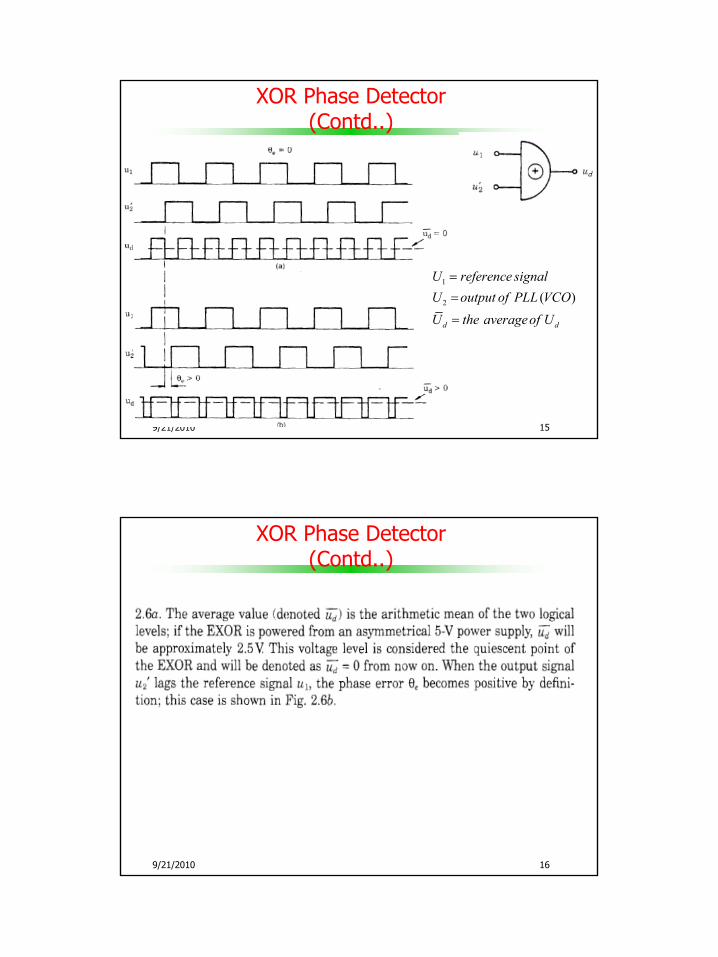
XOR Phase Detector(Contd..)
1
2 ( )
d d
U reference signalU output of PLL VCOU the averageof U
==
=
9/21/2010 16
XOR Phase Detector(Contd..)
Digital Communication 2 9/21/2010
9/21/2010 17
XOR Phase Detector(Contd..)
Average output of analog multiplier is sine of phase error whereas that of XOR is triangular function of phase error
If supply Voltage of XOR are UB and zero then
9/21/2010 18
XOR Phase Detector(Contd..)
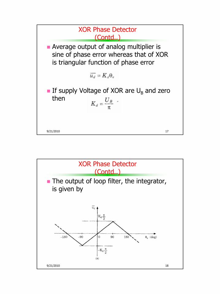
The output of loop filter, the integrator, is given by
Digital Communication 2 9/21/2010
9/21/2010 19
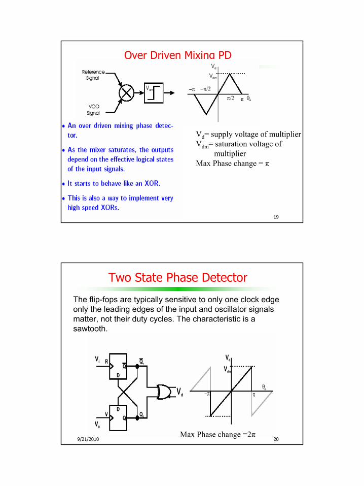
Over Driven Mixing PD
Vd= supply voltage of multiplierVdm= saturation voltage of
multiplierMax Phase change = π
9/21/2010 20
Two State Phase Detector
The flip-fops are typically sensitive to only one clock edgeonly the leading edges of the input and oscillator signals matter, not their duty cycles. The characteristic is a sawtooth.
Max Phase change =2π

Digital Communication 2 9/21/2010
9/21/2010 21
Loop FilterLoop Filter (LF)
It is a Low Pass filter. It removes any noise and high frequency components (sum signal) from the output voltage of phase detector and passes the difference signal thus giving an average (dc) voltage, called error voltage. The output of loop filter, Vf (t) which is almost equal to error voltage, forces the frequency of VCO to change in direction that reduces the frequency difference between input and VCO. It is the primary building block that determines dynamic performance of loop, which includes the following factors:
Capture and Lock RangeBandwidthTransient response
9/21/2010 22
Loop Filter..(2)
Simple RC Passive Lead-Lag
Active Lead-Lag Active PI

Digital Communication 2 9/21/2010
9/21/2010 23
Simple RC Loop Filter G(jw) = 1/(jwRC+ 1)
If w is large :G(jw) ~= 1/jwRC |G(jw)| ~= 1/wRClog(|G(jw)|) = log(1/wRC) = -log(wRC) = -log(w) - log(RC)Gaindb = 20 log10(|G(jw)|) = -20 log(w) - 20 log(RC)
Let w=wo ( > corner frequency) thenGain db (wo) = -20 log(wo) - 20 log(RC)
If w=10woGaindb(10wo) = -20 log(10wo) - 20 log(RC) Gaindb(10wo) - Gaindb(wo)= -20 db - in one decade!
Let w=2woGaindb(2wo) - Gaindb(wo) = -6.0206 db ~= -6db/octave.
If w is small:G(jw) ~= 1Gain db=0
9/21/2010 24
Simple RC Loop Filter G(jw) = 1/(jwRC+ 1)
If w = 1/RC, then GaindB= -3.02 dBPhase= - 45 degrees
2
2
2
1 1
20log ( )
20log1 20log ( ) 1
20log ( ) 11/ ( 1/ 2 )
20log ( / ) 1
tan ( ) tan ( / )
dB
cut off cut off
dB cut off
cut off
Gain G jw
wRC
wRCW RC f RC
Gain w W
Phase wRC w W
π− −
−
− −−
= − =
= − − +
= − +
= =
= − +
= − = −

Digital Communication 2 9/21/2010
9/21/2010 25
Simple RC Loop Filter Bode Plot
9/21/2010 26
Loop Filters Bode Plots
10log ωPassive Lead-lag Active Lead-lag
PI Filter
dB
( )F F w=
Digital Communication 2 9/21/2010
9/21/2010 27
Assignment-01
Find Transfer Functions of Passive lead-lag and Active lead-lag Loop filters
(points= 4)Find relations for cut-off (3 dB) frequencies for each of the filters given above
(Points=3)Draw bode Plot on logarithmic graph paper
(Points=3)Submission Date:
9/21/2010 28
Oscillator
It is an electronic device that generates different repetitive signals e.g. sine, square, rampIt has no input. It converts DC biasing current into AC. It is positive feedback system having the Close Loop Gain as 1<0. Some Types:
Hartley OscillatorColpitt OscillatorClapp oscillatorPhase Shift
Digital Communication 2 9/21/2010
9/21/2010 29
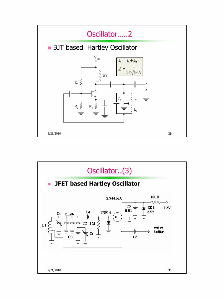
Oscillator…..2
BJT based Hartley Oscillator
9/21/2010 30
Oscillator..(3)
JFET based Hartley Oscillator

Digital Communication 2 9/21/2010
9/21/2010 31
Oscillator….4
Colpitt Oscillator
9/21/2010 32
Oscillators….5
Clapp Oscillator
Phase Shift Oscillator

Digital Communication 2 9/21/2010
9/21/2010 33
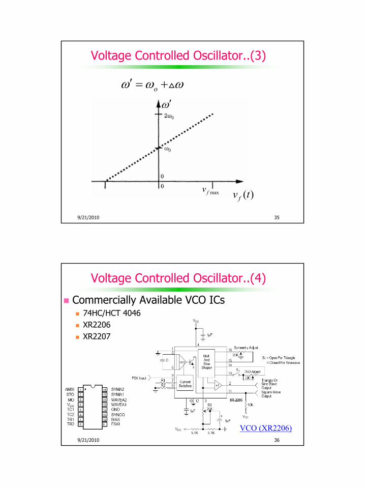
Voltage Controlled OscillatorThe VCO is an oscillator in which change in free-running frequency proportional to the input voltage.
The free-running frequency is the frequency of VCO when its input voltage is zero It is fixed by external resistor-capacitor network or inductor-capacitor network
Discreet VCO:
9/21/2010 34
Voltage Controlled Oscillator..(2)VCO Frequency = ∆ω= change in free running frequency of VCO caused by input voltage
Let ωfree-running = ωo
Change in frequency = ∆ω = Ko vf(t)Ko = VCO conversion Gain (radian/sec/volts)
vf (t)= output of LF= Input signal to VCO
( )( )0
( ) ( )
( ) cos( ( )) cos ( )
cos ( )
o o f
o o f
o
VCO Phase t dt w t k v t dt
VCO output y t t w t k v t dt
w t t
θ ω
θ
θ
′= = = +
= = = +
= +
∫ ∫∫
free runningω ω ω−′ = +
oω ω ω′ = +
Digital Communication 2 9/21/2010
9/21/2010 35
Voltage Controlled Oscillator..(3)
ω′
maxfv ( )fv t
ω′oω ω ω′ = +
9/21/2010 36
Voltage Controlled Oscillator..(4)
Commercially Available VCO ICs74HC/HCT 4046XR2206XR2207
VCO (XR2206)
Digital Communication 2 9/21/2010
9/21/2010 37
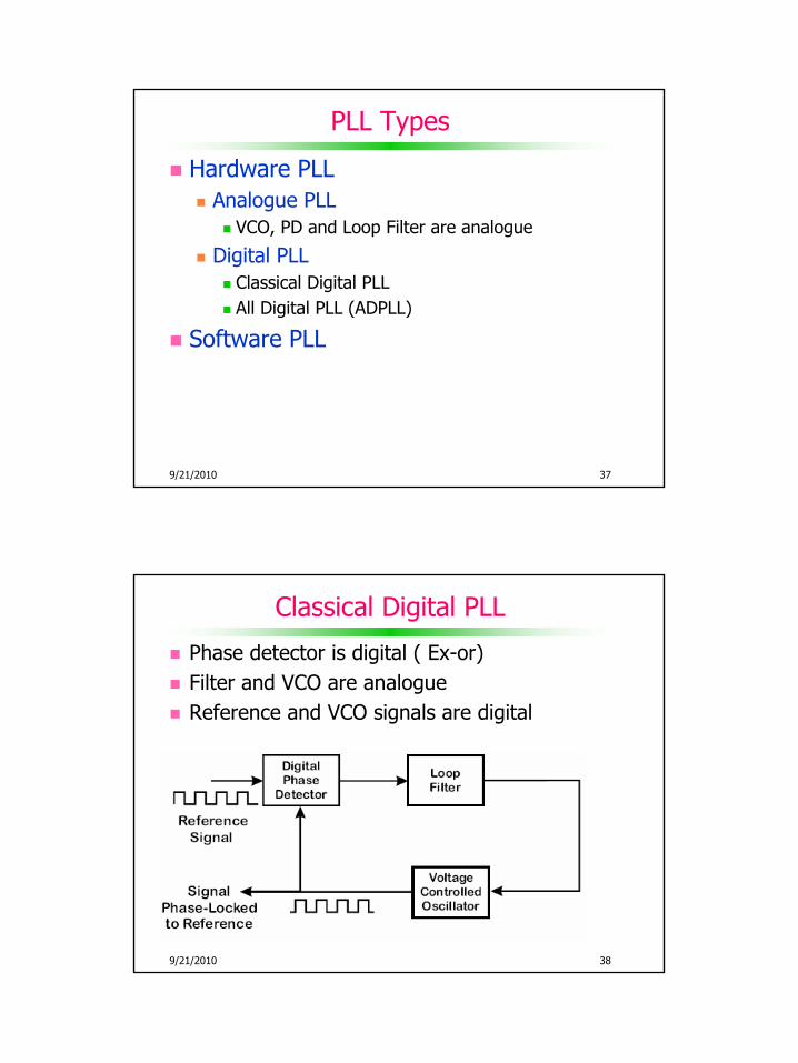
PLL Types
Hardware PLLAnalogue PLL
VCO, PD and Loop Filter are analogue
Digital PLLClassical Digital PLL All Digital PLL (ADPLL)
Software PLL
9/21/2010 38
Classical Digital PLL
Phase detector is digital ( Ex-or)Filter and VCO are analogueReference and VCO signals are digital
Digital Communication 2 9/21/2010
9/21/2010 39
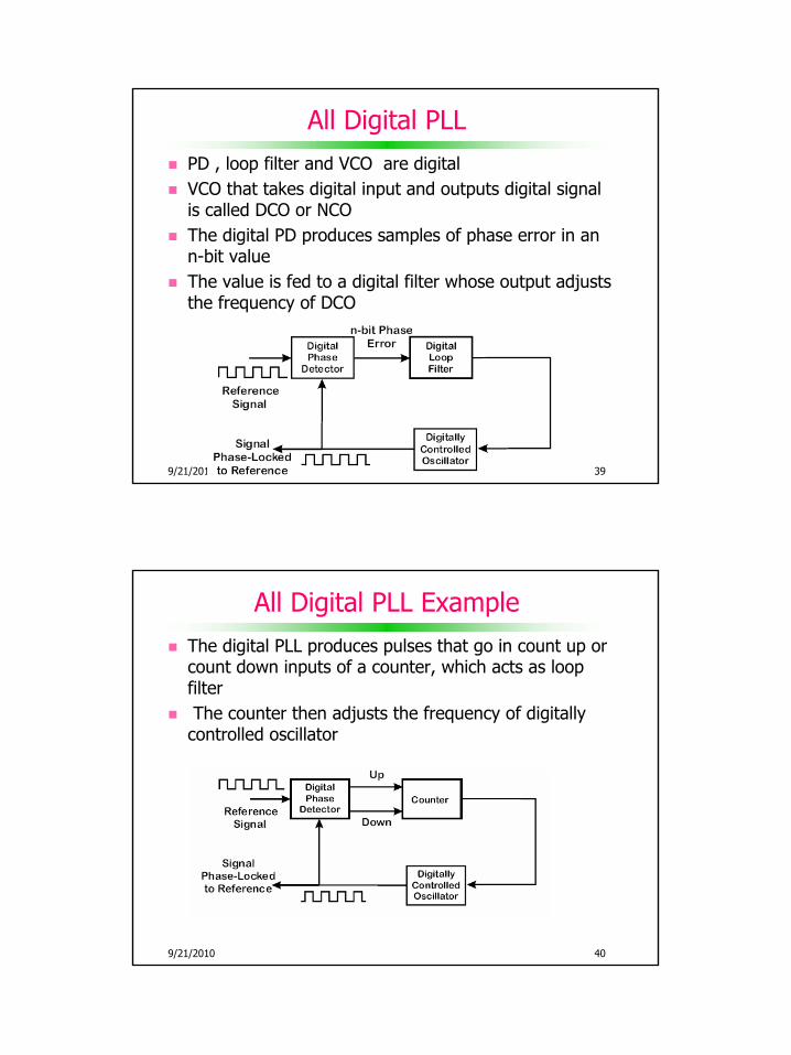
All Digital PLLPD , loop filter and VCO are digitalVCO that takes digital input and outputs digital signal is called DCO or NCOThe digital PD produces samples of phase error in an n-bit valueThe value is fed to a digital filter whose output adjusts the frequency of DCO
9/21/2010 40
All Digital PLL ExampleThe digital PLL produces pulses that go in count up or count down inputs of a counter, which acts as loop filter The counter then adjusts the frequency of digitally
controlled oscillator

Digital Communication 2 9/21/2010
9/21/2010 41
Software PLL (SPLL)It is implemented through software using microcontrollers or Digital Signal Processors
9/21/2010 42
Commercial PLL ICs
NE565NE5644046 (DPLL)

Digital Communication 2 9/21/2010
9/21/2010 43
NE564
9/21/2010 44
NE564..(2)
VCO frequency as a function of input voltage
Digital Communication 2 9/21/2010
9/21/2010 45
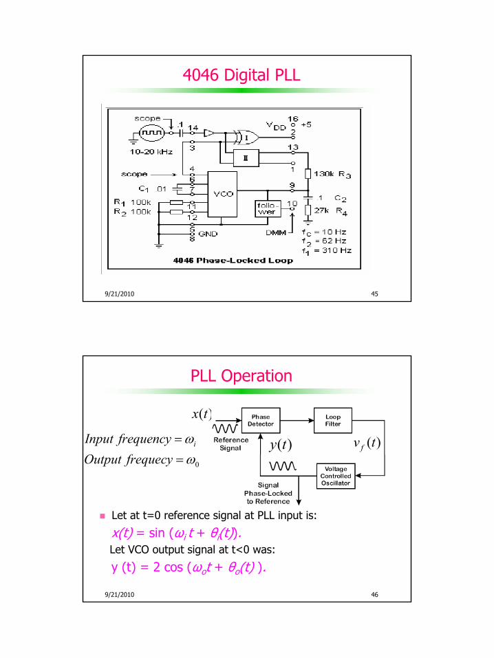
4046 Digital PLL
9/21/2010 46
PLL Operation
Let at t=0 reference signal at PLL input is:
x(t) = sin (ωi t + θi(t)).Let VCO output signal at t<0 was:
y (t) = 2 cos (ωot + θo(t) ).
( )dv t( )x t
0
iInput frequencyOutput frequecy
ωω
==
( )fv t( )y t
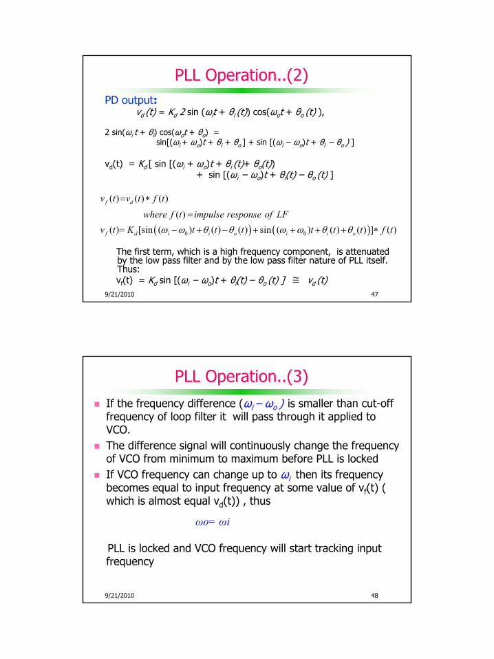
Digital Communication 2 9/21/2010
9/21/2010 47
PLL Operation..(2)PD output:
vd (t) = Kd 2 sin (ωit + θi (t)) cos(ωot + θo (t) ),
2 sin(ωi t + θi) cos(ωot + θo) = sin[(ωi + ωo)t + θi + θo ] + sin [(ωi− ωo)t + θi − θo ) ]
vd(t) = Kd [ sin [(ωi + ωo)t + θi (t)+ θo(t)) + sin [(ωi − ωo)t + θi(t)− θo (t) ]
The first term, which is a high frequency component, is attenuated by the low pass filter and by the low pass filter nature of PLL itself. Thus:vf(t) = Kd sin [(ωi − ωo)t + θi(t)− θo (t) ] vd (t)
( ) ( )0 0
( ) ( ) ( )
( )( ) [sin ( ) ( ) ( ) sin ( ) ( ) ( ) ] ( )
f d
f d i i o i i o
v t v t f t
where f t impulse response of LFv t K t t t t t t f tω ω θ θ ω ω θ θ
= ∗
=
= − + − + + + + ∗
≅
9/21/2010 48
PLL Operation..(3)If the frequency difference (ωi – ωo ) is smaller than cut-off frequency of loop filter it will pass through it applied to VCO. The difference signal will continuously change the frequency of VCO from minimum to maximum before PLL is locked If VCO frequency can change up to ωi then its frequency becomes equal to input frequency at some value of vf(t) ( which is almost equal vd(t)) , thus
PLL is locked and VCO frequency will start tracking input frequency
ωo= ωi

Digital Communication 2 9/21/2010
9/21/2010 49
PLL Operation…(4)
( ) ( )( )
;( ) [sin ( ) ( ) sin 2 ( ) ( ) ] ( )
( ) sin ( ) ( )
( ) ( ) ( )
o i
f d i o i i o
f d i o
o o f
At locked conditionv t K t t t t t f t
v t K t t
dw t t K v tdt
ω ωθ θ ω θ θ
θ θ
θ
=
= − + + + ∗
−
= =
( ) ( )f t F w⇔( )x t
( )y t( )fv t( )dv t
( VCO frequency depends on feedback voltage)
9/21/2010 50
Non-Linear Circuit ModelPLL equivalent circuit applicable for large Error ( non-linear analysis) when PLL is locked.
vd (t) = Kd sin( θi(t) - θo(t) )
( )i tθ
( )o tθ
0
t
oK ∫
( )f t
( ) ( )f t F w⇔
( ) ( )
( ) ( )
t
o o fo
do o fdt
t K v t dt
t w K v t
θ
θ
=
= =
∫
( )fv t
f(t)= Impulse response of Loop filter

Digital Communication 2 9/21/2010
9/21/2010 51
Linear Circuit ModelIt is used in linear analysis when PLL is locked and error is very small.For small phase error:
( )i tθ
0 ( )tθ
( )f t( )d eK tθ
( ) ( ) ( )e i oPhase error t t tθ θ θ= = −sin ( ) ( )e et tθ θ≅
( ) ( )
( ) ( )
t
o o fo
do o fdt
t K v t dt
t w K v t
θ
θ
=
= =
∫
0
t
oK ∫
( ) ( )f t F w⇔
( )fv t
9/21/2010 52
Closed Loop Transfer Function(using Linear model)
( )
( )
( )
( ) ( ) ( ) * ( )
( ) ( ),( ) ( ) ( ) * ( )
( ) ( ) ( ) ( )( ) ( ) ( ) ( ) ( )
( ) ( ) ( )( ) ( )
o f o d e
dodt
do o d i odt
o o d i o
o o d o o d i
o o d
i o d
w t K v t K K t f t
w t t sot K K t t f t
Taking FTjw w K K w w F wjw w K K w F w K K w F w
w K K F w H ww jw K K F w
θ
θ
θ θ θ
θ θ θθ θ θ
θθ
= =
=
= −
= −
+ =
= =+
Digital Communication 2 9/21/2010
9/21/2010 53
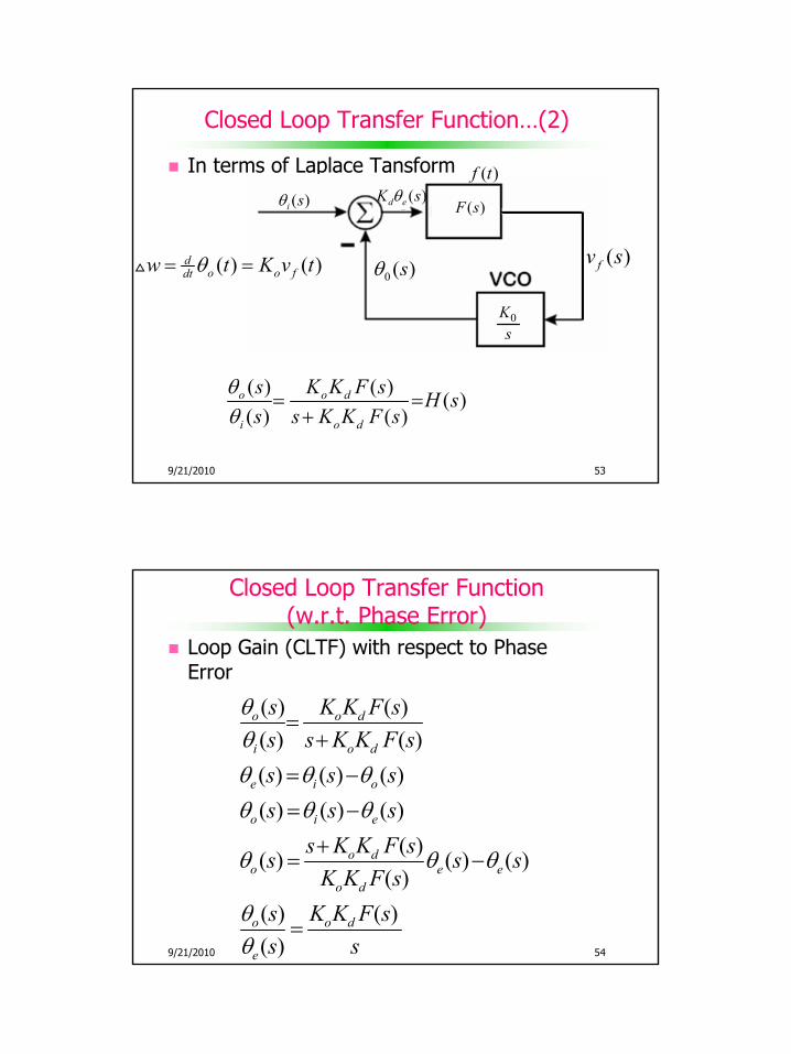
Closed Loop Transfer Function…(2)
In terms of Laplace Tansform
( ) ( ) ( )( ) ( )
o o d
i o d
s K K F s H ss s K K F s
θθ
= =+
0 ( )sθ
( )F s( )d eK sθ
( ) ( )do o fdtw t K v tθ= =
( )f t
0Ks
( )i sθ
( )fv s
9/21/2010 54
Closed Loop Transfer Function(w.r.t. Phase Error)
Loop Gain (CLTF) with respect to Phase Error
( ) ( )( ) ( )( ) ( ) ( )( ) ( ) ( )
( )( ) ( ) ( )( )
( ) ( )( )
o o d
i o d
e i o
o i e
o do e e
o d
o o d
e
s K K F ss s K K F ss s ss s s
s K K F ss s sK K F s
s K K F ss s
θθθ θ θθ θ θ
θ θ θ
θθ
=+
= −= −
+= −
=

Digital Communication 2 9/21/2010
9/21/2010 55
Closed Loop Transfer Function(Using All Pass Filter)
All Pass Loop FilterIt means F (w)=1. It happens when loop filter is removed and PLL consists of only PD and VCO
( ) ( )( )( ) ( )
o o d
i o d
o d
o d
w K K F wH ww jw K K F w
K Kjw K K
θθ
= = =+
=+
1st order Loop
9/21/2010 56
Closed Loop Transfer Function(using Simple RC Loop filter)
Simple 1st order RC Loop filter
1 1 1
1 11 1
1
1
1 1
0 12
1 0 1
0 12
1 0 1
1( )1
3
1( )1
( ): ( )( )
( )( )( ) ( )
( )
R C
o d
o d
o d d
o d d
d
d
F wjw R C
dB frequency w
wF wjw w jw
K K F wPutting in H wjw K K F w
K K F w K KH wjw K K F w jw jw K K
In terms of LTK KH s
s s K K
τ
τ
ττ τ
ττ τ
=+
= = =
= =+ +
=+
= =+ + +
=+ +
2nd order Loop

Digital Communication 2 9/21/2010
9/21/2010 57
Closed Loop Transfer Function(using Lead-Lag filter )
Loop Gain with 1st order Passive Lead-Lag Loop Filter
12 1
11 2 1
2 1
1 1 2
2 2 1 1 1 1
2
1 2
2
1 2
( )( )
1( )( ) 1
,1( )
1 ( )
1( )1 ( )
jwC
jwC
RLoopFilterTF F w
R R
jwR CF wjwC R R
R C R CjwF w
jwIn terms of LT
sF ss
τ ττ
τ τ
ττ τ
+= =
+ +
+=
+ += =
+=
+ +
+=
+ +
2nd order Loop
9/21/2010 58
Closed Loop Transfer Function(contd..)
2
21 22
2 1 2 2
1 2
2 2 1 22
1 2 2
( )( )( )
1(1 )1 ( )
1 ( ) ( )1 ( )(1 ) (1 ) ( )
( ) ( ) (1 ) ( )
o d
o d
o do d
o d o do d
o d o d
o d o d
Putting in the followingK K F wH w
jw K K F wjwK K
K K jwjwjw jw jw jw K K K Kjw K K
jwK K jw K K jw
jw jw K K K K jw
τττ τ
τ τ τ ττ ττ τ τ τ
τ τ τ
=+
+++ +
= =+ + + + ++
+ ++ + +
= =+ + + + 2
2 1 2 1 2
2 1 22
2 1 2 1 2
(1 ) ( ) ( )
(1 ) ( )( )(1 ) ( ) ( )
o d o d
o d
o d o d
jw K K K KIn terms of Laplace Transform
K K sH ss s K K K K
τ τ τ τ τ
τ τ ττ τ τ τ τ
+ + + + +
+ +=
+ + + + +
Loop Gain with Passive Lead-Lag Loop Filter

Digital Communication 2 9/21/2010
9/21/2010 59
Second order System
Transfer Function of a second ordered system is :
2
2 2( )2
n
n n
n
H ss s
natural frequencyDamping factor
ωζω ω
ωζ
=+ +
==
9/21/2010 60
Bode Plot of a General Second order System (Amplitude Response)
ωn = 2 π fn
( )H ω

Digital Communication 2 9/21/2010
9/21/2010 61
Bode Plot of General Second Ordered System (Phase Response)
( )H ω∠
9/21/2010 62
Second Order System ParametersNatural Frequency (wn)
It is frequency at which frequency response ( H(w) vs w plot) curve peaks (or is at it maximum value) for given value of damping factor When a signal ( phase or frequency change in the form of step or ramp) is applied to PLL its transient response oscillates around the steady state value for a while before achieving it. The of frequency of oscillation depends on damping factor. The frequency of oscillation when damping factor is zero is called natural frequency It determines the bandwidth of PLL
Damping Factor ( ζ )It is ability of the loop to controls the amount of overshoot orpeak of frequency response at natural frequency as a result of input frequency step.It controls how long the system will oscillates before attainingsteady state value during any transient responseIt also affects the bandwidth of PLL

Digital Communication 2 9/21/2010
9/21/2010 63
Natural Frequency and Damping Factor of PLL
Simple Loop filterComparing Denominator of PLL TF with that of the second order system we get:
12
12
1 1
1 1
1 12
o dn
o d
K KNatural frequencyR C
Damping factorR C K K
ω
ζ
= =
= =
9/21/2010 64
Natural Frequency and Damping Factor of PLL…. (2)
Lead-lag Filter
( )
( )
1 12 2
12
12
1 2 1 2 1
21 2 1
21 2
2
( ) ( )
1 1 12 ( )
1 1 12 ( )
2
o d o dn
o do d
o do d
n
K K K KNatural frequencyR R C
Damping factor R CK KR R C K K
K KK K
ωτ τ
ζ
ζ ττ τ
ω τ
= = = + +
= = + +
= + +

Digital Communication 2 9/21/2010
9/21/2010 65
PLL Design Advantage in using Lead-Lag filter
9/21/2010 66
Second-ordered PLL Bode Plot ( frequency response)

Digital Communication 2 9/21/2010
9/21/2010 67
Salient Features of Second-ordered PLL Bode Plot
It is low pass filterThe spectrum is flat (at DF=6) up to natural frequencyIt passes input phase signals having spectrum ( bandwidth) less than the natural frequency.
It means that a second ordered PLL is able to track phase and frequency modulation that lie within the band.
3-dB Bandwidth of the loop is given by:
9/21/2010 68
Transient Response of PLLWhen an under damped second order system encounters a sudden change at input, such as PLL input signal shifting from one frequency f1 to the other f2 in the form of step or ramp, the output of VCO tries to follow this change but oscillates about the frequency f2 for a time and eventually settles out at the new frequency (i.e. the steady state)The time required by PLL to achieve steady state value after a step is applied at its input is the settling time. The higher the damping factor lower the settling time.

Digital Communication 2 9/21/2010
9/21/2010 69
Normalized Transient Response of PLL
With passive RC Filter and passive lead lag filters as Loop filters
( )( )
( )( )
o
i
o
i
OutputPhase tInput Phase t
tNormalized Output Phaset
θθ
θθ
=
=
=
9/21/2010 70
Normalized Transient Response of Loop (contd..)
With Integrator as Loop Filter
( )( )
( )( )
o
i
o
i
Output Phase tInput Phase t
tNormalized Output Phaset
θθ
θθ
=
=
=

Digital Communication 2 9/21/2010
9/21/2010 71
Transient Response Parameters
Settling Time:Time required for the transient response to reach and remain within the specified percentage of the steady state value (e.g. 10%)Over shoot:It is maximum difference between the transient and the steady state value for a sudden change applied to PLL input
9/21/2010 72
PLL Parameters

Digital Communication 2 9/21/2010
9/21/2010 73
PLL ParametersFree-running Frequency (wo)
This is the frequency at which loop VCO operates when PLL is not locked or its input is zero. This frequency is determined by thecapacitive resistive network of the oscillator
DC LOOP Gain: DC Loop Gain=Kv = Ko Kd F(0) If F(0) = 1, then
Kv = Ko KdUnit of Kv = (sec)-1
Lock Time (tL ):The transient time required for free running loop to lock.
9/21/2010 74
PLL Parameters..(2)Hold (or Lock) Range:
The frequency range of reference signal in which the PLL is able to maintain phase tracking or the frequency range over which the loop system will follow changes in the input frequency during locked condition.It is centered at free-running frequency. The minima of this range is less and maxima is higher than free-running frequency.
Hold (or Lock) Range = 2 ωH = ωL1-ωL2
Hold-in (or Lock-in or Tracking ) Range It is how far the input frequency can deviate from the VCO free-running frequency and is numerically one-half the Hold, or lock range.
ωH = ωL = KoKd= ωL2-ωo=ωo- ωL1
Digital Communication 2 9/21/2010
9/21/2010 75
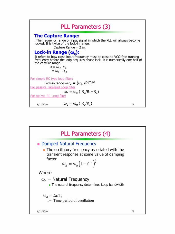
PLL Parameters (3)The Capture Range:The frequency range of input signal in which the PLL will always become
locked. It is twice of the lock-in range.Capture Range = 2 ωc
Lock-in Range (ωc):It refers to how close input frequency must be close to VCO free running frequency before the loop acquires phase lock. It is numerically one-half of the capture range.
ωc= ωc2- ω0= ω0 – ωc1
For simple RC type loop filter:Lock-in range =ωc = (ωH /RC)1/2
For passive lag-lead Loop filterωc = ωH ( R2/R1+R2)
For Active PI Loop filter
ωc = ωH ( R2/R1)
9/21/2010 76
PLL Parameters (4)
Damped Natural FrequencyThe oscillatory frequency associated with the transient response at some value of damping factor
Whereωn = Natural Frequency
The natural frequency determines Loop bandwidth
( )1221d nω ω ζ= −
ωd = 2π/T, T= Time period of oscillation

Digital Communication 2 9/21/2010
9/21/2010 77
Steady State Phase Error Reponse
It is the transient Response when PLL is in locked stateIt is the measure of the final value of phase error ( or difference voltage) after transients, generated as a result of Phase step, Frequency Step or Frequency ramp signal at PLL input, have died away.
9/21/2010 78
Steady State Error Response..(2)The Phase error generated when phase of the input signal to PLL changes abruptly is given by:
[ ]( )( )
( ) ( ( ) ( )( ) ( ( ) ( ))
( ) ( )
( ) ( ) ( )[1 ( )] ( )
( )1 ( )( )
( )( )( )
e i o
e i o
i o
i i
i
o di
o d
ie
o d
t t tw t t
w w
w w H wH w w
K K F w wjw K K F w
jw wwjw K K F w
θ θ θθ θ θ
θ θ
θ θθ
θ
θθ
= −
= ℑ −
= −
= −
= −
= − +
=+
Digital Communication 2 9/21/2010
9/21/2010 79
Steady State Error Response..(3)
According to final Value Theorem the final value of phase error is given by:
0
2
0
0
2
0
lim ( ) lim ( )
( ) ( )lim( )
lim ( ) lim ( )
( ) ( )lim( )
t e jw e
ijw
o d
t d jw d
ijw d
o d
t jw w
jw wjw K K F w
v t jwV w
jw w Kjw K K F w
θ θ
θ
θ
→∞ →
→
→∞ →
→
=
=+
=
=+
9/21/2010 80
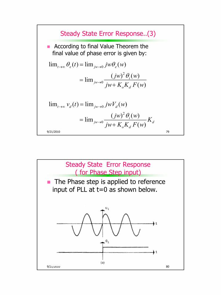
Steady State Error Response( for Phase Step input)
The Phase step is applied to reference input of PLL at t=0 as shown below.

Digital Communication 2 9/21/2010
9/21/2010 81
Steady State Error Response for Phase..(2)
Input Phase Step:
2
0
0
( ) ( )
( )
( ) ( ): lim ( ) lim( )
( )
lim ( ) lim 0( )
( ) ( ) 0( ) ( )
i
i
it e jw
o d
i
t e jwo d
i o
o i
Input phase step t u tTaking FT
wjw
jw wWe have tjw K K F w
Put value of wjwt
jw K K F wt tt t
No phaseerror in steady state irrespec
θ φ
φθ
θθ
θφθ
θ θθ θ
→∞ →
→∞ →
= =
=
=+
= =+
− ==
tive of the typeof loop filter
9/21/2010 82
Steady State Phase Error Response for Phase..(3)

Digital Communication 2 9/21/2010
9/21/2010 83
Steady State Phase Error Response (for frequency step input)
Input to PLL is a frequency step
9/21/2010 84
Steady State Phase Error Response for frequency…(2)
Input Frequency StepIf the input frequency changes suddenly from w1 to W2 then
2
2
0
0
( )( ) ( )
: ( )( )
( ) ( ): lim ( ) lim( )
( ),
lim ( ) lim( ) (0)
i
i
it e jw
o d
i
t e jwo d o d
Input frequency step wu tInput phase t w t u t
wTaking FT wjw
jw wWe have tjw K K F w
Putting the value of w we getw wt
jw K K F w K K F
Steady state
θ
θ
θθ
θ
θ
→∞ →
→∞ →
== =
=
=+
= =+
lim ( )(0)t e
o d
wphase error tK K F
θ→∞= =
Digital Communication 2 9/21/2010
9/21/2010 85
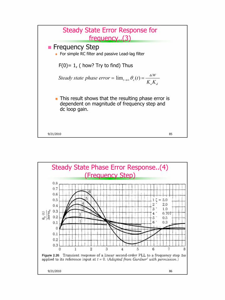
Steady State Error Response for frequency..(3)
Frequency Step For simple RC filter and passive Lead-lag filter
F(0)= 1, ( how? Try to find) Thus
This result shows that the resulting phase error is dependent on magnitude of frequency step and dc loop gain.
lim ( )t eo d
wSteady state phase error tK K
θ→∞= =
9/21/2010 86
Steady State Phase Error Response..(4)(Frequency Step)
Digital Communication 2 9/21/2010
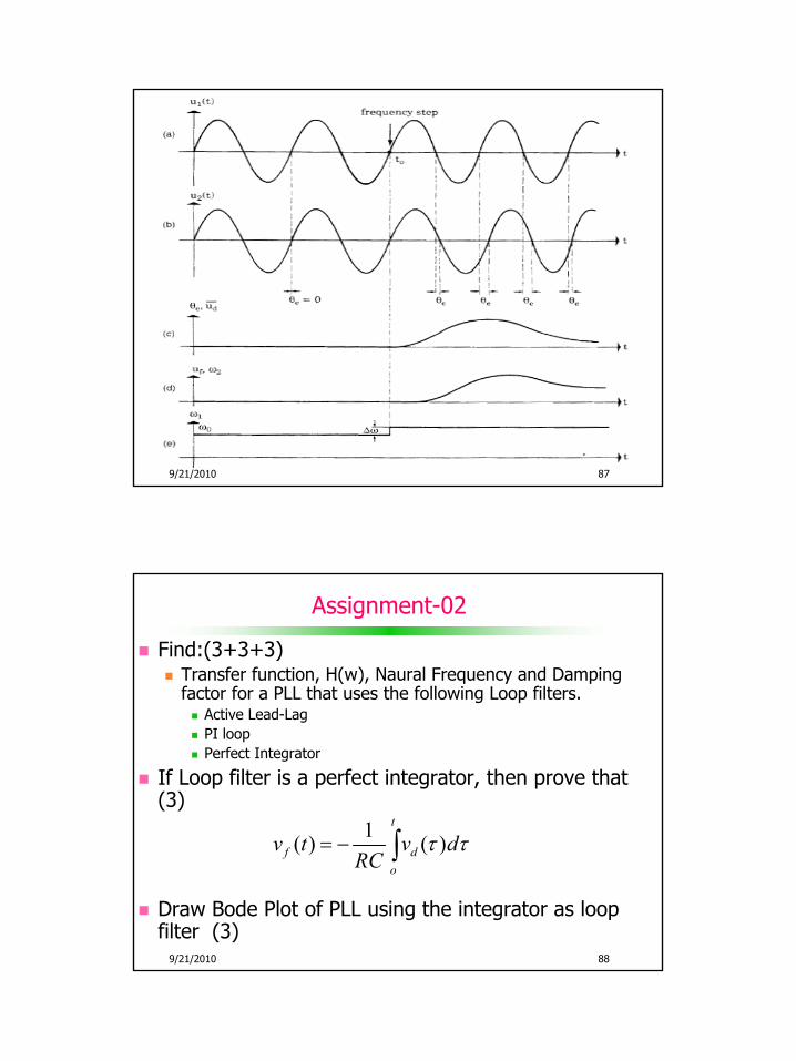
9/21/2010 87
9/21/2010 88
Assignment-02
Find:(3+3+3)Transfer function, H(w), Naural Frequency and Damping factor for a PLL that uses the following Loop filters.
Active Lead-Lag PI loop Perfect Integrator
If Loop filter is a perfect integrator, then prove that (3)
Draw Bode Plot of PLL using the integrator as loop filter (3)
1( ) ( )t
f do
v t v dRC
τ τ= − ∫

Digital Communication 2 9/21/2010
9/21/2010 89
Assignment-02
Frequency step is applied to a PLL that uses integrator as loop filter. Calculate the steady state phase error. (5)
If the input to a PLL is frequency ramp, shown at next slide, calculate its Steady State Phase Error if the PLL uses any of the loop filters given below (10):
Simple RCLead-lagPerfect integrator
9/21/2010 90
Assignment 2
Frequency ramp input.
Digital Communication 2 9/21/2010
9/21/2010 91
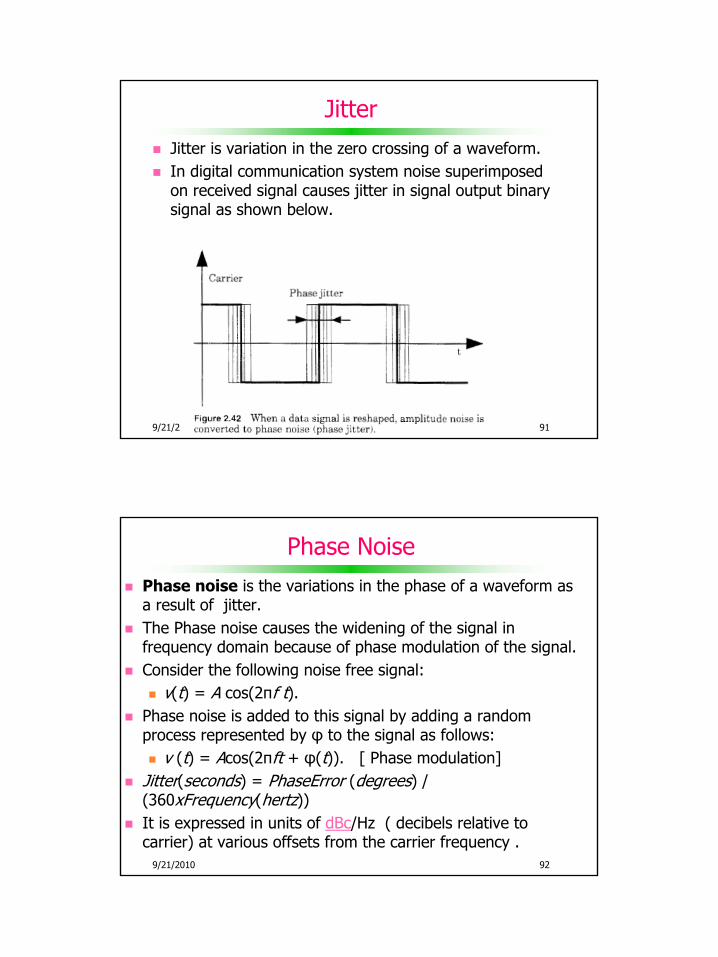
JitterJitter is variation in the zero crossing of a waveform.In digital communication system noise superimposed on received signal causes jitter in signal output binary signal as shown below.
9/21/2010 92
Phase NoisePhase noise is the variations in the phase of a waveform as a result of jitter. The Phase noise causes the widening of the signal in frequency domain because of phase modulation of the signal.Consider the following noise free signal:
v(t) = A cos(2πf t). Phase noise is added to this signal by adding a randomprocess represented by φ to the signal as follows:
v (t) = Acos(2πft + φ(t)). [ Phase modulation]Jitter(seconds) = PhaseError (degrees) / (360xFrequency(hertz))It is expressed in units of dBc/Hz ( decibels relative to carrier) at various offsets from the carrier frequency .

Digital Communication 2 9/21/2010
9/21/2010 93
PLL Performance in white Noise..(1)
VCO
sin[ ( )] ( )o iA t t n tω θ+ +
ˆcos[ ( )]oB t tω θ+( ) ( )f fv t n t+
ˆ( ) [ ( ) ( )]o f ft K v t n t dtθ = +∫
9/21/2010 94
PLL Performance in white Noise..(2)
ˆ VCO Output Phase due to noise Phase noiseθ = =
Single-sided Noise Power Spectral Density (PSD) = N0
Phase Variance = Noise Power (watts) =
White Noise double-sided PSD = G (w) = N0 /2 Watts/Hz
PSD of noise at PLL input =
PLL Phase noise PSD = PSD of Jitter in VCO signal
0( )G w N=
2( ) ( ) ( )( )
G w G w H wH w PLL Transfer Functionθ =
=

Digital Communication 2 9/21/2010
9/21/2010 95
PLL Performance in white Noise..(3)
1
Two sided PLL Loop (or Noise ) Bandwidth (in Hz) = WL
Single- Sided Loop Bandwidth ( or PLL Noise bandwidth) = BL (HZ)
Phase Variance (watts) =
Unit of ωn = radian/secUnit of BL= Hz
9/21/2010 96
PLL Loop (Noise ) Bandwidth
Single sided Loop BW=

Digital Communication 2 9/21/2010
9/21/2010 97
Non-Linear Loop Analysis
Linear Model of the Loop
9/21/2010 98
Non-Linear Loop Analysis..(2)
Non Linear Model of the Loop

Digital Communication 2 9/21/2010
9/21/2010 99
Non-linear Loop Analysis (contd..)For Kd =1
9/21/2010 100
Non-linear Loop Analysis (contd..)
Viterbi determined PDF of ϕ
= Normalized SNR
Digital Communication 2 9/21/2010
9/21/2010 101
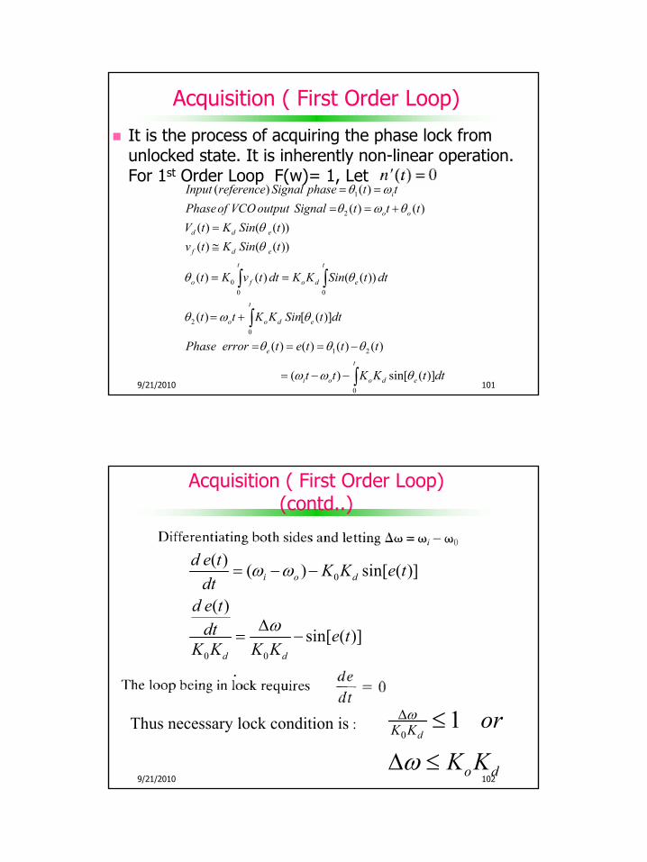
Acquisition ( First Order Loop)
It is the process of acquiring the phase lock from unlocked state. It is inherently non-linear operation. For 1st Order Loop F(w)= 1, Let
1
2
00 0
20
( ) ( )( ) ( )
( ) ( ( ))( ) ( ( ))
( ) ( ) ( ( ))
( ) [ ( )]
( ) ( )
i
o o
d d e
f d e
t t
o f o d e
t
o o d e
e
Input reference Signal phase t tPhaseof VCO output Signal t t tV t K Sin tv t K Sin t
t K v t dt K K Sin t dt
t t K K Sin t dt
Phase error t e t
θ ωθ ω θ
θθ
θ θ
θ ω θ
θ
= =
= = +
=≅
= =
= +
= = =
∫ ∫
∫1 2
0
( ) ( )
( ) sin[ ( )]t
i o o d e
t t
t t K K t dt
θ θ
ω ω θ
−
= − − ∫
9/21/2010 102
Acquisition ( First Order Loop)(contd..)
Thus necessary lock condition is :
0
0 0
( ) ( ) sin[ ( )]
( )
sin[ ( )]
i o d
d d
d e t K K e tdt
d e tdt e t
K K K K
ω ω
ω
= − −
∆= −
01
dK K
o d
or
K K
ω
ω
∆ ≤
∆ ≤

Digital Communication 2 9/21/2010
9/21/2010 103
Acquisition…(2)
0
( )ddt
d
e tK K
0 0
( )
sin[ ( )]d d
d e tdt e t
K K K Kω∆
= −
0 dK Kω∆
9/21/2010 104
END 1st Part
Next Part ( from slides 101-111 ) is for self reading

Digital Communication 2 9/21/2010
9/21/2010 105
PLL Design Consideration
Loop Gain. It affects the phase error between the input signal and the voltage controlled oscillator for a given frequency shift of the input signal. It also determines the `hold-in range'' of the loop providing no components of the loop go into limiting or saturation. This is because the loop will remain in lock as long as the phase difference between the input and the VCO is less than 90 degrees. The higher the loop gain, the further the input can change in frequency before the 90 degrees phase error is reached.
9/21/2010 106
PLL Design Consideration..(2)
Natural Frequency. The bandwidth of the loop depends on natural frequency which is determined by the filter components R1, R2 and C1, and the loop gain.The selection of the bandwidth may be governed by several things:
Noise bandwidthmodulation rates if the loop is to be used as an FM demodulatorhold-in range.
Digital Communication 2 9/21/2010
9/21/2010 107
PLL Design Consideration..(3)
There are two conflicting requirements that will have an affect on loop bandwidth:
a) Loop bandwidth must be as narrow as possible to minimize output phase jitter due to external noise.
b) The loop bandwidth should be made as large as possible to minimize transient error due to signal modulation, output jitter due to internal oscillator (VCO) noise, and to obtain best tracking and acquisition properties.Optimum solution lies some where in between
FM is designed on the basis of b criterion given above
9/21/2010 108
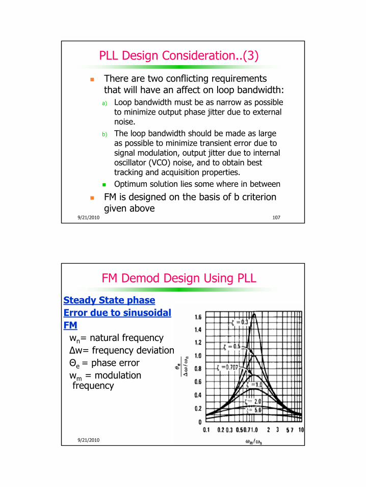
FM Demod Design Using PLL
Steady State phase Error due to sinusoidal FM
wn= natural frequency∆w= frequency deviationΘe = phase errorwm = modulation frequency

Digital Communication 2 9/21/2010
9/21/2010 109
FM Demod Design Using..(2)
It can be seen that the maximum phase error occurs when the modulating frequency Wm equals the loop natural frequency WnIf the loop has been designed with a damping factor of 0.707, the peak phase error (in radians) will be 0.71*
From this plot, it is possible to choose Wn for a given deviation and modulation frequency.
9/21/2010 110
Filter Time Constant VS natural Frequency
Lead-lag loop Filter
Filter Time Constant VS natural Frequency

Digital Communication 2 9/21/2010
9/21/2010 111
Damping Time Constant VS natural Frequency
Lead-lag loop Filter
Damping Time Constant VS natural Frequency
9/21/2010 112
FSK Demodulator Design Using PLL
If the loop is to demodulate frequency shift keying (FSK), it must follow step changes in frequency. The filter components must then be chosen in accordance with the transient phase error response for a frequency step It must be remembered that the loop filter must be wide enough so the loop will not lose lock when a step change in frequency occurs: the greater the frequency step, the wider the loop filter must be to maintain lock.

Digital Communication 2 9/21/2010
9/21/2010 113
FSK Demod Design ExampleMark frequency =2025 HzSpace frequency=2225 HzAs per FSK Demod Design curve (shown next) Peak Phase Error when Damping Factor is 0.707 is given by:
9/21/2010 114
FSK Demodulator Design..(2) Transient phase Error response of a second ordered PLL a frequency step ∆w applied to reference input at t=0

Digital Communication 2 9/21/2010
9/21/2010 115
FSK Demodulator Design…(3)
Calculate Loop filter time constants using either filter time constant versus natural frequency and damping vs. natural frequency curves or through natural frequency versus time constant relations derived earlier Calculate Noise bandwidth using noise bandwidth vs. damping curve or relation.
9/21/2010 116
END
Thanks