International Research Journal of Engineering and Technology (IRJET) e-ISSN: 2395 -0056
Volume: 02 Issue: 02 | June-2015 www.irjet.net p-ISSN: 2395-0072
© 2015, IRJET.NET- All Rights Reserved Page 501
POWER QUALITY ENHANCEMENT BY USING CASCADED H BRIDGE
MULTILEVEL INVERTER BASED DSTATCOM
S. B. Sakunde1, V. D. Bavdhane2
1 PG Student, 2Assistant Professor
Department of Electrical Engg,
Zeal education society’s DCOE, Narhe ,Pune, Maharashtra, India [email protected], [email protected]
--------------------------------------------------------------------***---------------------------------------------------------------------Abstract - In power system reactive power
compensation is important concern as V-Q profile are
interrelated. This paper emphasize on compensation of
reactive power and harmonics. The system with CHB
inverter is more robust and has less number of switches
which in turn reduces switching losses. In this paper
synchronous reference frame theory is used for
reference signal generation and capacitor DC voltage is
regulated by using PI controller. The gate pulses to
Inverter Bridge are given by LSPWM technique. In this
paper DTATCOM is designed for 11KV distribution
system by using CHB inverter for compensation of
reactive power and harmonics. The results are obtained
through MATLAB. Comparative analysis in terms of
THD is made for 3 and 5 level inverter.
Key Words: DSTATCOM, Synchronous reference frame
theory (SRF), level shifted pulse width modulation
(LSPWM), cascaded H bridge multilevel inverter (CHB)
1. INTRODUCTION
In modern power system power quality is very important
issue related to THD. For improving power quality in
terms of THD and compensating reactive power series or
shunt compensators are used. Simple or multilevel
inverter can be used for meeting these objectives. Simple
inverter produces only three voltages Levels while
multiple voltage levels can be achieved by using multilevel
inverter which produces less harmonic distortions [2]. By
increasing number of voltage levels of inverter output
waveform become more sinusoidal and which thus results
in reduced THD. Only the constraint is as number of
voltage levels of inverter are increased, the number of
bridges in series needs to be increased.
The multilevel inverter is categorized as cascaded H
Bridge, Diode clamped and Flying capacitor inverter [5].
The CHB inverters are mostly used due to their advantages
like simplicity, low switching losses and reduced number
of switches. The STATCOM used at distribution side is
known as DSTATCOM. By varying magnitude and phase
angle of inverter voltage reactive power can be exchanged.
2. DESIGN OF DSTATCOM
2.1 Principle of DSTATCOM
DSTATCOM is a shunt-connected custom power device
designed for power factor correction, current harmonics
filtering and load balancing. It can also be used for voltage
regulation at a distribution bus. It is often referred to as a
shunt or parallel active power filter. It consists of a voltage
or a current source PWM converter. It operates as a
current controlled voltage source and compensates
current harmonics by injecting the harmonic components
generated by the load but phase shifted by 180 degrees.
With an appropriate control scheme, the DSTATCOM can
also compensate for poor load power factor.
This paper focuses on DSTATCOM based on CHB inverter
where dc energy from renewable sources or batteries
converted into ac energy. Fig1 shows two level voltage
source converter with dc energy source is connected in
shunt to transmission line by using coupling transformer.
Three phase ac voltages are obtained from dc voltage
across storage device by using VSC. By varying magnitude
and phase angle of inverter voltage reactive power can be
exchanged between DSTATCOM and ac system. Such type
of arrangement provides voltage regulation, compensation
of reactive power, correction of power factor elimination
of current harmonics [1].

International Research Journal of Engineering and Technology (IRJET) e-ISSN: 2395 -0056
Volume: 02 Issue: 02 | June-2015 www.irjet.net p-ISSN: 2395-0072
© 2015, IRJET.NET- All Rights Reserved Page 502
Fig -1: Schematic diagram of DSTATCOM
2.2 Cascaded H Bridge multilevel inverter
Fig -2: Single Bridge inverter
The schematic diagram of simple bridge inverter is shown
in fig.2. The switching state of various switches is
presented in table- 1. The 1 and 0 represents off and on
state of switch respectively.
Table -1: Switching table for single bridge inverter
Voltage
level S1 S2 S3 S4
Vdc 1 1 0 0
0 0 1 0 1
-Vdc 0 0 1 1
Multilevel converters have types as diode clamped, flying
capacitor and cascaded multilevel inverter [2]. But the
CHB inverter is used mostly due to advantages like
simplicity, modularity, low switches and low switching
losses. Mostly IGBT switches are used to achieve high
switching efficiency.
With CHB inverter we get multiple voltage levels. The
levels of voltages depend basically on number of bridges
connected in series. The numbers of output voltage levels
of CHB are 2n+1, where n is number of H bridges
connected in series. Thus with single CHB inverter having
n=1, three levels of voltages are produced as +Vdc, 0 and –
Vdc. With two H-bridges connected in series as shown in
fig. 3, it produces five levels of output voltage as +2Vdc,
+Vdc, 0, -Vdc, -2Vdc. The switching order of various
switches under such configuration is mentioned in table-2.
Fig -3: Five level CHB inverter
Table -2: Switching table for 5 level CHB inverter
Voltage
level
S1 S2 S3 S4 S5 S6 S7 S8
2Vdc 1 1 0 0 1 1 0 0
Vdc 1 1 0 0 0 0 0 0
0 0 1 0 1 0 1 0 1
-Vdc 0 0 1 1 0 0 0 0
-2Vdc 0 0 1 1 0 0 1 1
International Research Journal of Engineering and Technology (IRJET) e-ISSN: 2395 -0056
Volume: 02 Issue: 02 | June-2015 www.irjet.net p-ISSN: 2395-0072
© 2015, IRJET.NET- All Rights Reserved Page 503
2.3 Reference signal generation for compensation
of harmonics by using SRF method
Fig -4: Reference signal generation In fig.4, entire reference current generation scheme has been illustrated. The load currents Ia, Ib and Ic are transformed to corresponding d-q axis currents Id and Iq. Iddc and Iqdc indicate fundamental frequency component of Id and Iq. The oscillating components are filtered out using low pass filter [9]. The active and reactive components of the 3Φ system are represented by the direct and quadrature components respectively. Also fundamental components are transformed into DC quantities which can be separated easily through filtering.
As shown in Fig.4. PI controllers are required for maintaining DC bus voltage constant and voltage regulation at PCC. In d-q-0 frame source currents are calculated as
id*=icd+_iddc
iq*=icq+_iqdc
Where Id* and Iq* are estimated dc components of active and reactive current component of reference source currents in dq frame. iddc and iqdc are dc components of active and reactive load current obtained using low pass filter. icd and icq are output of DC voltage controller and AC voltage controller outputs respectively. Isa*, Isb*, Isc* are reference source current which are obtained from inverse parks transformation of Id* and Iq*. Harmonic
current is obtained by subtracting reference currents Isa*, Isb* and Isc* from load currents Ia, Ib and Ic. This harmonic current is nothing but error signal. Error signal is compared with statcom current to give gate signal to inverter.
2.4 Level shifted PWM technique for gate signal
generation
CHB inverter is generally controlled using multicarrier
method like level shifted PWM or phase shifted PWM [8].
Level shifted PWM includes arrangements like Phase
Disposition or Phase Opposition Disposition or Alternative
Phase Opposition Disposition. This paper work represents
level shifted phase disposition PWM technique. The
numbers of carrier waveforms required are given by m-1,
where m is number of output voltage levels. So to produce
five output voltage levels four triangular carrier
waveforms with frequency 2 khz are chosen as shown in
Fig.5.
Fig -5: Level Shifted carrier PWM
Paragraph comes content here. Paragraph comes content here. Paragraph comes content here. Paragraph comes content here. Paragraph comes content here. Paragraph comes content here. Paragraph comes content here. Paragraph comes content here. Paragraph comes content here. Paragraph comes content here. Paragraph comes content here. Paragraph comes content here. Paragraph comes content here. Paragraph comes content here.

International Research Journal of Engineering and Technology (IRJET) e-ISSN: 2395 -0056
Volume: 02 Issue: 02 | June-2015 www.irjet.net p-ISSN: 2395-0072
© 2015, IRJET.NET- All Rights Reserved Page 504
3. MATLAB MODELING AND RESULTS
The system parameters considered for simulation study
are as follows
Table -3: System parameters System parameter
Rating
Source voltage 11 kV
Frequency 50Hz
DC bus capacitance 1550e-6F
Inverter series inductance 10 mH
Source resistance 0.1 ohm
Source inductance 0.9 mH
Load resistance 60 ohms
Load inductance 30mH
3.1 Results Obtained Without DSTATCOM
The Matlab model for basic power system without any
compensating device is shown in Fig.6.
Fig -6: Basic uncompensated power system under study with a nonlinear load
Fig.7 shows source voltage, current and load current
without DSTATCOM. It seems that load current and source
current both are same and non sinusoidal without
DSTATCOM.
Fig -7: Source voltage, current and load current without DSTATCOM
The harmonic spectrum of Phase-A source current without
DSTATCOM is presented in fig.8. The THD of source
current without DSTATCOM is observed as 28.25%.
Fig -8: Harmonic spectrum of Phase-A Source current
without DSTATCOM
3.2 Results Obtained with DSTATCOM
Simulink model of power system under study
compensated with multilevel CHB based inverter with
LSPWM using SRF based method is represented in fig.9.

International Research Journal of Engineering and Technology (IRJET) e-ISSN: 2395 -0056
Volume: 02 Issue: 02 | June-2015 www.irjet.net p-ISSN: 2395-0072
© 2015, IRJET.NET- All Rights Reserved Page 505
Fig -9: Simulink model of power system with DSTATCOM
3.2.1 Results of Three Level CHB inverter based
DSTATCOM
Phase A voltage of Three level LSPWM inverter is shown in
fig.10.
Fig -10: Three level output voltage of inverter
Under this case source voltage, current and load current
with three level CHB inverter with LSPWM based
DSTATCOM using SRF are shown in fig.11. With the help of
DSTATCOM source current becomes sinusoidal although
load current is non sinusoidal.
Fig -11: Source voltage, current and load current with three level CHB inverter with LSPWM based DSTATCOM using SRF
Harmonic spectrum analysis of Phase-A Source current
with three level CHB inverter with PSPWM based
DSTATCOM using SRF method is shown in fig.12. The THD
of source current with DSTATCOM is reduced to 4.73%.
Fig -12: Harmonic spectrum analysis of Phase-A Source current with three level CHB inverter with PSPWM based DSTATCOM using SRF
3.2.2 Results of Five Level CHB inverter based
DSTATCOM
The voltage of Phase A of Five level LSPWM inverter is
represented in fig. 13. It shows five step output.
International Research Journal of Engineering and Technology (IRJET) e-ISSN: 2395 -0056
Volume: 02 Issue: 02 | June-2015 www.irjet.net p-ISSN: 2395-0072
© 2015, IRJET.NET- All Rights Reserved Page 506
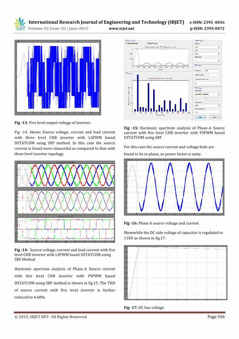
Fig -13: Five level output voltage of inverter.
Fig -14. Shows Source voltage, current and load current
with three level CHB inverter with LSPWM based
DSTATCOM using SRF method. In this case the source
current is found more sinusoidal as compared to that with
three level inverter topology.
Fig -14: Source voltage, current and load current with five level CHB inverter with LSPWM based DSTATCOM using SRF Method
Harmonic spectrum analysis of Phase-A Source current
with five level CHB inverter with PSPWM based
DSTATCOM using SRF method is shown in fig.15. The THD
of source current with five level inverter is further
reduced to 4.68%.
Fig -15: Harmonic spectrum analysis of Phase-A Source current with five level CHB inverter with PSPWM based DSTATCOM using SRF For this case the source current and voltage both are
found to be in phase, so power factor is unity.
Fig -16: Phase A source voltage and current
Meanwhile the DC side voltage of capacitor is regulated to
11KV as shown in fig.17.
Fig -17: DC bus voltage.

International Research Journal of Engineering and Technology (IRJET) e-ISSN: 2395 -0056
Volume: 02 Issue: 02 | June-2015 www.irjet.net p-ISSN: 2395-0072
© 2015, IRJET.NET- All Rights Reserved Page 507
A DSTATCOM with three level and five level CHB inverter
is investigated and comparison as follows-
Table -4: Comparison of three level and five level
multilevel inverter using LSPWM technique from
simulation results for non linear load for considered
power system.
Method Level % THD Fundamental
SRF Three 4.73 255.1
Five 4.65 254.9
4. CONCLUSION
In this paper comparison of three level and five level
multilevel inverter is presented. The reference current is
generated by using SRF method which considers abc to
dq0 transformation. DC bus voltage is regulated to 11KV
by using PI controller. The percentage of total harmonic
distortion is reduced with increase in inverter levels.
Further the system can be examined for seven level
topology.
REFERENCES
[1] J. Ganesh Prasad Reddy and K. Ramesh Reddy “Design and
Simulation of Cascaded H-Bridge Multilevel Inverter Based
DSTATCOM for Compensation of Reactive Power and
Harmonics,”1st Infl Conf. on Recent Advances in Information
Technology RAIT-2012
[2] J.S.Lai. and F.Z.Peng "Multilevel converters - A new bread of
converters, "IEEE Trans. Ind.Appli. • vo1.32. No.3. pp.S09-
S17. May/ Jun. 1996.
[3] P.Bhagwat. and V.R.Stefanovic. "Generalized structure of a
multilevel PWM Inverter:' IEEE Trans. Ind. Appln, VoI.IA-
19. no.6, pp. I OS7-1069, Nov.!Dec. 1983.
[4] J.Rodriguez. Jih-sheng Lai, and F Zheng peng, "Multilevel
Inverters; A Survey of Topologies, Controls, and
Applications," IEEE Trans. Ind. Electron., vol.49, n04.,
pp.724-738. Aug.2002.
[5] Roozbeh Naderi, and Abdolreza rahmati, "Phase-shifted
carrier PWM technique for general cascaded inverters," IEEE
Trans. Power.Electron., vo1.23, no.3, pp. I 257-I 269.
May.2008.
[6] Bhim Singh, Kamal AlHaddad & Ambrish Chandra, 1999, A
Review of Active Filter for Power Quality Improvements,
IEEE Trans on Industrial Electronics, 46(S), pp.960970
Mauricio Angulo, Pablo Lezana, Samir Kouro, Jos'e
Rodr'lguez and Bin Wu, "Level-shifted PWM for Cascaded
Multilevel Inverters with Even Power Distribution" IEEE
Power Electronics specialist conference, 17-21 June 2007,
pp.2373-2378.
[7] B. P. McGrath and D. G. Holmes, "Multicarrier PWM
strategies for multilevel inverters," IEEE Trans. Ind. Electron.,
vol. 49, no. 4, pp.858- 867, August 2002.
[8] Mr. Parmar Dipakkumar G and Mr. Kumar
Manoharjitsingh h,” Comprehensive review of to study about
power quality improvement in distribution network using
dstatcom,” International Journal For Technological Research
In Engineering Volume 2, Issue 6, February-2015


![REVIEW OF CONTROL STRATEGIES OF DSTATCOM · Fig. 2 Equivalent circuit of DSTATCOM The operation of DSTATCOM is explained in the following modes [2]: Mode 1: If V SHabc is in-phase](https://static.cupdf.com/doc/110x72/5ec37ced6f2e09596744a3b6/review-of-control-strategies-of-dstatcom-fig-2-equivalent-circuit-of-dstatcom-the.jpg)