


INVESTIGATIONS ON InSb PLASMONIC
DEVICES FOR SENSOR APPLICATIONS AT
TERAHERTZ FREQUENCIES
Thesis
Submitted in partial fulfilment of the requirements for the degree of
DOCTOR OF PHILOSOPHY
by
SHOURIE RANJANA J
(Reg.No. 100501PH10F01)
DEPARTMENT OF PHYSICS
NATIONAL INSTITUTE OF TECHNOLOGY KARNATAKA
SURATHKAL, MANGALORE – 575025
JULY 2017

INVESTIGATIONS ON InSb PLASMONIC
DEVICES FOR SENSOR APPLICATIONS AT
TERAHERTZ FREQUENCIES
Thesis
Submitted in partial fulfilment of the requirements for the degree of
DOCTOR OF PHILOSOPHY
by
SHOURIE RANJANA J
(Reg.No. 100501PH10F01)
Research Supervisors
Prof. G. Umesh
Dr. M. N. Satyanarayan
DEPARTMENT OF PHYSICS
NATIONAL INSTITUTE OF TECHNOLOGY KARNATAKA
SURATHKAL, MANGALORE – 575025
JULY 2017
D E C L A R A T I O N
By the Ph.D. Research Scholar
I hereby declare that the Research Thesis entitled “INVESTIGATIONS ON InSb
PLASMONIC DEVICES FOR SENSOR APPLICATIONS AT TERAHERTZ
FREQUENCIES” which is being submitted to the National Institute of Technology
Karnataka, Surathkal in partial fulfillment of the requirement for the award of the
Degree of Doctor of Philosophy in Physics, is a bonafide report of the research work
carried out by me. The material contained in this Research Thesis has not been submitted
to any University or Institute for the award of any degree.
Shourie Ranjana J
Reg: No 100501PH10F01
Department of Physics
Place: NITK Surathkal
Date:

C E R T I F I C A T E
This is to certify that the Research Thesis entitled “INVESTIGATIONS ON InSb
PLASMONIC DEVICES FOR SENSOR APPLICATIONS AT TERAHERTZ
FREQUENCIES” submitted by Shourie Ranjana J (Reg.No: 100501PH10F01) as the
record of the research work carried out by her, is accepted as the Research Thesis
submission in partial fulfillment of the requirements for the award of degree of Doctor of
Philosophy.
Research Guides
G. Umesh M.N. Satyanarayan
Chariman - DRPC

Acknowledgements
Acknowledgements
If I am what I am today, it was all due to such unlimited cooperation and encouraging
supports that was showered on me day in day out. Hence I stand with a responsibility to
express my overflowing sentiments of gratitude.
I express my sincere thanks to my supervisors Prof. G. Umesh and Dr. M. N. Satyanarayan.
They had offered their expert guidance and support that were essential to successfully
complete my PhD. I was able to gain valuable life experiences from each interaction that I
had with each of them. As teachers, they had enabled me to open the book of knowledge and
spot out many aspects of my research activities. As human persons, they had offered me
constant motivation and guidance. I’m very grateful to each of them for the dedicated
support and encouragement they had rendered to me.
I thank the Director, Dean of Academic Affairs, and Dean – Research and Consultancy and
the Department of Physics for their supports and guidance given all through my stay at
NITK. I gratefully remember and say ‘Thank You’ for awarding me the full time Institute
Research Scholarship.
With a grateful heart, I thank Prof. H.D. Shashikala - Head, Department of Physics and
Chairman, Prof. G. K. Shivakumar Department of Physics and Prof. Sripati Department of
Electronics and Communication Engineering, Members of the RPAC Committee. They had
spent their precious time, attending my seminars, evaluating my work and provided me
valuable suggestions during each of those discussions that I had with them.
I thank Prof. Kasturi V. Bangera, Prof. N.K. Udayashankar, Dr. H.S. Nagaraja, Dr. Ajith
K.M for offering me moral support and best wishes.
I express my thanks to Dr. K.B. Manjunath, Dr.Vikas M. Shelar, Mr. Hidayath Ulla, Ms.
Jean Maria Fernandes, Mr. Ravindra Kiran, Mr. Nimith, Mr. Achutha, Mr. Mahesh for their
cooperation and support. I thank Mr. Shashidhara for extending his support during my initial
experimental works at NITK.

Acknowledgements
I extend my sincere thanks Mr.M.Chandranath, Mr.Sheshappa Naik, Mrs. Sarita Shetty, Ms.
Usha, Mrs. Ashalatha, Mr. Dhanaraj and Mrs.Mohini Department of Physics for
administrative assistance.
My sincere and heartfelt thanks to Dr S.S. Prabhu, Department of Condensed Matter Physics,
TIFR – Mumbai for his generous support, immense guidance in helping me to use his lab
facility. I as well thank his research students, Dr. Reddy, Mr. Harshad, Mr. Prathamesh and
Mr. Abishek for being generous and supportive in helping me carry out my experiments.
I offer my sincere thanks to Dr. Nageshwari IITBNF, IITB Mumbai for offering her full
support during my INUP Projects. I thank Mr. Rajaram and Mr. Aravind who had helped me
to fabricate the devices by Laser Micromachining in Mumbai.
I say a very special thanks to Mr. Piyush Bhatt who had assisted me in a very special manner
especially when I had to work at IITB and TIFR – Mumbai. I make a special note of
recognition for valuable suggestions and supports Mr. Piyush Bhatt had lavishly showered
and made my research efforts effective.
I thank Mr. Manjunath, Government tools center Baikambady, Mangalore, for precisely
fabricating mould for making pellets.
I express my sincere gratitude to Dr. Anandhan Srinivasan, Department of Metallurgical and
Materials Engineering, NITK Surathkal and his Research Student Ms. Akshatha Patil for
allowing me to use their lab facility to make pellets and providing me with polymer samples.
I thank Dr. Prasanna B. D. Department of Chemical Engineering and Dr. Nagavel B.
Department of Electronics and Communication Engineering, NITK Surathkal for fruitful
discussions and suggestions.
I whole heartedly thank Ms. Pooja Nanda, Department of Chemical Engineering NITK
Surathkal and Mr. Hemant Department of Bioengineering and bioscience IITB – Mumbai

Acknowledgements
and Dr. Rajeev P. Sha NIDAN Pathology Laboratories Thane, Mumbai for generously
providing me protein samples and serum samples for device testing.
I thank Editors and Reviewers of MRS, IOP Science, Springer and IEEE- IRMMW for
reviewing my research Papers; giving me valuable suggestions; and improving the quality of
my publication in their respective journals.
Dr. Beulah Rajkumar was ever an inspiration and guidance from the year that I had joined
the Lady Doak College for my undergraduate studies. It was her guidance and
encouragement that had opened the scope to the outside world and helped me to do my PhD.
Hence, I thank her and pray the Almighty to bless her abundantly.
I proudly acclaim that my family stands as the root and stem of my PhD Tree. They had
nurtured and watered it. They had taken care of all my needs and stood by my side in all my
difficulties. I bow my head in front of my family members and seek their blessing.
My father Mr. A. Jebamalaidass, mother Mrs. A Maria Madalene, brother Mr. J. Rejoice
Raja, sister in law Mrs. G.S. Bhuvaneswari and my sweet niece Ms. Judith Anselina.
Finally, I offer my prayers of thanksgiving to Almighty God who had guided my steps all
through those years of my PhD Studies. I recognize his continued presence in my entire
endeavour that would enable me to know more, to do moral, and to be more fully alive all
through my life time.
SHOURIE RANJANA J.

Abstract
i
ABSTRACT
Rapid advances in the field of Plasmonics over the last two decades have led to several
practical nano-photonic devices and were largely confined to devices utilizing visible
light. Recently, there has been growing interest in plasmonic devices operating at
terahertz (THz) frequencies. The interest arose due to its potential applications in
detecting minute quantities of certain materials by employing the techniques of THz
spectroscopy. Many materials show significant absorption of energy in the THz frequency
range, thus enabling their detection by transmission spectroscopy. Further, the fabrication
of efficient sources and detectors at THz frequencies has led to development of the
technique of THz Time – Domain Spectroscopy (THz-TDS), which has been employed to
characterize devices such as THz waveguides, antennas, resonators and filters.
Developments in THz devices have attracted considerable attention on THz sensing in the
field of biochemistry and medicine. In the effort to develop a highly promising and
sensitive THz chemical sensor, this work focuses on experimentally and theoretically
investigating the transmission characteristics and hence, the sensing capabilities, of a
Semiconductor–Insulator–Semiconductor (SIS) THz waveguide device with stubs. The
stubs function as resonant cavities and the device itself functions as a narrow band filter.
The devices were made using intrinsic Indium Antimonide (InSb), which is a promising
material for THz plasmonics. The resonant transmission characteristics of the device at
THz frequencies are exploited for sensing applications. The transmission characteristics
of the waveguide device were simulated using finite element method techniques for
various sizes of waveguide width and stub length. The waveguide devices were fabricated
by laser micromachining and their transmission characteristics were measured by THz-
TDS. The experimental results are consistent with the simulation results. The stubs of the
device were loaded with Bovine Serum Albumin (BSA) protein molecules and
polystyrene dissolved in toluene. Significant change in the THz transmission and
absorption coefficient was observed for different concentrations of BSA and polystyrene.
Consequent change in the refractive index in the stubs alters the transmitted signal
intensity. Results show that, a change in concentration of material loaded in the stub even
by 1mol/L, leads to measurable change in the transmission coefficient of the device.
Thus, InSb plasmonic waveguide device operating at THz frequencies shows promising
potential as a good material sensor.
Keyword: Terahertz radiation, THz- TDS, Waveguide, Plasmonics, Resonator, Sensor.
Contents
ii
CHAPTER 1 Page No
Introduction
1.1 Theoretical Principles of Plasmonics
1.1.1 Fundamentals of Surface Plasmon.............................................. 3
1.1.2 Dielectric Constant of metals...................................................... 4
1.1.3 SPP propagation in metal dielectric interface............................. 6
1.1.4 SPP propagation in 3-layer metal insulator metal (MIM)
device.
10
1.2 THz Time domain spectroscopy................................................................ 13
1.3 Literature Review
1.3.1 Surface Plasmons......................................................................... 15
1.3.2 Terahertz waveguide devices...................................................... 17
1.4 Scope and Objectives of the thesis work................................................... 19
CHAPTER 2
Modelling of InSb Plasmonic THz Waveguide
2.1 Introduction.............................................................................................. 23
2.2 Importance of InSb in the THz frequency regime..................................... 24
2.3 Surface Plasmon Modes in InSb Waveguide............................................ 25
2.4 Effective Index Method Analysis of THz InSb Waveguide...................... 27
2.5 Conclusions................................................................................................ 30
CHAPTER 3
Transmission Characteristics of the InSb Plasmonic Device
3.1 Introduction............................................................................................... 32
3.2 InSb THz plasmonic waveguide with stubs
CONTENTS
Contents
iii
3.2.1 Device Configuration.................................................................. 33
3.2.2 Transmission Characteristics....................................................... 34
3.3 Transmission line model for the device.......................................................
36
3.4 InSb Plasmonic device with two pairs of stubs............................................ 39
3.5 Conclusions................................................................................................ 43
CHAPTER 4
Fabrication and Characterization of InSb THz Plasmonic Waveguide Device
4.1 Introduction............................................................................................... 45
4.2 Fabrication and Characterization............................................................... 46
4.3 Conclusions............................................................................................... 52
CHAPTER 5
InSb waveguide as material sensor
5.1 Introduction............................................................................................. 53
5.2 Bovine Serum Albumin............................................................................ 55
5.3 Polystyrene Dissolved In Toluene............................................................ 56
5.4 Conclusions.............................................................................................. 59
CHAPTER 6
Summary and Conclusions 60
6.1 THz InSb waveguide device with stub as resonant structure.................. 60
6.2 THz InSb waveguide device as material sensor....................................... 61
6.3 Scope for future work............................................................................... 62
References.............................................................................................................. 63
List of Publications................................................................................................. 70
Curriculum vitae.................................................................................................... 71

Contents
iv

Abbreviations
iv
List of Abbreviations
THz Terahertz
InSb Indium Antimonide
THz- TDS Terahertz-Time domain Spectroscopy
SPP Surface Plasmon Polaritons
PEC Perfect Electric Conductor
BSA Bovine Serum Albumin
PS Polystyrene
MIM Metal- Insulator- Metal
SIS Semiconductor-Insulator-Semiconductor
TM Transverse Magnetic
TE Transverse electric
ZnTe Zinc Telluride
PPWG Parallel Plate Waveguide
EIT Electromagnetically Induced Transparency
RIU Refractive Index Unit
EIM Effective Index Method
FWHM Full Width half Maximum
FFT Fast Fourier Transform
fs femtosecond
mg milligram

Nomenclature
v
Nomenclature
' Real part of permittivity
'' Imaginary part of permittivity
m Complex permittivity of metal
d Permittivity of dielectric
effn Effective refractive index
eff Effective absorption coefficient
Angular frequency
Wavelength
P Plasma Frequency
Propagation Constant
N Carrier concentration
*m Effective mass
Cf Cut-off frequency
Rf Resonant Frequency
LZ Load Impedance
T Transmission coefficient

Chapter 1
1
CHAPTER 1
INTRODUCTION
Over the past 50 years our world has been rapidly evolving into a society
dominated by smart gadgets in every facet of our life. This evolution has been driven
largely by advances in electronics and photonics. A hallmark of the technological
development has been the continuing miniaturization of electronic devices which has now
reached the sub 14nm level. The electronic chips fabricated currently have billions of
such electronic devices leading to highly efficient electronic systems. At such small sizes
the performance of the devices is strongly governed by the laws of Quantum Physics
which may ultimately put a limit on further miniaturization. On the other hand photonic
devices are traditionally macro sized in comparison. This is simply because propagation
of light is understood in terms of the diffraction theory of light formulated by Gustav
Kirchhoff in late 19th
century. Significant miniaturization in photonic devices was
achieved after the invention of optical fibres around 1970. However, the device size still
had to comply with Kirchhoff’s diffraction theory of light. An equally important aspect of
photonics is the frequency range of the radiation being employed for different
applications. Past research has led to excellent exploitation of radiation in the radio
frequency and microwave domains, extending from a few kilohertz to about 200
gigahertz. Similar progress was achieved in the optical domain spanning from Far-Infra-
Red (FIR: wavelength below about 30µm) to Extreme-Ultra-Violet (XUV: wavelength
upto 100nm). Exciting progress has also been achieved recently at X-Ray wavelength, the
domain of X-Ray Optics, wherein devices such as efficient mirrors and focusing devices
have been developed. Since the mid-1980s, there has been growing interest in creating
devices operating in the terahertz (THz) frequency domain ranging from 0.1 to 10 THz
(wavelength range: 30µm to 3mm) leading to the emergence of the new field of
“Terahertz Science and Technology”. These advances were triggered by the development
of reliable sources and detectors at THz frequencies in early 1990s. Further, the
possibility of using THz radiation for detecting plastic-explosives gave a tremendous
boost to research in this field. This interest has now expanded to include study of many
other materials using the techniques of Terahertz Spectroscopy.

Chapter 1
2
It is but natural that many concepts and strategies developed for the microwave domain
and the optical domain have influenced the researches in THz domain. Thus, there is
interest in not only free-space optics but also guided wave optics. However, progress has
been rather limited in the domain of Guided Wave Devices at THz frequencies. The
difficulties arise mainly due to the absorption and dispersion properties of different
materials at such frequencies. Propagation of radiation in waveguides is subject to
attenuation and dispersion of the travelling wave, which in turn strongly depends on the
dielectric properties possessed by the materials used for fabricating the waveguides.
Further, as mentioned above, the device sizes have to be several times the wavelength of
the radiation, i.e. larger than about 50µm. Thus, miniaturization of optical devices is not
feasible if they are made using purely dielectric materials, since their dielectric constants
are real positive numbers, assuming that the absorption of radiation is negligible.
Recent research, carried out over the last two decades, has led to the exciting possibility
of fabricating low loss optical waveguide devices of sub-wavelength dimensions by
exploiting the optical properties of metals at optical frequencies and semiconductors at
THz frequencies. The striking feature of such devices is that they are essentially surface
wave devices consisting of a patterned metal or semiconductor thin film deposited on a
dielectric substrate. The fact that metals or semiconductors can exhibit negative dielectric
constant below a certain frequency is the crucial factor responsible for this. More
explicitly, negative dielectric constant arises due to the coupling of the electromagnetic
radiation with the free electron gas in the metal or semiconductor film. Such coupling
excites propagating surface waves even if the propagation channel has a width much less
than the free space wavelength of the radiation. The propagation characteristics of the
waveguide device can be analyzed using the Maxwell Equations taking into account the
dynamics of the free electron gas which manifests itself in the form of Plasma Waves
within the metal/semiconductor film. Investigations on standard waveguide
configurations have revealed that these devices are quite lossy and, hence, the waves
propagate over a very short length. Consequently, any plasmonic device operating at THz
frequencies would be a miniature device suitable for signal processing and near field
optics.
One of the interesting applications of plasmonic devices is as a sensor for various
materials. Loading a plasmonic device with the material to be detected results in
Chapter 1
3
alterations in the propagation characteristics of the electromagnetic wave being guided in
the device and accurate measurement of the changes enables one to identify the material.
For this purpose one may incorporate one or more stubs in the waveguide section which,
in turn, makes the device a resonant structure. Two of the parameters suitable for
material sensing are the transmission coefficient and resonance frequency shift. The fact
that the refractive index of any material is generally a complex number implies that, when
the material is loaded into a resonant device, both the resonant frequency and the
reflection coefficient will be altered. The big advantage with a resonant device is that
such alterations can result from a minute amount of the material. Thus, one expects to
achieve high sensitivity for the detection of materials, especially by measurement of
frequency shifts. The choice of terahertz radiation for our work was dictated by the fact
that such radiation excites vibrational and rotational degrees of freedom of large
molecules which might yield unique identifiable signature for the molecule. One,
therefore, hopes to be able to design good quality sensors for organic and bio molecules.
This possibility is the main motivation for our research work.
In the present work we have investigated in detail the propagation characteristics of a
waveguide device having two stubs in the middle part of the device. Such devices were
fabricated using intrinsic Indium Antimonide (InSb) pellet. Prior to fabricating the device,
a detailed simulation of the wave guiding characteristics of the InSb devices, with and
without the stubs, was investigated by simulation using COMSOL Multiphysics and
Ansoft HFSS. On the basis of these preliminary studies, the device dimensions were
chosen. We carried out experimental studies on two specific materials to demonstrate the
sensor application. Due to limitations of the laboratory facilities, our investigations are
based only on the measurement of the changes in the transmission characteristics of the
device. We were able to detect the presence of a few micro-litres of a solution containing
the sample material.
1.1 THEORETICAL PRINCIPLES OF PLASMONICS
1.1.1 Fundamentals of Surface Plasmon
Devices made using metals, semiconductors and dielectrics are known to guide
electromagnetic (EM) waves, in the interfaces, called surface plasmon polariton (SPP)
modes (Barnes et al. 2003). These are electromagnetic waves coupled to collective

Chapter 1
4
plasma oscillations of the free electron gas in metals and semiconductors. Such waves
can be generated close to the plasma frequency associated with the free electrons by
either a beam of light or an electron beam incident on the interface. The electric field
pattern of such waves is shown in figure 1.1. It is seen that the surface plasmon (SP)
propagates along the interface and the wave field is evanescent perpendicular to the
interface. In other words, the fields decay exponentially in the metal as well as the
dielectric regions. The penetration of the field into the metal is much smaller than that
into the dielectric due to the screening effect of the free charge carriers (Stefan A
Maier. 2006).
Figure 1.1: Schematic of electric field lines associated with charge oscillations
and the variation of the field transverse to the metal/dielectric interface.
1.1.2 Dielectric Constant of Metals
The basic theory behind SPPs can be understood in the classical framework based
on Maxwell’s equation and also on the dispersive properties of metal. The dielectric
permittivity of a material relates the electric displacement vector D
, and the electric field
E
as a function of frequency of the electromagnetic field. The dielectric properties of
metals can be explained by a plasma model, where a gas of free electrons of number
density N moves in a fixed background of positive ion cores. This is called as the Drude
mode (Paul Drude 1900).
A simple equation for the motion of electrons in plasma subjected to an oscillating
electric field E
and damping force is given by,
x+ xm m eE
(1.1)
Metal εm(ω)
Dielectric εd spE
yH x
z

Chapter 1
5
If we assume harmonic time dependence 0
i tE t E e for the driving field, the solution
of this equation describing the oscillation of the electron is given by 0
i tx t x e . .
Substituting this solution in Eq. 1.1 we get,
The displacement of the electrons, in the positive ionic background, leads to macroscopic
polarization P nex given by,
Inserting this expression for P into 0D E P yields,
From the linear relationship between D
and E
, the relative dielectric constant of the
metal is given by
where 2
2
0
p
e
Ne
m
is the electron plasma frequency, N is the number density of electrons,
me is the effective mass of the electron in the material, and 1 is the characteristic
electron-ion collision frequency, is the relaxation time typically on the order of 10-14
seconds at room temperature. Typically, plasma frequency for metals is in the ultraviolet
(UV) range. It may be noted that the dielectric functions is complex in general, indicating
that EM fields propagating in metals get attenuated. The real and imaginary components
of this complex dielectric function 1 2( ) ( ) ( )i are given by
2x( ) ( )
( )
et E t
m i
(1.2)
2
2( )
NeP E
m i
(1.3)
2
0 21
pD E
i
(1.4)
2
2( ) 1
p
i
(1.5)
2 2
1 2 2( ) 1
1
p
(1.6)
2
2 2 2( ) 1
(1 )
p
(1.7)

Chapter 1
6
where, the real part of the dielectric function determines the wavelength of the EM wave
and the imaginary part determines the amount of absorption inside the medium.
The above description of dielectric function is valid for an ideal metal where Ɛ→1
at p . However, for real metals (e.g. Au, Ag, Cu) at optical frequencies or
semiconductor at THz frequencies, for p there exists residual polarization due to
the positive background of the ion cores given by 0 1P E
(1 ≤ ≤ 10).
Therefore, the dielectric constant is expressed as
where, is the high frequency dielectric constant.
1.1.3. SPP propagation in metal dielectric interface
In order to understand the propagation of SPPs, Maxwell’s equations are applied to the
plane interface between a conductor and a dielectric:
These equations, link the four macroscopic fields D
(the dielectric displacement), E
(the
electric field), H
(the magnetic field), and B
(the magnetic induction or magnetic flux
density), with the external charge and current densities ρfree and Jfree. The total charge and
current densities are given by ρtot = ρfree + ρbound and Jtot = Jfree+ Jbound.
Figure 1.2 shows a planar structure consisting of a metal half-space, defined by 0Z ,
with complex dielectric constant m , and a dielectric half-space, defined by 0Z , with
2
2( )
p
i
(1.8)
. freeD
(1.9)
. 0B
(1.10)
BE
t
(1.11)
free
DH J
t
(1.12)
Chapter 1
7
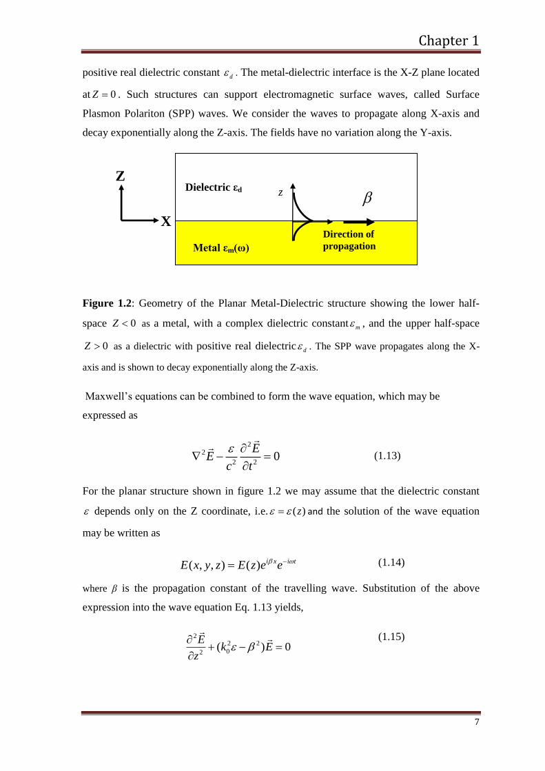
positive real dielectric constant d . The metal-dielectric interface is the X-Z plane located
at 0Z . Such structures can support electromagnetic surface waves, called Surface
Plasmon Polariton (SPP) waves. We consider the waves to propagate along X-axis and
decay exponentially along the Z-axis. The fields have no variation along the Y-axis.
Figure 1.2: Geometry of the Planar Metal-Dielectric structure showing the lower half-
space 0Z as a metal, with a complex dielectric constant m , and the upper half-space
0Z as a dielectric with positive real dielectric d . The SPP wave propagates along the X-
axis and is shown to decay exponentially along the Z-axis.
Maxwell’s equations can be combined to form the wave equation, which may be
expressed as
For the planar structure shown in figure 1.2 we may assume that the dielectric constant
depends only on the Z coordinate, i.e. ( )z and the solution of the wave equation
may be written as
where β is the propagation constant of the travelling wave. Substitution of the above
expression into the wave equation Eq. 1.13 yields,
22
2 20
EE
c t
(1.13)
( , , ) ( ) i x i tE x y z E z e e (1.14)
22 2
02( ) 0
Ek E
z
(1.15)
Z
X x
z
Metal εm(ω)
Dielectric εd
Direction of
propagation

Chapter 1
8
To analyse the modes supported by the planar structure in detail we substitute Eq. 1.14
into Eq. 1.11 and Eq. 1.12 and obtain the following coupled equations
These coupled equations may be solved to obtain two linearly independent solutions
termed as TM-mode and TE-mode having the following field configurations:
Transverse Magnetic (TM) mode (P mode) - No magnetic field component in the
direction of propagation and the only nonzero components are Ex, Hy, and Ez
Transverse Electric (TE) mode (S mode) - No electric field component in the
direction of propagation and the only nonzero components are Hx, Ey and Hz
For the TM-polarized SPP propagating at the metal-dielectric interface (Figure. 1.2) the
system of governing equations and the wave equation are,
The solutions for the above equations in the dielectric region 0Z may be written as
0
y
x
Ei H
z
(1.16)
0x
z y
Ei E i H
z
(1.17)
0y zi E i H (1.18)
0
y
x
Hi E
z
(1.19)
0x
z y
Hi H i E
z
(1.20)
0y zi H i E (1.21)
0
1 y
x
HE i
z
(1.22)
0
z yE H
(1.23)
2
2 2
02( ) 0
y
y
Hk H
z
(1.24)
( ) dk zi x
y dH z A e e
(1.25)
0
1( ) dk zi x
x d d
d
E z iA k e e
(1.26)

Chapter 1
9
In the metallic region 0Z , the solutions become
These solutions must satisfy the boundary conditions that Ex and Hy be continuous across
the interface Z = 0. Application of the boundary conditions yields the following relations:
Figure 1.3: Dispersion relation for SPPs propagating along the metal-air interface.
For the TM mode to propagate as a surface wave it must be ensured that mRe [ ] 0k
since practically for any dielectric Re 0dk . Thus, the surface plasmon waves exist only
at interfaces between materials with opposite signs for the real part of their dielectric
0
( ) dk zi x
z d
d
E z A e e
(1.27)
( ) mk zi x
y mH z A e e (1.28)
0( ) mk zi xmx m
m
E z iA e ek
(1.29)
0
( ) mk zi x
z m
m
E z A e e
(1.30)
m dA A (1.31)
d d
m m
k
k
(1.32)

Chapter 1
10
permittivity, i.e. a conductor-insulator interface. Further, the expression for Hy has to
satisfy Eq.1.24, the wave equation, yielding the dispersion relations:
Combining Eq. 1.32 to 1.34, the dispersion relation for SPPs propagating along the
interface between the metal and dielectric is given by,
The dispersion relation for the SPP waves is shown in figure. 1.3. The SPP curve always
lies to the right of the light-line, and hence the SPP has a larger wave vector than that for
light propagating in an infinite dielectric medium. Thus, Surface plasmons are transverse
magnetic (TM) in character and the generation of surface charge requires an electric field
normal to the surface. This character also leads to the field component perpendicular to
the surface being enhanced near the surface. The field pattern transverse to the interface is
seen to be evanescent and, hence, prevents wave power from propagating away from the
interface. (Stefan A Maier. 2006).
If we consider the possibility of TE surface wave, using the respective expressions for
TE field components from the coupled equation, gives the following boundary condition
that Hx and Ey be continuous across the interface Z = 0.
Since confinement to the surface requires Re [km] < 0 and Re [kd] > 0, this condition is
only fulfilled if Am = 0, so that also Ad = Am = 0. Thus, no surface modes exist for TE
polarization. Surface plasmon polaritons only exist for TM polarization.
1.1.4. SPP propagation in a 3-layer metal-insulator-metal (MIM) device
The simplest geometry to analyse propagation of SPPs is metal insulator (MI) structure.
In order to analysis SPP in a waveguide configuration, we have to consider a multilayer
structure consisting of alternating conducting and insulator layers. Each single interface
2 2 2
0m mk k (1.33)
2 2 2
0d dk k (1.34)
0m d
m d
k
(1.35)
0m m dA k k
m dA A
(1.36)
Chapter 1
11
can support bound SPPs. If the separation between the interfaces is comparable to or
smaller than the decay length of the propagating mode the structure supports coupled
modes.
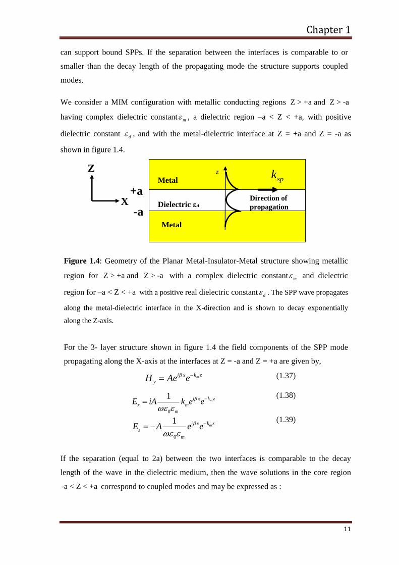
We consider a MIM configuration with metallic conducting regions Z > +a and Z > -a
having complex dielectric constant m , a dielectric region –a < Z < +a, with positive
dielectric constant d , and with the metal-dielectric interface at Z = +a and Z = -a as
shown in figure 1.4.
Figure 1.4: Geometry of the Planar Metal-Insulator-Metal structure showing metallic
region for Z > +a and Z > -a with a complex dielectric constant m and dielectric
region for –a < Z < +a with a positive real dielectric constant d . The SPP wave propagates
along the metal-dielectric interface in the X-direction and is shown to decay exponentially
along the Z-axis.
For the 3- layer structure shown in figure 1.4 the field components of the SPP mode
propagating along the X-axis at the interfaces at Z = -a and Z = +a are given by,
If the separation (equal to 2a) between the two interfaces is comparable to the decay
length of the wave in the dielectric medium, then the wave solutions in the core region
-a < Z < +a correspond to coupled modes and may be expressed as :
mk zi x
yH Ae e (1.37)
0
1mk zi x
x m
m
E iA k e e
(1.38)
0
1mk zi x
z
m
E A e e
(1.39)
Z
X x
zspk
Metal
εm(ω)
Metal
εm(ω)
Dielectric εd Direction of
propagation
+a
-a

Chapter 1
12
The requirement of continuity of Hy and Ex across the interfaces leads to
Solving the above system of linear coupled equations leads to the dispersion relation or
the characteristic equation for the propagating TM SPP mode in the MIM structure.
where, m is the frequency dependent permittivity of metal and d is the dielectric
permittivity of the insulator. And the + and signs indicate the symmetric and anti-
symmetric solutions for the propagating TM SPP modes.
Figure 1.5: (a) Ex and Hy Field component of symmetric TM SPP mode at the MIM
waveguide. (b) Dispersion relation of the coupled SPP mode of the MIM waveguide for
different waveguide width (G).
d dk z k zi x i x
yH Ce e De e
(1.40)
0 0
1 1d dk z k zi x i x
x d d
d d
E iC k e e iD k e e
(1.41)
0 0
d dk z k zi x i x
z
d d
E C e e D e e
(1.42)
m d dk a k a k aAe Ce De
(1.43)
m d dk a k a k a
m d d
m d d
A C Dk e k e k e
(1.44)
tanh m dd
d m
kk G
k
(1.45)
(a) (b) (a)

Chapter 1
13
Figure 1.5 (a & b) shows the TM SPP field profiles in the MIM waveguide structure
and the dispersion relation for the mode. When SPPs are excites at a metal dielectric
interface, electrons in the metal creates a surface polarization that gives rise to a
localized electric field. Metals are lossy and the SPP modes at the interface can
propagate over several microns. From the dispersion relation, it is seen that the
propagation constant does not go to infinity as the SPP frequency is reached, but folds
back and eventually crosses the light line, as is true for SPPs propagating at single
interfaces. Large propagation constants can be achieved for excitation well below the
SPP frequency provided the width of the dielectric layer is in the order of 2 .
Adjusting the thickness of the dielectric region provides access to larger propagation
length and smaller field penetration into the metallic layers.
1.2 THz TIME DOMAIN SPECTROSCOPY
Figure 1.6 shows the THz time domain spectroscopy (THz-TDS) setup used for
our experiments. It consists of a femtosecond (fs) Ti: Sapphire (10 fs pulse-width) laser
with 800nm wavelength and repetition frequency of 76 MHz. The optical pulses are
focused onto the inner edge of the input terminal of a coplanar strip line on a biased semi-
insulating LT: GaAs wafer. Each pulse creates an electron-hole pair and the subsequent
acceleration of these carriers by the bias field, generates a near single-cycle linearly
polarized electromagnetic pulse of THz radiation. In the standard THz TDS setup, the
sample under investigation is placed at the beam waist between the two off-axis parabolic
mirrors, which are in the confocal configuration. The transmitted THz is collected by
another pair of parabolic mirrors and detected by a ZnTe <110> based electro-optic
detection setup.
The transmitting antenna is at the focus of a hyper hemispherical lens, made of high
resistance silicon, which collimates the far field pattern into a Gaussian beam with a 1/e
beam width of 5 mm. The beam waist forms in the focal plane of the parabolic mirror,
which focuses the beam to a second beam with diameter (200µm) proportional to the
wavelength. The combination of the parabolic mirror, silicon lens and antenna chip
constitutes the THz transmitter, which generates a highly directional, freely propagating
beam of picosecond THz pulses.

Chapter 1
14
Figure 1.6: Standard THz time domain spectroscopy (THz TDS)
The dotted line in figure 1.6 is a box, partially sealed and connected to dry nitrogen tank
creating a low humidity environment inside. This is required as even a small trace of
water in the THz beam path will absorb a large amount of the radiation.
The ultra short pulse in the detection path is incident upon a retro-reflector on an electro-
mechanical delay line called the delay stage. This delay stage enables us to delay the laser
pulse accurately relative to the THz pulse signal from the sample.
Figure 1.7: Typical traces of the THz Time domain spectroscopy. (a) Raw data in the
time domain (b) Corresponding numerical Fourier transform of the time domain signal.
0 5 10 15 20 25 30 35 40 45 50-1.0
-0.5
0.0
0.5
1.0
Sig
na
l (m
V)
Time (ps)
0.5 1.0 1.5 2.0 2.5 3.01E-3
0.01
0.1
1
Am
pli
tud
e (
a.u
.)
Frequency THz
(a) (b)

Chapter 1
15
At the detection end, the THz pulse and the probe pulse propagate in the detection crystal,
a ZnTe crystal of thickness 0.5 mm. The beam then passes through a quarter-wave plate
and Wollaston prism that splits the beam into two plane polarized light beams. These two
beams are focussed onto the two photo-diodes of the differential detector. The difference
in the signal is sent to the lock-in amplifier. This measured difference in the intensity of
the two beams is directly related to the terahertz electric field strength. Thus the terahertz
field can be plotted against time. An example of this is shown in figure 1.7a. The Fourier
Transform of the temporal THz pulse is computed to obtain the frequency spectrum of the
THz electric field (Figure 1.7b).
1.3 LITERATURE REVIEW
Earliest work related to plasmonics dates back about 100 years when Sommerfeld
(1899) and later Zenneck (1907) presented theoretical analysis of surface waves on metal
surfaces. Equally important was the seminal work of Paul Drude (1900) on conductivity
of metals, which in turn can be related to the refractive index of metals. The next
important development was the classic work of Ritchie (Ritchie 1957) in which he
demonstrated the excitation of surface plasmon waves in experiments on electron
diffraction by thin metal foils. A little later in 1968, Kretschmann and Raether showed
that surface plasmon waves can be excited optically on metal surface by employing the
prism-coupling technique (Sambles et al. 1991). Thus the phenomenon of Surface
Plasmon Polariton (SPP) was established. These developments led to research on several
devices, all working at optical wavelengths. Much of the past works have been well
described in the monograph on “Surface Plasmons” by Heinz Raether (1988). Further,
towards the end of 20th century, interest in plasmonic devices operating at Terahertz
frequencies picked up. The last 15 years have seen a rapid growth of research in this new
domain of Plasmonics. In what follows, we present a brief summary of the literature on
plasmonic devices over the past two decades.
1.3.1 Surface Plasmons
Waveguides are used for a controlled transport of electromagnetic radiation with
minimum loss and dispersion (Keiser 1991). Thus waveguides, especially thin film stripe
or channel types, are an essential part of any signal processing or imaging or sensing

Chapter 1
16
system/chip. Initial studies focused on thin film waveguides having either Insulator-
Metal-Insulator (IMI) or Metal-Insulator-Metal (M-I-M) configuration designed for
optical wavelengths (Burton and Cassidy 1990, Prade et al. 1991, Berini et al. 1996,
Tournois and Laude 1997, Berini et al. 2000). Experimental confirmation of the existence
of surface plasmon waves was reported very soon (Marti et al. 1993, Webber et al. 2001)
and the young field of plasmonics rapidly expanded in new directions in the late 1990s
and early 2000s.
At that time it was demonstrated that plasmon propagation in,
Metallic nanowires can guide light well below the seemingly unsurpassable
diffraction limit (Takahara et al. 1997).
Metal film with nanoscale holes show extraordinarily high optical transmission
(Ebbesen 1998).
Simple thin film of metal can serve as an optical lens (Pendry 2000).
Diffraction of waves limits the size of the aperture for light transmission. However,
metallic thin films, with an array of apertures, yielded unusually high light transmission at
wavelengths as large as ten times the diameter of the aperture (Pendry et al. 2001,
Ebbesen et al. 2002). This phenomenon was related to excitation of surface plasmon (SP)
waves at the metal interfaces, leading to extraordinarily high light transmission.
Propagation of surface plasmon waves on a flat metal surface gets significantly attenuated
owing to absorption in the metal. This attenuation depends on the dielectric properties of
the metal at the frequency of the SP waves (Barnes et al. 2003). Studies on thin film stripe
of gold on a glass substrate (Lamprecht et al 2001) revealed bound SP mode propagation
at the metal dielectric interface. Devices having MIM geometry, made using thin film of
Au or Cu or Al metal, show higher confinement of SP mode compared to a device in the
IMI geometry (Zia et al. 2004). SP wave propagation in triangular (V) groove on gold
films (Bozhevolnyi et al. 2005) and plasmon slot waveguide (Veronis et al. 2007) at
telecommunication wavelength (1425 – 1620nm) showed low-loss for a waveguide of
width of 600nm and film thickness of 1µm; propagation length of 100µm was achieved.
Further advances on plasmonic MIM waveguide devices focused on waveguides with
stubs (Matsuzaki et al. 2008) and bends (Veronis et al. 2005). Studies on optical
transmission of these devices revealed that they function as narrow band optical filters on
account of interference occurring between the waves travelling in the forward and reverse

Chapter 1
17
directions. This aspect was explored analytically by modeling the devices as equivalent
RLC circuits derived from Transmission Line theory (Pannipitiya et at. 2010).
Investigations on the dispersion relations and wave attenuation in two-dimensional
Ag/SiO2/Ag structures for waveguide thickness ranging from 12 nm to 250 nm ( Dionne
et al. 2005, Dionne et al. 2006) led to better understanding of MIM type devices (Stefan
Maier 2006). Characteristics of forward and the backward propagating guided SP waves
was studied taking wave energy losses into account (Bozhevolnyi et al. 2010). MIM
waveguide device made using gold film of thickness 60nm, (Yang et al. 2014) was
observed to show highly efficient SP wave excitation and propagation. Very recently,
plasmonic devices have been made using Graphene (Stefan Maier 2012). Such devices
show strong mode confinement, wavelength tunability and long lived collective plasma
oscillations (Grigorenko et al. 2012). Graphene plasmonic waveguide, with a monolayer
of graphene on dielectric substrates has the potential to provide smaller loss and longer
propagation lengths (Vakil et al. 2011, Zhu et al. 2013, Zheng et al. 2015).
Compared to the studies on plasmonic devices at visible light frequencies, fewer works
have been reported on devices operating in the terahertz frequency regime (Masayoshi
2007, Isaac et al. 2008, Gallant et al. 2007, Vinconzo e al. 2010). This dissertation
focuses on the properties of SP wave propagation in THz waveguide device and its
application as chemical sensors.
1.3.2 Terahertz waveguide devices
THz pulses of subpicosecond duration were first generated using optoelectronic methods
(Auston et al. 1980) using coplanar waveguide devices. However, pulse distortion due to
frequency dependent loss and dispersion (Cooper 1985) was a problem. This was
overcome by the use of photoconductive dipole antenna (PCA) for generating and
detecting THz pulses, avoiding the use of waveguides (Auston 1984). Subsequently,
techniques were developed to improve the coupling efficiency of the generated and
detected pulse (Fattinger et al. 1988, McGowan et al. 1999). New designs of PCA also
emerged with increased power and operation bandwidth. These new sources were used
for free space propagation with very low loss.
In the early 1990’s biomedical applications of THz radiation were limited by large
diffraction limited focal spot size, requiring the use of large sized bio-samples. This

Chapter 1
18
problem may be overcome by using waveguide devices. However, guided wave devices
suffer from excessive power loss and pulse distortion. Towards the end of 1990’s, ways to
overcome these hurdles were proposed by Daniel Grischkowsky and others (McGowan et
al. 1999, Grischkowsky 2000). The new waveguide devices were robust and were simple
to integrate into the already available THz systems. More importantly, they allow stronger
interaction between the THz radiations with the sample loaded into the waveguide.
THz waveguides were fabricated by sawing a 270µm wide slit through a 40 mm wide and
300 µm thick silicon slabs with subsequent metallization of all faces. Low-loss
propagation with negligible group velocity dispersion was observed in the 0.1–1 THz
frequency range (Wächter et al. 2007). Sub-wavelength array of rectangular slots in
semiconductors (Silicon and Indium Antimonide) exhibited stronger electric field at the
edges, compared to metal slots, on propagation of THz radiation through periodic
structures (Gelmont et al. 2008). It was suggested that such field enhancement is due to
excitation of surface plasmons. This phenomenon may be exploited in novel bio-sensors.
The potential for sensor applications has driven intensive investigations on different
waveguide structures using a variety of materials, both metals and semiconductors. Some
of the significant contributions on the characteristics of THz plasmonic devices are:
THz SP localization within a nanoporous silicon slab (Lo et al. 2010).
Periodic rectangular apertures on metal foil as a complex planar plasmonic THz
waveguide device (Zhu et al. 2011).
Subwavelength confinement of THz SP in tapered parallel plate waveguide
(PPWG). (Zhan et al. 2011).
Micromachining rectangular stubs on PPWG as resonant cavity to observe
electromagnetically induced transparency (EIT) (Mendis et al. 2009, Chen et al.
2013, Kimberly et al. 2014, Steven 2014).
In any plasmonic device, excitation of surface plasmon waves is a prime requirement.
While metals, like gold and silver, are suitable for optical radiations, semiconductors are
appropriate for devices designed to work at THz frequencies since they have a much
lower permittivity than metals at THz frequencies. Further, their much lower free carrier
concentration leads to plasma waves in the THz regime. For waveguide device made of
semiconductors, their permittivity allows for a strong coupling of the THz field to free
charges at the semiconductor-dielectric interface resulting in a propagating surface wave.
Further, the carrier concentration in semiconductors may be modulated thermally or

Chapter 1
19
optically, besides appropriate doping, to match a specific THz frequency, making them
promising candidates for tuneable plasmonic devices in the THz domain.
THz radiation may be used to probe the vibration and rotational modes of biomolecules,
like proteins, DNA, RNA, leading to a variety of promising bio and chemical sensors.
Such studies were carried out by the technique of THz Time Domain Spectroscopy (TDS)
since early 2000. Initially the samples were taken in cuvettes and, hence, required large
quantities of the sample. Later several groups worked on THz Plasmonic devices and
demonstrated detection with high sensitivity. Some of the significant contributions on
such plasmonic sensors are listed below:
PPWG devices for high resolution THz spectroscopy to study a specific vibration
mode for several protein molecules (Laman et al. 2008)
THz antenna (Berrier et al. 2012) was used to detect bacterial layers with high
sensitivity. These THz sensors can sense ultra-thin (a few nanometer thick)
molecular layers (John et al. 2008) and a few femto-moles of DNA molecules.
THz dielectric pipe waveguide was used for detecting vapours of hydrochloric
acid, acetone, ammonia and water with a minimum detectable molecular density
as low as 1.6 nano-mole/mm3 (You et al. 2012).
A THz metamaterial device, consisting of symmetric split ring resonators, was
exploited as ultrasensitive refractive index sensor, possessing a sensitivity of 36.7
GHz/RIU and 23.9 GHz/RIU when Fano and Quadrupole resonances,
respectively, were excited (Singh et al. 2014).
1.4. SCOPE AND OBJECTIVES OF THE THESIS WORK
Terahertz science is acquiring multi-disciplinary dimensions. It has drawn ideas
from photonics, electronics, material science and nanotechnology and has applications in
signal processing, spectroscopic analysis of materials, detection of explosive and
hazardous materials and sensors. Plasmonic sensors at THz frequencies are especially
suited for sensing bio-molecules.
This thesis focuses on developing a novel THz plasmonics sensor consisting of a
waveguide, with stubs along the waveguide. Such devices exploit the phenomenon of
surface plasmon waves and function as resonant devices. The resonant characteristics of
Chapter 1
20
the device lead to strong localization of electric fields in the stubs and this facilitates a
strong interaction of the THz wave with any material present in the stub. Waveguide
devices were fabricated using intrinsic Indium Antimonide (InSb) and their propagation
characteristics at THz frequency were experimentally investigated. The sensing property
of the device was also studied. The main research objectives of the Thesis were:
1. To model the dielectric properties of Indium Antimonide at THz frequencies.
2. To study the transmission characteristics of InSb plasmonic devices using
simulation tools such as COMSOL Multiphysics and Ansoft HFSS.
3. To model the plasmonic device as an equivalent RLC circuit.
4. To fabricate the designed InSb plasmonic device by laser micromachining.
5. To investigate the transmission characteristics of the waveguide without stub
(straight waveguide) and waveguide with two stubs using THz TDS technique.
6. To investigate the sensing capability of the device by loading the protein Bovine
Serum Albumin (BSA) and polystyrene dissolved in toluene into one of the stubs
of the device and measuring the transmission coefficient using THz TDS
technique.
The work presented in the thesis is divided into six chapters. A brief summary of the
contents of each chapter is given below.
Chapter 1 contains a general introduction to Plasmonics, theoretical aspects of surface
plasmon propagation at metal – dielectric and metal- dielectric-metal interfaces. Next, the
details of THz TDS technique are discussed. Literature survey of the research work on
THz waveguide devices and their applications as chemical and biosensor are presented.
The scope and objectives of the present work are mentioned at the end of this chapter.
Chapter 2 presents the relevance of semiconductors for THz devices, modelling of the
frequency dependent dielectric permittivity of InSb using Drude free electron model
along with simulation and numerical investigation of THz InSb plasmonic waveguide
using effective index method (EIM). Effective index approach is applied for modelling
surface plasmon polaritions (SPPs) propagation in InSb planar waveguide. The effective
index of the propagating mode along with the corresponding propagation lengths are
calculated for different configurations at THz wavelengths while varying the trench

Chapter 1
21
depth. The confinement of SPPs in the trench along with the variations in the propagation
length for different trench dimensions is discussed.
Chapter 3 describes the simulation studies using COMSOL Multiphysics and Ansoft
HFSS on THz InSb waveguide with stubs along the waveguide acting as resonant cavity
leading to a narrow band filter. The transmission characteristics and the resonance
features of the waveguide with single and two stubs have been discussed for various
device dimensions like waveguide width and stub length. An attempt has been made to
establish an analogy between InSb waveguide and microwave transmission line by
modelling the device as an equivalent RLC circuit. The transmission spectra of the
simulated and analytically calculated InSb waveguide with stub are compared and
discussed.
Chapter 4 reports the experimental investigation of THz InSb waveguide device
including fabrication and characterization using THz TDS. The detailed steps involved in
the preparation of InSb pellets, the creation of trench by laser ablation to form waveguide
and stubs on the upper face of the pellet are presented in the first section. THz TDS on the
fabricated InSb waveguide devices showing the dependence of resonance frequency on
waveguide with stub are discussed. Comparison of the simulated and experimental
transmission spectra of the waveguide with stub is made and the plasmon propagation,
together with narrow band filtering characteristics of the waveguide, is also discussed.
Above the cut off frequency the device shows transmission maxima and minima as a
function of frequency. This can be attributed to the interference between the forward
propagating wave and the wave reflected from the stub.
Chapter 5 focuses on exploiting the resonance characteristics of the THz InSb waveguide
device as a novel sensor. A well known protein molecule, Bovine serum albumin (BSA)
and polymer sample, polystyrene dissolved in toluene, are used for evaluating the sensing
capability of the waveguide. Loading one of the stubs in the device with one of the
sample materials, changes the refractive index of the medium inside the stub. The change
in the transmission and absorption coefficient of the device by varying the concentration
of the medium is studied and presented. Substantial improvement in the sensitivity of the
device for only a few micro litre quantity of the sample is observed. The potential
application of InSb waveguide as a promising sensor is discussed.

Chapter 1
22
Chapter 6 summarizes the main results and conclusions of this research work.
Suggestions for future research on this topic are mentioned. The chapter ends with
references, a list of publications and the author’s bio-data.

Chapter 2
23
CHAPTER 2
MODELLING OF InSb PLASMONIC THz WAVEGUIDE
Abstract
In this chapter we present the results of modelling and simulation of the propagation
characteristics of electromagnetic waves, at THz frequencies, in a channel waveguide
made using InSb. We focus on SPP propagation along the semiconductor-insulator (SI)
interface. The Effective Index method has been employed to study the SP propagation in
the channel waveguide of sub-wavelength width. We have investigated the strength of the
wave electric field close to the interface and also the propagation losses at THz
frequencies.
2.1. INTRODUCTION
THz plasmonic devices exploit the coupling of THz electromagnetic waves with the
collective oscillation of the free electrons in the medium. This coupling of the wave to the
surface is maximum for frequencies close to the plasma frequency of the metal or
semiconductor. The plasma frequency of metals lies, typically, in the visible or ultraviolet
part of the electromagnetic spectrum. At THz frequencies the EM wave is no longer a
surface wave for metals as the electromagnetic fields get highly delocalized.
Semiconductors have a much lower plasma frequency than metals, typically in the
terahertz frequency range, allowing strong localization of THz SPPs to the
semiconductor-dielectric interface. Another crucial difference between metals and
semiconductors is that semiconductors are much more versatile materials since their
plasma frequency may be tuned by appropriate doping. Switching of the SPP-assisted
resonant THz transmission through hole arrays has been demonstrated using electrical
(Chen et al. 2008), optical (Hendry et al. 2008) and thermal (Rivas et al. 2004)
techniques. Also efficient real-time control and manipulation of THz SPPs using active
metamaterial resonant semiconductor devices enables improved modulation of THz

Chapter 2
24
transmission over existing devices (Chen et al. 2006). Consequently semiconductors are
promising candidates for active Plasmonic devices at THz frequencies.
2.2 IMPORTANCE OF InSb IN THE THz FREQUENCY REGIME
Among the III-V binary semiconductors, Indium Antimonide (InSb) has attracted
considerable attention over the last several years. Many of its interesting properties are
directly associated with its very low effective electron mass and high electron mobility. It
has the smallest band gap among other III-V binaries, measuring 0.17eV at 300K that
corresponds to IR wavelength and the material is therefore useful as an infrared detector
and filter (Koichiro et al. 2013).
In order to fully describe the properties of InSb, relevant to plasmonic devices, the
expression for frequency dependent permittivity is required for calculating the attenuation
and propagation of SPPs. Time resolved studies of carrier dynamics (electrons and holes)
in semiconductors (Exter et al. 1990) have shown that the permittivity of semiconductors
at THz frequencies is well described by the Drude model for free electrons.
Figure 2.1: Real and Imaginary part of the complex permittivity of InSb calculated using
Drude free electron model.
The expression for the dielectric permittivity is given by
2
2( )
p
i
(2.1)

Chapter 2
25
where, the high frequency permittivity = 15.75, ~ 1.25 THz is the carrier collision
frequency for InSb and the plasma frequency is given by
22
0 *p
Ne
m
which depends on
the electron number density N and its effective mass m*; for InSb m* = 0.014 me , where
me is the free electron mass.
The carrier density depends significantly on temperature, doping level and on absorption
of visible light photons. The intrinsic carrier density N of InSb (Jin et al. 2013) is given
by 14 1.5 35.76 10 exp( 0.129 ) BN X T k T cm . At 300K the ε(ω) of InSb at 0.3THz is -
91.54+15.67i which is similar to that of metals at optical frequencies.
From the expression of the plasma frequency, it follows that the permittivity depends on
the carrier concentration and carrier mobility. The plasma frequency for InSb is in the
THz range. Therefore the value of permittivity of InSb at THz frequencies is close to that
of metals in the visible and near infrared frequencies, i.e. the permittivity has a real
negative part with a small absolute value and a small imaginary component related to
energy absorption. In contrast, the permittivity of gold at THz frequencies has a very
large negative real value and a large imaginary component. These values, several orders
of magnitude larger than those of InSb are due to the higher plasma frequency of gold
compared to InSb. The difference in plasma frequency between InSb and gold is mainly
determined by the much higher free carrier density of metal. Hence, just as metal surfaces
support SPPs at visible frequencies it is expected that SPPs should also propagate on the
surface of InSb at THz frequencies.
2.3. SURFACE PLASMON MODES IN InSb WAVEGUIDE
Propagation properties of THz InSb waveguide structures were simulated and analyzed
using COMSOL Multiphysics and Ansoft HFSS softwares. The frequency dependent
permittivity of InSb at THz frequencies was calculated using Drude model. The
waveguides were modelled as a channel waveguide surrounded by air with spatial grid
size chosen to ensure convergence of the numerical calculations. Perfectly matched layer

Chapter 2
26
Figure 2.2 (a) Schematic of InSb channel waveguide of width G and length A.
Transverse Hy component of the TM SPP propagating along the SIS interface for (b) G
= 100µm, (c) G = 500µm, (d) G = 1000µm at different length A of the InSb channel
waveguide.
(a)
(b)
(c) (d)
absorbing boundary conditions were applied at all the boundaries. TM polarized THz
wave was incident on the input port. SPP propagation along the waveguide and the
dependence of the transmission characteristics on the waveguide dimensions were
analyzed.
Figure.2.2 shows that the guided mode pattern depends on the width of the waveguide.
Theoretical analysis indicates that the cut-off frequency of the waveguide with
rectangular cross section depends solely on the depth (D) of the waveguide (Zhu et al.
2011); cut-off frequency fc = c/2D. The propagation characteristics of InSb channel
waveguide of depth (D) = 1800µm were obtained by simulation for varying waveguide
width G. Figure 2.2b shows the Hy component of the SPP mode for G = 100µm, 500µm
and 1000µm with the decay length of ~50 µm, ~120 µm, ~150 µm respectively . The
mode field associated with the propagating mode has a large transverse (Hy) component.
As the width of the waveguide decreases, the intensity of the Hy component leaking into
Chapter 2
27
the semiconductor waveguide increases and the propagation length of the mode along the
waveguide decreases. Such waveguide devices exhibit strong attenuation of the wave.
Semiconductors are generally lossy and, hence, the SP modes of a semiconductor-
dielectric structure can propagate over several microns. However, in our devices made of
InSb a relatively small portion of the wave energy is carried in the dissipative InSb layer
and hence the mode can propagate over distances of the order of a few millimetres. This
aspect is suitable for THz integrated circuits and interconnects and has inspired a new
class of plasmon channel waveguides in the THz domain. (Jin et al. 2013)
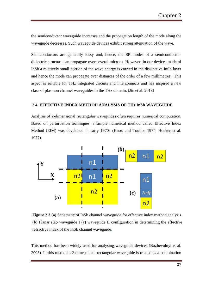
2.4. EFFECTIVE INDEX METHOD ANALYSIS OF THz InSb WAVEGUIDE
Analysis of 2-dimensional rectangular waveguides often requires numerical computation.
Based on perturbation techniques, a simple numerical method called Effective Index
Method (EIM) was developed in early 1970s (Knox and Toulios 1974, Hocker et al.
1977).
This method has been widely used for analysing waveguide devices (Bozhevolnyi et al.
2005). In this method a 2-dimensional rectangular waveguide is treated as a combination
Figure 2.3 (a) Schematic of InSb channel waveguide for effective index method analysis.
(b) Planar slab waveguide I (c) waveguide II configuration in determining the effective
refractive index of the InSb channel waveguide.
(a)
(b)
(c)
X
Y

Chapter 2
28
of two slab waveguides (labelled here as waveguide I and II) oriented perpendicular to
each other. Essentially the solutions for a 2-dimensional waveguide problem are obtained
in terms of solutions for two 1-dimensional problems.
We consider a channel waveguide as shown in figure 2.3. To apply the effective index
method, waveguide I (Figure.2.3b) is treated as a slab waveguide extending in the y-z
plane. Modal analysis of this slab waveguide yields the value of propagation constant β of
the mode of our interest and using this, the effective index, neff , is calculated using
0
effnk
(2.2)
where k0 is the wave number in vacuum. This effective index is now assumed to be the
refractive index for the core region of waveguide-II, which is also a slab waveguide
extending in the x-z plane (Figure 2.3 (c)). It may be noted that with this prescription,
waveguide-II becomes an asymmetric waveguide. Modal analysis of waveguide-II yields
the propagation constant (β) for the desired mode, which should be a TM-mode in order
to represent SPP mode for the channel waveguide. It is easy to see that only a TE-mode of
waveguide-I leads to the TM-mode for waveguide-II.
We have carried out the modal analysis for TE-mode for waveguide-I using the following
characteristic equation to determine β for the symmetric mode,
2 2
2tanh d s
d
d s
kk G
k
(2.3)
where 2 2 2
0s sk and 2 2 2
0d dk k , ko is the free space wave number of the
electromagnetic wave. The solution of the above equation yields β values for the guided
mode and using this value neff can be calculated from Eq.2.2.
Waveguide-II as shown in Figure.2.3(c) is an asymmetric slab waveguide. For
waveguide-II the mode being considered assumes TM-mode polarisation due to its
different orientation with respect to waveguide-I. Hence, we have computed the
propagation constant β’ for TM-mode for waveguide-II using the following characteristic
equation appropriate for TM modes in asymmetric waveguide

Chapter 2
29
where 2 2 2
0s sk , 2 2 2
0c dk , 2 2 2
0f fk k , 2
f effN , 2
1d n , 2
2s n , ko is
the free space wave number of the electromagnetic wave. In the calculations we have set
εd = 1.0 for the dielectric layer and for the dielectric permittivity of InSb at 0.3THz we
have set εs = (91.54 + 15.67i). The propagation constant β, thus determined, is taken as the
actual value for the SPP mode of the channel waveguide. We have computed β for
varying waveguide width (G) and also waveguide depth (D). The results of the
computations are displayed as graphs shown in Fig. 2.4 and 2.5.
(2.4)
2 2
2 2
2 1
4
2
2 2
1 2
tanh
eff eff
f s c
f
eff
f c s
N Nk
n nk G
Nk
n n
Figure 2.4 The SPP mode (a) Effective index and its (b) Propagation length as a
function of the width G of the InSb waveguide at THz frequencies.
(a) (b)
Figure 2.5 (a) Mode effective index and (b) propagation length as a function of the
depth (D) of the InSb waveguide at 0.1 THz. Parameter ranges correspond to the
single-mode waveguiding regime. The inserts show the cross sectional geometry of the
InSb waveguide.
(a)
(b)
Chapter 2
30
Investigations on the waveguiding properties, i.e., mode effective index, propagation
length, have been performed for wavelengths in the THz range. In regard to the mode
confinement it is advantageous to keep the depth of the waveguide (D) as large as
possible, as it decides the cut-off frequency of the waveguide. The choice of waveguide
width (G), however, is slightly more complicated and is subject to a trade-off between
mode confinement and propagation length. Although the mode effective index increases
monotonously with increase in waveguide width (G), the mode width has a distinct
minimum. This can be envisaged as a point where the field is squeezed into the
waveguide sub-region and when the width is decreased until a certain point, where the
field no longer can be confined to the depth. It then starts to spread out in the surrounding
semiconductor interfaces, where the decay length is larger, thereby increasing the mode
width. These considerations have led to a determination of the optimum waveguide
parameters G ~ 750 µm and D ~ 1500 µm, which ensures mode propagation with sub-
wavelength lateral confinement. A wavelength analysis of the guiding properties of the
InSb waveguide using EIM has been verified by measurements performed on fabricated
samples with dimensions close to the optimum and is described in the next chapter.
2.5. CONCLUSIONS
In summary, InSb THz waveguide supports SPP propagation along the semiconductor
insulator interfaces and the geometrical parameters were optimized to obtain longer
propagation length. The propagation characteristics of InSb channel waveguide were
obtained by simulation for varying waveguide width (G). Hy component of the SPP mode
for the InSb waveguide of width G = 100µm, 500µm and 1000µm had a decay length of
~50 µm, ~120 µm, ~150 µm respectively. The mode field associated with the propagating
mode has a large transverse (Hy) component. As the width of the waveguide decreases,
the intensity of the Hy component leaking into the semiconductor waveguide increases
and the propagation length of the mode along the waveguide decreases. Effective Index
Method has been applied for modelling the SPP propagation in the rectangular channel
waveguide. Investigation on the waveguiding properties, i.e., mode effective index,
propagation length, has been performed for wavelengths in the THz range. The method
has led to a determination of the optimum waveguide parameters G ~ 750 µm and D ~

Chapter 2
31
1500 µm, which ensures mode propagation with sub-wavelength lateral confinement. A
wavelength analysis of the guiding properties on the InSb waveguide using EIM has been
verified by measurements performed on fabricated samples with dimensions close to the
optimum and is described in the next chapter.

Chapter 3
32
CHAPTER 3
TRANSMISSION CHARACTERISTICS OF THE InSb
PLASMONIC DEVICE
Abstract
This chapter presents simulation studies on SPP propagation and the filtering
properties of InSb waveguide device with (a) single and (b) two pair of stubs which
functions as a cavity resonator at THz frequencies. With the excitation of localized
SPs, the study focuses on the transmission and filtering properties of the waveguide
for different stub length and stub width. These waveguide devices with stubs resonate
at particular frequencies called the resonant frequencies and transmitting all other
frequencies. Simulation studies indicate large electric field enhancement in the stubs
at resonance, which is also supported by analytical calculations using the methods of
microwave transmission line network theory.
3.1. INTRODUCTION
The availability of THz sources and detectors has led to rapid progress in the
development of plasmonic waveguide components such as polarisers, filters and
collimators (Masayoshi 2007). In this chapter, we investigate the transmission
characteristics of InSb waveguide device having single and two pair of stubs at THz
frequencies using COMSOL MULTIPHYSICS and Ansoft HFSS software packages.
The filtering characteristics of the device are studied by simulation. Further, a
Transmission Line model is adopted for the device and its transmission characteristics
are evaluated and compared with the simulation results. The investigations have been
carried out by varying device parameters such as waveguide width, stub length and
stub width for devices with a single stub and two stubs. These studies have been
carried out to investigate the resonance features of the devices and the localization of
the wave electric fields along the device, with particular focus on the stubs. The

Chapter 3
33
strength of the electric fields in the stubs would reveal the potential of the device as a
sensor of different materials.
3.2 InSb THz PLASMONIC WAVEGUIDE WITH STUBS
3.2.1 Device Configuration
The schematic of the THz InSb Plasmonic waveguide device investigated in this
thesis is shown in figure 3.1. It consists of a planar semiconductor-insulator-
semiconductor (SIS) structure (discussed in chapter 2) with stubs along the waveguide
to form a resonant structure. The waveguide section and the stubs are made by
creating a trench in an InSb pellet. COMSOL MULTIPHYSICS and Ansoft HFSS,
finite element method based simulation tools, were employed to theoretically analyze
its transmission characteristics.
Microwave Resonators are, typically, rectangular cavities with walls made using high
conductivity metals. Such structures support standing electromagnetic wave patterns
inside the cavity and are characterised by high Quality Factor. They are capable of
storing large quantities of electromagnetic energy. Our plasmonic devices also
possess the capability to store energy due to the inclusion of the stubs. Since any THz
Figure 3.1.Schematic of the InSb waveguide device with two stubs. Typical device
dimensions: (a) Stub length L =1000µm, stub width W = 750µm, width of the
waveguide G = 750µm, position of the stub x = 6mm, and length of the waveguide A
= 12mm (b) Depth of the waveguide D = 1.5mm, thickness of the pellet T = 2mm.
The parameters G and W are kept equal.
(a)
(b)

Chapter 3
34
source has a rather limited output spectrum, these devices are evaluated within this
spectrum as a band-pass filter. The resonant frequency for the device can be tuned by
varying the device dimensions.
3.2.2 Transmission Characteristics
The THz wave was launched at the input port of the waveguide (Figure. 3.1(a)),
exciting the SPP’s at the semiconductor-air interfaces in the waveguide channel. The
SPP’s propagate along the walls of the waveguide and the stubs. The amplitude of the
signal exiting the output port was measured. The wave propagates through the device
showing frequency dependant transmission minimum and maximum at the output
port. Figure 3.2 shows the variation in transmission coefficient as a function of
frequency for different values of stub length L, width of the waveguide G.
The graphs show sharp dips in the transmission at certain frequencies, known as
resonance frequencies, and high transmission over broad frequency ranges. It is seen
that, in the frequency range of our interest, for device parameters L = 450 µm and G =
1000 µm, transmission minimum occurs at only one frequency. When L or G was
increased, the transmission minima occurred at two or more frequencies. As shown in
figure 3.2(a) for G = 1000 µm and L = 450µm, the transmission minimum occurred at
0.236THz and for L = 750µm, minima occurred at two frequencies 0.218THz and
Figure 3.2 Transmission characteristics of InSb THz Plasmonic waveguide device
with stubs functioning as a cavity resonator. (a) Varying stub length (L) with G =
1000µm (b) Varying the width of the waveguide (G = W) with L = 1000µm.
(a)
(b)

Chapter 3
35
0.276THz. These two minima got slightly shifted to 0.213THz and 0.28THz when L
was further increased to 1000µm. As shown in figure 3.2(b) for L = 1000 µm and G =
450µm, the device showed transmission minimum at 0.219THz. For G = 750µm
minima occurred at 0.238THz and 0.292THz and for G = 1000µm the minima shifted
to 0.213THz and 0.28THz. Thus, it is clear that by choosing the sizes G or L, the
device can be designed to possess a single or multiple resonance frequencies within
the frequency range of the THz source used.
Figure 3.3 shows the electric field pattern of the SPP mode propagating in the device
along with the corresponding electron density pattern representing the plasma wave
inside the semiconductor. Due to partial reflection of the waves at the stub junction
stationary waves exist together with travelling waves in the device. At the resonance
frequency the stationary wave formation is maximum leading to overall transmission
minima for the device.
Figure 3.3 Simulated THz electric field and corresponding charge density distribution
in the InSb Plasmonic waveguide device with dimensions G = 750 µm, L = 1000 µm.
(a & c) Indicate maximum transmission at 0.3 THz; (b & d) Indicate minimum
transmission at 0.238 THz. (a) and (b) show electric field pattern at 0.3THz and
0.238THz, respectively; (c) and (d) show the charge density profile at 0.3THz and
0.238 THz, respectively.
(b) (a)
(c) (d)

Chapter 3
36
Figure 3.3(a) shows the electric field profile of the propagating wave at 0.3THz and
figure 3.3 (b) shows the pattern at the resonant frequency 0.238 THz for G = 750μm
and L = 1000μm. Clearly, the resonant dip at 0.238 THz can be correlated to the
localization of the electric field of the propagating EM wave in the two stubs leading
to strong reflection of the wave back towards the input port. This is also confirmed by
the plots of the charge density distribution at 0.3THz and 0.238 THz as shown in
figure 3.3 (c) and figure 3.3 (d), respectively. At frequencies away from the resonant
frequency, the electromagnetic wave experiences very small impedance mismatch at
the waveguide-stub joints and, hence, propagates freely towards the exit of the
waveguide indicating high transmission. Further, it is also seen that the magnitude of
electric field in the stubs is very small at off-resonant frequencies.
3.3 TRANSMISSION LINE MODEL FOR THE DEVICE
The transmission characteristics of the InSb waveguide with single and more number
of stubs can be analysed by using the transmission line theory employed normally at
microwave frequencies.
The transmission line equivalent circuit for our device is shown in figure 3.4. The
infinite transmission line has a characteristics impedance of ZSIS corresponding to the
waveguide. The stub along the waveguide is modelled as a finite transmission line
x = 0
ZStub INPUT OUTPUT
x = x x = A
ZSIS
ZL
Figure 3.4 (a) Schematics of SIS InSb waveguide device with single stub.
(b) Equivalent Transmission line representation with ZSIS the characteristic
impedance of the SIS waveguide, Zstub the effective stub impedance, ZL the load
impedance. (Pannipitiya et al. 2010)
(a) (b)
Chapter 3
37
with characteristics impedance ZC terminated by a load impedance ZL. The load
impedance ZL is responsible for the reflection and interference of the SPP modes
entering and exiting the cavity.
The above mentioned impedances are expressed in terms of device parameters G, W,
L, propagation constant (β) and permittivity of the insulator region (εair) and
semiconductor (εInSb). The voltage and current wave in a transmission line correspond
to the electric and magnetic fields of the SPP mode. Thus the characteristic impedance
of the waveguide and the stub has the form (Veronis et al. 2005)
0
y
SIS
z Air
E G GZ
H
(3.1)
0
y
C
z Air
E W WZ
H
(3.2)
where ε0 is the permittivity of vacuum. It is considered that the energy of the SPP
mode is mainly confined in the dielectric region and the transverse electromagnetic
field is uniformly distributed along the y axis.
The propagation constant β is calculated from the dispersion relation of SPP modes.
1
1 2 1
1 2
tanh2
ik h k
k
, where ± corresponds to the symmetric and antisymmetric
mode Ex(y) = ±Ex (-y), 2 2
i ik k (i=1,2 ) and εi corresponds to the relative
permittivity of the ith medium.
The load impedance ZL, accounts for the SPP mode reflection from the ends of the
stub. We assume that the SPP undergoes a normal reflection from the stub end and
calculate the reflection coefficient using the equation (Pozar 1998)
InSb AirL S
L S InSb Air
Z Z
Z Z
(3.3)
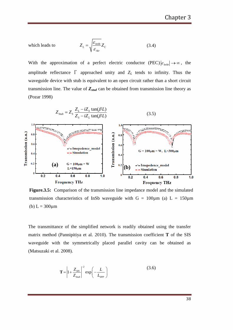
Chapter 3
38
Figure.3.5: Comparison of the transmission line impedance model and the simulated
transmission characteristics of InSb waveguide with G = 100µm (a) L = 150µm
(b) L = 300µm
(a) (b)
which leads to InSbL C
Air
Z Z
(3.4)
With the approximation of a perfect electric conductor (PEC)InSb , the
amplitude reflectance approached unity and ZL tends to infinity. Thus the
waveguide device with stub is equivalent to an open circuit rather than a short circuit
transmission line. The value of Zstud can be obtained from transmission line theory as
(Pozar 1998)
tan( )
tan( )
L SStub S
S L
Z iZ LZ Z
Z iZ L
(3.5)
The transmittance of the simplified network is readily obtained using the transfer
matrix method (Pannipitiya et al. 2010). The transmission coefficient T of the SIS
waveguide with the symmetrically placed parallel cavity can be obtained as
(Matsuzaki et al. 2008).
2
1 expSIS
Stub SPP
Z L
Z L
T
(3.6)

Chapter 3
39
To illustrate the above transmission line model, for InSb waveguide we consider the
parameters G = 100μm = W for L =150μm (figure 3.5(a)) and 300μm (figure 3.5(b)).
Figure 3.5 shows the comparison between the transmission line model (Impedance
model) and the simulation. Eq 3.1 – 3.6 were used to calculate the transmission of the
InSb waveguide with symmetrically placed stubs. For frequency range from 0.1THz
to 1 THz, the waveguide devices reaches transmission minima at particular
frequencies. For G = 100μm = W, L =150μm the device shows minima at 0.5THz and
for L = 300μm shows minima at 0.25THz and 0.75THz which agree well with the
simulation model. Such impedance calculations can predict the transmission
characteristics of the waveguide faster without any extensive numerical calculations
compared with simulation.
3.4 InSb PLASMONIC DEVICE WITH TWO PAIRS OF STUBS
A waveguide device with two stub pairs is analogous to a coupled cavity optical
resonator. It is expected to exhibit sharper resonance dips in the transmission profiles.
Figure 3.6 shows the schematic of such a plasmonic device. The first stub is placed at
the middle of the waveguide. The second stub is placed towards the output port at the
distance P from the first stub. The two stubs have identical dimensions. The
transmission characteristics of the device is studied by simulation and compared with
that of the single stub device. The main results for this device are presented below.
Figure 3.6: Schematic of the InSb waveguide with two stub pairs with L = 150µm, W
= G = 100µm, Thickness of the waveguide T = 1500µm, x = 600µm, A = 12000µm, P
= 100µm

Chapter 3
40
Figure 3.7: Simulated transmission characteristics of InSb THz Plasmonic waveguide
device with stubs functioning as a resonator. Single stub case: varying (a) stub length
L (b) waveguide width G (c) stub width W. Double stub case with P = 100μm:
varying (d) stub length L (e) waveguide width G (f) stub width W.
(b)
(a)
(d)
(c)
(f)
(e)

Chapter 3
41
We consider the InSb waveguide device having waveguide width G = 100μm, two
identical pairs of stubs of width W = 150μm separated by a distance P = 100μm. The
stub length L, waveguide width G and stub width W are varied and their transmission
characteristics were calculated. Figure 3.7 shows the results obtained through
simulations using COMSOL Multiphysics. The graphs show sharper dips in the
transmission at resonance frequencies for devices with double stub pair and high
transmission over broad frequency ranges similar to the case of single stub pair device
discussed in sec.3.2.2.
The transmission characteristics of InSb waveguide device with single stub (Figure
3.7(a, b & c)) and similar device with two pair of stubs (Figure 3.7(d, e & f)) are
shown explicitly in the figure above. For the device with single pair of stub increasing
the stub length L leads to large shift in the resonant frequencies and also to occurrence
of multiple resonances within any frequency band as is clearly seen in figure 3.7a.
The transmission minima which occurred at 0.745 THz for L = 100μm, shifted to
0.495THz for L = 150μm and for L = 300µm, minima occurred at two frequencies
0.245THz and 0.725THz within the frequency band 0.1-1.0 THz. Similarly when the
stub width W is increased, keeping G (100μm) and L (150μm) fixed, the resonance
frequency shifted from 0.435 THz for W = 100μm to 0.720 THz for W = 300μm
Figure 3.8 Simulated transmission characteristics of InSb THz Plasmonic
waveguide device with double stubs with G = 100μm = W, L = 300μm (a) by
varying position of the stub (P) and (b) by changing the refractive index in one of the
stub at P = 100μm as shown in figure inset.
(a) (b)

Chapter 3
42
which is quite significant. However, as the waveguide width G is increased keeping
W (100μm) and L (150μm) fixed, the resonance frequency shifts from 0.495 THz for
G = 100μm to 0.400 THz for G = 300μm. It is clear that changing the waveguide
width G does not have any major effect on the transmission of the wave.
Figure 3.7(d, e & f) show transmission characteristics of InSb waveguide device with
the inclusion of a second pair of stubs. As for the case of single stub pair, the
transmission coefficient is computed for varying L, G and W. In this case too the
same broad features, viz. frequency shift and occurrence of multiple resonances are
seen. The major change with two stub pairs is that the resonance profiles are much
sharper at the various resonant frequencies. The transmission minimum reduces from
about 0.6 for single stub to ~ 0.2 for the two stub pair case. Thus, a device with
double stub pair should be a much more sensitive filter device compared to a single
stub device.
Figure 3.8a shows transmission characteristics of double stub InSb waveguide device
for various spacing P between the stub pairs. The case P = 100μm corresponds to that
wherein the two stub pairs are located symmetrically along the waveguide; the
distance of the first stub pair from the input end is the same as that of the second stub
pair from the output end of the device. Further, the first stub is shifted towards the
input end such that (i) P = 150μm and (ii) P = 300μm. Varying the separation P
between the stub pairs does not have any major effect on the signal transmission
which is similar to the behaviour for varying waveguide width G.
Figure 3.8b shows the transmission properties of the double stub InSb waveguide
device when one of the four stubs is loaded sequentially with three different dielectric
materials. The Refractive Index (RI) of polyethylene cyclic olefin copolymer (Topas),
polystyrene (PS) and high-density polyethylene (HDPE) are known to be 1.52, 1.60
and 1.57, respectively, and are almost constant in the THz frequency range (0.1-
2THz) (Cunningham et al. 2011). When any one of these material is loaded into the
device, a measurable frequency shift of about 0.72 to 0.75 THz is seen in the
resonance dip at the higher frequency.

Chapter 3
43
Most significant change is the appearance of an addition resonant frequency at 0.586
THz when RI = 1.52. As the RI increases there is a shift in this resonant frequency to
0.461 for RI = 1.57 and to 0.419 for RI = 1.60. When a sample material is placed in
one of the stubs, the presence of the sample can be detected by analyzing the
transmission characteristics of the device at THz frequencies. Such criteria can be
utilized to model the THz InSb waveguide device with double stub pair to function as
a good material sensor similar to the single stub pair case.
3.5 CONCLUSIONS
In summary the transmission characteristics of InSb THz waveguide device with stubs
were studied by simulation using COMSOL Multiphysics and Ansoft HFSS
softwares. The stubs along the waveguide act as resonant cavity, thereby, making the
device to function as a narrow band filter. The geometry of the device decides the
resonant frequency. The transmission characteristics of the devices were investigated
for varying stub length (L) keeping the waveguide width constant at G = 1000 µm.
The transmission minimum occurred at 0.236THz for L = 450µm. For L = 750µm
minima occurred at two frequencies 0.218THz and 0.276THz. These two minima got
slightly shifted to 0.213THz and 0.28THz when L was further increased to 1000µm.
Similarly the devices were investigated for varying waveguide width (G) and fixed
stub length L = 1000 µm. The device showed transmission minimum at 0.219THz for
G = 450µm, at 0.238THz and 0.292THz for G = 750µm and for G = 1000µm the
minima shifted to 0.213THz and 0.28THz. Thus, by choosing the size of G or L, the
device can be designed to possess a single or multiple resonance frequencies. These
studies are useful in designing the devices for actual experimentation. The
transmission characteristics for the InSb plasmonic devices obtained by simulation
using COMSOL were compared with analysis based on equivalent Transmission Line
model. The analytical model is based on the similarity of waveguide devices having
stubs with the standard transmission lines with lumped impedances, including
interference between the incident wave and the wave reflected from the stub.
Simulation results, using COMSOL, for the InSb plasmonic waveguide device for

Chapter 3
44
different stub configurations showing transmission minima at particular frequencies
agree well with the results obtained using transmission line model. This analytical
model can predict the transmission spectra of the waveguide device much faster
compared to the COMSOL simulations. Finally, the improvement in the filtering
performance of the device with the double stub was also studied by varying L, G, W
and P. The transmission characteristics was similar to single stub case with much
sharper resonance profile at resonant frequency and the minimum value of
transmission reduces from about 0.6 for single stub to about 0.2 for the two stub pair
case. Transmission of InSb waveguide device with double stub was studied to sense
the change in refractive index in one of the stubs. Appearance of an additional
resonance frequency and shift in this resonant frequency as the RI in the stub changes
can be utilized in InSb waveguide device with double stub to function as a better
material sensor similar to the single stub.

Chapter 4
45
CHAPTER 4
FABRICATION AND CHARACTERIZATION OF InSb THz
PLASMONIC WAVEGUIDE DEVICE
Abstract
This chapter presents details of the fabrication and characterization of the InSb devices at
Terahertz frequencies. The transmission characteristics of the devices was investigated
numerically and compared with experimental measurements at terahertz (THz)
frequencies employing Time Domain Spectroscopy (TDS) techniques. The waveguide
devices were fabricated by laser micromachining. The experimental results were seen to
match with the simulation results.
4.1 INTRODUCTION
THz Plasmonic devices have sub-wavelength dimensions, and are faster, efficient and are
well suited for incorporation into a lab on chip. They are opening up new avenues to
develop novel device applications in THz technology (Dragoman et al 2008). THz devices
studied so far include metal based parallel plate waveguide with resonant cavities, (Chen
et al 2013, Reichel et al 2014), fibre based dielectric waveguide (You et al 2012),
corrugated waveguide (Kumar et al 2011), metallic meshes (Hasebe et al 2012), etc. In
Plasmonic devices, the electromagnetic waves propagate as surface waves. Consequently,
the devices can have sub-wavelength dimensions. The other important feature is that, the
electric field of the wave, and hence, the wave energy is strongly localized close to the
semiconductor-dielectric interface. Therefore, such devices can support SPPs at the
interface between dielectric and metal or semiconductor, with low propagation loss and
low dispersion at terahertz frequencies (Wachter et al 2007, Steven 2014). In a
waveguide made of Indium Antimonide (InSb), one can generate SPP at THz frequencies
at the semiconductor-dielectric interface (Vincenzo et al 2010, Paul et al 2007) as
discussed in chapter 2.

Chapter 4
46
In this chapter we describe the fabrication technique used for the planar THz Plasmonic
waveguide device, made using InSb. Of the various methods tried for fabricating the
devices, laser micro-machining on InSb pellets was seen to be a simple and fast method.
InSb waveguide devices, with and without stubs, were fabricated and THz Time Domain
Spectroscopy (TDS) technique was used to experimentally measure the transmission
characteristics of the devices. Simulated and measured transmission characteristics of the
device were compared and assessed for sensing applications.
4.2 FABRICATION AND CHARACTERIZATION
Indium (99.99% purity) and Antimony (99.99% purity) powders were mixed in the ratio
1:1 and grounded using a mortar and pestle to get a fine powder. The powdered sample
was placed in a quartz crucible and heated under vacuum at 1000C for 15 minutes and
then cooled down. The heat treated sample was again ground and heated to a higher
temperature at 1200C for 15 minutes to form InSb. This process was repeated thrice. The
powder X-Ray Diffraction (XRD) analysis confirmed the synthesis of InSb with
prominent peaks (Figure 4.1a). The typical EDAX spectrum is also shown in figure
(4.1b). The analysis confirmed the stoichiometry of the synthesized InSb with the In: Sb
ratio 50.48 : 40.42. Finally, the processed InSb powder was cast into square pellets of
dimensions 1.2cm x 1.2cm x 2mm using hydraulic pellet press (Figure 4.1c).
Figure.4.1 (a) XRD spectra of
powder InSb, (b) EDAX spectra of
powder InSb, (c) Casted InSb pellets
of dimensions 1.2cm x 1.2cm x
2mm
0.00 0.80 1.60 2.40 3.20 4.00 4.80 5.60 6.40
keV
001
0
8
16
24
32
40
48
56
CP
S
InL
l
InL
a
InL
b
InL
b2
InL
r
InL
r2,
SbL
esc
SbL
l
SbL
a
SbL
b
SbL
b2
SbL
r
SbL
r2,
(a)
(b)
(c)

Chapter 4
47
The prepared InSb pellets were dipped in the etchant HF: H2O2 (in the ratio 10:1), suitable
for InSb (Clawson 2001), for 10 minutes at room temperature to remove oxides formed
on the surface. Laser micro-machining was employed for creating trenches on the pellet
by laser ablation of the material using a CW Fibre Laser, generating 30 Watts output
power at a wavelength of 300 nm. The laser beam had a Gaussian intensity profile which
could be focused to a single spot. The resulting rectangular grooves made on one face of
the InSb pellet constituted the waveguide and the two stubs, oriented perpendicular to the
waveguide section.
InSb devices with different waveguide widths and stub lengths were fabricated to
investigate the dependence of the resonance frequency and the transmission
characteristics of the device on the device dimensions. Figure 4.2a shows the SEM image
of one fabricated InSb waveguide device.
For a detailed investigation of the transmission characteristics, devices with following
parameters were fabricated
Table I. Device parameters of the fabricated InSb waveguide device
S. No 1. 2. 3. 4. 5.
G(µm) 495 630 740 736 740
L(µm) 945 988 990 1524
1894
Figure.4.2: (a) SEM image of the fabricated device showing top view. (b) Measured
transmission spectra of the THz pulse for InSb waveguide with stub of G = 740µm and L
= 990µm showing Tmin at 0.265 THz, and InSb waveguide without stub with G = 761µm.
0.15 0.20 0.25 0.30 0.35 0.40 0.45 0.500.01
0.1
1
G=740 m L=990m
G=761 m Waveguide
No
rm
ali
zed
Am
pli
tud
e (
a.u
.)
Frequency (THz)
(a)
(b)

Chapter 4
48
Figure 4.3: (a– b) show the measured transmission spectra of the THz pulse for different
waveguide-widths and stub-widths. Plots (c) to (f) show the comparison of the simulated
and the measured spectra of the transmitted THz radiation. All the spectra shown have been
normalized by the amplitude spectra obtained without mounting the device on the holder.
0.22 0.24 0.26 0.28 0.30 0.32
0.0
0.2
0.4
0.6
0.8
1.0
G=495m, L=945m
No
rma
lize
d A
mp
litu
de
(a
rb.u
nit
)
Frequency THz
Measured
Simulated
0.20 0.22 0.24 0.26 0.28 0.30 0.32
0.0
0.2
0.4
0.6
0.8
1.0
G=736m, L=1524m
No
rma
lize
d A
mp
litu
de
(a
rb.u
nit
)
Frequency THz
Simulated
Measured
(f)
0.20 0.22 0.24 0.26 0.28 0.30
0.0
0.2
0.4
0.6
0.8
1.0
G=740m,L=990m
No
rma
lize
d A
mp
litu
de
(a
rb.u
nit
)
Frequency THz
Measured
Simulated(c)
0.21 0.22 0.23 0.24 0.25 0.26 0.27 0.28 0.29 0.30
0.0
0.2
0.4
0.6
0.8
1.0
G = 630m, L = 988mNo
rma
lize
d A
mp
litu
de
(a
.u.)
Frequency THz
Measured
Simulated
0.2 0.3 0.4 0.5
0.1
1
N
orm
ali
ze
d A
mp
litu
de
(a
rb.u
nit
)
FrequencyTHz
G=740m L=990m
G=630m L=988m
G=495m L=945m
(a)
0.2 0.3 0.4 0.5
0.1
1
L=990m G=740m
L=1524m G=736m
L=1894 m G=740m
No
rma
lize
d A
mp
litu
de
(a
rb.u
nit
)
FrequencyTHz
(b)
(d)
(e)

Chapter 4
49
A standard THz-TDS set-up was used to measure the transmission characteristics of the
InSb devices. The setup consists of a femtosecond (fs) Ti:Sapphire laser generating 10 fs
pulses at a wavelength of 800nm and at a pulse repetition rate of 76MHz. The optical
pulses from the laser are focused on to a biased LT-GaAs based photoconductive antenna.
Each pulse creates an electron-hole pair and subsequent acceleration of these carriers by
the bias field generates a nearly single cycle electromagnetic pulse of THz radiation.
A pair of off-axis parabolic mirrors was used to focus the THz radiation onto the input
port of the device mounted on a holder. The guided modes exit from the output port
(Figure.4.2a) and the transmitted THz signal was collected by another pair of parabolic
mirrors and detected by a ZnTe based electro-optic detection setup. Waveforms of the
THz radiation transmitted through the devices without stubs and with stubs were acquired
and their Fast Fourier Transforms (FFT) computed.
The FFT spectra obtained with the device mounted on the holder was normalized by
dividing it with the spectra obtained without the device on the holder. This ratio is defined
as normalized amplitude. Figure 4.3 shows the simulated and measured amplitude
transmission of the devices. The transmission shows a sharp dip at a certain frequency
(termed resonant frequency) for certain values of G and L. The resonant frequencies for
the various devices fabricated are shown in Table II. The measured results show good
agreement with the simulated ones. The deviations in the measured and simulated
frequencies could be due to roughness created in the waveguide/stub walls during the
laser micromachining process.
Dimensions of the input aperture, with D = 1.8 mm, determines the cut-off frequency to
be Fc = 0.083 THz (Fc = c/2D, c = speed of light in vacuum) of the waveguide. This
gives rise to a lowest order TM SPP mode, called the plasmonic mode (Zhu et al 2011)
with highly confined electric field in the waveguide channel region of width (G) and
evanescently decaying field in the semiconductor region adjoining the channel walls
(Vincenzo et al 2010).
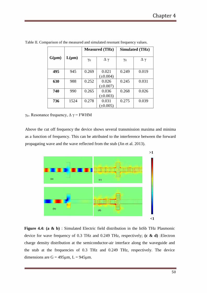
Chapter 4
50
Table II. Comparison of the measured and simulated resonant frequency values.
G(µm)
L(µm)
Measured (THz)
Simulated (THz)
γ0 Δ γ γ0 Δ γ
495
945
0.269 0.021
(±0.004)
0.249 0.019
630
988 0.252 0.026
(±0.007)
0.245 0.031
740
990
0.265 0.036
(±0.003)
0.268 0.026
736
1524
0.278 0.031
(±0.005)
0.275 0.039
γ0= Resonance frequency, Δ γ = FWHM
Above the cut off frequency the device shows several transmission maxima and minima
as a function of frequency. This can be attributed to the interference between the forward
propagating wave and the wave reflected from the stub (Jin et al. 2013).
Figure 4.4: (a & b) : Simulated Electric field distribution in the InSb THz Plasmonic
device for wave frequency of 0.3 THz and 0.249 THz, respectively; (c & d) :Electron
charge density distribution at the semiconductor-air interface along the waveguide and
the stub at the frequencies of 0.3 THz and 0.249 THz, respectively. The device
dimensions are G = 495µm, L = 945µm.
>1
<1

Chapter 4
51
Figure 4.4(a) shows the electric field distribution at a frequency of 0.3 THz and represents
maximum signal transmission. The same device shows transmission minimum at 0.249
THz as seen in figure 4.4 (b). Figure 4.4 (c and d) show the corresponding electron charge
density distribution, at the semiconductor-air interface along the waveguide and the stub,
for maximum and minimum transmission, respectively.
Figure 4.5 shows the “Transmission Map” depicting the transmission characteristics of
the device with the guided-wave frequency (in THz) and the waveguide width G (in µm)
as two parameters. The green stripes represent regions of very low signal transmission.
Thus, for G value of about 300µm, the transmission shows sharp dip at frequencies 0.226
THz (I Mode) and 0.376 THz (II Mode). At these parameters the wave electric field
increases strongly inside the stub and very little energy is transmitted out of the device. At
other frequencies the signal transmission is very high and the electric field in the stub is
negligible (Mendis et al. 2009) as is also evident from figure 4.3.
Figure 4.5: Finite element method based transmission coefficient (in dB) at THz
frequency for various gaps. This 2D image is for InSb waveguide with L= 1000 µm and G
= W with dashed lines showing the resonant modes inside the stub leading to transmission
minima.

Chapter 4
52
It is also clear from figure 4.5 that the device could be designed to operate at a chosen
resonance frequency, at which the transmission exhibits a sharp dip. Further, frequency
tunability of the device is also possible since the carrier concentration of InSb can be
altered by electrical or optical methods. This modulates the frequency dependent
permittivity of InSb leading to changes in the transmission characteristics of the device.
4.3 CONCLUSIONS
In conclusion, we have investigated experimentally the THz transmission characteristics
of InSb plasmonic waveguide devices with stubs and shown that they function as a
frequency selective filter. InSb waveguide devices were fabricated with the following
dimensions, G = 495 µm, L = 945 µm; G = 635 µm, L = 988 µm; G = 740 µm, L = 990
µm; G = 736 µm, L = 1524 µm. The transmission minimum occurred at 0.269THz,
0.252THz, 0.265THz, and 0.278THz respectively, which agree well with the simulation.
The transmission resonance dip of the device shows a shift as the width of the waveguide
G and the stub length L is varied. At those resonance frequencies there is a strong
interaction of propagating electric field E
with the stub, resulting in low signal
transmission of the device. At other frequencies the devices show high transmission. The
effect of varying G and L was studied experimentally which leads to difference in
confining the electric field inside the stub and shifts the resonance frequency. The
amplitude difference can be correlated to the coupling efficiency between the incident
THz signal and the cross sectional area of waveguide input port. Results from finite
element method simulation using COMSOL Multiphysics show similar trend in the
resonant frequency of the designed InSb waveguide device with stubs. This resonance
feature of the device was used to sense the presence of protein–water (BSA-W) mix and
Polystyrene (PS) dissolved in toluene at different concentrations. The ability of the device
to work as a sensitive biosensor is discussed in the next chapter.
CHAPTER 5
52
CHAPTER 5
InSb WAVEGUIDE DEVICES AS MATERIAL
SENSORS
Abstract
This chapter demonstrates the possibility of employing the InSb plasmonic waveguide
device, designed to operate at terahertz (THz) frequencies, for sensing materials. For a
waveguide width of 740μm and stub length of 990μm, a transmission minimum is seen to
occur at 0.265 THz. We investigated the capability of the device to sense protein
molecule Bovine serum albumin (BSA) and polystyrene, dissolved in toluene, loaded into
the stubs. The consequent change in the refractive index in the stubs alters the transmitted
signal intensity. Our results show that, a change in the concentration of the loaded sample
even by 1mol/L, leads to measurable change in the transmission coefficient close to the
resonant frequency of the device. Thus, these plasmonic devices operating at THz
frequencies show promising potential as chemical and bio sensors.
5.1 INTRODUCTION
Terahertz technologies have opened up new domains in Sensor development.
Researchers are now equipped with new tools for qualitative as well as quantitative
sensing of various materials including chemicals and biological materials. This
interest in using terahertz radiation for detecting materials is due to the fact that
radiation at these frequencies excites the vibrational and rotational energy levels in the
complex molecules, which turn out to be characteristic signatures of the molecules.
The accurate detection of chemical and biological substances in minute quantities has
been a major goal in THz sensing in the past few years. A wide variety of sensing
strategies have been developed to provide high sensitivity, reusability, portability,
miniaturization, low cost for mass production, small sample volume and ease of use.
These features constitute desirable requirements for any sensor. THz sensing devices
like PPWG (Laman et al. 2008), THz antennas (Berrier et al. 2012), split ring

CHAPTER 5
53
resonators, metamaterials (Singh et al 2014), Polymer THz fiber (You et al. 2012), are
a few of the THz devices developed for sensing applications.
Among the various options, devices having a resonant cavity have proved to be the
most promising. A Parallel Plate Wave-Guide (PPWG) with a resonant cavity,
forming a part of a lab-on-chip device, was demonstrated to function as a highly
sensitive refractive index sensor with a sensitivity of 91.25 GHz/RIU (Mendis et al
2009). A THz metamaterial device, consisting of symmetric split ring resonators, was
exploited as ultrasensitive refractive index sensor, possessing a sensitivity of 36.7
GHz/RIU and 23.9 GHz/RIU when Fano and Quadrupole resonances, respectively,
were excited (Singh et al 2014). THz antenna (Berrier et al 2012) was used to detect
bacteria with high sensitivity. These THz sensors can sense ultra-thin (a few
nanometer thick) molecular layers [John et al 2008) and a few femto-moles of DNA
molecules (Nagel et al 2002). Recently, a THz metamaterial absorber with cross
shaped elements was demonstrated as a sensor showing enhanced sensitivity
compared to planar metal-surfaces (Longqing et al 2015). Thus, resonant structures
are seen to have a big advantage over planar devices and, hence, can be integrated
with conventional electronics and other micro-sized devices to function as compact
sensor modules.
This chapter focuses on demonstrating the sensing capability of InSb Plasmonic THz
waveguide device with stub. Two types of materials, a protein and a polymer, have
been chosen for our experiments. In our Plasmonic device, as discussed in the
previous chapters, the electromagnetic waves propagate as surface waves. The other
important feature is that, the electric field of the wave, and hence, the wave energy is
strongly localized close to the semiconductor-insulator interface. This enables a
strong interaction of the wave with any material loaded into the device, leading to
significant changes in the transmission of the THz signal.
The two materials under investigation in this thesis are,
Protein - Bovine Serum Albumin (BSA)
Polymer - Polystyrene dissolved in Toluene

CHAPTER 5
54
5.2 BOVINE SERUM ALBUMIN
Bovine Serum Albumin (BSA) (Markelz et al. 2000) is a well studied protein
molecule. Hence it is chosen to study the sensing characteristics of the InSb
waveguide device. Experiments were performed to measure the THz transmission of
the device when loaded with a solution of the protein molecule BSA in deionised
water at various concentrations.
The prepared BSA-water (BSA-W) solution was dropped, using a common syringe,
into the stubs of the InSb device having dimensions W = G = 740 µm, L = 990 µm.
THz- TDS measurement was carried out as described in chapter 1 & 4.
The transmitted amplitude measured with just deionised water in the stub is
considered as the reference field amplitude Eref. Measurements were then carried out
by loading the device with 0.5mg/ml and 1mg/ml of BSA concentrations and the
measured field amplitude is Esample. Before each measurement using BSA-W sample,
transmission of THz beam in the InSb device with the empty stub and with stub filled
with deionised water (Eref) were measured to ensure consistency in the measurements.
The effective absorption coefficient (αeff) as a function of frequency (ω) of the
measured spectra was defined as (Kitagawa et al 2006),
0.0 0.2 0.4 0.6 0.8 1.06
9
12
15
18
21
Ab
so
rpti
on
co
eff
icie
nt
cm
-1
Concentration of BSA mg
0.2 0.4 0.6 0.8 1.00
5
10
15
20
Ab
so
rpti
on
co
eff
icie
nt
cm
-1
Frequency THz
Water
0.5mg/ml of BSA
1mg/ml of BSA
Figure. 5.1(a) Calculated Absorption coefficient of the BSA-Water solution, loaded into the
stub of the plasmonic device, from the normalized amplitude measured by the THz-TDS
technique. (b) Absorption coefficient versus concentration of BSA. Slope of the linear fit
gives a sensitivity of1
~ 13/
cm
mg ml
.
(a)
(b)
CHAPTER 5
55
( )1( ) ln
( )
sample
eff
ref
E
W E
(5.1)
where W (~ 740µm) is the width of the stub, called as the sensing length, Esample and
Eref are the Fourier transformed spectra corresponding to BSA and deionized water.
Figure 5.1(a) shows ( )eff calculated from the measured data when the device was
loaded first with water and next with BSA solution of concentration 0.5mg/ml and
1mg/ml. As the concentration of BSA increases, the number of absorbing water
molecules decreases for a fixed quantity of the solution, leading to decrease
in ( )eff . The observed decrease in ( )eff with the increasing concentration of the
BSA molecule is consistent with results reported (Kitagawa et al 2006, Paul et al
2008).
We determined the sensitivity of the sensor by noting the decrease in the absorption
coefficient with increasing concentration of BSA. The plot of the decrease in the
absorption coefficient, at 0.45 THz, versus the concentration of BSA is shown in the
figure 5.1(b); the graph for water corresponds to zero concentration of BSA. The data
points indicate a linear fit over the range of concentration used in our experiments.
The slope of the graph yields a sensitivity of about1
~ 13/
cm
mg ml
. Thus, a minute change
in the concentration of BSA shows prominent change in the absorption coefficient.
This characteristic of our device demonstrates the sensing capability of the device and
its potential as a biosensor.
Plasmonic stub-waveguide device sensors also show a shift in the resonance
frequency when loaded with material media. However, within the limitations of our
experiments, such frequency shifts were smaller than ~ 0.001 THz and, further
investigations are underway to explore this aspect.
5.3 POLYSTYRENE DISSOLVED IN TOULENE
Polystyrene is a polymer, widely used as a packaging material and for making
disposable containers. Such materials have promising applications in THz Optics for
making components such as lenses, windows, beam-blocks and waveguides
(Cunningham et al. 2011). Sensing characteristics of our device was investigated by

CHAPTER 5
56
filling one of the stubs with a solution of polystyrene in toluene at different
concentrations. The solutions, thus prepared, were colourless, viscous in nature and
had a refractive index almost constant in the frequency range 0.1 to 5 THz
(Cunningham et al. 2011). In our experiments, a few millilitres of the solution were
dropped into one of the two stubs in the device and the transmission of THz waves
through the device was measured.
The THz time domain signal of the device was measured (Figure.5.2 (a)) in the
following three steps in sequence
1. Measurement without filling the stubs with any liquid or sample AE
2. Measurement after filling one of the stubs (inset in Fig. III (b)) of the
waveguide with Toluene TE
3. Measurement after filling one of the stubs with the sample solution (PS)
PE
The symbols in the brackets denote the corresponding FFT spectra.
Figure.5.2 (a) Measured time-domain transmitted electric field signals for the device
loaded with polystyrene solutions (PS) at various concentrations , (b) Corresponding
computed THz transmission spectra, (c) Variation of absorption coefficient of the
samples with frequency.
(a)
(b)
(c)

CHAPTER 5
57
The transmission measurements were repeated for each sample to ensure consistency.
The quantities T AE E for pure toluene and P TE E for solution of
polystyrene at different concentrations are shown in (Figure.5.2 (b)).
Figure.5.2 (b) indicates a monotonic decrease, over a significant frequency range, in
the transmission of the THz wave with increasing concentration of polystyrene in
toluene. The effective absorption coefficient (αeff) as a function of frequency of the
measured spectra was calculated as shown in Eq. 5.1, where W ~ 750 µm is the width
of the stub.
(Figure.5.2 (c)) shows the variation of ( )eff
with frequency at different
concentrations of polystyrene, as calculated from the data shown in (Figure.5.2 (c)).
When the sample material with different permittivity was placed inside one of the
stub, the propagating THz wave experiences a dielectric loss in the stub. Due to the
resonance characteristics of our device, the change in the transmission coefficient
turns out to be very sensitive to varying concentration of polystyrene.
Figure.5.3 shows eff at 0.265 THz (for G = 740µm, L = 990µm) for different
concentrations of the solution. It is seen that absorption of the THz wave increases
with increase in the concentration of polystyrene in the solution. The sensitivity of
Figure 5.3 Absorption coefficients versus concentration of PS at the resonant
frequency of 0.265 THz showing a linear behaviour. The slope of the graph yields a
sensitivity of1
~ 2200/
cm
g ml
.

CHAPTER 5
58
our measurement, obtained from the slope of the graph, is1
~ 2200/
cm
g ml
. It is clear that,
exploiting the resonant nature of the device to enhance the wave electric field in the
stubs is a simple and a promising method to sense the presence of a minute quantity
of a polymer.
5.4 CONCLUSIONS
In conclusion, we have shown that an InSb plasmonic waveguide device can detect
the presence of minute quantity of materials with high sensitivity. Our device
functions as a resonant structure, showing minimum transmission at a particular
frequency in the THz range. Loading one of the stubs with the sample material
reduces the transmission coefficient of the device for THz waves of frequency close
to the resonant frequency. A minute change in the concentration of the solution,
changes the effective refractive index of the stub filled with the sample material.
Dissolving protein molecules in water, in bulk quantity and studying their THz
properties is a formidable task. Using only a micro litre quantity of BSA-W solution
in our device and be able to detect the BSA-W concentrations with the sensitivity
1
~ 13/
cm
mg ml
is a very substantial improvement over this problem. Similarly, the
transmitted amplitude reduces as the concentration of polystyrene in toluene increases
with the sensitivity of1
~ 2200/
cm
g ml
. Even a change of 1mol/L in the concentration can
be measured using our device. This characteristic of our device demonstrates its
sensing capability and its potential as a good sensor. The device is simple to fabricate,
has a small foot-print and it is possible to incorporate multiple plasmonic devices into
a single sensor system in a lab-on-chip environment.

Chapter 6
1
CHAPTER 6
SUMMARY AND CONCLUSIONS
6.1 THz InSb WAVEGUIDE DEVICE WITH STUB AS RESONANT
STRUCTURE
THz Plasmonic waveguide devices were designed and simulated to operate in the
frequency domain 0.1-1.0 THz.
Frequency dependent permittivity of InSb was modelled using Drude free electron
model.
COMSOL Multiphysics and Ansoft HFSS, FEM based simulation tools, were
used to solve the EM boundary value problem and to model and simulate the
designed SIS waveguide device.
The Effective Index method has been employed to study the surface plasmon
propagation in the InSb channel waveguide of sub-wavelength width.
Surface plasmon propagation and the filtering properties of InSb waveguide
device, coupled to single and two pair of stubs, which functions as a resonator at
THz frequencies were numerically studied.
These waveguide devices with stubs resonate at particular discrete frequencies
called the resonant frequencies and transmit all other frequencies.
The major change with two stub pairs is that the resonance profiles are much
sharper at the various resonant frequencies. Thus, a device with double stub pair
should be a much more sensitive filter device compared to a single stub device.
The resonant nature of the devices was proved analytically using the microwave
transmission line theory by modelling the waveguide device as an equivalent RLC
circuit following the work of Pannipitiya et al. 2010.
THz InSb waveguides were fabricated on InSb pellets using laser
micromachining.

Chapter 6
2
The transmission characteristics of the fabricated waveguide device were studied
experimentally using THz – TDS. The devices showed resonance dip and also a
shift as width of the waveguide G and the stub length L is varied.
At resonance frequencies there is a strong interaction of propagating electric field
with the material present in any stub, resulting in large changes in the
transmission coefficient of the device.
6.2 THz InSb WAVEGUIDE DEVICE AS MATERIAL SENSOR
The resonance feature of the device was exploited to study the suitability of the
device to function as a sensitive chemical sensor using (a) protein - Bovine Serum
Albumin (BSA), (b) polymer - Polystyrene dissolved in toluene as samples.
The chemicals introduced inside the stub of the InSb waveguide device altered the
permittivity of the medium, thereby changing the transmission close to the
resonant frequency of the device.
Absorption coefficient calculated from the transmission measurements clearly
indicated the presence of chemical inside the stub making InSb waveguide a
sensitive chemical sensor.
Dropping only a micro litre quantity of sample in the stub resulted in detecting
BSA concentrations with the sensitivity 1
~ 13/
cm
mg ml
and polystyrene dissolved in
toluene with the sensitivity of1
~ 2200/
cm
g ml
.
Loading one of the stubs with the sample material reduces the transmission
coefficient of the device for THz waves of frequency close to the resonant
frequency. Even a change of 1mol/L in the concentration can be measured using
this device.
Clearly InSb THz plasmonic waveguide is a simple and flexible device for sensing
application and has a possibility of incorporating multiple sensors into a single
device for a lab on chip environment.

Chapter 6
3
6.3 SCOPE FOR FUTURE WORK
The present research investigations can be further extended in the following directions,
Present investigations focused on using intrinsic semiconductor InSb for THz
plasmonic devices. This can be extended by using doped InSb, Si, Ge or other
semiconductors whose plasma frequency fall in the THz region.
Transmission characteristics of InSb waveguide device can be made tuneable by
varying the carrier concentration of InSb thermally or optically.
The studies presented here were mainly focused on InSb waveguide device with
single stub. Only simulations were carried out for double stub case. Experimental
investigations on the transmission characteristics of InSb waveguide device with
double stub pairs can be carried out.
Transmission coefficient of few more chemicals can be measured using the InSb
waveguide device to examine the suitability of the device as a chemical sensor.

References
63
REFERENCES
Auston D. H., Johnson A. M., Smith P. R., and Bean J. C. (1980). “Picosecond
optoelectronic detection, sampling, and correlation measurements in amorphous
semiconductors.” Applied Physics Letters 37, 371.
Auston D. H., Cheung K. P., and Smith P. R. (1984). “Picosecond photoconducting
Hertzian dipoles.” Applied Physics Letters 45, 284 (1984).
Barnes William L., Alain Dereux, Thomas W. Ebbesen (2003). “Surface plasmon
subwavelength optics.” Nature, Vol. 424, 824-830.
Berini P. (2000). “Plasmon-polariton waves guided by thin lossy metal films of finite
width: bound modes of symmetric structures.” J. Phys. Rev. B 61, 10484-10503.
Berini P., Stohr A., Wu K., Jager D. (1996). “Normal mode analysis and
characterization of an InGaAs/GaAs MQW field-induced optical waveguide including
electrode effects.” J. Lightwave Technology. 14, 2422-2435.
Berrier A, M. C. Schaafsma, G. Nonglaton, J. Bergquist, and J. G. Rivas (2012).
“Selective detection of bacterial layers with terahertz plasmonic antennas ”Optics
Express, 3, 11, 1–4.
Bozhevolnyi Sergey I., Valentyn S. Volkov, Eloïse Devaux, and Thomas W. Ebbesen
(2005). “Channel Plasmon-Polariton Guiding by Subwavelength Metal Grooves.”
Phys. Rev. Lett. 95, 046802.
Bozhevolnyi S.I, Davoyan A, Shadrivov I.V, , Kivshar Y.S (2010). Backward and
forward modes guided by metal-dielectric-metal plasmonic waveguides. J.
Nanophotonics. 0001;4(1):043509-043509-10.
Burton, F.A.; Cassidy, S.A. (1990). “A complete description of the dispersion relation
for thin metal film plasmon-polaritons.” J. Lightwave Technology , vol.8, no.12,
pp.1843,1849.
Chen H.T., W. J. Padilla, J. M. O. Zide, A. C. Gossard, A. J. Taylor, and R. D. Averitt
(2006).“Active terahertz metamaterial devices.” Nature 444(7119), 597–600.
Chen H.T, H. Lu, A. K. Azad, R. D. Averitt, A. C. Gossard, S. A. Trugman, J. F.
O’Hara, and A. J. Taylor (2008). “Electronic control of extraordinary terahertz
transmission through subwavelength metal hole arrays,” Opt.Express 16(11), 7641–
7648.

References
64
Chen Lin, Jiaming Xu, Chunmei Gao, Xiaofei Zang, Bin Cai, and Yiming Zhu (2013).
“Manipulating terahertz electromagnetic induced transparency through parallel plate
waveguide cavities” Applied Physics Letters 103, 251105.
Clawson R. (2001). Guide to references on III–V semiconductor chemical etching,
Materials Science and Engineering: R: Reports, Volume 31, Issues 1–6, Pages 1-438,
ISSN 0927-796X, http://dx.doi.org/10.1016/S0927-796X(00)00027-9.
Cooper E. Donald (1985). “Picosecond optoelectronic measurement of microstrip
dispersion.” Applied Physics Letters 47, 33.
Cunningham P. D., N. N. Valdes, F. A. Vallejo, L. M. Hayden, B. Polishak, X.H.
Zhou, J. Luo, A. K.Y. Jen, J. C. Williams, and R. J. Twieg (2011). “Broadband
terahertz characterization of the refractive index and absorption of some important
polymeric and organic electro-optic materials” Journal of Applied Physics, 109, 4,
043505.
Dionne J. A., Sweatlock, L. A., Atwater, H. A., Polman, A. (2005). “Planar metal
plasmon waveguides: frequency-dependent dispersion, propagation, localization, and
loss beyond the free electron model.” Physical Review B, 72 (7).
Dionne J. A., Sweatlock, L. A., Atwater, H. A., Polman, A. (2006). “Plasmon slot
waveguides: Towards chip-scale propagation with subwavelength-scale localization”
Phys. Rev. B 73, 035407.
Dragoman M and Dragoman D. (2008), “Plasmonics: Applications to nanoscale
terahertz and optical devices.” Progress in Quantum Electronics, vol. 32, no. 1, pp. 1–
41.
Ebbesen T. W, Lezec H.J, Ghaemi H.F, Thio T and Wolff P.A (1998). “Extraordinary
optical transmission through sub-wavelength hole arrays”. Nature 391, 667.
Ebbesen T. W., Degiron A, Devaux E, Linke RA, Martin-Moreno L, Garcia-Vidal
FJ, . (2002) “Beaming light from a subwavelength aperture” Science. 297 (5582):820-
822.
Exter M. van, and D. Grischkowsky (1990) “Carrier dynamics of electrons and holes
in moderately doped silicon,” Phys. Rev. B 41(17), 12140–12149.
Fattinger Ch. and Grischkowsky D. (1988). “Point source terahertz optics.” Applied
Physics Letters, 53, 1480-1482.
Gallant, A. J. and Kaliteevski, M. A. and Brand, S. and Wood, D. and Petty, M. and
Abram, R. A. and Chamberlain, J. M. (2007). “Terahertz frequency bandpass filters.”

References
65
Journal of Applied Physics, 102, 023102
Gelmont B, Parthasarathy R, Globus T, Bykhovski A, Swami N. (2008), “Terahertz
(THz) Electromagnetic Field Enhancement in Periodic Subwavelength
Structures”, Sensors Journal, IEEE , vol.8, no.6, pp.791,796.
Grigorenko A. N., Polini M. and Novoselov K. S. (2012), “Graphene plasmonics.”
Nature Photonics, 6,749–758.
Grischkowsky D. (2000) "Optoelectronic characterization of transmission lines and
waveguides by terahertz time-domain spectroscopy," IEEE Journal of Selected Topics
in Quantum Electronics, vol.6, no.6, pp.1122,1135. doi: 10.1109/2944.902161.
Hasebe, S. Kawabe, H. Matsui, and H. Tabata (2012). “Metallic mesh-based terahertz
biosensing of single- and double-stranded DNA,” J. Appl. Phys, 112, 094702.
Heinz Raether (1988). “Surface Plasmons on smooth and rough surfaces on Gratings.”
Springer-Verlag Tracts in Modern Physics, volume 111 New York.
Hendry E., F. J. Garcia-Vidal, L. Martin-Moreno, J. Gómez Rivas, M. Bonn, A. P.
Hibbins, and M. J. Lockyear (2008). “Optical control over surface plasmon polariton-
assisted THz transmission through a slit aperture,” Phys. Rev. Lett. 100(12), 123901
Hocker G. B. and Burns W. K. (1977). “Mode dispersion in diffused channel
waveguides by the effective index method.” Appl. Opt. 16, 113-118.
Isaac T. H., Rivas J. Gómez, Sambles J. R., Barnes W. L., and Hendry E. (2008).
“Surface plasmon mediated transmission of subwavelength slits at THz frequencies”
Phys. Rev. B 77, 113411.
Jin Tao, Bin Hu, Xiao Yong He, Qi Jie Wang (2013). “Tunable Subwavelength
Terahertz Plasmonic Stub Waveguide Filters” IEEE Transactions on
Nanotechnology, 12, 6, 1191-1197.
John F. O'Hara, Ranjan Singh, Igal Brener, Evgenya Smirnova, Jiaguang Han,
Antoinette J. Taylor, and Weili Zhang, (2008). "Thin-film sensing with planar terahertz
metamaterials: sensitivity and limitations," Optics. Express 16, 1786-1795.
Keiser G. (1991). Optical Fiber Communications, McGraw-Hill, 1991.
Kimberly S. Reichel, Krzysztof Iwaszczuk, Peter U. Jepsen, Rajind Mendis, and
Daniel M. Mittleman (2014). “In situ spectroscopic characterization of a terahertz
resonant cavity”, Optica 1, 272-275.
Kitagawa, J. and Ohkubo, T. and Onuma, M. and Kadoya Y. (2006). “THz
spectroscopic characterization of biomolecule/water systems by compact sensor
chips.” Appl. Phys. Lett. 89, 041114.

References
66
Knox R.M. and P.P. Toulios (1970). “Integrated circuits for millimetre through optical
frequency range.” Edited Fox J., Ed., Proc. MRI Symposium on sub millimetre waves,
Brooklyn 497-516.
Koichiro Ueno, Edson Gomes Camargo, Takashi Katsumata, Hiromasa Goto, Naohiro
Kuze, Yoshihiro Kangawa and Koichi Kakimoto (2013). “InSb Mid-Infrared Photon
Detector for Room-Temperature Operation” Jpn. J. Appl.
Phys. 52 092202 doi:10.7567/JJAP.52.092202.
Kretschmann E. and Raether. H (1968). “Radiative Decay of Non Radiative Surface
Plasmons Excited by Light.” Zeit.fur Naturforschung, 23a, 2135-2136.
Kumar G., S. Pandey, A. Cui, and A. Nahata (2011). “Planar plasmonic terahertz
waveguides based on periodically corrugated metal films” New Journal of Physics, 13,
3, 033024.
Laman. N, S. S. Harsha, D. Grischkowsky, and J. S. Melinger (2008). “High
Resolution Waveguide THz Spectroscopy of Biological Molecules”, Biophysical
Journal, 94, 3, 1010–1020.
Lamprecht B., Krenn J.R., Schider G., Ditlbacher H., Salerno M., Felidj N., Leitner
A., Aussenegg F. R., Weeber J.C. (2001). “Surface plasmon propagation in microscale
metal stripe.” Applied Physics Letters, Vol. 79, No. 1.
Lo Shu-Zee A. and Murphy Thomas E (2010), “Terahertz surface plasmon propagation
in nanoporous silicon layers”, Applied Physics Letters, 96, 201104.
Longqing Cong, Siyu Tan, Riad Yahiaoui, Fengping Yan, Weili Zhang, and Ranjan
Singh (2015). “Experimental demonstration of ultrasensitive sensing with terahertz
metamaterial absorbers: A comparison with the metasurfaces.” Appl. Phy Letts, 106,
031107.
Marti O., Bielefeldt H., Hecht B., Herminghaus S., Leiderer P., Mlynek J.(1993).
“Near-field optical measurement of the surface plasmon field, Optics
Communications.” Volume 96, Issues 4–6, 15 Pages 225-228.
Markelz A.G., A Roitberg, E.J Heilweil (2000). “Pulsed terahertz spectroscopy of
DNA, bovine serum albumin and collagen between 0.1 and 2.0 THz” Chemical Physics
Letters, 320, 1–2, 31.
Matsuzaki, T. Okamoto, M. Haraguchi, M. Fukui, and M. Nakagaki (2008).
“Characteristics of gap plasmon waveguide with stub structures,” Opt. Express 16,
16314-16325.

References
67
Masayoshi Tonouchi (2007). “Cutting-edge terahertz technology.” Nature Photonics 1,
97 – 105.
McGowan R. W. and Grischkowsky D. (1999). “Experimental time-domain study of
THz signals from impulse excitation of a horizontal surface dipole.” Applied Physics
Letters, 74, 1764-1766 (1999)
Mendis R, V. Astley, J. Liu, and D. M. Mittleman (2009), “Terahertz microfluidic
sensor based on a parallel-plate waveguide resonant cavity”, Applied Physics Letters,
vol. 95, no. 17, p. 171113.
Nagel M., Haring Bolivar P., M. Brucherseifer, H. Kurz, A. Bosserhoff, and R.
Büttner (2002). “Integrated THz technology for label-free genetic diagnostics.” Appl.
Phys. Lett. 80(1), 154– 156.
Pannipitiya Asanka, Rukhlenko D. Ivan, Premaratne Malin, Hattori T. Haroldo, and.
Agrawal P. Govind P. (2010). “Improved transmission model for metal-dielectric-metal
plasmonic waveguides with stub structure.” Optics Express 18, 6191-6204.
Paul A. George, Christina Manolatou, Farhan Rana. Adam L. Bingham and Daniel R.
Grischkowsky (2007). “Integrated waveguide-coupled terahertz microcavity
resonators.” Appl. Phys. Lett. , 91, 191122.
Paul A. George,Wallace Hui, FarhanRana, Benjamin G. Hawkins, A. Ezekiel Smith,
Brian J. Kirby (2008). “Microfluidic devices for terahertz spectroscopy of
biomolecules.” Optics Express, 16, 3, 16314-16325.
Paul Drude (1900). “Zur Elektronentheorie der metalle.”. Annals of Physics, 1, 566-
613.
Pedry J (2000). “Negative Refraction Makes a Perfect Lens.” Physical Review Letter.
85, 39663969.
Pendry J., Krishnan, T Thio, T.J Kim, H.J Lezec, T.W Ebbesen, P.A Wolff, L Martin-
Moreno, F.J Garcia-Vidal (2001). “Evanescently coupled resonance in surface plasmon
enhanced transmission. Optics Communications, Volume 200, Issues 1–6, Pages 1-7.
Pozar D. M, Microwave Engineering, 2nd ed. (Wiley, New York, 1998).
Prade B., Vinet J. Y., Mysyrowicz A. (1991). “Guided optical waves in planar
heterostructures with negative dielectric constant.” Phys. Rev. B 44, 13556–13572.
Reichel K., Iwaszczuk K., Jepsen P., Mendis R., and D. Mittleman (2014), “In situ
spectroscopic characterization of a terahertz resonant cavity”Optica 1, 272-275.
Ritchie (1957). “Plasma Losses by Fast Electrons in Thin Films.” Phy.Rev, 106(5),
874-881.

References
68
Rivas J. G, P. H. Bolivar, and H. Kurz (2004), “Thermal switching of the enhanced
transmission of terahertz radiation through sub-wavelength apertures,” Opt. Lett.
29(14), 1680–1682.
Sambles R., Bradbery G. W and Fuzi Yang (1991). “Optical excitation of surface
plasmons: An introduction.” Contemporary Physics Volume 32, Issue 3, pages 173-
183
Singh Ranjan, Wei Cao, Ibraheem Al-Naib, Longqing Cong, Withawat
Withayachumnankul, and Weili Zhang (2014). “Ultrasensitive terahertz sensing with
high-Q Fano resonances in metasurfaces”, Applied Physics Letters, 105,171101.
Sommerfeld A. (1899), “Ueber die Forpflanzung elektrodynamischer Wellen langs
eines Drahtes.” Ann. Phys. U. Chem., 67, 233-290.
Stefan A Maier (2006).’Plasmonics: Fundamentals and Applications.’ Springer-
verlag, New York.
Stefan A Maier (2012). “Graphene plasmonics: All eyes on flatland.” Nature Physics
8, 581–582
Steven R Andrews (2014) “Microstructured terahertz waveguides” J. Phys. D: Appl.
Phys. 47 374004. doi:10.1088/0022-3727/47/37/374004
Takahara J., Yamagishi S., Taki H., Morimoto A., Kobayashi T.(1997). “Guiding of a
one-dimensional optical beam with nanometer diameter” Optics Letter 22, 475477.
Tournois Pierre, Laude Vincent (1997). “Negative group velocities in metal-film
optical waveguides, Optics Communications.” Volume 137, Issues 1–3, 15, Pages 41-
45.
Vakil, A., Engheta, N. (2011). “Transformation Optics Using Graphene.” Science 332,
1291–1294.
Veronis G. and Shanhui Fan (2005), “Bends and splitters in metal-dielectric-metal
subwavelength plasmonic waveguides,” Appl. Phys. Lett. 87, 131102(1-3).
Veronis, G. Shanhui Fan (2007). “Modes of Subwavelength Plasmonic Slot
Waveguides.” J. Lightwave Technology, vol.25, no.9, pp.2511-2521.
Vincenzo Giannini, Berrier A., Maier S. A., Sánchez-gil J. A., and J. G. Rivas J. A.
(2010), “Scattering efficiency and near field enhancement of active semiconductor
plasmonic antennas at terahertz frequencies” Optics Express, 18, 3, 7028–7034.
Wächter Markus, Michael Nagel, and Heinrich Kurz, (2007). “Metallic slit waveguide
for dispersion-free low-loss terahertz signal transmission” Applied Physics Letters 90,
061111; doi: 10.1063/1.2472544.
References
69
Weeber J.C., Krenn J. R., Dereux A., Lamprecht B., Lacroute Y., and. Goudonnet J. P
(2001). “Near-field observation of surface plasmon polariton propagation on thin
metal stripes”, Phys. Rev. B, 64, 045411.
Yang Hongyan, Li Jianqing, Xiao Gongli (2014). “A highly efficient surface plasmon
polaritons excitation achieved with a metalcoupled metal-insulator-metal waveguide”
AIP Advances 4, 127114.
You B, J.-Y. Lu, C.-P. Yu, T.-A. Liu, and J.-L. Peng. (2012). “Terahertz refractive
index sensors using dielectric pipe waveguides.,” Optics express, vol. 20, no. 6, pp.
5858–66.
Zenneck J. (1907). “Fortplafanzung ebener elektromagnetischer Wellen lands einer
ebenen Leiterflache.”, Ann. D. Phys., 23, 846-866.
Zhan Hui, Rajind Mendis, and Daniel M. Mittleman (2011). “Characterization of the
terahertz near-field output of parallel-plate waveguides”, J. Opt. Soc. Am. B, 28, 558-
566
Zhu X. L., Yan W., Mortensen N. A. & Xiao S. S. (2013). “Bends and splitters in
graphene nanoribbon waveguides.” Optics Express, 21, 3486–3491.
Zhu. W, A. Agrawal, A. Cui, G. Kumar, and A. Nahata (2011). “Engineering the
Propagation Properties of Planar Plasmonic Terahertz Waveguides”, IEEE Journal of
Selected Topics in Quantum Electronics, vol. 17, no. 1, pp. 146–153.
Zia Rashid, Selker Mark D., Catrysse Peter B., and Brongersma Mark L. (2004).
"Geometries and materials for subwavelength surface plasmon modes." J. Opt. Soc.
Am. A 21, 2442-2446.
Zheng Jiajiu, Longhai Yu, Sailing He Daoxin Dai (2015). “Tunable pattern-free
graphene nanoplasmonic waveguides on trenched silicon substrate”, Scientific Reports
5, Article No. 7987, doi:10.1038/srep07987.

Publications
70
LIST OF PUBLICATIONS
(A) Research papers in International Journals
1 Shourie Ranjana J, Piyush Bhatt, Harshad Surdi, Bagvanth Sangala, M.N, Satyanarayan,
G, Umesh, S S, Prabhu (2016), “Resonant Terahertz InSb Plasmonic Waveguide Device
for Sensing Polymers ” – Journal of Infrared Millimeter and Terahertz wave, Springer
Publications 10.1007/s10762-016-0268-7.
2 Shourie Ranjana J, Piyush Bhatt, Harshad Surdi, Bagvanth Sangala, M.N, Satyanarayan,
G, Umesh, S S, Prabhu (2015), “Bio-interfacing of resonant transmission characteristics of
InSb based Terahertz Plasmonic waveguide” – Biomed. Phys. Eng. Express 1 025003
doi:10.1088/2057-1976/1/2/025003
(B) Research papers in International conferences
1 Shourie Ranjana J, Bhatt P, Surdi H, Sangala B.R, Satyanarayan M.N, Umesh G, Prabhu
S.S (2015), "Indium Antimonide (InSb) waveguide based THz sensor," 2015 IRMMW,
University of Hong Kong, IEEE Conf. Proceedings. 10.1109/IRMMW-
THz.2015.7327917.
2 Shourie Ranjana J, Bhatt P, Surdi H, Sangala B.R, Satyanarayan M.N, Umesh G, Prabhu
S.S (2014), "Indium Antimonide (InSb) based planar terahertz plasmonic
waveguide," IEEE Conf. Proc, DOI: 10.1109/IRMMW-THz.2014.6956437
3 Shourie Ranjana J, M. N. Satyanarayan and G. Umesh (2013). Indium Antimonide
(InSb) Cavity Resonators based on Planar Plasmonic Terahertz Waveguide. MRS
Proceedings, 1566, mrss13-1566-ii09-19 DOI:10.1557/opl.2013.944.
4 Shourie Ranjana J., M. N. Satyanarayan, G. Umesh, (2014). “Indium Antimonide (InSb)
based Planar Terahertz Plasmonic Cavity Resonator as Biosensors” 2014 International
Conference of Optics and Optoelectronics, XXXVIII Symbosium of optical society of
India. 5th March to 8th March 2014, Dehradun, Uttarkhand, INDIA.
5 Shourie Ranjana J, M. N. Satyanarayan, G. Umesh, (2011). “Surface Plasmon
Propagation on Metal Insulator Metal (MIM) waveguide: Simulation Studies”, Recent
Trends in Nanophotonics” 30th Sep to 1st Oct 2011, IIT Delhi, INDIA.

Curriculum Vitae
71
17, Chinnasamy Pillai Street, Bethaniapuram
Madurai – 625016, Tamilnadu
India
Ph: 09008909165
SHOURIE RANJANA J
EDUCATION
Ph.D in Physics (THz Plasmonics)
Title: “Investigations on InSb plasmonic devices for sensor applications at Terahertz
frequencies”
Institute: NITK Surathkal, Mangalore, INDIA.
Advisor: Prof. G. Umesh and Dr. M.N. Satyanarayan
Year: Thesis submitted (October 2015)
M.Sc. Physics [2008 - 10]
NITK Surathkal, Mangalore, INDIA.
B.Sc. Physics [2005 - 08]
Madurai Kamarajar University, Lady Doak College, Madurai, INDIA.
HIGHLIGHTS
Excellent academic record (CP1 ~8.5/10)
Expertise in performing electromagnetic simulations.
Expertise in simulation, fabrication and characterization of Terahertz (THz) and optical
waveguide, resonators and filter at, NITK Surathkal, IITBNF in IIT Bombay and TIFR
Mumbai.
RESEARCH INTEREST
Novel electromagnetic devices for future technology
Fabricate and characterize integrated electromagnetic devices with lab on chip
environment.
New materials for electromagnetic device applications.

Curriculum Vitae
72
RESEARCH EXPERTISE
THz planar plasmonic Indium Antimonide (InSb) waveguides (PhD).
Design and Simulate THz plasmonic waveguide using COMSOL®
Multiphysics as a
resonant structure using InSb. Including modelling the frequency dependent property
of InSb.
Fabrication of InSb pellets and laser micromachining of InSb THz waveguides.
Characterization of InSb waveguide using standard terahertz time domain spectroscopy
in transmission mode (THz-TDS) in determining the resonant nature of the device.
Testing the InSb waveguide with bio chemical samples like proteins, blood serum and
polymer to monitor its function as a sensitive chemical sensor.
Fabrication of SU8 based multimode optical waveguides and ring resonators (MSc).
Design and simulate SU8 based optical waveguide and ring resonators using RSOFT
Beamprob for multimode operation.
Fabricate waveguide and resonators using spin coating and basic lithography technique
in semi clean room environment.
Third order nonlinear optical studies of polymer doped organic molecules(MSc).
Fabricate PMMA doped with third order nonlinear organic molecule, thin films using
spin coating technique on glass substrates.
Characterize the thin films using Z-Scan technique and study the optical limiting
property of the films.
TECHANICAL SKILLS
Developed technical expertise in simulation and fabrication of THz devices during my PhD
through working in NITK Surathkal, Nanofabricatoin lab in IIT Bombay and TIFR, Mumbai
Simulation Skills: RF simulation in COMSOL® Multiphysics, Ansoft HFSS, CST
Microwave Studio, BeamProb Rsoft, MEEP- FDTD.
Fabrication Skills: Laser ablation and micromachining using ND: YAG laser,
Thermal evaporation, Pulsed laser deposition, Spin coating technique, Basic optical
lithography.
Characterization Skill: THz TDS, Z-Scan, UV absorption spectroscopy, Electrical
characterization (IV, CV) using Cascade Probe station.
Expertise in designing, setting up and handling optical and THz measurements.

Curriculum Vitae
73
Expertise in writing of scientific and technical papers and documentations.
WORK EXPERIENCE
Teaching Assistant in Department of Physics, NITK – Teaching different courses on
Electromagnetic theory and Engineering Physics at under graduate and post graduate
level (July 2010 – present)
LIST OF PUBLICATIONS
1 Shourie Ranjana J, Piyush Bhatt, Harshad Surdi, Bagvanth Sangala, M.N, Satyanarayan, G,
Umesh, S S, Prabhu (2016), “Resonant Terahertz InSb Plasmonic Waveguide Device for
Sensing Polymers ” – Journal of Infrared Millimeter and Terahertz wave, Springer Publications
10.1007/s10762-016-0268-7.
2 Shourie Ranjana J, Piyush Bhatt, Harshad Surdi, Bagvanth Sangala, M.N, Satyanarayan, G,
Umesh, S S, Prabhu (2015), “Bio-interfacing of resonant transmission characteristics of InSb
based Terahertz Plasmonic waveguide” – Biomed. Phys. Eng. Express 1 025003
doi:10.1088/2057-1976/1/2/025003
CONFERENCE PROCEEDINGS
1 Shourie Ranjana J, Bhatt P, Surdi H, Sangala B.R, Satyanarayan M.N, Umesh G, Prabhu S.S
(2015), "Indium Antimonide (InSb) waveguide based THz sensor," 2015 IRMMW, University
of Hong Kong, IEEE Conf. Proceedings. 10.1109/IRMMW-THz.2015.7327917
2 Shourie Ranjana J, Bhatt P, Surdi H, Sangala B.R, Satyanarayan M.N, Umesh G, Prabhu S.S
(2014), "Indium Antimonide (InSb) based planar terahertz plasmonic waveguide," IEEE Conf.
Proc, DOI: 10.1109/IRMMW-THz.2014.6956437
3 Shourie Ranjana J, M. N. Satyanarayan and G. Umesh (2013). Indium Antimonide (InSb)
Cavity Resonators based on Planar Plasmonic Terahertz Waveguide. MRS Proceedings, 1566,
mrss13-1566-ii09-19 DOI:10.1557/opl.2013.944.
4 Shourie Ranjana J., M. N. Satyanarayan, G. Umesh, (2014). “Indium Antimonide (InSb)
based Planar Terahertz Plasmonic Cavity Resonator as Biosensors” 2014 International
Conference of Optics and Optoelectronics, XXXVIII Symbosium of optical society of India. 5th
March to 8th March 2014, Dehradun, Uttarkhand, INDIA.
5 Shourie Ranjana J, M. N. Satyanarayan, G. Umesh, (2011). “Surface Plasmon Propagation on
Metal Insulator Metal (MIM) waveguide: Simulation Studies”, Recent Trends in
Nanophotonics” 30th Sep to 1st Oct 2011, IIT Delhi, INDIA.

Curriculum Vitae
74
AWARDS
National award for First prize in Indian National Physics talent quest 2008 organized
by Indian Physics association, Mumbai.
REFERENCES
Prof. G. Umesh, [email protected], Department of Physics, NITK Surathkal
Dr. M. N. Satyanarayan, [email protected], Department of Physics, NITK
Surathkal
Prof. S. S. Prabhu, [email protected], DCMPMS, TIFR, Mumbai
PERSONAL DETAILS
Date of birth : 2nd
July 1987
Gender : Female
Father’s Name : Jebamalaidass A.
Mother’s Name : Maria Madalene A.
Nationality : Indian
Mother tongue : Tamil
Home Town : Madurai, Tamilnadu, INDIA
Language known : English, Tamil, Kannada
DECLARATION
I hereby declare that the details furnished above are true and unbiased to the best of my
knowledge.
SHOURIE RANJANA J.
Place: Surathkal, Karnataka


![InSb, ) InAsSb InSb. II 32advance.orion-ir.ru/UPF-17/3/UPF-5-3-271.pdfного» InSb, ЭС InSb, ЭС InAsSb и nBn-бариода на InAsSb [23]. В области низких](https://static.cupdf.com/doc/110x72/5f63839e4bcb9c59cf1945e8/insb-inassb-insb-ii-insb-insb-inassb-nbn-.jpg)


![Enhancing the Angular Sensitivity of Plasmonic Sensors ...biotheory.phys.cwru.edu/PDF/AOM.pdf · ultrasensitive plasmonic biosensors.[29,30] A plasmonic nanorod metamaterial (Type](https://static.cupdf.com/doc/110x72/5fcdd2c6db367d06a677e7be/enhancing-the-angular-sensitivity-of-plasmonic-sensors-ultrasensitive-plasmonic.jpg)


![Strained -Sn on InSb(001) · InSb, is likewise a heteroepitaxial strained system. The use of InSb as a template for high quality crystals is well established [18{20]. It induces a](https://static.cupdf.com/doc/110x72/5f63835e50764f10ad37eb67/strained-sn-on-insb001-insb-is-likewise-a-heteroepitaxial-strained-system-the.jpg)


