Electronic structure and transport properties of sulfur-passivated graphenenanoribbonsBikash Mandal, Sunandan Sarkar, Anup Pramanik, and Pranab Sarkar Citation: J. Appl. Phys. 112, 113710 (2012); doi: 10.1063/1.4768524 View online: http://dx.doi.org/10.1063/1.4768524 View Table of Contents: http://jap.aip.org/resource/1/JAPIAU/v112/i11 Published by the American Institute of Physics. Related ArticlesElectron-state engineering of bilayer graphene by ionic molecules Appl. Phys. Lett. 101, 233106 (2012) Response to “Comment on ‘Chiral tunneling in trilayer graphene’” [ Appl. Phys. Lett. 101, 226101 (2012)] Appl. Phys. Lett. 101, 226102 (2012) Communication: Oscillated band gaps of B/N-codoped α-graphyne J. Chem. Phys. 137, 201101 (2012) Oscillating magnetocaloric effect on graphenes Appl. Phys. Lett. 101, 222405 (2012) A graphene composed of pentagons and octagons AIP Advances 2, 042147 (2012) Additional information on J. Appl. Phys.Journal Homepage: http://jap.aip.org/ Journal Information: http://jap.aip.org/about/about_the_journal Top downloads: http://jap.aip.org/features/most_downloaded Information for Authors: http://jap.aip.org/authors
Downloaded 07 Dec 2012 to 14.139.211.2. Redistribution subject to AIP license or copyright; see http://jap.aip.org/about/rights_and_permissions
Electronic structure and transport properties of sulfur-passivatedgraphene nanoribbons
Bikash Mandal, Sunandan Sarkar, Anup Pramanik, and Pranab Sarkara)
Department of Chemistry, Visva-Bharati University, Santiniketan 731235, India
(Received 5 October 2012; accepted 6 November 2012; published online 7 December 2012)
Electronic structure of newly synthesized sulfur-terminated graphene nanoribbons (S-GNRs) has been
presented from the calculations based on ab initio density functional theory and non-equilibrium
Green’s function (NEGF) method. The calculations reveal that zigzag-edged S-GNRs (Z-S-GNRs)
are thermodynamically more stable than armchair edged S-GNRs (A-S-GNRs). It has been observed
that the band gap of S-GNRs depends both on ribbon width and edge symmetry. The calculated band
gap, in case of A-S-GNRs, is also supported by the presence of threshold bias in the I-V
characteristics obtained from NEGF formalism. It is shown that all A-S-GNRs having width up to
1.50 nm are semiconducting but the Z-S-GNRs of similar widths are metallic. For A-S-GNRs, the
width dependent band-gap hierarchy follows three different trends which seem to be different from
that of H-passivated GNRs. The band-gaps for A-S-GNRs arise from both quantum confinement as
well as crucial effect of edge, where the passivating S atoms play an important role. Band-gap may be
further tuned by introducing other passivating atoms like Se and Te. The semiconducting ribbons,
when attached to doped metallic ribbons, show negative differential resistance phenomena as
indicated by the observed I-V characteristics. VC 2012 American Institute of Physics.
[http://dx.doi.org/10.1063/1.4768524]
I. INTRODUCTION
In spite of unique electronic and physical properties of
graphene,1 its application in electronic devices is limited due
to lack of band-gap. However, the problem is resolved by
forming one dimensional nano-strips of fixed width, naming
graphene nanoribbons (GNRs),2–14 thereby introducing
band-gap in it. Furthermore, the discovery, that the band-gap
is tunable by altering the edge structure and width,2–4,7–14
opens the new age of modern semiconducting materials. The
electronic band structure of GNRs has been subject of great
interest for a long time so as to determine the optical and
transport properties of it. Graphene nanoribons show distinct
electronic properties depending upon the edge symmetry of
it.4,5 Armchair GNRs (A-GNRs) are found to be more stable
than zigzag-edged GNRs (Z-GNRs).15
Z-GNRs exhibit metallic character in ferromagnetic
state and semiconducting in antiferromagnetic ground state,
the energy difference between those two states, however, in
the order of few meV per edge atom.10 The ground-state spin
polarization may be attributed to the localization of the con-
duction bands at the edges which can also be modulated with
a transverse electric field, applied perpendicular to the rib-
bon’s axis, resulting half metalicity of the ribbons. On the
other hand, high level density functional theory (DFT) calcu-
lations predict that all armchair graphene nanoribbons
(A-GNRs) are semiconductors11–13,16,17 with different
energy gaps depending upon the width of the ribbons,
although, tight binding (TB) calculations demonstrate 3-fold
periodic pattern in band-gap variation with every third
ribbon width showing a metallic character.18 It has been
shown that the origin of energy gaps for A-GNRs arises from
both quantum confinement and crucial effect of the edges.
The band-gap of A-GNR is inversely proportional to its
width. Based on first principle calculations, Son et al.11 show
that the band-gap (D) as a function of ribbon width (Na) fol-
lows three different series with a gap size hierarchy,
D3nþ1 > D3n > D3nþ2, where Na measures the number of
dimer lines across the ribbon width and n is a positive
integer.
The possibility of edge passivation of graphene nanorib-
bon by sulfur atoms has recently been proved in laboratory.19
The selective affinity of the nanoribbons to sulfur atoms was
also confirmed by energy dispersive X-ray spectroscopy.
Chamberlain et al.,20 both by experimental and theoretical cal-
culation, show that the thermodynamic stability of nanoribbons
is dependent on the S-GNR edge structure, and to a lesser
extent, the width of the ribbon. According to them,
for nanoribbons of similar widths, the polythiaperipolycene-
type edges of zigzag S-GNRs are more stable than the
polythiophene-type edges of armchair S-GNRs. Both the edge
structure and the width define the electronic properties of
S-GNRs which can vary widely from metallic to semiconduc-
tor to insulator. Their DFT calculations show that the elec-
tronic band structures for the different S-GNRs vary
dramatically from semiconductor in the case of Z-S-GNRs to
metallic to insulator for the A-S-GNRs, depending on the
nanoribbon width. On the basis of their generalized gradient
approximation (GGA)-Perdew-Burke-Ernzerhof (PBE) results,
the authors20 have demonstrated that 4-A-S-GNR is metallic
which creates an open debate whether hopping integrals
between edge atoms11 are capable of opening the band-gap for
A-S-GNRs or not. Very recently,21 dispersion-corrected
a)Author to whom correspondence should be addressed. E-mail: pranab.
0021-8979/2012/112(11)/113710/6/$30.00 VC 2012 American Institute of Physics112, 113710-1
JOURNAL OF APPLIED PHYSICS 112, 113710 (2012)
Downloaded 07 Dec 2012 to 14.139.211.2. Redistribution subject to AIP license or copyright; see http://jap.aip.org/about/rights_and_permissions
density functional theory has been applied to investigate the
structure and electronic properties of S-GNRs encapsulated in
carbon nanotube. Their hybrid DFT calculations demonstrate
that unlike H- and O-GNRs, the S-GNR with zigzag edge is
metallic even when deformed inside carbon nanotubes.
In this paper we present the geometry and detailed elec-
tronic structure of recently synthesized sulfur-terminated
A-GNRs with different widths on the basis of systematic abinitio density functional theory within GG approximation
using PBE exchange functional. The variation of band-gap
with increasing ribbon width is also explored. The calcula-
tions reveal that the trend of band-gap variation for
S-terminated ribbon appears to be different from that of
H-terminated one. The tunable electronic properties shown
by S-GNRs may make them highly versatile 1D materials
with promising potential applications in electronic and opti-
cal devices. As for example, the semiconducting ribbons are
when attached to metallic leads, they show negative differen-
tial resistance (NDR) behavior in certain bias windows.22–24
Much efforts have been devoted for modeling new NDR
devices by means of structural modulation or by introducing
foreign elements25–27 into GNRs which may have potential
application in logic circuit, switching, amplification as well
as in memory storage. So, we wish to extend our research for
studying quantum conductance behavior of the A-S-GNRs
sandwiched in between metallic leads.
The paper is arranged as follows. A brief computational
description is made in Sec. II. Section III starts with the
results of relative thermodynamic stability. In the later part
we describe the band structure and general trends of band-
gap variation. Following this section, we present the trans-
port properties showing I-V characteristics with different
leads. Finally, conclusive remarks are drawn in Sec. IV.
II. METHOD OF COMPUTATION
Geometry relaxations and electronic structure calcula-
tions were performed using a double-f plus polarization
function (DZP) basis set and norm-conservative Troullier-
Martins pseudo-potentials (PP)28 for representing the valence
and inner electrons as implemented in SIESTA package.29 A
real space mesh cutoff of 300 Ry has been used throughout
the entire calculation. The exchange-correlation functional
of the GGA is represented by the PBE approximation.30 The
convergence criteria for the density matrix are taken as 10�4.
The conjugate gradient method is used to relax all the atoms
until the maximum absolute force was less than 0.001 eV/A.
The k-point sampling was done with 1� 1� 15 Monkhorst-
Pack k-points.
A set of transport properties were calculated using
TranSIESTA module within the SIESTA package, which is
based on the combination of density functional theory and
non-equilibrium Green’s function (NEGF) method.31,32 The
generalized gradient approximation in the PBE form is
employed for the exchange correlation functional. We used
similar basis and convergence criteria as was implemented
during geometry optimization. In the NEGF self-consistent
loop, the charge density was integrated over 400 energy
points along the semicircle in the complex plane. We used
undoped or doped ribbons as left and right electrodes thereby
sandwiching the central scattering region (SR) and current
was calculated from the Landauer-Buttiker formula, accord-
ing to which the current I(Vb) is given by
IðVbÞ ¼2e
h
ð1�1
TðE;VbÞ½fLðE� lLÞ � fRðE� lRÞ�dE; (1)
where T(E;Vb) being transmission function, fLðRÞ is the
Fermi-Dirac distribution function for left (right) lead, and
lLðRÞ is the electrochemical potential of the left (right) lead
such that eVb ¼ lL � lR.
III. RESULTS AND DISCUSSION
First, we optimize the lattice constants of 2D graphene
sheet and those of the sulfur terminated Z-GNRs and
A-GNRs of different width. Here, it should be pointed out
that, following the previous convention10,11 we also classify
Na-A-GNR and Nz-Z-GNR of different width, where Na is
the number of dimer lines (or equivalent to number of C
atoms in a zigzag chain) across the A-GNR width and Nz is
the number of zigzag chains across the Z-GNR width. Table I
displays the optimized lattice constants and relative stability
of various ribbons with different edge structures, where the
free energy of formation of a species (DGf ) is defined by
DGf ¼ ls �P
le, s and e denoting the particular species
and constituting elements, respectively. We wish to mention
here that, for representing elemental C, H, and S we consid-
ered two-dimensional graphene sheet, free H2 molecule, and
S8 molecule, respectively. It is significant to note that unlike
hydrogen-terminated ribbons, sulfur-terminated Z-GNRs are
energetically more stable than A-GNRs of similar width,
however, in any case these are more stable than the bare rib-
bon as indicated by the table. The extra stability gained by
the S-terminated ribbons in comparison to the bare ribbons
may easily be understood on the basis of saturation of valen-
cies. On the other hand, the favored perpendicular orienta-
tion of unhybridised p orbitals of S atom is reflected by the
greater stability of the S-terminated zigzag ribbons. In case
of A-GNRs the S atoms suffer from angle strain where the p
orbitals are inclined with an C-S-C angle of �968. As shown
in Table I, the optimized lattice constant of A-GNRs gradu-
ally increases with increasing the ribbon width, of course,
TABLE I. Optimized lattice constant and free energy of formation of some
nanoribbons of different edge symmetry and passivation.
Ribbon L.C. (A) DGf (eV/atom)
Zigzag C8S4 4.95 0.0878
S12S4 4.95 0.0657
C16S4 4.95 0.0529
C12H4 4.95 0.0367
C12 4.94 1.0231
Armchair C8S2 4.05 0.2255
C12S2 4.12 0.1740
C16S2 4.16 0.1473
C12H4 4.33 �0.0029
C12 4.39 0.8016
113710-2 Mandal et al. J. Appl. Phys. 112, 113710 (2012)
Downloaded 07 Dec 2012 to 14.139.211.2. Redistribution subject to AIP license or copyright; see http://jap.aip.org/about/rights_and_permissions
with a nonlinear trend. Table I also indicates that sulfur pas-
sivated ribbons are relatively less stable than hydrogen passi-
vated one, but the energy of destabilization is only 0.02 eV/
atom for the width of 0.65 nm. So, from the thermodynamic
point of view S-terminated ribbons are comparable with H-
terminated one. Fig. 1 displays optimized geometry of arm-
chair and zigzag edged S-terminated ribbons. Although our
results qualitatively resemble the previous calculation of
Chamberlian et al.,20 the values of DGf are much lower than
previously reported values. However, no experimental result
is available for comparison.
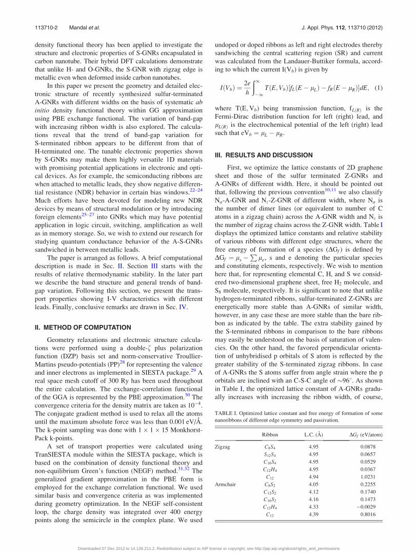
Next, to have an insight into the electronic structure of
the S-passivated ribbons, we have performed band structure
calculations of them in the same level of theory. The calcula-
tions reveal that the narrowest A-GNR (3-A-GNR) in our
calculation has the highest band-gap of 1.88 eV effectively
making it a semiconductor. With increasing ribbon width the
overall variation of band gap appears zigzag, but a closer ob-
servation indicates a regular decreasing trend of three sepa-
rate series namely, Na¼ 3n, 3nþ 1, and 3nþ 2, where n is
having positive integral values. We wish to mention here
that, while defining ribbon width, we consider C-C perpen-
dicular distance across the periodic direction as in the case
of A-H-GNRs. As shown in Fig. 2, for a particular value of
n, the 3n series has the highest band gap and the 3nþ 1 series
has the lowest one with a general trend of band gap variation
as D3n > D3nþ2 > D3nþ1. It is interesting to note that the cur-
rent trend does not resemble the same for the H-terminated
ribbons as reported from TB or DFT calculations.11 In the
previous case the 3nþ 1 series showed the highest band gap
trend. To see the effect of width we extended our calculation
for the ribbon as wide as 1.50 nm (13-A-S-GNR, of 3nþ 1
series) but still failed to obtain zero band gap which is in
severe contrast to the recently reported result,20 where the
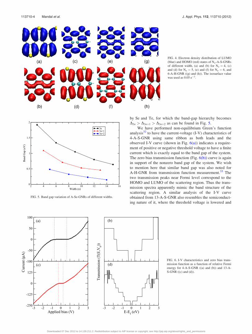
authors report 4-A-S-GNR as a metallic system. Fig. 3 dis-
plays the band-structures of 4-6-A-S-GNR, those are
obtained from our DFT calculations, clearly indicating a
band gap of 0.67 eV for 4-A-S-GNR. In general, GGA under-
estimates the band gaps for 2D carbon-base materials. In
addition, band gap is very sensitive to the size of the basis
function, threshold energy, and maximum force tolerance on
each atom. Thus, further experimental verification is
required for the present conflict.
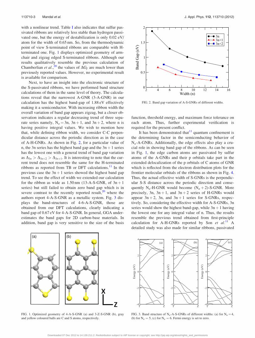
It has been demonstrated that11 quantum confinement is
the determining factor in the semiconducting behavior of
Na-A-GNRs. Additionally, the edge effects also play a cru-
cial role in showing band gap of the ribbons. As can be seen
in Fig. 1, the edge carbon atoms are passivated by sulfur
atoms of the A-GNRs and their p orbitals take part in the
extended delocalization of the p orbitals of C atoms of GNR
which is reflected from the electron distribution plots for the
frontier molecular orbitals of the ribbons as shown in Fig. 4.
Thus, the actual effective width of S-GNRs is the perpendic-
ular S-S distance across the periodic direction and conse-
quently Na-H-GNR would become (Naþ 2)-S-GNR. More
precisely, 3n, 3nþ 1, and 3nþ 2 series of H-GNRs would
appear 3nþ 2, 3n, and 3nþ 1 series for S-GNRs, respec-
tively. So, considering the effective width for A-S-GNRs, 3n
series would show the highest band-gap, while 3nþ 1 having
the lowest one for any integral value of n. Thus, the results
resemble the previous trend obtained from first-principle
calculation for A-H-GNRs reported by Son et al.11 A
detailed study was also made for similar ribbons, passivated
FIG. 1. Optimized geometry of 4-A-S-GNR (a) and 3-Z-S-GNR (b), gray
and yellow coloured balls are C and S atoms, respectively.
2 4 6 8 10 12 14 16Width (n)
0
0.5
1
1.5
2
Ban
d G
ap (e
V)
3n3n+13n+2
FIG. 2. Band gap variation of A-S-GNRs of different widths.
Γ Z-4
-2
0
2
4
Ener
gy (e
V)
Γ Z-4
-2
0
2
4
Ener
gy (e
V)
Γ Z-4
-2
0
2
4
Ener
gy (e
V)
(a) (b) (c)
FIG. 3. Band structure of Na-A-S-GNRs of different widths: (a) for Na ¼ 4,
(b) for Na ¼ 5, (c) for Na ¼ 6. Fermi energy is set to zero.
113710-3 Mandal et al. J. Appl. Phys. 112, 113710 (2012)
Downloaded 07 Dec 2012 to 14.139.211.2. Redistribution subject to AIP license or copyright; see http://jap.aip.org/about/rights_and_permissions
by Se and Te, for which the band-gap hierarchy becomes
D3n > D3nþ1 > D3nþ2 as can be found in Fig. 5.
We have performed non-equilibrium Green’s function
analysis32 to have the current-voltage (I-V) characteristics of
4-A-S-GNR using same ribbon as both leads and the
observed I-V curve (shown in Fig. 6(a)) indicates a require-
ment of positive or negative threshold voltage to have a finite
current which is exactly equal to the band gap of the system.
The zero bias transmission function (Fig. 6(b)) curve is again
in support of the nonzero band gap of the system. We wish
to mention here that similar band gap was also noted for
A-H-GNR from transmission function measurement.33 The
two transmission peaks near Fermi level correspond to the
HOMO and LUMO of the scattering region. Thus the trans-
mission spectra apparently mimic the band structure of the
scattering region. A similar analysis of the I-V curve
obtained from 13-A-S-GNR also resembles the semiconduct-
ing nature of it, where the threshold voltage is lowered and
FIG. 4. Electron density distribution of LUMO
(blue) and HOMO (red) states of Na-A-S-GNRs
of different width, (a) and (b) for Na ¼ 4, (c)
and (d) for Na ¼ 5, (e) and (f) for Na ¼ 6, and
6-A-H-GNR ((g) and (h)). The isosurface value
was used as 0.05 e�3.
2 4 6 8 10 12 14 16Width (n)
0
0.5
1
1.5
2
Ban
d G
ap (e
V)
3n3n+13n+2
FIG. 5. Band gap variation of A-Se-GNRs of different widths.
-100
-50
0
50
100
-3 -2 -1 0 1 2 3Applied bias (V)
-250
-125
0
125Cur
rent
(μΑ
)
-3 -2 -1 0 1 2 3E-Ef (eV)
Tran
smis
sion
(T(E
,Vb))
(a)
(c)
(b)
(d)FIG. 6. I-V characteristics and zero bias trans-
mission function as a function of relative Fermi
energy for 4-A-S-GNR ((a) and (b)) and 13-A-
S-GNR ((c) and (d)).
113710-4 Mandal et al. J. Appl. Phys. 112, 113710 (2012)
Downloaded 07 Dec 2012 to 14.139.211.2. Redistribution subject to AIP license or copyright; see http://jap.aip.org/about/rights_and_permissions
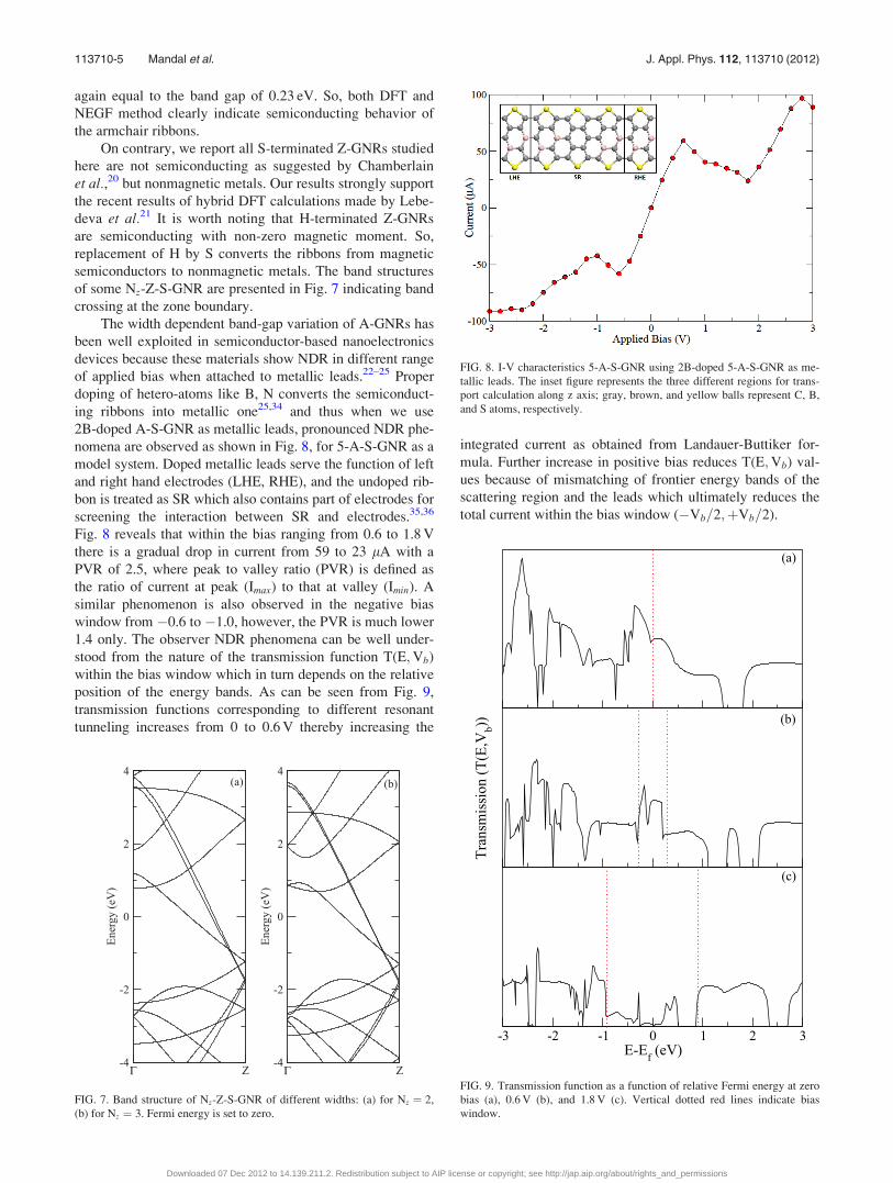
again equal to the band gap of 0.23 eV. So, both DFT and
NEGF method clearly indicate semiconducting behavior of
the armchair ribbons.
On contrary, we report all S-terminated Z-GNRs studied
here are not semiconducting as suggested by Chamberlain
et al.,20 but nonmagnetic metals. Our results strongly support
the recent results of hybrid DFT calculations made by Lebe-
deva et al.21 It is worth noting that H-terminated Z-GNRs
are semiconducting with non-zero magnetic moment. So,
replacement of H by S converts the ribbons from magnetic
semiconductors to nonmagnetic metals. The band structures
of some Nz-Z-S-GNR are presented in Fig. 7 indicating band
crossing at the zone boundary.
The width dependent band-gap variation of A-GNRs has
been well exploited in semiconductor-based nanoelectronics
devices because these materials show NDR in different range
of applied bias when attached to metallic leads.22–25 Proper
doping of hetero-atoms like B, N converts the semiconduct-
ing ribbons into metallic one25,34 and thus when we use
2B-doped A-S-GNR as metallic leads, pronounced NDR phe-
nomena are observed as shown in Fig. 8, for 5-A-S-GNR as a
model system. Doped metallic leads serve the function of left
and right hand electrodes (LHE, RHE), and the undoped rib-
bon is treated as SR which also contains part of electrodes for
screening the interaction between SR and electrodes.35,36
Fig. 8 reveals that within the bias ranging from 0.6 to 1.8 V
there is a gradual drop in current from 59 to 23 lA with a
PVR of 2.5, where peak to valley ratio (PVR) is defined as
the ratio of current at peak (Imax) to that at valley (Imin). A
similar phenomenon is also observed in the negative bias
window from �0.6 to �1.0, however, the PVR is much lower
1.4 only. The observer NDR phenomena can be well under-
stood from the nature of the transmission function T(E;Vb)
within the bias window which in turn depends on the relative
position of the energy bands. As can be seen from Fig. 9,
transmission functions corresponding to different resonant
tunneling increases from 0 to 0.6 V thereby increasing the
integrated current as obtained from Landauer-Buttiker for-
mula. Further increase in positive bias reduces T(E;Vb) val-
ues because of mismatching of frontier energy bands of the
scattering region and the leads which ultimately reduces the
total current within the bias window (�Vb=2;þVb=2).
Γ Z-4
-2
0
2
4
Ener
gy (e
V)
Γ Z-4
-2
0
2
4
Ener
gy (e
V)
(a) (b)
FIG. 7. Band structure of Nz-Z-S-GNR of different widths: (a) for Nz ¼ 2,
(b) for Nz ¼ 3. Fermi energy is set to zero.
FIG. 8. I-V characteristics 5-A-S-GNR using 2B-doped 5-A-S-GNR as me-
tallic leads. The inset figure represents the three different regions for trans-
port calculation along z axis; gray, brown, and yellow balls represent C, B,
and S atoms, respectively.
-3 -2 -1 0 1 2 3E-Ef (eV)
Tran
smis
sion
(T(E
,Vb))
(a)
(b)
(c)
FIG. 9. Transmission function as a function of relative Fermi energy at zero
bias (a), 0.6 V (b), and 1.8 V (c). Vertical dotted red lines indicate bias
window.
113710-5 Mandal et al. J. Appl. Phys. 112, 113710 (2012)
Downloaded 07 Dec 2012 to 14.139.211.2. Redistribution subject to AIP license or copyright; see http://jap.aip.org/about/rights_and_permissions
IV. CONCLUSIONS
In conclusion, newly synthesized S-GNRs are realizable
from the thermodynamic stand point as compared to
H-GNRs. All S-GNRs are thermodynamically more stable
than the bare ribbons and their stability depends on the edge
structure as well as ribbon width. Unlike hydrogen-
terminated graphene ribbons sulfur-terminated zigzag rib-
bons are more stable than armchair ribbons of similar width.
This is mainly because of the favored orientation of unhybri-
dised p orbitals of the terminal S atoms and greater S-S inter-
action in Z-S-GNRs. Band structure analysis of the ribbons
reveals that A-S-GNRs are semiconducting and their band
gap decreases with increasing ribbon width following the
sequence D3n > D3nþ2 > D3nþ1 which seems to be different
from that of A-H-GNRs. However, a deep insight reveals
that p-orbitals of terminal sulfur atoms take part into
extended delocalization of the ribbons thereby taking into
account the S atoms as part of ribbon width. Thus, the cor-
rected band-gap sequence, D3nþ1 > D3n > D3nþ2, resembles
the same for A-H-GNRs. So, the participation of S atoms in
the frontier orbitals is the crucial point for determining band
gap hierarchy. Similar things happen for Se and Te passi-
vated A-GNRs also, where D3nþ2 goes below D3nþ1 due to
more pronounced edge effect. The I-V characteristics
obtained from the NEGF analysis using semiconducting
leads demand a threshold voltage to have a finite current
which is again in support of the semiconducting nature of the
A-S-GNRs. On the other hand, while using doped metallic
ribbons as leads, there appears NDR in different bias regions.
Although GGA-PBE underestimates the band opening to
some extent, we do hope that our findings will motivate the
experimentalists for measuring the band-gap for A-S-GNR
so as to implement it in the future generation graphene-based
nanoelectronics and optical devices.
ACKNOWLEDGMENTS
The authors gratefully acknowledge the financial sup-
port from DST, New Delhi [SR/NM/NS-49/2007], through
research grants. The first three authors are thankful to CSIR,
Govt. of India for providing them research associateship/
fellowship.
1K. S. Novoselov, A. K. Geim, S. V. Morozov, D. Jiang, Y. Zhang, S. V.
Dubonos, I. V. Grigorieva, and A. A. Firsov, Science 306, 666 (2004).2M. Fujita, K. Wakabayashi, K. Nakada, and K. Kusakabe, J. Phys. Soc.
Jpn. 65, 1920 (1996).3K. Nakada, M. Fujita, G. Dresselhaus, and M. S. Dresselhaus, Phys. Rev. B
54, 17954 (1996).
4K. Wakabayashi, Phys. Rev. B 64, 125428 (2001).5K. Sasaki, S. Saito, and R. Saito, Appl. Phys. Lett. 88, 113110 (2006).6D. Gunlycke, J. Li, J. W. Mintmire, and C. T. White, Appl. Phys. Lett. 91,
112108 (2007).7L. Yang, C.-H. Park, Y.-W. Son, M. L. Cohen, and S. G. Louie, Phys.
Rev. Lett. 99, 186801 (2007).8O. Hod, V. Barone, J. E. Peralta, and G. E. Scuseria, Nano Lett. 7, 2295
(2007).9Y. H. Lu, R. Q. Wu, L. Shen, M. Yang, Z. D. Sha, Y. Q. Cai, P. M. He,
and Y. P. Feng, Appl. Phys. Lett. 94, 122111 (2009).10Y.-W. Son, M. L. Cohen, and S. G. Louie, Nature 444, 347 (2006); 446,
342 (2007).11Y.-W. Son, M. L. Cohen, and S. G. Louie, Phys. Rev. Lett. 97, 216803
(2006); 98, 089901 (2007).12M. Y. Han, B. Ozyilmaz, Y. B. Zhang, and P. Kim, Phys. Rev. Lett. 98,
206805 (2007).13V. Barone, O. Hod, and G. E. Scuseria, Nano Lett. 6, 2748 (2006).14E. Rudberg, P. Salek, and Y. Luo, Nano Lett. 7, 2211 (2007).15Y. Kobayashi, K. I. Fukui, T. Enoki, K. Kusakabe, and Y. Kaburagi, Phys.
Rev. B 71, 193406 (2005).16Z. F. Wang, Q. X. Li, H. Zheng, H. Ren, H. B. Su, and Q. W. Shi, Phys.
Rev. B 75, 113406 (2007).17X. Li, X. Wang, L. Zhang, S. Lee, and H. Dai, Science 319, 1229
(2008).18M. Ezawa, Phys. Rev. B 73, 045432 (2006).19A. Chuvilin, E. Bichoutskaia, M. C. Gimenez-Lopez, T. W. Chamberlain,
G. A. Rance, N. Kuganathan, J. Biskupek, U. Kaiser, and A. N. Khlobys-
tov, Nature Mater. 10, 687 (2011).20T. W. Chamberlain, J. Biskupek, G. A. Rance, A. Chuvilin, T. J.
Alexander, E. Bichoutskaia, U. Kaiser, and A. N. Khlobystov, ACS Nano
6, 3943 (2012).21I. V. Lebedeva, A. M. Popov, A. A. Knizhnik, A. N. Khlobystov, and B.
V. Potapkin, Nanoscale 4, 4522 (2012).22H. Ren, Q.-X. Li, Y. Luo, and J. Yang, Appl. Phys. Lett. 94, 173110
(2009).23W. Y. Kim, Y. C. Choi, S. K. Min, Y. Cho, and K. S. Kim, Chem. Soc.
Rev. 38, 2319 (2009).24W. Y. Kim, S. K. Kwon, and K. S. Kim, Phys. Rev. B 76, 033415
(2007).25A. Pramanik, S. Sarkar, and P. Sarkar, J. Phys. Chem. C 116, 18064
(2012).26S. W. Lee, A. Kornblit, D. Lopez, S. V. Rotkin, A. A. Sirenko, and H.
Grebel, Nano Lett. 9, 1369 (2009).27Y. Hikita, L. F. Kourkoutis, T. Susaki, D. A. Muller, H. Takagi, and H. Y.
Hwang, Phys. Rev. B 77, 205330 (2008).28N. Troullier and J. L. Martins, Phys. Rev. B 43, 1993 (1991).29J. M. Soler, E. Artacho, J. D. Gale, A. Garcia, J. Junquera, P. Ordejon, and
D. Sanchez-Portal, J. Phys.: Condens. Matter 14, 2745 (2002).30J. P. Perdew, K. Burke, and M. Ernzerhof, Phys. Rev. Lett. 77, 3865
(1996).31M. Brandbyge, J.-L. Mozos, P. Ordejon, J. Taylor, and K. Stokbro, Phys.
Rev. B 65, 165401 (2002).32S. Datta, Electronic Transport in Mesoscopic Systems, edited by H.
Ahmed, M. Pepper, and A. Broers (Cambridge University Press, Cam-
bridge, England, 1995).33M. Topsakal, V. M. K. Bagci, and S. Ciraci, Phys. Rev. B 81, 205437
(2010).34H. S. Kang and A. Pramanik, J. Chem. Phys. 135, 124708 (2011).35L. Wirtz, A. Martin, and A. Rudio, Phys. Rev. Lett. 96, 126104 (2006).36L. Yang, J. Deslippe, C.-H. Park, M. L. Cohen, and S. G. Louie, Phys.
Rev. Lett. 103, 186802 (2009).
113710-6 Mandal et al. J. Appl. Phys. 112, 113710 (2012)
Downloaded 07 Dec 2012 to 14.139.211.2. Redistribution subject to AIP license or copyright; see http://jap.aip.org/about/rights_and_permissions