EECS 40 Fall 2002 Lecture 4 W. G. Oldham and S. Ross
Lecture 4• Last time
– Gate delay: why it happens (Capacitance! Resistance!)– Voltage rise and fall through logic circuits is gradual – (delay between input and output at 50% of final value) found graphically– Used clock signal to prevent false output (due to signals delayed different
amounts)
• Now we will– Get to calculating delays for circuits (RC analysis)– Review fundamental knowledge of electric circuits

EECS 40 Fall 2002 Lecture 4 W. G. Oldham and S. Ross
REVIEW OF ELECTRICAL QUANTITIES AND BASIC CIRCUIT ELEMENTS
• Solids in which outer-most atomic electrons are free to move around are called metals.– Metals typically have ~ 1 “free electron” per atom (~ 5 X10²²/cm3)– Charge on a free electron is ”e” or “q”, where |e| = 1.6 x 10⁻¹⁹ C
Free ChargeMost matter is macroscopically electrically neutral most of the time. Exceptions: clouds in thunderstorm, people on carpets in dry weather, plates of a charged capacitor, etc.
Microscopically, of course, matter is full of charges. Consider solids:
Al or Cu – good metallic conductor – great for wires
Quartz – good insulator – great for dielectric
Si or GaAs – classic semiconductors
• Solids in which all charges are bound to atoms are called insulators.
• Semiconductors are insulators in which electrons are not tightly bound and thus can be easily “promoted” to a free state (by heat or even by “doping” with a foreign atom).

EECS 40 Fall 2002 Lecture 4 W. G. Oldham and S. Ross
CHARGE (cont.)Charge flow Current Charge storage Energy
Definition of current i (or I)
Note: Current has sign
S
C
dt
dq (A) i
second per coulomb 1 offlow Amperes)(in i
where q is the charge in coulomb and t is the time in sec
Examples:
(a)
right) to (leftA 165106.1910
19106.1510i
nanosecondevery direction) this (call right toflow
19106.1 value of charges unit positive 510
A
Ce
right) to (leftmA 6.13106.1610
16106.11010-i
dmicroseconevery wirea in right toflow electrons 1010
(b)

EECS 40 Fall 2002 Lecture 4 W. G. Oldham and S. Ross
CURRENT & CURRENT DENSITY
Define Current Density by Example:
Semiconductor with free electrons
2 c m
10 cm
1 cmC2
C1
X
Wire attached to ends
sec 1025.6
/106.1
sec/1 1819
electrons
electronC
C
•Electron flow (in negative X direction) consists of
Suppose we force a + 1A current from C1 to C2. Then
•Current of 1A flows in the semiconductor (in +X direction)
•Current Density = Current / (Cross-Sectional area current goes thru)
•Current density of above = 1 A / (2 cm • 1 cm) = 0.5 A/cm2

EECS 40 Fall 2002 Lecture 4 W. G. Oldham and S. Ross
CURRENT & CURRENT DENSITY (cont.)
Note: Typical dimensions of integrated circuit components are in the range of . What is the current density in a component with [1m]² area carrying 5A?
)cm410(m1
• A wire carrying 1 amp has a cross-section, then the current density is
2cm 2102 1 mm
2 100
2101
cmA
2A/cm 5002cm)410(1
A6105
Answer

EECS 40 Fall 2002 Lecture 4 W. G. Oldham and S. Ross
POSSIBLE CONCEPTUAL ISSUES
1 How does charge move through the wire?
Remember a wire has a huge number of free carriers moving very fast but randomly (because of thermal energy)
Drift concept: Now add even a modest electric field
Carriers “feel” an electric field along the wire and tend to drift with it (+ sign charge) or against it ( charge carrier). This drift is still small compared to the random motion.
2 Sign of the charge carriers: It is often negative (for metals); in silicon, it can be either negative or positive…we don’t care for circuit analysis.

EECS 40 Fall 2002 Lecture 4 W. G. Oldham and S. Ross
POSSIBLE CONCEPTUAL ISSUES (con’t)
4. Field or Current can have positive or negative sign.
Examples: I = 0.2 mA same as I = 0.2 mA going left to right going right to left
3. Electric field is in the direction positive charge carriers move. Thus if we have an electrical field in the Z direction, positive charges (ions, positrons, whatever) will experience a force in the positive Z direction. Negatively charged particles will experience the force in the –Z direction.
Thus the free carriers we will be concerned with (electrons with negative charge and “holes” with positive charge) will move against and with the electric field respectively.

EECS 40 Fall 2002 Lecture 4 W. G. Oldham and S. Ross
POSSIBLE CONCEPTUAL ISSUES (con’t)
5. When we have unknown quantities such as current or voltage, we of course do not know the sign. A question like “Find the current in the wire” is always accompanied by a definition of the direction:
6. To solve circuits, you may need to specify reference directions for currents. But there is no need to guess the reference direction so that the answer comes out positive….Your guess won’t affect what the charge carriers are doing! Of course you will find that your intuition and experience will often guide you to define a current direction so that the answer comes out positive.
In this example if the current turned out to be 1mA, but flowing to the left we would merely say I = -1mA.
(or)I I
EECS 40 Fall 2002 Lecture 4 W. G. Oldham and S. Ross
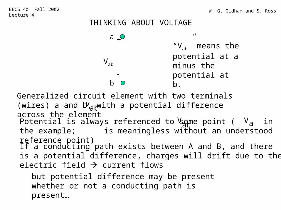
THINKING ABOUT VOLTAGE
but potential difference may be present whether or not a conducting path is present…
Generalized circuit element with two terminals (wires) a and b, with a potential difference across the elementab
v
a
b
Vab
“Vab” means the potential at a minus the potential at b.
If a conducting path exists between A and B, and there is a potential difference, charges will drift due to the electric field current flows
abV aVPotential is always referenced to some point ( in the example; is
meaningless without an understood reference point)

EECS 40 Fall 2002 Lecture 4 W. G. Oldham and S. Ross
Suppose you have an unlabelled battery and you measure its voltage with a digital voltmeter. It will tell you magnitude and sign of the voltage.
SIGN CONVENTIONS
With this circuit, you are measuring
(or ). DVM indicates 1.4, so by 1.4 V. Which is the positive battery terminal? 1.401
DVM
a
b
bVaV
abV
bVaV
Answer: terminal b )aVbV(
DVM
b
a
Now you make a change. What would this circuit measure?
Answer: +1.401VNote that we have used “ground” symbol ( ) for reference node on DVM. Often it is labeled “C” or “common.”

EECS 40 Fall 2002 Lecture 4 W. G. Oldham and S. Ross
SIGN CONVENTIONS (cont.)
How is VAD related to VAB, VBC etc ?
Lets put a bunch of batteries, say 1.5V and 9V in series to see what we already know about sign conventions:
Example 1
+ ++ 1.5V1.5V 9VA B C D
VAB = -1.5, VBC = -1.5, and VAC = -3 so clearly VAC =VAB+VBC etc.
What is VAD ? Answer: Clearly A is above D by 9V – 3V or 6V. That is consistent with VAB+VBC + VCD= -1.5 –1.5 + 9 = 6V
Example 2 How are single-subscript voltages related to double-subscript voltages?
+ ++ 1.5V1.5V 9VA B C D
V1
VX
+
+
-
-
Answer: Clearly V1 = 1.5 = - VAB = VBA
VX = -6 = VDA

EECS 40 Fall 2002 Lecture 4 W. G. Oldham and S. Ross
SIGN CONVENTIONS (cont.)
Solve for
Just as in the physical world, we do not know a priori the sign (or magnitude) of voltages or currents; we don’t know them in the theoretical world until solving for them, so we just define voltages and currents and accept that half of the time they will be negative (quite analogously to probing with a DC meter).
Example 1 xi
Remembering Ohm’s law,
Here
mA1105.1
V5.1i
3x
mA1ix
Note that in this case, the current flows counterclockwise, i.e., opposite to arrow defining
Here
xi
mA1ix
+
1.5K1.5
+Batt
Vx
ix
Example 2 Solve for ix
+
ix
1.5K1.5
+
Vx
Batt

EECS 40 Fall 2002 Lecture 4 W. G. Oldham and S. Ross
KEEPING THE VOLTAGE SIGNS STRAIGHT
Labeling Conventions• Indicate + and terminals clearly; or label terminals with letters• The + sign corresponds to the first subscript; the sign to the second
subscript. Therefore, Vab = - Vba
Note: The labeling convention has nothing to do with whether or not v > 0 or v < 0
+
vcd
+ vbd
d
+
1 V
a
b
V +c Using sign conventions:
1V12V
thus,2V ; 1V
cb
caab
Obviously Vcd +Vdb = Vcb too. Then if Vbd = 5V, what is Vcd?
Answer: Vcd -5 = -1 so Vcd = 4V

EECS 40 Fall 2002 Lecture 4 W. G. Oldham and S. Ross
POWER IN ELECTRIC CIRCUITS
Power: Transfer of energy per unit time (Joules per second = Watts)
Concept: in falling through a positive potential drop V, a positive charge q gains energy• potential energy change = qV for each charge q• Rate is given by # charges/sec
Power = P = V (dq/dt) = VI
P = V I Volt Amps = Volts Coulombs/sec = Joules/sec = Watts
Circuit elements can absorb or release power (i.e., from or to the rest of the circuit); power can be a function of time.
How to keep the signs straight for absorbing and releasing power?
+ Power absorbed into element
Power delivered from element

EECS 40 Fall 2002 Lecture 4 W. G. Oldham and S. Ross
“ASSOCIATED REFERENCE DIRECTIONS”
It is often convenient to define the current through a circuit element as positive when entering the terminal associated with the + reference for voltage
For positive current and positive voltage, positive charge “falls down” a potential “drop” in moving through the circuit element: it absorbs power
• P = VI > 0 corresponds to the element absorbing power if the definitions of I and V are associated.How can a circuit element absorb power?
By converting electrical energy into heat (resistors in toasters); light (light bulbs); acoustic energy (speakers); by storing energy (charging a battery).
Negative power releasing power to rest of circuit
VThis box representsthe re st of the c ircui t
i
Circuit element
+
-
Here, I and V are “associated”
EECS 40 Fall 2002 Lecture 4 W. G. Oldham and S. Ross
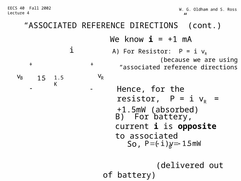
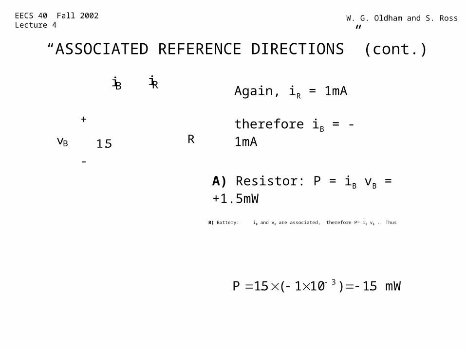
A) For Resistor: P = i vR (because we are using “associated reference directions”)
“ASSOCIATED REFERENCE DIRECTIONS” (cont.)
1.5
+
+
vRvB
i
Hence, for the resistor, P = i vR
= +1.5mW (absorbed)
1.5K
B) For battery, current i is opposite to associated
mW 5.1i)v(P B So,
(delivered out of battery)
We know i = +1 mA
EECS 40 Fall 2002 Lecture 4 W. G. Oldham and S. Ross
“ASSOCIATED REFERENCE DIRECTIONS” (cont.)
B) Battery: iB and vB are associated, therefore P= iB vB . Thus
1.5
+
RvB
iRiBAgain, iR = 1mA
therefore iB = -1mA
mW5.1)101(5.1P 3
A) Resistor: P = iB vB = +1.5mW

EECS 40 Fall 2002 Lecture 4 W. G. Oldham and S. Ross
EXAMPLES OF CALCULATING POWER
Find the power absorbed by each element
Element :
Element : mW 6mA) 2V(3
Element : mW 0.5mA) 1V(0.5
mW 9mA) 33V(
Element : mW 2.5mA) 1V(2.5
+
+
V
1 V
+a
b
c
V
+
1 V2.5 mA
0.5 mA
3 mA
3V
3 mA
flip current direction:

EECS 40 Fall 2002 Lecture 4 W. G. Oldham and S. Ross
BASIC CIRCUIT ELEMENTS
• Voltage Source• Current Source
• Resistor• Capacitor
• Inductor
(like ideal battery)(always supplies some constant given current)(Ohm’s law)(capacitor law – based on energy storage in electric field of a dielectric)
(inductor law – based on energy storage in magnetic field produced by a current)

EECS 40 Fall 2002 Lecture 4 W. G. Oldham and S. Ross
DEFINITION OF IDEAL VOLTAGE SOURCE
Special cases:
upper case V constant voltage … called “DC”
lower case v general voltage, may vary with time
Symbol
V
Note: Reference direction for voltage source is unassociated (by convention)
Examples:
1) V = 3V
2) v = v(t) = 160 cos 377t
Current through voltage source can take on any value (positive or negative) but not infinite
EECS 40 Fall 2002 Lecture 4 W. G. Oldham and S. Ross
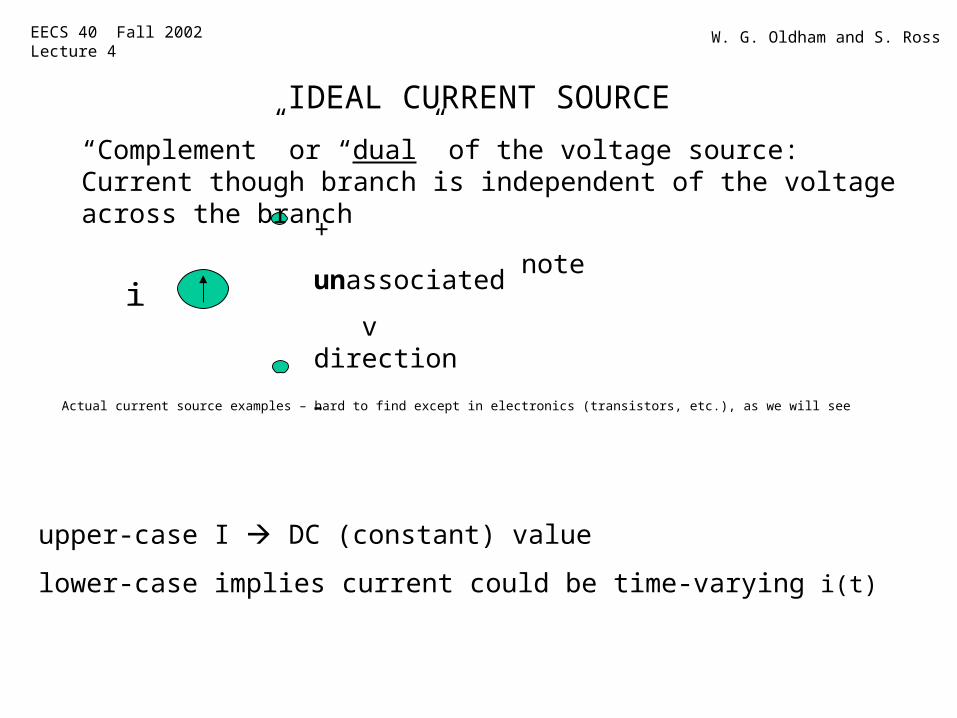
IDEAL CURRENT SOURCE
Actual current source examples – hard to find except in electronics (transistors, etc.), as we will see
i
+ note unassociated
v direction
upper-case I DC (constant) value
lower-case implies current could be time-varying i(t)
“Complement” or “dual” of the voltage source: Current though branch is independent of the voltage across the branch

EECS 40 Fall 2002 Lecture 4 W. G. Oldham and S. Ross
CURRENT-VOLTAGE CHARACTERISTICS OF VOLTAGE & CURRENT SOURCES
Describe a two-terminal circuit element by plotting current vs. voltage
V
i
Assume unassociated signs
Ideal voltage source
V
If V is positive and I is only positive
releasing power
absorbing power (charging)
But this is arbitrary; i might be negative so we extend into 2nd quadrant
But this is still arbitrary, V could be negative; all four quadrants are possible
absorbing power
releasing power

EECS 40 Fall 2002 Lecture 4 W. G. Oldham and S. Ross
CURRENT-VOLTAGE CHARACTERISTICS OF VOLTAGE & CURRENT SOURCES (con’t)
V
iabsorbing power releasing power
Remember the voltage across the current source can be any finite value (not just zero)
Ideal current source
i
+
v
If i is positive then we are confined to quadrants 4 and 1:
And do not forget i can be positive or negative. Thus we can be in any quadrant.

EECS 40 Fall 2002 Lecture 4 W. G. Oldham and S. Ross
RESISTOR
If we use associated current and voltage (i.e., i is defined as into + terminal), then v = iR (Ohm’s law)
+
v
i
R
Question: What is the I-V characteristic for a 1K resistor? Draw on axis below. I (mA)
V1 2 3
1
2
3
Slope = 1/R
Answer: V = 0 I = 0
V = 1V I = 1 mA V = 2V I = 2 mA
etc
Note that all wires and circuit connections have resistance, though we will most often approximate it to be zero. But we can (and do) deliberately construct circuit elements with some desired resistance, even very large values such as 10M.
EECS 40 Fall 2002 Lecture 4 W. G. Oldham and S. Ross
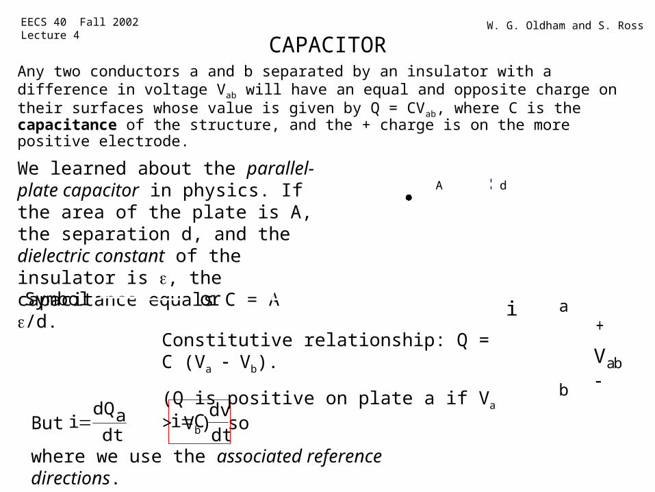
CAPACITORAny two conductors a and b separated by an insulator with a difference in voltage Vab will have an equal and opposite charge on their surfaces whose value is given by Q = CVab, where C is the capacitance of the structure, and the + charge is on the more positive electrode.
We learned about the parallel-plate capacitor in physics. If the area of the plate is A, the separation d, and the dielectric constant of the insulator is , the capacitance equals C = A /d.
A d
Symbol or
But so
where we use the associated reference directions.dt
adQi
dtdv
Ci
i
+a
b
VabConstitutive relationship: Q = C (Va Vb).
(Q is positive on plate a if Va > Vb)

EECS 40 Fall 2002 Lecture 4 W. G. Oldham and S. Ross
ENERGY STORED IN A CAPACITOR
You might think the energy (in Joules) is QV, which has the dimension of joules. But during charging the average voltage was only half the final value of V.
Thus, energy is .22
1
2
1CVQV

EECS 40 Fall 2002 Lecture 4 W. G. Oldham and S. Ross
ENERGY STORED IN A CAPACITOR (cont.)
More rigorous derivation: During charging, the power flow is v i into the capacitor, where i is into + terminal. We integrate the power from t = 0 (v = 0) to t = end (v = V). The integrated power is the energy
i
v
+
Vv
0vdq vdt
endt
0
dtdqend
0vdt ivE
but dq = C dv. (We are using small q instead of Q to remind us that it is time varying . Most texts use Q.)
2CV21Vv
0vdv CvE

EECS 40 Fall 2002 Lecture 4 W. G. Oldham and S. Ross
Capacitor Inductor
dt
dVCi
dt
diLv
2CV2
1E 2LI
2
1E
INDUCTORS
Inductors are the dual of capacitors – they store energy in magnetic fields that are proportional to current.
Switching properties: Just as capacitors demand v be continuous (no jumps in V), inductors demand i be continuous (no jumps in i ). Reason? In both cases the continuity follows from non-infinite, i.e., finite, power flow.
Capacitor Inductor v is continuous i is continuous i can jump V can jump Do not short circuit a charged capacitor (produces current)
Do not open an inductor with current flowing (produces voltage)