1
Design for ESD Prevention & ESD Failure Analysis Techniques Cheryl Tulkoff
CTEA Electronics Design & Manufacturing Expo
February 21, 2012
© 2004 - 2007 © 2004 - 2010
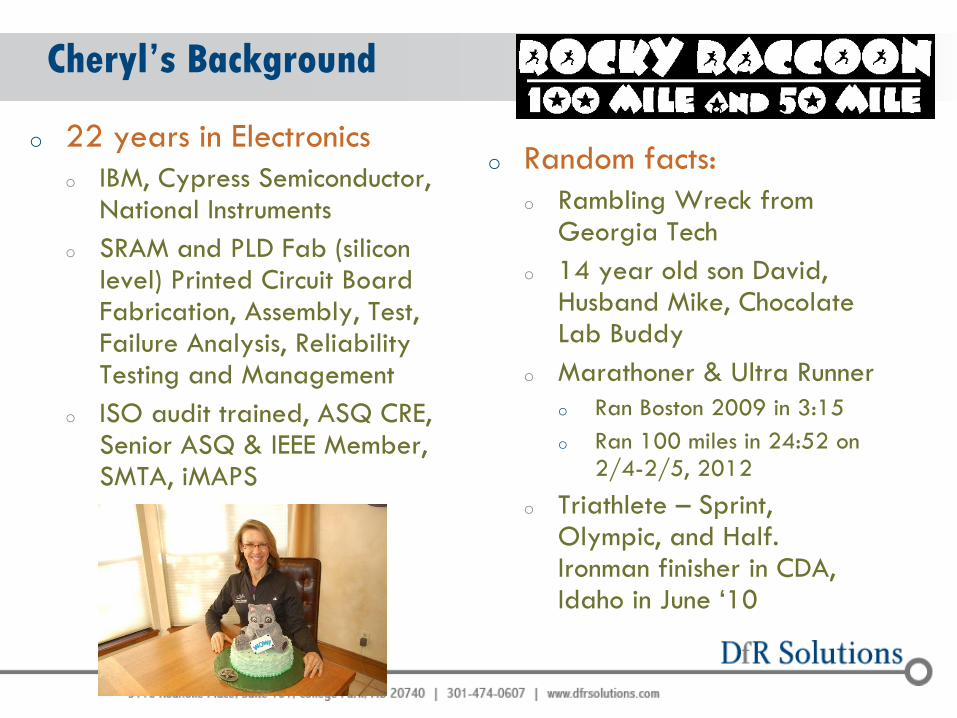
Cheryl’s Background
o 22 years in Electronics
o IBM, Cypress Semiconductor, National Instruments
o SRAM and PLD Fab (silicon level) Printed Circuit Board Fabrication, Assembly, Test, Failure Analysis, Reliability Testing and Management
o ISO audit trained, ASQ CRE, Senior ASQ & IEEE Member, SMTA, iMAPS
o Random facts:
o Rambling Wreck from Georgia Tech
o 14 year old son David, Husband Mike, Chocolate Lab Buddy
o Marathoner & Ultra Runner
o Ran Boston 2009 in 3:15
o Ran 100 miles in 24:52 on 2/4-2/5, 2012
o Triathlete – Sprint, Olympic, and Half. Ironman finisher in CDA, Idaho in June ‘10
3
o ESD Protection is necessary at the IC, component package
and system level
o Different approaches are needed to achieve reliable
protection
o Designing for ESD impacts both the product design and
the manufacturing process controls
o What technologies are available to assure a reliable ESD
protected product?
o At the IC level
o At the component package level
o At the system level
Design for ESD Prevention: What Do You Need to Do?
4 4
Good General Design Practices for ESD Prevention
o Know the ESD rating for each part, and select parts (where possible) for the best ESD rating
o Identify all ESD Sensitive Parts on drawings
o Mark Locations of ESD Sensitive parts on the Board with the ESD symbol
o Consider the entire System (Design) as ESD Sensitive o Use ESD Protection on all susceptible parts (not just System I/Os)
o Box or System I/O
o ESD Rating < Class 2 IEC 1000-4-2 (4000V) MANDATORY
o Internal Components (not exposed to outside connectors)
o ANSI/ESDA/JEDEC JS-001-2011, Human Body Model (HBM) - Component Level
o ESD Rating <= Class 1 MANDATORY
o ESD Rating < Class 2 WHEREVER POSSIBLE
5 5
ESD Design Practices (cont.)
o High Speed, RF and GaAs parts will be particularly sensitive to ESD
o GaAs Parts are typically rated as Class 0 (<250V) or Class 1A (<500V) – ONLY THE BEST PROTECTION DESIGN AND HANDLING PROCEDURES WILL PREVENT DAMAGE TO THESE PARTS!
o Reference: ANSI/ESDA/JEDEC JS-001-2011-:Human Body Model (HBM) - Component Level
o Place ESD sensitive components and traces to avoid locations where the board may be handled
o Consider ESD as well as RF shielding
o Where possible install protective devices before ESD sensitive parts
o Avoid Coupled ESD events – Do not route traces to ESD sensitive parts near lines connected to the outside world
6 6
ESD Design Practices (cont.)
o Perform Circuit analysis to insure effectiveness of ESD protection (Class 2 ANSI/ESDA/JEDEC JS-001-2011 for internal, IEC 1000-4-2 level 2 for I/O)
o Test Boards and Systems for Internal and I/O ESD tolerance
o ESD Protection devices must be connected to a good ground to accommodate up to 30A ESD spikes.
o If upset of operating circuits is to be avoided, a separate Earth ground should be used
7 7
ESD Sensitive Parts (Pin Sensitivity)
o Any pin of a discrete ESD sensitive part (FET, Transistor, etc) may need protection (if not connected to a supply)
o Input pins
o Can be sensitive since they have little or no built-in ESD protection
o Especially on high speed devices like GaAs ICs or discretes,
o Pins other than inputs (on an ESD sensitive part)
o Can also be sensitive because an ESD pulse can affect internal voltage levels
o Any improperly terminated or unprotected pin can be a conduit for ESD
o Supply pins
o Provide reference bias connections
o Should not need additional protection (as long as they are connected to the power supply)
o Outputs of logical or functional parts designed with active (usually buffered) output stages
o May have clamping diode protection to the supplies and may not need additional protection – check the part ESD rating
8 8
Evaluate Potential ESD
o If ESD sensitive parts are used in design, the circuitry connected to
device pins should be evaluated
o Insure that it provides “attenuation” to prevent voltage in excess of the
parts ESD rating from developing in case the pin or connected traces are
contacted during board handling or system assembly.
o Often the recommended circuit components for operation of the part
will provide adequate ESD protection.
o This should be verified by analysis or simulation and extra protection
added as required to limit the voltage seen at the part.
o Assumptions for analysis/simulation
o 2000V,1.5K, 100pf for Internal circuits
o 4000V, 330 Ohms, 150pf for I/Os
9
o What should you be concerned about?
o Completely different specification methods for ESD protection of components are commonly used
o Designers may need to gather comparable data points from differing graphs and tables.
o Some differentiators to look for and investigate further are outlined below
o IEC Rating: Verify that the ESD protection device is guaranteed to meet or exceed specifications in IEC 61000-4-2.
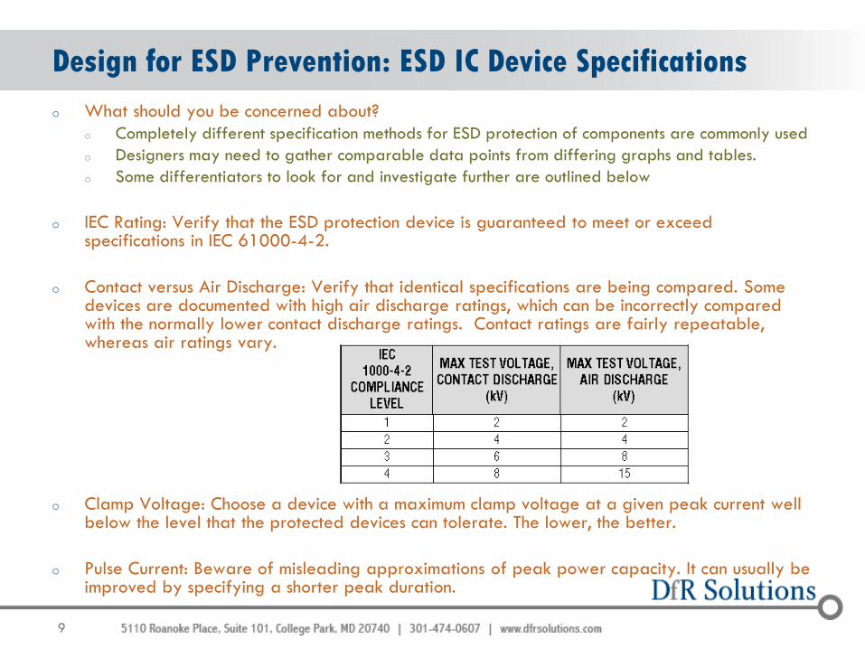
o Contact versus Air Discharge: Verify that identical specifications are being compared. Some devices are documented with high air discharge ratings, which can be incorrectly compared with the normally lower contact discharge ratings. Contact ratings are fairly repeatable, whereas air ratings vary.
o Clamp Voltage: Choose a device with a maximum clamp voltage at a given peak current well below the level that the protected devices can tolerate. The lower, the better.
o Pulse Current: Beware of misleading approximations of peak power capacity. It can usually be improved by specifying a shorter peak duration.
Design for ESD Prevention: ESD IC Device Specifications
10
o Response Time: Faster-acting devices reduce the width of the pulse transferred, and these devices can help attenuate the peak clamp voltage.
o Parasitic Capacitance: Added capacitance degrades I/O signal rise and fall times. On lower-speed signals, this stray capacitance can be lumped into or can displace the need for EMI capacitors.
o Parasitic Inductance: Higher impedance in the clamp path (to VDD or ground) can increase the effective system clamp voltage.
o Multistrike Capability: Verify that the protection designed-in can survive the expected life of the system. Resultant field failures are difficult to diagnose and can manifest themselves in unexpected functional errors, or even data loss.
o Integration and Matching: High-speed differential signals, such as in IEEE 1394, benefit from matched loading on the positive and negative lines of each pair. ESD protection products with multiple devices per package (such as thin-film silicon) can have intrachip device-to-device parasitic impedance matching of less than 0.1%. Unitary packages, however, may vary as much as 30% interchip matching. Printed-circuit-board (PCB) signal routing restrictions may also indicate a need for tight multidevice integration.
ESD IC Device Specifications
11
o Many ESD design rules
o Two common types of design rule verification/compliance
o Design Rule Checking (DRC): standard DRC tools with ESD marking layers
o Example: Mentor Graphics Calibre PERC
o Rule 1: Primary Protection for I/O Pad
o For each net in design, IF net is connected to IO Pad THEN check for up HBM diode and down HBM diode IF diode(s) missing THEN ESD Error
o Rule 2: Secondary Protection for I/O Pad
o For each net in design, IF net is connected to input buffer and IO Pad THEN check for CDM up diode and CDM down diode check if CDM resistor exists and is correct value IF diode(s) missing or resistor incorrect THEN ESD Error
o Net-oriented: in-house tools for circuit analysis.
Design for ESD Prevention & IC Design Rule Checking
12 12
ESD Protective Device Options
o Passive Networks
o Capacitors – Simple, Low cost
o Band-pass filters – Somewhat more complex, good ESD protection
o For lower speed devices
o Schottky Diodes – Simple, but capacitance loads HF circuits
o Diode Clamping Arrays – Good for LF circuits and outputs
o For higher speed devices (requiring low capacitance)
o Low capacity protection diodes (<1 pf) – Robust, Good HF compromise
o Polymer ESD (PESD) Protection devices (<0.25 pf)
o Excellent HF characteristics, small size 0402, 0603
o PESDs have limited Pulse life, good parts withstand 100 to 1000 strikes
o Operating voltage typically 5V, available to 12V, Trigger Voltage 100, 150V
13 13
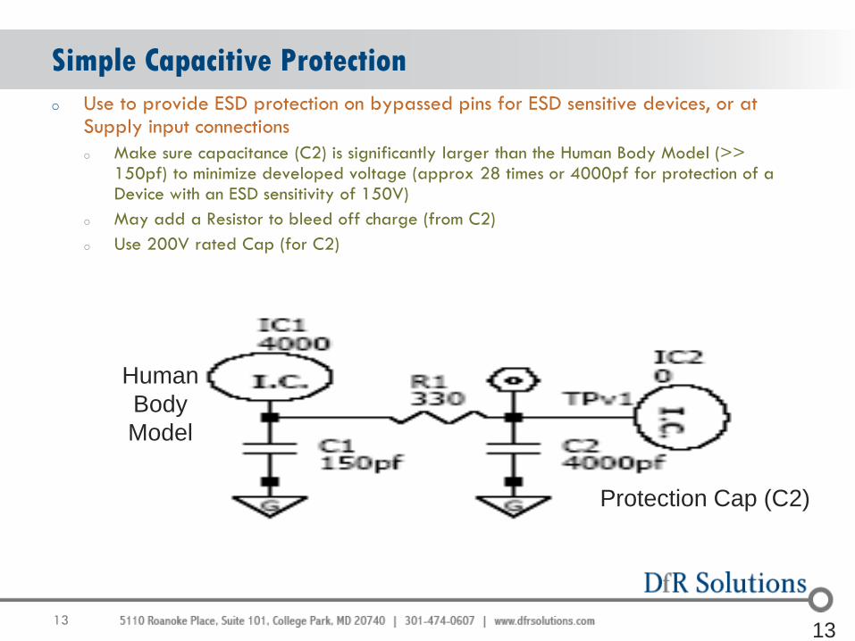
Simple Capacitive Protection
o Use to provide ESD protection on bypassed pins for ESD sensitive devices, or at Supply input connections
o Make sure capacitance (C2) is significantly larger than the Human Body Model (>> 150pf) to minimize developed voltage (approx 28 times or 4000pf for protection of a Device with an ESD sensitivity of 150V)
o May add a Resistor to bleed off charge (from C2)
o Use 200V rated Cap (for C2)
Human
Body
Model
Protection Cap (C2)
14 14
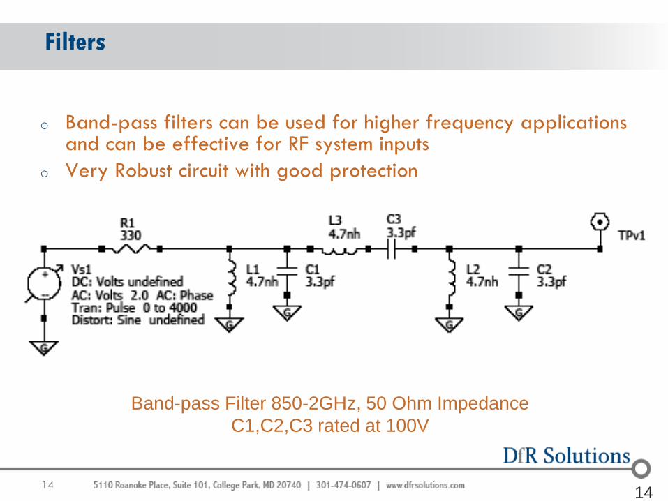
Filters
o Band-pass filters can be used for higher frequency applications and can be effective for RF system inputs
o Very Robust circuit with good protection
Band-pass Filter 850-2GHz, 50 Ohm Impedance
C1,C2,C3 rated at 100V
15 15
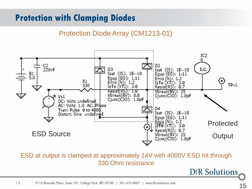
Protection with Clamping Diodes
Protection Diode Array (CM1213-01)
Protected
Output ESD Source
ESD at output is clamped at approximately 14V with 4000V ESD hit through
330 Ohm resistance
16
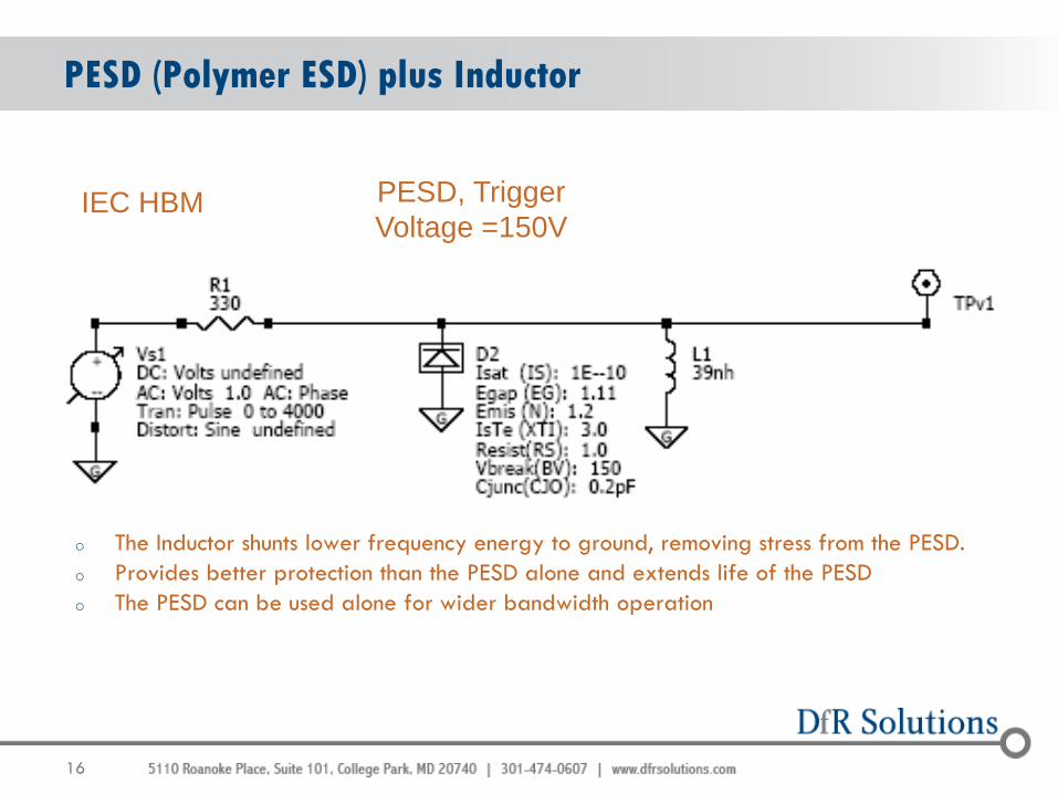
PESD (Polymer ESD) plus Inductor
o The Inductor shunts lower frequency energy to ground, removing stress from the PESD.
o Provides better protection than the PESD alone and extends life of the PESD
o The PESD can be used alone for wider bandwidth operation
P
E
S
D
PESD, Trigger
Voltage =150V IEC HBM
17 17
Summary of ESD Design Guidelines
o Design ESD Protection for External (System) I/Os to IEC HBM
Class 2 (4000V, 150pf, 330 Ohm) Including:
o RF or signal inputs
o Control and System I/Os that DO NOT have built in protection to
the required limit
o Design ESD Protection for Internal ESD sensitive parts to meet
ANSI/ESD S20.20
o Know the ESD rating of every part used
o Select parts (where possible) to meet ANSI/ESDA/JEDEC JS-
001-2011-:Human Body Model (HBM) - Component Level 2
o Parts rated less than Class 2 should have additional protection
circuitry added to protect the board during handling
18 18
ESD Design Guidelines (cont.)
o For External (System) Inputs use Robust protection:
o Band pass filter
o PESD plus Inductor (for Severe condition use PESD + Filter)
o For Internal ESD Sensitive pins use:
o Single bypass Cap (where possible)
o Filter if needed
o PESD or PESD plus Inductor
o Any Pin of an ESD sensitive part may be at Risk If It is NOT:
o Connected to a supply plane
o Adequately decoupled to GND (~4000pf @200V)
o Protected by a “filter” network (simulate for an ESD hit)
o External (System) Output or I/O
o Use low capacitance Clamping diodes (1pf)
o PESD if required for speed (.25pf)
19
ESD Failure Mechanisms,
Analysis and Tools
20
General Words of Wisdom on FA
o Before spending time and money on Failure Analysis, consider the following: o Consider FA “order” carefully. Some actions you take will limit or
eliminate the ability to perform follow on tests.
o Understand the limitations and output of the tests you select.
o Use partner labs who can help you select and interpret tests for capabilities you don’t have. Be careful of requesting a specific test. Describe the problem and define the data and output you need first.
o Pursue multiple courses of action. There is rarely one test or one root cause that will solve your problem.
o Don’t put other activities on hold while waiting for FA results. Understand how long it will take to get results
o Consider how you will use the data. How will it help you? o Information?
o Change course, process, supplier?
o Don’t pursue FA data if it won’t help you or you have no control over the path it might take you down. Some FA is just not worth doing
21 21
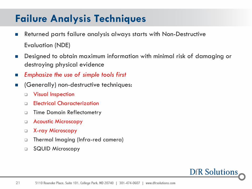
Failure Analysis Techniques
Returned parts failure analysis always starts with Non-Destructive
Evaluation (NDE) Designed to obtain maximum information with minimal risk of damaging or
destroying physical evidence
Emphasize the use of simple tools first
(Generally) non-destructive techniques:
Visual Inspection
Electrical Characterization
Time Domain Reflectometry
Acoustic Microscopy
X-ray Microscopy
Thermal Imaging (Infra-red camera)
SQUID Microscopy
22 22
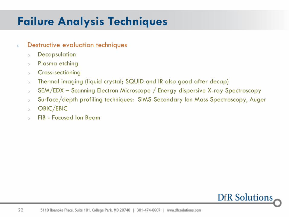
Failure Analysis Techniques
o Destructive evaluation techniques
o Decapsulation
o Plasma etching
o Cross-sectioning
o Thermal imaging (liquid crystal; SQUID and IR also good after decap)
o SEM/EDX – Scanning Electron Microscope / Energy dispersive X-ray Spectroscopy
o Surface/depth profiling techniques: SIMS-Secondary Ion Mass Spectroscopy, Auger
o OBIC/EBIC
o FIB - Focused Ion Beam
23 23
Electrical Characterization: Components
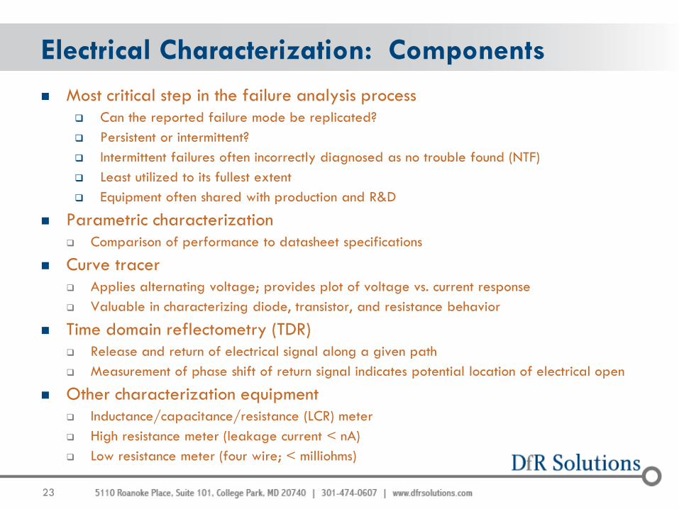
Most critical step in the failure analysis process
Can the reported failure mode be replicated?
Persistent or intermittent?
Intermittent failures often incorrectly diagnosed as no trouble found (NTF)
Least utilized to its fullest extent
Equipment often shared with production and R&D
Parametric characterization
Comparison of performance to datasheet specifications
Curve tracer
Applies alternating voltage; provides plot of voltage vs. current response
Valuable in characterizing diode, transistor, and resistance behavior
Time domain reflectometry (TDR)
Release and return of electrical signal along a given path
Measurement of phase shift of return signal indicates potential location of electrical open
Other characterization equipment
Inductance/capacitance/resistance (LCR) meter
High resistance meter (leakage current < nA)
Low resistance meter (four wire; < milliohms)
24
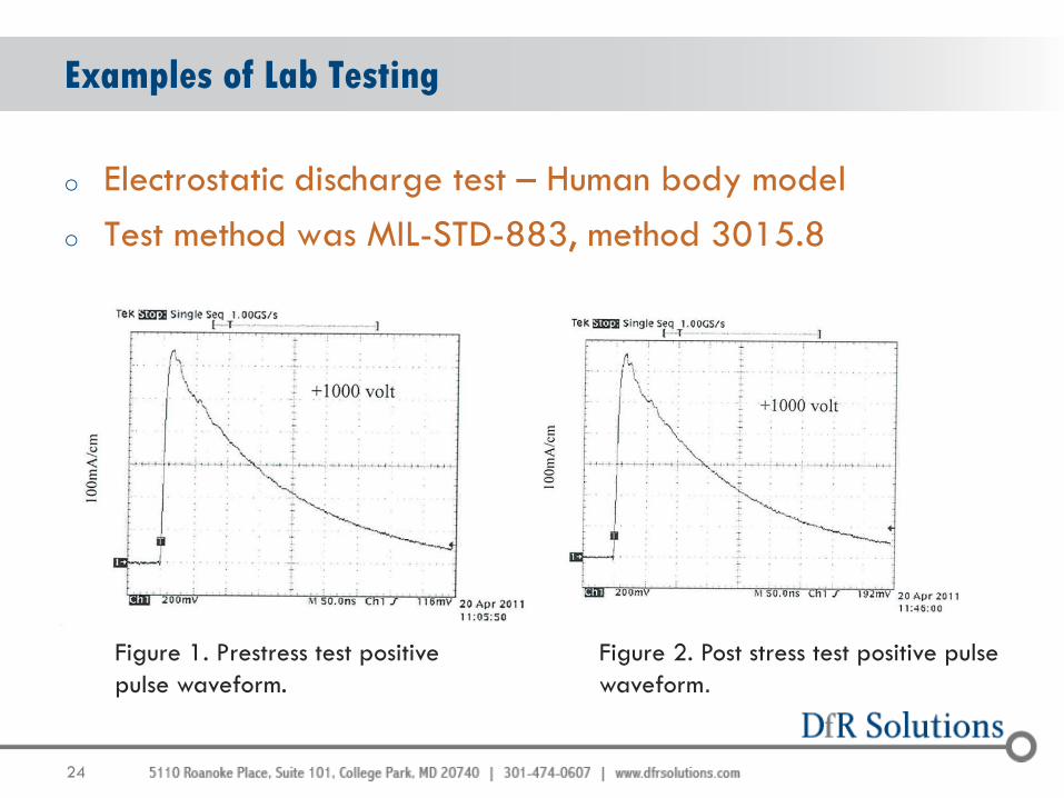
o Electrostatic discharge test – Human body model
o Test method was MIL-STD-883, method 3015.8
Examples of Lab Testing
Figure 1. Prestress test positive
pulse waveform.
Figure 2. Post stress test positive pulse
waveform.
25
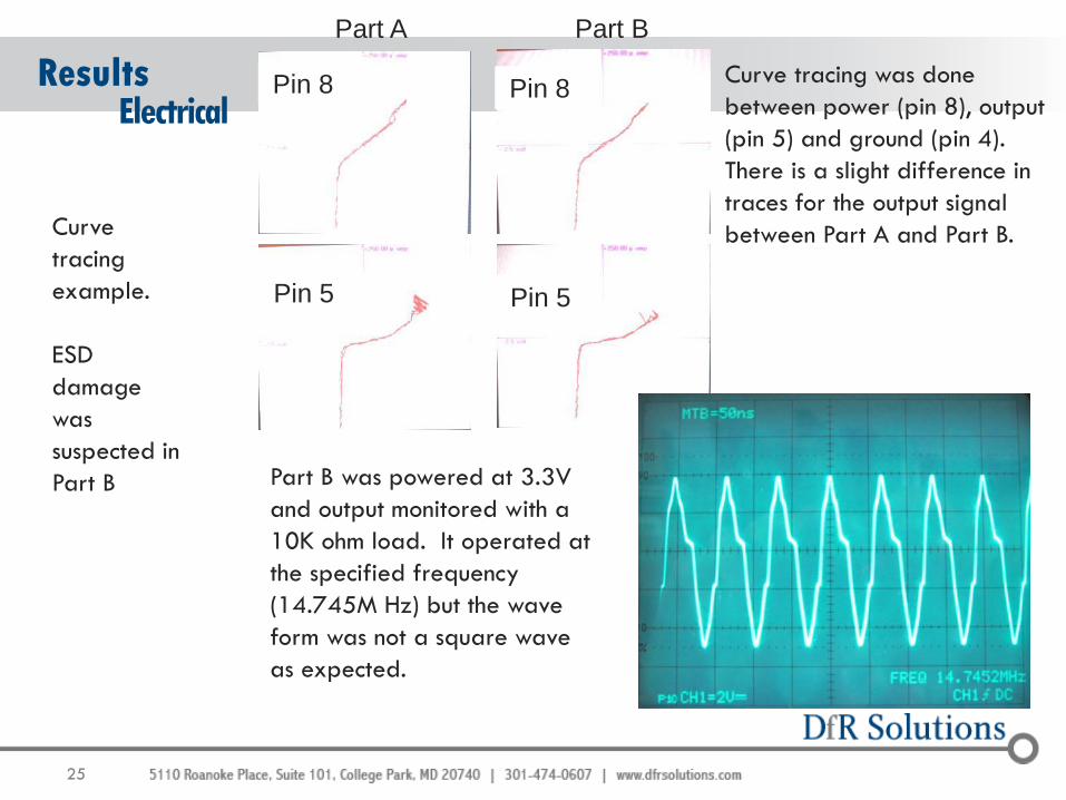
Results
Electrical Pin 8
Pin 5
Part A Part B
Pin 8
Pin 5
Curve tracing was done
between power (pin 8), output
(pin 5) and ground (pin 4).
There is a slight difference in
traces for the output signal
between Part A and Part B.
Part B was powered at 3.3V
and output monitored with a
10K ohm load. It operated at
the specified frequency
(14.745M Hz) but the wave
form was not a square wave
as expected.
Curve
tracing
example.
ESD
damage
was
suspected in
Part B
26
o Often difficult to distinguish between EOS/EOL (electrical overstress and electrical overload) and ESD. Some rules of thumb:
o ESD damage
o Small failure sites
o Not always visible without deprocessing
o No visible evidence at the package level
o EOS damage
o Large areas of damage
o Burned silicon and metallization
o Sometime visibly evident package damage
Trying to distinguish between EOS & ESD
27
o EOS: Thermal overstress to a component’s circuitry
o Short Pulse Width Failure – Junction Spiking
o Long Pulse Width Failures – Melted metallization and open
bond wires
o Junction spiking occurs when the amount of Al migration into
the silicon substrate has reached the point wherein the Al has
penetrated deep enough so as to short a p-n junction in its
path. By that time an Al spike is said to have shorted the
junction, damaging the device permanently.
Trying to distinguish between EOS & ESD
28
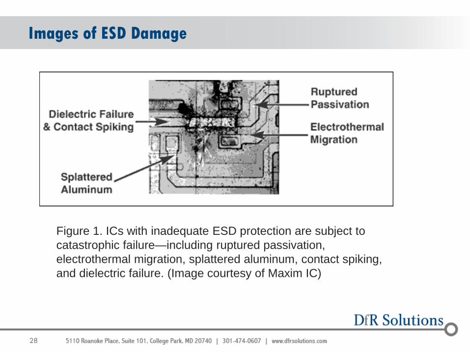
Images of ESD Damage
Figure 1. ICs with inadequate ESD protection are subject to
catastrophic failure—including ruptured passivation,
electrothermal migration, splattered aluminum, contact spiking,
and dielectric failure. (Image courtesy of Maxim IC)
29
Latent Failures
o ESD events not only impact assembly yields, but also can produce device damage that escapes testing and causes latent failures in the field.
o Devices with latent ESD defects have been referred to as “walking wounded” because they are degraded but still function
o Latent damage can occur when an ESD event is not sufficiently strong to destroy a device
o Device continues to function and is still within data-sheet limits
o Device can be subjected to numerous weak ESD events, with each new event further degrading a device until total failure
o No known practical way to screen for walking wounded devices
o Damage to insulators: weakening of the insulator structures, leading to accelerated breakdown and/or increased leakage
o Damage to junctions: lowering the lifetime of minority carriers with consequent bipolar transistor gain loss; increasing resistance in forward biased state; increasing leakage in reverse biased state
o Damage to metallization: weakening of the conductor, leading to increased resistance or increased rate of electromigration
ESD Failures: Latent Failures
30
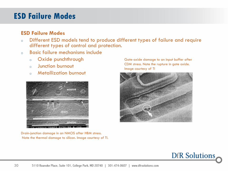
ESD Failure Modes
o Different ESD models tend to produce different types of failure and require different types of control and protection.
o Basic failure mechanisms include
o Oxide punchthrough
o Junction burnout
o Metallization burnout
Drain-junction damage in an NMOS after HBM stress.
Note the thermal damage to silicon. Image courtesy of TI.
ESD Failure Modes
Gate-oxide damage to an input buffer after
CDM stress. Note the rupture in gate oxide.
Image courtesy of TI
31
Commonly used Failure Analysis Equipment
32 32
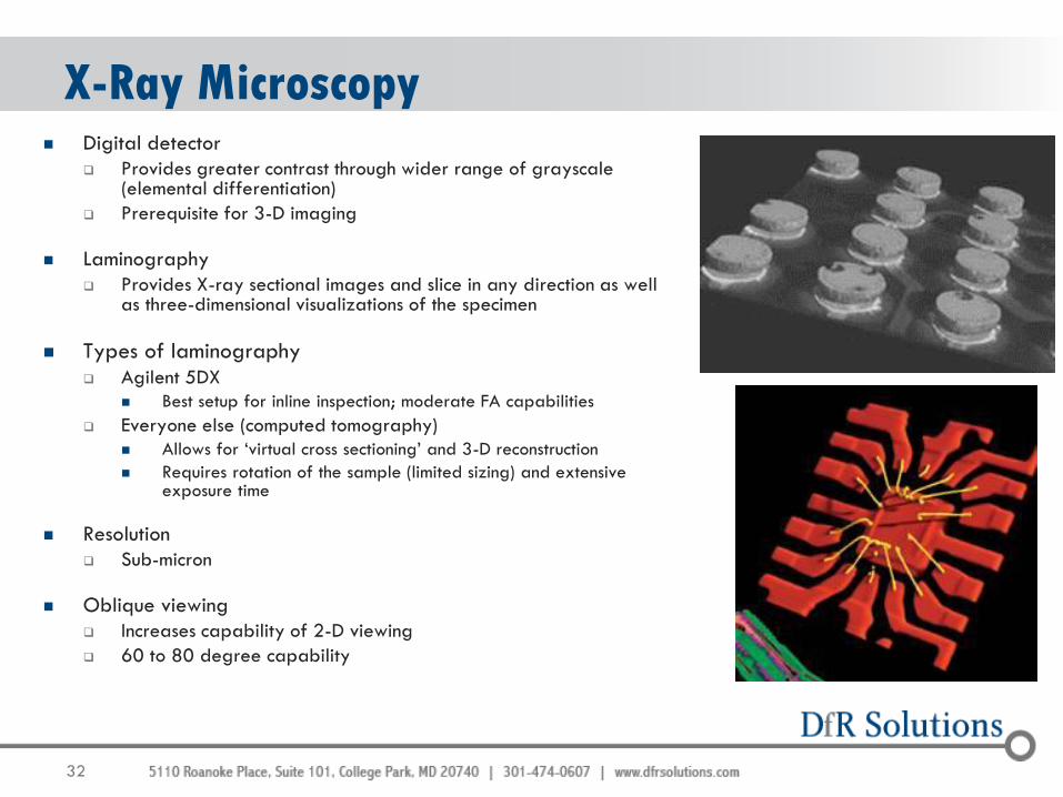
X-Ray Microscopy Digital detector
Provides greater contrast through wider range of grayscale (elemental differentiation)
Prerequisite for 3-D imaging
Laminography
Provides X-ray sectional images and slice in any direction as well as three-dimensional visualizations of the specimen
Types of laminography Agilent 5DX
Best setup for inline inspection; moderate FA capabilities
Everyone else (computed tomography)
Allows for ‘virtual cross sectioning’ and 3-D reconstruction
Requires rotation of the sample (limited sizing) and extensive exposure time
Resolution
Sub-micron
Oblique viewing
Increases capability of 2-D viewing
60 to 80 degree capability
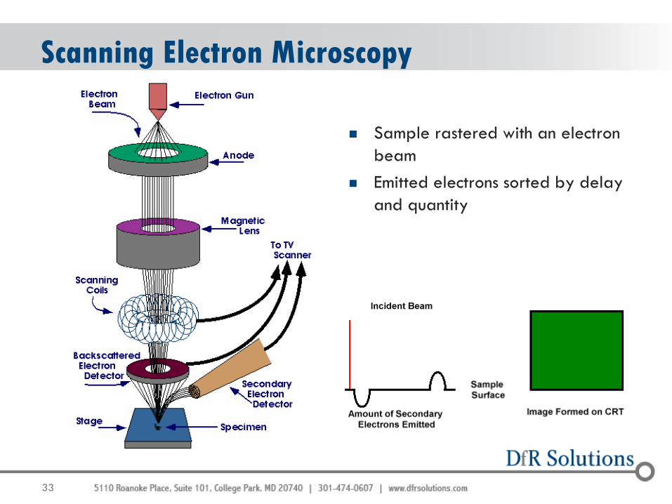
33 33
Scanning Electron Microscopy
Sample rastered with an electron
beam
Emitted electrons sorted by delay
and quantity
34 34
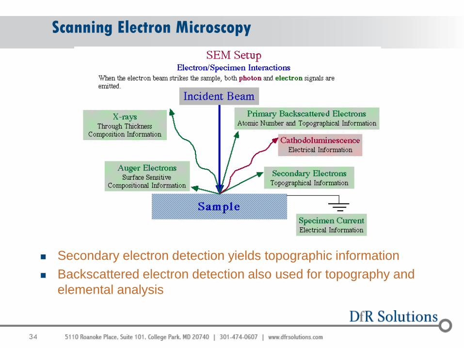
Scanning Electron Microscopy
Secondary electron detection yields topographic information
Backscattered electron detection also used for topography and
elemental analysis
35 35
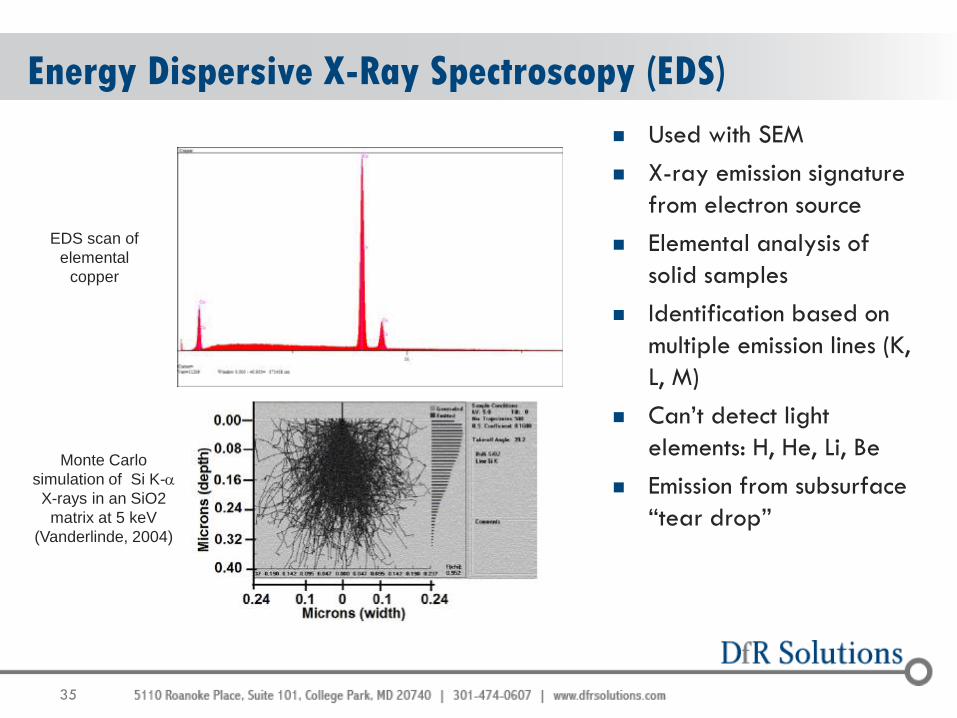
Energy Dispersive X-Ray Spectroscopy (EDS)
Used with SEM
X-ray emission signature
from electron source
Elemental analysis of
solid samples
Identification based on
multiple emission lines (K,
L, M)
Can’t detect light
elements: H, He, Li, Be
Emission from subsurface
“tear drop”
EDS scan of
elemental
copper
Monte Carlo
simulation of Si K-a
X-rays in an SiO2
matrix at 5 keV
(Vanderlinde, 2004)
36 36
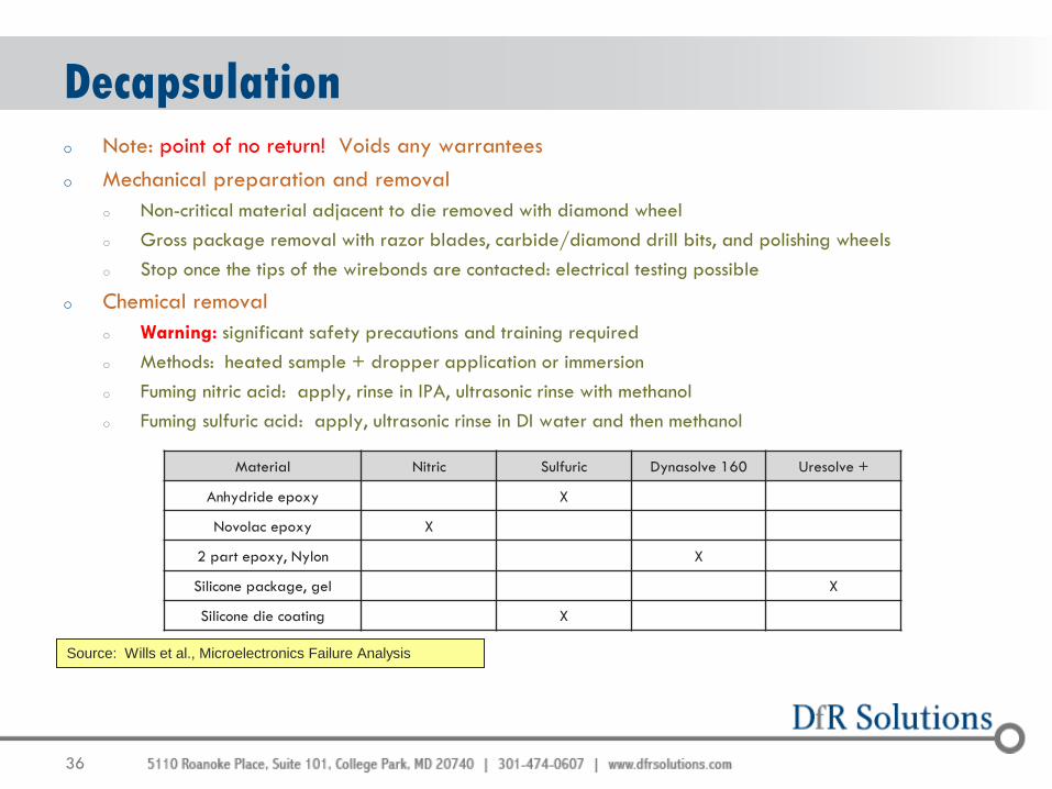
Decapsulation o Note: point of no return! Voids any warrantees
o Mechanical preparation and removal
o Non-critical material adjacent to die removed with diamond wheel
o Gross package removal with razor blades, carbide/diamond drill bits, and polishing wheels
o Stop once the tips of the wirebonds are contacted: electrical testing possible
o Chemical removal
o Warning: significant safety precautions and training required
o Methods: heated sample + dropper application or immersion
o Fuming nitric acid: apply, rinse in IPA, ultrasonic rinse with methanol
o Fuming sulfuric acid: apply, ultrasonic rinse in DI water and then methanol
Material Nitric Sulfuric Dynasolve 160 Uresolve +
Anhydride epoxy X
Novolac epoxy X
2 part epoxy, Nylon X
Silicone package, gel X
Silicone die coating X
Source: Wills et al., Microelectronics Failure Analysis
37 37
Cross-Sectioning
o Standard method for destructive subsurface evaluation
o Method:
o Cleaving/sawing to approximate area of interest
o Potting in epoxy resins to aid polishing
o Polishing medium dependent upon materials: typically diamond, SiC, or
alumina suspensions & embedded polishing cloths
o Coarse to fine (600 grit to 0.05 um) grinding sequence to eliminate
damage from previous step
o Final etch often used for microstructural relief
o Optical/electron microscopy techniques used for inspection thereafter
38 38
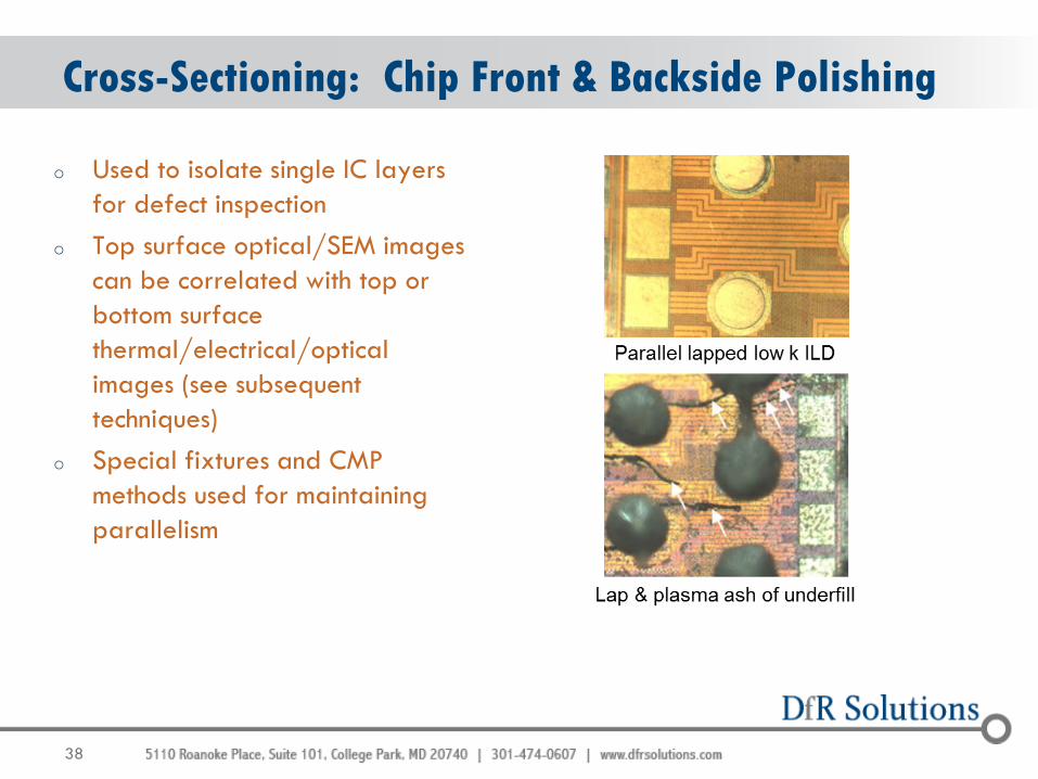
Cross-Sectioning: Chip Front & Backside Polishing
o Used to isolate single IC layers
for defect inspection
o Top surface optical/SEM images
can be correlated with top or
bottom surface
thermal/electrical/optical
images (see subsequent
techniques)
o Special fixtures and CMP
methods used for maintaining
parallelism
39 39
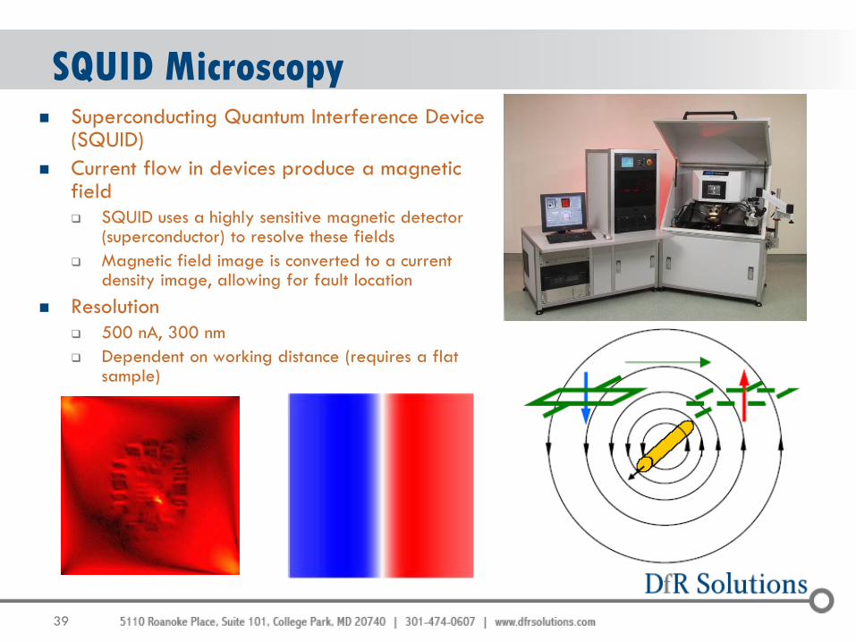
SQUID Microscopy Superconducting Quantum Interference Device
(SQUID)
Current flow in devices produce a magnetic field
SQUID uses a highly sensitive magnetic detector (superconductor) to resolve these fields
Magnetic field image is converted to a current density image, allowing for fault location
Resolution
500 nA, 300 nm
Dependent on working distance (requires a flat sample)
40 40
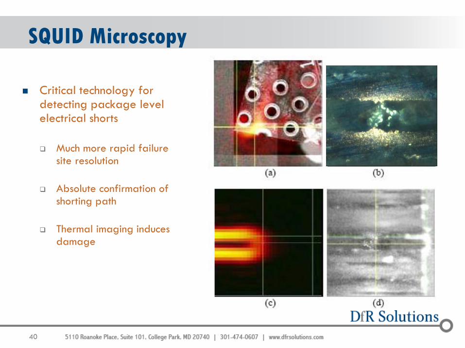
SQUID Microscopy
Critical technology for detecting package level electrical shorts
Much more rapid failure site resolution
Absolute confirmation of shorting path
Thermal imaging induces damage
41 41
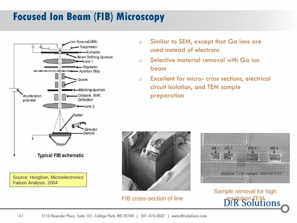
Focused Ion Beam (FIB) Microscopy
o Similar to SEM, except that Ga ions are
used instead of electrons
o Selective material removal with Ga ion
beam
o Excellent for micro- cross sections, electrical
circuit isolation, and TEM sample
preparation
FIB cross-section of line
Sample removal for high
resolution TEM
Source: Hooghan, Microelectronics
Failure Analysis, 2004
42 42
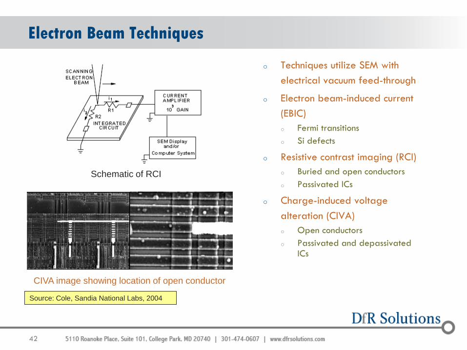
Electron Beam Techniques
o Techniques utilize SEM with
electrical vacuum feed-through
o Electron beam-induced current
(EBIC)
o Fermi transitions
o Si defects
o Resistive contrast imaging (RCI)
o Buried and open conductors
o Passivated ICs
o Charge-induced voltage
alteration (CIVA)
o Open conductors
o Passivated and depassivated ICs
Schematic of RCI
CIVA image showing location of open conductor
Source: Cole, Sandia National Labs, 2004
43 43
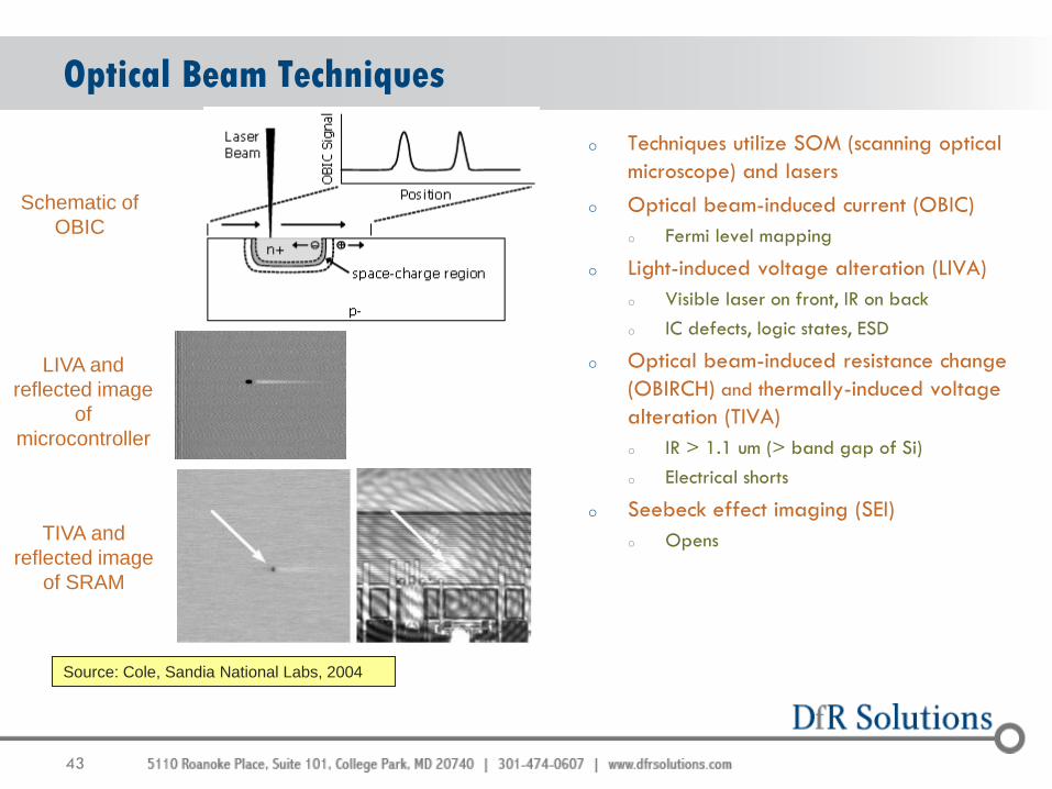
Optical Beam Techniques
Source: Cole, Sandia National Labs, 2004
o Techniques utilize SOM (scanning optical
microscope) and lasers
o Optical beam-induced current (OBIC)
o Fermi level mapping
o Light-induced voltage alteration (LIVA)
o Visible laser on front, IR on back
o IC defects, logic states, ESD
o Optical beam-induced resistance change
(OBIRCH) and thermally-induced voltage
alteration (TIVA)
o IR > 1.1 um (> band gap of Si)
o Electrical shorts
o Seebeck effect imaging (SEI)
o Opens
Schematic of
OBIC
LIVA and
reflected image
of
microcontroller
TIVA and
reflected image
of SRAM

44
Contact Information
o Questions?
o Contact Cheryl Tulkoff, [email protected],
512-913-8624
o www.dfrsolutions.com
o Connect with me in LinkedIn as well!
45
Your Partner Throughout
the Product Life Cycle
46
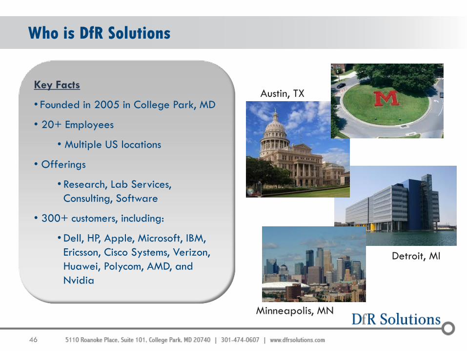
Who is DfR Solutions
Key Facts
• Founded in 2005 in College Park, MD
• 20+ Employees
• Multiple US locations
• Offerings
• Research, Lab Services,
Consulting, Software
• 300+ customers, including:
•Dell, HP, Apple, Microsoft, IBM,
Ericsson, Cisco Systems, Verizon,
Huawei, Polycom, AMD, and
Nvidia
Austin, TX
Detroit, MI
Minneapolis, MN
47
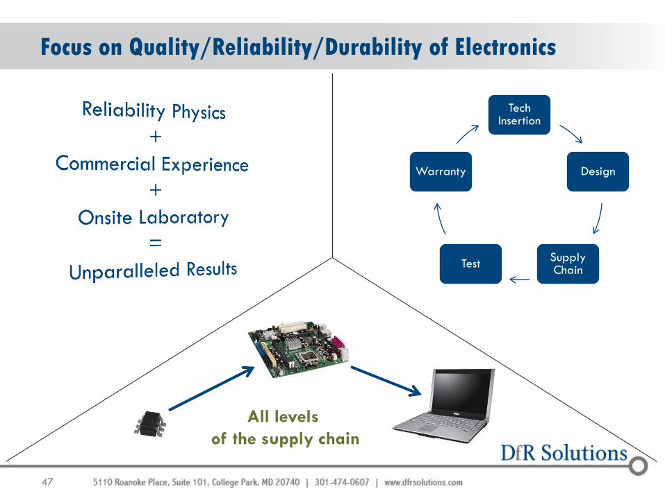
Tech Insertion
Design
Supply Chain
Test
Warranty
Focus on Quality/Reliability/Durability of Electronics
All levels
of the supply chain
48
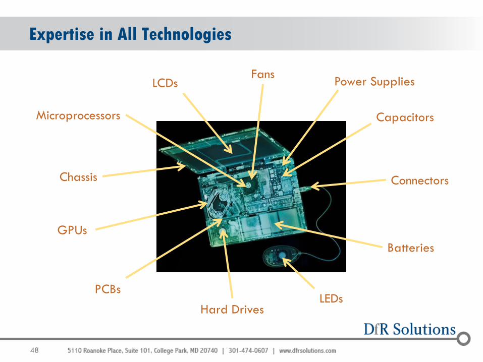
Expertise in All Technologies
LCDs
Chassis
Microprocessors
Batteries
Fans Power Supplies
Hard Drives
PCBs
Capacitors
LEDs
Connectors
GPUs

49
Our Customers (over 400 and growing)
50
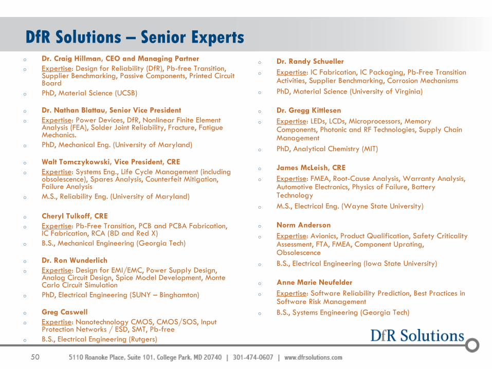
DfR Solutions – Senior Experts o Dr. Craig Hillman, CEO and Managing Partner
o Expertise: Design for Reliability (DfR), Pb-free Transition, Supplier Benchmarking, Passive Components, Printed Circuit Board
o PhD, Material Science (UCSB)
o Dr. Nathan Blattau, Senior Vice President
o Expertise: Power Devices, DfR, Nonlinear Finite Element Analysis (FEA), Solder Joint Reliability, Fracture, Fatigue Mechanics.
o PhD, Mechanical Eng. (University of Maryland)
o Walt Tomczykowski, Vice President, CRE
o Expertise: Systems Eng., Life Cycle Management (including obsolescence), Spares Analysis, Counterfeit Mitigation, Failure Analysis
o M.S., Reliability Eng. (University of Maryland)
o Cheryl Tulkoff, CRE
o Expertise: Pb-Free Transition, PCB and PCBA Fabrication, IC Fabrication, RCA (8D and Red X)
o B.S., Mechanical Engineering (Georgia Tech)
o Dr. Ron Wunderlich
o Expertise: Design for EMI/EMC, Power Supply Design, Analog Circuit Design, Spice Model Development, Monte Carlo Circuit Simulation
o PhD, Electrical Engineering (SUNY – Binghamton)
o Greg Caswell
o Expertise: Nanotechnology CMOS, CMOS/SOS, Input Protection Networks / ESD, SMT, Pb-free
o B.S., Electrical Engineering (Rutgers)
o Dr. Randy Schueller
o Expertise: IC Fabrication, IC Packaging, Pb-Free Transition Activities, Supplier Benchmarking, Corrosion Mechanisms
o PhD, Material Science (University of Virginia)
o Dr. Gregg Kittlesen
o Expertise: LEDs, LCDs, Microprocessors, Memory Components, Photonic and RF Technologies, Supply Chain Management
o PhD, Analytical Chemistry (MIT)
o James McLeish, CRE
o Expertise: FMEA, Root-Cause Analysis, Warranty Analysis, Automotive Electronics, Physics of Failure, Battery Technology
o M.S., Electrical Eng. (Wayne State University)
o Norm Anderson
o Expertise: Avionics, Product Qualification, Safety Criticality Assessment, FTA, FMEA, Component Uprating, Obsolescence
o B.S., Electrical Engineering (Iowa State University)
o Anne Marie Neufelder
o Expertise: Software Reliability Prediction, Best Practices in Software Risk Management
o B.S., Systems Engineering (Georgia Tech)
51
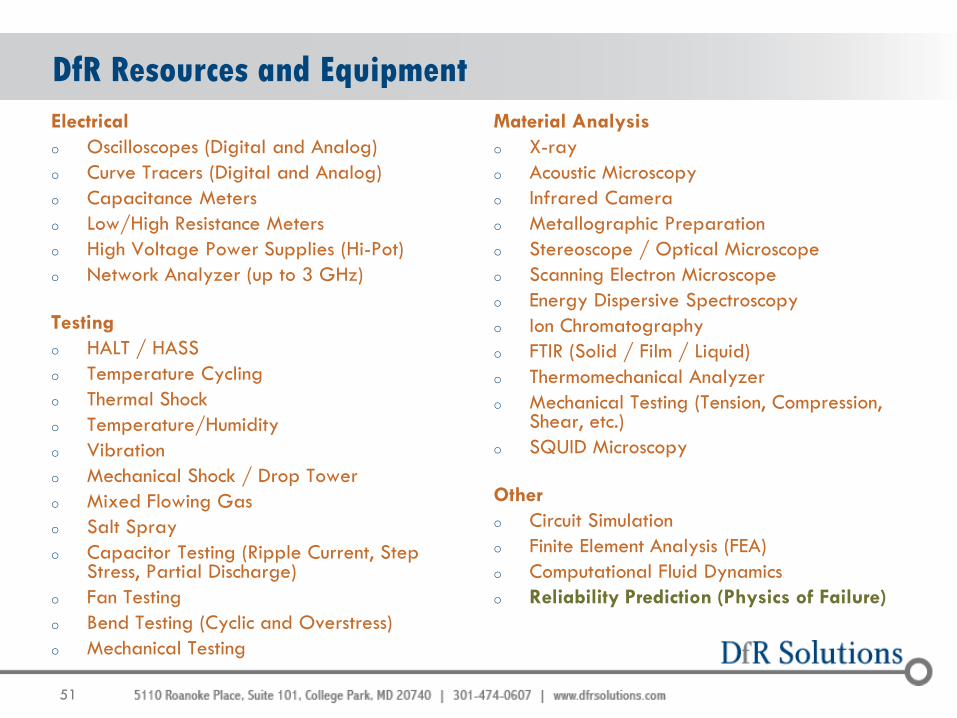
DfR Resources and Equipment
Electrical
o Oscilloscopes (Digital and Analog)
o Curve Tracers (Digital and Analog)
o Capacitance Meters
o Low/High Resistance Meters
o High Voltage Power Supplies (Hi-Pot)
o Network Analyzer (up to 3 GHz)
Testing
o HALT / HASS
o Temperature Cycling
o Thermal Shock
o Temperature/Humidity
o Vibration
o Mechanical Shock / Drop Tower
o Mixed Flowing Gas
o Salt Spray
o Capacitor Testing (Ripple Current, Step Stress, Partial Discharge)
o Fan Testing
o Bend Testing (Cyclic and Overstress)
o Mechanical Testing
Material Analysis
o X-ray
o Acoustic Microscopy
o Infrared Camera
o Metallographic Preparation
o Stereoscope / Optical Microscope
o Scanning Electron Microscope
o Energy Dispersive Spectroscopy
o Ion Chromatography
o FTIR (Solid / Film / Liquid)
o Thermomechanical Analyzer
o Mechanical Testing (Tension, Compression, Shear, etc.)
o SQUID Microscopy
Other
o Circuit Simulation
o Finite Element Analysis (FEA)
o Computational Fluid Dynamics
o Reliability Prediction (Physics of Failure)
52
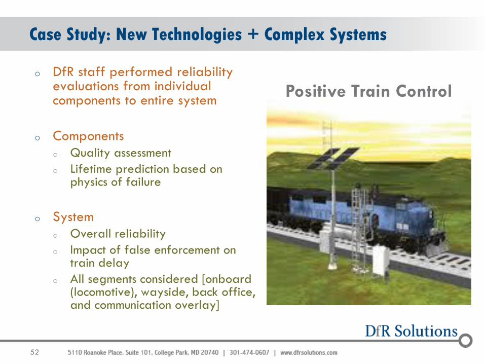
o DfR staff performed reliability evaluations from individual components to entire system
o Components
o Quality assessment
o Lifetime prediction based on physics of failure
o System
o Overall reliability
o Impact of false enforcement on train delay
o All segments considered [onboard (locomotive), wayside, back office, and communication overlay]
Case Study: New Technologies + Complex Systems
Positive Train Control
53
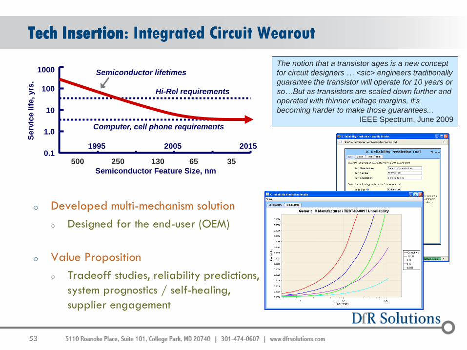
o Developed multi-mechanism solution
o Designed for the end-user (OEM)
o Value Proposition
o Tradeoff studies, reliability predictions,
system prognostics / self-healing,
supplier engagement
Tech Insertion: Integrated Circuit Wearout
The notion that a transistor ages is a new concept
for circuit designers … <sic> engineers traditionally
guarantee the transistor will operate for 10 years or
so…But as transistors are scaled down further and
operated with thinner voltage margins, it’s
becoming harder to make those guarantees...
IEEE Spectrum, June 2009
1995 2005 2015 0.1
1.0
10
100
1000
Se
rvic
e lif
e,
yrs
.
Computer, cell phone requirements
Hi-Rel requirements
500 250 130 65 35
Semiconductor lifetimes
Semiconductor Feature Size, nm
54
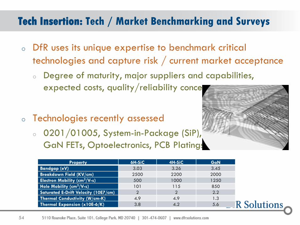
o DfR uses its unique expertise to benchmark critical
technologies and capture risk / current market acceptance
o Degree of maturity, major suppliers and capabilities,
expected costs, quality/reliability concerns
o Technologies recently assessed
o 0201/01005, System-in-Package (SiP),
GaN FETs, Optoelectronics, PCB Platings
Tech Insertion: Tech / Market Benchmarking and Surveys
Property 6H-SiC 4H-SiC GaN
Bandgap (eV) 3.03 3.26 3.45
Breakdown Field (KV/cm) 2500 2200 2000
Electron Mobility (cm2/V-s) 500 1000 1250
Hole Mobility (cm2/V-s) 101 115 850
Saturated E-Drift Velocity (10E7/cm) 2 2 2.2
Thermal Conductivity (W/cm-K) 4.9 4.9 1.3
Thermal Expansion (x10E-6/K) 3.8 4.2 5.6
55
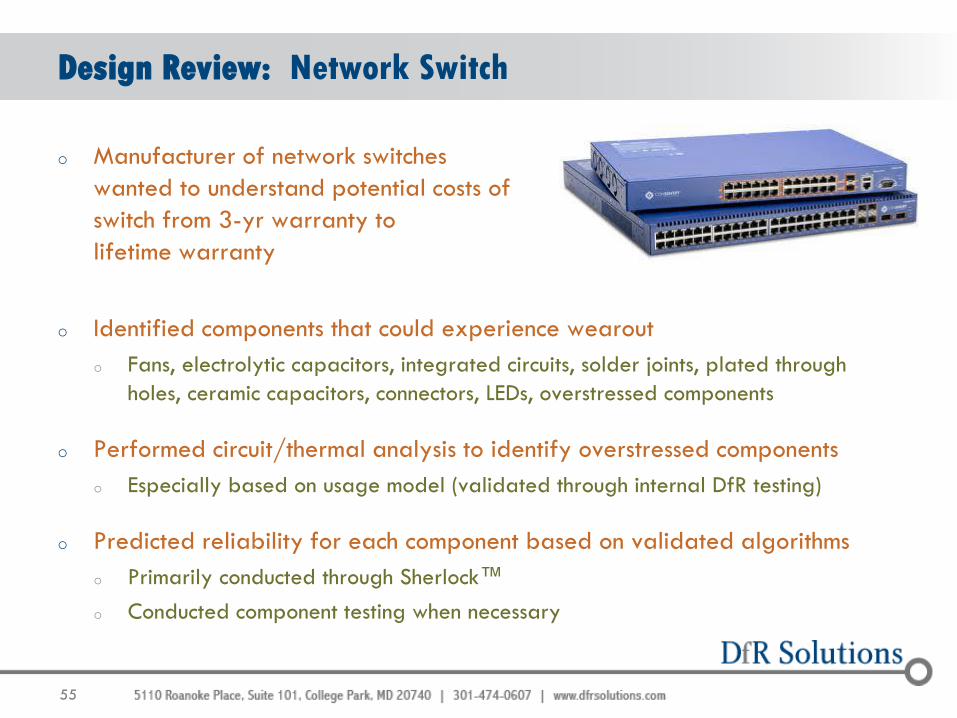
o Manufacturer of network switches
wanted to understand potential costs of
switch from 3-yr warranty to
lifetime warranty
o Identified components that could experience wearout
o Fans, electrolytic capacitors, integrated circuits, solder joints, plated through
holes, ceramic capacitors, connectors, LEDs, overstressed components
o Performed circuit/thermal analysis to identify overstressed components
o Especially based on usage model (validated through internal DfR testing)
o Predicted reliability for each component based on validated algorithms
o Primarily conducted through Sherlock™
o Conducted component testing when necessary
Design Review: Network Switch
56
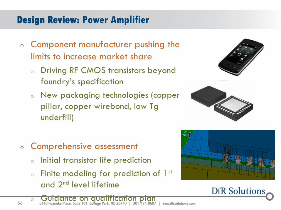
o Component manufacturer pushing the
limits to increase market share
o Driving RF CMOS transistors beyond
foundry’s specification
o New packaging technologies (copper
pillar, copper wirebond, low Tg
underfill)
o Comprehensive assessment
o Initial transistor life prediction
o Finite modeling for prediction of 1st
and 2nd level lifetime
o Guidance on qualification plan
Design Review: Power Amplifier
57
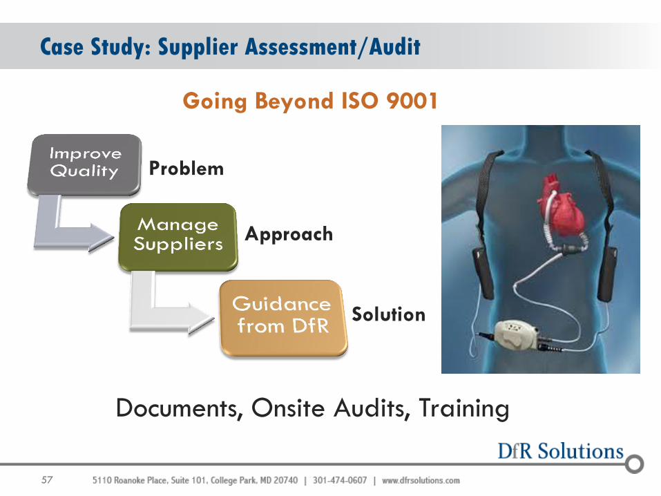
Case Study: Supplier Assessment/Audit
Going Beyond ISO 9001
Problem
Approach
Solution
Documents, Onsite Audits, Training
58
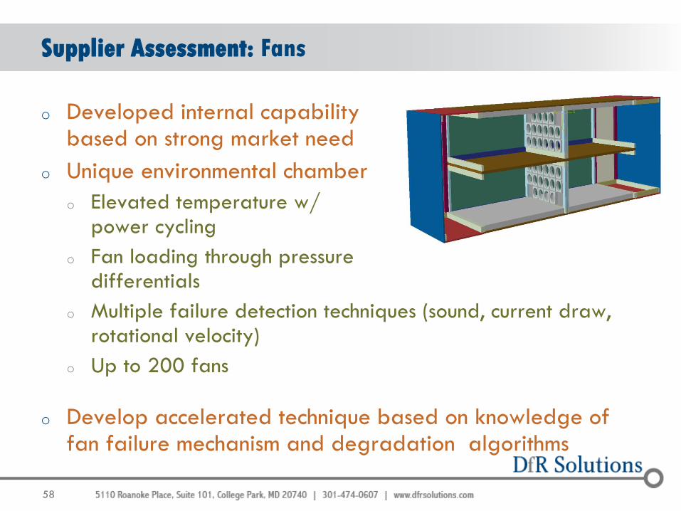
o Developed internal capability based on strong market need
o Unique environmental chamber
o Elevated temperature w/ power cycling
o Fan loading through pressure differentials
o Multiple failure detection techniques (sound, current draw, rotational velocity)
o Up to 200 fans
o Develop accelerated technique based on knowledge of fan failure mechanism and degradation algorithms
Supplier Assessment: Fans
59
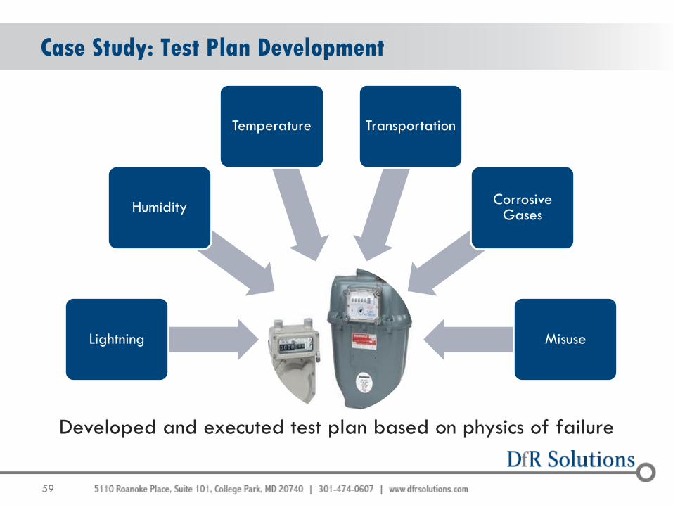
Lightning
Humidity
Temperature Transportation
Corrosive Gases
Misuse
Case Study: Test Plan Development
Developed and executed test plan based on physics of failure
60
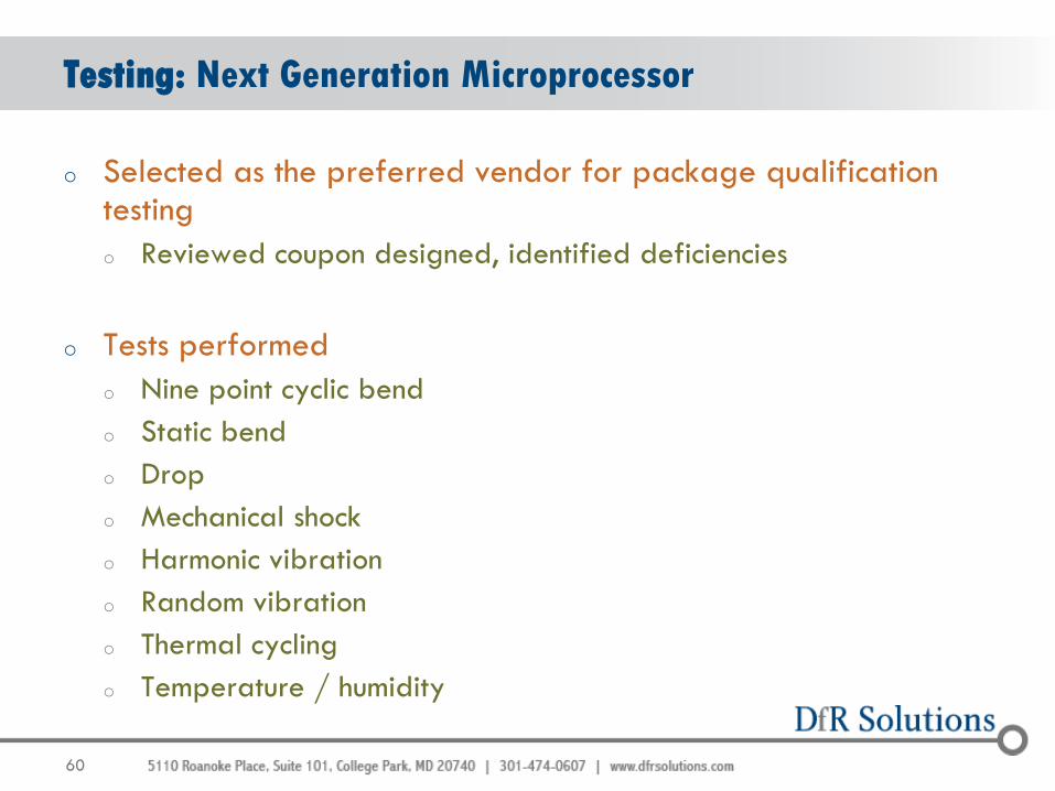
o Selected as the preferred vendor for package qualification testing
o Reviewed coupon designed, identified deficiencies
o Tests performed
o Nine point cyclic bend
o Static bend
o Drop
o Mechanical shock
o Harmonic vibration
o Random vibration
o Thermal cycling
o Temperature / humidity
Testing: Next Generation Microprocessor
61
o The number one requirement in failure analysis
o DfR has all the necessary elements
o Electrical engineers, mechanical engineers, materials
scientists, inorganic chemists, etc.
o Extensive in-house expertise
o PhD, MS, BS + industry experience
o The right background
o Over 1000 failure analyses combined
Root Cause Analysis (RCA) -- Personnel
62
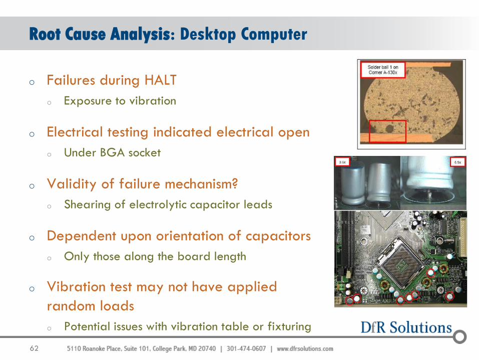
o Failures during HALT
o Exposure to vibration
o Electrical testing indicated electrical open
o Under BGA socket
o Validity of failure mechanism?
o Shearing of electrolytic capacitor leads
o Dependent upon orientation of capacitors
o Only those along the board length
o Vibration test may not have applied
random loads
o Potential issues with vibration table or fixturing
Root Cause Analysis: Desktop Computer
63
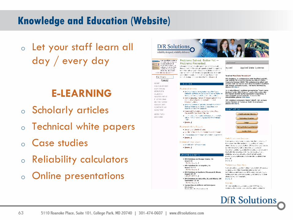
o Let your staff learn all
day / every day
E-LEARNING
o Scholarly articles
o Technical white papers
o Case studies
o Reliability calculators
o Online presentations
Knowledge and Education (Website)
64
o Could your next product benefit from DfR’s extensive expertise
and PoF knowledge base?
o Bring us in as an independent party during critical design reviews
o Are your concerned with new technologies?
o DfR’s scientists and engineers can provide comprehensive analysis to ensure risk-
minimization during these difficult transitions
o Take advantage of our unique Open-Door policy!
o See how much we already know about your current issues
o Chances are we have already solved your problem at least once before
o We work around the clock and around the world
o Contact us by phone (301-474-0607) or email ([email protected])
Interested?


![Prevention of Worsening Heart Failure by Serelaxin in ... Failure/RELAX-AHF (2)].pdf · Prevention of Worsening Heart Failure by Serelaxin in Patients Admitted for Acute Heart Failure:](https://static.cupdf.com/doc/110x72/5cce5b0088c9934c718cf98b/prevention-of-worsening-heart-failure-by-serelaxin-in-failurerelax-ahf-2pdf.jpg)