itif cn e Ci oc nS fl ea rn eo ni ct ea 2nr 0e 1t 1nI
ISC 2011
Proceeding of the International Conference on Advanced Science, Engineering and Information Technology 2011
Hotel Equatorial Bangi-Putrajaya, Malaysia, 14 - 15 January 2011
ISBN 978-983-42366-4-9
ISC 2011
International Conference on Advanced Science,Engineering and Information Technology
ICASEIT 2011
Cutting Edge Sciences for Future Sustainability
Hotel Equatorial Bangi-Putrajaya, Malaysia, 14 - 15 January 2011
SRI EA V IUN
ITN IES
ED KOBIN
NR A
GJA
AL SA
AE
N P
M N
AA
LU
AT
YA
SS
AI
RE
P
NINO O
D
I TA ENI CO AI S
SSA TS NSTNEDU
Organized by Indonesian Students AssociationUniversiti Kebangsaan Malaysia
Proceeding of the
Comparative Study of 4-Switch Buck-Boost
Controller and Regular Buck-Boost Taufik Taufik
#, Justin Arakaki
#, Dale Dolan
#, Makbul Anwari
*
# Electrical Engineering Department, Cal Poly State University
1 Grand Avenue, San Luis Obispo, CA 93407, USA
Tel.:+18057562318, E-mail: [email protected]
*Faculty of Electrical Engineering, Universiti Teknologi Malaysia
81310 UTM Skudai, Malaysia
Abstract— A very important characteristic that dc-dc converters require is the ability to efficiently regulate an output voltage with a
wide ranging value of input voltages. A recently developed solution to this requirement is a synchronous 4-Switch Buck-Boost
controller developed by Linear Technology. The Linear Technology’s LTC3780 controller chip enables the adoption of a 4-Switch
switching topology as opposed to the traditional single-switch Buck-Boost topology. In this paper, the LTC3780’s 4-Switch Buck-
Boost topology is analyzed and its performance is compared against those of the regular single-switch Buck-Boost topology. Results
from computer simulations demonstrate the benefits of using the 4-switch approach than the conventional buck-boost method.
Keywords—Buck-boost, 4-Switch buck-boost, controller.
I. INTRODUCTION
Many applications require a dc-dc converter that is able to
regulate its output voltage from a wide range of input
voltages. These applications often require the output voltage
to be higher than, lower than, or approximately equal to the
input voltage. By utilizing a buck-boost topology, the input
voltage can be either stepped-up or stepped-down to the
desired voltage [1]. However, there are several unwanted
characteristics that come with the basic topology of a buck-
boost converter. Some problems include mediocre efficiency,
polarity inversion of the output voltage relative to the input
voltage, bad input current characteristics, and bad output
current characteristics.
To counter these drawbacks, several existing options are
available. Instead of using the traditional 1-switch buck-
boost topology, a 4-switch Buck-Boost topology has been
found to seamlessly transition between true synchronous
buck and boost, depending on the input voltage, which in
turn increases efficiency amongst other things [2][3].
Analysis of Linear’s LTC3780 controller chip, the industry’s
first FSBB Controller using a single inductor, will be done
and compared to the classic single switch buck-boost
topology of LT3430 [4].
II. SINGLE-SWITCH BUCK-BOOST CONVERTER
Figure 1 displays the traditional Buck-Boost topology
which utilizes a single switch, an inductor, a diode, and a
single output capacitor. This Buck-Boost converter topology
uses the same amount of components as the Buck and the
Boost converters; the only difference is the components are
arranged differently [5].
The output voltage can be either higher or lower than the
input voltage, hence the name Buck-Boost Converter.
Fig. 1 Traditional Buck-Boost Topology using a Single-Switch
A. Operation
The Buck-Boost has two different states in which it
operates. The two states are distinguished between each
other with the switch being CLOSED or in the OPEN
position [6].
441
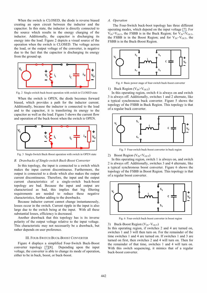
When the switch is CLOSED, the diode is reverse biased
creating an open circuit between the inductor and the
capacitor. In this state, the inductor is directly connected to
the source which results in the energy charging of the
inductor. Additionally, the capacitor is discharging its
energy into the load. Figure 2 depicts a visual source of the
operation when the switch is CLOSED. The voltage across
the load, or the output voltage of the converter, is negative
due to the fact that the capacitor is discharging its energy
from the ground up.
Fig. 2 Single-switch buck-boost operation with switch in CLOSED state
When the switch is OPEN, the diode becomes forward
biased, which provides a path for the inductor current.
Additionally, because the inductor is connected to the load
and to the capacitor, it is transferring its energy to the
capacitor as well as the load. Figure 3 shows the current flow
and operation of the buck-boost when the switch is OPEN.
Fig. 3 Single-Switch Buck-Boost operation with switch in OPEN state
B. Drawbacks of Single-switch Buck-Boost Converter
In this topology, the input is connected to a switch which
makes the input current discontinuous. Furthermore, the
output is connected to a diode which also makes the output
current discontinuous. Therefore, the input and the output
current characteristics of a single-switch buck-boost
topology are bad. Because the input and output are
characterized as bad, this implies that big filtering
requirements are needed to reduce these negative
characteristics, further adding to the drawbacks.
Because inductor current cannot change instantaneously,
losses occur in the switch. Current ripple in the input is also
large due to the switch being at the input. With all these
substantial losses, efficiency is decreased.
Another drawback that this topology has is its inverse
polarity of the output voltage relative to the input voltage.
This characteristic may not necessarily be a drawback, but
rather depends on user preference.
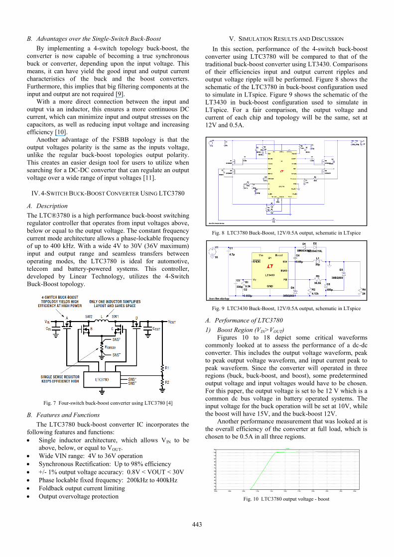
III. FOUR-SWITCH BUCK-BOOST CONVERTER
Figure 4 displays a simplified Four-Switch Buck-Boost
converter topology [7][8]. Depending upon the input
voltage, the converter is able to change its mode of operation,
either to be in buck, boost, or buck-boost.
A. Operation
The Four-Switch buck-boot topology has three different
operating modes, which depend on the input voltage [7]. For
VIN>VOUT, the FSBB is in the Buck Region; for VIN<VOUT,
the FSBB is in the Boost Region; and for VIN~VOUT, the
FSBB is in the Buck-Boost Region.
Fig. 4 Basic power stage of four-switch buck-boost converter
1) Buck Region (VIN>VOUT)
In this operating region, switch 4 is always on and switch
3 is always off. Additionally, switches 1 and 2 alternate, like
a typical synchronous buck converter. Figure 5 shows the
topology of the FSBB in Buck Region. This topology is that
of a regular buck converter.
Fig. 5 Four-switch buck-boost converter in buck region
2) Boost Region (VIN<VOUT)
In this operating region, switch 1 is always on, and switch
2 is always off. Additionally, switches 3 and 4 alternate, like
a typical synchronous boost converter. Figure 6 shows the
topology of the FSBB in Boost Region. This topology is that
of a regular boost converter.
Fig. 6 Four-switch buck-boost converter in boost region
3) Buck-Boost Region (VIN~VOUT)
In this operating region, if switches 2 and 4 are turned on,
switches 1 and 3 will then turn on. For the remainder of the
time switches 1 and 4 are turned on. If switches 1 and 3 are
turned on first, then switches 2 and 4 will turn on. Then for
the remainder of that time, switches 1 and 4 will turn on.
With this switch sequencing, it mimics that of a regular
buck-boost converter.
442
B. Advantages over the Single-Switch Buck-Boost
By implementing a 4-switch topology buck-boost, the
converter is now capable of becoming a true synchronous
buck or converter, depending upon the input voltage. This
means, it can have yield the good input and output current
characteristics of the buck and the boost converters.
Furthermore, this implies that big filtering components at the
input and output are not required [9].
With a more direct connection between the input and
output via an inductor, this ensures a more continuous DC
current, which can minimize input and output stresses on the
capacitors, as well as reducing input voltage and increasing
efficiency [10].
Another advantage of the FSBB topology is that the
output voltages polarity is the same as the inputs voltage,
unlike the regular buck-boost topologies output polarity.
This creates an easier design tool for users to utilize when
searching for a DC-DC converter that can regulate an output
voltage over a wide range of input voltages [11].
IV. 4-SWITCH BUCK-BOOST CONVERTER USING LTC3780
A. Description
The LTC®3780 is a high performance buck-boost switching
regulator controller that operates from input voltages above,
below or equal to the output voltage. The constant frequency
current mode architecture allows a phase-lockable frequency
of up to 400 kHz. With a wide 4V to 30V (36V maximum)
input and output range and seamless transfers between
operating modes, the LTC3780 is ideal for automotive,
telecom and battery-powered systems. This controller,
developed by Linear Technology, utilizes the 4-Switch
Buck-Boost topology.
Fig. 7 Four-switch buck-boost converter using LTC3780 [4]
B. Features and Functions
The LTC3780 buck-boost converter IC incorporates the
following features and functions:
Single inductor architecture, which allows VIN to be
above, below, or equal to VOUT.
Wide VIN range: 4V to 36V operation
Synchronous Rectification: Up to 98% efficiency
+/- 1% output voltage accuracy: 0.8V < VOUT < 30V
Phase lockable fixed frequency: 200kHz to 400kHz
Foldback output current limiting
Output overvoltage protection
V. SIMULATION RESULTS AND DISCUSSION
In this section, performance of the 4-switch buck-boost
converter using LTC3780 will be compared to that of the
traditional buck-boost converter using LT3430. Comparisons
of their efficiencies input and output current ripples and
output voltage ripple will be performed. Figure 8 shows the
schematic of the LTC3780 in buck-boost configuration used
to simulate in LTspice. Figure 9 shows the schematic of the
LT3430 in buck-boost configuration used to simulate in
LTspice. For a fair comparison, the output voltage and
current of each chip and topology will be the same, set at
12V and 0.5A.
Fig. 8 LTC3780 Buck-Boost, 12V/0.5A output, schematic in LTspice
Fig. 9 LTC3430 Buck-Boost, 12V/0.5A output, schematic in LTspice
A. Performance of LTC3780
1) Boost Region (VIN>VOUT)
Figures 10 to 18 depict some critical waveforms
commonly looked at to assess the performance of a dc-dc
converter. This includes the output voltage waveform, peak
to peak output voltage waveform, and input current peak to
peak waveform. Since the converter will operated in three
regions (buck, buck-boost, and boost), some predetermined
output voltage and input voltages would have to be chosen.
For this paper, the output voltage is set to be 12 V which is a
common dc bus voltage in battery operated systems. The
input voltage for the buck operation will be set at 10V, while
the boost will have 15V, and the buck-boost 12V.
Another performance measurement that was looked at is
the overall efficiency of the converter at full load, which is
chosen to be 0.5A in all three regions.
Fig. 10 LTC3780 output voltage - boost
443

Fig. 11 LTC3780 output voltage peak to peak ripple - boost
Fig. 12 LTC3780 input current peak to peak ripple - boost
2) Buck-Boost Region (VIN~VOUT)
Fig. 13 LTC3780 output voltage – buck boost
Fig. 14 LTC3780 output voltage peak to peak ripple – buck boost
Fig. 15 LTC3780 input current peak to peak ripple – buck boost
3) Buck Region (VIN>VOUT)
Fig. 16 LTC3780 output voltage – buck
Fig. 17 LTC3780 output voltage peak to peak ripple – buck
Fig. 18 LTC3780 input current peak to peak ripple – buck
B. Performance of LTC3430
1) Boost Region (VIN<VOUT)
Figures 19 to 28 depict the same critical waveforms as
obtained in the 4-switch buck-boost. Since LTC3430 is a
controller for a standard buck-boost converter, the
performance for buck, buck-boost, and boost was also
explored.
Fig. 19 LTC3430 output voltage - boost
Fig. 20 LTC3430 output voltage peak to peak ripple - boost
Fig. 21 LTC3430 input current peak to peak ripple - boost
2) Buck-Boost Region (VIN~VOUT)
Fig. 22 LTC3430 output voltage – buck boost
Fig. 23 LTC3430 output voltage peak to peak ripple – buck boost
Fig. 24 LTC3430 input current peak to peak ripple – buck boost
3) Buck Region (VIN>VOUT)
Fig. 25 LTC3430 output voltage – buck
444
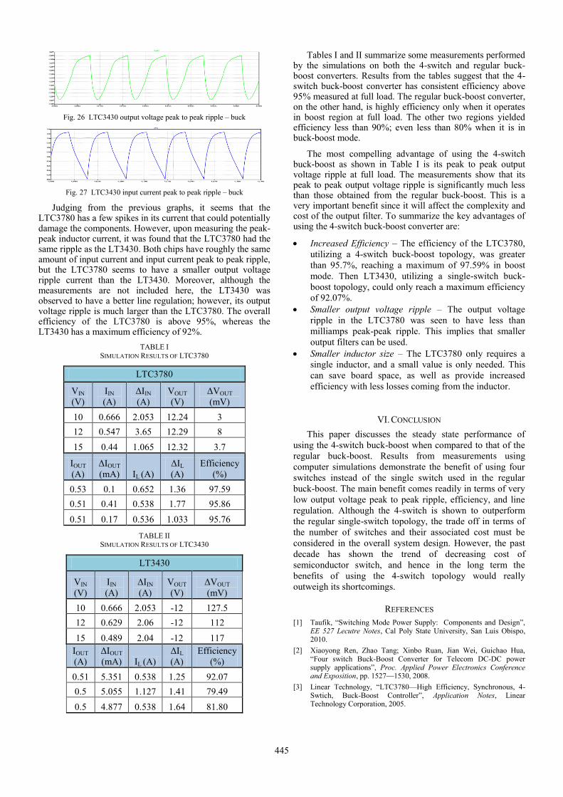
Fig. 26 LTC3430 output voltage peak to peak ripple – buck
Fig. 27 LTC3430 input current peak to peak ripple – buck
Judging from the previous graphs, it seems that the LTC3780 has a few spikes in its current that could potentially damage the components. However, upon measuring the peak-peak inductor current, it was found that the LTC3780 had the same ripple as the LT3430. Both chips have roughly the same amount of input current and input current peak to peak ripple, but the LTC3780 seems to have a smaller output voltage ripple current than the LT3430. Moreover, although the measurements are not included here, the LT3430 was observed to have a better line regulation; however, its output voltage ripple is much larger than the LTC3780. The overall efficiency of the LTC3780 is above 95%, whereas the LT3430 has a maximum efficiency of 92%.
TABLE I
SIMULATION RESULTS OF LTC3780
LTC3780
VIN
(V)
IIN
(A)
ΔIIN
(A)
VOUT
(V)
ΔVOUT
(mV)
10 0.666 2.053 12.24 3
12 0.547 3.65 12.29 8
15 0.44 1.065 12.32 3.7
IOUT
(A)
ΔIOUT
(mA) IL (A)
ΔIL
(A)
Efficiency
(%)
0.53 0.1 0.652 1.36 97.59
0.51 0.41 0.538 1.77 95.86
0.51 0.17 0.536 1.033 95.76
TABLE II
SIMULATION RESULTS OF LTC3430
LT3430
VIN
(V)
IIN
(A)
ΔIIN
(A)
VOUT
(V)
ΔVOUT
(mV)
10 0.666 2.053 -12 127.5
12 0.629 2.06 -12 112
15 0.489 2.04 -12 117
IOUT
(A)
ΔIOUT
(mA) IL (A)
ΔIL
(A)
Efficiency
(%)
0.51 5.351 0.538 1.25 92.07
0.5 5.055 1.127 1.41 79.49
0.5 4.877 0.538 1.64 81.80
Tables I and II summarize some measurements performed by the simulations on both the 4-switch and regular buck-boost converters. Results from the tables suggest that the 4-switch buck-boost converter has consistent efficiency above 95% measured at full load. The regular buck-boost converter, on the other hand, is highly efficiency only when it operates in boost region at full load. The other two regions yielded efficiency less than 90%; even less than 80% when it is in buck-boost mode.
The most compelling advantage of using the 4-switch buck-boost as shown in Table I is its peak to peak output voltage ripple at full load. The measurements show that its peak to peak output voltage ripple is significantly much less than those obtained from the regular buck-boost. This is a very important benefit since it will affect the complexity and cost of the output filter. To summarize the key advantages of using the 4-switch buck-boost converter are:
Increased Efficiency – The efficiency of the LTC3780,
utilizing a 4-switch buck-boost topology, was greater
than 95.7%, reaching a maximum of 97.59% in boost
mode. Then LT3430, utilizing a single-switch buck-
boost topology, could only reach a maximum efficiency
of 92.07%.
Smaller output voltage ripple – The output voltage
ripple in the LTC3780 was seen to have less than
milliamps peak-peak ripple. This implies that smaller
output filters can be used.
Smaller inductor size – The LTC3780 only requires a
single inductor, and a small value is only needed. This
can save board space, as well as provide increased
efficiency with less losses coming from the inductor.
VI. CONCLUSION
This paper discusses the steady state performance of
using the 4-switch buck-boost when compared to that of the
regular buck-boost. Results from measurements using
computer simulations demonstrate the benefit of using four
switches instead of the single switch used in the regular
buck-boost. The main benefit comes readily in terms of very
low output voltage peak to peak ripple, efficiency, and line
regulation. Although the 4-switch is shown to outperform
the regular single-switch topology, the trade off in terms of
the number of switches and their associated cost must be
considered in the overall system design. However, the past
decade has shown the trend of decreasing cost of
semiconductor switch, and hence in the long term the
benefits of using the 4-switch topology would really
outweigh its shortcomings.
REFERENCES
[1] Taufik, ―Switching Mode Power Supply: Components and Design‖, EE 527 Lecutre Notes, Cal Poly State University, San Luis Obispo, 2010.
[2] Xiaoyong Ren, Zhao Tang; Xinbo Ruan, Jian Wei, Guichao Hua, ―Four switch Buck-Boost Converter for Telecom DC-DC power supply applications‖, Proc. Applied Power Electronics Conference and Exposition, pp. 1527—1530, 2008.
[3] Linear Technology, ―LTC3780—High Efficiency, Synchronous, 4-Swtich, Buck-Boost Controller‖, Application Notes, Linear Technology Corporation, 2005.
445
[4] Wilson Zou, Theo Theo Phillips, ―Industry’s First 4-switch Buck-Boost Controller Acheives Highest Efficiency Using a Single Inductor‖, Design Note 369, Linear Technology Corporation, 2005.
[5] Mark Gaboriault, Andrew Notman, "A High Efficiency, Non-Inverting, Buck-Boost DC-DC Converter", Proc. Applied Power Electronics Conference and Exposition, pp. 1411-1415, 2004.
[6] Arindam Chakraborty, Alireza Khaligh, Ali Emadi, "Combination of Buck and Boost Modes to Minimize Transients in the Output of a Positive Buck-Boost Converter", Proc. IEEE Industrial Electronics, pp. 2372-2377, 2009.
[7] Biranchinath Sahu, Gabriel A. Rincón-Mora, "A Low Voltage, Dynamic, Noninverting, Synchronous Buck-Boost Converter for Portable Applications", IEEE Transactions on Power Electronics, Vol. 19, No. 2, March, pp. 443-452, 2004.
[8] Xiaoyong Ren, Xinbo Ruan; Hai Qian, Mingqiu Li, Qianhong Chen, ―Dual-edged modulated four-switch Buck Boost Converter‖, Proc. Power Electronics Specialists Conference, pp. 3635–3641, 2008.
[9] Jingquan Chen, Dragan MaksimoviC, Robert Erickson, "Buck-Boost PWM Converters Having Two Independently Controlled Switches", Proc. Power Electronics Specialists Conference, pp. 736-741, 2001.
[10] Islam, T.Z., Rashid, A.B.M., ―Eight Switch Buck Boost Regulator topology for high efficiency in DC voltage regulation‖, Proc. Electrical and Computer Engineering, pp. 184 – 188, 2008 .
[11] Mark Jordan. ―It Just Got Easier to convert Lithium-ion battery voltage to 3.3v with this efficient single inductor synchronous buck-boost regulator‖, LT Magazine, March Issue, pp. 21-23, 2002.
446