EXPERIMENT NAME : Buck-Boost converter using PSPICE AIM :- To simulate the Buck-boost converter using PSPICE software and obtain the variation of output voltage with duty cycle variation. APPARATUS REQUIRED:- 1. PC i nsta lled w ith P SPICE Sof tware 2. VDC ( vol tage sour ce) 3. VPU LSE ( vol tage source) 4. IRF150 (Switch) 5. R ( Re sis tance) 6. L (I nductance) 7. C (C apacit ance) 8. DI N4002 (Diode) 9. GND_SIGNAL/CAPSYM THEORY:- The buck–boost converter is a type of DC-to-DC converter that has an output voltage magnitude that is either greater than or less than the input voltage magnitude. It is a switched-mode power supply with a similar circuit topology to the boost converter and the buck converter. The output voltage is adjustable based on the duty cycle of the switching transistor. One possible drawback of this converter is that the switch does not have a terminal at ground; this complicates the driving circuitry. Also, the polarity of the output voltage is opposite the input voltage. Neither drawback is of any consequence if the power supply is isolated from the load circuit (if, for example, the supply is a battery) as the supply and diode polarity can simply be reversed. The switch can be on either the ground side or the supply side. Two different topologies are called buck–boost converter. Both of them can produce an output voltage much larger (in absolute magnitude) than the input voltage. Both of them can produce a wide range of output voltage from that maximum output voltage to almost zero. 1

Welcome message from author
This document is posted to help you gain knowledge. Please leave a comment to let me know what you think about it! Share it to your friends and learn new things together.
Transcript
8/2/2019 8.Buck Boost Converter
http://slidepdf.com/reader/full/8buck-boost-converter 1/5
EXPERIMENT NAME : Buck-Boost converter using PSPICE
AIM :- To simulate the Buck-boost converter using PSPICE software and obtain
the variation of output voltage with duty cycle variation.
APPARATUS REQUIRED:-
1. PC installed with PSPICE Software
2. VDC (voltage source)
3. VPULSE (voltage source)
4. IRF150 (Switch)
5. R (Resistance)
6. L (Inductance)
7. C (Capacitance)
8. DIN4002 (Diode)
9. GND_SIGNAL/CAPSYM
THEORY:-
The buck–boost converter is a type of DC-to-DC converter that hasan output voltage magnitude that is either greater than or less thanthe input voltage magnitude. It is a switched-mode power supply with a similar circuit topology to the boost converter and the buckconverter. The output voltage is adjustable based on the duty cycle of the switching transistor. One possible drawback of this converteris that the switch does not have a terminal at ground; thiscomplicates the driving circuitry. Also, the polarity of the output
voltage is opposite the input voltage. Neither drawback is of anyconsequence if the power supply is isolated from the load circuit (if,for example, the supply is a battery) as the supply and diodepolarity can simply be reversed. The switch can be on either theground side or the supply side.
Two different topologies are called buck–boost converter. Both of them can produce
an output voltage much larger (in absolute magnitude) than the input voltage. Both of
them can produce a wide range of output voltage from that maximum output voltage
to almost zero.
1
8/2/2019 8.Buck Boost Converter
http://slidepdf.com/reader/full/8buck-boost-converter 2/5
• The inverting topology – The output voltage is of the opposite polarity as the
input
• A buck (step-down) converter followed by a boost (step-up) converter – The
output voltage is of the same polarity as the input, and can be lower or higher
than the input. Such a non-inverting buck-boost converter may use a single
inductor that is used as both the buck inductor and the boost inductor.
The basic principle of the buck–boost converter is .
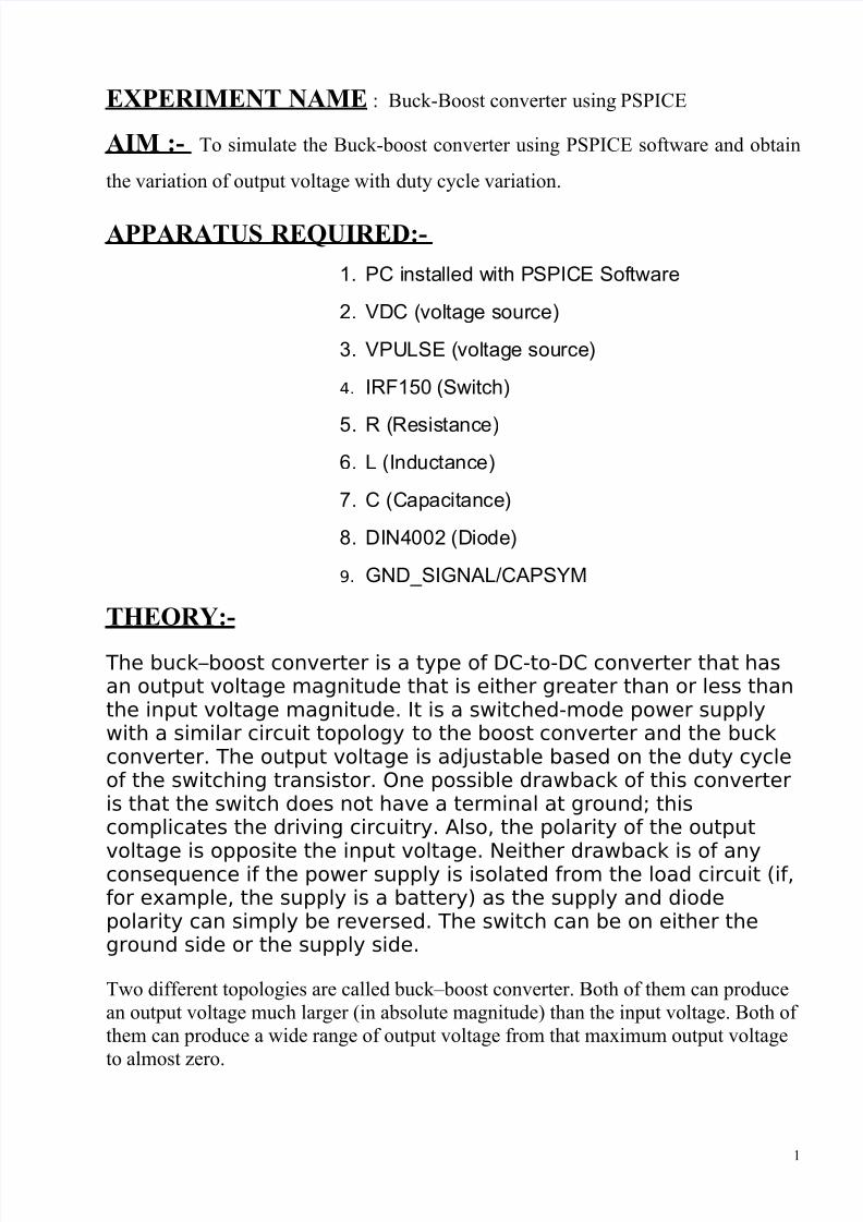
• while switch is in the On-state, the input voltage source is directly connected to
the inductor (L). This results in accumulating energy in L. In this stage, the
capacitor supplies energy to the output load.
• while switch is in the Off-state, the inductor is connected to the output load and
capacitor, so energy is transferred from L to C and R.
Compared to the buck and boost converters, the characteristics of the buck–boostconverter are mainly:
• polarity of the output voltage is opposite to that of the input;
• The output voltage can vary continuously from 0 to (for an ideal converter).
The output voltage ranges for a buck and a boost converter are respectively 0
to and to
• in continuous mode, ;
CIRCUIT DIAGRAM:-
2
8/2/2019 8.Buck Boost Converter
http://slidepdf.com/reader/full/8buck-boost-converter 3/5
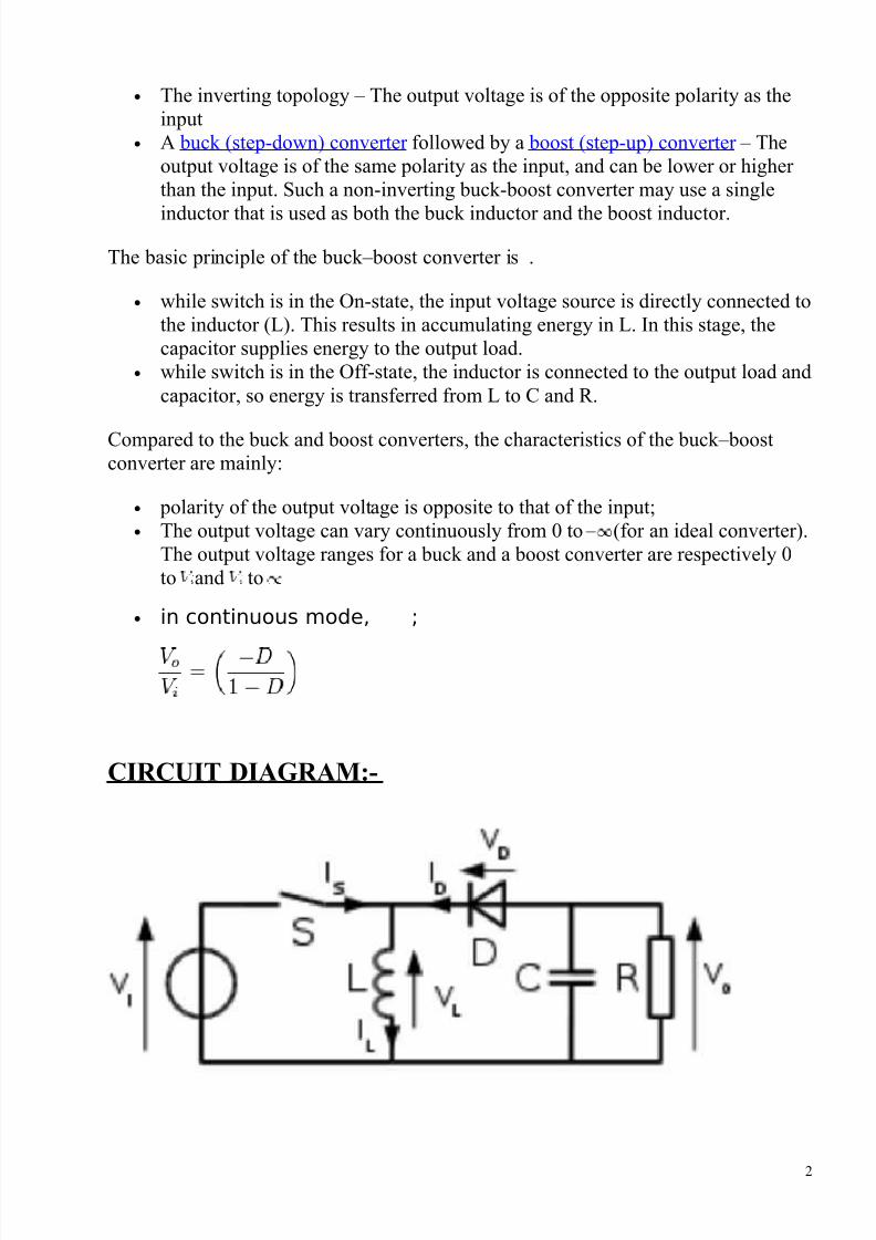
Waveforms of current and voltage in a buck–boost converteroperating in continuous mode.
PSPICE Simulation Diagram :
L 1
4 0 u H
1
2
d u t y c y c l e = P W / P E R
f s w i t c h = 5 0 k h z
r i p p l e = 0 . 0 1
i n d u c t a n c e = { ( 1 - d u t y c y c l e ) * r e s
c a p a c i t a n c e =
{ ( 1 - d u t y c y c l e ) / ( 8 * i n d u c t a n c e * r i
D 1
D 1 N 4 0 0 2
R 1
1 0
C 1
5 0 u
0
V 2
1 2 V d c
M 2I R F 1 5 0
V 1
T D = 1 u s
T F = 1 u s
P W = . 0 1 2 m s
P E R = . 0 2 m s
V 1 = 0
T R = 1 u s
V 2 = 1 0
3
8/2/2019 8.Buck Boost Converter
http://slidepdf.com/reader/full/8buck-boost-converter 4/5
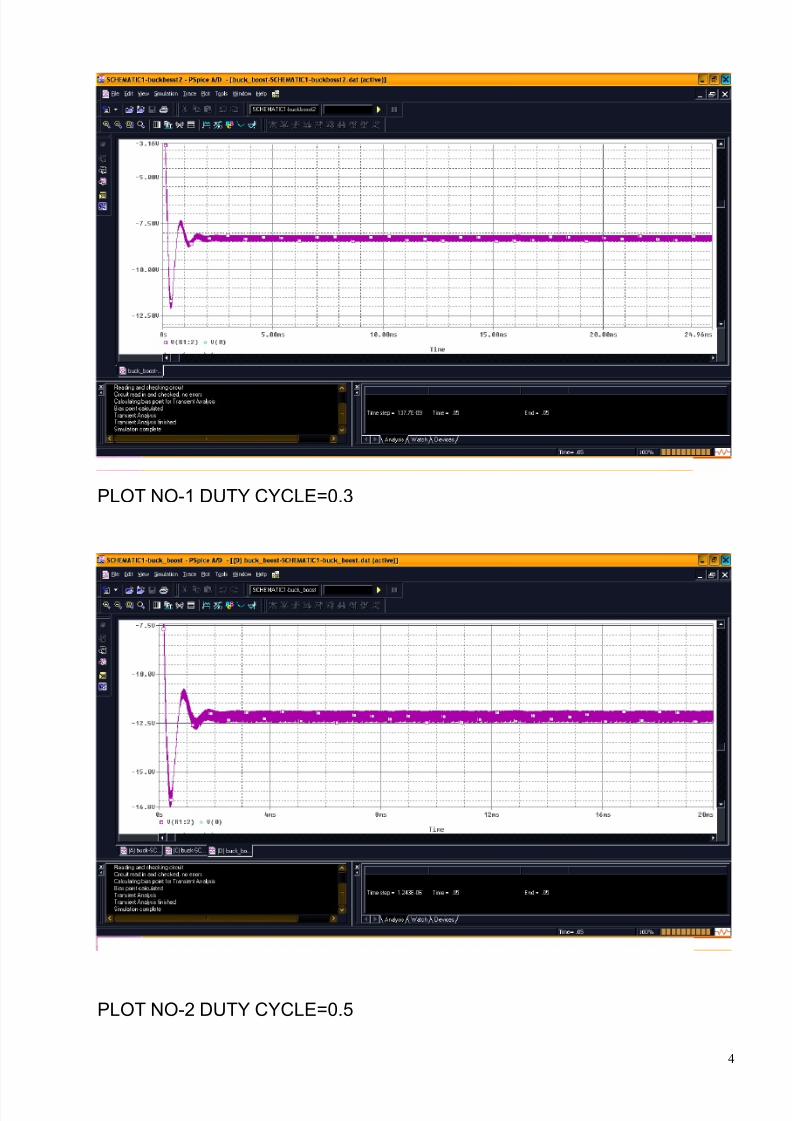
PLOT NO-1 DUTY CYCLE=0.3
PLOT NO-2 DUTY CYCLE=0.5
4
8/2/2019 8.Buck Boost Converter
http://slidepdf.com/reader/full/8buck-boost-converter 5/5
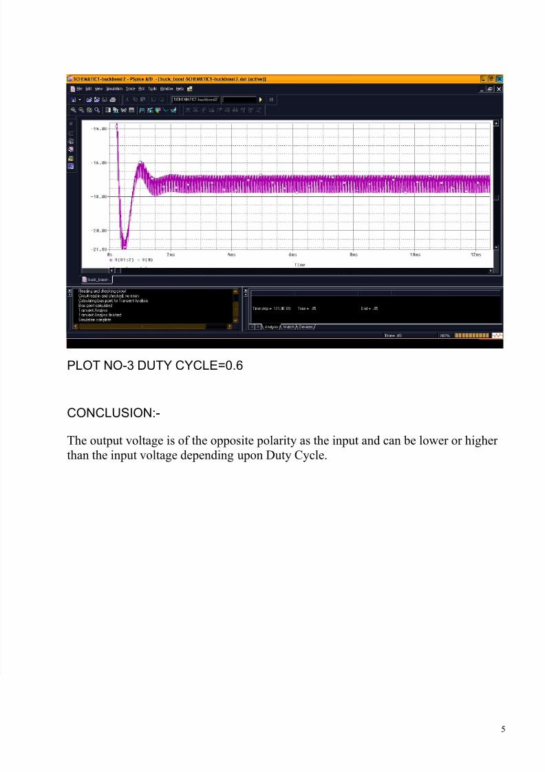
PLOT NO-3 DUTY CYCLE=0.6
CONCLUSION:-
The output voltage is of the opposite polarity as the input and can be lower or higher
than the input voltage depending upon Duty Cycle.
5
Related Documents