HAL Id: hal-03044096https://hal.archives-ouvertes.fr/hal-03044096
Submitted on 1 Feb 2022
HAL is a multi-disciplinary open accessarchive for the deposit and dissemination of sci-entific research documents, whether they are pub-lished or not. The documents may come fromteaching and research institutions in France orabroad, or from public or private research centers.
L’archive ouverte pluridisciplinaire HAL, estdestinée au dépôt et à la diffusion de documentsscientifiques de niveau recherche, publiés ou non,émanant des établissements d’enseignement et derecherche français ou étrangers, des laboratoirespublics ou privés.
Charge transport in high-mobility conjugated polymersand molecular semiconductors
Simone Fratini, Mark Nikolka, Alberto Salleo, Guillaume Schweicher, HenningSirringhaus
To cite this version:Simone Fratini, Mark Nikolka, Alberto Salleo, Guillaume Schweicher, Henning Sirringhaus. Chargetransport in high-mobility conjugated polymers and molecular semiconductors. Nature Materials,Nature Publishing Group, 2020, 19 (5), pp.491-502. �10.1038/s41563-020-0647-2�. �hal-03044096�
1
Charge transport in high-mobility conjugated polymers and molecular semiconductors
Simone Fratini1, Mark Nikolka2, Alberto Salleo3, Guillaume Schweicher2, Henning Sirringhaus2
1 Institute Neel, CNRS, 25 rue des Martyrs BP 166, 38042 Grenoble cedex 9, France
2 Cavendish Laboratory, University of Cambridge, Thomson Avenue, Cambridge CB30HE, UK
3 Department of Materials Science and Engineering, Stanford University, 496 Lomita Mall, Suite 102
Stanford, CA 94305-4034, USA
Abstract
Conjugated polymers and molecular semiconductors are emerging as a viable
semiconductor technology in industries such as displays, electronics, renewable energy, sensing and
healthcare. A key enabling factor has been significant scientific progress in improving their
charge transport properties and carrier mobilities, which has been made possible by better
understanding of the molecular structure-property relationships and the underpinning charge
transport physics. Here we aim to present a coherent review of how we understand charge
transport in these high mobility van-der Waals bonded semiconductors. Specific questions of interest
include estimates for intrinsic limits to the carrier mobilities that might ultimately be achievable, a
discussion of the coupling between charge and structural dynamics, the importance of molecular
conformations and meso-scale structural features, how the transport physics of conjugated polymers
and small molecule semiconductors are related and how the incorporation of counterions in doped
films, as used for example in bioelectronics and thermoelectric devices, affects the electronic structure
and charge transport properties.
2
Introduction
Organic semiconductors (OSCs) are exotic, carbon-based optoelectronic materials that owe their
unique solid-state physical properties to the soft, van der Waals bonding between individual
molecules. The π-conjugated electronic states tend to be robustly delocalised across the individual,
covalently bonded molecular units; yet, their shape depends strongly on the molecular geometry, and
the ability of the electronic wavefunctions to delocalize across molecular units is very sensitive to the
intermolecular packing. Concomitantly, the molecular units are large and may contain hundreds of
atoms, leading to complex structural dynamics with many different vibrational modes. Some of the
intermolecular and torsional modes are very soft with excitation energies down to a few 100 µeVs
resulting in large vibrational amplitudes at room temperature. This implies a strong coupling between
the electronic and structural dynamics that gives rise to unique and fascinating phenomena in these
molecular solids, such as a transient localisation of the electronic states, but is also a performance
limiting factor for their charge transport and optoelectronic properties, such as carrier mobilities or
excited state lifetimes.
Their soft molecular nature has allowed OSCs to carve out a space as an established and emerging
optoelectronic technology across a wide range of applications: Organic light-emitting diode (OLED)
display technology, which became a $25 billion industry in 2018, makes use of the near-unity
fluorescence and electroluminescence quantum yields that are now achievable in highly engineered
molecular emitters. Flexible OLED displays, which are currently being launched by several major
display manufacturers, are enabled by the robust mechanical properties of OSCs under repeated
mechanical strain and bending. OSCs can be deposited by low-cost, solution- or vacuum-based
coating or direct-write printing techniques uniformly over large areas and with low defect densities at
low process temperature (< 100°C). This is being exploited in flexible electronic applications, such as
the active matrix addressing of liquid crystal displays by organic field-effect transistors (OFETs)1.
OFETs are currently the only thin-film transistor (TFT) technology which is compatible with direct
manufacturing on low-cost plastic substrates, such as polyethylene terephthalate (PET) or triacethyl
cellulose (TAC), that do not tolerate process temperatures > 100°C. The absence of rare or toxic
3
elements in the composition of OSCs is also attractive, particularly for applications in organic
photovoltaics (OPV), which have recently made impressive advances. The unique ability of OSCs to
combine mixed electronic and ionic conduction is enabling emerging applications in organic
electrochemical transistors (OECTs)2, chemical and biological sensors, thermoelectrics3 as well as
neuromorphic devices for machine learning4. In the future it might become possible to combine all
these attributes to realize stretchable optoelectronic systems interfaced directly with soft biological
systems for personal health monitoring or drug delivery5.
This review is focused on the charge transport properties of OSCs. The charge carrier mobility of
OSCs, which is one of the main performance metrics for OFETs but also crucially impacts all other
device applications, has improved from the very low values of 10-6 - 10-5 cm2/Vs of the first OFETs
demonstrated in the late 1980’s to values > 1-10 cm2/Vs. There is an important debate about the most
reliable methods for extracting mobility values from the characteristics of OFETs and not all high
mobility values claimed in the literature can be considered reliable6,7. However, there is clear evidence
that the mobility of the best organic semiconductors now exceeds that of thin films of amorphous
silicon. This impressive advance in performance has been enabled by a broad exploration of
molecular structures by organic chemistry, a detailed understanding of the underpinning structure-
property relationships, an optimisation of all aspects of device architecture and the elimination of
extrinsic, transport-limiting impurities; these subjects have been the focus of several excellent
reviews8,9. Importantly, the search for better materials has been guided both by an increasingly
sophisticated understanding of the microscopic charge transport physics on the molecular scale, and
by an increasing appreciation of the role of transport processes occurring at larger length-scales. In
recent years the transport physics of a number of high mobility small molecule as well as conjugated
polymer model systems has been investigated in great depth and it has been possible to unravel the
complex factors that determine the charge carrier mobilities of these materials. The focus of the
present review is to discuss these recent advances in physical understanding, in particular of the
relationship between structural disorder and dynamics and charge transport properties in both small
molecule and conjugated polymer systems. It also aims to identify directions for future research that
4
might enable OSCs to reach ultimate mobility limits for such van der Waals bonded materials. The
case of systems containing ions, relevant for applications such as OECTs and thermoelectrics, will
also be discussed briefly, highlighting how the electronic structure of OSCs is modified and how high
carrier mobilities can be maintained.
Transport physics of crystalline molecular semiconductors
Charge transport properties of molecular semiconductors are directly related to their molecular
structure and assembly in the solid-state (their crystal structure). Although molecular structure plays
an important role, it is the packing of individual moieties within the solid-state that determines the
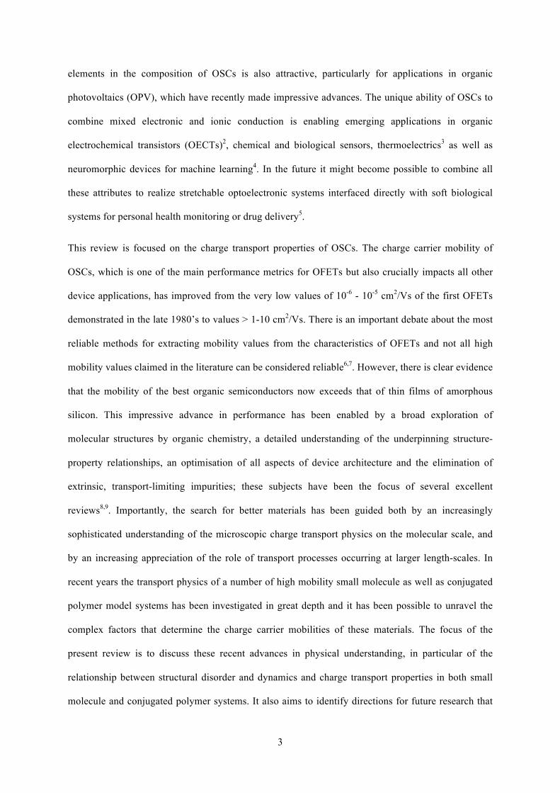
overlap of neighbouring orbitals and defines pathways for charge transport. A top view of the four
mostly commonly observed packing motifs with an indication of the dominant transfer integrals (J)
between adjacent molecules is presented in Figure 1, together with relevant examples of prototypical
molecular structures. Transport takes place primarily within the x-y plane. Systems that offer only one
large J exhibit strongly anisotropic transport with carrier mobilities being highest in one specific
direction. This is commonly found in slipped-stack (Figure 1a) or slipped π-stack (Figure 1b)
configurations that are distinguished by the molecular orientation in adjacent columns being the same
or rotated. The anisotropy of transport can easily be tuned with molecular packing: for herringbone
packing there are three large transfer integrals (Figure 1d); this can provide isotropic transport
properties in the x-y plane when the three values of J are equal or very similar.10,11 Brick-wall packing
in which there tends to be only two large transfer integrals may be consider an intermediate regime
(Figure 1c). With the exception of rubrene, which remains the molecule with the highest reproducible
mobility so far (> 15 cm2 V-1 s-1) in a slipped π-stack packing, charge carrier mobilities are commonly
found to be highest in systems with isotropic distribution of transfer integrals12,13; we discuss the
associated physics in more detail below (Table 1). A brief overview over some of the highest mobility
molecular semiconductors discovered to date and their structure property-relationships is given in Box
1.
Detailed experimental charge transport investigations have been undertaken on several high mobility
model systems and have given insight into the magnitude of the key parameters that govern charge
5
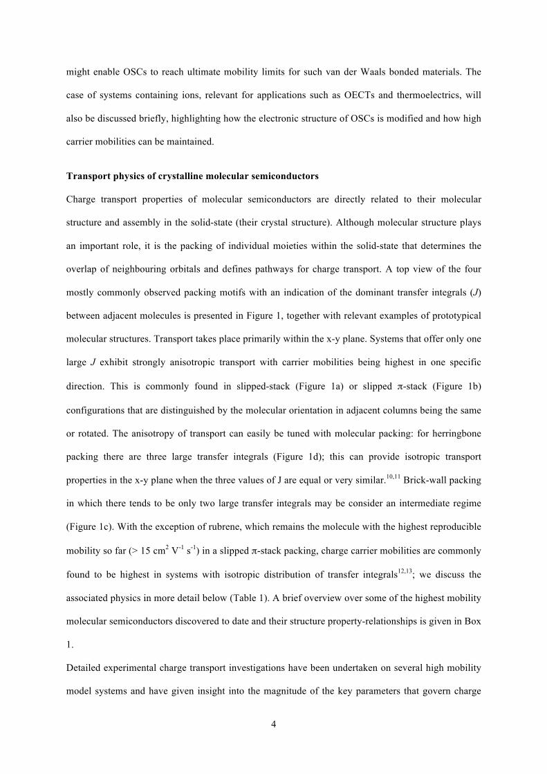
transport. Angle-resolved ultraviolet photoemission spectroscopy (ARUPS) experiments have yielded
quantitative values of the transfer integrals and confirmed that these are on the order of 100 meV as
predicted by band structure calculations.14 These measurements also provided direct evidence for
temperature-dependent hole-phonon coupling in the observed band dispersion15 consistent with
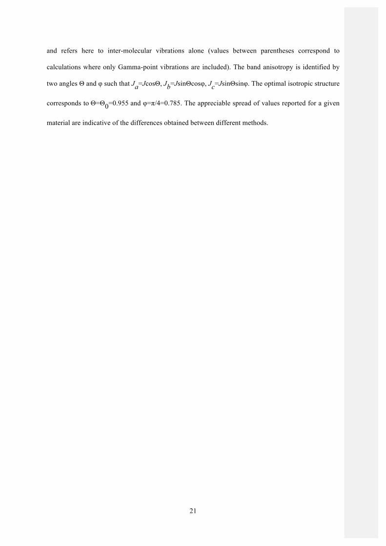
theoretical predictions (Figure 2a) 16,17 A careful analysis of diffuse scattering features in transmission
electron diffraction has allowed a direct experimental determination of the amplitude of thermal
lattice fluctuations, which were found to be on the order of 0.1-0.2 Å at room temperature in several,
widely studied molecular crystals. Such large amplitudes reflect the soft, non-covalent bonding
between molecules and imply that there must be corresponding temporal fluctuations in the transfer
integrals between adjacent molecules on the order of a 10-20% on the picosecond timescale on which
these vibrations occur 18,19. This suggests that non-diagonal, dynamic disorder in the transfer integrals
must be an important factor in the transport physics of these molecular crystals.
Charge carriers in crystalline inorganic semiconductors, such as Si, are Bloch electrons with
delocalized wavefunctions extended over the crystalline lattice. Some of the transport signatures
commonly observed in molecular crystals are reminiscent of transport in inorganic semiconductors,
including the ideal Hall signature already discussed and what is commonly referred to as a band-like
temperature dependence of the mobility, for which the mobility increases with decreasing temperature
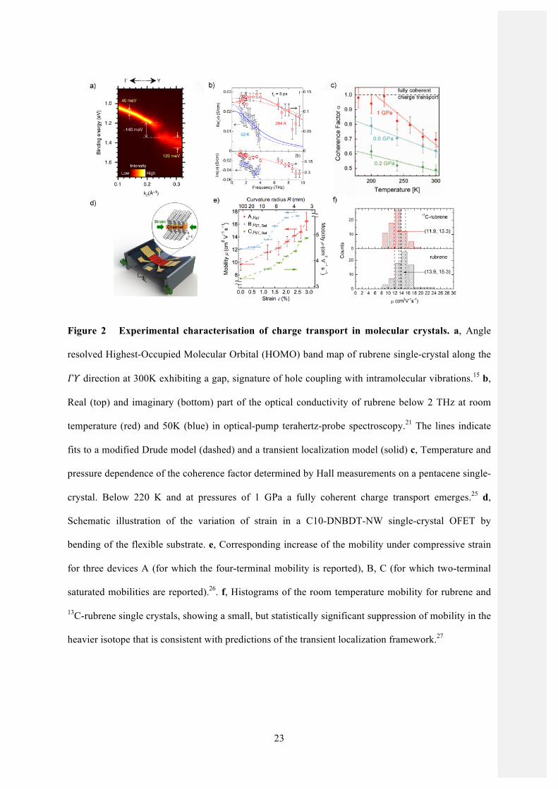
in the limited temperature range between typically 150K and room temperature (Figure 3c).20
However, in molecular crystals optical spectroscopy, which probes the electronic states of the carriers
on timescales faster than those of lattice vibrations, has provided direct evidence that charge carriers
in molecular semiconductors are in fact not spatially fully extended Bloch electrons: at infrared
frequencies charge carriers in rubrene molecular crystals exhibit a deviation from a simple Drude-like
free carrier response that manifests itself in a suppression of the optical conductivity below 2THz near
room temperature and is a characteristic signature of the transient localisation physics discussed
below (Figure 2b).21–23 In charge modulation spectroscopy experiments with optical frequencies, the
charge-induced absorptions have a clear molecular character and resemble those of radical
6
cations/anions in solution, suggesting that on ultrafast timescales the electron wavefunction is
delocalized at best over small clusters of molecules.24
Several recent transport studies have been able to correlate a suppression of thermal lattice
fluctuations with enhancement of carrier mobility and coherence of charge transport: By applying
hydrostatic pressures up to 1GPa at low temperatures thermal disorder was significantly reduced and
an ideal Hall signature was induced in single-crystal pentacene FETs25, which cannot be observed at
room temperature and ambient pressure in this system (Figure 2c). Similarly, an increase of the field-
effect mobility of C10-DNBDT-NW single-crystalline films from 9 to 16 cm2/Vs was observed under
compressive strain of up to 3% (Figure 2e), which is too large to be explained by simple strain-
induced changes expected within a Bloch electron band structure framework, but is quantitatively
consistent with the reduction in dynamic disorder expected for the strain-induced stiffening of the
molecular lattice26. A strong isotope effect was shown in rubrene single crystals (Figure 2f)27, that is
not expected in a band transport regime dominated by acoustic phonon scattering, but is consistent
with the expected increase of carrier localisation due to increased vibrational amplitude upon C13-
substitution.
To rationalize these unusual transport signatures within a consistent theoretical framework it is helpful
to consider the description of the motion of Bloch electrons in conventional conductors and
semiconductors as a succession of individual collisions with scattering centers — static defects and
dynamical lattice vibrations — in an otherwise perfectly crystalline arrangement. Such semi-classical
"band" picture holds provided that the mean free path between collisions is much larger than the
lattice spacing or, equivalently, when the semiclassical scattering rate 1/τ is much smaller than the
electronic transfer rate J/ħ between lattice sites 28,29. Assuming the Drude formula µ=eτ/m*, where the
band mass m*∼ħ2/(2Ja2) , with a≃6Å a typical inter-molecular distance, and setting the
phenomenological condition (ħ/τ)/J = 0.25 yields approximately µ ≳ 50 cm2/Vs as a lower bound for
the applicability of Bloch-Boltzmann (band) transport. 30
7
As discussed above high-mobility organic semiconductors display room-temperature mobilities in the
range µ ≈ 1−20 cm2/Vs, well below this band limit. In this class of materials, the thermal vibrations
of the constituent molecules are so large that they enable quantum microscopic processes beyond the
semiclassical description: in the presence of strong molecular disorder, the electronic wavefunctions
show a marked tendency to localisation at short times, ≲1ps, leading to a sizeable suppression of the
charge diffusivity 31,32. This physical mechanism, which has been denoted transient localisation (TL),
translates into a mobility of the form:29
𝜇 = !!!!
!!
!!!"# (1)
This formula shows explicitly that the parameters governing charge transport in this regime — the
transient localisation length L and the timescale 𝜏!"# of inter-molecular motions — differ from those
relevant in conventional semiconductors — the effective mass m* and scattering time τ. The transient
localisation mechanism is able to reconcile the observation of "band-like" mobilities which decrease
with temperature, yet with absolute values that (precisely due to the presence of localisation processes
slowing down the carrier motion) fall below the range of band transport. Figure 3a illustrates the
charge carrier wavefunction and transport mechanism in the TL regime ; for a realistic visualisation
on an actual molecular system see Ref. 33, which also provides a recent validation of the TL scenario
by an independent theoretical method.
When disorder is so strong that the carriers become localised on a single molecular site, Eq. (1) ceases
to be valid and a transition to a thermally activated hopping regime is expected.34–37 The breakdown of
the TL regime can be estimated by setting L≃a in Eq. (1): taking kBT≃25meV and 𝜏!"# = 𝜔!!!, with
ħω0≃5meV in the typical range of the inter-molecular vibration frequencies in molecular crystals,
yields µ ≲ 0.5 cm2/Vs.
The knowledge gained from Eq. (1) provides important predictions and general guidelines to improve
the transport characteristics of materials: to achieve the highest carrier mobilities within the transient
localisation regime one should aim at minimising localisation effects, in order to increase the transient
8
localisation length L as much as possible. This can be achieved by acting principally on two factors.
The first is the energetic disorder σ, which is unavoidable even in perfectly crystalline systems, and
mostly originates from the thermal fluctuations of the inter-molecular transfer integrals31,38,39. The
mobility decreases with dynamical disorder as a power law, µ∝(σ/J)−ν, with J setting the scale of the
electronic bandwidth and ν a material-dependent exponent that has been calculated to be in the range
1.5<ν<3.530. While the presence of thermal molecular disorder is tied to the very nature of weakly
bonded molecular solids, the large variability of ratios σ/J observed across different compounds
(Table Erreur ! Source du renvoi introuvable.) shows that there is ample room for optimising this
parameter, and hence the mobility, via a proper engineering of inter-molecular interactions. In
principle, this can be achieved either by suppressing the absolute disorder 𝜎, or by increasing 𝐽 at
fixed disorder. In this respect, it has been shown recently that combining experimental spectral probes
together with a theoretical analysis of the individual vibrational modes can provide key information to
understand and control molecular disorder at the microscopic level40. There is evidence that the
thermal disorder is dominated by few, in some systems just a single vibrational, ‘killer’ modes39. If
these modes could be targeted by molecular design and their contribution to thermal disorder be
reduced, this could result in significant improvements in performance. According to the scaling form
given above, reducing the disorder ratio σ/J from 0.5 to 0.3 can result in an improvement of µ by up to
a factor 6. Of similar importance are also the dynamic fluctuations of the diagonal electron-phonon
coupling and the site energies30,39,41.
The second important parameter governing charge transport is the degree of anisotropy of the band
structure. This is determined by the relative values of the transfer integrals in the different bond
directions (Figure 1), which ultimately control the sensitivity of carrier motion to disorder38. It has
been shown that, to optimize the transport of hole carriers, one should aim at structures with inter-
molecular transfer integrals that are isotropic in the different directions and for which the product of
signs of the different transfer integrals is positive, as these are the most resilient to quantum
localisation effects38. This has been recently shown for systems with three dominant transfer integrals,
in which the distribution of transfer integrals can be represented as a point on a sphere, but is likely to
Simone Fratini� 17/2/20 14:49Supprimé: 1
9
remain valid as well for systems with more complex band parameters38. Without acting on the amount
of disorder itself, the mobility of an organic semiconductor in the most conducting direction can
increase by up to a factor of 6 when going from a purely one-dimensional to such an ideal isotropic
two-dimensional structure, and possibly more in three dimensional structures.
Stiffening the inter-molecular bonds via strain or chemical functionalisation has been proposed as a
possible strategy to improve charge transport 19,26,29,42, as this reduces the molecular fluctuation time
𝜏!"# = 𝜔!!!, which appears explicitly in Eq. (1). However, the expected changes in mobility are weak
29,38, and the outcome is likely dominated by concomitant modifications of σ/J 41 and of the band
structure anisotropy39. Finally, the mobility increases with the inter-molecular distance as µ∝a2,
which follows from basic dimensional arguments. This effect has been suggested to contribute to the
outstanding performances of rubrene, where the inter-molecular distance in the direction of highest
mobility is exceptionally large due to the slipped-stack structure39. Of course it is also important to
consider that the electronic couplings decay exponentially with distance, which means that a large
lattice spacing may not be beneficial in all systems.
It is interesting to contrast these conclusions43, that apply within the transient localisation regime, with
the band transport predictions. The band mobility can be written in full generality as
𝜇 = 𝜇 𝜆 𝐽 𝑘!𝑇 ! , with λ a dimensionless electron-phonon coupling strength and 𝜇 = 𝑒𝑎! ℏ
carrying the mobility units. The exponent p was calculated within a model system approach 38 and
was found to be material dependent, ranging in the interval 0.5<p<1.2 when only inter-molecular
fluctuations are considered, whereas a higher exponent p≃2.6 was reported from a fully ab-initio
calculation in naphthalene44. Unlike the TL result, the band mobility within the thermal regime
relevant to organic semiconductors, kBT≳ħω0/2, is independent of ω0. The dependence on energetic
disorder can be obtained from the above expression by substituting the definition 𝜎 ∝ 𝜆𝐽𝑘!𝑇 29,30,38,
which yields µ∝(σ/J)−2 . The dependence of µ on the band structure anisotropy resembles
qualitatively that reported for the TL regime, with optimal values reached for isotropic band
structures38.
10
Paralleling the current experimental efforts in exploring novel molecular compounds 10,19,26,40,45,46
theoretical estimates of the relevant disorder and band parameters are also becoming available. Table
Erreur ! Source du renvoi introuvable. summarises such parameters for a number of materials of
current interest. It is remarkable that while low levels of disorder, σ/J ≲ 0.3, and nearly ideal band
structures have been independently achieved in current materials (highlighted in bold), no compound
exists yet that is able to combine such optimal features together. If such a compound could be
synthesized, mobilities surpassing those of the best molecular semiconductors discovered to date,
including rubrene (µ ≃ 15cm2/Vs) could be achieved. Assuming that localisation effects are
minimised in such an ideal compound, we can use Bloch-Boltzmann theory which predicts
𝜇 = 0.81 𝜇 𝜎 𝐽 ! for an isotropic material with J=100 meV at room temperature. Substituting
σ/J=0.3 in this expression with 𝜇 ≃ 6cm2/Vs for a=6Å yields µ≃50 cm2/Vs, at the onset of the band
transport regime. This value, which has been obtained by considering only the effects of inter-
molecular disorder, should be considered as an ideal upper bound for actual materials and devices.
Of course reaching such mobility limits in any new material will require elimination of any static
structural defects, such as point defects or grain boundaries. We have not elaborated on such extrinsic
issues in this review, which can be very important in specific systems.47 In this review we have
focussed on molecular systems believed to be limited instead by intrinsic TL factors. Turning now to
polymers, such static structural disorder effects move centre-stage and any attempt to understand
charge transport in polymers must start with detailed studies of their complex microstructure.
Charge transport in low-disorder conjugated polymers
Research on high-mobility conjugated polymers in recent years has moved away from the simple
polythiophene conjugated polymers that dominated the field 20 years ago and is focussed largely on
more rigid, fused-ring polymers - in particular donor-acceptor (D-A) copolymers with alternating
electron-rich and electron-deficient units along the backbone of the polymer. Several excellent
reviews have discussed the molecular design and structure-property relationships of these D-A
copolymers48,49,9; we present a brief overview over some of the most widely studied, high mobility
Simone Fratini� 17/2/20 14:49Supprimé: 1
11
systems in Box 1. Achieving higher carrier mobilities is usually favoured by higher-molecular
weights50 although mobility improvements with molecular weight tend to tail off for values above 100
kDa51. This reflects the need for chains to be long enough so they can act as tie-chains to interconnect
between adjacent crystalline domains. Uniaxial alignment of the polymer chains during the deposition
process generally leads to higher mobilities along the chain alignment direction. In
diketopyrrolopyrrole-benzothiadiazole (DPP-BTz) and CDT-BTz, the alignment of polymer chains
has resulted in field-effect mobilities that can reliably achieve 7 and 10 cm2/Vs52,53, respectively.
Similar enhancement of mobility from 1 cm2/Vs for unaligned films to 5 cm2/Vs in the direction of
chain alignment has also been observed in n-type poly(bis(octyldodecyl)naphthalene-
bis(dicarboximide)-diyl]-alt-bithiophene) (P(NDI2OD-T2)54. An important feature in all these highest
performing polymers is a degree of energetic disorder that is on the order of ~kBT 55,56,57. The
energetic disorder can be quantified, for example, by determining the Urbach energy, which is a
measure of the width of the tail of the optical absorption near the band gap. It is remarkable that many
high mobility D-A copolymers, which have poorer crystallinity than P3HT/PBTTT, exhibit in fact
significantly lower energetic disorder. This is believed to reflect more uniform distribution of
conformations of the polymer backbone throughout the films55.
Despite the high mobility values that in some cases are close to those of the molecular crystals
discussed above, the temperature dependence of the field-effect mobility in most polymer systems is
found to be thermally activated (Figure 3d). This is usually interpreted as a manifestation of residual,
essentially static energetic disorder in the density of states due to spatial variations in the
conformation of the polymer chain segments that charges encounter as they hop through the network
of chains. In a few systems such as diketopyrrolopyrrole-triethylene glycol (2DPP-TEG), CDT-BTz
as well as aligned diketopyrrolopyrrole-benzotriazole (DPP-BTz) a transition from a thermally
activated behaviour at low temperatures to a “band-like” temperature dependence near room
temperature has been observed52,53,58,59. However, this observation by itself should not be considered
conclusive evidence for a band or TL charge transport regime. The most convincing evidence to date
that such a regime can in fact be reached in a polymer system stems from studies on aligned CDT-
12
BTz, where a band-like signature in the temperature dependence of the mobility along the chain
alignment direction was observed together with a clear Hall effect, suggesting that at least some of the
charge carriers are sufficiently delocalized to couple to a magnetic field (Figure 4a).52,59
The favourable transport properties of low-disorder polymers also extend to the bulk as probed in
diode structures, where much lower carrier densities prevail than at the interfaces of an FET. Some D-
A copolymers, such as DPP-BTz and as well as (P(NDI2OD-T2)), have shown among the highest
bulk carrier mobility in single carrier diodes with space charge limited current mobilities approaching
those measured in FETs60,61. Here, the impact of lower energetic disorder directly translates into a
faster filling of tail states in the density of states (DOS) and thus significantly improved
performances61. In OLEDs and OPV device performance is of course governed by multiple, complex
factors, not just charge transport, but the high bulk charge carrier mobility tends to increase current
density and reduce power consumption and the low degree of energetic disorder enables larger quasi-
Fermi level splitting and higher open circuit voltages.62.
When aiming to understand charge transport in conjugated polymers it is important to consider
processes across multiple length-scales. Indeed, it has been shown both theoretically and
experimentally that carrier mobility in polymers exhibits a marked time dependence (Figure 4b) 63,64.
Length-scales map onto timescales, therefore different factors play a role in governing mobility,
depending on the process of interest (Figure 4c). This is relevant not just for understanding charge
transport, but also for other processes, such as operation of OPV: For instance, on-chain, short-
timescale transport is important for charge generation at the donor-acceptor interface, where charges
must move only a few nanometers away from each other to avoid recombining. Yet the charge
collection process relies on transport processes with much longer characteristic timescales as charges
cross tens to hundreds of nanometers in order to reach the current contacts.
At the molecular scale, charges must be able to delocalize and move along the chains. Eventually,
however, charges will have to move from chain to chain due to the occurrence of chain ends or kinks
that act as structural traps. Local transport along single chains, corresponding to short times (<~10
ps), albeit challenging to measure accurately, has been estimated using THz pump-probe, time-
13
resolved electric-field induced second-harmonic generation, and pulse radiolysis time-resolved
microwave conductivity. 63,65 As intuitively expected, on-chain mobility is orders of magnitude larger
than that measured over macroscopic distances by characterizing electronic devices. For instance, on-
chain mobilities as high as 600 cm2/Vs have been measured in ladder-type polymers66.
The mesoscale (10-100 nm) arrangement of transport paths plays an important role in governing
mobility as well. In semicrystalline microstructures, due to the longer conjugation length and
increased intermolecular coupling in ordered regions compared to the amorphous polymer, charges
tend to be confined to the ordered regions67,68. Thus, charges experience an injection barrier as they
cross from the crystallites into the amorphous intercrystallite regions. This barrier into amorphous
regions would slow down transport; moreover, transport in amorphous microstructures is inherently
slower than in crystallites. Traversing amorphous regions is therefore very detrimental to transport.
Crystallites are considered effectively electrically connected when they are bridged by a relatively
straight tie-chain, which requires the distance between crystallites to be not much longer than the
polymer persistence length69. Under these conditions, charges can effectively travel from crystal to
crystal without experiencing significant impediments due to the amorphous intercrystallite regions.
The importance of tie-chains was recently confirmed in studies involving blends of polythiophene
batches having different molecular weights70. It was shown that, when the fraction of tie-chains
exceeds ~10-4, transport becomes more efficient independently of the details of the chain lengths and
distributions in the polymer (Figure 4d). This observation suggests an interesting parallel between
electrical and mechanical properties of semicrystalline polymers, where for instance the Huang-
Brown model uses the fraction of tie-chains to interpret the microstructural origins of some
mechanical properties of polyolefin resins.
At larger length-scales (hundred of nanometers to microns) high mobility in semicrystalline
microstructures is obtained when charges can travel from crystal to crystal without entanglements or
abrupt changes in the polymer backbone direction. As a result, polymers that have rigid chains -
giving rise to gradual, low-angle grain-boundaries where transport paths with no abrupt backbone
direction change can exist - would exhibit more favorable transport properties 71. Indeed, it has been
14
shown that semicrystalline polythiophene films having undergone an alignment process whereby both
low angle and high angle grain boundaries coexist, consistently exhibit a higher mobility only in the
direction of the low-angle grain-boundaries72. A possible exception to this observation has been
hypothesized for certain rigid molecules that display pseudo-epitaxial relationships between crystals
called quadrites73. Quadrites may provide facile transport paths even between crystals having large
misorientations, provided these are special angles dictated by the molecular structure of the polymer74.
Quantitative insight into these complex transport processes in polymers over multiple length scales
can be derived from multi-scale theoretical simulations. These typically involve the steps of
simulating realistic morphologies by molecular dynamics, partitioning into conjugation segments,
calculating molecular charge transfer rates for pairs of conjugation segments and simulating the
charge dynamics by Master Equation / kinetic Monte Carlo methods75,76. These methods were first
applied to molecular systems such as discotic liquid crystals77, but have since also been shown to
provide realistic estimates of carrier mobilities in conjugated polymers, including P3HT78, PBTTT79,80
or the D-A copolymer PCPDTBT81. For PBTTT it was shown that the fluctuations in the transfer
integrals (that is dynamic disorder) occur mostly on timescales of <100 fs that are faster than the
timescale for charge transfer. This implies that charge transfer may be considered to be governed by
an average value of transfer integral. On the other hand the evolution of the landscape of energetic
disorder occurs mostly on slower time scales: most hopping steps can be considered to occur within a
static landscape of energetic disorder79. Only for the slowest hopping processes involving trap states
can the energetic landscape be considered self-healing, i.e. charges can escape these trap sites as a
result of conformational reorganization on a time scale of 0.1ns80. Approaches based on model
Hamiltonians have also provided powerful insight into the key processes and factors that govern
charge transport in high mobility polymer systems, such as how dynamic disorder mediates the
hopping between states defined by static disorder82, the influence of bandwidth in D-A copolymers on
carrier mobility 83, and the identification of the most important parameters governing mobilities84. A
particularly important insight has been the realization of the significance of delocalized states that are
15
available at energies < kBT away from the band edges and can mediate hopping processes over long
distances82.
Conjugated polymers are generally more challenging to understand than molecular crystals due to
their inherently disordered nature. Strategies for improving carrier mobilities often focus on making
polymers resilient to disorder by mitigating its effects. As explained above, in semicrystalline systems
this is achieved by straight tie-chains connecting crystallites electrically through the inevitable
amorphous regions of the polymer without letting these slow down transport. In D-A copolymers such
as IDT-BT, with low degree of energetic disorder and mobilities higher than 2 cm2/Vs, that cannot be
considered semicrystalline but appear quasi-amorphous, the principle of making transport resilient to
disorder must apply even more strongly because these materials are structurally more disordered than
semicrystalline polymers. Such systems exhibit extended rigid, fused-ring conjugated units connected
by only a few torsion-susceptible single bonds that are designed to exhibit steep torsion potentials. As
a result the polymer backbone adopts a nearly planar, largely torsion-free conformation owing to its
rigidity (Figure 3d). Polymer chain conformations can be predicted theoretically from molecular
dynamics simulations, but can also be visualized for polymers adsorbed on surfaces by scanning
tunneling microscopy techniques (Figure 4e)85. In addition, the inherently smaller intrachain
bandwidth in D-A copolymers also makes transport less sensitive to conformational disorder83. As a
result the edge of the density-of-states in such D-A copolymer systems does not suffer from
significant disorder-induced broadening, meaning that the structural disorder does not induce deep
electronic traps55. One might consider a system like IDT-BT as a limiting case of a semicrystalline
system, where the crystalline domains have shrunk to very small, aggregate regions or simply close
contact points between adjacent chains86. Such close contact points remain crucial for mediating
efficient charge transport between chains. For charges in such a system to move efficiently in between
close contact points, the intrachain electronic structure must be resilient to disorder. Such insensitivity
to structural disorder should also be beneficial in semi-crystalline systems, as otherwise transport
along tie chains could limit charge transport, and may be the reason why D-A copolymers generally
exhibit higher carrier mobilities than P3HT and PBTTT.
16
It is clear from the above discussion that, despite mobilities being quantitatively similar the
descriptions of charge transport in crystalline molecular semiconductors and structurally more
disordered conjugated polymers differ significantly. In the former, mobilities reflect directly the
dynamic disorder due to intermolecular phonon modes, that lead to the TL of carriers. In contrast, in
high mobility conjugated polymers, where intrachain transport along the chains can be considered to
be fast, mobilities are limited by residual, essentially static disorder in the intermolecular packing
encountered within crystallites/aggregate regions or along the tie-chains that connect these
crystallites/aggregates. The interesting question arises to which extent there are also similarities
between molecules and polymers. In polymers there is an equivalent coupling between the charge and
structural dynamics as in molecular systems: The static energetic disorder due to conformational
variations encountered along the polymer backbone defines localized electronic states in the
individual conjugation segments (Figure 4c). The vibrational modes of the polymer chain, the high-
frequency modes - such as C-C stretch vibrations, but also the low frequency modes, such as torsional
vibrations - couple to the electronic structure and cause dynamic disorder, which is ultimately
responsible for mediating coupling between localized states on adjacent states and intrachain hopping
along the chain.82 However, while the carriers remain on a particular site, the electronic coupling to
the vibrational modes also causes fast oscillations of the carrier wavefunction along the polymer
backbone driven by the structural dynamics. These fast oscillations of the carrier wavefunction along
the backbone around the sites defined by static disorder can be directly observed in optical
spectroscopy as they lead to large enhancements of the oscillator strength for optical absorption by
infrared vibrational modes87. They are similar to the charge carrier diffusion driven by the structural
dynamics in the TL regime of molecular crystals. However, in polymers they do not directly manifest
themselves in the mobility which remains limited by slower, interchain and difficult intrachain
hopping processes. It has recently been suggested that this strong coupling between charge and
structural dynamics on ps timescales and molecular length scales, which occurs in both systems, may
be responsible for a striking similarity in the spin relaxation physics of spin-1/2 charge carriers in
molecular and polymeric systems. Despite opposite trends in the temperature dependence of the
carrier mobility the spin relaxation times in the two systems exhibit very similar magnitudes and
17
decrease with increasing temperature between 100-150K and room temperature (comparison between
Figure 3c and d)88,89.
For polymeric systems it is difficult to predict ultimate mobility limits; in principle, the fast intrachain
transport along the polymer backbone could support mobilities exceeding 100 cm2/Vs, but there are
currently no clear strategies for overcoming the limitations imposed by the slower interchain charge
transfer processes, that, even in aligned polymer films, are necessary for charges to cross practical
device dimensions. One interesting approach to overcome these limitations has been to extend the π-
conjugation to two-dimensional systems, which should be inherently less susceptible to disorder-
induced localisation. In such 2D polymers, transition metal coordination or covalent organic linkers
between conjugated units are used to synthesize extended 2D conjugated sheets. In comparison to
conventional 2D materials, such as graphene or transition metal dichalcogenides, these 2D polymers
retain a high level of chemical design flexibility and are compatible with low-temperature solution
growth. The charge transport physics of these materials is just starting to be explored 90.
Outlook
In this review we have focussed on the understanding of the charge transport physics of molecular and
polymeric semiconductors. Over the last 10 years much progress has been made in both identifying
the key molecular structure requirements for achieving high carrier mobilities and general,
experimental signatures of transport as well as building a theoretical understanding that is able to
rationalize experimentally observed differences between materials within first-principle models. Due
to their molecular nature both molecular and polymeric semiconductors exhibit a unique and
fascinating charge transport regime in which structural and charge dynamics are intimately coupled.
We hope that the level of depth of scientific understanding obtained to date will enable the discovery
of new, fundamental transport phenomena, which may not be observable in other classes of electronic
materials and could open up paths to completely new functionalities and uses. It also provides clearer
molecular design guidelines that will hopefully enable further improvements in carrier mobilities, for
which there remains significant room within fundamental limits. Based on the discussion presented in
this review promising strategies for molecular systems include the minimisation of thermal disorder
18
associated with specific vibrational modes and the simultaneous realisation of a near isotropic
distribution of transfer integrals. For polymeric systems better use needs to be made of the fast
intrachain transport along the polymer backbone in disorder-resilient polymers with long persistence
lengths. More efficient interchain transport at close crossing points might be achievable through the
incorporation of specific units into the polymer backbone that facilitate close interchain packing.
Improvements in performance are needed to meet requirements for a wider range of industrial
applications - such as flexible OLCD and OLED displays or integrated sensors and circuits for the
Internet of Things. Recently, there has been growing interest in organic semiconductors for emerging
applications in bioelectronics and thermoelectrics. For these applications it is very important to
understand the charge transport properties in a regime in which both a high concentration of ions and
electronic carriers exceeding 1018-1019 cm-3 are present throughout the bulk of the organic film. Some
of the additional and open issues of charge transport that arise in such systems are briefly highlighted
in Box 2 and we also refer to several excellent reviews on mixed electronic-ionic conduction 2,3,91. The
pursuit of such exciting application directions supported by a continued exploration of new molecular
structures and architectures suitable for these applications and an in-depth, fundamental understanding
of their charge transport physics will ensure that the field of organic semiconductors is likely to
remain vibrant.
Acknowledgements
S.F. acknowledges support by the German Research Foundation DFG (Grant No. DR228/48-1). MN
thanks the European Commission for a Marie Skłodowska-Curie fellowship. AS acknowledges
financial support from the National Science Foundation, Division of Materials Research, Award
#1808401. G.S. acknowledges postdoctoral fellowship support from The Leverhulme Trust (Early
Career Fellowship supported by the Isaac Newton Trust). HS thanks the Engineering and Physical
Sciences Research Council (EPSRC programme grant EP/M005143/1) and the European Research
Council (ERC) (Synergy grant SC2 610115) for funding.

19
20
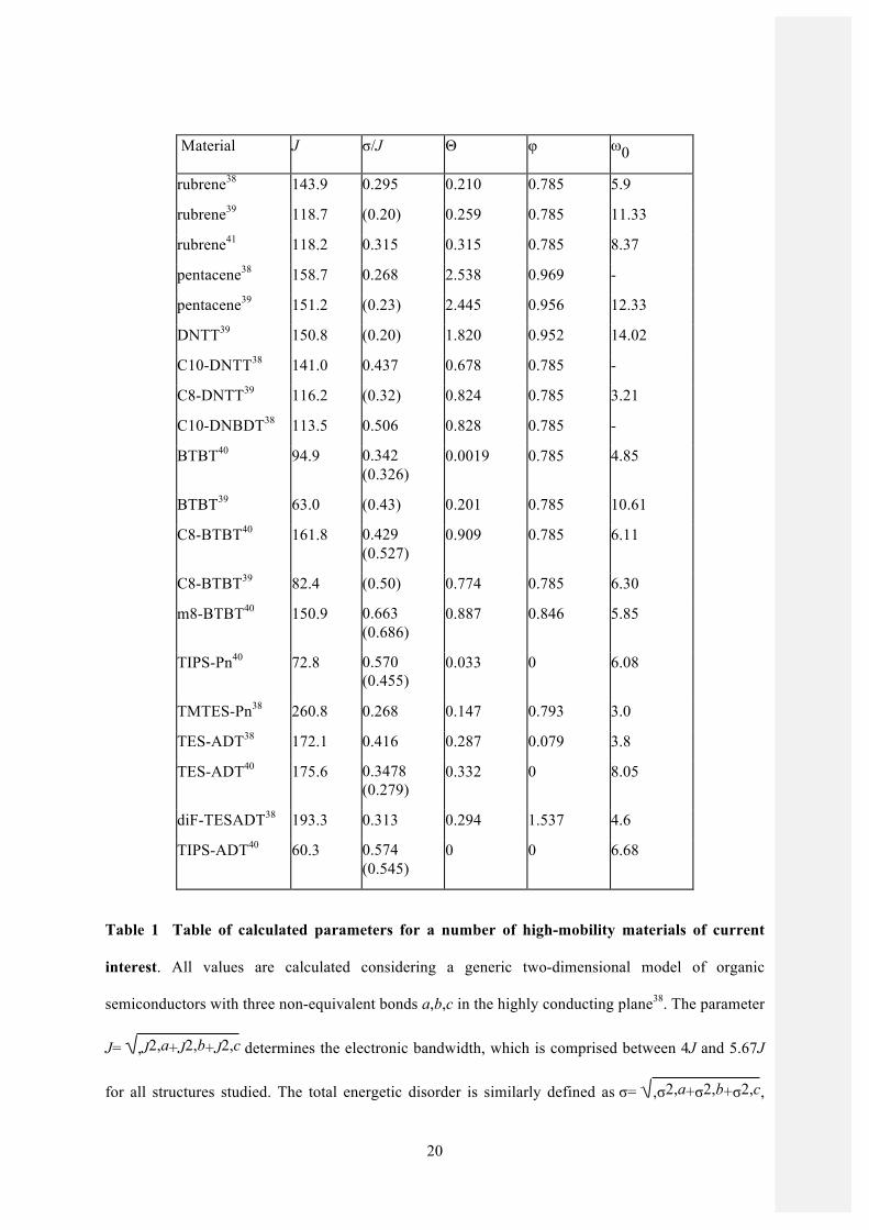
Material J σ/J Θ φ ω0
rubrene38 143.9 0.295 0.210 0.785 5.9
rubrene39 118.7 (0.20) 0.259 0.785 11.33
rubrene41 118.2 0.315 0.315 0.785 8.37
pentacene38 158.7 0.268 2.538 0.969 -
pentacene39 151.2 (0.23) 2.445 0.956 12.33
DNTT39 150.8 (0.20) 1.820 0.952 14.02
C10-DNTT38 141.0 0.437 0.678 0.785 -
C8-DNTT39 116.2 (0.32) 0.824 0.785 3.21
C10-DNBDT38 113.5 0.506 0.828 0.785 -
BTBT40 94.9 0.342 (0.326)
0.0019 0.785 4.85
BTBT39 63.0 (0.43) 0.201 0.785 10.61
C8-BTBT40 161.8 0.429 (0.527)
0.909 0.785 6.11
C8-BTBT39 82.4 (0.50) 0.774 0.785 6.30
m8-BTBT40 150.9 0.663 (0.686)
0.887 0.846 5.85
TIPS-Pn40 72.8 0.570 (0.455)
0.033 0 6.08
TMTES-Pn38 260.8 0.268 0.147 0.793 3.0
TES-ADT38 172.1 0.416 0.287 0.079 3.8
TES-ADT40 175.6 0.3478 (0.279)
0.332 0 8.05
diF-TESADT38 193.3 0.313 0.294 1.537 4.6
TIPS-ADT40 60.3 0.574 (0.545)
0 0 6.68
Table 1 Table of calculated parameters for a number of high-mobility materials of current
interest. All values are calculated considering a generic two-dimensional model of organic
semiconductors with three non-equivalent bonds a,b,c in the highly conducting plane38. The parameter
J= ,J2,a+J2,b+J2,c determines the electronic bandwidth, which is comprised between 4J and 5.67J
for all structures studied. The total energetic disorder is similarly defined as σ= ,σ2,a+σ2,b+σ2,c,
21
and refers here to inter-molecular vibrations alone (values between parentheses correspond to
calculations where only Gamma-point vibrations are included). The band anisotropy is identified by
two angles Θ and φ such that Ja=JcosΘ, Jb=JsinΘcosφ, Jc=JsinΘsinφ. The optimal isotropic structure
corresponds to Θ=Θ0=0.955 and φ=π/4=0.785. The appreciable spread of values reported for a given
material are indicative of the differences obtained between different methods.

22
Figure 1 Most commonly observed molecular packings in crystals of molecular organic
semiconductors and corresponding benchmark materials (top view; hydrogen atoms, side
chains and rings are omitted for clarity). a-b, The slipped-stack (a, example of α-phase of copper
phthalocyanine92) and slipped π-stack packings (b, rubrene93) only present one major transfer integral
(J1). c, The brick-wall packing (TIPS-Pentacene94) gives access to another transfer integral (J2). d, A
third transfer integral (J3) is accessible within the herringbone packing (C10-DNBDT-NW10),
allowing a more isotropic transport in the x-y plane.
23
Figure 2 Experimental characterisation of charge transport in molecular crystals. a, Angle
resolved Highest-Occupied Molecular Orbital (HOMO) band map of rubrene single-crystal along the
𝛤𝛶 direction at 300K exhibiting a gap, signature of hole coupling with intramolecular vibrations.15 b,
Real (top) and imaginary (bottom) part of the optical conductivity of rubrene below 2 THz at room
temperature (red) and 50K (blue) in optical-pump terahertz-probe spectroscopy.21 The lines indicate
fits to a modified Drude model (dashed) and a transient localization model (solid) c, Temperature and
pressure dependence of the coherence factor determined by Hall measurements on a pentacene single-
crystal. Below 220 K and at pressures of 1 GPa a fully coherent charge transport emerges.25 d,
Schematic illustration of the variation of strain in a C10-DNBDT-NW single-crystal OFET by
bending of the flexible substrate. e, Corresponding increase of the mobility under compressive strain
for three devices A (for which the four-terminal mobility is reported), B, C (for which two-terminal
saturated mobilities are reported).26. f, Histograms of the room temperature mobility for rubrene and
13C-rubrene single crystals, showing a small, but statistically significant suppression of mobility in the
heavier isotope that is consistent with predictions of the transient localization framework.27
24
Figure 3 Charge transport in small molecule and conjugated polymer semiconductors. a,
Schematic illustration of charge transport in molecular semiconductors in the transient localization
regime. Molecules are indicated by grey ellipses, τvib is the characteristic timescale of intermolecular
vibrations, the shaded orange regions indicate the spatial extent of the carrier wavefunction with
characteristic localisation length L. b, Illustration of charge transport in high mobility conjugated
polymers. Chains are indicated by grey lines, the orange shaded regions indicate the semi-crystalline
domains of the polymer and the red shaded regions the electron wavefunctions on different sections of
the chains with different degrees of localisation. c, Band-like temperature dependence of the 4-
terminal field-effect mobility (µ4T) and the Hall mobility (µHall) (left) and spin relaxation times T1 and
T2 (right) in a crystalline molecular semiconductor (C10-DNBDT-NW)88. The temperature dependence
of the momentum relaxation time τp extracted from the drift mobility is also shown. The percentage
values given indicate the errors in the measurement of T1, T2 and τp. The dashed lines indicate two
contributions to T2 from Elliott-Yafet spin relaxation (T2,EY) and motional narrowing (T2,MN). d,
Corresponding thermally activated temperature dependence of mobility and spin relaxation times in a
conjugated polymer (IDT-BT)89. Despite the clear difference in the temperature dependence of the
mobility the two systems exhibit a surprising similarity in the temperature dependence of the spin
25
relaxation times. Below 50K a transition from a Lorentzian electron spin resonance (ESR) lineshape
to a Voigtian lineshape is observed.
26
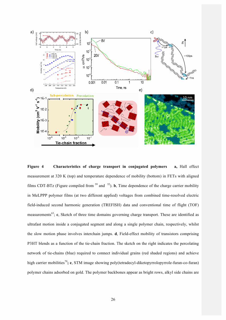
Figure 4 Characteristics of charge transport in conjugated polymers a, Hall effect
measurement at 320 K (top) and temperature dependence of mobility (bottom) in FETs with aligned
films CDT-BTz (Figure compiled from 59 and 52). b, Time dependence of the charge carrier mobility
in MeLPPP polymer films (at two different applied) voltages from combined time-resolved electric
field-induced second harmonic generation (TREFISH) data and conventional time of flight (TOF)
measurements63; c, Sketch of three time domains governing charge transport. These are identified as
ultrafast motion inside a conjugated segment and along a single polymer chain, respectively, whilst
the slow motion phase involves interchain jumps. d, Field-effect mobility of transistors comprising
P3HT blends as a function of the tie-chain fraction. The sketch on the right indicates the percolating
network of tie-chains (blue) required to connect individual grains (red shaded regions) and achieve
high carrier mobilities70; e, STM image showing poly(tetradecyl-diketopyrrolopyrrole-furan-co-furan)
polymer chains adsorbed on gold. The polymer backbones appear as bright rows, alkyl side chains are

27
seen as darker rows perpendicular to the backbones. Kinks and segmentation of the backbone are
clearly visible.85
28
Box 1 – Structure-property relationships in molecular semiconductors and conjugated polymers –
Some key examples
Rubrene and pentacene used to be the most widely studied, prototypical molecular semiconductors95,
but in recent years organic chemistry has provided access to a wide range of new molecules that have
allowed a more comprehensive and microscopic understanding of the key requirements for achieving
high carrier mobilities and of the underpinning charge transport physics. Here we provide only a few
examples. A key breakthrough was the discovery of highly soluble and chemically stable brick-wall
materials, including 6,13-bis(triisopropylsilylethynyl)pentacene (TIPS-Pentacene) and 2,8-difluoro-
5,11-bis(triethylsilylethynyl)anthradithiophene (diF-TES-ADT), the latter exhibits charge carrier
mobilities up to 6 cm2V-1s-1 in single crystals.94,96 Similarly influential was the report of herringbone-
stacked alkylated thienoacene-based materials, [1]benzothieno[3,2-b][1]benzothiophene (BTBT)97,
dinaphtho[2,3-b:2',3'-f]thieno[3,2-b]thiophene (DNTT)98, dibenzothiopheno[6,5-b:6 ′ ,5 ′ -
f]thieno[3,2-b]thiophene (DBTTT)99 as well as liquid crystalline derivatives thereof100. These give
access to charge carrier mobilities in excess of 10 cm2V-1s-1 and exhibit similar transport signatures
to rubrene, including a fully developed, “ideal” Hall effect, for which the Hall resistance scales
inversely with the carrier concentration.97–99 Another important, more recent development has been
the investigation of thienoacenes with a bent-shaped core (V, N or zig-zag shape), which exhibit some
of the highest mobilities observed so far, presumably as a result of a shape-induced suppression of
molecular vibrations.10,45,101 Solution-processed single-crystals of the alkylated N-shape 3,11-
dialkyldinaphtho[2,3-d:2’,3’-d’]benzo[1,2-b:4,5-b’]dithiophene (DNBDT-NW) exhibit mobilities up
to 15 cm2 V-1 s-1 combined with the lowest flicker noise ever reported in rationally designed molecular
solids.88,102 These molecules have all been studied in p-type OFET configurations. To realize n-type
OFETs molecules are needed with deeper lowest unoccupied molecular orbital (LUMO) states, but
the relevant transport physics is otherwise presumed similar. To date, the best performing n-type
materials exhibit a brick-wall packing, a fully isotropic herringbone n-type material has to the best of
our knowledge not been demonstrated yet. Among the brick-wall napthalene and perylene
tetracarboxilic diimides derivatives, N,N’-bis(1H,1H-perfluorobutyl)-(1,7&1,6)-dicyanoperylene-
29
3,4:9,10-bis(dicarboximide) (PDIF-CN2) exhibits a mobility of up to 5 cm2 V-1 s-1 at room
temperature and an ideal Hall signature.46,103,104 These values are similar to those achieved on the
brick-wall p-type counterpart, diF-TES-ADT. Fullerenes, such as C60, have achieved similarly high
mobility values. 105
For many of these molecular systems single crystals are available for transport studies; in devices
based on polycrystalline films extensive optimisation of film microstructure and morphology is crucial
to approach the performance achievable in single crystals (for a review see 9). In polymeric systems,
for which usually no single crystals are available, characterisation and control of thin film
microstructure moves even more centre-stage. For many years research focussed on polymers with
relatively simple repeat unit structures, including the polythiophene polymers poly-3-hexylthiophene
(P3HT)106,107 and PBTTT108 that exhibit mobilities up to 0.1-0.5 cm2V-1s-1. These polymers have
characteristic semi-crystalline microstructures, in which relatively highly ordered crystalline domains
- which adopt preferential edge-on or also face-on orientation with respect to the substrate - are
embedded within a disordered amorphous matrix which accommodate the distribution of chains
lengths and chain ends. However, even within the crystalline domains there is significant
paracrystalline disorder, that is absence of long-range order despite well-defined short- and medium
range order. This is caused, for example, by variations in the π−π stacking distances 109. Recently
interest has shifted to polymers with more complex backbone structures, in particular so-called
donor-acceptor (D-A) co-polymers comprising alternating electron-rich and electron deficient units
along the backbone. There is a broad range of these polymers, comprising building blocks based on
indacenodithiophene (IDT), diketopyrrolopyrrole (DPP), naphtalenediimide (NDI),
cyclopentadithiophene (CDT), benzothiadiazole (BT), thiophene (T) or isoindigo (IIT), whose field-
effect mobilities now commonly exceed 1 cm2/Vs. A puzzling feature given the high mobilities is that
the microstructure of these D-A copolymers tends to be less crystalline than that of P3HT/PBTTT: X-
ray diffraction typically reveals some degree of either edge-on or face-on crystalline order110 , but
often with fewer higher order and broader diffraction peaks than, for example PBTTT. In some
systems, such as Indacenodithiophene-Benzothiadiazole (IDT-BT)55 or Dithiopheneindenofluorene-
Benzothiadiazole (TIF-BT)111, both exhibiting charge carrier mobilities on the order of 2-3 cm2/Vs,
30
there is even evidence for only local chain aggregation and formation of close contact points86, but
not pronounced semicrystalline order and their microstructure appears nearly amorphous.112 This is
an advantage for technological applications which require uniform electronic properties over large
areas.
31
Box 2 - Effect of ions on electronic structure
Incorporation of ions into a conjugated polymer modifies the electronic structure significantly and
may generate electronic carriers by doping: For organic charge transfer dopants, doping can either
involve integer electron transfer from the organic host onto the dopant or the formation of a charge
transfer complex113. Other methods of doping involve the uses of acids/bases or electrolytes. Recent
theoretical work has provided clear insight into the factors that govern full dopant ionization114. In all
cases the incorporation of the dopant molecules into the organic film tends to introduce additional
structural disorder, and the strong Coulombic interactions between the electronic carriers and the
charge-stabilizing counterions can provide an additional driving force for localisation of the
electronic carriers. Nevertheless, surprisingly high electronic mobilities have been observed in some
of these mixed ionic-electronic conduction systems, which in some cases exceed the values observed
in field-effect gated structures115. Such high mobilities are usually attributed to two effects. On one
hand, bulk chemical or electrochemical doping leads to high charge densities; mobility increases with
charge density due to trap passivation and access to more delocalized electronic states116. On the
other hand, transport in these films occurs in the bulk, taking on an essentially 3D character as
opposed to the 2D character imposed in field-effect devices. This surprising robustness of the
electronic transport to ionic disorder remains to be much better understood. The interplay between
order and disorder is indeed more complex in bulk doped systems and even more so in mixed
electronic-ionic conductors, where also ions exhibit non-negligible mobility. For instance, disordered
regions are detrimental to transport while providing favourable sites for dopant diffusion. The
ordering of the ions (that is their incorporation into well-defined sites within the polymer structure),
which leads to control of the distance between the ions and electrons, appears to be a key factor117.
However, more detailed structural identification of the specific sites into which the dopants are
incorporated in these systems is needed. The electronic structure of these systems also remains
insufficiently well understood. It is typically observed that electronic carrier mobilities are low at low
doping densities, when carriers are presumed to remain bound by individual counterions118. To
achieve high conductivities and high carrier mobilities it is necessary to incorporate large doping
densities on the order of 10%. It is presumed that at such high doping densities the individual
32
Coulomb potentials start to overlap and allow the carriers to become mobile. Better techniques are
needed to estimate the density of states broadening due to the Coulombic interactions with the ions, as
well as the effects of on-site Coulomb repulsion for doubly occupied polymer sites119 need to be better
understood.
33
References
1. Guo, X. et al. Current Status and Opportunities of Organic Thin-Film Transistor Technologies. IEEE Trans. Electron Devices 64, 1906–1921 (2017).
2. Rivnay, J. et al. Organic electrochemical transistors. Nat. Rev. Mater. 3, 17086 (2018).
3. Russ, B., Glaudell, A., Urban, J. J., Chabinyc, M. L. & Segalman, R. A. Organic thermoelectric materials for energy harvesting and temperature control. Nature Reviews Materials 1, 16050 (2016).
4. Van De Burgt, Y., Melianas, A., Keene, S. T., Malliaras, G. & Salleo, A. Organic electronics for neuromorphic computing. Nature Electronics 1, 386–397 (2018).
5. Someya, T., Bao, Z. & Malliaras, G. G. The rise of plastic bioelectronics. Nature 540, 379–385 (2016).
6. Choi, H. H., Cho, K., Frisbie, C. D., Sirringhaus, H. & Podzorov, V. Critical assessment of charge mobility extraction in FETs. Nature Materials 17, 2–7 (2017).
7. Liu, C. et al. Device Physics of Contact Issues for the Overestimation and Underestimation of Carrier Mobility in Field-Effect Transistors. Phys. Rev. Appl. 8, 034020 (2017).
8. Dong, H., Fu, X., Liu, J., Wang, Z. & Hu, W. 25th Anniversary Article: Key Points for High-Mobility Organic Field-Effect Transistors. Advanced Materials 25, 6158–6183 (2013).
9. Zhao, Y., Guo, Y. & Liu, Y. 25th Anniversary Article: Recent Advances in n-Type and Ambipolar Organic Field-Effect Transistors. Adv. Mater. 25, 5372–5391 (2013).
10. Mitsui, C. et al. High-Performance Solution-Processable N-Shaped Organic Semiconducting Materials with Stabilized Crystal Phase. Adv. Mater. 26, 4546–4551 (2014).
11. Schweicher, G. et al. Bulky End-Capped [1]Benzothieno[3,2-b]benzothiophenes: Reaching High-Mobility Organic Semiconductors by Fine Tuning of the Crystalline Solid-State Order. Adv. Mater. 1–7 (2015). doi:10.1002/adma.201500322
12. Podzorov, V. et al. Intrinsic charge transport on the surface of organic semiconductors. Phys. Rev. Lett. 93, 1–4 (2004).
13. Schweicher, G., Olivier, Y., Lemaur, V. & Geerts, Y. H. What currently limits charge carrier mobility in crystals of molecular semiconductors? Isr. J. Chem. 54, 595–620 (2014).
14. MacHida, S. I. et al. Highest-occupied-molecular-orbital band dispersion of rubrene single crystals as observed by angle-resolved ultraviolet photoelectron spectroscopy. Phys. Rev. Lett. 104, 156401 (2010).
15. Bussolotti, F. et al. Hole-phonon coupling effect on the band dispersion of organic molecular semiconductors. Nat. Commun. 8, 173 (2017).
16. Ciuchi, S. & Fratini, S. Band Dispersion and Electronic Lifetimes in Crystalline Organic Semiconductors. Phys. Rev. Lett. 106, 166403 (2011).
17. Ciuchi, S. et al. Molecular Fingerprints in the Electronic Properties of Crystalline Organic Semiconductors: From Experiment to Theory. Phys. Rev. Lett. 108, 256401 (2012).
18. Eggeman, A. S., Illig, S., Troisi, A., Sirringhaus, H. & Midgley, P. a. Measurement of molecular motion in organic semiconductors by thermal diffuse electron scattering. Nat. Mater. 12, 1045–9 (2013).
19. Illig, S. et al. Reducing dynamic disorder in small-molecule organic semiconductors by suppressing large-Amplitude thermal motions. Nat. Commun. 7, 1–10 (2016).
34
20. Gershenson, M. E., Podzorov, V. & Morpurgo, A. F. Colloquium: Electronic transport in single-crystal organic transistors. Rev. Mod. Phys. 78, 973–989 (2006).
21. Yada, H. et al. Carrier dynamics of rubrene single-crystals revealed by transient broadband terahertz spectroscopy. Appl. Phys. Lett. 105, 143302 (2014).
22. Li, Z. Q. et al. Light quasiparticles dominate electronic transport in molecular crystal field-effect transistors. Phys. Rev. Lett. 99, 016403 (2007).
23. Fischer, M., Dressel, M., Gompf, B., Tripathi, A. K. & Pflaum, J. Infrared spectroscopy on the charge accumulation layer in rubrene single crystals. Appl. Phys. Lett. 89, 182103 (2006).
24. Meneau, A. Y. B. et al. Temperature dependence of charge localization in high-mobility, solution-crystallized small molecule semiconductors studied by charge modulation spectroscopy. Adv. Funct. Mater. 26, 2326–2333 (2016).
25. Sakai, K. et al. The emergence of charge coherence in soft molecular organic semiconductors via the suppression of thermal fluctuations. NPG Asia Mater. 8, e252 (2016).
26. Kubo, T. et al. Suppressing molecular vibrations in organic semiconductors by inducing strain. Nat. Commun. 7, 11156 (2016).
27. Ren, X. et al. Negative Isotope Effect on Field-Effect Hole Transport in Fully Substituted 13C-Rubrene. Adv. Electron. Mater. 3, 1700018 (2017).
28. Hussey, N. E., Takenaka, K. & Takagi, H. Universality of the Mott-Ioffe-Regel limit in metals. Philos. Mag. 84, 2847–2864 (2004).
29. Fratini, S., Mayou, D. & Ciuchi, S. The transient localization scenario for charge transport in crystalline organic materials. Advanced Functional Materials 26, 2292–2315 (2016).
30. Fratini, S. & Ciuchi, S. On dynamical localization corrections to band transport. arXiv:1903.12603 (2019).
31. Troisi, A. & Orlandi, G. Charge-transport regime of crystalline organic semiconductors: Diffusion limited by thermal off-diagonal electronic disorder. Phys. Rev. Lett. 96, 086601 (2006).
32. Ciuchi, S., Fratini, S. & Mayou, D. Transient localization in crystalline organic semiconductors. Phys. Rev. B 83, 081202 (2011).
33. Giannini, S. et al. Quantum localization and delocalization of charge carriers in organic semiconducting crystals. Nat. Commun. 10, 3843 (2019).
34. Ortmann, F., Bechstedt, F. & Hannewald, K. Charge transport in organic crystals: Theory and modelling. Phys. status solidi 248, 511–525 (2011).
35. Wang, L., Prezhdo, O. V & Beljonne, D. Mixed quantum-classical dynamics for charge transport in organics. Physical Chemistry Chemical Physics 17, 12395–12406 (2015).
36. Giannini, S., Carof, A. & Blumberger, J. Crossover from Hopping to Band-Like Charge Transport in an Organic Semiconductor Model: Atomistic Nonadiabatic Molecular Dynamics Simulation. J. Phys. Chem. Lett. 9, 3116–3123 (2018).
37. Wang, L. et al. Computational methods for design of organic materials with high charge mobility. Chemical Society Reviews 39, 423–434 (2010).
38. Fratini, S., Ciuchi, S., Mayou, D., De Laissardière, G. T. & Troisi, A. A map of high-mobility molecular semiconductors. Nat. Mater. 16, 998–1002 (2017).
39. Schweicher, G. et al. Chasing the “Killer” Phonon Mode for the Rational Design of Low�Disorder, High�Mobility Molecular Semiconductors. Adv. Mater. 31, 1902407 (2019).
35
40. Harrelson, T. F. et al. Direct probe of the nuclear modes limiting charge mobility in molecular semiconductors. Mater. Horizons 6, 182–191 (2019).
41. Ruggiero, M. T., Ciuchi, S., Fratini, S. & D’Avino, G. Electronic Structure, Electron-Phonon Coupling, and Charge Transport in Crystalline Rubrene under Mechanical Strain. J. Phys. Chem. C 123, 15897–15907 (2019).
42. Ciuchi, S. & Fratini, S. Electronic transport and quantum localization effects in organic semiconductors. Phys. Rev. B 86, 245201 (2012).
43. Fratini, S., Ciuchi, S., Mayou, D., De Laissardière, G. T. & Troisi, A. A map of high-mobility molecular semiconductors. Nat. Mater. 16, 998–1002 (2017).
44. Lee, N. E., Zhou, J. J., Agapito, L. A. & Bernardi, M. Charge transport in organic molecular semiconductors from first principles: The bandlike hole mobility in a naphthalene crystal. Phys. Rev. B 97, 115203 (2018).
45. Okamoto, T. et al. V-Shaped Organic Semiconductors With Solution Processability, High Mobility, and High Thermal Durability. Adv. Mater. 25, 6392–6397 (2013).
46. Minder, N. A., Ono, S., Chen, Z., Facchetti, A. & Morpurgo, A. F. Band-Like Electron Transport in Organic Transistors and Implication of the Molecular Structure for Performance Optimization. Adv. Mater. 24, 503–508 (2012).
47. Vladimirov, I., Kühn, M., Geßner, T., May, F. & Weitz, R. T. Energy barriers at grain boundaries dominate charge carrier transport in an electron-conductive organic semiconductor. Sci. Rep. 8, 14868 (2018).
48. Nielsen, C. B., Turbiez, M. & McCulloch, I. Recent advances in the development of semiconducting DPP-containing polymers for transistor applications. Advanced Materials 25, 1859–1880 (2013).
49. Wang, E., Mammo, W. & Andersson, M. R. 25th Anniversary Article : Isoindigo-Based Polymers and Small Molecules for Bulk Heterojunction Solar Cells and Field Effect Transistors. Adv. Mater. 1801–1826 (2014).
50. Hoi, B. et al. The Influence of Morphology on High-Performance Polymer Field-Effect Transistors. Adv. Mater. 21, 209–212 (2009).
51. Kastler, M. et al. A high-mobility electron-transporting polymer for printed transistors. Nature 457, 679–686 (2009).
52. Yamashita, Y. et al. Mobility Exceeding 10 cm 2 /(V · s) in Donor − Acceptor Polymer Transistors with Band-like Charge Transport. Chem. Mater. 28, 420–424 (2016).
53. Schott, S. et al. Charge-Transport Anisotropy in a Uniaxially Aligned Diketopyrrolopyrrole-Based Copolymer. Adv. Mater. 27, 7356–7364 (2015).
54. Bucella, S. G. et al. Macroscopic and high-throughput printing of aligned nanostructured polymer semiconductors for MHz large-area electronics. Nat. Commun. 6, 8394 (2015).
55. Venkateshvaran, D. et al. Approaching disorder-free transport in high-mobility conjugated polymers. Nature 515, 384–388 (2014).
56. Xu, Y. et al. Exploring the Charge Transport in Conjugated Polymers. Adv. Mater. 29, 1702729 (2017).
57. Kronemeijer, A. J. et al. Two-dimensional carrier distribution in top-gate polymer field-effect transistors: Correlation between width of density of localized states and urbach energy. Adv. Mater. 26, 728–733 (2014).
36
58. Senanayak, S. P., Ashar, A. Z., Kanimozhi, C., Patil, S. & Narayan, K. S. Room-temperature bandlike transport and Hall effect in a high-mobility ambipolar polymer. Phys. Rev. B - Condens. Matter Mater. Phys. 91, 115302 (2015).
59. Yamashita, Y. et al. Transition between band and hopping transport in polymer field-effect transistors. Adv. Mater. 26, 8169–8173 (2014).
60. Steyrleuthner, B. R. et al. Bulk Electron Transport and Charge Injection in a High Mobility n-Type Semiconducting Polymer. Adv. Mater. 22, 2799–2803 (2010).
61. Nikolka, M. et al. High-mobility, trap-free charge transport in conjugated polymer diodes. Nat. Commun. 10, 2122 (2019).
62. Abramavicius, V., Pranculis, V., Melianas, A., Inganäs, O. & Gulbinas, V. Role of coherence and delocalization in photo-induced electron transfer at organic interfaces. Sci. Rep. 6, 32914 (2016).
63. Devižis, A., Meerholz, K., Hertel, D. & Gulbinas, V. Hierarchical charge carrier motion in conjugated polymers. Chem. Phys. Lett. 498, 302–306 (2010).
64. Noriega, R., Salleo, A. & Spakowitz, A. J. Chain conformations dictate multiscale charge transport phenomena in disordered semiconducting polymers. 8, 16315–16320 (2013).
65. Hendry, E. et al. Interchain effects in the ultrafast photophysics of a semiconducting polymer: THz time-domain spectroscopy of thin films and isolated chains in solution. Phys. Rev. B 71, 125201 (2005).
66. Prins, P. et al. High Intrachain Hole Mobility on Molecular Wires of Ladder-Type Poly( p -Phenylenes). Phys. Rev. Lett. 96, 146601 (2006).
67. Noriega, R. et al. A general relationship between disorder, aggregation and charge transport in conjugated polymers. Nat. Mater. 12, 1038–44 (2013).
68. Statz, M. et al. On the manifestation of electron-electron interactions in the thermoelectric response of semicrystalline conjugated polymers with low energetic disorder. Commun. Phys. 1, 16 (2018).
69. Mollinger, S. A., Krajina, B. A., Noriega, R., Salleo, A. & Spakowitz, A. J. Percolation, Tie-Molecules, and the Microstructural Determinants of Charge Transport in Semicrystalline Conjugated Polymers. ACS Macro Lett. 4, 708–712 (2015).
70. Gu, K. et al. Assessing the Huang-Brown Description of Tie Chains for Charge Transport in Conjugated Polymers. ACS Macro Lett. 7, 1333–1338 (2018).
71. Watts, B., Schuettfort, T. & McNeill, C. R. Mapping of domain orientation and molecular order in polycrystalline semiconducting polymer films with soft X-ray microscopy. Adv. Funct. Mater. 21, 1122–1131 (2011).
72. Jimison, L. H., Toney, M. F., McCulloch, I., Heeney, M. & Salleo, A. Charge-Transport Anisotropy Due to Grain Boundaries in Directionally Crystallized Thin Films of Regioregular Poly(3-hexylthiophene). Adv. Mater. 21, 1568–1572 (2009).
73. Martin, D. C., Martin, D. C. & Thomas, E. L. Grain boundaries in extended-chain polymers: Theory and experiment. Philos. Mag. A Phys. Condens. Matter, Struct. Defects Mech. Prop. 64, 903–922 (1991).
74. Takacs, C. J., Brady, M. A., Treat, N. D., Kramer, E. J. & Chabinyc, M. L. Quadrites and Crossed-Chain Crystal Structures in Polymer Semiconductors. Nano Lett 14, 3101 (2014).
75. Rühle, V. et al. Microscopic simulations of charge transport in disordered organic semiconductors. Journal of Chemical Theory and Computation 7, 3335–3345 (2011).
37
76. Martinelli, N. et al. Charge Transport in Organic Semiconductors: A Multiscale Modeling. in Functional Supramolecular Architectures: For Organic Electronics and Nanotechnology 1, 1–38 (wiley, 2010).
77. Kirkpatrick, J., Marcon, V., Nelson, J., Kremer, K. & Andrienko, D. Charge mobility of discotic mesophases: A multiscale quantum and classical study. Phys. Rev. Lett. 98, 227402 (2007).
78. McMahon, D. P. et al. Relation between microstructure and charge transport in polymers of different regioregularity. J. Phys. Chem. C 115, 19386–19393 (2011).
79. Poelking, C. et al. Characterization of charge-carrier transport in semicrystalline polymers: Electronic couplings, site energies, and charge-carrier dynamics in poly(bithiophene-alt-thienothiophene) [PBTTT]. J. Phys. Chem. C 117, 1633–1640 (2013).
80. Liu, T. & Troisi, A. Understanding the microscopic origin of the very high charge mobility in PBTTT: Tolerance of thermal disorder. Adv. Funct. Mater. 24, 925–933 (2014).
81. Schulz, G. L. et al. The PCPDTBT Family: Correlations between Chemical Structure, Polymorphism, and Device Performance. Macromolecules 50, 1402–1414 (2017).
82. Fornari, R. P. & Troisi, A. Theory of charge hopping along a disordered polymer chain. Phys. Chem. Chem. Phys. 16, 9997–10007 (2014).
83. Fornari, R. P. & Troisi, A. Narrower bands with better charge transport: The counterintuitive behavior of semiconducting copolymers. Adv. Mater. 26, 7627–7631 (2014).
84. Fornari, R. P., Blom, P. W. M. & Troisi, A. How Many Parameters Actually Affect the Mobility of Conjugated Polymers? Phys. Rev. Lett. 118, (2017).
85. Warr, D. A. et al. Sequencing conjugated polymers by eye. Sci. Adv. 4, eaas9543 (2018).
86. Thomas, T. H. et al. Short contacts between chains enhancing luminescence quantum yields and carrier mobilities in conjugated copolymers. Nat. Commun. 10, 2614 (2019).
87. Anderson, M. et al. Displacement of polarons by vibrational modes in doped conjugated polymers. Phys. Rev. Mater. 1, 055604 (2017).
88. Tsurumi, J. et al. Coexistence of ultra-long spin relaxation time and coherent charge transport in organic single-crystal semiconductors. Nat. Phys. 13, 994–998 (2017).
89. Schott, S. et al. Polaron spin dynamics in high-mobility polymeric semiconductors. Nat. Phys. 1 (2019). doi:10.1038/s41567-019-0538-0
90. Kambe, T. et al. π-Conjugated nickel bis(dithiolene) complex nanosheet. J. Am. Chem. Soc. 135, 2462–2465 (2013).
91. Paulsen, B. D., Tybrandt, K., Stavrinidou, E. & Rivnay, J. Organic mixed ionic–electronic conductors. Nat. Mater. (2019). doi:10.1038/s41563-019-0435-z
92. Hoshino, A., Takenaka, Y. & Miyaji, H. Redetermination of the crystal structure of α-copper phthalocyanine grown on KCl. Acta Crystallogr. Sect. B Struct. Sci. 59, 393–403 (2003).
93. Jurchescu, O. D., Meetsma, A. & Palstra, T. T. M. Low-temperature structure of rubrene single crystals grown by vapor transport. Electrochem. Solid-State Lett. 9, 330–334 (2006).
94. Anthony, J. E., Brooks, J. S., Eaton, D. L. & Parkin, S. R. Functionalized pentacene: Improved electronic properties from control of solid-state order. Journal of the American Chemical Society 123, 9482–9483 (2001).
95. Podzorov, V., Menard, E., Rogers, J. a. & Gershenson, M. E. Hall effect in the accumulation layers on the surface of organic semiconductors. Phys. Rev. Lett. 95, 1–4 (2005).
38
96. Jurchescu, O. D. et al. Organic single-crystal field-effect transistors of a soluble anthradithiophene. Chem. Mater. 20, 6733–6737 (2008).
97. Ebata, H. et al. Highly soluble [1]benzothieno[3,2-b]benzothiophene (BTBT) derivatives for high-performance, solution-processed organic field-effect transistors. J. Am. Chem. Soc. 129, 15732–15733 (2007).
98. Kang, M. J. et al. Alkylated dinaphtho[2,3-b:2′,3′-f ]thieno[3,2-b]thiophenes (Cn-DNTTs): Organic semiconductors for high-performance thin-film transistors. Adv. Mater. 23, 1222–1225 (2011).
99. Park, J.-I. et al. Dibenzothiopheno[6,5-b:6’,5’-f]thieno[3,2-b]thiophene (DBTTT): High-Performance Small-Molecule Organic Semiconductor for Field-Effect Transistors. J. Am. Chem. Soc. 150331144501001 (2015). doi:10.1021/jacs.5b01108
100. Iino, H., Usui, T. & Hanna, J. I. Liquid crystals for organic thin-film transistors. Nat. Commun. 6, 6828 (2015).
101. Okamoto, T. Next-generation organic semiconductors driven by bent-shaped π-electron cores. Polym. J. (2019). doi:10.1038/s41428-019-0180-9
102. Watanabe, S. et al. Remarkably low flicker noise in solution-processed organic single crystal transistors. Commun. Phys. 1, 37 (2018).
103. Jones, B. A. et al. High-mobility air-stable n-type semiconductors with processing versatility: Dicyanoperylene-3,4:9,10-bis(dicarboximides). Angew. Chemie - Int. Ed. 43, 6363–6366 (2004).
104. He, T. et al. Single-crystal field-effect transistors of new Cl2-NDI polymorph processed by sublimation in air. Nat. Commun. 6, 5954 (2015).
105. Li, H. et al. High-Mobility Field-Effect Transistors from Large-Area Solution-Grown Aligned C 60 Single Crystals. J. Am. Chem. Soc. 134, 2760–2765 (2012).
106. Sirringhaus, H. et al. Two-dimensional charge transport in self-organized, high-mobility conjugated polymers. Nature 401, 685–688 (1999).
107. Bao, Z., Dodabalapur, A. & Lovinger, A. J. Soluble and processable regioregular poly(3-hexylthiophene) for thin film field-effect transistor applications with high mobility. Appl. Phys. Lett. 69, 4108–4110 (1996).
108. McCulloch, I. et al. Liquid-crystalline semiconducting polymers with high charge-carrier mobility. Nat. Mater. 5, 328–333 (2006).
109. Rivnay, J. et al. Structural origin of gap states in semicrystalline polymers and the implications for charge transport. RAPID Commun. Phys. Rev. B 83, 121306 (2011).
110. Mei, J., Kim, D. H., Ayzner, A. L., Toney, M. F. & Bao, Z. Siloxane-Terminated Solubilizing Side Chains: Bringing Conjugated Polymer Backbones Closer and Boosting Hole Mobilities in Thin-Film Transistors. J. Am. Chem. Soc. 133, 20130–20133 (2011).
111. Chen, H. et al. Dithiopheneindenofluorene (TIF) Semiconducting Polymers with Very High Mobility in Field-Effect Transistors. Adv. Mater. 29, 1702523 (2017).
112. Zhang, X. et al. Molecular origin of high field-effect mobility in an indacenodithiophene- benzothiadiazole copolymer. Nat. Commun. 4, 2238 (2013).
113. Jacobs, I. E. & Moulé, A. J. Controlling Molecular Doping in Organic Semiconductors. Advanced Materials 29, 1703063 (2017).
114. Li, J. et al. Correlated electron-hole mechanism for molecular doping in organic
39
semiconductors. Phys. Rev. Mater. 1, 025602 (2017).
115. Cendra, C. et al. Role of the Anion on the Transport and Structure of Organic Mixed Conductors. Adv. Funct. Mater. 29, 1807034 (2019).
116. Hulea, I. N. et al. Wide energy-window view on the density of states and hole mobility in poly(p-phenylene vinylene). Physical Review Letters 93, 166601 (2004).
117. Kang, K. et al. 2D coherent charge transport in highly ordered conducting polymers doped by solid state diffusion. Nat. Mater. 15, 896–902 (2016).
118. Mityashin, A. et al. Unraveling the mechanism of molecular doping in organic semiconductors. Adv. Mater. 24, 1535–1539 (2012).
119. Png, R. Q. et al. Madelung and Hubbard interactions in polaron band model of doped organic semiconductors. Nat. Commun. 7, 11948 (2016).