Characterization of High-Resistivity Silicon
Bulk and Silicon-on-Insulator Wafers
by
Pinakpani Nayak
A Dissertation Presented in Partial Fulfillment of the Requirements for the Degree
Doctor of Philosophy
Approved August 2011 by the Graduate Supervisory Committee:
Dieter Schroder, Chair
Dragica Vasileska Michael Kozicki
James Aberle
ARIZONA STATE UNIVERSITY
August 2012

i
ABSTRACT
High-Resistivity Silicon (HRS) substrates are important for low-loss, high-
performance microwave and millimeter wave devices in high-frequency
telecommunication systems. The highest resistivity of up to ~10,000 ohm.cm is
Float Zone (FZ) grown Si which is produced in small quantities and moderate
wafer diameter. The more common Czochralski (CZ) Si can achieve resistivities
of around 1000 ohm.cm, but the wafers contain oxygen that can lead to thermal
donor formation with donor concentration significantly higher (~1015 cm-3) than
the dopant concentration (~1012-1013 cm-3) of such high-resistivity Si leading to
resistivity changes and possible type conversion of high-resistivity p-type silicon.
In this research capacitance–voltage (C–V) characterization is employed to study
the donor formation and type conversion of p-type High-resistivity Silicon-On-
Insulator (HRSOI) wafers and the challenges involved in C-V characterization of
HRSOI wafers using a Schottky contact are highlighted. The maximum
capacitance of bulk or Silicon-On-Insulator (SOI) wafers is governed by the
gate/contact area. During C-V characterization of high-resistivity SOI wafers with
aluminum contacts directly on the Si film (Schottky contact); it was observed that
the maximum capacitance is much higher than that due to the contact area,
suggesting bias spreading due to the distributed transmission line of the film
resistance and the buried oxide capacitance. In addition, an “S”-shape C–V plot
was observed in the accumulation region. The effects of various factors, such as:
frequency, contact and substrate sizes, gate oxide, SOI film thickness, film and
substrate doping, carrier lifetime, contact work-function, temperature, light,

ii
annealing temperature and radiation on the C-V characteristics of HRSOI wafers
are studied.
HRSOI wafers have the best crosstalk prevention capability compared to other
types of wafers, which plays a major role in system-on-chip configuration to
prevent coupling between high frequency digital and sensitive analog circuits.
Substrate crosstalk in HRSOI and various factors affecting the crosstalk, such as:
substrate resistivity, separation between devices, buried oxide (BOX) thickness,
radiation, temperature, annealing, light, and device types are discussed. Also
various ways to minimize substrate crosstalk are studied and a new
characterization method is proposed.
Owing to their very low doping concentrations and the presence of oxygen in
CZ wafers, HRS wafers pose a challenge in resistivity measurement using
conventional techniques such as four-point probe and Hall measurement methods.
In this research the challenges in accurate resistivity measurement using four-
point probe, Hall method, and C-V profile are highlighted and a novel approach
to extract resistivity of HRS wafers based on Impedance Spectroscopy
measurements using polymer dielectrics such as Polystyrene and Poly Methyl
Methacrylate (PMMA) is proposed.

iii
Dedicated
to
My Parents
Swarnalata Pradhan
Dhruba Charan Nayak

iv
ACKNOWLEDGMENTS
It has been my dream to complete my higher studies. And as I get a step closer
towards my dream, I would like to thank some of the most important people who
supported and helped me at various stages of my journey. First of all I am
thankful to my chair Dr. Dieter K. Schroder for accepting me as his student and
supporting me in every possible manner during my studies both professionally
and personally. He has been my teacher, my guide and my mentor, without whom
I would not have come this far. He is a wonderful teacher who has the unique
ability to teach the arduous concepts of semiconductor devices in a simple and
lucid manner comprehensible to the students. I am thankful to him for patiently
clarifying all my doubts many during and after office hours. He is one of the most
approachable and kindest teachers I have ever met. His affable manners and ever
pleasing personality make it a joy to work with him.
I am thankful to Dr. Dragica Vasileska for teaching me the concepts of device
modeling. She was very helpful during my research. I appreciate her valuable
suggestions to solve simulation problems encountered during this research.
I am thankful to Dr. James Aberle for teaching me the concepts of microwave
technology and helping me a lot during designing of the waveguides and taking
microwave measurements in the lab. He is a very helpful and wonderful teacher.
I thank Dr. Michael Kozicki for being a part of my PhD committee and
providing valuable suggestions for the thesis. His knowledge on semiconductor
processing and memories is unparalleled.

v
This research was partially funded by the Silicon Wafer Engineering and
Defect Science Consortium (SiWEDS) (Hynix Semiconductor, Intel Corp., LG
Siltron, MEMC Electronic Materials, Samsung Electronics, Siltronic, SOITEC,
and SUMCO TECHXIV). I thank G. Celler from Soitec USA and M. Seacrist
from MEMC Electronic Materials for supplying the SOI wafers for this research.
I thank Dr. Ranko Richert for his guidance during Impedance Spectroscopy
experiments and allowing me to use his lab and equipments. I thank all the
CSSER staff members Carrier Sinclair, Jon Martin, Paul Boland, Wayne Paulson,
Jerry Eller, and Arthur Handugan for all their support and help in fabricating the
devices required for this research. They were very courteous and helpful. I thank
Viet Nguyen for teaching me the finer techniques of cleanroom processing and
helping me during the processing work. I appreciate Scott Lapora and the
Engineering Technical Support team for providing prompt technical service and
the necessary modeling software. I thank Masoud Koochakzadeh, Vinod Prabhu
Nagarajan, Vivek Sharma, Sayantan Das, Lokendra Singh and Ullas Pathak for
their help during various stages of experimental work.
I owe my entire life to my parents, their selfless dedication and sacrifices.
Their lives as academicians inspired me to pursue a life as a researcher. My
mother was always there at every step of my life; she taught me patience and
perseverance. I feel very sad that she is not there anymore physically to see me
reach the goal, but I know she is always there with me and guiding me during all
my hard times. My father and my grandfather are the quintessential symbols of
personal achievement and dedication to one’s profession. My father is my role

vi
model. I am also lucky to have my brother who is always there beside me
encouraging and helping me in every possible manner. Thank you, Jinu, for
everything. I am thankful to my parent-in-laws for supporting me in my decision.
I cannot forget a special person, Gurudas Pai, my guide and mentor during my
professional career, who encouraged me and helped me to stay focused to pursue
my dream. Without his support I wouldn’t have even started the journey.
I thank my family and friends for their generous help and support. To name a
few, my friends, Manoj, Biranchi, Prabhat, Sanghamitra, Seema, Farzana and
Gokul for being there at various stages of this long journey. I am grateful to my
uncle Dr. Ashok Pradhan for teaching me the basics of electrical engineering and
instilling in me the value of higher studies.
Finally one person without whose constant care and unconditional support I
would not have reached the destination, my wife, Sumeeta. She gave me the
strength and confidence to leave my comfort zone and pursue higher studies. She
was there to encourage me when the going was tough and to push me when I
deviated from my goal. She changed the course of her personal and professional
life many-a-times so that I could focus on my studies. Thank you for everything.

vii
TABLE OF CONTENTS
Page
LIST OF TABLES ...............................................................................................xiv
LIST OF FIGURES............................................................................................... xv
CHAPTER 1. INTRODUCTION............................................................................ 1
1.1. Introduction and Motivation for this Research ................................. 1
1.2. What is New in this Research? ......................................................... 3
1.3. Background Literature Review for this Research............................. 4
1.4. Organization...................................................................................... 6
CHAPTER 2. HIGH-RESISTIVITY SILICON FABRICATION.......................... 9
2.1. Introduction – The Need for High-Resistivity Silicon...................... 9
2.1.1. Gallium Arsenide Substrates ................................................ 11
2.1.2. Silicon on Sapphire Substrates ............................................. 11
2.1.3. High-Resistivity Silicon-on-Insulator Substrates ................. 12
2.1.4. Bulk Silicon Substrates......................................................... 12
2.2. Key Characteristics of High-resistivity Silicon wafers................... 13
2.3. High-Resistivity Silicon Crystal Growth........................................ 13
2.3.1. Czochralski Crystal Growth Technique ............................... 14
2.3.2. Dopant Distribution in CZ crystals....................................... 18
2.3.3. Unintended Dopants in CZ crystals...................................... 19
2.3.4. Magnetic Field Czochralski Crystal Growth (MCZ)............ 20
2.3.5. Continuous Czochralski Crystal growth............................... 22
2.3.6. Float Zone Crystal Growth Technique ................................. 24

viii
Page
2.3.7. Silicon Wafer Manufacturing ............................................... 29
2.3.8. Comparison between CZ and FZ crystals............................. 31
2.4. Silicon On Insulator (SOI) Wafers ................................................. 32
2.5. SOI Fabrication Methods................................................................ 33
2.5.1. SIMOX ................................................................................. 35
2.5.2. Bonding and Etchback (BESOI)........................................... 37
2.5.3. Smart Cut™ Process............................................................. 38
2.5.4. Porous Si Based Process: ELTRAN..................................... 41
2.6. Oxygen in Silicon ........................................................................... 44
2.6.1. Atomic Configuration of Oxygen in Silicon ........................ 45
2.6.2. Electrical Characteristics of Oxygen in Silicon -
Thermal Donors ............................................................. 48
2.7. Conclusion ...................................................................................... 50
CHAPTER 3. DEVICE MODELING................................................................... 52
3.1. Introduction..................................................................................... 52
3.2. Device Modeling Approach............................................................ 54
3.3. Introduction to the SILVACO ATLAS Simulation Tool ............... 57
3.3.1. ATLAS Overview................................................................. 57
3.3.2. ATLAS Process Flow........................................................... 58
3.3.3. The Order of ATLAS Commands ........................................ 59
3.4. Simulation Approach in this Research............................................ 60
3.4.1. Numerical Methods Used ..................................................... 61

ix
Page
3.4.2. Physical Models Used .......................................................... 62
3.5. Conclusion ...................................................................................... 63
CHAPTER 4. C-V CHARACTERISTICS OF HIGH-RESISTIVITY SOI ......... 65
4.1. Introduction..................................................................................... 65
4.2. C-V Characterization Technique .................................................... 67
4.2.1. Which C-V Method to Choose for High-resistivity
Silicon? .......................................................................... 69
4.2.2. Where to Apply the DC Bias During C-V
Measurements? .............................................................. 70
4.3. Schottky Barrier Height .................................................................. 71
4.4. Device Fabrication.......................................................................... 75
4.5. Experimental Setup......................................................................... 76
4.6. Simulation Setup............................................................................. 77
4.7. Analysis of C-V Characteristics of HRSOI using Schottky
Contact ....................................................................................... 78
4.7.1. A New Effect of Bias Spreading .......................................... 78
4.7.2. Effect of Frequency .............................................................. 88
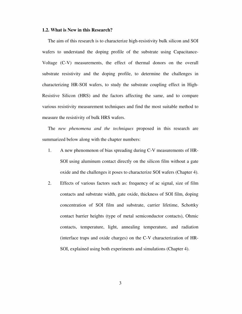
4.7.3. Effect of Contact and Substrate Size .................................... 90
4.7.4. Effect of Gate Oxide............................................................. 94
4.7.5. Effect of Film Thickness ...................................................... 96
4.7.6. Effect of Film Doping Concentration................................... 99
4.7.7. Effect of Substrate Doping Concentration.......................... 100

x
Page
4.7.8. Effect of Carrier Lifetime ................................................... 101
4.7.9. Effect of Contact Work-function........................................ 102
4.7.10. Effect of Radiation (Interface Charges and Interface
Traps) ........................................................................... 104
4.7.11. Effect of Light, Temperature, and Annealing................... 108
4.8. Conclusion .................................................................................... 109
CHAPTER 5. CROSSTALK IN HIGH-RESISTIVITY SILICON
WAFERS – BULK AND SILICON-ON-INSULATOR ...... 111
5.1. Introduction................................................................................... 111
5.2. What is Substrate Crosstalk – Mechanism and Factors
Affecting It?............................................................................. 112
5.3. Crosstalk Measurement Procedure ............................................... 117
5.3.1. Coplanar Wave Guide (CPW) ............................................ 117
5.3.2. S-Parameter ........................................................................ 118
5.4. VNA Calibration Techniques ....................................................... 122
5.4.1. Calibration Options and Standards ..................................... 124
5.4.2. SOLT (SHORT-OPEN-LOAD-THRU) Calibration
Technique..................................................................... 126
5.4.3. TRL (THRU REFLECT LINE) Calibration Technique..... 128
5.5. Design of 50 Ω CPW, TRL LINE Standards, and Mask.............. 132
5.5.1. Design of 50 Ω Characteristic Impedance CPW ................ 132
5.5.2. Design of the “Line” standards of TRL Calibration........... 136

xi
Page
5.5.3. Mask Design for Fabrication .............................................. 138
5.6. Device Fabrication........................................................................ 140
5.7. Measurement................................................................................. 142
5.8. Simulation Setup........................................................................... 143
5.9. Analysis of Experimental and Simulation Results ....................... 143
5.9.1. Effects of Device Spacing .................................................. 144
5.9.2. Effects of Substrate Resistivity........................................... 147
5.9.3. Effects of Buried Oxide Thickness..................................... 148
5.9.4. Effects of Radiation (Interface Traps/Charges).................. 149
5.9.5. Effects of Temperature ....................................................... 152
5.9.6. Effect of Light .................................................................... 153
5.9.7. Effect of Annealing ............................................................ 154
5.9.8. Effect of Device Types ....................................................... 155
5.10. Crosstalk Reduction Techniques – Literature Review ............... 157
5.10.1. Substrate Crosstalk Reduction using Signal
Grounding Techniques................................................. 158
5.10.2. Substrate Crosstalk Reduction by Interrupting the
Signal Path ................................................................... 159
5.10.3. Substrate Crosstalk Reduction using Surface
Passivation Techniques................................................ 161
5.10.4. Substrate Crosstalk Reduction - Other Techniques.......... 165
5.11. Proposed Crosstalk Reduction Technique .................................. 166

xii
Page
5.12. Conclusion .................................................................................. 168
CHAPTER 6. A NOVEL RESISTIVITY MEASUREMENT
TECHNIQUE FOR HIGH-RESISTIVITY SILICON .......... 170
6.1. Introduction................................................................................... 170
6.2. Literature Review: Challenges and Proposed Resistivity
Measurement Techniques for High-Resistivity Silicon........... 171
6.3. Challenges in Resistivity Measurement of HRS Wafers .............. 171
6.3.1. Four-Point Probe Measurement.......................................... 172
6.3.2. Hall Effect Measurement Method ...................................... 174
6.3.3. Hall Measurement using Indium Contacts ......................... 176
6.3.4. Resistivity from Doping Profile: C-V Measurement
Method......................................................................... 178
6.3.5. Resistivity Extraction from C-V Measurement Method..... 181
6.4. Proposed Solution Methodology .................................................. 185
6.5. A Novel Approach to Extract Resistivity of HRS Based on
Impedance Spectroscopy ......................................................... 187
6.5.1. Impedance Spectroscopy Methodology and Process
Flow ............................................................................. 189
6.5.2. Experimental Setup............................................................. 191
6.5.3. Impedance Spectroscopy – Bare HRS without Any
Contacts ....................................................................... 194

xiii
Page
6.5.4. Impedance Spectroscopy – HRS with Top Gate Oxide
and Al Contact ............................................................. 195
6.5.5. Impedance Spectroscopy – Bare HRS with Teflon
Sheets on Both Sides ................................................... 197
6.5.6. Impedance Spectroscopy – HRS with Polystyrene and
PMMA Thin Films and Gold Contacts........................ 198
6.5.7. Impedance Spectroscopy – HRS with PMMA Thick
Films and Al Contacts on Both Sides .......................... 201
6.5.8. Impedance Spectroscopy – HRS Sample with Only Al
Contacts on Both Sides (Schottky Contacts) ............... 203
6.5.9. Impedance Spectroscopy – HRS with Thermal Oxide
and Al Contacts on Both Sides .................................... 205
6.5.10. Impedance Spectroscopy - Summary of All
Experiments ................................................................. 206
6.6. Conclusion .................................................................................... 208
CHAPTER 7. CONCLUSION AND FUTURE WORK..................................... 210
7.1. Conclusion .................................................................................... 210
7.2. Future Work.................................................................................. 210
REFERENCES ……........................................................................................... 214

xiv
LIST OF TABLES
Table Page
2.1 Phosphorus Doping Concentrations And The Corresponding
Neutron Doses Required For Typical Resistivity Range Of
NTD Silicon [72]................................................................................. 29
2.2 Comparison Of Czochralski And Float Zone Growth [80]. ................... 32
2.3 Various SOI Wafer Fabrication Methods [82]........................................ 33
3.1 Classification Of Device Simulators [133]. ............................................ 56
5.1 Calibration Options [156]. .................................................................... 125
5.2 Line Lengths For Various Frequency Ranges Used In The
“Line” Standards Of On-Wafer TRL Calibration. ............................ 138
6.1 Measured Resistivity Data From The Keithley 2400 System
Connected To A Signatone Four-Point Probe System. ..................... 173
6.2 Summary Of Hall Measurement Data Using Indium Contact. ............. 178
6.3 Summary Of Formulas For Series And Parallel Equivalent
Circuits [11]....................................................................................... 182
6.4 Summary Of Resistivity Measured By Different Methods For A
Bulk Silicon Sample With 1000 Ω.Cm Manufacturer
Specified Resistivity.......................................................................... 185
6.5 Summary PMMA/Polystyrene Coated Sample Details. ....................... 193
6.6 Summary Of All Impedance Spectroscopy Measurements. ................. 207

xv
LIST OF FIGURES
Figure Page
2.1. The Growth Of Mobile Devices As A Percentage Of The Global
Consumer Electronics Market (Source: GFK/CEA) [34]. .................. 10
2.2. Substrate And Process Performance Versus Ideal Target [34]. ............... 10
2.3. Schematic Of Czochralski Silicon Growing System [48]........................ 15
2.4. Schematic Of Various Phases Of CZ Crystal Growth And A
Silicon Ingot [50]................................................................................. 17
2.5. Czochralski Crystal Growth (g) Equipment Set Up And Process
Steps: (a) Polysilicon Charge In Silica Crucible, (b) Start Of
Neck, Seed Is Dipped To > 1400°C Melt, (c) Shoulder
Growth, After Neck Is Complete, (d) Start Of Body, After
Completion Of Shoulder, (e) Body Growth, (f) Conical Tail
Growth After Completion Of Body [51]. ............................................ 18
2.6. Schematic Of MCZ Crystal Growth Set Up. CZ-Si Furnace
With Two Moveable Opposite Magnetic Coils For Damping
Of The Thermal Convection Of The Melt [63]. .................................. 22
2.7. Schematic Showing A Generalized Continuous CZ Growth
From A Two-Container System With A Constant Melt
Volume Maintained By Constant Feed [47]........................................ 23

xvi
Figure Page
2.8. Crystal Growth From Double Crucible Arrangements. (a)
Constant Melt Level, (b) Constant Inner Crucible Melt
Volume Maintained By Continuous Feed, And (c) Crystal
Growth From A Single Container Equipped With A Circular
Silica Baffle. In All Cases The Melt Level Is Maintained
Constant By Continuous Feed [47]. .................................................... 24
2.9. (a) Liquid Moves Forward From Left To Right In Zone Melting
Process In FZ Crystal Growth [68], (b) Silicon Crystal At
The Beginning Of FZ Growth Process [68], (c) Growing
Silicon Crystal [68], And (d) Schematic Diagram Of The FZ
Crystal Growth Process [69]. .............................................................. 27
2.10. Silicon Wafer Manufacturing Process [73].............................................. 30
2.11. Principle Of SIMOX : A Heavy Dose Of Oxygen Ion
Implantation Followed By An Annealing Step Produces A
Buried Sio2 Layer Below A Thin Si Film. .......................................... 36
2.12. SIMOX Wafer [Courtesy Of D. Esseni, University Of Udine,
Italy]. ................................................................................................... 36
2.13. Principle Of BESOI Process: Two Oxidized Wafers Are Bonded
Together And The Donor Wafer Is Etched And Polished To
Get The Final Thin Silicon Film. ........................................................ 38
2.14. Principle Of Smart Cut™......................................................................... 40
2.15. ELTRAN Process Flow [110].................................................................. 43

xvii
Figure Page
2.16. Atomic Structure Of Interstitial Oxygen In Silicon [47]. ........................ 47
2.17. Thermal Donor Concentration As A Function Of Inverse
Annealing Temperature For Various Anneal Times [126]. ................ 49
3.1. TCAD Modeling Objective [132]............................................................ 53
3.2. Process Flow Of Device Simulation Sequence [133]. ............................. 55
3.3. Advantages And Limitations Of Different Simulation Models
[133]. ................................................................................................... 57
3.4. ATLAS Process Flow And Input And Output Files [134]. ..................... 59
3.5. ATLAS Command Groups With The Primary Statements In
Each Group [134]. ............................................................................... 60
4.1. Cross Sections Of SOI Wafers (a) With And (B, C) Without
Gate Oxide; (c) Shows An Accumulated Film And Its
Representation By The Distributed RC Circuit................................... 66
4.2. Equivalent Circuit Representation Of A MOS-Capacitor, And
The Corresponding Series And Parallel Configuration For
Series And Parallel C-V Measurement Respectively.......................... 68

xviii
Figure Page
4.3. Calculated C-V Plots Of A MOS-Capacitor For Series (a) And
Parallel (b) Equivalent Circuits Using Eqn. 4.1 And 4.2
Respectively. Series C-V Is The Preferred Method For HRS
Substrates As In The Parallel Method, For Very Low Doping
Concentration (I.E. High Resistivity), The Accumulation
Capacitance Becomes Lower Than The Inversion
Capacitance Due To Dominance Of Series Resistance....................... 70
4.4. Comparison Of C-V Plots Between Biases Applied To The Top-
Contact And To The Substrate. Clearly The Measurement
With Substrate Bias Is Less Noisy And More Sensitive. .................... 71
4.5. (a, b, c) Metal-Semiconductor Contacts According To The
Simple Schottky Model. The Upper And Lower Parts Of The
Figure Show The Metal-Semiconductor System Before And
After Contact Respectively [11]. (d) Schottky Barrier Heights
For A p-Type Silicon, φBpH – High Hole Barrier Height And
φBpL – Low Hole Barrier Height. ......................................................... 74
4.6. Processing Steps For Schottky Contacts/MOS-Cap Using
Shadow Mask. ..................................................................................... 75
4.7. Processing Steps To Fabricate Schottky Contacts Using
Photolithography. ................................................................................ 76
4.8. Cross Sectional View (a) Experimental, And (b) Simulated
Device.................................................................................................. 78

xix
Figure Page
4.9. Simulated C-V Plots For Different Combinations Of Film And
Substrate Doping Polarities (P- And N-Type). ................................... 79
4.10. (a) Experimental And (b) Simulated C-V Plots With And
Without Gate Oxide For HRSOI. Capacitance After 10 V Is
Much Higher Than That Due To The Contact Area At Point
D Indicating Bias Spreading. With Gate Oxide (Tgate-Ox = 112
Nm) The Maximum Capacitance Corresponds To That Of
The Contact Area (No Spreading)....................................................... 79
4.11. Bias = + 22 V, Point A In Fig. 4.10, (a) Device Cross Section,
Entire Film Is Completely Accumulated With Holes And The
Substrate Is Accumulated With Electrons (Charge
Spreading), (b) Carrier Concentration, And (c) Energy Band
Diagram In The Film At 15 nm Above The Film BOX
Interface............................................................................................... 81
4.12. Bias = + 3 V, Point D In Fig. 4.10. (a) Device Cross Section,
Only The Film Below The Contact Is Inverted And The Rest
Partially Accumulated With Holes And The Substrate Is
Accumulated With Electrons, (b) Carrier Concentration, And
(c) Energy Band Diagram In The Film 15 nm Above The
Film BOX Interface. Fermi Level Splits Due To Minority
Carrier Injection From The Schottky Contact. (d) Film Cross

xx
Figure Page
Section Showing Electron Concentrations At Vcontact = 3 V.
The Region Below The Contact Is Inverted (Film Doping NA
= 1014 cm-3); Electron Concentration Decreases Gradually
Into The Film On Both Sides Of The Contact..................................... 84
4.13. Bias = - 2 V, Point G In Fig 4.10. (a) Device Cross Section,
Entire Film Is Completely Inverted With Electrons And
Substrate Is Inverted With Holes (Charge Spreading), (b)
Carrier Concentration, And (c) Energy Band Diagram In The
Film At 15 nm Above The Film BOX Interface. Fermi Level
Does Not Split. .................................................................................... 86
4.14. Carrier Concentration Through The Center Of The Device (a) In
The Film Below The Contact, (b) In Substrate. The Film
Changes From Accumulation At A (22 V) To Depletion At C
(6 V) And Then Becomes Inverted For Bias Below 3 V
(D,F,G). Correspondingly The Substrate Remains
Accumulated For All Positive Biases, At Point F (-0.25 V)
The Substrate Is Depleted And Capacitance Is The Minimum
In The C-V Plot; Then The Substrate Inverts, Point G (-2 V). ........... 87
4.15. SOI C-V - Effect Of Frequency (a) Experimental, (b)
Simulation, And (c) Schematic Of Device Cross Section At
High Positive Bias (Accumulation), At Very High
Frequencies Due To The Low-Pass Filter Nature Of The RC

xxi
Figure Page
Network The Ac Signal Remains Closer To The Contact
Area And Capacitance Is Lower Than That At Lower
Frequencies.......................................................................................... 90
4.16. Effect Of Contact Size – (a) Experimental, (b) Simulation. .................... 92
4.17. Relation Between Percentage Of Spreading And Contact Size.
(a) Experimental, And (b) Simulation. As The Contact Size
Increases The Percentage Of Spreading Reduces. .............................. 92
4.18. SOI C-V – Simulation - Effect Of Gate And Substrate Size.
Simulation Contact Length = 50 µm And 10 µm; Simulation
Substrate Lengths = 350 µm And 150 µm; Default Width In
Silvaco = 1 µm. ................................................................................... 94
4.19. SOI C-V - Effect Of Gate Oxide For Thin Film SOI (Tfilm = 145
nm And Tbox = 1 µm). (a) Experimental Results Are
Inconclusive, (b) Simulation Results - No Spreading. ........................ 96
4.20. Effect Of Film Thickness (Thick => Film/BOX = 1.25/0.145
µm Vs. Thin => Film/BOX = 0.145/1 µm) (a) Simulation, (b)
Experiment. “S” Shape Is Absent In Thick Film SOI. In Thin
Film SOI, n-Type C-V For Both With And Without Gate
Oxide. But In Thick Film SOI, “Without Gate Oxide” → n-
Type And “With Gate Oxide” → p-Type C-V.................................... 98

xxii
Figure Page
4.21. Effect Of Sweep Direction On Thick Film SOI For Different
Contact Sizes, (a) Experiment, And (b) Simulation.
Hysteresis Effect Is Not Observed In Thick Film SOI........................ 99
4.22. Simulated SOI C-V Using Schottky Contact – Effect Of Change
In Film Doping Concentration, Tfilm=145 nm, Tbox = 1 µm. .............. 100
4.23. Simulated SOI C-V Using Schottky Contact - Effect Of Change
In Substrate Doping Concentration, Tfilm=145 nm, Tbox = 1
µm...................................................................................................... 101
4.24. Simulated SOI C-V Using Schottky Contact – Effect Of Change
In Carrier Lifetime, , Tfilm=145 nm, Tbox = 1 µm, NA,Film = 1014
cm-3, ND,Sub = 7x1011 cm-3. ................................................................. 102
4.25. Simulated HRSOI C-V - Effect Of Contact Type
(Ohmic/Schottky). ............................................................................. 104
4.26. HRSOI C~V - Effect Of Radiation Due To Interface Charges
And Interface Traps. Experimental C-V After Cobalt-60
Radiation (a) Effect Of Radiation Dose, The Curves Shift
Left And Depletion Region Widens, (b) Effect Of Room
Temperature Annealing, Curve Shifts Towards The No
Radiation Plot As The Interface Traps And Charges Heal, (c)
Effect Of Annealing After Radiation, And (d) Simulation Of
Interface And Oxide Charges: Substrate ND = 7x1011 cm-3,
Film NA = 1014 cm-3, Substrate And Film (Gate) Contacts

xxiii
Figure Page
Schottky (WF = 4.08 Ev), Lgate =50µm, Lsubstrate =350 µm,
Tfilm =145 nm, Tbox =1 µm, Tsub =100 µm.......................................... 107
4.27. Effect Of Light, Temperature And Annealing....................................... 108
5.1. Block Diagram Of A Typical System-On-Chip Configuration
Integrating Digital, Analog, And RF Systems In One Chip
[148]. ................................................................................................. 112
5.2. (a) An Example Of Coupling Mechanisms Between A Digital
(Noise Source) And Analog (Affected) Circuit On The Same
Substrate [147]. (b) Schematic Of Noise Injection, Reception
And Substrate Paths In CMOS Technology [150]. ........................... 113
5.3. Simulation - Substrate Coupling Through Various Substrate
Types. High-Resistivity SOI Has The Lowest Substrate
Coupling. ........................................................................................... 116
5.4. Substrate Coupling Through Various Substrate Types. High-
Resistivity SOI Has The Lowest Substrate Coupling
Compared To Other Substrates. ........................................................ 116
5.5. Device Cross Sections Using Different Substrate Types With
Dimensions Used In Simulation; (a) Bulk Silicon, (b) Epi
Substrate, And (c) SOI Substrate. ..................................................... 117
5.6. Coplanar Waveguide (a) Conventional (b) With Finite
Conductor Length.............................................................................. 118

xxiv
Figure Page
5.7. (a) Two-Port Network With Source Impedance ZS And Output
Load Impedance ZL Showing Incident Waves (A1, A2) And
Reflected Waves (B1, B2) Used In S-Parameter Definitions,
(b) S21 Parameter Of A Two Port Network. ...................................... 120
5.8. Pictorial View Of S-Parameters............................................................. 122
5.9. Main Hardware Blocks Of A Vector Network Analyzer (VNA)
[156]. ................................................................................................. 123
5.10. Calibration Removes The Errors Due To Parasitic Elements
(VNA, Probes, Probe Station, And Cables) From The Actual
Measurement And Helps Calculate The Correct S-Parameters
Due To The DUT Only [155]............................................................ 124
5.11. SOLT Calibration Using An Impedance Standard Substrate
(ISS). The Calibration Steps Are (a) SHORT, (b) OPEN, (c)
LOAD, And (d) THRU. .................................................................... 127
5.12. On-Wafer Multi Line TRL Calibration Technique Using A
CPW With Z0 = 50 Ω. The Calibration Steps Are (a) THRU,
(b) REFLECT (OEPN Or SHORT), (c) Lines (Multiple Lines
Of Different Lengths For Corresponding Frequency Ranges). ......... 129
5.13. Coplanar Waveguide Structure Used In HFSSTM Simulation. .............. 134
5.14. Cause-Effect Diagram Of Various Factors Affecting CPW
Design................................................................................................ 135
5.15. HFSSTM Design Schematic Of The CPW Using Half-Structure. .......... 136

xxv
Figure Page
5.16. Relationship Between Frequency And Electrical Length Of A
Transmission Line Used To Design The “Line” Standards Of
The On-Wafer TRL Calibration Kit. ................................................. 138
5.17. (a) Mask Layout With TRL Calibration Kit And Actual Device
For Measurement, (b) Mask Dimensions Of The CPW With
Two Devices (Schottky Diodes), And (c) Table With The
Actual Designed Dimensions And The Corresponding Mask
Dimensions With Bias....................................................................... 140
5.18. Processing Steps For On-Wafer TRL Calibration Kit And
Crosstalk Measurement Units. .......................................................... 141
5.19. Microwave Measurement Unit (a) HP8500 VNA (Right) With
Pico Probe Station (Left), And (b) The Probes With The
Sample. .............................................................................................. 142
5.20. Lumped Element Equivalent Circuit Model Describing
Crosstalk In SOI Substrate [23]......................................................... 143
5.21. Effect Of Device Separation On Crosstalk. Crosstalk (S21)
Reduces As The Separation Between The Devices Increases
In Both Experiments (From 50 µm To 600 µm) And
Simulations (10 µm To 200 µm). Experimental Results For
(a) ρSubstrate =1200 Ω.cm, Tbox = 1 µm, Tfilm=145 nm, And

xxvi
Figure Page
(b) ρSubstrate = 33 kΩ.cm, Tbox = 145 nm, Tfilm=1.25 µm. (c)
Simulation Results For ρSubstrate = 5000 Ω.cm................................... 146
5.22. Effect Of Substrate Resistivity On Crosstalk, (a) ρSubstrate = 10
Ω.Cm, 1.2 kΩ.cm, 24 kΩ.cm, And 33 kΩ.cm, (b) Close-Up
View Of The Circled Portion Of Fig. 5.22(a). Significant
Reduction In Crosstalk From 10 Ω.cm To 1.2 kΩ.cm But No
Significant Reduction In Crosstalk With Further Increases In
Resistivity.......................................................................................... 147
5.23. Effect Of BOX Thickness On Substrate Crosstalk, (a)
Experiment (b) Simulation. In HRSOI Change In Oxide
Thickness Does Not Significantly Affect The Crosstalk As
Observed In Both Simulations And Experiments. ............................ 149
5.24. Effect Of Radiation (Interface Traps/Charges) On Crosstalk. (a)
Experimental Results Of Sample Radiated By Co60 Radiation
At 5 krads, 25 krads And 100 krads, (b) Simulation Results
For Fixed Oxide Charges At The Silicon And Oxide
Interface, (c) Simulation Results For Effect Of Interface
Traps And Bulk Traps, And (d) Device Cross Section With
Oxide Charges And Band Diagram Of A p-Type Silicon
With Interface Traps. Experimental Results Show Radiation
Has Little Effect On Crosstalk. Simulation Results Indicate
Interface Traps Have No Effect On Crosstalk Even At Very

xxvii
Figure Page
High Densities But Crosstalk Increases For Higher Oxide
Charges (1012 cm-2). .......................................................................... 151
5.25. Effect Of Temperature On (a) Carrier Concentration And (b)
Resistivity.......................................................................................... 152
5.26. Effect Of Temperature On Crosstalk. S21 Was Measured On
Two Samples With ρSubstrate = 33 kΩ.cm (a), And 24 kΩ.cm
(b) And Same BOX/Film Thickness 1.25 µm/145 nm At
180ºc (453K). Crosstalk Between Devices Increased With
Temperature For Device Separation ≥ 200 µm. ................................ 153
5.27. Effect Of Light On Crosstalk. S21 Was Measured In Complete
Darkness And Also By Shining Light And Laser On The
Devices. Crosstalk Was Almost The Same With Or Without
Light. (a) ρSubstrate = 33 kΩ.cm, And (b) ρSubstrate = 24 kΩ.cm .......... 154
5.28. Effect Of Annealing On Crosstalk. S21 Was Measured Before
And After Annealing The Sample At 400°C/30 Min In
Forming Gas Ambient. Crosstalk Increased After Annealing,
(a) For Separation D = 300 µm, And (b) D = 600 µm. ..................... 155

xxviii
Figure Page
5.29. Cross Sectional View Of Simulation Structures Used In The
Study Of Effect Of Device Type On Crosstalk. (a) In/Out
Both n+p Diode (b) In/Out Both n+
p Diode With Oxide
Trench Around The Devices, (c) In/Out Both Schottky Diode,
(d) Input Node n+p Diode And Output Node Schottky Diode,
And (e) Input Node Is Schottky Diode And Output Node Is
n+p Diode. ......................................................................................... 156
5.30. Effect Of Device Type On Crosstalk. S21 Was Simulated For
Different Types Of Devices (Schottky And pn Diodes) With
(a) Same Type Of Devices At Input And Output Nodes, And
(b) Different Types Of Devices At Input And Output Nodes,
With No Substrate Bias And No Oxide/Interface Charges. In
The Ghz Range The Crosstalk Is Not Affected By The
Input/Output Device Types. .............................................................. 157
5.31. Various Crosstalk Reduction Techniques Using Signal
Grounding Methods, (a) p+ Guard Ring, And (b) Grounded
Deep N-Well Or Triple Well Technique. (c) Cross Talk
Reduction Using SOI Substrates. (d) Simulation Results
Comparing Crosstalk (S21) Using Different Isolation
Techniques [165]. .............................................................................. 159

xxix
Figure Page
5.32. Crosstalk Reduction Using SOI Substrates (a) Guard Ring (GR)
[23], And (b) Supporting Substrate Guard Ring (SSGR)
[172]. ................................................................................................. 161
5.33. Crosstalk Reduction In SOI Substrates Using Surface
Passivation Techniques, Achieved By Adding A Layer Of
Polysilicon / Amorphous Si / Nanocrystalline Particles / Trap
Rich Layer Etc. Below The BOX...................................................... 162
5.34. Crosstalk Reduction Using Faraday Cage Structures. (a)
Faraday Cage Using Through-Wafer Grounded Vias [181],
And (b) Metal-Lined Polysilicon Filled Trench Used In The
GPSOI With The Faraday Cage Structure [183]............................... 164
5.35 SOI Cross Sections To Study The Effect Of Air Gap On
Substrate Crosstalk. ........................................................................... 167
5.36 Effect Of Air Gap On Substrate Crosstalk For Different
Substrate Doping, (a) HRSOI, NA = 7x1011 cm-3, (b) LRSOI,
NA = 1014 cm-3; Crosstalk Reduces With Air Gap. ............................ 168
6.1. Sample I-V And Resistivity Measurement Output Of Keithley
2400 System Connected To Signatone Four-Point Probe (a)
Annealed Sample – Unpolished Surface (b) Bare Silicon
Sample – Polished Surface. I-V Plots Are Not Linear
Indicating Non-Ohmic Contacts........................................................ 173

xxx
Figure Page
6.2. A Sample Hall Measurement Output Of An HRS Substrate
(Expected Resistivity Of ~1 kΩ.cm) Using Silver Paste
Contacts. (a) Hall Parameters (b) I-V Plots For 100 nA
Current. I-V Plots Are Non Linear, Non Overlapping
Indicating Non-Ohmic Contact. The Measured Data Were
Inaccurate And Non-Repeatable. ...................................................... 175
6.3. Hall Measurement – Sample (1x1 cm) And Sample Holders (a)
Gold And Silver Paste Contacts – Ecopia HMS-3000
instrument, (b) Indium Contact. ........................................................ 177
6.4. (a) CS-V And 1/CS2-V Plots (Series Method), (b) Doping Profile
From CS-V For HRS With ρManufactured ≈ 1 kΩ.cm. Doping Is
n-Type And Average ND=1014 cm-3. ................................................. 180
6.5. (a) Actual Device, (b) Parallel Equivalent Circuit, And (c)
Series Equivalent Circuit Of A Schottky Diode................................ 182
6.6. (a) Resistivity Extraction From Series And Parallel C-V
Measurements For A Bulk HRS Wafer With ρManufactured ≈ 1
KΩ.Cm. (b) Parallel C-V, And (c) Series C-V At Different
Frequencies. CS And CP Values From These Plots At +20V
(Accumulation) Are Used To Calculate The Resistivity In
(a)....................................................................................................... 184

xxxi
Figure Page
6.7. Complex Impedance Of A Circuit. (a) Impedance Vector Z,
Magnitude |Z|, And Phase θ. (b) Impedance Of A Series RL
And RC Circuit.................................................................................. 188
6.8. Impedance Spectroscopy Process Flow. ................................................ 189
6.9. Impedance Spectroscopy Tool Set-Up................................................... 191
6.10. HRS Substrates (a) Gold Contact, And (b) Aluminum Contact. ........... 194
6.11. Impedance Spectroscopy: Bare Si With Mechanical Probe
Contacts Only. (a) Device Structure And Equivalent Circuit,
(b) Curve Fitting, Measured And Model........................................... 195
6.12. Impedance Spectroscopy – Si Sample With Top Gate Oxide
And Al Contact And Bottom Silver Paste Contact. (a) Device
Structure And Equivalent Circuit, (b) Curve Fitting Measured
And Model, (c) Device In The Sample Holder. ................................ 197
6.13. Impedance Spectroscopy – Si Sample With Teflon Film As Top
And Bottom Gate Dielectric And Mechanical Contacts. (a)
Device Structure And Equivalent Circuit, (b) Impedance Vs.
Frequency Plot - Inconclusive. .......................................................... 198
6.14 Device Schematics With Top And Bottom Polymer Dielectrics
And The Corresponding Fitted Equivalent Circuit. .......................... 199
6.15. (a, b ,c) Resistivity Extraction From IS Using Curve Fitting For
Various Dielectrics. (d) Device Cross Section With Extracted
Si Resistivity...................................................................................... 201

xxxii
Figure Page
6.16. Impedance Spectroscopy – HRS Sample With Thick PMMA
Film (600nm) On Both Sides And Aluminum Contacts. (a)
Device Structure And Equivalent Circuit, (b) Curve Fitting -
Measured And Model. ....................................................................... 203
6.17. Impedance Spectroscopy – HRS Sample With Only Aluminum
Contacts On Both Sides. (a) Device Structure And Equivalent
Circuit, (b) Curve Fitting - Measured And Model. ........................... 204
6.18. Impedance Spectroscopy – HRS Sample With Thermal Oxide
(47nm) On Both Sides And Aluminum Contacts. (a) Device
Structure And Equivalent Circuit, (b) Curve Fitting -
Measured And Model. ....................................................................... 206
6.19. Summary Of All Impedance Spectroscopy Measurements. .................. 206

xxxiii
ACRONYM
Acronyms Description
BOX Buried Oxide
CMOS Complementary Metal Oxide Semiconductor
CNLS Complex Non-Linear Least Square algorithm
COP Crystal Originated Particle
C-V Capacitance-Voltage
CZ Czochralski
FTIR Fourier Transform Infrared Spectroscopy
FZ Float-zone
GaAs Gallium Arsenide
GFK Growth From Knowledge
GHz Giga Hertz
GPSOI Grounded Plane Silicon-On-Insulator
HMCZ Horizontal Magnetic Field Applied
Czochralski Crystal Growth
HR High-Resistivity
HRS High-Resistivity Silicon
HRSOI High-Resistivity Silicon-On-Insulator
IC Integrated Circuit
MCZ Magnetic Field Applied Czochralski Crystal Growth
MOS Metal Oxide Semiconductor

xxxiv
Acronyms Description
MOS-C Metal Oxide Semiconductor Capacitor
NTD Neutron Transmutation Doping
RF Radio Frequency
RFFE Radio Frequency Front End
RFIC Radio Frequency Integrated Circuit
SCR Space Charge Region
Si Silicon
SOC System on Chip
SOI Silicon-On-Insulator
SOLT SHORT-Open-Line-Thru
SOS Silicon-on-Sapphire
TRL Thru-Reflect-Line
VMCZ Vertical Magnetic Field Applied
Czochralski Crystal Growth
VNA Vector Network Analyzer
WF Work-Function

1
CHAPTER 1. INTRODUCTION
1.1. Introduction and Motivation for this Research
High-resistivity (hi-ρ) semiconductor substrates are used for low-loss, high-
performance microwave and millimeter wave components that are key parts in
telecommunication systems [1-7]. Low loss and high performance is essential to
keep signal-to-noise ratios at acceptable levels and for maintaining efficient
power management in high-reliability systems. Typical devices that benefit from
hi-ρ include high-Q inductors and capacitors, transmitters and receivers, GHz
mixers, coplanar waveguides, RF MEMS switches, RF LDMOS and BiCMOS
devices and others by decoupling of interelectrode capacitances within active
devices and low-loss microstrip lines. The most common hi-ρ semiconductor
substrates today are semi-insulating GaAs, produced by introducing deep-level
traps (antisite AsGa known as EL2) during crystal growth. Such substrates have
resistivities in the 108 ohm.cm range. Metal-semiconductor FETs are then
fabricated on such substrates. Being GaAs, it is difficult to fabricate ICs of any
complexity, however, and MESFETs are depletion-mode devices difficult to
implement in CMOS-type configurations. If insulating quartz is used for the
substrate, only passive devices can be made on it. Silicon, on the other hand, has
the ability for complex ICs, but its resistivity is lower (highest ρ is about 105
ohm.cm) than that of GaAs. High-ρ Si is produced by multiple Float-zone (FZ)
passes leading to practical resistivities of about 10,000 ohm.cm. Thermal donors
play little role as FZ Si has low oxygen concentrations, but the wafer diameter is
limited. Czochralski (CZ) Si, capable of growing larger diameter ingots than FZ,
2
has resistivities of ~ 1000 ohm.cm, but contains higher oxygen concentrations.
This can lead to resistivity shift or type change due to thermal donor formation.
Low oxygen concentration or full oxygen precipitation reduces this effect. A
further refinement of the Si hi-ρ concept is the use of high-resistivity Si coupled
with silicon-on-insulator (SOI) to combine the advantages of SOI (reduced source
and drain capacitances, higher transconductance, and dielectric isolation) with the
benefits of high-resistivity substrates. With this approach, all the essential
elements for low-cost, highly-integrable mixed mode integrated circuits (MMICs)
can be obtained using silicon substrates and processing methods and co-
integration of high-speed CMOS digital circuitry is possible.
A significant challenge is reliable metrology to measure the low carrier
concentrations in the presence of oxygen thermal donors in CZ material. The
doping concentration for 1000 ohm.cm Si is around 5x10¹²-1013 cm-3 while the
thermal donor concentration can be many times this. Traditional thermal donors
are formed at temperatures around 450°C and new thermal donors at temperatures
around 650°C which is also the temperature at which traditional TDs are
annihilated [8-10]. The wafer series resistance of a 500 µm thick wafer with 100
µmx100 µm test structure area is 5x10⁵ ohms, presenting a significant challenge
to C-V and other electrical measurements. The combination with SOI to form
high-resistivity handle wafers below the BOX leads to additional measurement
difficulties of the electrical properties of the high-resistivity wafer/BOX interface.
3
1.2. What is New in this Research?
The aim of this research is to characterize high-resistivity bulk silicon and SOI
wafers to understand the doping profile of the substrate using Capacitance-
Voltage (C-V) measurements, the effect of thermal donors on the overall
substrate resistivity and the doping profile, to determine the challenges in
characterizing HR-SOI wafers, to study the substrate coupling effect in High-
Resistive Silicon (HRS) and the factors affecting the same, and to compare
various resistivity measurement techniques and find the most suitable method to
measure the resistivity of bulk HRS wafers.
The new phenomena and the techniques proposed in this research are
summarized below along with the chapter numbers:
1. A new phenomenon of bias spreading during C-V measurements of HR-
SOI using aluminum contact directly on the silicon film without a gate
oxide and the challenges it poses to characterize SOI wafers (Chapter 4).
2. Effects of various factors such as: frequency of ac signal, size of film
contacts and substrate width, gate oxide, thickness of SOI film, doping
concentration of SOI film and substrate, carrier lifetime, Schottky
contact barrier heights (type of metal semiconductor contacts), Ohmic
contacts, temperature, light, annealing temperature, and radiation
(interface traps and oxide charges) on the C-V characterization of HR-
SOI, explained using both experiments and simulations (Chapter 4).

4
3. Study of substrate coupling (crosstalk) in HR-SOI in the presence of
thermal donors and how HR-SOI plays a role in minimizing coupling
through the substrate, using both experiment and simulation (Chapter 5).
4. Effects of various factors such as frequency of microwave signal,
spacing between adjacent devices, substrate resistivity, oxide thickness,
radiation (interface traps and charges), annealing, and light on the
substrate crosstalk in HR-SOI; explained using both experiments and
simulations (Chapter 5).
5. Comparison of various resistivity measurement techniques to measure
substrate resistivity of high-resistivity silicon wafers and the challenges
involved (Chapter 6).
6. A novel approach to extract resistivity of HRS wafers based on
Impedance Spectroscopy using polymer dielectrics such as Polystyrene
and Poly Methyl Methacrylate (PMMA) is proposed.
1.3. Background Literature Review for this Research
In this section a brief literature review will be presented addressing the focus
areas of this research leading to the new findings. The detailed literature reviews
are presented in the respective chapters (Ch. 4, 5 and 6).
Capacitance-Voltage (C-V) is a widely used technique for material
characterization of silicon wafers [11]. This technique has also been used to
characterize the oxide and the film thickness of SOI wafers [12]. C-V
characterization is carried out with various types of devices such as MOS
capacitors, pn diodes, and Schottky diodes [11]. In most of the reported C-V

5
characteristics of SOI wafers using a gate oxide, the maximum capacitance is
proportional to the gate area [12-16]. In this research (Ch. 4), during capacitance-
voltage measurements using an aluminum contact directly on the SOI film
without a gate oxide, very different behavior for such devices is observed
compared to devices with gate oxides, under certain bias conditions. After a
certain bias the measured capacitance is much higher than that due to the contact
area.
In system-on-chip configuration different systems such as analog, digital and
microwave are integrated into one chip to reduce size and cost, and achieve
greater speed. This complex integration of analog, digital and microwave systems
and higher operating frequency give rise to another problem called crosstalk. The
digital circuits operate at very high frequencies in the GHz range, but the analog
circuits are very sensitive to any noise. At high frequencies some spurious signals
from the digital node can pass through the substrate and couple to the analog side
and disrupt the analog operation [17-19]. This is termed crosstalk through the
substrate. SOI substrates were found to have lower substrate crosstalk than bulk
substrates of similar resistivity [20, 21]. High-resistivity silicon (HRS) wafers
minimize this coupling compared to low-resistivity substrates (LRS) and
specifically high-resistivity SOI wafers are found to have better cross talk
prevention capabilities than bulk Si of similar resistivity [22, 23]. Chapter 5
focuses on substrate coupling in HRSOI and effects of various factors, such as:
substrate resistivity, separation between devices, buried oxide (BOX) thickness,

6
radiation, temperature, annealing, light, and device types. And also various ways
to minimize substrate crosstalk is discussed.
The low doping concentration of HRS poses challenges in resistivity
measurement using commonly used techniques such as four-point probe, Hall
measurement method and C-V measurement technique. In the past, researchers
have proposed a varieties of approaches to address the challenges in resistivity
measurements of high resistivity materials, they are: floating portions of the
circuitry [24], ac [25] and dc "bootstrapping" [26, 27], use of differential
electrometers [28], double modulation [29], ac guarding [30], and dc guarding
[31]. In chapter 6 the challenges in resistivity measurement are highlighted and a
novel method based on Impedance Spectroscopy is proposed.
1.4. Organization
This dissertation is divided into seven chapters. Chapter one talks about the
motivation and objective of this research. The next two chapters (Ch. 2 and 3)
serve as an introduction. Chapter two gives an introduction to high-resistivity
silicon wafers, why they are needed and their importance in the current mobile
technology era. It also covers the bulk wafer growth techniques such as,
Czochralski and float-zone growth techniques, wafer manufacturing processes
such as cutting, polishing, lapping etc., and gives an overview of SOI wafer
manufacturing methods such as SIMOX, BESOI, Smart Cut, and ELTRAN
processes.
Oxygen concentration plays a significant role in HRS substrates due to their
low doping concentration and all the research topics are influenced by the

7
presence of oxygen in silicon, hence the last section of chapter two is dedicated to
discuss “oxygen in silicon”, why oxygen is needed in silicon, how it is
incorporated into silicon, the various effects of oxygen in silicon, and how
oxygen-induced thermal donors affect the electrical properties of silicon.
All the experimental results are bolstered using device simulation and the
additional effects and factors which were not possible to study experimentally
were studied using device simulators. Chapter three highlights the need for device
modeling, gives a brief overview of the popular simulation tool – SILVACO; and
discusses various models used in the simulation related to this research.
Chapters four, five, and six describe the experiments and simulations related to
this research. Chapter four focuses on the experiment and modeling of C-V
characterization of HRSOI and the various factors affecting the same. Here a new
phenomenon of bias spreading is discussed, which was observed during C-V
characterization of HRSOI with an aluminum contact directly on the silicon film
without a gate oxide and with a floating body. The maximum capacitance in
accumulation is much more than what should have been due to the contact area.
Various factors affecting the C-V characteristics are also discussed.
Chapter five covers the topic of reduction of substrate coupling using HRSOI
and effect of various factors on the same. In chapter six, applicability of various
resistivity measurement methods such as four-point probe, Hall measurement
method, and C-V method for HRS substrates are compared and the challenges
involved are highlighted. A novel approach to extract resistivity based on

8
Impedance Spectroscopy using polymer films such as PMMA (Poly Methyl
Methacrylate) and Polystyrene (PS) as dielectric is proposed.

9
CHAPTER 2. HIGH-RESISTIVITY SILICON FABRICATION
2.1. Introduction – The Need for High-Resistivity Silicon
Traditionally heavily-doped or low-resistivity silicon wafers have been used as
substrates in CMOS technology. These wafers have substrate resistivities in the
range of 0.05 ohm.cm for heavily doped epi substrate to around 30 ohm.cm for
polished wafer [32]. Heavily-doped substrates are useful in preventing latch-up
but with recent focus on System-on-Chip (SOC) configuration [33] where both
high speed digital circuits and noise sensitive analog circuits are built on the same
chip, and with the integration of radio frequency (RF) transceivers operating in
the GHz range in the ever growing telecommunication industry; the substrate
resistivity plays a crucial role in noise isolation and preventing coupling between
devices. As the mobile communication industry moves to higher operating
frequencies high-resistivity silicon wafers are needed to improve the performance
of the passive components, such as on-chip inductors, and substrate electrical
isolation between the integrated digital, RF, and analog components. High-
resistivity silicon wafers with substrate resistivity in the excess of 1000 ohm.cm
are needed to achieve the required isolation [32].
There has been an unprecedented growth of mobile technology in the last
decade (see Fig. 2.1), and it has spurred the consumers’ desire to have both high
speed processing and communication capabilities in the same device, such as:
smartphones, tablet computers, or laptops. The right semiconductor substrate
technology plays a crucial role in achieving higher performing application
processors, baseband, memory, imagers, microphones, screens and Mobile RF

10
components – specifically radiofrequency front-end (RFFE) modules [34]. The
quest to achieve optimum performance drives the process technologies and
substrates in various RFFE modules, as shown in Fig. 2.2.
Fig. 2.1. The growth of mobile devices as a percentage of the global consumer
electronics market (Source: GFK/CEA) [34].
Fig. 2.2. Substrate and process performance versus ideal target [34].

11
2.1.1. Gallium Arsenide Substrates
Gallium Arsenide substrates have the highest mobility, high breakdown
voltage, low RF loss and high linearity. These properties make them the material
of choice for RF application and as a state-of-the-art material for low-noise
amplifiers [34]. GaAs is facing challenges in the system-on-chip configuration
while integrating both digital and RF systems. To address the integration issues,
new GaAs processes such as BiFET or BiHEMT are being developed to enable
grouping of different functions on a single die for RFFE module integration [35,
36].
2.1.2. Silicon on Sapphire Substrates
Silicon-on-Sapphire (SOS) is one type of SOI wafer, more significantly it is
the first SOI wafer fabricated. SOS substrates are well suited for RF technology
as they provide good isolation between devices owing to the insulating substrate
and they can easily integrate both high speed digital and RF modules on the same
chip for higher performance [37]. This material has all the performance attributes
needed for RFFE module integration, combining power amplifiers, switches and
antenna tuning on a single chip [36, 38], as shown in Fig. 2.2. There are two types
of SOS substrates available: epi SoS [37] and bonded SOS. Bonded
monocrystalline SOS is built using transfer processes and direct wafer-bonding
expertise to transfer and bond a high-quality, thin silicon layer onto a sapphire
substrate. The substrate provides an ideal design landscape for enhanced RFIC
performance, functionality and form factor, enabling IC size reduction while
increasing performance by as much as 30 percent [34].

12
2.1.3. High-Resistivity Silicon-on-Insulator Substrates
High-Resistivity SOI (HR-SOI) satisfies almost all the conditions for RF
technology and integration of high speed digital and RF circuits on the same chip
as shown in Fig. 2.2. It has low RF noise, good linearity, high breakdown voltage,
better thermal conductivity than SOS and GaAs, and high programmability as
bulk silicon hence is most suitable for SOC configuration integrating multiple
functionalities. These improvements in HR-SOI that make them suitable for RF
and SOC have been achieved by continuous research as highlighted in [39-43].
Owing to its inherent structure of buried-oxide and high-resistive substrate it
provides the best noise isolation, best coupling prevention between the devices
and signal integrity among all substrates [23].
2.1.4. Bulk Silicon Substrates
Bulk silicon provides a middle ground solution for integrating high quality
digital circuit and standard RF capabilities. The major problems with silicon bulk
substrates and their RF properties are poor linearity and high RF signal loss, as
shown in Fig. 2.2. To improve system integration using bulk Si various options
are suggested such as triple wells and high-resistivity bulk [44]. High-resistivity
substrates do help in reducing the crosstalk between devices compared to the
regular heavily-doped substrates.
In this chapter, various crystal growth technologies for bulk silicon (CZ and
FZ) and SOI wafers will be discussed. HR-SOI wafers have high-resistivity
silicon substrate with mostly low resistivity silicon films. The manufacturing
process for HRS wafers is similar to normal bulk silicon crystal growth process.

13
Substrate resistivity of 40-100 ohm.cm are generally classified as high-resistivity
wafers and substrate resistivity beyond 100 ohm.cm and into the 1000 ohm.cm
range are classified as ultra high-resistivity wafers [32].
2.2. Key Characteristics of High-resistivity Silicon wafers
Key characteristics of a high-resistivity or ultra-high resistivity silicon wafers
are (1) a uniform resistivity throughout the wafer, (2) acceptable radial and axial
resistivity gradients, and (3) a resistivity that remains stable throughout device
processing [32]. These characteristics are dependent on crystal growth and the
control of oxygen behavior.
HRS wafers should be available in larger diameter sizes, such as 200 mm and
300 mm for higher device yield and should adhere to all the advanced wafer
parameters, such as, site flatness and nanotopography as required by the modern
submicron/nano scale RF-CMOS integration technologies. Wafers must also be
available in a COP-free (crystal originated particle) form to achieve very low
wafer defect density for high yielding, highly integrated devices (COP is vacancy
agglomerated defect from crystal growth that intersects final wafer surface). The
additional capability for metallic gettering protection via oxygen precipitates is
also desirable. The details of oxygen in silicon are discussed in the next chapter.
2.3. High-Resistivity Silicon Crystal Growth
Single crystal silicon was first grown by the crucible pulling method in 1950,
three years after the first transistor was discovered, which was made on
germanium. There are two main single crystal silicon crystal growth techniques
currently in production among many others; they are the float-zone (FZ)

14
technique and the Czochralski (CZ) crystal growth technique. CZ was the first
growth technique to be discovered. FZ is a crucible free technique that can
produce very high-resistivity silicon wafers owing to its high-purity growth
process. But FZ HRS is not used for regular IC manufacturing due to lower
oxygen contents and lower mechanical strengths. CZ is the most commonly used
crystal for IC chip fabrication and CZ HRS wafers, up to 100 ohm.cm, can be
grown using the existing CZ crystal growth process, but resistivity > 1000
ohm.cm brings challenges in the CZ growth technique because in HRS wafers the
background dopant concentration is significantly reduced to achieve the desired
resistivity, this emphasizes the precise control of dopants, such as, boron and
phosphorous, introduced from the raw materials and components in the crystal
puller. These materials and components include the polysilicon source, the quartz
crucible, and the graphite heater. In addition, the extremely low dopant
concentration in the melt makes the control of dopant mass transfer to, and then
through, the boundary layer at the melt-solid interface important for achieving
acceptable radial resistivity variation [32].
2.3.1. Czochralski Crystal Growth Technique
Czochralski crystals are named after Czochralski whose crystal pulling
technique invented in 1918 is used as the basis for this type of crystal growth
[45]. The technique currently used in production is a modified version invented
by Teal and Little in 1950 [46]. Today CZ is the most common silicon crystal
used in the IC industry because of its manufacturability in large size (300 mm
diameter), fast production, inexpensive, ability for internal gettering and higher

15
mechanical strength. Initial CZ wafers were of smaller diameter, but after 1960s
improvements to grow dislocation-free automatic diameter control technology,
large diameter crystals could be mass produced.
The schematic of a modern large diameter CZ crystal grower is shown in Fig.
2.3. Major components of the system are: (a) the hot zone consisting of the
graphite susceptor, graphite heater, and the thermal shield, (b) crystal pull and
rotation system, (c) crucible lift and rotation system, (d) diameter and temperature
sensing devices. The crystal puller is operated under a reduced pressure inert gas
ambient. There are three major parts to CZ growth: (1) seeding and necking, (2)
body growth, and (3) tang growth and termination. Necking is a very critical and
necessary process step for dislocation-free crystal growth and body growth
follows the necking process [47].
Fig. 2.3. Schematic of Czochralski silicon growing system [48].

16
The CZ growth process steps are shown in Figs. 2.4 and 2.5. High-purity
polysilicon nuggets are the starting material for the CZ crystal growth. The
process begins with melting of the polysilicon nuggets and the doping elements
or alloys (n- or p-type) as required depending on the desired substrate resistivity
in a quartz crucible at around 1450ºC, Fig. 2.5(a). After the polysilicon is melted
the temperature is controlled and stabilized such that the surface temperature of
the melt is slightly super cooled. Then a single crystal seed measuring nearly 12
mm diameter attached to a steel cable is lowered to the melt to start the crystal
formation. This contact of the seed and melt initiates the most important necking
process as described by Dash [49], provided the contact forms a smooth
meniscus. The main goal of necking is to begin a dislocation free crystal growth
from a dislocation-free silicon lattice i.e. the seed. Even-though the CZ seed is
dislocation free, the thermal shock during the contact of the seed with the melt
can generate dislocations. And necking is the procedure to outgrow these
dislocations to start the dislocation-free single crystal growth. During necking,
the seed crystal is gradually decreased in diameter by increasing the pull speed
and temperature adjustment to reach a steady state neck diameter of 3-4 mm and a
pull rate of 4-6 mm/min. This is normally achieved after few centimeter of
growth. The necking process is shown in Fig 2.5(b).
After the dislocation-free growth is achieved via necking, the diameter of the
crystal is increased to the desired size by shoulder growth, Figs. 2.4 and 2.5 (c).
After the desired diameter is reached the body growth begins. The body growth is
controlled by computerized ADC (Automatic Diameter Control) which monitors

17
the temperature and the pull rate to maintain the desired diameter of the silicon
crystal, Figs. 2.4 and 2.5 (d, e). Optical sensors (see Fig. 2.3) monitor the crystal
growth diameter and help ADC to maintain the same. After the completion of the
body growth the process is terminated by a gradual decrease from full diameter to
zero to minimize thermal stress due to diameter change and slip dislocation, Fig.
2.5 (f). After the growth process is complete the heater is turned off but the
crystal is allowed to stay in the chamber until it is cooled off. The entire duration
the crystal is present in the chamber and the temperature cycles it experiences
constitutes its thermal history, which is a very important factor in determining the
oxygen precipitation in the crystal. Details about oxygen in silicon are discussed
at the end of this chapter. Even though the CZ method used by different
manufacturers is the same, the quality of the CZ crystal varies due to variation in
operators and variation in the hot zone. A CZ ingot is shown in Fig. 2.4, it can
grow up to 2 m in height, have 300 mm diameter and weigh 400 kg.
Fig. 2.4. Schematic of various phases of CZ crystal growth and a silicon ingot
[50].
Czochralski Growth Process

18
Atmosphere: Low pressure, high purity argon.
Hot zone : Isostatic high purity graphite and graphite felt.
3
2
4
5 6
1
7
Atmosphere: Low pressure, high purity argon.
Hot zone : Isostatic high purity graphite and graphite felt.
c
b
d
e f
a
g
Atmosphere: Low pressure, high purity argon.
Hot zone : Isostatic high purity graphite and graphite felt.
3
2
4
5 6
1
7
Atmosphere: Low pressure, high purity argon.
Hot zone : Isostatic high purity graphite and graphite felt.
c
b
d
e f
a
g
Fig. 2.5. Czochralski crystal growth (g) equipment set up and process steps: (a)
polysilicon charge in silica crucible, (b) start of neck, seed is dipped to > 1400°C
melt, (c) shoulder growth, after neck is complete, (d) start of body, after
completion of shoulder, (e) body growth, (f) conical tail growth after completion
of body [51].
2.3.2. Dopant Distribution in CZ crystals
Dopants are added to the polysilicon melt and complete mixing takes place by
vigorous thermal convection. The axial dopant distribution follows the normal
freezing behavior given by [52]
( ) ( ) k1
0s x1kCxC−
−= (2.1)

19
where Cs = crystal dopant concentration, C0 = initial dopant concentration of the
melt, k = dopant segregation coefficient, and x = fraction of melt solidified. The
dopant concentration spreads along the CZ crystal depending on the value of the
dopant segregation coefficient k; the smaller the k value the larger is the spread.
The yield of the CZ crystals is affected by the segregation coefficient and growth
methods, such as; double crucible method [53, 54] and continuous CZ growth
technique [55], to eliminate the effect of segregation. The axial microscopic
uniformity of dopants is controlled by thermal convection, thermal symmetry and
pull rate.
The microscopic inhomogeneity in CZ crystals is controlled by growth rate
fluctuation and the segregation coefficient during crystal growth. The growth rate
fluctuation leads to local variation of impurity concentration, which leads to
lattice strains, and causes striation. Large variation in oxygen concentration
causes preferential precipitation appearing as ring patterns in etched and heat
treated silicon. The sources for microscopic growth variation are: non-
centrosymmetric thermal distribution in large silicon melt, thermal convection
related temperature fluctuation, and automatic diameter control induced
perturbation [47].
2.3.3. Unintended Dopants in CZ crystals
There are unintended dopants in the CZ crystals such as oxygen, carbon,
metals and transition metals incorporated during crystal growth from the quartz
crucible and the vapor above the melt. Oxygen (≈ 1018 cm-3) and carbon (≈ 1016
cm-3) are the major unintended impurities in CZ crystals. As HRS wafers have

20
very low background impurities the concentration of these unintended dopants
should be kept low enough so that they do not interfere with the intended doping
of the wafers. The details of oxygen in silicon will be discussed at the end of this
chapter in the section called “oxygen in silicon”.
Carbon in silicon comes from the graphite materials making up the hot zone of
the crystal grower [47]. The silicon monoxide evaporated from the melt surface
interacts with the hot graphite component creating carbon monoxide (CO) which
reenters the melt as a continuous process.
SiO + 2C → SiC + CO
For VLSI/ULSI applications carbon is kept at a minimum level (< 0.5 ppma).
Metallic impurities can enter the CZ crystal from the overheated metal or alloy
surfaces of the grower chamber, such as, the steel cable holding the CZ ingot,
which can get overheated when it is close to the hot zone. This problem can be
avoided by using ceramic or graphite extended seed holding device. Due to low
segregation coefficient (<10-6) of metals not much metal can go into silicon [47].
Transition metals can get into silicon during growth as they are fast diffusers
in silicon at high temperature. The transition metals are very harmful as they kill
the charge carriers, and hence are undesirable. The diffusion of metal into silicon
is most effective at the grown crystal surface above the melt.
2.3.4. Magnetic Field Czochralski Crystal Growth (MCZ)
Good quality high-resistivity silicon wafers require low and precise control of
oxygen concentration. Thermal convection is known to play a significant role in
the quality of CZ crystals as it affects the concentration and uniformity of the

21
dopants and oxygen in the crystal, apart from other factors. Fortunately the
irregularities in the thermal convection in an electrically conductive fluid can be
suppressed by magnetic field as described by Utech and Flemings in 1966 [56].
MCZ is the processes of CZ crystal growth by suppressing the thermal
convection and the related temperature fluctuations in the silicon melt by
applying magnetic field and thereby reducing impurity striation. The applied
magnetic field can be either vertical (VMCZ) or horizontal (HMCZ). MCZ is
based on the principle described by Chandrsekhar in 1952 [57], according to his
principle when a magnetic field is applied across an electrically conductive melt,
it increases the effective kinematic viscosity of the melt and hence suppresses the
thermal convection and associated temperature fluctuations in the melt.
It has been shown by various studies that HMCZ is a preferable approach over
VMCZ from growth controllability and crystal quality. VMCZ is found to have
poor control over oxygen incorporation, impurity segregation and radial
uniformity of impurity concentration in large diameter CZ growth [58, 59].
HMCZ method can be used to grow large diameter crystals with finer control of
oxygen concentration from few ppma to 20 ppma and with good axial
concentration uniformity. High-resistivity CZ silicon with low oxygen and low
micro-defects can be grown with the HMCZ method [60-62]. Figure 2.6 shows an
MCZ crystal growth set up.

22
Fig. 2.6. Schematic of MCZ crystal growth set up. CZ-Si furnace with two
moveable opposite magnetic coils for damping of the thermal convection of the
melt [63].
2.3.5. Continuous Czochralski Crystal growth
As the diameter of the CZ wafer increases the height of the silicon ingot is
limited by the amount of the charge i.e. polysilicon melt present in the crucible.
In order to address this problem and grow large diameter longer CZ ingots, the
continuous Czochralski growth technique was invented, where polysilicon and
dopant mixture is continuously added into the quartz crucible and a constant level
of the melt is maintained during crystal growth. The process is similar to the
double crucible method, the raw material is added to an outer chamber of the
crucible or in a primary crucible and the melt is supplied into an inner or a
secondary smaller crucible where the crystal growth takes place from the melt
maintained at a constant level [47]. Fiegl in 1983 first demonstrated the concept
of continuous CZ growth using a two-container system, as shown in Fig. 2.7. This

23
“feed-pull” system with two containers can also be implemented as shown in Fig.
2.8 (a, b). If the total melt volume is kept constant then the partition between the
two crucibles is not necessary (see Fig 2.8(c)) but still retains some of the
advantages of the double crucible method. But this single crucible arrangement
contains a physical barrier separating melted and unmelted silicon and a silica
baffle to reduce thermal convection.
Fig. 2.7. Schematic showing a generalized continuous CZ growth from a two-
container system with a constant melt volume maintained by constant feed [47].

24
(a) (b) (c)
Fig. 2.8. Crystal growth from double crucible arrangements. (a) Constant melt
level, (b) constant inner crucible melt volume maintained by continuous feed and
(c) crystal growth from a single container equipped with a circular silica baffle. In
all cases the melt level is maintained constant by continuous feed [47].
Apart from facilitating the growth of longer silicon ingots, the continuous
growth method also ensures axial uniformity in dopant and oxygen concentration
in the crystal. Additionally, in this method, the oxygen concentration incorporated
into the crystal can also be controlled by the volume and the aspect ratio of the
melt in the growing crucible [47]. This helps in achieving low oxygen
concentration which is important in high-resistivity silicon wafers.
2.3.6. Float Zone Crystal Growth Technique
Float Zone crystal growth technique is based on the zone melting technique
developed by Pfann at Bell Labs in 1952 [64]. Zone melting is a method of
purifying crystals, in which a narrow region of a crystal is molten, and this
molten zone is moved along the crystal (in practice, the crystal is pulled through
the heater). The molten region melts impure solid at its forward edge, since
impurities are usually more soluble in the liquid than in the solid, they are carried

25
forward with the molten zone so that the recrystallized material is purified at the
end where the zone starts its traverse and the impurities concentrated in the melt
move to one end of the ingot. If the process is repeated a number of times a high
degree of purification can be achieved. The zone melting process is shown in Fig.
2.9(a) where the molten zone moves from left to right in the direction of the
movement of the hot zone.
In 1950s many researchers were working simultaneously on the crucible free
crystal growth technique [63] called the float zone method based on the zone
melting process, namely: (a) Keck and Golay (Bell Laboratories) [65]; (b)
Theuerer (Bell Laboratories) [66][16]; (c) Sieberts and Henker (Siemens); and (d)
Emeis (Siemens). Figure 2.9 (d) describes the method invented by Theuerer
(patent applied in1952 and issued in 1962). This is a bottom seed FZ growth
approach where the single crystal silicon seed is brought up from the bottom to
make contact with the melt at the tip of the polysilicon rod. The polysilicon rod is
mounted in a growth chamber maintained at high vacuum or inert gas. A needle-
eye coil placed around the polysilicon rod; this coil provides radio frequency
power to the polysilicon rod causing it to melt and maintains a stable melting
zone. The levitation effect of the radio frequency field helps to support the large
melting zone. To begin the growth process the melted polysilicon is first
contacted with the single crystal seed brought up from below and a necking
process is carried out, as shown in Fig. 2.9(b). Necking process creates a
dislocation-free feature before the “neck” is allowed to increase in diameter to
form a taper and reach the desired diameter for the steady-state body growth. The

26
molten zone is moved along the length of the polysilicon rod, as it moves, the
molten silicon solidifies to single crystal silicon and the impurities are carried
forward in the direction of coil movement and the silicon is purified in the
process, as shown in Fig. 2.9(c). The coil is moved up and down several times
until the desired level of purity is achieved. During the growth the molten zone
and the crystal diameter is monitored by infrared sensors and are adjusted by the
RF power input to the coil and travel speed [47].
Even though 200 mm Czochralski grown material is available since the mid
80's, the technical limit in crystal pulling of FZ was seen at 150 mm for a long
time. In 2002, Siltronic succeeded to pull 200 mm FZ ingots and to produce 200
mm FZ wafers as the first silicon manufacturer worldwide [67].
Doping of FZ Si crystals is achieved by the gas phase doping method by
adding phospine (PH3) gas for n-type and diborane (B2H6) gas for p-type to the
inert gas ambient of the growth chamber. Alternatively the polysilicon rods used
as starting material can also be pre-doped by gas phase doping method and the
dopant redistribution is achieved during FZ crystal growth by the zone melting
process [47]. Since the doping is by gas phase interaction with the molten silicon,
axial dopant uniformity is achieved. However, due to the very nature of FZ
growth configuration, the small “hot-zone” lacks thermal symmetry. As a result,
the temperature fluctuations, remelting phenomena and dopant segregation cause
FZ silicon to display more microscopic dopant inhomogeneity or dopant
striations than that observed in the CZ crystals.

27
(a)
(b) (c) (d)
Fig. 2.9. (a) Liquid moves forward from left to right in zone melting process in
FZ crystal growth [68], (b) silicon crystal at the beginning of FZ growth process
[68], (c) growing silicon crystal [68], and (d) schematic diagram of the FZ crystal
growth process [69].
Wafers with dopant non-uniformity are not suitable for certain high-resistivity
applications such as power electronics that requires uniform resistivity throughout
the wafer. For these devices to work at the designated power and voltage level the
doping should be uniform without any non-uniformities [70]. This dopant micro-

28
inhomogeneity can be overcome only in n-type FZ crystal by NTD (Neutron
Transmutation Doping). Neutron transmutation doping is the process of creating
non-radioactive impurity isotopes from the host atoms of a material by thermal
neutron irradiation and subsequent radioactive decay. This technique is
particularly applicable to doping semiconductors in cases of: (1) better control on
the spatial uniformity of doping, and (2) addition of a very small amount of
dopant.
The basic concept of doping silicon (Si) by creating phosphorous (P) atoms by
the absorption of thermal neutrons was discussed in 1961 by Tanenbaum and
Mills [71]. Significant commercial use of NTD Si started in the mid 1970s. In
NTD high-purity (undoped) FZ crystal is subjected to thermal neutron
bombardment, causing some of the silicon isotopes 30Si (~3.1% of Si) to form the
unstable isotope 31Si, which decays to form stable phosphorous isotope 31P as
described below:
30Si(n, γ)
31Si
31P + β
There are secondary reactions as below:
31Si(n, γ)
32P
32S Radioactivity
28Si(n, 2n)
27Si
27Al
28Si(n, α)
25Mg
29Si(n, α)
26Mg
The radioactivity produced from the 31P transmutation, or any other trace
impurity initially in the silicon, can lead to abnormally long half-life activities,
which may require that the doped material be held from device production until
2.62 hr
14 day
4.2 sec

29
sufficient decay has been reached. Neutron bombardment (both thermal and fast
neutrons) induces radiation damage; the irradiated crystal must be annealed at
about 700ºC for defect annihilation and to restore resistivity due to the
phosphorous doping [47]. The dopant striations in FZ silicon are greatly reduced
by NTD. The NTD method is feasible only for high-resistivity phosphorous doped
FZ. Low-resistivity doping of FZ by NTD would require excessive long
irradiation (more lattice damage) and is not feasible. NTD process is not available
for p-type doping of FZ.
Table 2.1 Phosphorus doping concentrations and the corresponding neutron doses
required for typical resistivity range of NTD silicon [72].
Resistivity
(ΩΩΩΩ-cm)
Dopant Conc.
(1013
atoms/cm3)
Phosphorus
ppba
Neutron Dose
(1016
cm-2
)
30 14.5 2.9 86
100 4.3 0.85 24
200 2.1 0.42 10.5
300 1.4 0.28 7
500 0.85 0.17 4
1000 0.45 0.086 2
2.3.7. Silicon Wafer Manufacturing
After the crystals are grown either by CZ or FZ process, the silicon ingots go
through several subsequent process steps to manufacture the circular discs of
silicon wafers, as shown in Fig. 2.10 [73]. First the silicon crystal ingot is ground
all around to have a uniform diameter all along the ingot, Fig. 2.10(b). Then the

30
two conical ends of the ingot are sawn off by a diamond saw, Fig. 2.10(c). The
ingot is then sawn off into wafers with approximately ½ mm to ¾ mm in
thickness, Fig. 2.10(d). The edges of the wafers are ground to round off the sharp
edges, Fig. 2.10(e). Edge grinding minimizes chipping of wafer edges during
subsequent steps. Then both surfaces of each wafer are lapped to flatten out the
faces and make both faces parallel, Fig. 2.10(f). After lapping, a special wet etch
is used to etch surface damage remaining after lapping, Fig. 2.10(g). Then the
wafers are polished to remove any residual damages on the wafer surface to
obtain the mirror like finish, Fig. 2.10(h). Wafers can have both or only one face
polished. At the end a final cleaning step removes any contaminants left on the
wafer surface from previous steps, Fig. 2.10(i). Now the wafers are ready to be
shipped.
Fig. 2.10. Silicon wafer manufacturing process [73].

31
2.3.8. Comparison between CZ and FZ crystals
Even though CZ and FZ processes grow single-crystal silicon but due to their
different growth mechanisms the crystals have different properties. FZ being a
crucible-free process can achieve high purity and lower oxygen content than CZ
crystals. FZ crystals can easily have very high resistivity (as high as 10,000
ohm.cm), higher than CZ (up to 1000 ohm.cm). But the low oxygen content in FZ
crystals (< 1016 cm-3) has its drawbacks; due to this low oxygen concentration,
which is below the solid solubility in silicon, FZ crystals lack internal oxygen
precipitation and hence internal gettering ability and have lower mechanical
strength [74, 75] leading to greater thermal stress and associated wafer bow, wrap
and crystal plane slips [76, 77], hence they have limited application in IC device
fabrication. CZ crystals with higher oxygen concentrations are mechanically
stronger and have very good internal gettering capabilities, making them the most
common crystals in IC fabrication. Oxygen and nitrogen doping during FZ
growth has been proposed to improve the mechanical strength of FZ crystals.
Sumino et al. in 1980 [78] showed that FZ silicon crystals doped with
1.0~1.5×10¹⁷ atoms/cm3 oxygen have higher mechanical strength than undoped
ones and Abe et al. [79] showed that FZ crystals doped with around 1.5×10¹⁷
atoms/cm3 nitrogen also have higher mechanical strength. Table 2.2 shows a
comparison between CZ and FZ crystal growth.

32
Table 2.2 Comparison of Czochralski and Float Zone growth [80].
Characteristics Czochralski Float zone
Growth Speed (mm/min) 1 to 2 3 to 5
Dislocation-Free? Yes Yes
Crucible? Yes No
Consumable Material Cost High Low
Heat-Up/Cool-Down Times Long Short
Axial Resistivity Uniformity Poor Good
Oxygen Concentration (atoms/cm3) > 1018 < 1016
Carbon Concentration (atoms/cm3) > 1017 < 1016
Metallic Impurity Concentration Higher Lower
Bulk Minority Charge Carrier
Lifetime (µs) 5-100 1,000-20,000
Mechanical Strength 1017 Oxygen 1015 Nitrogen
Production Diameter (mm) 200-300 150-200
Operator Skill Less More
Polycrystalline Si Feed Form Any Crack-free rod
2.4. Silicon On Insulator (SOI) Wafers
In an MOS transistor, only the very top region (0.1 - 0.2 µm thick) of the
silicon wafer is actually useful for electron transport. The inactive volume, more
than 99.9% of the wafer, induces only undesirable parasitic effects [81]. This
knowledge of active upper region and the undesirable influences of the substrate
showed the way for SOI structures. They are created with the idea of isolating the
active device overlay from the detrimental substrate. SOI structures consist of a
film of single crystalline Si separated by a layer of SiO2 called the BOX (Buried

33
Oxide) from the bulk substrate [16, 81]. Recent studies have shown that high
resistivity SOI wafers have the best crosstalk prevention abilities compared to all
other substrates [23].
2.5. SOI Fabrication Methods
Researchers around the world have pioneered various fabrication methods for
SOI wafers. Some of them are new and some are improvements to the existing
processes to reduce occurrences of defects, expand the knowledge base of crystal
growth and bring new ideas. All these fabrication techniques are summarized in
Table 2.3. Not all of these techniques made their ways into industrial
manufacturing due to certain limitations and challenges. In this chapter, four
important fabrication methods which were adopted for commercial production
namely: Separation by Implanted Oxygen (SIMOX), Bonding and Etchback
(BESOI), Smart Cut™, and Epitaxial layer transfer (ELTRAN) method will be
discussed. The main challenge in all these techniques is to create a very thin
uniform layer of single crystal silicon over the buried oxide.
Table 2.3 Various SOI wafer fabrication methods [82].
Method Description
DI - dielectric isolation [83]
Oxide isolated ‘‘tubs’’ of monocrystalline Si supported by a polycrystalline ‘‘handle’’ wafer.
SOS - Si-On-Sapphire [84]
Si film epitaxially grown on sapphire substrates.
SOZ - Si-On-Zirconia [85]
Si film epitaxially grown on ZrO2 substrates.
Recrystallization from the melt:
Rapid melting of polysilicon films deposited over a SiO2 layer grown on a Si wafer, followed by

34
(a) Laser - seeded [86] (b) Laser - unseeded
[87] (c) ZMR—zone melt
recrystallization with a hot wire [88]
(d) LEGO - lateral
epitaxial growth over oxide - stationary lamp heater [89]
controlled crystallization in a strong temperature gradient:
(a) CW laser beam raster-scanned across the surface, with via holes that connect the polysilicon film with the single crystalline substrate.
(b) As above, but no seeding vias in the oxide. (c) A long and narrow molten zone is swept once
across the entire wafer. (d) A thick Si film is melted simultaneously
across the entire wafer. Gradients due to seeding vias control crystallization.
ELO - Epitaxial Lateral Overgrowth [90]
Selective Si epitaxial deposition, starting from via holes in SiO2 and spreading laterally over the oxide.
SPE - Solid Phase Epitaxy [91]
Oxidized Si wafers with via holes through the SiO2 are coated with amorphous Si, which is epitaxially crystallized.
FIPOS - Full Isolation with Porous Oxidized Silicon [92]
Porous Si is formed locally under islands of crystalline Si, then it is oxidized to form isolation.
Heteroepitaxy of crystalline insulators, followed by single crystalline Si [93]
CaF, ZrO2, Spinel, and other crystalline insulators have been used.
SIMOX - separation by implantation of oxygen [94]
Buried oxide layer is synthesized in situ from implanted oxygen.
Wafer bonding and etch-back [95]
Two wafers are bonded with an oxide layer in between. One of the wafers is thinned by grinding and etching.
Smart-Cut™ process - layer transfer facilitated by ion implantation [96]
One wafer is implanted, typically with H or noble gas ions. The Si layer above the implanted region is transferred to a ‘‘handle’’ wafer by wafer bonding and splitting along the implanted region.
ELTRAN process - layer transfer facilitated by porous silicon [97]
Epitaxial layer is grown on a porous Si region and transferred by bonding and splitting to a ‘‘handle’’ wafer.

35
SON - Silicon-on-nothing [98]
Successive epitaxy of SiGe and Si films on a Si substrate is followed by removal of the sacrificial SiGe, which leaves lithography-defined small cavities. The cavity walls can be coated with SiO2.
2.5.1. SIMOX
SIMOX stands for “Separation by IMplanted OXygen”. The principle of
SIMOX material formation consists in the formation of a buried layer of SiO2 by
implantation of very high dose of oxygen ions beneath the surface of the silicon
wafer followed by an annealing step, as depicted in Fig. 2.11. A TEM cross
section of a SIMOX wafer is shown in Fig. 2.12. Processing must be such that a
thin layer of single crystal silicon is maintained over the buried oxide. This
implantation of oxygen into silicon is similar to the ion implantation method used
to introduce dopant atoms into silicon to form source and drain. But here the dose
of oxygen is very high, of the order of 1018 cm-2 to produce the buried oxide
layer, whereas the dose for dopant introduction is around 1016 cm-2. The
annealing temperature is around 1350oC or more.
The earliest reported SIMOX technique is by Watanabe and Tooi in 1966 [99],
implantation of about 1.5x1018 cm-2 oxygen at 60 keV appears to have produced a
surface layer of SiO2. Izumi et al. in 1978 [94], demonstrated a 19-stage CMOS
ring oscillator made in the new material called SIMOX. In 1985, SIMOX
structures annealed at 1300oC for several hours [100] or at 1405oC in a lamp
furnace for 30 min [101] demonstrated that an atomically sharp and planar
interface between Si and the buried oxide is feasible. Currently all SIMOX wafers

36
are annealed in furnaces with either polysilicon or SiC tubes at temperatures ~
1350oC.
In SIMOX technology the wafer cost is a strong function of the implant dose.
The feasibility of thinner BOX film of the order of 56 nm has been demonstrated
with oxygen ion implantation of just 2x1017 cm-2 at 65 keV, followed by 4 hour
anneal at 1350oC [102]. But the SIMOX process creates more defects due to the
high implant dose.
Annealing
Oxygen ion implantation
Silicon Substrate Silicon Substrate
Silicon film
Buried oxide
Fig. 2.11. Principle of SIMOX : a heavy dose of oxygen ion implantation
followed by an annealing step produces a buried SiO2 layer below a thin Si film.
Fig. 2.12. SIMOX wafer [Courtesy of D. Esseni, University of Udine, Italy].

37
2.5.2. Bonding and Etchback (BESOI)
J. Laski at IBM [95] and Frye et al. [103] at Bell Labs independently proposed
the fabrication of SOI structures by means of wafer bonding. Frye’s method
requires an electric field to press the wafers together in order to initiate the
bonding process. Laski showed that bonding only required applying slight
mechanical force. Two very flat and very clean surfaces are held together by Van
der Waals forces, which depends on polarizability of atoms and molecules on two
surfaces placed very close (< 1 nm) to each other. In the bond-and-etch-back SOI
(BESOI) process two clean oxidized wafers are brought close together. An etch
stop is introduced in the donor wafer prior to bonding typically by implanting a
high dose of boron to produce a buried layer. Epitaxial layer growth on top of a
boron-doped surface is another alternative. Germanium or a combination of Ge
and B can also be used. The wafers are bonded together and annealed at 1100oC,
the thin uniform silicon film is produced by a combination of mechanical wafer
thinning followed by selective etch, which stops at the boron or germanium rich
region and the final step is the removal of the doped region. In the BESOI
technique much of the donor wafer is wasted during the thinning process which
incurs additional cost and also some contamination of the thin film is introduced
by the etch-stop dopant. The BESOI process is described in Fig. 2.13.

38
Bond Polish / etch
Handle wafer
Donor wafer
Handle wafer
Donor wafer
Etch-stop
Handle wafer
Buried Oxide
Silicon Film
Fig. 2.13. Principle of BESOI process: two oxidized wafers are bonded together
and the donor wafer is etched and polished to get the final thin silicon film.
2.5.3. Smart Cut™ Process
The Smart Cut™ process is the commercial version of the process for SOI
formation by wafer bonding and ion implantation induced weakening or splitting.
Smart Cut™ process was developed by the French wafer manufacturing company
Soitec. The wafers manufactured by this process are called Unibond wafers. This
technique has become industry standard for thin-silicon-layer transfer.
The method of forming SOI wafer by wafer bonding followed by splitting of a
thin layer was originally patented by Bruel of LETI in 1991 [104]. In Bruel’s
method, hydrogen gas is used as an atomic scalpel to cut through silicon wafers to
produce a thin layer. When hydrogen atoms are implanted to a dose of > 5x10¹⁶
cm-2 they produce fine microcavities in the silicon lattice. Some hydrogen ions
bond to the dangling silicon bonds in the microcavities, while others fill these
voids. If such an ion implanted wafer is heated to 400–500oC, more hydrogen
segregates into the voids in the form of molecular hydrogen H2, the pressure
builds up to a point of fracture, and also the silicon surface is blistered with

39
pockmarks. In the past, these blisters were not desirable and efforts were made to
avoid them. The beauty of Bruel’s method was to use this undesirable effect to
create a weakened plane or zone that makes it possible to attain a controlled cut
through the crystalline lattice. The key to the new method was to introduce a
stiffener, a thick and very stiff layer that prevents blistering and redirects the
pressure that builds up in the microcavities in a lateral direction. Heating of the
wafer can split this weakened plane or zone or it can be cleaved by application of
mechanical or other stress. In the Smart Cut™ process for making SOI wafers,
the stiffener is a handle wafer.
The Smart Cut™ process to manufacture SOI wafers using implanted
hydrogen ions is illustrated in Fig. 2.14. A donor wafer from which a layer of
silicon will be removed is oxidized to a desired thickness. This oxide becomes the
buried oxide after bonding. In the next step, hydrogen ions with dose typically
5x1016 cm-2 are implanted through the oxide layer. After implantation, the handle
wafer and the donor wafer are carefully cleaned to remove any particles and
surface contaminants and to make both surfaces hydrophilic. Wafer pairs are
aligned and contacted so that the fusion wave can propagate across the entire
interface. A batch of bonded wafer pairs is loaded into a furnace and heated to a
temperature of 400-600oC, at which point the wafer is split along the hydrogen
implanted plane. The as-split wafer surface has a mean roughness of a few
nanometers. A light touch polish brings the same surface roughness as the
standard bulk silicon wafer, i.e. Ra < 1 Å across 1x1µm square [82]. The donor
wafer is reclaimed and, if necessary, repolished so that it can be used again.

40
The thickness of the silicon film transferred to the handle wafer and the
thickness of the buried oxide can be controlled over a wide range by tuning the
ion implantation energy and oxidation time. This approach makes it possible to
reuse the donor wafer. The handle wafer can be of lower quality as it only serves
as a mechanical support; the quality of the SOI film is decided by the donor
wafer. All these benefits reduce the overall cost of SOI wafer manufacturing [82].
H+ rich zone
H+ H+ H+ H+ H+
Step 2 : Implant heavy dose of hydrogen ion on the donor wafer
Donor wafer Handle wafer
Step 1 : Start with an oxidized donor (seed) wafer and a handle wafer
Donor wafer
SiO2
Step 3 : Bring donor wafer and handle wafer close together for bonding
Handle wafer
Handle wafer
Step 4 : Bonding
Donor wafer
Step 5 : Splitting along the hydrogen implanted plane
Handle wafer
Silicon Film Buried Oxide
Reclaimed and reused
Fig. 2.14. Principle of Smart Cut™.

41
2.5.4. Porous Si Based Process: ELTRAN
“Epitaxial Layer TRAnsfer” or ELTRAN developed by Yonehara et al. [105]
is another approach to define a thin layer, which is transferred from a seed
(donor) wafer to a handle wafer utilizing the properties of porous silicon.
ELTRAN SOI wafers were developed and produced by Canon Inc. Japan in
1990. Porous silicon is formed by an electrochemical reaction where silicon
constitutes the anode of an electrolytic cell with an HF solution as electrolyte.
The etching process cuts random network of nanometer scale pores in silicon
producing a porous layer that has a fraction of the density of silicon and very
large surface to volume ratio (200 – 1000 m2cm-3) [106, 107].
Porous silicon is mechanically weak but still retains the single crystal quality
of the wafer on which it is formed, ELTRAN technique uses this property of
porous Si to form SOI wafer. Fig. 2.15 illustrates the ELTRAN process flow.
Two layers of porous silicon with different pore morphology are formed on top of
a seed wafer. By suitably changing the current flow conditions during anodic
etching, a layer with very fine pores is formed at the surface and a second layer
having coarse pores is formed deeper in the substrate. This double porous layer
structure, an improvement over single porous layer, enables a more uniform and
smoother fracture along the planar surface during the water jet cutting process.
An epitaxial layer of silicon is grown on top of this porous silicon layer.
Yonehara et al. [108] improved the epitaxial silicon growth on top of the porous
silicon layer, which was previously shown by Baumgart et al. [109] by sealing
the pores at the top of the porous silicon layer using high temperature annealing

42
in a hydrogen ambient. A thermal oxide is grown on top of the epitaxial silicon
layer and the wafer is bonded to a handle wafer. Since porous silicon layer is
mechanically weak, it can be easily cut. In ELTRAN a powerful fine water jet
uniformly cuts the porous silicon layer along the planar surface as there is
considerable interfacial stress at the boundary between the two porous layers.
After cutting by water jet, the residual porous silicon in the SOI wafer is etched
and the newly exposed SOI wafer surface is smoothed by a second application of
hydrogen annealing at about 1100oC. The remaining part of the seed wafer that
donated the epitaxial film, can be reclaimed, polished and then used again.

43
Fig. 2.15. ELTRAN process flow [110].

44
2.6. Oxygen in Silicon
Oxygen is present in both float-zone and Czochralski crystals but the
background oxygen concentration in FZ silicon is ~1013 cm-3 which is much
lower than that in the CZ crystal of the order of 1017-1018 cm-3 [47]. Hence the
presence of oxygen in CZ crystals has a greater significance as it can affect the
electrical, mechanical, chemical, and physical properties of single crystal silicon.
The main source for oxygen is the quartz or vitreous crucible used for the CZ
crystal growth. The surface of the crucible in contact with the silicon melts
gradually and dissolves into the melt at high temperature [111] due to the reaction
SiO2 + Si → 2SiO
Due to this reaction the silicon melt is enriched with oxygen, but most of the
oxygen escapes the melt as volatile silicon monoxide (SiO) (~99%) but around
(~1%) oxygen gets into the melt and then into the ingot through the crystal-melt
interface [112]. At steady state oxygen in the CZ melt = Oxygen from crucible –
Oxygen evaporated – Oxygen incorporated. Fuller et al. in 1954 first showed the
resistivity changes in CZ silicon crystals subjected to heat treatment at 450ºC and
subsequent reversal of the effect beyond 500ºC. These observations were later
related to the presence of oxygen in silicon [8, 113]. Later, by using infrared
absorption spectroscopy Kaiser et al. confirmed that the oxygen concentration as
an impurity in Si is of the same order or higher than that of the intended dopants
[114]. The oxygen concentration in silicon is not uniform; it depends on the
interaction of various factors, such as, crucible dissolution rate and the nature of
fluid flow.

45
Depending on its concentration in CZ crystals, oxygen has both desirable and
undesirable properties, such as internal gettering ability, mechanical strength, and
creation of thermal donors that affect the electrical properties mainly in the HRS
wafers. Rozgonyi et al. in 1976 reported for the first time that the interior defects
caused by oxygen can effectively suppress stacking faults or their origin in CZ
wafers, which was later termed as internal gettering and found to be the
beneficial property of oxygen in silicon [115]. Due to very low doping of HRS
wafers (≈ 1012 – 1013 cm-3) the oxygen concentration in this type of wafer plays a
major role in their electrical properties.
2.6.1. Atomic Configuration of Oxygen in Silicon
The great affinity of oxygen for silicon as evident from its very high
concentration in CZ crystals (≈1018 cm-3) can be attributed to the stronger bond
strength of Si-O bonds (≈5.6 eV in HOSi(CH3)3) compared to Si-Si bonds (≈2.3
eV in silicon). At room temperature, most of the oxygen in the as-grown CZ
crystal is in a dispersed form called interstitial (Oi) form as shown by the infrared
absorption measurements by Jastrebski et al. in 1982 [116] and Pajot et al. in
1985 [117]. The oxygen solubility in silicon is 2.1 x 10¹⁸ atoms/cm3 at 1414ºC,
the melting point of silicon [118], and hence the equilibrium solubility of oxygen
in silicon at room temperature is many orders lower than the interstitial oxygen
concentration in the as-grown CZ crystals. This implies that the as-grown CZ
silicon crystals are super-saturated with oxygen which can precipitate into various
forms of silica (SiO2) at different annealing temperatures. Hence oxygen can
transform from the initial interstitial state to the new precipitate forms depending

46
on the annealing temperature. But this process is also reversible, oxygen can
again return to the interstitial state by annealing at very high temperatures
(~1300-1350ºC) and quenching at room temperature. Also, at such high
temperatures, oxygen can out-diffuse from the near surface region of silicon and
then the total Oi concentration is mainly the bulk concentration.
The presence of interstitial oxygen in silicon increases the average lattice
spacing of silicon depending on the oxygen concentration, as measured by
Takano and Maki using high resolution X-rays diffraction measurements [119].
This increase in the lattice spacing leads to expansion of silicon and built-in
stresses. In case of large precipitates the stresses are relieved by growth of
dislocations. The interstitial oxygen configuration can be explained by a Si-O-Si
pseudo-molecule model as shown by the infrared studies of Hrostowski and
Kaiser in 1957 [120]. In this pseudo-molecule the Si atoms were assumed to be
the nearest neighbors atoms of the crystal, and bridging with the O atom resulted
in breaking the Si-Si bond. In this configuration the interstitial O atom is located
in a (111) plane equidistant from the two Si atoms; and its exact position depends
on the Si-O-Si angle, as shown in Fig. 2.16. This structure is also influenced by
different O isotopes. O’Mara et al. [121] proposed, on the basis of the IR data by
Bosomworth et a1. [122], that oxygen can be present simultaneously at interstitial
and substitutional sites. However, there is no general agreement on the existence
of oxygen on substitutional sites. IR spectroscopy is the only technique that can
discriminate between interstitially dissolved oxygen and oxygen in complexes or
precipitates [123].

47
Si
Si
Si
Si
[111]
Si
Si
Si
Si
O
Fig. 2.16. Atomic structure of interstitial oxygen in silicon [47].
Interstitial Oxygen transforms to precipitates after heat treatment. Oxygen
precipitation in silicon is a phenomenon of aggregation of oxygen atoms,
normally uniformly distributed within the Si crystal. As a consequence, small
particles of SiOX , 1≤x≤2, form within the silicon crystal. It is widely accepted
that precipitation is driven, in a wide temperature range, by the diffusion kinetics.
In 1958 Ham [124] proposed a general theory to explain the kinetics of
precipitation. The first stage of oxygen precipitation in silicon is nucleation, a
process leading to the formation of aggregates of a few O atoms, the so-called
nuclei or precipitate embryos, within the silicon lattice. Once formed,
precipitation nuclei can either further grow and form oxide precipitates or
dissolve, depending on the characteristics of silicon crystals and on the thermal
treatments performed. The fundamental parameter for nucleation (and, therefore,
precipitation) is the degree of super-saturation of the solid solution constituted by
the Si crystal (solvent) and the interstitial oxygen (solute), i.e., the ratio between

48
the concentration of oxygen in the Si crystal, and its solubility limit (which is a
function of temperature) [123].
2.6.2. Electrical Characteristics of Oxygen in Silicon - Thermal Donors
Oxygen in interstitial form is electrically neutral but when subjected to heat
treatment it can affect the electrical properties of CZ silicon by forming thermal
donors and can convert a p-type CZ crystal to n-type depending on the
background doping concentration and the annealing temperature during various
processing steps. Fuller et al. in 1954 discovered that upon annealing in the
temperature range of 300-550ºC electrically active centers were formed in
oxygen-rich silicon ([Oi] ~ 1018 cm-3) [113]. Kaiser et al. determined these
centers to be donors [9]. And because these donors are generated under thermal
treatment they are called Thermal Donors (TD). A second electrically active
center associated with oxygen was later identified in silicon in 1977 by Liaw et
al. These are called New Donors and are formed in the temperature range of 650-
850ºC. Thermal Donors can be annihilated in the temperature range of 540-
560ºC [125, 126].
Thermal Donors are formed upon heat treatment of oxygen rich CZ crystal at
near 450ºC. The formation rate and maximum concentration of TDs depend on
the fourth and third power of the oxygen concentration, respectively [9]. Anneal
temperature and the anneal time are the two important factors that control the
formation of TDs and studies by Oehrlein et al. showed that the maximum
concentration and the anneal temperature at which it occurs depends on the
anneal time as shown in Fig. 2.17 [126]. There can be several species of TDs

49
which can behave as double donors as discovered by Hall effect and IR
absorption measurements by Wruck et al [127]. Wagner et al. [128] and Pajot et
al. [129] identified up to 9 different TD species formed sequentially with
different binding energies. The sequential formation and annihilation of the TDs
with annealing time suggests successive generation of each species by addition of
oxygen impurities, leading to larger and larger centers. Hydrogen plasma
annealed samples (350-450ºC) showed a significant increase in TD concentration
which indicates that hydrogen accelerates the diffusion of oxygen.
Fig. 2.17. Thermal donor concentration as a function of inverse annealing
temperature for various anneal times [126].

50
The diffusivity of oxygen at elevated temperature plays a major role in
Thermal Donor formation. Various models have been proposed to describe the
TD formation. Bourret in 1985 [130] summarized the various TD formation
models: (a) the formation and diffusion of di-oxygen molecules, (b) oxygen-
vacancy interactions leading to the switching of oxygen to substitutional sites, or
(c) interactions between self-interstitials and interstitial oxygen. Features
common to all the models are (i) that enhanced diffusion occurs by some means,
and (ii) that oxygen clusters consisting of four or more atoms are formed and that
it is these clusters that act as the donors. Newman et al. [131] challenged this
model and proposed: oxygen atoms diffuse at their normal rate to form di-oxygen
molecules. Self-interstitials generated during this process are found to be mobile
and they form clusters which grow during the heat treatment. And these self-
interstitials clusters should be identified with thermal donor centers.
2.7. Conclusion
High-resistivity silicon plays a crucial role in the modern era of mobile
technology with its ability to suppress coupling between devices and reduce the
losses. The need for high-resistivity silicon, its applications, and the
characteristics of HRS wafers to be industrially competitive were discussed. HRS
wafers are available in both bulk silicon and SOI form. SOI wafers have greater
coupling prevention ability than bulk silicon of similar resistivity due to its
inherent construction. Various manufacturing processes for both bulk and SOI
wafers were also covered. Bulk silicon crystal is grown by two basic growth
processes: Czochralski and Float Zone. CZ crystals have lower resistivity

51
(maximum up to few thousands ohm.cm) than FZ (nearly 10,000 ohm.cm) but are
mechanically stronger and have internal gettering capability due to higher oxygen
concentrations. CZ crystals are the most commonly used crystals in IC fabrication
but FZ is used in high-resistivity application such as mobile communication and
power devices. CZ uses a crucible-based pulling technology invented by J.
Czochralski and FZ uses a crucible free hot-zone based growth technology
invented by Theuerer. In CZ, the dopants are added to the polysilicon melt from
which the crystal is pulled and in FZ, the dopants are in gas phase. Magnetic CZ
method is used to control the oxygen and dopant concentration in CZ crystal to
grow low-oxygen high-resistivity CZ crystals. The double crucible CZ method is
used to grow large diameter longer CZ ingot and can also control the oxygen
concentration in the crystals. Neutron transmutation doping (NTD) method is
used to minimize dopant non-uniformities in FZ crystals and to grow very high-
resistivity n-type FZ crystals; it cannot be used for p-type FZ crystals. FZ crystals
are doped with oxygen or nitrogen to increase the mechanical strength and make
them suitable for IC fabrication which involves integration of both digital and
microwave technology.
High-resistivity SOI wafers use a high-resistivity substrate grown by CZ or
FZ. SOI wafer manufacturing has advanced from the initial days of SIMOX and
Bonded SOI to the current Smart Cut™ technology which has the major market
share. The defect rate has decreased significantly and it is possible to fabricate a
very thin uniform single crystal silicon film on top of the buried oxide. The
challenge still remains to create thinner uniform films on larger wafers.

52
CHAPTER 3. DEVICE MODELING
3.1. Introduction
The exponential growth of device miniaturization and manufacturing
complexities has rendered the testing and accurate prediction of all device
characteristics a very complex, expensive and time consuming process. Today’s
industry with growing competition, increased R&D cost, and shorter technology
lifecycles needs means to accurately predict the device behavior and understand
its mechanism prior to the actual fabrication process with fast turnaround time.
Numerical solution and device modeling help achieve these objectives.
Technology Modeling and Simulation covers the region of the semiconductor
modeling world called extended TCAD (Technology for Computer Aided
Design), and it is one of the few enabling methodologies that can reduce
development cycle times and costs. Extended TCAD covers the following topical
areas, as shown in Fig. 3.1.

53
Modeling overall goal:
• Support technology development and optimization
• Reduce development times and cost
Equipment related:
• Equipment/feature scale modeling
• Lithography modeling
IC scale:
• Circuit elements modeling
• Package simulation
• Numerical methods
• TCAD for design, manufacturing and yield
• Materials modeling
Feature scale:
• Front end process modeling
• Device modeling
• Interconnects and integrated passives modeling
Fig. 3.1. TCAD modeling objective [132].
The advantages of TCAD are [133]:
• Evaluating “what-if scenarios” rapidly
• Providing problem diagnostics
• Providing full-field, in-depth understanding
• Providing insight into extremely complex
problems/phenomena/product sets
• Decreasing design cycle time (savings on hardware build lead-time,
gain insight for next product/process)
• Shortening time to market

54
3.2. Device Modeling Approach
Physically based device simulators predict the electrical characteristics
associated with specified physical structures and bias conditions. This is achieved
by approximating the operation of a device onto a two- or three-dimensional grid,
consisting of a number of grid points called nodes. By applying a set of
differential equations, derived from Maxwell’s laws, onto this grid it is possible to
simulate the transport of carriers through a structure so that the electrical
performance of a device can now be modeled in DC, AC, or transient modes of
operation [134].
The main advantages of physically based simulation are [134]:
• It is predictive
• It provides insight
• It conveniently captures and visualizes theoretical knowledge
• It is cheaper and quicker than experimental measurements
• It provides information that is difficult or impossible to measure
The drawbacks of physically based simulations are
• All the relevant physics must be incorporated into a simulator
• Numerical procedures must be implemented to solve the associated
equations
In the sequence of predicting the impact of process variables on circuit
performance, device simulation fits between process simulation and SPICE model
extraction. The main components of semiconductor device simulation at any level

55
are illustrated in Fig 3.2. There are two main kernels, which must be solved self-
consistently with one another, the transport equations governing the charge flow,
and the fields driving the charge flow. Both are coupled strongly to one another,
and hence must be solved simultaneously. The fields arise from external sources,
as well as the charge and current densities which act as sources for the time
varying electric and magnetic fields obtained from the solution of Maxwell’s
equations. Under appropriate conditions, only the quasi-static electric fields
arising from the solution of Poisson’s equation are necessary [133].
Fig. 3.2. Process flow of device simulation sequence [133].
Device modeling refers in general to a suite of models and methods describing
carrier transport in materials. Models range from the simple drift diffusion, which
solves Poisson and continuity equations, to more complex and CPU intensive
ones as the energy balance, which solve some higher moment simplification of
the Boltzmann equation. In addition, the complex physics of today’s devices

56
mandates at times the usage of Monte Carlo codes, which stochastically solve the
Boltzmann equation, and the use of Schrödinger’s equation solvers that account
for quantum effects. Despite the significant advances of recent years in both
numerics and physics, continuing development is required to meet the
increasingly challenging industry needs for device exploration and optimization
[132]. The classification of the commercially available device simulators based on
the capability to simulate a particular device technology is shown in Table 3.1.
Table 3.1 Classification of device simulators [133].
Device Technology Simulator
2D MOS MINIMOS, GEMINI, PISCES, CADDET,
HFIELDS, CURRY
3D MOS WATMOS, FIELDAY, MINIMOS3D
1D BJT SEDAN, BIPOLE, LUSTRE
2D BJT BAMBI, CURRY
MESFETs CUPID
As the device size approaches the nanoscale regime, new physical phenomena
such as quantum effects appear and the simulator based on semi-classical physics
such as drift diffusion model and even energy balance model fail to fully model
all the device behaviors. New advanced simulators that rely on direct solution of
the Boltzmann’s transport equation e.g. DAMOCLES simulator developed by
Fischetti and Laux at IBM Research Labs or simulators based on the solution of a
fully quantum mechanical recursive Green’s function method are developed to

57
model the submicron and nano scale devices. Figure 3.3 describes the advantages
and limitation of various simulation models of modern simulators.
Fig. 3.3. Advantages and limitations of different simulation models [133].
3.3. Introduction to the SILVACO ATLAS Simulation Tool
3.3.1. ATLAS Overview
ATLAS is a device simulation tool from SILVACO Corp. designed to provide
capabilities for physically-based two- and three- dimensional simulation of
semiconductor devices. ATLAS can be used standalone or as a core tool in
Silvaco’s VIRTUAL WAFER FAB (VWF) simulation environment [134]. VWF
includes DECKBUILD, TONYPLOT, DEVEDIT, MASKVIEWS, and
OPTIMIZER. DECKBUILD provides an interactive run time environment.
TONYPLOT supplies scientific visualization capabilities. DEVEDIT is an

58
interactive tool for structure and mesh specification and refinement.
MASKVIEWS is an IC layout editor. The OPTIMIZER supports black box
optimization across multiple simulators [134].
ATLAS, however, is often used with the ATHENA process simulator.
ATHENA predicts the physical structures that result from processing steps. The
resulting physical structures are used as input by ATLAS, which then predicts the
electrical characteristics associated with specified bias conditions. The
combination of ATHENA and ATLAS makes it possible to determine the impact
of process parameters on device characteristics [134].
3.3.2. ATLAS Process Flow
The process flow in ATLAS is illustrated in Fig. 3.4. Most ATLAS
simulations use two input files. The first input file is a text file that contains
commands for ATLAS to execute. The second input file is a structure file that
defines the structure to be simulated. ATLAS produces three types of output files.
The first type of output file is the run-time output, which gives the progress and
the error and warning messages as the simulation proceeds. The second type of
output file is the log file, which stores all terminal voltages and currents from the
device analysis. The third type of output file is the solution file, which stores 2D
and 3D data relating to the values of solution variables within the device at a
given bias point [134].

59
Fig. 3.4. ATLAS process flow and Input and Output files [134].
3.3.3. The Order of ATLAS Commands
In ATLAS, the device simulation problems are specified by defining:
• The physical structure to be simulated
• The physical models to be used
• The bias conditions for which electrical characteristics are to be
simulated
The order in which statements required to perform a proper device simulation
occur in an ATLAS input file is important. There are five groups of statements
that must occur in the correct order (Fig. 3.5). Otherwise, an error message
appears which may cause incorrect operation or termination of the program. For
example, if the material parameters or models are set in the wrong order, then
they may not be used in the calculations. The order of statements within the mesh

60
definition, structural definition, and solution groups is also important. Otherwise,
it may also cause incorrect operation or termination of the program [134].
Fig. 3.5. ATLAS command groups with the primary statements in each group
[134].
3.4. Simulation Approach in this Research
2D device simulation was used to understand the effect of material parameters
such as film and substrate doping, interface charges, film and oxide thickness,
type of contacts etc. The device structure was defined using ATLAS command
statements, such as: MESH, DOPING, REGION, ELECTRODE, and CONTACT.
The simulation results qualitatively matched the experimental results.

61
3.4.1. Numerical Methods Used
Several different numerical methods can be used for calculating the solutions
of semiconductor device problems. Different solution methods are optimum in
different situations. There are basically three types of solution techniques: (a)
decoupled (GUMMEL), (b) fully coupled (NEWTON), and (c) BLOCK. In
simple terms, a decoupled technique like the Gummel method solves for each
unknown in turn, keeping the other variables constant, repeating the process until
a stable solution is achieved. Fully coupled techniques, such as the Newton
method, solve the total system of unknowns together. The combined or Block
methods will solve some equations fully coupled, while others are decoupled
[133].
Isothermal Drift Diffusion (DD) model was used for device modeling.
Isothermal DD model requires the solution of three equations for the potential, the
electron concentration, and the hole concentration. Specifying GUMMEL or
NEWTON alone will produce simple Gummel or Newton solutions. For almost
all cases the Newton method is preferred and it is the default. Specifying:
METHOD GUMMEL NEWTON will cause the solver to start with Gummel
iterations and then switch to Newton, if convergence is not achieved. This
approach is a very robust, although more time consuming to obtain solutions for
any device. However, this method is highly recommended for all simulations with
floating regions such as Silicon-on-Insulator (SOI) transistors [133].
Both GUMMEL and NEWTON method are used in simulations performed in
this research for the reasons mentioned above.

62
3.4.2. Physical Models Used
The following models were used for device simulation in ATLAS:
• Mobility: CONMOB, FLDMOB, KLA, SHI
• Interface charge: INTERFACE statement used for both interfaces
• Recombination: SRH
• Band-gap narrowing: BGN
• Carrier generation: IMPACT
• Lattice heating: LAT.TEMP on MODELS statement
MODELS statement in ATLAS specifies the model flags to indicate the
inclusion of various physical mechanisms, models, and other parameters such as
the global temperature for the simulation.
CONMOB represents the concentration-dependant low-field mobility model
for silicon, valid at 300 K for Si and GaAs only. This look-up table provided by
ATLAS for the doping-dependent low-field mobilities of electrons and holes in
silicon at 300K only. It uses simple power law temperature dependence and
relates the low field mobility at 300K to the impurity concentration.
FLDMOB represents field-dependant mobility model for Si and GaAs. It
models the change in mobility due to electric filed, required to model any velocity
saturation effects.
KLA represents Klaassen mobility model. KLA provides a unified description
of majority and minority carrier mobilities. It includes the effects of lattice
scattering, impurity scattering (with screening from charged carriers), carrier-

63
carrier scattering, and impurity clustering effects at high concentration. It applies
separate mobility to majority and minority carriers.
SHI represents the Shirahata mobility model to take into account surface
scattering effects at the silicon/oxide interface, which is a function of the
transverse electric field.
AUGER is a recombination model that adds a dependence of recombination
lifetime on carrier concentration, and is significant at high carrier densities.
In SOI transistors, there exist two active silicon/oxide interfaces on the wafer.
The top interface, under the top gate, is similar to conventional MOS technology.
The bottom interface is quite different and typically contains significantly more
charge. Different interface charges can be set using the INTERFACE statement
with region specific parameters.
SRH activates the Shockley-Read-Hall recombination model which uses fixed
minority carrier lifetimes. This simulates the leakage currents that exist due to
thermal generation.
BGN stands for band gap narrowing. This model (BGN) is necessary to
correctly model the bipolar current gain when the SOI MOSFET behaves like a
bipolar transistor.
3.5. Conclusion
With shrinking of semiconductor feature sizes into the nanometer scale regime,
even conventional device behavior becomes increasingly complicated as new
physical phenomena at short dimensions occur. In addition to the problems related
to the understanding of actual operation of ultra-small devices, the reduced feature

64
sizes require more complicated and time-consuming manufacturing processes.
This fact signifies that a pure trial-and-error approach to device optimization will
become impossible since it is both too time consuming and too expensive. Since
computers are considerably cheaper resources, simulation is becoming an
indispensable tool for the device engineer. Besides offering the possibility to test
hypothetical devices which have not (or could not) yet been manufactured,
simulation offers unique insight into device behavior by allowing the observation
of phenomena that cannot be measured on real devices.

65
CHAPTER 4. C-V CHARACTERISTICS OF HIGH-RESISTIVITY SOI
4.1. Introduction
Capacitance-Voltage (C-V) is a widely used popular technique to characterize
bulk silicon wafers to measure carrier concentration, doping profile, carrier
lifetimes, oxide thickness, oxide quality, etc [11]. This technique has also been
used to characterize the oxide and film thickness of SOI wafers [12]. C-V
characterization is performed using various types of devices such as MOS
capacitors, pn diodes, and Schottky diodes [11]. In most of the reported C-V
characteristics of SOI wafers using a gate oxide, the maximum capacitance was
proportional to the gate area [12-16]. During capacitance-voltage measurements
using an aluminum contact directly on the SOI film without a gate oxide, very
different behavior for such devices is observed compared to devices with gate
oxides, under certain bias conditions. The device in Fig. 4.1(a), consisting of a
substrate which may be depleted, accumulated or inverted (space-charge region
width W), a buried oxide (tBOX), a Si film (tfilm) and a gate oxide (tox), shows
conventional C-V behavior, i.e., the capacitance depends on the gate area,
indicated by the vertical dashed lines in Fig. 4.1(a). However, for device in Fig.
4.1(b) with a metal contact directly to the Si film without a gate oxide, the
capacitance can be governed by an area significantly larger than the gate area,
indicated by the vertical dashed lines in Fig. 4.1(b). How can this be?
Simulations and measurements in this research show that if the film is
completely accumulated or inverted, the effective area can extend beyond the gate
area. This effective area depends mainly on the frequency of the ac signal during

66
the capacitance measurements, the type of contact and also the film thickness.
Figure 4.1(c) shows such a case, where the film is represented by resistance R and
the BOX and underlying substrate by capacitance C. This is a distributed
transmission line and the distance for the ac signal to propagate laterally depends
on the frequency, and R and C. It is this lateral distance, indicated by the vertical
dashed lines in Fig 4.1(c), that determines the effective gate area which varies
with frequency and depends on whether the film is accumulated, depleted or
inverted. Bulk substrates do not exhibit this unusual behavior.
Fig. 4.1. Cross sections of SOI wafers (a) with and (b, c) without gate oxide; (c)
shows an accumulated film and its representation by the distributed RC circuit.
C-V characterization carried out in this research focuses mainly on high-
resistivity SOI wafers. Before going into the details, it should be mentioned that
MOS capacitors on high-resistivity substrates do not behave the same as on low-
resistivity substrates due to the substrate potential drop and the longer Debye
length [135]. Furthermore, low-frequency MOS-C behavior is observed at higher
frequencies due to the shorter response time tr = (NA/ni)τg, since NA is very low.

67
Minority inversion carriers follow the ac signal provided the period of the ac
signal is much longer than the response time. For example, NA = 1016 cm-3, ni =
1010 cm-3, and τg = 1 ms ⇒ tr = 1000 s, while NA = 1012 cm-3 ⇒ tr = 0.1 s. The
MOS-C frequency response is proportional to 1/tr leading to low-frequency
behavior for frequencies as high as 1 kHz.
The objective of this chapter is to highlight the challenges in C-V
characterization of an SOI wafer using a Schottky contact directly on the film, the
phenomenon of associated bias spreading, understand why this happens and
discuss the effects of various factors, such as: frequency, contact and substrate
sizes, gate oxide, SOI film thickness, film and substrate doping, carrier lifetime,
contact work-function, temperature, light, annealing and radiation on the C-V
behavior.
4.2. C-V Characterization Technique
The C-V technique is a simple, accurate and quick method to measure the
carrier concentration, doping profile, interface traps, oxide charges, oxide
thickness, oxide quality etc. The method is based on the concept of dependence of
the width of the space-charge-region (scr) of a semiconductor junction on the
applied bias [11]. The depletion region capacitance is part of the total device
capacitance and the depletion capacitance depends on the width of the depletion
region (tdep) for a constant depletion area (Adep) and hence on the applied bias by
the equation Cdep = ε0εoxAdep/tdep. The differential capacitance given by C =
dQ/dV was used for C-V measurements.

68
There are two types of C-V measurement techniques depending on how the C-
V instrument considers the device under test, namely: Series C-V and parallel C-
V method. Figure 4.2 shows an equivalent circuit of a MOS capacitor with oxide
capacitance Cox, semiconductor capacitance Csc, substrate capacitance Csub, and
substrate resistance Rsub. The series and parallel equivalent circuits are shown
next to it. In the series measurement mode CS is the equivalent series capacitance
and RS is the equivalent series resistance of the MOS capacitor circuit. Similarly,
in the parallel measurement mode, CP is the equivalent parallel capacitance and
RP is the equivalent parallel resistance of the MOS Capacitor. The values of CS,
RS, CP and GP in terms of MOS Capacitor circuit parameters (Cox, Csc, Csub, and
Rsub) are given in Eqn. 4.1 and 4.2
Fig. 4.2. Equivalent circuit representation of a MOS-Capacitor, and the
corresponding series and parallel configuration for series and parallel C-V
measurement respectively.

69
2
sub
2
sub
S
subsub
2
2
sub
2
S1
RR;
)(1
)1(CC
τωτττω
τω
+=
++
+= (4.1)
2
sub
2
2
p2
sub
2
subsub
2
p)(1
CG;
)(1
)](1[CC
ττω
τω
ττω
τττω
++=
++
++= (4.2)
Where, CR;CR subsubsubsub == ττ (4.3)
4.2.1. Which C-V Method to Choose for High-resistivity Silicon?
Figure 4.3 shows the C-V characteristics plotted using Eqn. 4.1 and 4.2 for
various substrate doping concentrations. Fig. 4.3 shows that during parallel C-V
measurement, for higher substrate resistivity, i.e. lower substrate doping
concentration, the accumulation capacitance is lower than the inversion
capacitance, which is not correct. But the series C-V does not show any such
anomalies. In parallel mode as the substrate doping concentration reduces, the
substrate resistivity Rsub term begins to dominate causing the calculated CP to be
much lower than the actual COX in accumulation. Hence series C-V measurement
were used for HRS substrates because they are more accurate.

70
10-14
10-13
10-12
10-11
10-10
-10 -6 -2 2 6 10
CS (
F)
VG (V)
f = 100 kHz
NA => 1015 cm-3
1012 cm-3
1011 cm-3
1013 cm-3
1014 cm-3
Series
10-14
10-13
10-12
10-11
10-10
-10 -6 -2 2 6 10
Cp (
F)
VG (V)
f = 100 kHz
NA => 1015 cm-3
1012 cm-3
1011 cm-3
1013 cm-3
1014 cm-3
Parallel
(a) (b)
Fig. 4.3. Calculated C-V plots of a MOS-Capacitor for series (a) and parallel (b)
equivalent circuits using eqn. 4.1 and 4.2 respectively. Series C-V is the preferred
method for HRS substrates as in the parallel method, for very low doping
concentration (i.e. high resistivity), the accumulation capacitance becomes lower
than the inversion capacitance due to dominance of series resistance.
4.2.2. Where to Apply the DC Bias During C-V Measurements?
It was determined from measurements that applying the bias to the top contact
on the film gives a very noisy output and the sensitivity is poor, i.e., one cannot
measure very low capacitances in the pico-faraday range but applying the DC
bias to the substrate reduces the noise and improves the instrument sensitivity, as
shown in Fig. 4.4.

71
10-12
10-11
10-10
-20 -10 0 10 20
Ca
pacita
nce
(F
)
Voltage (V)
tox = 1µµµµm
tFilm = 0.145 µµµµm
ρρρρ = 18 kΩΩΩΩ.cmSeries, 100kHz
Bias to Substrate
Bias to Top Contact
Fig. 4.4. Comparison of C-V plots between biases applied to the top-contact and
to the substrate. Clearly the measurement with substrate bias is less noisy and
more sensitive.
4.3. Schottky Barrier Height
Schottky contacts play an important role during C-V characterization using a
metal contact directly on the silicon film of an SOI wafer. A short analysis of
Schottky barrier heights is presented in this section for better understanding of the
observed C-V characteristics.
When a metal is placed in close contact with a semiconductor then they form
the metal-semiconductor device, discovered by Braun in 1874 [136]. The first
acceptable theory was proposed by Schottky in 1930s [137] and in his honor
these devices are called Schottky barrier devices. Depending on the doping
concentration of the semiconductor, the metal-semiconductor devices can exhibit
either non-linear characteristics (Schottky diode), much like a pn diode, or linear
characteristics (Ohmic contact).

72
The Schottky model of the metal semiconductor barrier is shown in Fig. 4.5(a,
b, c). The energy band diagrams are shown: before contact in the upper part of the
figure and after contact in the lower part. Intimate contact between metal and
semiconductor is assumed. The work function of a solid is defined as the energy
difference between the vacuum level and the Fermi level. The work function is
given as the energy ΦM related to the potential φM by ΦM = φM/q. In Fig. 4.5(a) φM
< φS and creates an accumulation type contact, in Fig. 4.5(b) φM = φS and creates a
neutral contact, and in Fig. 4.5(c) φM > φS and creates a depletion type contact
[11].
The ideal electron (φbn) and hole (φbp) barrier heights for a contact are given
by:
χφφχφ +Φ−=−=−Φ= MGbnGbpMbn EE; (4.4)
where EG is the band gap, ΦM the work function and χ the electron affinity.
According to the Schottky theory the barrier height depends only on the metal
work function and is independent of the semiconductor doping concentration. The
barrier height can be varied by using metals of the appropriate work function to
implement any one of the three barrier types Fig. 4.5(a, b, c). They are named as
accumulation, neutral and depletion contacts because majority carriers are
accumulated, unchanged (neutral), or depleted compared to their density in the
neutral substrate [11].
Figure 4.5(d) represents the Schottky barrier height for a p-type silicon for
different metal contacts. EVac, EC, EV, Ei and EF represent the vacuum energy,

73
conduction band energy, valence band energy, intrinsic energy, and Fermi energy
level respectively. As φM increases, φbn increases and φbp decreases. The lower the
hole barrier height the easier it is for the holes to cross over the barrier by
thermionic emission. This is one of the main controlling mechanisms for the
shape of HRSOI C-V characteristics using a Schottky contact on the silicon film
as discussed in the subsequent experiments and simulations.
The current voltage behavior of an ideal Schottky diode of area A is given by
the thermionic-emission equation originally derived by Bethe [138]:
nkTqV
S
nkTqVkTqeIeeTAAI b ///2* == − φ (4.5)
where IS is the saturation current given by:
kTq
SbeTAAI
/2* φ−= (4.6)
where A* is the Richardson constant, n the ideality factor and φb the barrier
height. It can also be described by the diffusion theory derived by Schottky [137],
and the combination of thermionic emission-diffusion theory developed by
Crowell and Sze [139]. However, thermionic emission theory is generally
considered valid when a semiconductor has a reasonable mobility and modest
doping concentration [140], which is the present case.

74
(a) (b) (c)
EV
EC
EF Ei
φφφφBpH φφφφBpL
φφφφF
EVac
χχχχ
ΦΦΦΦM
Metal
p-type semiconductor
(d)
Fig. 4.5. (a, b, c) Metal-semiconductor contacts according to the simple Schottky
model. The upper and lower parts of the figure show the metal-semiconductor
system before and after contact respectively [11]. (d) Schottky barrier heights for
a p-type silicon, φBpH – High hole barrier height and φBpL – Low hole barrier
height.
φφφφM = φφφφS φφφφM > φφφφS φφφφM < φφφφS

75
4.4. Device Fabrication
Both MOS-C and Schottky contacts of various sizes were fabricated on SOI
wafers with different substrate resistivities (i.e., doping concentrations), buried
oxide thickness, and film thicknesses. Schottky contacts were fabricated by
evaporating aluminum on the silicon film using a shadow mask or by
photolithography and annealing the contacts at 400ºC for 30 mins in forming gas
to form better contacts. The MOS-Cs were fabricated by growing a 100 nm thick
thermal oxide and evaporating 300 nm thick aluminum on the oxide layer using a
shadow mask and subsequent annealing as mentioned above. The contacts were
circular with 900 µm diameter. The wafers were cleaned using RCA1 (5:1:1 ratio
of water, ammonium hydroxide (NH4OH), and hydrogen peroxide (H2O2)) and
RCA2 (6:1:1 ratio of water, hydrochloric acid (HCL), and hydrogen peroxide
(H2O2)) cleaning method. Figure 4.6 and 4.7 describe the fabrication steps for
Schottky contacts/MOS-C using shadow mask and photolithography respectively.
Processing Steps to fabricate Schottky Contacts/MOS-Cap(Shadow Mask Process)
1. Tools –Torr-Vac/Lesker 3(metal deposition), Furnace (anneal), Trystar Horizontal Oxidation Furnace.
2. Chemicals BOE (20:1), RCA etch - Ammonium Hydroxide (NH4OH), Hydrogen Peroxide (H2O2),
Hydrochloric Acid (HCl), Hydrofluoric Acid (HF)
3. Break the wafer into the required size and then clean both sides using RCA etch (refer to appendix for RCA etch procedure). Clean in DI water
and dry thoroughly.
4. For MOS-Cap – Grow 100 nm thick dry oxide in Trystar Horizontal Oxidation Furnace, with HCl mixture at 1000ºC, 6 hr (2hr of actual growth time)
5. Soft bake (only when ready for Metal) at 85ºC/30 min.
6. ONLY for Schottky contacts - Etch native oxide by first putting
the wafer in BOE for 15 sec, then put it in the water container for 1 min and then rinse thoroughly in DI water and dry.
7. Deposit metal, AL - 3,000 Ao using a Shadow Mask in Lesker 3 evaporator.
8. Anneal the devices in a furnace at 400ºC/30 min to make better contacts.
100 nm
OxideSi Wafer
(Step 4) 100 nm
OxideSi WaferSi Wafer
(Step 4)
Shadow Mask
Metal Dep
(Step 7) Shadow Mask
Metal Dep
(Step 7)
(Step 7)
Schottky Si Wafer
0.3 µm AL(Step 7)
Schottky Si Wafer
0.3 µm AL
100 nmOxide
(Step 7)
MOS-CapSi Wafer
0.3 µm AL
100 nmOxide
(Step 7)
MOS-CapSi WaferSi WaferSi Wafer
0.3 µm AL
Fig. 4.6. Processing steps for Schottky contacts/MOS-Cap using shadow mask.

76
Processing Steps to fabricate Schottky Contacts(Lift Off Process – Dark field Mask)
1. Tools – Spinner, EVG620(Photo-lithography), Torr-Vac/Lesker 3(metal deposition), Furnace (anneal).
2. Chemicals BOE (20:1), AZ400T, MIF300 (developer), AZ4620 (Photo-resist)
3. Break the wafer into the required size and then clean both sides by putting in AZ400T
for 10 mins heated at 160ºC. Rinse thoroughly in DI water and dry completely.
4. Dehydration bake at 120ºC for 15 min (to remove moisture).
5. Spin coat HMDS (transparent liquid) at 4000 rpm for 50 sec.
6. Put AZ4620 and spin at 3000 rpm for 40 sec (7µµµµm thick PR coating).
7. Soft bake (only when ready for Metal) at 85ºC/30 min slowly to
have 90 deg step coverage else edges will be slanted.
8. Using EVG620 expose for a dose ~ 500mj/cm2.
9. Develop using MIF 300 for ~ 5 - 6 min.
10. Rinse with DI water, Dry and inspect under the microscope to check the sharpness of the edges. If not sharp then repeat steps 3 to 6.
11. Bake at 85ºC for 30 min, makes smooth profile, removes solvent and makes
the resist stick to the surface thoroughly so that acid won’t etch it.
12. Etch native oxide by first putting the wafer in BOE for 15 sec, then put it in
DI water for 1 min and then rinse thoroughly in DI water and dry.
13. Deposit metal, AL- 10,000 Ao using Lesker 3 evaporator.
14. Liftoff the unexposed layer (to bring out the contacts) using AZ400T (at 200ºC, set heater temp to 200C). Heat the hot plate to 200C – Put the Beaker with 400T – Put the wafer in 400T – Keep it on the hot plate for
10 min – put in the ultrasonic vibrator for 5 min – check for metal coming out. Make sure no water mixes with AZ400T. Removal takes around 10 to 15 mins.
15. Rinse thoroughly in DI water and dry.
16. Check under microscope for sharpness of edges.
17. Anneal the devices in a furnace at 400ºC/30 min to make better contacts.
7µm PR
Si Wafer
(Step 6) 7µm PR
Si Wafer
(Step 6)
Dark field Mask
(Step 8) Dark field Mask
(Step 8)
(Step 9)
Si Wafer
7µm PR(Step 9)
Si Wafer
7µm PR
(Step 14) 1µm AL
Si Wafer
7µm PR(Step 14) 1µm AL
Si Wafer
7µm PR1µm AL
Si Wafer
7µm PR
(Step 15)
Si Wafer
1µm AL(Step 15)
Si Wafer
1µm AL
Fig. 4.7. Processing steps to fabricate Schottky contacts using photolithography.
4.5. Experimental Setup
C-V measurements were made using HP4284 and microprobe station on
various high-resistivity SOI wafers with different sizes of aluminum contacts
placed directly on the Si film and also with a gate oxide on top of the film for
comparison. The measurements were made using the series C-V setting of
HP4284, 100 kHz ac signal as default and applying the DC bias to the substrate
to suppress noise and increase the measurement sensitivity. The experimental
graphs were plotted by converting the bias to the top contact. The default device
configuration for measurements is: circular aluminum contacts with 0.9 mm

77
diameter placed directly on the silicon film of an SOI wafer with 145 nm thick
film, 1 µm thick oxide, and 725 µm thick substrate. The substrate area is 8cm x 4
cm. The experimental device cross section is shown in Fig 4.8(a).
4.6. Simulation Setup
The C-V characteristics were simulated using 2D ATLAS/SILVACO (2007)
device simulator. The simulated device dimensions are: SOI wafer with 145 nm
thick p-type film NA = 1014 cm-3, 1 µm thick oxide, 350 µm wide and 100 µm
thick n-type substrate with 7x1011 cm-3 substrate doping concentration, the doping
concentration and polarities were chosen to match the simulated and the
experimental results; described in subsequent sections. The top film contact is 50
µm diameter and the back contact is the entire substrate width of 350 µm. These
are the default simulation specifications for the rest of the chapter unless
otherwise specified. The default temperature is 300 K for all simulations. The
simulated device cross section is shown in Fig. 4.8(b). Concentration-dependent
mobility, field-dependent mobility, Klaassen mobility model, Shirahata mobility
models and Shockley-Read-Hall recombination model were used as model
parameters in the simulator.

78
(a) (b)
Fig. 4.8. Cross sectional view (a) experimental, and (b) simulated device.
4.7. Analysis of C-V Characteristics of HRSOI using Schottky Contact
4.7.1. A New Effect of Bias Spreading
Figure 4.10 shows the experimental and simulated C-V curves of HRSOI
using aluminum contact directly on the silicon film. Figure 4.10 (b) shows the
comparison between simulated C-V plots with and without gate oxide on an
HRSOI wafer, and it clearly shows that with gate oxide (100 nm) the maximum
capacitance in accumulation is proportional to the gate area (0.9 mm diameter)
and without gate oxide the capacitance is around 5 times greater for the same
contact size. The samples were fabricated with lightly-doped p-type substrates,
with doping concentrations less than 5x1012 cm-3 and film doping NA > 1014 cm-3.
At such low doping concentrations, after 30 min annealing at 400ºC the oxygen
thermal donors have converted the p-type substrate into n-type [8-10] but not the
higher doped film, shown by simulations comparing different combinations of
film and substrate doping types (p- and n-type). Clearly, only when the substrate
is lightly-doped n-type and the film is p-type, do the simulation results match the

79
experimental results, as shown in Figs. 4.9 and 4.10.
1
10
-20 -15 -10 -5 0 5 10 15 20
Sub=n, Film=n
Sub=p, Film=n
Sub=p, Film=p
Sub=n, Film=pCa
pa
citan
ce
(fF
)
Voltage (V)
f = 100 kHz
Fig. 4.9. Simulated C-V plots for different combinations of film and substrate
doping polarities (p- and n-type).
10
100
-20 -10 0 10 20 30
Vg: -20V to +35V
Vg: +35V to -20V
Ca
pacita
nce
(p
F)
Voltage (V)
A
B
CD
E
G
F
f = 100 kHz
1
10
-20 -10 0 10 20 30
With Gate-Ox Vg: -20V to +30VVg: +30V to -20V
Capacitance (
fF)
Voltage (V)
f = 100 kHz
AB
CD
E
F
G
(a) (b)
Fig. 4.10. (a) Experimental and (b) simulated C-V plots with and without gate
oxide for HRSOI. Capacitance after 10 V is much higher than that due to the
contact area at point D indicating bias spreading. With gate oxide (tGate-Ox = 112
nm) the maximum capacitance corresponds to that of the contact area (no
spreading).

80
The work function difference between the aluminum contact (ΦM = 4.08eV)
and the p-type silicon film (ΦS = χ + EG/2 − φSi = 4.05 + 1.12/2 − 0.24 = 4.85 eV
for NA = 1014 cm-3) is ΦMS = -0.77eV and the work function difference between
the n-type silicon substrate and the aluminum contact is ΦMS = −0.42eV ((ΦS =
4.05 + 1.12/2 − 0.11 = 4.5 eV for ND = 7x1011 cm-3). This creates a high hole
barrier height (φbp = EG − (ΦM − χ) = 1.12 − (4.08 − 4.05) = 1.09eV) or a very
low electron barrier height (φbp = ΦM − χ = 4.08 − 4.05 = 0.03eV) at the film
Schottky contact; as a result there is minority carrier (electron) injection into the
film causing the film below the contact to invert and the region away from the
contact to deplete. The film below the contact acts as a source of minority carriers
which affects the C-V at higher frequencies and biases.
To explain the behavior of the C-V plots some of the critical bias points are
marked in the experimental/simulation results in Fig. 4.10. With the aluminum
contact directly on the film, the bias is no longer confined to the contact area but
spreads to a larger area in the film due to direct coupling between the film and the
contact. At higher positive bias the entire p-type film, including the film/BOX
interface is accumulated with holes and the n-type substrate/BOX interface is
accumulated with electrons (see point A in Fig. 4.10 and Fig. 4.11). As the film is
completely accumulated, there is no minority carrier injection. The continuous
sheet of holes in the film provides a conducting path to the ac signal which
spreads through this layer limited by the layer sheet resistance. Due to this
spreading, the measured capacitance is the total capacitance spread along the

81
BOX area which is much larger than the contact area. The spreading is frequency
and bias dependent and is controlled by the low pass filter behavior of the RC
network of film/BOX/substrate in Fig. 4.11(a). The corresponding carrier
concentration in the film at 15 nm above the film/BOX interface is shown in Fig.
4.11(b, c).
(a) (b) (c)
Fig. 4.11. Bias = + 22 V, point A in Fig. 4.10, (a) device cross section, entire film
is completely accumulated with holes and the substrate is accumulated with
electrons (charge spreading), (b) carrier concentration, and (c) energy band
diagram in the film at 15 nm above the film BOX interface.
This spreading effect is also confirmed by calculating the effective area from
the measured capacitance. The capacitance at point A (22 V) at 110 pF is much
higher than that for a contact diameter of 0.9 mm. The area from the measured
capacitance at “A” is more than 5 times larger than the contact area. A similar
increment is observed in simulation. The extent of spreading also depends on the
contact size and the frequency of the ac signal for a particular dc bias. In

82
simulation, the capacitance saturates at higher positive bias whereas in the
experiments it has a shallow rising slope, mainly due to the fixed substrate width
of 350 µm in simulation. The charges tend to saturate within this area after a
certain bias whereas in experiment the sample size is much larger than the contact
size and therefore the spreading continues to increase with bias.
When the bias is reduced, the holes try to leave the film but they encounter a
high hole barrier Schottky contact. This effect is predominant at lower positive
biases. At around 12 V (see point B, in Fig. 4.10) the film below the contact
begins to deplete/invert due to the Schottky contact, Fig. 4.12(a, b, c) and the
inverted region below the contact is separated from the accumulated region of the
film by a depletion region. Figures 4.12(b and c) show carrier concentration, and
energy band diagram respectively in the film 15 nm above the film BOX
interface. A split in the Fermi level indicates minority carrier injection from the
Schottky contact. Fig 4.12(d) shows the simulated film cross section showing
electron concentration at Vcontact = 3 V. The region below the contact is inverted
(film doping concentration NA = 1014 cm-3); electron concentration decreases
gradually into the film on both sides of the contact. This depletion region at the
contact acts as a large resistor Rf connecting the contact region of the film to the
lateral region, as shown in Fig. 4.12(a). Rf increases as positive bias reduces, the
coupling to the lateral region is reduced and the ac signal is confined closer to the
contact, hence the spreading reduces and the measured capacitance gradually
reduces to the contact area capacitance. More and more carriers below the contact
area begin to respond (the film below the Schottky contact acts as a source of

83
minority carriers, electrons) compared to other parts of the still accumulated film.
This behavior results in capacitance change from a high (~spread area) to a low
value (~contact area) along the “S” shape (point B to C in Fig. 4.10). At bias < 5
V the capacitance corresponds to that due to the contact area, as in point D in Fig.
4.10.

84
Electron
Hole
0 50 100 150 200 250 300 350
2345
6789
10
111213
1415161718
Film Length ( m)
Carr
ier C
onc. (c
m-3)
(a) (b) (c)
(d)
Fig. 4.12. Bias = + 3 V, point D in Fig. 4.10. (a) Device cross section, only the
film below the contact is inverted and the rest partially accumulated with holes
and the substrate is accumulated with electrons, (b) carrier concentration, and (c)
energy band diagram in the film 15 nm above the film BOX interface. Fermi level
splits due to minority carrier injection from the Schottky contact. (d) Film cross
section showing electron concentrations at VContact = 3 V. The region below the
contact is inverted (film doping NA = 1014 cm-3); electron concentration decreases
gradually into the film on both sides of the contact.
BOX
FILM p-type
Device Length (micron)
Th
ick
ne
ss

85
At a negative bias close to zero, the substrate is completely depleted. The
depletion region is much wider than the BOX thickness and the capacitance
reaches its minimum value (see point F, Fig. 4.10). With further negative bias the
film inverts within a few 100 mV after the minimum capacitance (see point G,
Fig. 4.10). Unlike accumulation with a discontinuity of charges under and away
from the contact, in inversion there is a continuous layer of electrons in the film
all along due to the negative bias and the Schottky contact, Fig. 4.13.
Simultaneously the substrate/BOX interface is also inverted with holes. This
gives a continuous path to the ac signal to flow along the film/box interface and
the capacitance measured should be same as the accumulation capacitance but it
is lower. Because, even though the minority electrons in the film can be easily
supplied by the contact, the minority holes in the substrate have to be thermally
generated and the substrate inversion layer cannot respond to the higher
frequency and the capacitance saturates at a value corresponding to the spread
substrate depletion capacitance. The inversion layer spreads all along the BOX
interface in the film and the substrate. Due to this spreading, the area through
which the ac signal flows is larger, and as a result the inversion capacitance is
larger than the minimum depletion capacitance at point F, but smaller than the
accumulation capacitance due to the inability of the substrate inversion charge to
respond to the 100 kHz ac signal.

86
(a) (b) (c)
Fig. 4.13. Bias = - 2 V, point G in Fig 4.10. (a) Device cross section, entire film is
completely inverted with electrons and substrate is inverted with holes (charge
spreading), (b) carrier concentration, and (c) energy band diagram in the film at
15 nm above the film BOX interface. Fermi level does not split.
Figure 4.14 shows the vertical distribution of charges in the device from the
top contact to the bottom substrate contact through the center of the device at
different gate biases. Figure 4.14 along with Figs. 4.11(b), 4.12(b), and 4.13(b)
shows how the entire film (spread) not just the contact region goes from
accumulation to inversion as Vcontact changes from high positive to high negative
bias. They also show that at low positive bias the contact work-function
dominates and creates a localized inversion and depletion region just below the
contact with other part of the film still in accumulation, giving rise to the “S”
shape.

87
(a) (b)
Fig. 4.14. Carrier concentration through the center of the device (a) in the film
below the contact, (b) in substrate. The film changes from accumulation at A (22
V) to depletion at C (6 V) and then becomes inverted for bias below 3 V (D,F,G).
Correspondingly the substrate remains accumulated for all positive biases, at
point F (-0.25 V) the substrate is depleted and capacitance is the minimum in the
C-V plot; then the substrate inverts, point G (-2 V).
For the positive to negative sweep direction (see Fig. 4.10(a, b) bold line),
when the bias becomes less positive, holes accumulated in the film during the
initial high positive bias cannot move out of the film easily due to the high hole
barrier at the Schottky contact. The accumulated holes create a higher positive
potential in the film and prevent the film potential from reducing in response to
the reduction in applied bias; lower positive bias is required to drain the holes and
reduce the capacitance accordingly. In the negative to positive sweep direction

88
(see Fig. 4.10(a, b) dotted line), there are no accumulated holes in the film as the
film is inverted. So it takes a higher positive bias compared to the previous sweep
direction to build up enough holes along the BOX/film interface leading to a
hysteresis-like behavior.
4.7.2. Effect of Frequency
The film, BOX, and the substrate behave as an RC circuit of a transmission
line as shown in fig 4.11(a). The resistance “R” of the film is controlled by the
concentration of the accumulated holes or inverted electrons and hence on the
applied bias. This RC circuit when subjected to an ac signal behaves as a low
pass filter. So the frequency response of this low-pass filter controls how far the
ac signal can spread at different frequencies and hence the C-V characteristics. At
low frequencies for all positive and negative bias the ac signal can spread further
due to the low-pass nature of the RC circuit, so the charges in the film under and
away from the contact and the corresponding substrate charges can respond.
Hence, a higher low-frequency capacitance than that at high frequency is
observed at all biases Figs. 4.15(a, b) and 4.11(a). With increasing frequency, the
ac signal flows closer to the contact due to lower capacitive reactances. It spreads
less into the film leading to lower measured capacitances, Fig 4.15(c). The ‘S’
shape remains during positive bias. In simulation, for f < 1 kHz both inversion
and accumulation capacitances are the same and are the spread values, Fig.
4.15(b).
At very high frequencies the “S” shape in the positive bias vanishes as almost
all of the ac signal flows very close to the contact area, beyond 2 MHz in Fig.

89
4.15(b). With further increase in frequency, the capacitances at all biases
(including the minimum capacitance) reduce as the substrate resistance of an
HRS wafer becomes more dominant. Nicollian et al. [141] observed bias
spreading and focused on the RC behavior in the inversion region and the
spreading was controlled by the oxide charges; in our case the RC behavior and
its effect on the measured capacitance is in both accumulation and inversion
regions with no lateral source of minority carriers.

90
101
102
103
104
-20 -15 -10 -5 0 5 10 15 20
Ca
pa
citan
ce
(pF
)
Voltage (V)
f = 100 Hz
1 kHz
1 MHz
10 kHz
100 kHz
tox = 1µm
tFilm = 0.145 µm
ρ = 18 kΩ.cmSeries
0
1
10
-20 -15 -10 -5 0 5 10 15 20
Ca
pa
citan
ce
(fF
)
Voltage (V)
f = 10 Hz
100 Hz1 kHz
10 kHz100 kHz
1 MHz2 MHz
3 MHz
5 MHz
50 MHz
(a) (b)
(c)
Fig. 4.15. SOI C-V - effect of frequency (a) experimental, (b) simulation, and (c)
schematic of device cross section at high positive bias (accumulation), at very
high frequencies due to the low-pass filter nature of the RC network the ac signal
remains closer to the contact area and capacitance is lower than that at lower
frequencies.
4.7.3. Effect of Contact and Substrate Size
Figure 4.16(a) shows the experimental results for change in contact size and its
effect on C-V plots. The capacitances mentioned in Fig. 4.16(a) are calculated

91
using F/cm10854.8,9.3K,fF10t
)A(KC
14
0ox
15
ox
Contact0ox
BOX
−×==×= εε for the
contact area mentioned, for simplicity only the BOX thickness was considered to
calculate the accumulation capacitance. Figure 4.16(b) shows the corresponding
simulation results. In both cases, with the increase in the contact size an increase
in the capacitance is observed at all biases. The capacitances at the lower portion
of the “S” match the oxide capacitance for the corresponding contact sizes and at
higher positive bias it is many times higher, observed in both experiment and
simulation, as shown in Fig. 4.16(a, b), confirming the spreading theory that at
lower positive bias the Schottky effect dominates and the capacitance is confined
to the contact area and at higher bias the entire film is accumulated and the ac
signal spreads resulting in higher capacitance.
As the contact size increases the oxide capacitance increases due to the larger
area and hence the lower portion of “S” also increases. The spreading area
increases with increase in contact area which in turn increases all other
capacitances (accumulation and inversion). But the increase in the spreading area
is not always proportional to the increase in the contact area. Figure 4.17 is the
same plot as in Fig. 4.16 but the capacitances are normalized w.r.t. to CBOX for
the corresponding contact areas. In both simulation and experiment, as the contact
area increases the percentage of spreading reduces, i.e., for smaller contact area
the spreading area is much larger than the actual contact area compared to that for
larger contacts, Figs. 4.17(a, b).

92
100
101
102
103
104
-20 -10 0 10 20
Ca
pa
citan
ce
(p
F)
Voltage (V)
tox = 1µµµµm
tFilm = 0.145 µµµµm
ρρρρ = 18 kΩΩΩΩ.cmSeries, 100kHz
Area = 2 10-4 cm2
10 10-4 cm2
18 10-4 cm2
103 10-4 cm2
COX = 35.7 pF
6.3 pF
3.5 pF
0.7 pF
0
1
10
-20 -10 0 10 20
Cap
acita
nce
(fF
)
Voltage (V)
LSub = 350 µµµµm
tox = 1µµµµm
tFilm = 0.145 µµµµm
f = 100kHz
LContact = 100 µµµµm
75 µµµµm
50 µµµµm
25 µµµµm
10 µµµµm
(a) (b)
Fig. 4.16. Effect of contact size – (a) experimental, (b) simulation.
1
10
100
-20 -10 0 10 20
C/C
BO
X
Voltage (V)
tox = 1µµµµm
tFilm = 0.145 µµµµm
ρρρρ = 18 kΩΩΩΩ.cmSeries, 100kHz
Area = 2 10-4 cm2
10 10-4 cm2
18 10-4 cm2
103 10-4 cm2
1
10
-20 -10 0 10 20
C/C
BO
X
Voltage (V)
LSub = 350 µµµµm
tox = 1µµµµm
tFilm = 0.145 µµµµm
LContact = 10 µµµµm
75 µµµµm
50 µµµµm
25 µµµµm
100 µµµµm
f = 100 kHz
(a) (b)
Fig. 4.17. Relation between percentage of spreading and contact size. (a)
Experimental, and (b) simulation. As the contact size increases the percentage of
spreading reduces.
Next, we will discuss the relation between the substrate area and the contact
area and its effect on bias spreading using simulation (see Fig. 4.18). If the

93
substrate length is reduced from 350 µm to 150 µm for the same contact length
(50 µm) then the accumulation and the inversion capacitances are also reduced,
which points to reduction in bias spreading with decrease in substrate area
across the film/BOX and substrate/BOX interface. And at lower positive biases
(0V < Vcontact < 5V) the capacitance is the same for both substrate sizes. Because
at these biases the depletion layer due to the Schottky contact separates the
contact area from the other parts of the film, so the ac signal cannot spread farther
and is confined to the contact area only, and as both the experiments have the
same contact sizes they have the same capacitances. So this again validates the
spreading theory. In another experiment the substrate length was kept constant at
350 µm and the contact length was changed from 50 µm to 10 µm and the
capacitance for 10 µm contact is less than 50 µm. This implies the spreading area
for smaller contact is less than that for larger contacts, i.e., the spreading depends
on the gate area (simulation and experiment), as explained in the preceding
section. It is also observed that the accumulation capacitance at higher biases is
greater for the sample with the smaller contact (10 µm) and larger substrate width
(350 µm) than that for the sample with a larger contact (50 µm) and smaller (150
µm) substrate width, again confirming the spreading effect.
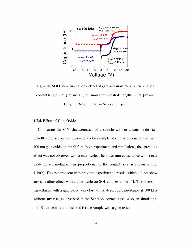
94
0
1
10
-20 -15 -10 -5 0 5 10 15 20
Ca
pa
citan
ce
(fF
)
Voltage (V)
f = 100 kHz
LGate= 50 µµµµm
LSub= 350 µµµµm
LGate= 50 µµµµm
LSub= 150 µµµµmLGate= 10 µµµµm
LSub= 350 µµµµm
CBOX for L= 350 µµµµm
Substrate width
CBOX L= 50 µµµµm
Contact size
Fig. 4.18. SOI C-V – simulation - effect of gate and substrate size. Simulation
contact length = 50 µm and 10 µm; simulation substrate lengths = 350 µm and
150 µm; Default width in Silvaco = 1 µm.
4.7.4. Effect of Gate Oxide
Comparing the C-V characteristics of a sample without a gate oxide (i.e.,
Schottky contact on the film) with another sample of similar dimensions but with
100 nm gate oxide on the Si film (both experiment and simulation), the spreading
effect was not observed with a gate oxide. The maximum capacitance with a gate
oxide in accumulation was proportional to the contact area as shown in Fig.
4.19(b). This is consistent with previous experimental results which did not show
any spreading effect with a gate oxide on SOI samples either [7]. The inversion
capacitance with a gate oxide was close to the depletion capacitance at 100 kHz
without any rise, as observed in the Schottky contact case. Also, in simulation,
the “S” shape was not observed for the sample with a gate oxide.

95
The experimental results for a thin film SOI with a 100 nm gate oxide was not
measureable and was not conclusive as shown in Fig. 4.19(a). Dry oxidation was
carried out at 1000°C and the sample was pulled out of the chamber at 700°C.
The measurement abnormalities are most probably due to the following reasons;
(a) oxygen vacancies being neutralized at such high temperature, resulting in part
of the sample turning back to p-type (one curve shows a p-type result), (b) some
part may be intrinsic hence a flat C-V plot is observed, and (c) the vacancies may
be present in patches which causes local variation of C-V between different
contacts. The dotted line in Fig. 4.19(a) is for the total calculated maximum
accumulated capacitance for series combination of CBOX and CGate-Ox for 1 µm
thick BOX and 100 nm thick gate oxide respectively.
mm9.0diaforvalueCalculate
pF20
96.21
1
56.219
1
1
C
1
C
1
1 C alExperiment
BOXOX
TOTAL
=
=
+
=
+
=
SIMULATION: (see Fig 4.19 (b) simulation plot with gate oxide)
For tOX = 100 nm and L = 50 µm => COX = 17.27 fF
For tBOX = 1 µm and L = 50 µm => CBOX = 1.73 fF
simulationforvalueCalculatedfF
CC BOXOX
57.1
73.1
1
27.17
11
111
C So TOTAL =
+
=
+
=
CTOTAL from simulation = 1.24 fF (3.7 V to 20 V) (see Fig. 4.19(b) simulation
plot with gate oxide)

96
The simulated value of the total capacitance (accumulation) with gate oxide is
close to the calculated value. It is slightly less due to smearing of accumulation
layer. There is no spreading effect with gate oxide.
10
100
-20 -15 -10 -5 0 5 10 15 20
AL contact
Cs1-GateOx
Cs2-GateOx
Cs3-GateOx
Cs4-GateOx
Cs5-GateOx
Ca
pa
citan
ce
(pF
)
Voltage (V)
f = 100 kHz
AL contactNo Gate Ox
tfilm = 145 nm
tBOX = 1 µµµµm
tGateOX = 100 nm
CTotal = 20pF
AL contactNo Gate Ox
1
10
-20 -15 -10 -5 0 5 10 15 20
Ca
pa
citan
ce
(fF
)
Voltage (V)
f = 100 kHz
With Gate Ox
tGate Ox = 100 nm
CTotal = 1.57 fF
CBOX for L= 50 µµµµm
CBOX for L= 350 µµµµm
Ca
pa
citan
ce
(fF
)
tfilm = 145 nm
tBOX = 1 µµµµm
(a) (b)
Fig. 4.19. SOI C-V - effect of gate oxide for thin film SOI (tfilm = 145 nm and
tBOX = 1 µm). (a) Experimental results are inconclusive, (b) simulation results -
no spreading.
4.7.5. Effect of Film Thickness
Spreading was observed for thin (tfilm = 145 nm) and thick (tfilm = 1.25 µm)
film SOI in both simulation and experiments, as shown in Fig. 4.20, but the “S”
shape was absent in thick film SOI. For the p-type film and n-type substrate
combination with the Al contact directly on the film an n-type C-V curve is
observed for both thick film and thin film SOI in both simulation and experiment.
But when the Al contact is placed over a gate oxide then for the same
combination of film and substrate doping the thin film SOI shows an n-type C-V

97
whereas the thick film SOI shows a p-type C-V in both simulation and
experiment. In thick films the film depletion layer may not touch the interface
thereby dominating the C-V behavior; as a result, a p-type C-V is observed with
gate oxide as the film is p-type. And for the same reason, the “S” shape is not
observed in thick film SOI samples.
The key to the “S” shape in thin film SOI is the complete inversion of the film
below the contact region due to the contact work function difference and the
creation of a discontinuity in the accumulated region by the depletion region at
low positive bias. In thick film SOI, the entire film, from the contact to the BOX
interface is not inverted, but only partially inverted by the contact work function
difference. As a result, in the positive bias region, the film/BOX interface in thick
film SOI wafer remains completely accumulated. This continuous sheet of holes
at the film/BOX interface allows the ac signal to spread at all positive biases and
the capacitance becomes instantly higher. For thick films the hysteresis effect is
also not observed (see Fig. 4.21).

98
Film= 1.25 µµµµm, BOX= 0.145 µµµµm
Film= 0.145 µµµµm, BOX= 1µµµµm
1
10
-20 -10 0 10 20
Ca
pa
citan
ce
(fF
)
Voltage (V)
f = 100 kHztGate=100nm
Gate Ox
No Gate Ox
No Gate Ox
Thin Film
Thin Film
Thick Film
Gate OxThick Film
Thick Film :
Thin Film :
Film= 1.25 µµµµm, BOX= 0.145µµµµm
Film= 0.145 µµµµm, BOX= 1µµµµm
10
100
1000
-20 -10 0 10 20
Cap
acitan
ce
(p
F)
Voltage (V)
f = 100 kHztGate=100nm
No Gate OxNo Gate OxThin FilmThick Film
Gate OxThick Film
Thick Film :
Thin Film :
(a) (b)
Fig. 4.20. Effect of film thickness (thick => film/BOX = 1.25/0.145 µm vs. thin
=> film/BOX = 0.145/1 µm) (a) simulation, (b) experiment. “S” shape is absent
in thick film SOI. In thin film SOI, n-type C-V for both with and without gate
oxide. But in thick film SOI, “without gate oxide” → n-type and “with gate
oxide” → p-type C-V.

99
101
102
103
-20 -10 0 10 20
Ca
pa
cita
nce
(p
F)
Voltage (V)
18 10-4 cm2
103 10-4 cm2
Series, 100kHz
tox = 0.145µµµµm
tFilm = 1.25µµµµm
Vg = -20V to +20V
Vg = +20V to -20V
Agate = 332 10-4 cm2
tFilm = 1.25 µµµµm
tox = 0.145µµµµm
1
10
-20 -10 0 10 20
Cap
acita
nce
(fF
)
Voltage (V)
LContact = 50 µµµµm
f = 100 kHz
Vg = -20V to +20V
Vg = +20V to -20V
(a) (b)
Fig. 4.21. Effect of sweep direction on thick film SOI for different contact sizes,
(a) experiment, and (b) simulation. Hysteresis effect is not observed in thick film
SOI.
4.7.6. Effect of Film Doping Concentration
To check the effect of film doping concentration on C-V characteristics of
HRSOI the substrate doping concentration was kept constant at ND = 1014 cm-3
and the film doping concentration was changed from NA = 5x1012 cm-3 to 5x10¹⁵
cm-3. Increasing the film doping concentration shifts the curve to the left with the
same slope, Fig. 4.22. An upward kink is observed near 0 V for very low film
doping concentration, for NA = 5x1012 cm-3. With increase in the film doping
concentration the region below the contact can no longer be easily inverted by the
Schottky contact as the hole barrier height is reduced, so even at lower positive
bias the film/box interface below the contact can easily go into accumulation
creating a continuous accumulation layer compared to lightly-doped films and

100
hence the “S” shape begins to shift towards left and the capacitance reaches the
spread value at lower positive bias and ultimately it vanishes.
1
10
-20 -15 -10 -5 0 5 10 15 20
Ca
pa
citan
ce
(fF
)
Voltage (V)
f = 100 kHz
Film - NA=1016 cm-3
5x1015 cm-3
1014 cm-3
5x1012 cm-3
Substrate
ND=1012 cm -3
Fig. 4.22. Simulated SOI C-V using Schottky contact – effect of change in film
doping concentration, tfilm=145 nm, tBOX = 1 µm.
4.7.7. Effect of Substrate Doping Concentration
To check the effect of substrate doping concentration on C-V characteristics of
HRSOI the film doping concentration was kept constant at NA = 1014 cm-3 and the
substrate doping concentration was changed from ND = 3x1011 cm-3 to 1012 cm-3.
When the substrate doping concentration reduces, the inversion capacitance
reduces, as the inversion layer becomes thicker and the depletion layer becomes
wider. The “S” shape is not affected as the film doping is kept constant but the
accumulation capacitance decreases with reduction in substrate doping
concentration due to smearing of the accumulation layer at low doping
concentration [135], as shown in Fig. 4.23.

101
1
10
-20 -15 -10 -5 0 5 10 15 20C
apa
citan
ce
(fF
)
Voltage (V)
f = 100 kHz
Sub - ND=3x1011 cm-3
1x1012 cm-3
7x1011 cm-3
Film - NA=1014 cm-3
Fig. 4.23. Simulated SOI C-V using Schottky contact - effect of change in
substrate doping concentration, tfilm=145 nm, tBOX = 1 µm..
4.7.8. Effect of Carrier Lifetime
The film lifetime affects the C-V characteristic of HRSOI in the accumulation
region, increasing the film electron and hole carrier lifetimes from τn/p = 10-7 s to
τn/p = 10-4 s increases the capacitance at a particular positive bias. But changing
the substrate carrier lifetimes does not have any significant impact on the C-V
plots, as shown in Fig. 4.24. The film carrier lifetime affects the lateral minority
carrier injection and recombination in the film. As the lifetime increases the
recombination rate decreases and the holes in the film cannot be neutralized faster
and the capacitance remains high for a particular bias. The carriers can spread to
greater distances compared to that at lower lifetimes (10-7 s).

102
1
10
-20 -15 -10 -5 0 5 10 15 20C
(fF
)Voltage (V)
f = 100 kHz
ττττSub/Film= 10-4 s
ττττFilm= 10-4 s
ττττSub= 10-7 s
ττττSub/Film= 10-7 s
ττττSub= 10-4 s
ττττFilm= 10-7 s
Fig. 4.24. Simulated SOI C-V using Schottky contact – effect of change in carrier
lifetime, , tfilm=145 nm, tBOX = 1 µm, NA,film = 1014 cm-3, ND,sub = 7x1011 cm-3.
4.7.9. Effect of Contact Work-function
The work-function of the source and substrate contacts affects the “S” shape in
the accumulation region during positive bias. In simulation, samples with high
hole barrier height contacts (WF = 3.4, 3.9, 4.08 eV) have the “S” shape and all
of them have almost the same C-V plot but for low hole barrier height contacts
(WF = 4.2, 4.8 eV) the “S” shape is not observed, it has a constant accumulation
capacitance and then falls to depletion capacitance near 0 V and then enters
inversion with a step, Fig. 4.25(a). The high hole barrier causes complete
inversion of the film below a certain positive bias and subsequent minority carrier
injection into the film. Due to the higher hole barrier height it is difficult for the
holes present in the other part of the film to leave causing hole accumulation and
the “S” shape in C-V as explained earlier. But for low hole barrier heights, the
film region below the contact cannot be completely inverted during positive bias

103
and does not create any interruption in the accumulation layer in the film. Hence
the ac signal can spread easily and the “S” shape is not observed.
The nature of the top film contact (Ohmic or Schottky) has a significant
impact on the C-V curve compared to the substrate contact. Similar “S” shaped
curves are observed when the substrate contact is Ohmic and the film contact is
Schottky, and when both substrate and the film contacts are Schottky (WF = 4.08
eV), Fig. 4.25(b). But when both the film and the substrate contacts are Ohmic
then the “S” shape is not observed in the positive bias region of the film contact,
but a constant accumulation capacitance is observed followed by the depletion
capacitance. The Ohmic contact prevents minority carrier injection and also it
does not create the inverted/depleted region below the contact interrupting the
film accumulation layer, as explained earlier. Now the entire film is accumulated
during all positive bias, the ac signal can spread easily immediately after 0V (in
accumulation) and the majority carries respond equally all along the film/BOX
interface leading to a higher capacitance (spread).

104
1
10
-20 -15 -10 -5 0 5 10 15 20
WF=3.4 eV
WF=3.9 eV
WF=4.08 eV
WF=4.2 eV
WF=4.8 eV
Ca
pa
citan
ce
(fF
)
Voltage (V)
f = 100 kHz
1
10
-20 -15 -10 -5 0 5 10 15 20
Ca
pa
citan
ce
(fF
)
Voltage (V)
f = 100 kHz
Source & SubOhmic
Source & SubSchottky
Source SchottkySub Ohmic
WF = 3.9 eV
(a) (b)
Fig. 4.25. Simulated HRSOI C-V - Effect of contact type (Ohmic/Schottky).
4.7.10. Effect of Radiation (Interface Charges and Interface Traps)
Interface traps change the slope of C-V plots and oxide charges shift the C-V
plots [11]. Radiation creates interface traps and oxide charges in an oxide and at
the oxide-silicon interface. Previous studies on radiation effect on MOS oxide
have shown that after radiation, if the sample is left as it is, the oxide
automatically heals due to room temperature annealing that heals the interface
traps and oxide charges [142, 143]. Annealing a sample at moderately high
temperature after radiation completely removes the interface traps and oxide
charges and the pre-radiation C-V curve is obtained [142, 143]. We tried to find
out how radiation affects the HRSOI C-V characteristics using a Schottky contact
when the film is p-type and the substrate is n-type. The samples were radiated
with different doses of Cobalt-60 radiation, such as, 25 krads and 100 krads. The
experimental results in Fig. 4.26(a) show the effect of radiation dose (0 rad, 25

105
krads, and 100 krads) on the C-V plot. Figure 4.26(b) shows the effect of room
temperature annealing on C-V plots for a particular radiation dose (100 krad).
And figure 4.26(c) shows the effect of annealing the sample at 400oC for 30 min
in forming gas ambient. The simulation results for various densities of interface
traps and oxide charges are shown in Fig. 4.26(d).
The concentration of interface traps and oxide charges increases with the
increase in radiation dose and they create both shift and change in the slope of C-
V plots [11]; similar effects are also observed but in a different manner as shown
in Fig. 4.26(a). As the radiation dose increases the slope of the C-V plot in the
accumulation region including the “S” shape becomes shallower indicating an
increase in interface traps, also a new phenomenon of a rising peak is observed at
VG → 0V in the positive bias region, as shown in Fig. 4.26(a). Comparing with
the simulation results in Fig. 4.26(d) this rise is mostly due to an increase in
interface trap densities. The effect of oxide charges can be seen by the left shift of
the depletion portion of the C-V plot in the negative bias region. Though this
effect could not be replicated in the 2D simulation, positive oxide charges are the
likely cause for the left shift, similar to the effect in a MOS capacitor. At higher
radiation dose (100 krad) the low frequency portion of the C-V plot is completely
flat. Also higher radiation dose widens the depletion portion compared to the pre
radiation case, most likely due to interface traps, which reduce the slope of the C-
V curve, hence the curve looks widened during depletion.
Room temperature annealing causes the interface traps to heal gradually with
time. Multiple measurements were taken at different time intervals such as 4, 29,

106
46 and 99 hours after radiating the sample at 100 krad. Figure 4.26(b) shows the
room temperature annealing effect in action. With time, the slope in the
accumulation region i.e., in positive gate bias, becomes steeper, the peak
observed near Vcontact = 0V gradually reduces, and the depletion portion, which
had shifted left, starts shifting towards right, i.e., the radiated C-V plot begins to
approach the pre radiation plot. The sample was annealed at 400ºC for 30 min in
forming gas to see if the interface tarps and oxide charges are completely
removed; and as expected, the C-V measurement after annealing showed a plot
very close to the original pre-radiation case, Fig. 4.26(c).

107
10-12
10-11
10-10
-20 -10 0 10 20
Ca
pa
cita
nce
(F
)
Voltage (V)
tox = 1µµµµm
tFilm = 0.145 µµµµm
ρρρρ = 18 kΩΩΩΩ.cmSeries, 100kHz
Effect of Radiation Dose
Area = 2 10-4 cm2
No Radiation
100 krad
25 krad
rad
10-12
10-11
10-10
-20 -10 0 10 20
No Rad
100 krad 4hr
100 krad 29hr
100 krad 46hr
100 krad 99hr
Ca
pacitan
ce (
F)
Voltage (V)
tox = 1µµµµm
tFilm = 0.145 µµµµm
ρρρρ = 18 kΩΩΩΩ .cmSeries, 100 kHz
Area = 2 10-4 cm2
Room Temp. Annealing
(a) (b)
10-12
10-11
10-10
-20 -10 0 10 20
No Rad100 krad 4hr
After annealCa
pa
citan
ce
(F
)
Voltage (V)
Annealing after radiation
Area = 2 10-4 cm2
Anneal @ 400C Forming gas20mins
1
10
-20 -15 -10 -5 0 5 10 15 20
Ca
pa
citan
ce
(fF
)
Voltage (V)
f = 100 kHz
IF Chg = 1011 cm-2
IF Chg = 1010 cm-2
No IF Chg/Trap
IF Trap = 1011 cm-2
IF Trap = 1011 cm-2
IF Chg = 1010 cm-2
(c) (d)
Fig. 4.26. HRSOI C~V - effect of radiation due to interface charges and interface
traps. Experimental C-V after Cobalt-60 radiation (a) effect of radiation dose, the
curves shift left and depletion region widens, (b) effect of room temperature
annealing, curve shifts towards the no radiation plot as the interface traps and
charges heal, (c) effect of annealing after radiation, and (d) simulation of interface
and oxide charges: substrate ND = 7x1011 cm-3, film NA = 1014 cm-3, substrate and
film (gate) contacts Schottky (WF = 4.08 eV), LGate =50µm, LSubstrate =350 µm,
tFilm =145 nm, tBOX =1 µm, tSub =100 µm.

108
4.7.11. Effect of Light, Temperature, and Annealing
Figure 4.27(a) and (b) show the effect of light and temperature respectively, as
the light intensity increases or the temperature increases (24°C to 300°C) the
spreading increases mainly due to more carrier generation and reduction in sheet
resistance. At very high temperatures it tends to act like a parallel plate capacitor.
Figure 4.27(c) shows the effect of annealing in forming gas at 450°C, 525°C and
550°C. Annealing temperature could not be increased beyond 560°C as it can
form aluminum-silicon eutectic. Spreading reduces with annealing.
10
100
-20 -10 0 10 20 30
DarkMidium intensityHigh Intensity
Ca
pa
citan
ce
(pF
)
Voltage (V)
f = 100 kHz
10
100
-20 -10 0 10 20 30
24C50C
100C150C200C
250C300C
Ca
pa
citan
ce
(pF
)
Voltage (V)
f = 100 kHz
(a) (b)
10
100
-20 -10 0 10 20 30
Anneal 450C
Anneal 525C
Anneal 550C
Ca
pa
citan
ce
(pF
)
Voltage (V)
f = 100 kHz
(c)
Fig. 4.27. Effect of light, temperature and annealing.

109
4.8. Conclusion
The C-V characteristics of HRSOI were studied in detail by experiments
and simulation with a metal contact directly on the film. Various factors affecting
the C-V characteristics were also studied, they are: frequency, size of the top film
contact, effect of the contact size and the substrate size, film thickness, film and
substrate doping concentrations, carrier lifetimes, contact work-function, and type
of film contact i.e. Schottky or Ohmic, radiation, temperature, light, and
annealing. Series C-V method with the bias applied to the substrate is preferable
for HRSOI for lower noise and more accurate measurement. The substrate
HRSOI doping type can undergo a reversal from p- to n-type at low substrate
doping concentration due to formation of oxygen thermal donors after annealing.
Samples with p-type films and n-type substrates with very low doping
concentrations (7x1011 cm-3 to 1012 cm-3) were studied.
The C-V plots showed spreading of capacitance following an “S” shape at
high frequency where the capacitance changes from a value proportional to the
contact area to a value 5 to 10 times larger. The spreading is mostly due to the
floating body and the contact being directly on the film and due to the RC
transmission line behavior of the film/BOX/substrate interface. The capacitance
spreading is not observed when there is a gate oxide. This shape is mainly due to
the Schottky contact and its work-function. The “S” shape was not observed for
Ohmic contacts and Schottky contacts with low hole barrier heights. It occurs due
to the depletion and inversion of the film below the contact at a particular positive
gate bias due to the large work-function difference between the p-type film and

110
the aluminum contact. The Schottky contact can supply minority carriers
(electrons) which respond to the ac signal and the capacitance is confined to the
contact area. The “S” shape does not occur for thick film SOI as the inversion
layer does not touch the film/BOX interface allowing a continuous accumulation
layer to be formed in the positive gate bias all along the BOX interface.
The RC transmission line behavior of the film and the substrate plays a
significant role in the bias spreading and the shape of the C-V characteristic. At
higher frequencies the ac signal flows very close to the contact due to the low-
pass filter nature of the RC circuit and spreads less into the other part of the film
giving smaller capacitances than at a lower frequency.
Radiation effects on the C-V plots were also studied. The C-V plot shifted
to more positive voltages at higher radiation doses and had shallower slopes due
to radiation induced interface traps and oxide charges. The radiated samples also
had an upward peak near zero bias, which is not observed in any other C-V plots;
most probably due to interface traps. Due to the room temperature annealing
effect a gradual change in the slope, reduction in the peak near zero bias, and shift
of the C-V plot towards the pre-radiation plot indicating healing of interface traps
were observed with time. When the sample was annealed at 400°C for 30 mins in
forming gas ambient the radiation induced damages were healed.

111
CHAPTER 5. CROSSTALK IN HIGH-RESISTIVITY SILICON WAFERS
– BULK AND SILICON-ON-INSULATOR
5.1. Introduction
Today’s IC chips are operating at ever higher speeds in the GHz range and
becoming smaller and more powerful with multiple functionalities being
integrated in a single chip. This integration of different circuits or systems such as
analog, digital and microwave on a single chip is called the System-on-Chip
(SOC) configuration, as shown in Fig. 5.1. The first true SOC appeared in a
Microma watch in 1974 when Peter Stoll integrated the LCD driver transistors as
well as the timing functions onto a single Intel 5810 CMOS chip [144, 145]. Ever
since, the SOC chips have become denser, faster and more powerful [146]. But
this complex integration of analog, digital and microwave systems and higher
operating frequency gave rise to another problem called crosstalk. While the
digital circuits run at a very high speed in the GHz range, the analog circuits are
very sensitive to any noise. At high frequencies some spurious signals from the
digital node can pass through the substrate and couple to the analog side and
disrupt the analog operation [17-19]. This is termed as crosstalk through the
substrate. Figure 5.2(a) illustrates an example of coupling mechanism between a
digital and an analog circuit present on the same substrate [147]. The digital
inverter generates noise which couples into the analog NMOS transistor.
SOI substrates were found to have lower substrate crosstalk than bulk
substrates of similar resistivity [20, 21]. High-resistivity silicon (HRS) wafers
minimize this coupling compared to low-resistivity substrates (LRS) and

112
specifically high-resistivity SOI wafers are found to have better cross talk
prevention capabilities than bulk Si of similar resistivity [22, 23]. This chapter
will focus on substrate coupling in HRSOI and effects of various factors, such as:
substrate resistivity, separation between devices, buried oxide (BOX) thickness,
radiation, temperature, annealing, light, and device types. And also various ways
to minimize substrate crosstalk will be discussed.
Fig. 5.1. Block diagram of a typical System-on-Chip configuration integrating
digital, analog, and RF systems in one chip [148].
5.2. What is Substrate Crosstalk – Mechanism and Factors Affecting It?
Substrate crosstalk can be defined as coupling of signal or noise through the
substrate between two devices or systems residing on the same substrate. When
we have both high speed digital circuit and sensitive analog circuits on the same
chip sharing the same substrate then during high frequency operation the

113
switching transients can couple from digital to analog circuit through the substrate
[149]. Substrate cross talk mechanism can be segregated into three parts:
generation, transmission and detection of substrate noise; and can be explained
with the help of Fig. 5.2(b).
(a)
(b)
Fig. 5.2. (a) An example of coupling mechanisms between a digital (noise source)
and analog (affected) circuit on the same substrate [147]. (b) Schematic of noise
injection, reception and substrate paths in CMOS technology [150].

114
There are different mechanisms by which noise can be injected into the
substrate [149]:
1. Capacitive coupling of voltage fluctuation at the drain and at metal
layers to the substrate through the source/substrate or drain/substrate
junction capacitors, in SOI it can couple through the BOX capacitor.
2. Another mechanism is by the impact ionization induced substrate
current. Impact ionization at the drain end of an NMOS creates hole
current in the substrate, PMOS also creates a similar substrate current
but it is much lower than NMOS and at the same time the capacitive
shielding by the n-well junction reduces it further, making its
contribution to the total substrate current insignificant. Hence the
substrate current is mainly considered to be due to NMOS and this can
couple to other devices through the substrate.
3. Noise injection by power supply lines connected to the substrate, e.g.,
digital ground.
The injected signal is transmitted through the substrate by its parallel RC
circuit as shown in Figs. 5.2(a, b). The injected signals can again couple to other
nodes (device drains and metal lines) by capacitive coupling.
The crosstalk is basically the transmission of a signal through an RC circuit
and hence is dependant on the frequency of the coupled signal as shown in Fig.
5.3. Below a certain frequency the substrate can block the coupling and beyond a
certain frequency, say ωt dependant on R and C of the substrate, as shown in Fig
5.2(b), the substrate can gradually become transparent to the noise signal and

115
coupling increases. The frequency dependence of crosstalk (measured by S21
parameter vs. frequency) in Fig. 5.3 indicates that at lower frequencies the
crosstalk increases with increase in frequency as the capacitive coupling
increases, at medium frequencies the substrate resistance begins to dominate as
the crosstalk is lower for high resistive substrates, and at very high frequencies the
capacitance of the silicon contributes [150].
Figure 5.4 shows the substrate coupling effect through various types of
substrates: bulk silicon in Fig. 5.4(a), epitaxial silicon in Fig. 5.4(b), and high
resistivity SOI in Fig. 5.4(c). In bulk silicon, the current lines indicating coupling
are near the surface and through the substrate, this can be reduced by using guard
rings. In epi silicon, substrate coupling increases as more current lines can pass
through the low resistive path of the heavily-doped epi layer. High-resistivity SOI
prevents substrate coupling to the maximum extent compared to all other
substrate types due to the presence of the buried oxide layer that isolates the
device layer from the substrate and the high resistivity of the substrate. SOI can
prevent coupling better than bulk silicon of similar resistivity and HRSOI is better
than LRSOI. The corresponding simulation results using Silvaco ATLAS Device
simulator are shown in Fig. 5.3, modeled after Raskin et al. [23]. The device cross
sections used in simulation are shown in Fig. 5.5. Two types of p-type substrates
were used, one with HRS substrate, ρsubstrate = 5000 Ω.cm (NA = 3x1012 cm-3) and
the other with LRS substrate, ρsubstrate = 20 Ω.cm (NA = 7x1014 cm-3). The two
devices were pn diodes with n+ doping concentration of ND = 1019 cm-3; and the
devices were 100 µm apart. For the epi substrate the p+ epi layer doping

116
concentration was NA = 1019 cm-3. The simulation results in Fig. 5.3 show that
among various substrate types, HRSOI has the least crosstalk for the same device
configuration.
It has been reported in prior studies that in SOI substrates crosstalk is affected
by various factors, such as: spacing between the devices (the noise injecting
source and the affected entity), the frequency of the signal, the buried oxide
thickness, substrate resistivity and the nature of the substrate/BOX interface.
-100
-80
-60
-40
-20
0
107 108 109 1010 1011 1012
Si Bulk 20 ohm.cm
SOI 20 ohm.cm
P+ Buried Layer Si Bulk
SOI FloatSub 20 ohm.cm
SOI FloatSub 5000 ohm.cm
SOI 5000 ohm.cm
S2
1 M
ag
nit
ud
e (
dB
)
Frequency (Hz)
Fig. 5.3. Simulation - substrate coupling through various substrate types. High-
resistivity SOI has the lowest substrate coupling.
(a) (b) (c)
Fig. 5.4. Substrate coupling through various substrate types. High-resistivity SOI
has the lowest substrate coupling compared to other substrates.

117
(a) (b) (c)
Fig. 5.5. Device cross sections using different substrate types with dimensions
used in simulation; (a) bulk silicon, (b) epi substrate, and (c) SOI substrate.
5.3. Crosstalk Measurement Procedure
Substrate crosstalk measurement involves very high frequencies microwave
measurements in the GHz frequency range. It is a two port measurement where
the input port is the noise injecting node and the output port is the device being
affected, and the main coupling medium is the substrate on which both the
devices are present. Coplanar waveguides (CPW) with 50 ohm characteristic
impedance (Z0 = 50 Ω) were used to transmit the high-frequency input signals to
the device under test (DUT) and to measure the output i.e. the coupled signal to
the output node. A Vector Network Analyzer (VNA) is the instrument to measure
crosstalk. Crosstalk measurement like any microwave measurement is a two step
process, first step is the calibration of the VNA and the second step is the actual
measurement of the device S-parameters. A brief discussion of CPW and S-
parameter are presented in the next subsections.
5.3.1. Coplanar Wave Guide (CPW)
The coplanar waveguide (CPW) was invented by C. P. Wen from RCA
Laboratory in 1969 [151]. The basic coplanar waveguide consists of a center

118
signal line with two ground lines on both sides separated by a narrow gap in a
GSG (Ground Signal Ground) configuration placed over a substrate which acts as
the dielectric (see Fig. 5.6). The original design assumed the adjacent ground strip
widths and the dielectric thickness to be infinite. In practice, the dielectric should
be thick enough so that the electromagnetic waves die out before they leave the
substrate, and the ground strips are of finite width. The dimensions of the center
strip, the gap between the signal and the ground lines, the thickness and the
permittivity of the substrate dielectric determine the effective dielectric constant
(εeff) and the characteristic impedance (Z0) of the CPW [152]. CPWs are most
suitable for low-loss high-frequency signal transmission, it can be used to transmit
signal with frequencies exceeding 100 GHz.
(a) (b)
Fig. 5.6. Coplanar waveguide (a) conventional (b) with finite conductor length.
5.3.2. S-Parameter
A microwave circuit with an input and output node can be represented by the
two-port network in Fig. 5.7(a). In this high frequency system a portion of the
source power is delivered to the load by means of transmission lines. Voltage,
current, and power can be considered to be in the form of waves traveling in both
directions along this transmission line. Due to mismatch between the source

119
impedance (ZS), characteristic impedance of transmission line (Z0) and output
impedances (ZL) a portion of the wave incident on the load will be reflected, it
then becomes incident on the source, and in turn re-reflects from the source (if ZS
≠ Z0), resulting in a standing wave on the line.
Scattering parameters, commonly called S-parameters, relate those waves
scattered or reflected from the network to those waves incident upon the network
[153]. S-parameters are important in microwave design because they are easier to
measure and work with at high frequencies than other kinds of parameters. They
are easier to understand because they are nothing but gains and reflection
coefficients as described in eqns. 5.7 to 5.10. S-parameters and distributed models
provide a means of measuring, describing, and characterizing circuit elements
when traditional lumped equivalent circuit models cannot predict circuit behavior
to the desired level of accuracy. They are used for the design of many products,
such as cellular telephones.
S-parameters are measured by an instrument called Vector Network Analyzer
(VNA). They are usually measured with the device embedded between a 50 Ω
load and source, and there is very little chance for oscillations to occur.
Generalized scattering parameters have been defined by Kurokawa [154]. The
wave functions used to define S-parameters are shown in Fig. 5.7(a). The S-
parameters describe the interrelationships between the normalized complex
voltage waves incident on (ai) and reflected from (bi) the ith
port of the network. a1
and a2 are incident waves and b1 and b2 are reflected waves at port 1 and 2
respectively.

120
ZS
ZL
Two-portnetwork
a1
b1
a2
b2
VS ~
(a)
S21 = (b2/a1)|a2=0
(b)
Fig. 5.7. (a) Two-port network with source impedance ZS and output load
impedance ZL showing incident waves (a1, a2) and reflected waves (b1, b2) used in
S-parameter definitions, (b) S21 parameter of a two port network.
The independent variables a1 and a2, the normalized incident voltages, are
expressed as [153, 155]:
0
1i
00
011
1Z
V
Z
1portonincidentwaveVoltage
Z2
ZIVa ==
+= (5.1)
0
2i
00
022
2Z
V
Z
2portonincidentwaveVoltage
Z2
ZIVa ==
+= (5.2)
The dependent variables b1 and b2, the normalized reflected voltages, are
expressed as [153, 155]:
0
1r
00
011
1Z
V
Z
1portfromincidentwaveVoltage
Z2
ZIVb ==
−= (5.3)

121
0
2r
00
022
2Z
V
Z
2portfromreflectedwaveVoltage
Z2
ZIVb ==
−= (5.4)
The linear equations describing the two-port network are [153, 155]:
2121111 aSaSb += (5.5)
2221212 aSaSb += (5.6)
The S-parameters S11, S12, S21, and S22 are defined as [153, 155]:
0a1
1
11
2
a
b
Incident
flectedReS
=
== =
0)=a setsZ=(Z load matched
aby terminated port output the
withtcoefficien reflection Input
20L
(5.7)
0a2
2
22
1
a
b
Incident
flectedReS
=
== =
0)=V setsZ=(Z load matched
aby terminated port input the
withtcoefficien reflection Output
S0S
(5.8)
0a1
2
21
2
a
b
Incident
dTransmitteS
=
== =
load matched a in terminated
port output the withgain
)(insertion ontransmissi Forward
(5.9)
0a2
1
12
1
a
b
Incident
dTransmitteS
=
== =
load matched a in terminated
port input the withgain
)(insertion ontransmissi Reverse
(5.10)
S21 (forward transmission coefficient) as shown in Fig. 5.7(b) is used to
measure the crosstalk. S-parameters are measured in dB, the lower the value of
S21 i.e., the more negative S21 in dB is the lower is the crosstalk. Figure 5.8
illustrates the S-parameters along with the incident and reflected voltage waves.

122
Fig. 5.8. Pictorial view of S-parameters.
5.4. VNA Calibration Techniques
Figure 5.9 shows the block diagram of a Vector Network Analyzer (VNA).
The RF source at the top provides the required stimulus to the device-under-test
(DUT). A forward/reverse switch directs the RF energy to either DUT port. The
test set uses directional couplers or bridges to pick up the forward and reverse
waves traveling to and from each port, and down-converts these signals to four
“IF” sections. Each “IF” section filters, amplifies, and digitizes the signals for
further digital processing and display [156].

123
Fig. 5.9. Main hardware blocks of a Vector Network Analyzer (VNA) [156].
A VNA measures vector ratios of reflected or transmitted energy to energy
incident upon the DUT. As a stimulus-response measurement, a VNA
measurement determines the properties of devices rather than the properties of
signals [156]. A significant challenge in stimulus-response measurements is
defining exactly where the measurement system ends and the DUT begins. In on-
wafer VNA measurements this boundary is known as the “reference plane” of the
measurement and is often located at the probe tips, as shown in Fig 5.10(a).
Ideally the system will measure the characteristics of whatever is connected to the
measurement reference plane.
VNA calibration is an essential step in the measurement process that removes
the parasitic capacitances, inductances and resistances due to the VNA, cables,
probe station, probes and the probe pads. Without calibration, the measurement

124
does not provide the correct S-parameters only due to the actual devices. Figure
5.10(b) illustrates the block diagram of Thru-Reflect-Line (TRL) calibration
process. During calibration the VNA measures and stores the contribution due to
the error boxes and removes these errors from the actual measurements to
calculate the actual S-parameters due to the DUT only.
VNA & Cabling Errors
Probe Errors DUT Probe ErrorsVNA & Cabling
Errors
On Wafer reference plane
VNA & Cabling Errors
Probe Errors DUT Probe ErrorsVNA & Cabling
Errors
On Wafer reference plane
(a)
(b)
Fig. 5.10. Calibration removes the errors due to parasitic elements (VNA, probes,
probe station, and cables) from the actual measurement and helps calculate the
correct S-parameters due to the DUT only [155].
5.4.1. Calibration Options and Standards
The different calibration options such as un-corrected measurement, response
calibration and full two port calibration methods are described in table 5.1.

125
Table 5.1 Calibration options [156].
OPTION ILLUSTRATION
Un-corrected measurement:
A VNA will measure uncorrected S-parameters if not calibrated.
Uncorrected measurements are rarely used. Poor accuracy but fast.
Response calibration:
A “response” calibration is simply a vector magnitude and phase normalization of a transmission or reflection measurement.
Used only at low frequencies. Requires only one standard and low accuracy.
DUT
THRU
Full two port calibration:
This method is typically a full calibration of all the error parameters; is used as a reference or to assure the highest accuracy.
Removes following errors – Directivity – Source/load match – Reflection/transmission tracking – Crosstalk
Requires up to 7 standards.
There are two types of VNA calibration standards, they are: (a) On-wafer, and
(b) Off-wafer VNA calibration. Off-wafer calibration standard uses an Impedance
Standard Substrate (ISS) with predefined elements to calibrate the VNA. But as it
is not done on the same substrate as the DUT there are errors in the calibration
process which become significant during high frequency measurements.

126
On-wafer calibration standard uses the calibration structures fabricated on
the same substrate as the DUT and hence are more accurate at high frequencies
exceeding 20 GHz. On-wafer calibration standards most often are precision thin-
film resistors, short-circuit connections, and 50 ohm transmission lines fabricated
either on the wafer containing the DUT or on a separate Impedance Standard
Substrate (ISS) [156]. Open circuit standards are normally implemented by
raising the probe in air above the wafer by 250 µm or more. A true 'thru' standard
does not exist for on-wafer measurements since probes cannot directly connect to
each other and must instead use a very short transmission line as a thru standard.
A thru line standard may be referred to either with the label of thru or line.
The various VNA calibration techniques are:
• Thru-Reflect-Match (LRM)
• Thru-Reflect-Reflect-Match (LRRM)
• Thru-Reflect-Line (TRL or LRL)
• Short-Open-Load-Thru (SOLT)
• Short-Open-Load-Reciprocal (SOLR)
We will discuss two popular characterization techniques, SOLT and TRL
techniques.
5.4.2. SOLT (SHORT-OPEN-LOAD-THRU) Calibration Technique
Traditional full two port calibration typically utilizes three impedance and one
transmission standards to define the calibrated reference plane. These standards,
typically a SHORT, OPEN, LOAD, and THRU make up the SOLT calibration
kit. This is the most commonly used calibration technique available on every

127
commercially available VNA. SOLT calibration technique uses off-wafer
calibration standard on an Impedance Standard Substrate (ISS) available in the
calibration kit. This calibration is the combination of two one-port SHORT-
OPEN-LOAD calibrations with additional measurements of a THRU standard to
complete the two-port calibration. All of the standards must be fully known and
specified [156].
The SOLT standards are reasonably well modeled with simple lumped
elements: open-circuit has capacitance, short-circuit has inductance, load has
inductance, and thru has delay (and loss). Often the open-circuit capacitance will
have a negative value since the probe lifted in air has less tip loading than when it
is in contact with a wafer. The SOLT calibration method is shown in Fig. 5.11.
(a) (b)
(c) (d)
Fig. 5.11. SOLT calibration using an Impedance Standard Substrate (ISS). The
calibration steps are (a) SHORT, (b) OPEN, (c) LOAD, and (d) THRU.

128
Precautions and Source of errors in SOLT calibration [156]:
• Improper probe placement introduces error hence all standards must be
accurately contacted physically, since the inductances are very
dependent on probe placement on the standard.
• Calibration coefficients must be correctly entered into the VNA to be
useful because improper cal-kit entry is one of the largest sources of
error in Off-wafer VNA measurements.
• Another common source of error is to forget to enter the delay of the
THRU line standard. A 1 ps THRU is normally used with the standard
probe pitch ISS versions (PNs 101-190 and 103-726) while a 4 ps
THRU is used with the wide probe pitch ISS versions (PNs 106-682
and 106-683). When using long THRU lines such as for Pyramid
probes it is important to use an accurate delay value and to provide an
accurate loss value.
5.4.3. TRL (THRU REFLECT LINE) Calibration Technique
TRL (THRU-REFLECT-LINE) calibration was proposed by Engen and Hoer
in 1979 [157]. The TRL calibration method requires three standards, they are: a
THRU connection, a high Reflection connected to each port, and a LINE
connected between the test ports, as shown in Fig. 5.12. This technique is realized
on the same wafer as the DUT using transmission line as the standard instead of
any external prefabricated discrete impedance standards [158]. It results in the
same 12 port error correction model as the other calibration methods. Only one
well-defined standard is required in the TRL calibration process, compared to

129
minimum of three precisely-known standards required for the conventional FULL
2-PORT method.
The three basic steps in TRL calibration are [158]:
• THRU - connection of port 1 and port 2 directly or with a short length
of transmission line.
• REFLECT - connect identical one-port high reflection coefficient
devices to each port, either OPEN or SHORT can be used for this.
• LINE - insert a short length of transmission line between port 1 and 2
(different line lengths are required for the THRU and LINE). Different
line lengths are used to calibrate for individual frequency ranges.
(a) (b) (c)
(d)
Fig. 5.12. On-wafer multi line TRL calibration technique using a CPW with Z0 =
50 Ω. The calibration steps are (a) THRU, (b) REFLECT (OEPN or SHORT), (c)
LINEs (multiple lines of different lengths for corresponding frequency ranges).

130
For TRL calibration, the calibration standards need to be prepared meeting the
following requirements [158, 159]:
• THRU (zero-length, or non-zero-length through)
o Zero-length THRU
S21 and S12 are defined as equal to 1. Typically used to
set the reference plane.
S11 and S22 are defined as equal to zero. A zero-length
THRU has no loss and has no characteristic impedance.
o Non-zero-length THRU
Z0 of the THRU and LINEs must be the same. When the
Z0 of the THRU and LINE are not the same, the average
impedance is used. S11 and S22 of the LINE are also
defined to be zero. With this assumption, the system
impedance is set to the characteristic impedance of the
LINE. If the Z0 is known but not the desired value, the
impedance of the LINE can be specified when defining
the calibration standards.
Attenuation need not be known.
Accurate electrical length must be known to set the
reference plane.
Insertion phase or electrical length must be specified if
the THRU is used to set the reference plane. If a non-
zero-length THRU is used but specified to have zero

131
delay, the reference plane will be established in the
middle of the THRU.
• REFLECT (SHORT, or OPEN termination)
o Any unknown highly reflective termination may be used as the
REFLECT (either OPEN or SHORT). Reflection coefficient
magnitude (optimally 1.0) need not be known.
o Phase of the reflection coefficient must be specified within 1/4
wavelength or +/-90 degrees.
o Must be the same reflection coefficient on all ports.
o May be used to set the reference plane if the phase response of
the REFLECT is well-known and specified.
• LINE (transmission line)
o Z0 of the LINE establishes the reference impedance after error
correction is applied.
o Electrical length need only be specified within 1/4 wavelength.
o Cannot be the same length as the THRU. Difference between
the THRU and LINEs must be between 20 degrees and 160
degrees.
o Optimal line length is 1/4 wavelength or 90 degrees relative to
the THRU at the center frequency.
o Usable bandwidth for a single LINE standard is 8:1 (frequency
span : start frequency).
o Attenuation need not be known.

132
o Multiple THRU/LINE pairs (Z0 assumed identical) can be used
to extend the bandwidth to the extent transmission lines are
realizable.
• MATCH (load termination, additional step for TRM/LRM method)
o Must be the same Z0 on all ports. Z0 = 50 Ω is preferred.
o Z0 of the MATCH standard establishes the reference impedance
of the measurement.
5.5. Design of 50 ΩΩΩΩ CPW, TRL LINE Standards, and Mask
The design section is divided into three parts to design the calibration
standards and the mask required for device fabrication. The design steps are:
• Design a CPW with 50 Ω characteristic impedance to transmit and
measure microwave signals to and from the DUT.
• Design of various line lengths required for the “LINE” standard of the
TRL calibration technique.
• Design of the photolithography mask needed for device fabrication.
5.5.1. Design of 50 ΩΩΩΩ Characteristic Impedance CPW
The main goal of the overall design stage is to design a CPW with constant
characteristic impedance of 50 Ω within 1 to 100 GHz frequency range in order to
transmit microwave signal with minimal loss to the DUT and to measure the
coupled signal. HFSSTM, a 3D microwave design tool by Ansoft®, was chosen to
design the CPW.

133
HFSS™ is an industry-standard simulation tool from Ansys Corporation for
3D full-wave electromagnetic field simulation [160]. The acronym HFSS stands
for High Frequency Structural Simulator. HFSSTM provides E- and H-fields,
currents, S-parameters and near and far radiated field results. It is a high-
performance interactive software package that uses finite element analysis (FEA)
to solve three-dimensional (3D) electric, magnetostatic, eddy current and transient
problems.
The CPW design was carried out using Design of Experiment (DOE)
techniques to achieve the required specification using scientific methods in
minimum number of simulation runs and least amount of time [161]. Latin
Hypercube model of Space Filling Design in JMPTM was used as a design tool.
The response variables (design output variables) are the average characteristic
impedance (Z0) of the CPW and the standard deviation of Z0 within the frequency
range 1 GHz to 100 GHz. The target value of Z0 is 50 Ω with upper and lower
specification limits of 49.5 Ω ≤ Z0 ≥ 50 Ω; in the mentioned frequency range. The
characteristic impedance measured between two ports in HFSSTM should be the
same. Z0 is the output of each successful HFSSTM simulation run; it is available
under “Results →→→→ Solution Data →→→→ Z0” in HFSSTM. Figure 5.13 shows the various
factors involved in CPW design on an SOI substrate.

134
Fig. 5.13. Coplanar waveguide structure used in HFSSTM simulation.
The actual design factors are length, width and thickness of the signal and
ground lines, the gap between them, and the frequency of the applied TEM.
Wave-port is only a HFSSTM simulation requirement, not a physical parameter.
But the dimension (height and width) of the wave-port impacts the simulation
result. Too small a size gives a low value of Z0 and too large a size gives a large
value due to various other modes. So this is a nuisance factor which is known and
controllable. During the simulation the first step was to find out an optimal size of
the wave-port and use that size to vary the actual design factors to achieve Z0 =
50 Ω. As a rule of thumb the height and width of the wave-port should be less
than half the wavelength (λ/2) of the applied Transverse Electromagnetic wave
(TEM). The wave-port size was fixed at height = 500 µm and width = 300 µm.
The substrate width and length were held constant at 1 mm for all simulation. The
thickness of ground and signal line was 1 µm. The simulations were carried out
for ten frequency steps: f (in GHz) = 1, 11, 21, 31, 41, 51, 61, 71, 81, 91, 101.

135
The oxide material was SiO2 and the CPW lines were of aluminum. Figure 5.14
shows the cause-effect diagram of the various factors affecting the characteristic
impedance of the CPW during HFSSTM simulation.
Characteristic Impedance
= 50 ΩΩΩΩ
Uncontrollable Factors
Controllable Design Factors
Held-constant Factors
Nuisance Factors
(Controllable)
Line Width - Ground
Gap
Line Width - Signal
Line thickness
Line Material
Oxide Material
Substrate Material
Substrate Thickness
Oxide Thickness
Line Length
Wave Port Width
Wave Port Height
Simulation Tool
Frequency
Fig. 5.14. Cause-effect diagram of various factors affecting CPW design.
The HFSSTM simulation structure is shown in Fig. 5.15. Because of symmetry
of the CPW structure only half the structure was simulated from time, computer
resource and mesh point-of-view. The ground line was of actual width and the
signal line was half the size. With this half structure the simulated Z0 was 100 Ω
which is equivalent to 50 Ω for a full structure. It was observed that average Z0
increases as the gap between the lines increases and it decreases as the width of
the signal or the ground line increases. Also, any changes to the width of the
signal line have greater influence on the value of average Z0 than changes to the

136
width of the ground line. Multiple sets of line widths (ground and signal lines)
and the gap between them result in average Z0 = 50 Ω. The final dimensions of
the CPW was decided to be, gap = 40 µm, width of signal line = 78 µm and width
of ground line = 160 µm to get an Average Z0 = 50 Ω in 1 to 100 GHz frequency
range with minimum standard deviation.
Si Substra
te
Oxid
e
Gro
undSignal
Si Substra
te
Oxid
e
Gro
undSignal
Fig. 5.15. HFSSTM design schematic of the CPW using half-structure.
5.5.2. Design of the “Line” standards of TRL Calibration
The other design goal was to design transmission lines of appropriate lengths
for various frequency ranges required for the “Line” standards of TRL calibration
technique. We are trying to measure crosstalk over a large frequency range from 1
GHz to 100 GHz; a single line will not correctly calibrate all parasitics at all

137
frequencies as the capacitance and inductances are frequency dependent. Hence
lines with different lengths had to be designed to correctly calibrate the VNA at
different frequencies. The effective permittivity of the structure εeff was calculated
from HFSSTM simulations corresponding to the CPW dimensions that resulted in
50 Ω characteristics impedance, and this εeff value was used to calculate the line
lengths for calibration. Figure 5.16 shows the relation between a particular
frequency range and the corresponding line lengths, where f0 is the center
frequency at λ/4 for electrical length θ = 90o; λ is the wavelength of a particular
frequency for which the line length is designed. A line designed for a particular f0
can calibrate up to ±0.9f0 (i.e. 90% of the center frequency). Equation 5.11 shows
the relationship between two frequencies on both sides of f0. If we start at 1 GHz
frequency, then the first f0 = 1.4 GHz and it can calibrate between 1 and 1.8 GHz.
Similarly other f0 can be calculated using Eq. 5.11. The line length for that
particular f0 is calculated using eqn. 5.12; where, l = length of the calibration line
for a particular frequency range corresponding to a particular f0. The range of
frequencies that are calibrated using each f0 and the corresponding line lengths
calculated using eqns. 5.11 and 5.12 [155] are shown in Table 5.2.
8.164
116
f
f
2
1
2
1 ===θ
θ (5.11)
meterinf4
10x3l
eff
8
ε= (5.12)

138
1 1.8 3.24 5.83 10.5 18.9
1.4 f0 = 2.52 4.54 14.7 8.17
Freq in GHz
0 64 90 116 180
0.9f0
f0
Electrical length (θ)θ)θ)θ) in Degrees
Fig. 5.16. Relationship between frequency and electrical length of a transmission
line used to design the “Line” standards of the On-wafer TRL calibration kit.
Table 5.2 Line lengths for various frequency ranges used in the “Line” standards
of On-wafer TRL calibration.
f0 GHz
(HFSS) εεεεeff
(HFSS)
LINE LENGTH
(µµµµm)
FREQUENCY
RANGE (GHz)
1.4 6.7 20696 1 - 1.8
2.52 6.7 11498 1.8 – 3.24
4.535 6.6 6437 3.24 – 5.83
8.165 6.4 3631 5.83 – 10.5
14.7 6.41 2015 10.5 – 18.9
26.45 6.37 1123 18.9 – 34.0
47.6 6.38 624 34.0 – 61.2
85.7 6.44 345 61.2 – 110.2
5.5.3. Mask Design for Fabrication
The last step of the design phase was to design the mask to fabricate the
devices and calibration standards on the wafer. AutodeskTM software was used for
mask design. The CPW has three lines in ground-signal-ground configuration, the

139
designed dimensions to have 50 Ω characteristic impedance in 1 GHz to 100 GHz
frequency range are: width of ground lines = 160 µm, width of the signal line =
78 µm, and the gap between the ground and the signal lines = 40 µm. The mask
dimensions of the CPW were drawn with a bias of 1 µm to achieve the designed
dimensions taking into account the processing anomalies. Figure 5.17 (a) shows
the mask layout with the actual device measurement section inside the dotted
square and the TRL calibration section (rest of the mask), one DUT unit in Fig.
5.17(b), and the mask dimensions in a tabular form in Fig. 5.17(c).
There are six different device arrangements with spacing between the devices
varying from 50 µm to 600 µm as shown in Fig. 5.17(a). The calibration section
of the mask has the THRU, REFLECT, and LINE connections. In “Line”
calibration the ports are connected by a 50 Ω transmission line with varying
lengths to calibrate at different frequencies as shown in table 5.2. The mask was
printed on a 5''x5''x0.090'' Sodalime glass substrate with chrome drawn polygons.

140
Fig. 5.17. (a) Mask layout with TRL calibration kit and actual device for
measurement, (b) mask dimensions of the CPW with two devices (Schottky
diodes), and (c) table with the actual designed dimensions and the corresponding
mask dimensions with bias.
5.6. Device Fabrication
The Schottky diodes (50 µm X 50 µm) and the on-wafer TRL VNA calibration
kit as shown in the mask layout in Fig. 5.17 were fabricated on SOI wafers with
different substrate resistivities, buried oxide thicknesses, and film thicknesses.
The lines and the devices were 1 µm thick aluminum contacts fabricated by
OPEN THRU SHORT L = 345u L = 624u L = 1123 u L = 2015 u
L = 3631 u L = 6437 u
L = 11498 u
L = 20696 u
d = 151u
d = 101u
d = 51u
d = 301u
d = 251u
d = 201u
d = 601u
d = 501u
d = 401u
OPEN THRU SHORT L = 345u L = 624u L = 1123 u L = 2015 u
L = 3631 u L = 6437 u
L = 11498 u
L = 20696 u
d = 151u
d = 101u
d = 51u
d = 301u
d = 251u
d = 201u
d = 601u
d = 501u
d = 401u
Measurement
Port 1 Port 2
ACTUAL
(µµµµm)
MASK
(µµµµm)
WidthGround 160 159
WidthSignal 78 77
Gap 40 41
Device 50 x 50 49 x 49
(a)
(b) (c)

141
evaporating aluminum directly on the silicon film and annealing at 400 ºC for 30
mins in forming gas ambient to form better contacts. The detailed processing
steps are described in Fig. 5.18.
Fig. 5.18. Processing steps for On-wafer TRL calibration kit and crosstalk
measurement units.
7µm PR
Si Wafer
(Step 6)
Dark field Mask
(Step 8)
(Step 14)
1µm AL
Si Wafer
7µm PR
(Step 15)
Si Wafer
1µm AL
1. Tools – Spinner, EVG620(Photo-lithography), Torr-Vac/Lesker 3(metal deposition), Furnace
(anneal).
2. Chemicals BOE (20:1), AZ400T, MIF300 (developer), AZ4620 (Photo-resist)
3. Break the wafer into the required size and then clean both sides by putting in AZ400T
for 10 mins heated at 160ºC. Rinse thoroughly in DI water and dry completely.
4. Dehydration bake at 120ºC for 15 min (to remove moisture).
5. Spin coat HMDS (transparent liquid) at 4000 rpm for 50 sec.
6. Put AZ4620 and spin at 3000 rpm for 40 sec (7µµµµm thick PR coating).
7. Soft bake (only when ready for Metal) at 85ºC/30 min slowly to
have 90 deg step coverage else edges will be slanted.
8. Using EVG620 expose for a dose ~ 500mj/cm2.
9. Develop using MIF 300 for ~ 5 - 6 min.
10. Rinse with DI water, Dry and inspect under the microscope to check the
sharpness of the edges. If not sharp then repeat steps 3 to 6.
11. Bake at 85ºC for 30 min, makes smooth profile, removes solvent and makes
the resist stick to the surface thoroughly so that acid won’t etch it.
12. Etch native oxide by first putting the wafer in BOE for 15 sec, then put it in
DI water for 1 min and then rinse thoroughly in DI water and dry.
13. Deposit metal, AL- 10,000 Ao using Lesker 3 evaporator.
14. Liftoff the unexposed layer (to bring out the contacts) using AZ400T (at 200ºC, set heater temp
to 200C). Heat the hot plate to 200C – Put the Beaker with 400T – Put the wafer in 400T – Keep it
on the hot plate for 10 min – put in the ultrasonic vibrator for 5 min – check for metal coming out.
Make sure no water mixes with AZ400T. Removal takes around 10 to 15 mins.
15. Rinse thoroughly in DI water and dry.
16. Check under microscope for sharpness of edges.
17. Anneal the devices in a furnace at 400ºC/30 min to make better contacts.
Processing Steps to fabricate CPW – 1µµµµm thick AL lines (Lift Off Process – Dark field Mask)
(Step 9)
Si Wafer
7µm PR

142
5.7. Measurement
Microwave measurements were taken using an HP8500 VNA (Vector Network
Analyzer) and the pico-probe station shown in Fig. 5.19. The probe station has
two pico-probes, one for the input port and the other for the output port with three
pins on each in ground-signal-ground configuration with 150 µm pitch between
the probes. First the VNA calibration step was performed and then the
measurement using the WinCal software. In “THRU” calibration connection,
port1 and port2 are connected directly and it measures the transmission
coefficients. The “REFLECT” calibration has the OPEN and SHORT connections
of the probe pads; it measures the reflection coefficients with large load. Open
configuration was used for reflect calibration. The measurements were carried
out within 1 to 18.9 GHz frequency.
(a) (b)
Fig. 5.19. Microwave measurement unit (a) HP8500 VNA (right) with Pico probe
station (left), and (b) the probes with the sample.

143
5.8. Simulation Setup
Crosstalk was simulated using Silvaco ATLAS device simulator. Crosstalk
was modeled using S-parameter simulation using the syntax
LOG OUTF=soi_S21_HeavySub_tox0p95.log MASTER GAINS S.PARAMS
INPORT=source OUTPORT=drain WIDTH=100
SOLVE ac freq=1 fstep=10 mult.f nfsteps=4 name=source
SOLVE ac freq=1e6 fstep=2 mult.f nfsteps=25 name=source
5.9. Analysis of Experimental and Simulation Results
Fig. 5.20. Lumped element equivalent circuit model describing crosstalk in SOI
substrate [23].
Substrate coupling in SOI can be modeled using a combination of resistors and
capacitors as shown in Fig. 5.20 [23]. “1” is the input noise injecting node and “2”
is the disturbed node. CBOX is the capacitance of the buried oxide, Ccp and Rcp are
the coupling capacitors and resistors through the substrate between device 1 and
2. R1 and C1 are the coupling capacitor and resistor between the bottom of the
BOX and the back substrate contact. The coupling though the Si film is neglected

144
as the film is very thin with high sheet resistance. The resistors and capacitors in
Fig. 5.20 are the main elements that affect the coupling. At frequencies above a
few hundred MHz the BOX capacitor CBOX offers negligible impedance and the
crosstalk is limited almost exclusively by the parallel combination of effective
substrate resistance Rcp and capacitance Ccp [23]. The resistivity of the silicon
handle wafer therefore becomes significant. If a high-resistivity silicon substrate
(HRS) is employed, cross-talk will be controlled by Ccp and should exhibit a 20
dB/decade frequency dependence. To understand the crosstalk effect on HRSOI,
various factors influencing these components and thereby the coupling were
studied. The substrate resistivities mentioned in all experimental results were
supplied by the wafer manufacturer.
To understand the factors affecting substrate crosstalk S21 parameter between
two Schottky diodes on various SOI substrates with varying substrate resistivities
were measured using the measurement procedure described earlier. The effects of
various factors were studied, such as: the spacing between the devices, substrate
resistivity, oxide thickness, interface charges/traps i.e., effect of radiation,
temperature, and light.
5.9.1. Effects of Device Spacing
Previous studies have shown that coupling through the substrate is related to
the spacing between the devices [23]. In HRS substrates the crosstalk reduces as
distance between the devices increases [19]. In order to understand the impact of
spacing on HRSOI we had devices with varying spacing between them as shown
in the mask layout in Fig. 5.17(a). The device separations were d = 50 µm, 100

145
µm, 150 µm, 200 µm, 250 µm, 300 µm, 400 µm, 500 µm, and 600 µm. The
experimental results for effect of device separation for two different substrates
with varying resistivity, BOX/film thickness are shown in Figs. 5.21(a, b) and the
corresponding simulation results are shown in Fig. 5.21(c). The wafer parameters
are given in Fig. 5.21(a, b). Both experimental and simulation results clearly show
that the substrate coupling reduces as the separation between the devices
increases. The total resistance between the devices increases as the separation
increases which reduces the signal that can couple from one point to the other.

146
-80
-60
-40
-20
109 1010
d=50u
d=100u
d=150u
d=200u
d=300u
d=400u
d=500u
d=600u
S21 M
ag
nitu
de (
dB
)
Frequency (Hz)
tBOX = 0.145µµµµm
tFilm = 1 µµµµm
ρρρρ = 1200 ΩΩΩΩ.cm50µm
600µm
-80
-70
-60
-50
-40
-30
-20
109 1010
d=50u
d=100u
d=150u
d=200u
d=300u
d=400u
d=500u
d=600u
S2
1 M
agn
itud
e (
dB
)
Frequency (Hz)
tBOX = 0.145µµµµm
tFilm = 1.25 µµµµm
ρρρρ = 33000 ΩΩΩΩ.cm50µm
600µm
(a) (b)
-100
-80
-60
-40
-20
0
107 108 109 1010 1011 1012
d=10um
d=20um
d=40um
d=70um
d=150um
d=200um
d=100um
S2
1 M
agn
itu
de (
dB
)
Frequency (Hz)
10 µµµµm
200 µµµµm
ρρρρ = 5000 ΩΩΩΩ-cm
tOX = 0.4 µµµµm
Nox = 0
Nit = 0
(c)
Fig. 5.21. Effect of device separation on crosstalk. Crosstalk (S21) reduces as the
separation between the devices increases in both experiments (from 50 µm to 600
µm) and simulations (10 µm to 200 µm). Experimental results for (a) ρsubstrate
=1200 Ω.cm, tBOX = 1 µm, tFilm=145 nm, and (b) ρsubstrate = 33 kΩ.cm, tBOX = 145
nm, tFilm=1.25 µm. (c) Simulation results for ρsubstrate = 5000 Ω.cm.

147
5.9.2. Effects of Substrate Resistivity
Figure 5.21 shows the effect of substrate resistivity on crosstalk. As the
substrate resistivity increases the coupling resistance RCP between the devices also
increases which lowers the coupling through the substrate. The experimental
results also point to a fact that after a certain resistivity the crosstalk does not
reduce significantly with further increase in substrate resistivity. Crosstalk
reduces significantly from ρsubstrate = 10 Ω.cm to 1.2 kΩ.cm, but the reduction is
not significant from 1.2 kΩ.cm to 33 kΩ.cm. The simulation results in Fig. 5.3
also show similar reduction in crosstalk from LRS (20 Ω.cm) to HRS (5000
Ω.cm) SOI. But for high frequencies above 10 GHz the substrate resistivity has
little effect in preventing crosstalk.
-80
-70
-60
-50
-40
-30
-20
109 1010S2
1 M
ag
nitu
de
(d
B)
Frequency (Hz)
tBOX = 0.145µµµµm
tFilm = 1.25 µµµµm
DARK 50µm
300µm
ρρρρ = 33000 ΩΩΩΩ.cm
ρρρρ = 24000 ΩΩΩΩ.cm
ρρρρ = 1200 ΩΩΩΩ.cm
ρρρρ = 10 ΩΩΩΩ.cm
-80
-70
-60
-50
-40
109 3 109S21 M
ag
nitu
de
(d
B)
Frequency (Hz)
d=50µm
300µm
ρρρρ = 33000 ΩΩΩΩ.cm
ρρρρ = 24000 ΩΩΩΩ.cm
ρρρρ = 1200 ΩΩΩΩ.cm
100µm
150µm
200µm
(a) (b)
Fig. 5.22. Effect of substrate resistivity on crosstalk, (a) ρsubstrate = 10 Ω.cm, 1.2
kΩ.cm, 24 kΩ.cm, and 33 kΩ.cm, (b) close-up view of the circled portion of Fig.
5.22(a). Significant reduction in crosstalk from 10 Ω.cm to 1.2 kΩ.cm but no
significant reduction in crosstalk with further increases in resistivity.

148
5.9.3. Effects of Buried Oxide Thickness
Figure 5.23 shows the effect of BOX thickness on crosstalk. The oxide
thickness controls the capacitance of the buried oxide (BOX) which is linked to
the substrate crosstalk as shown in Fig. 5.20. Crosstalk was measured for two
different samples with buried oxide thicknesses (tBOX) of 145 nm and 1 µm and
respective film thicknesses of 1.25 µm and 145 nm, as shown in Fig. 5.23(a). The
substrate resistivity was 18 kΩ.cm and 24 kΩ.cm respectively i.e., both are
HRSOI samples. Changing the BOX thickness did not have a significant impact
on the crosstalk for HRSOI as observed by Raskin et al. [23]. Crosstalk was
simulated for three different buried oxide thicknesses 0.145 µm, 0.4 µm and 0.95
µm for a fixed film thickness, as shown in Fig. 5.23(b). In LRSOI (20 Ω.cm)
increasing the oxide thickness reduces the crosstalk at lower frequencies below 1
GHz. But the effect is not significant for high-resistivity substrates (5000 Ω.cm),
similar to experimental results. So for HRSOI change in BOX thickness has little
impact on substrate crosstalk.

149
-80
-70
-60
-50
-40
-30
-20
109 1010S2
1 M
ag
nitu
de
(d
B)
Frequency (Hz)
50µm
300µm
TBOX = 145 nm & TFilm = 1.25 µµµµm
TBOX = 1 µµµµm & TFilm = 145 nm
-100
-80
-60
-40
-20
0
107 108 109 1010 1011 1012
SOI 20 ohm.cm tox=0.145um
SOI 20 ohm.cm tox=0.4um
SOI 20 ohm.cm tox=0.95um
SOI 5000 ohm.cm tox=0.145u
SOI 5000 ohm.cm tox=0.4u
SOI 5000 ohm.cm tox=0.95u
S21 M
agn
itud
e (
dB
)
Frequency (Hz)
d = 100µµµµmNo IF chgNo IF Traps
0.145µm
0.95µm
5000Ω.cm
20Ω.cm
(a) (b)
Fig. 5.23. Effect of BOX thickness on substrate crosstalk, (a) experiment (b)
simulation. In HRSOI change in oxide thickness does not significantly affect the
crosstalk as observed in both simulations and experiments.
5.9.4. Effects of Radiation (Interface Traps/Charges)
Radiation has comparatively reduced effect on SOI devices due to the inherent
structure with a buried oxide between the substrate and the film. Radiation creates
interface traps and fixed oxide charges, as shown in Fig. 5.24(d). The radiation
effects in HRSOI and LRSOI were simulated by varying the density of interface
traps and charges. Interface traps are evenly distributed in the band gap at 26
energy levels within 0.05 eV to 0.5 eV from midband on both acceptor and donor
side, for a total of 52 interface trap levels. Bulk traps represent the traps present in
the substrate at various energy levels in the band gap. Bulk traps were also evenly
distributed like the interface traps simulation. Interface and bulk traps had no
effects on crosstalk in HR/LR-SOI simulations at different concentrations, as
shown in Fig 5.24(c). On the other hand crosstalk increased at higher

150
concentration of fixed oxide charges (1012 cm-2 or more). Lower oxide charge
concentration had little effect on crosstalk in HRSOI in the GHz range, as shown
in Fig 5.24(b). These observations propose that moderate radiation doses
(interface charges/traps) have little effect in HRSOI operating in the GHz
frequency range. In actual measurements the samples were radiated with Co60
radiation to create interface traps and oxide charges. Experimental results of a
sample with ρsubstrate = 18 kΩ.cm and 1µm thick BOX showed almost negligible
change in crosstalk at various device separations (50 µm, 100 µm, and 400 µm)
and for different doses of Co60 radiation: 5 krads, 25 krads, and 100 krads, as
shown in Fig 5.24(a). The measurements were carried out immediately after the
exposure to avoid room temperature annealing effects.

151
-70
-60
-50
-40
-30
-20
109 1010S21 M
ag
nitu
de
(d
B)
Frequency (Hz)
VSub = GND
tox = 1µµµµm
tFilm = 0.145 µµµµm
ρρρρ = 18 kΩΩΩΩ.cm
100µm
Annealed
d=50µm
400µm
Pre Radiation5 krads25 krads
100 krads
-100
-80
-60
-40
-20
0
107 108 109 1010 1011 1012
SOI 20 ohm.cmSOI 20 ohm.cm, IF chg = 1E11SOI 20 ohm.cm, IF chg = 1E12SOI 5000 ohm.cmSOI 5000 ohm.cm, IF chg = 1E11SOI 5000 ohm.cm, IF chg = 1E12
S2
1 M
ag
nitu
de (
dB
)
Frequency (Hz)
tOX=0.4µµµµm
(a) (b)
-100
-80
-60
-40
-20
0
107 108 109 1010 1011 1012
SOI 20 ohm.cm
SOI 20 ohm.cm Dit = 1E12
SOI 20 ohm.cm Bulk Trap 1E12
SOI 5000 ohm.cm
SOI 5000 ohm.cm Dit = 6E12
SOI 5000 ohm.cm Dit = 2E12
SOI 5000 ohm.cm Dit = 1E12
SOI 5000 ohm.cm Bulk Trap 1E12
S2
1 M
agn
itud
e (
dB
)
Frequency (Hz)
tox=0.4µµµµm
ρρρρ=20ΩΩΩΩ.cm
ρρρρ=5000ΩΩΩΩ.cm
(c) (d)
Fig. 5.24. Effect of radiation (interface traps/charges) on crosstalk. (a)
Experimental results of sample radiated by Co60 radiation at 5 krads, 25 krads and
100 krads, (b) simulation results for fixed oxide charges at the silicon and oxide
interface, (c) simulation results for effect of interface traps and bulk traps, and (d)
device cross section with oxide charges and band diagram of a p-type silicon with
interface traps. Experimental results show radiation has little effect on crosstalk.
Simulation results indicate interface traps have no effect on crosstalk even at very
high densities but crosstalk increases for higher oxide charges (1012 cm-2).

152
5.9.5. Effects of Temperature
Increasing the substrate temperature creates more free carriers which increase
the intrinsic carrier concentration (ni) and the hole concentration and hence lowers
the resistivity, as shown in Fig 5.25. A lowered substrate resistivity should
increase the crosstalk. To understand the effect of temperature we heated two
samples to 180°C (453K) and measured the S21 parameter at this elevated
substrate temperature. The samples had ρsubstrate = 33 kΩ.cm (see Fig 5.26(a)) and
24 kΩ.cm (see Fig 5.26(b)) and the same BOX/film thickness 1.25 µm/145 nm.
Crosstalk between devices increased with temperature for device separations =
200 µm and greater, as shown in Fig. 5.26.
1011
1012
1013
1014
1015
1016
200 300 400 500 600
p (
cm
-3)
Temperature (K)
Si
101
102
103
104
105
200 300 400 500 600Re
sis
tivity (
ohm
-cm
)
Temperature (K)
Si
(a) (b)
Fig. 5.25. Effect of temperature on (a) carrier concentration and (b) resistivity.

153
-80
-60
-40
-20
109 1010S21 M
agnitud
e (
dB
)
Frequency (Hz)
tBOX = 0.145µm
tFilm = 1.25 µm
ρρρρ = 33000 ΩΩΩΩ.cm
d=50µm
100µm
200µm
500µm
Room Temp
T = 180 C
-80
-60
-40
-20
109 1010S21 M
ag
nitu
de
(d
B)
Frequency (Hz)
d=50µm
100µm
200µm
500µm
tBOX = 0.145µm
tFilm = 1.25 µm
ρρρρ = 24000 ΩΩΩΩ.cm
Room Temp
T = 180 C
(a) (b)
Fig. 5.26. Effect of temperature on crosstalk. S21 was measured on two samples
with ρsubstrate = 33 kΩ.cm (a), and 24 kΩ.cm (b) and same BOX/film thickness
1.25 µm/145 nm at 180ºC (453K). Crosstalk between devices increased with
temperature for device separation ≥ 200 µm.
5.9.6. Effect of Light
Light creates electron hole pairs and increases free carrier concentration,
increased free carrier concentration reduces the resistivity and it should increase
crosstalk. In order to test this hypothesis we measured S21 in complete darkness,
and then by shining light and laser, as shown in Fig. 5.27. There were no
observable differences in crosstalk between light and dark measurements for
samples with different resistivities and at different device separations. So light has
minimal impact on HRSOI substrate crosstalk.

154
-80
-70
-60
-50
-40
-30
-20
109 1010S21 M
ag
nitud
e (
dB
)
Frequency (Hz)
tBOX = 0.145µm
tFilm = 1.25 µm
Dark
Red Laser
Microscope Light
d=50µm
100µm
200µm
500µm
ρρρρ = 33000 ΩΩΩΩ.cm
-80
-60
-40
-20
109 1010S21 M
ag
nitu
de
(d
B)
Frequency (Hz)
d=50µm
100µm
200µm
500µm
tBOX
= 0.145µm
tFilm = 1.25 µm
ρρρρ = 24000 ΩΩΩΩ.cm
Dark
Red Laser
Microscope Light
(a) (b)
Fig. 5.27. Effect of light on crosstalk. S21 was measured in complete darkness and
also by shining light and laser on the devices. Crosstalk was almost the same with
or without light. (a) ρsubstrate = 33 kΩ.cm, and (b) ρsubstrate = 24 kΩ.cm
5.9.7. Effect of Annealing
Figure 5.28 shows the effect of annealing on crosstalk. The devices and
calibration structures were prepared by evaporating aluminum on SOI wafers in
an e-beam evaporator. As a general practice the contacts were annealed after
evaporation to remove any interface traps and anneal oxide charges created due to
x-rays during e-beam evaporation. So to understand how annealing affects
crosstalk we took two measurements, one before annealing the samples after
metal evaporation and one after annealing the samples at 400°C for 30 mins in
forming gas ambient. Crosstalk increased after annealing as shown in Fig. 5.28(a,
b) for two different device separations d = 300 µm and d= 600 µm; it is believed

155
to be due to the lowering of the contact resistance after annealing which can
increase coupling.
-80
-70
-60
-50
-40
-30
-20
109 1010S21 M
ag
nitu
de (
dB
)
Frequency (Hz)
tBOX = 1µµµµm
tFilm = 0.145 µµµµm
ρρρρ = 18 kΩΩΩΩ.cm
d=300µµµµm
Anneal
No Anneal
-80
-70
-60
-50
-40
-30
-20
109 1010S21 M
ag
nitu
de (
dB
)
Frequency (Hz)
tox = 1µµµµm
tFilm = 0.145 µµµµm
ρρρρ = 18 kΩΩΩΩ.cm
d=600µµµµm
Anneal
No Anneal
(a) (b)
Fig. 5.28. Effect of annealing on crosstalk. S21 was measured before and after
annealing the sample at 400°C/30 min in forming gas ambient. Crosstalk
increased after annealing, (a) for separation d = 300 µm, and (b) d = 600 µm.
5.9.8. Effect of Device Types
There are different devices such as pn junction diodes or Schottky diodes or
MOSFETs on a single chip, so the question arises, does the type of device at the
noise injecting node (input node) and at the disturbed node (output node) affect
the crosstalk? To study this, several simulations were performed on a thick film (1
µm film thickness) and thin BOX (145 nm BOX thickness) HRSOI wafer using
different device types at the input and the output nodes as shown in Fig 5.29.
There are five different combinations considered, they are: both input and output
nodes are n+p diodes (see Fig. 5.29(a)), both input and output nodes are n
+p
diodes and isolated by an oxide (see Fig. 5.29(b)), both input and output nodes are

156
Schottky diodes (see Fig. 5.29(c)), Input node is n+p diode and output node is
Schottky diode (see Fig. 5.29(d)), Input node is Schottky diode and output node is
n+p diode (see Fig. 5.29(e)). The substrate is p-type with NA = 7x1011 cm-3, the
film is p-type with NA = 1x1014 cm-3, the n+ doping is ND = 1018 cm-3.
The simulation results shown in Fig. 5.30 indicates that in the GHz frequency
range the cross talk is same for all device types including the configuration with
the oxide trench..
In Out
p-Type
BOX 145 nm
1 µµµµm
100 µµµµm
n+ n+
In Out
p-Type
BOX 145 nm
1 µµµµm
100 µµµµm
n+ n+
In Out
p-Type
OXn+ n+
In Out
p-Type
OXn+n+ n+n+
(a) (b)
In Out
p-Type
BOX
In Out
p-Type
BOX
In Out
p-Type
BOX
n+
In Out
p-Type
BOX
n+
In Out
p-Type
BOX
n+
In Out
p-Type
BOX
n+n+
(c) (d) (e)
Fig. 5.29. Cross sectional view of simulation structures used in the study of effect
of device type on crosstalk. (a) In/Out both n+p diode (b) In/Out both n+
p diode
with oxide trench around the devices, (c) In/Out both Schottky diode, (d) Input
node n+p diode and output node Schottky diode, and (e) Input node is Schottky
diode and output node is n+p diode.

157
-120
-100
-80
-60
-40
-20
0
106 107 108 109 1010 1011
Schottky
n+p Diode
p+p Diode
OX around - n+p
S2
1 M
agn
itu
de (
dB
)
Frequency (Hz)
NA(Sub) = 7x1011 cm3
tBOX = 0.145µµµµm, tfilm = 1µµµµm
Nox = 0, Nit = 0
Zero Bias
-120
-100
-80
-60
-40
-20
0
106 107 108 109 1010 1011
Schottky-Both
n+p Diode - Both
IN-Schtky, Out-n+p
IN-n+p, Out-Schtky
S2
1 M
agn
itu
de (
dB
)
Frequency (Hz)
NA(Sub) = 7x1011 cm3
tBOX = 0.145µµµµm, tfilm = 1µµµµm
Nox = 0, Nit = 0
Zero Bias
(a) (b)
Fig. 5.30. Effect of device type on crosstalk. S21 was simulated for different types
of devices (Schottky and pn diodes) with (a) same type of devices at input and
output nodes, and (b) different types of devices at input and output nodes, with no
substrate bias and no oxide/interface charges. In the GHz range the crosstalk is
not affected by the input/output device types.
5.10. Crosstalk Reduction Techniques – Literature Review
Substrate crosstalk reduction techniques can be broadly classified into two
main categories: (1) techniques that address the noise source i.e. the source of
crosstalk, and (2) techniques that address the coupling of noise from source to
other devices on the same chip. The first category of addressing the noise source
involves innovative analog/digital circuit design techniques to suppress the noise
generation or to suppress the effect of coupled noise at the receiver end, myriads
of such circuits have been designed, and few examples are given in [162-164].
Substrate engineering falls into the second category. As discussed earlier in the
introduction section of this chapter, substrate crosstalk is governed by the RC

158
circuit of the substrate and hence substrate resistivity and its structure play a role
in defining the coupling of signal through the substrate. Su et al. proposed that the
propagation of switching noise should be visualized as a three-dimensional
phenomenon, with the type of substrate playing a crucial role in crosstalk effects
[19]. Hence substrate engineering can be used to address substrate crosstalk.
Various methods have since been proposed in this regard [19, 20, 23, 165-195].
The substrate engineering-based techniques can be broadly classified into two
groups: (1) signal grounding paths to isolate the noise close to the noise source,
and (2) interrupting the signal flow path through the conducting silicon by use of
insulating or semi insulating regions.
5.10.1. Substrate Crosstalk Reduction using Signal Grounding Techniques
Various signal grounding techniques such as: p+ guard ring, deep trench, triple
well, ground plane SOI etc. have been proposed to isolate the noise at the source
[19, 165-168]. On epitaxial substrates with heavily doped substrates, the noise
mostly propagates through the substrates. Su et al. proposed p+ guard ring on
epitaxial substrates with n-well [19]. The effectiveness of the guard ring depends
on its proximity to the sensitive circuits, when it is quiet and close and biased with
dedicated package pins the crosstalk suppression is maximum compared to when
it is far. Also the guard rings are more effective on lightly-doped substrates than
heavily doped. They found reducing the inductance in the substrate bias to be the
most effective way of minimizing substrate noise. p+ guard ring is a horizontal
shielding using signal grounding method [150, 196]. Figure 5.31(a) shows an
example of p+ guard ring isolation method.

159
The other popular grounding technique is the triple well or deep n-well in
which the p-region is inside the well or the deep n-well itself is grounded as
proposed by Joardar et al. [165], as shown in Fig. 5.31(b, d). Triple well is an
example of vertical shielding method [150, 196].
(a) (b)
(c) (d)
Fig. 5.31. Various crosstalk reduction techniques using signal grounding methods,
(a) p+ guard ring, and (b) grounded deep n-well or triple well technique. (c) Cross
talk reduction using SOI substrates. (d) Simulation results comparing crosstalk
(S21) using different isolation techniques [165].
5.10.2. Substrate Crosstalk Reduction by Interrupting the Signal Path
The other idea is to interrupt the coupling path between the noise source and
the sensitive circuits by changing the resistivity of the path using insulating or

160
semi-insulating materials. The basic technique to reduce substrate crosstalk in this
category is to increase the physical separation between the noisy digital circuits
and the sensitive analog circuits [19]. But increasing the separation is effective in
shielding the sensitive circuits when the substrates are lightly doped i.e., HRS
substrates, see Figs. 5.21. The separation is not very effective on LRS substrates
in the GHz freq range [19].
SOI wafers provide better crosstalk prevention ability than bulk substrates due
to the oxide layer which acts as a highly resistive isolation structure interrupting
the noise path [20, 169], see Fig 5.31(c). But the degree of isolation provided by
the SOI technique worsens considerably if the handle wafer is not grounded
[165]. Joardar et al. showed that junction isolation can provide equal or better
crosstalk isolation than SOI structure in LRS wafers [165], see Fig. 5.31(d). The
degree of isolation decreases with frequency in all cases because the impedance
(1/2πfC) due to the MOSFET gate, pn junctions, and buried oxide capacitances
decreases.
Later, Raskin et al. showed that SOI wafers with HRS substrates provide the
best crosstalk isolation among all types of substrates because the signal path can
be effectively interrupted by the higher substrate resistivity [23]. Figure 5.3
compares the crosstalk in various types of substrates and shows the effectiveness
of HRSOI. They have also shown the use of guard ring in HRSOI to reduce
crosstalk (see Fig. 5.32(a)).
Hiraoka et al. proposed a crosstalk reduction structure (Supporting Substrate
Guard Ring: SSGR) using the HRSOI substrate [172] (see Fig. 5.32(b)). The

161
performance gains were 11 dB from the basic SOI structure and 7.5 dB from the
conventional guard ring (GR) structure at 10 GHz.
(a) (b)
Fig. 5.32. Crosstalk reduction using SOI substrates (a) guard ring (GR) [23], and
(b) supporting substrate guard ring (SSGR) [172].
5.10.3. Substrate Crosstalk Reduction using Surface Passivation Techniques
Even though HRSOI has been proposed as one of the best substrate for
crosstalk reduction, it has drawbacks. The HRSOI wafers in their basic form are
not highly effective in preventing crosstalk as they are sensitive to the oxide
charges in the BOX which at various bias conditions (as happens in power
devices during normal operations) form a conducting channel at the
BOX/substrate interface by accumulating or inverting that region and thereby
degrading the crosstalk prevention capabilities of HRSOI, also in HRSOI the
crosstalk is limited by the silicon relaxation capacitance that causes a frequency
dependent contribution [197]. Reyes et al. proposed the surface conduction
phenomenon [198, 199] and Wu et al. experimentally verified the same [200], and
Lederer et al. highlighted the effect of DC bias on RF losses in substrates [201].
Hence the BOX/Substrate interface is considered to play a major role in crosstalk

162
and much research has been conducted in this regard to contain the surface
conduction channel at the BOX interface to lower the crosstalk. These are called
surface passivation techniques and various such techniques have been proposed
[181-194].
Fig. 5.33. Crosstalk reduction in SOI substrates using surface passivation
techniques, achieved by adding a layer of polysilicon / amorphous Si /
nanocrystalline particles / trap rich layer etc. below the BOX.
One of the ways to achieve surface passivation is by adding a poly-Si layer
below the BOX at the substrate interface. This polysilicon layer hinders the
formation of the accumulation or inversion layer near the interface and also
increases the resistivity of the substrate close to the interface and hence reduces
crosstalk [184-186].
Another way to achieve surface passivation to prevent the formation of the
channel at the BOX/Substrate interface is by having a very high trap density in the
band gap and possibly an increased band gap. This is achieved by depositing a
thin amorphous layer at the BOX/substrate interface [189] or damaging the silicon

163
surface by bombarding the interface with heavy dose of high energy argon [187,
188].
Lederer et al. proposed surface passivation in HRSOI and oxide covered HR
substrates by using a rapid thermal anneal (RTA)-crystallized layer of silicon
[190]. The proposed method consists in the LPCVD-deposition of amorphous
silicon followed by Si-crystallization at 900ºC with RTA. This method achieves
low surface roughness and a high stability over long thermal anneals and also up
to 10 kΩ.cm local resistivity.
Surface passivation in HRS silicon was also achieved by covering the Si
surface at the BOX interface with a thin ferroelectric film. This is achieved by
covering the surface by Ba0.25Sr0.75TiO3 (BSTO) thin films deposited using pulsed
laser deposition [191].
Hamel et al. proposed a buried ground plane SOI (GPSOI) structure to
counteract the surface conduction to reduce substrate crosstalk. In their method a
2 Ω/square metal-silicide buried ground plane was placed between below the
BOX in a regular SOI wafer. This SOI substrate can be manufactured by bonded
silicon technology in a similar manner to that for silicon on metal-silicide on
insulator (SMI or SSOI) substrates [166].
Recently Chen et al. [194] have proposed addition of a nanocrystalline film
below the BOX as a surface passivation layer in HRSOI.
Some researchers have addressed the issue of conducting channel at the
interface by creating metallic Faraday cages which completely surround the noise
source and shunt the signal to ground. In one approach, the Faraday cage structure

164
consists of a ring of grounded vias encircling sensitive or noisy portions of a chip.
The via technology features high aspect ratio through-wafer holes filled with
electroplated Cu and lined with a silicon nitride barrier layer. This Faraday cage
structure showed crosstalk suppression of 40 dB at 1 GHz and 36 dB at 5 GHz at
a distance of 100 µm. [181]. This solution is attractive as a post-process module,
particularly in a silicon carrier structure, or system on a package (SOP). Isolation
is limited at high frequency by the inductance of the vias [182]. In another
approach the Faraday cage is comprised of a buried metal tungsten silicide ground
plane beneath the buried oxide layer to form the bottom of the cage, and vertical
metal-lined n+ polysilicon-filled trenches in the active silicon layer to form the
cage walls [183]. Examples of Faraday cage structures are shown in Fig. 5.34.
(a) (b)
Fig. 5.34. Crosstalk reduction using Faraday cage structures. (a) Faraday cage
using through-wafer grounded vias [181], and (b) metal-lined polysilicon filled
trench used in the GPSOI with the Faraday cage structure [183].

165
5.10.4. Substrate Crosstalk Reduction - Other Techniques
Although much importance is given to higher substrate resistivity to minimize
substrate crosstalk, Ankarcrona et al. have shown that very low resistivity
substrates have significant lower crosstalk for all frequencies, compared to both
high-resistivity and medium-resistivity substrates mainly due to effective shunting
of the signal to ground through the low-resistive substrate. Additional advantage
of the low-resistivity substrate is that the crosstalk is insensitive to relaxation
effects, due to the high doping concentration [173, 202].
Joardar in 1995 [170] and Yeh et al. in 2004 [171] have shown that simple pn
junction can be used for noise isolation using triple well or deep n-well on a p-
type substrates. The pn junction capacitance acts as an effective isolation
structure.
Coupling can be reduced by locally increasing the resistance by a very large
factor. One of these methods, that of high-energy proton bombardment, converts
local resistivity to greater than 20 kΩ.cm and has been used to demonstrate
improved Q of planar spiral inductors [174]. The local conversion of silicon to
porous silicon [175] results in regions which are essentially completely insulating.
Porous silicon trenches which go completely through the wafer reduce crosstalk
in p+ substrates to the measurement limit. As these regions are thick, the
capacitive crosstalk is much less than that in the thin buried oxide of SOI wafers.
The improvement for p- substrates is not as effective [176]. Another approach is
the ‘silicon on glass’ method of [180] where the active layers are transferred to a
glass substrate and the silicon is completely removed. Drayton et al. proposed

166
micromachined packages for higher isolation where the substrate is thinned from
the backend after circuit fabrication [195].
5.11. Proposed Crosstalk Reduction Technique
In the previous section various methods to reduce crosstalk in SOI and HRSOI
wafers have been discussed. The main criteria from the above discussion are to
increase the overall substrate resistivity and to prevent the formation of the
conducting layer near the BOX/Substrate interface and to disrupt the signal flow
path from the noisy source to other sensitive circuits.
Air has the lowest dielectric constant and if it is used as a dielectric then the
corresponding capacitance will be much less than any other dielectric and also it
acts as an insulator. So if there are air gaps introduced in the substrate below the
BOX at the BOX/Substrate interface then the coupling capacitance Ccp shown in
Fig. 5.20 will be the lowest compared to other dielectrics and being an insulator, it
will also increase the overall coupling resistance Rcp; consequently the overall
coupling will be less. In order to show the feasibility of this approach, various
structures were simulated as shown in Fig 5.35. In one structure the air gap was
placed separately only below the input and output nodes and in another structure
the air gap was all along the distance between the input and output nodes. The
input port is the noise injecting port and output port is the affected node and the
goal is to measure the coupling from input to output for structures with and
without air gaps. The simulated HRSOI structure has an HRS substrate with
doping concentration of NA = 7x1011 cm-3, film doping concentration of NA = 1014

167
cm-3, BOX thickness tBOX = 145 nm and film thickness tfilm = 1 µm. The ports are
100 µm apart as shown in Fig 5.35.
(a) (b) (c)
Fig. 5.35 SOI cross sections to study the effect of air gap on substrate crosstalk.
The simulated results are shown in Fig 5.36 and it clearly shows a reduction in
crosstalk at all frequencies with the air gap below the BOX, even in the GHz
range. The longer the air gap is, the better is the crosstalk prevention. The
approach was also simulated on an LRSOI wafer of similar configuration but with
substrate resistivity NA = 1014 cm-3 and the effect of air gap in reducing crosstalk
is more prominent in LRSOI .
In Out
p-Type
BOX
air
n+ n
+
In Out
p-Type
BOX
n+ n
+
air air
In Out
p-Type
BOX
145 nm
1 µµµµm
100 µµµµm
n+ n
+

168
-150
-100
-50
0
106 107 108 109 1010 1011
No Air Gap
Air Gap under In/Out
Air Gap Long
S2
1 M
agn
itu
de (
dB
)
Frequency (Hz)
NA(Sub) = 7x1011 cm3
tox = 0.145µµµµm, tfilm = 1µµµµm
Nox = 0, Nit = 0
-150
-100
-50
0
106 107 108 109 1010 1011
No Air Gap
Air Gap Long
S2
1 M
agn
itu
de (
dB
)
Frequency (Hz)
NA(Sub) = 1014 cm3
tox = 0.145µµµµm, tfilm = 1µµµµm
Nox = 0, Nit = 0
Zero Bias
Fig. 5.36 Effect of air gap on substrate crosstalk for different substrate doping, (a)
HRSOI, NA = 7x1011 cm-3, (b) LRSOI, NA = 1014 cm-3; crosstalk reduces with air gap.
5.12. Conclusion
Substrate coupling in high-resistivity SOI substrates was studied and the
effects of various factors such as: substrate resistivity, separation between
devices, buried oxide (BOX) thickness, radiation, temperature, annealing, and
light on crosstalk was studied using both experiments and simulations. Both
experiments and simulations showed that cross talk reduces as substrate resistivity
increases. HRSOI has better substrate coupling prevention capability than LRSOI
substrates but in HRSOI wafers crosstalk did not reduce significantly beyond a
certain resistivity. Substrate crosstalk is directly related to the separation between
the devices on all types of substrates. The farther apart the devices are, the lower
the crosstalk between them. The thickness of buried oxide does not affect the
crosstalk significantly as evident from experiments and simulations. Experimental
results for substrate bias showed reduction in crosstalk with both positive and
negative substrate bias but simulation results did not show any significant change

169
with bias. Radiation (interface traps and oxide charges) seems to have little effect
on crosstalk. Simulation results also indicate interface traps have no effect on
crosstalk even at very high concentrations but simulations for oxide charges
showed an increase in crosstalk at higher concentrations (1012 cm-2). In
experiments, crosstalk increased with temperature when device separations were
200 µm or greater. Annealing the sample increased the crosstalk. There was no
observable difference in crosstalk between light and dark.
From the experiments it can also be deduced that after a certain resistivity, in
this case 1 kΩ.cm further increase in resistivity of HRS wafers does not show any
significant reduction in substrate crosstalk in the GHz frequency range. Also
various factors such as light, radiation, temperature, and BOX thickness do not
significantly alter the crosstalk in HRS wafer.
A new approach to reduce crosstalk has been proposed, which uses air gaps at
the BOX/substrate interface to reduce crosstalk. Larger air gaps are more effective
in reducing crosstalk than smaller ones present only below the noisy and the
sensitive devices. Impact of air gap in reducing crosstalk is more prominent in
LRSOI than HRSOI.

170
CHAPTER 6. A NOVEL RESISTIVITY MEASUREMENT TECHNIQUE
FOR HIGH-RESISTIVITY SILICON
6.1. Introduction
High-resistivity silicon (HRS) substrates are important for low-loss, high-
performance microwave and millimeter wave devices in high-frequency
telecommunication systems. The highest resistivity of up to ~10,000 ohm.cm is
Float Zone (FZ) grown Si which is produced in small quantities and moderate
wafer diameter. The more common Czochralski (CZ) Si can achieve resistivities
of around 1000 ohm.cm, but the oxygen content in Czochralski crystals can lead
to thermal donor formation with thermal donor concentrations ~1015 cm-3. This is
significantly higher than the background dopant concentration (~1012 - 1013 cm-3)
of such high-resistivity Si and can lead to resistivity changes and possible type
conversion of high-resistivity p-type silicon to n-type [8-10]. Owing to their very
low doping concentrations and presence of oxygen in CZ wafers, HRS wafers
pose a challenge in resistivity measurement using the conventional techniques
such as: four-point probe and Hall measurement. The goal of this research is to
highlight the challenges in resistivity measurement of HRS substrates using the
traditional resistivity measurement methods such as: four-point probe, Hall
measurement, and Capacitance-Voltage method and propose a novel simple
measurement technique for accurate resistivity measurement of HRS substrate.

171
6.2. Literature Review: Challenges and Proposed Resistivity Measurement
Techniques for High-Resistivity Silicon
In the past, researchers have proposed various approaches to address the
challenges in resistivity measurements of high resistivity materials, they are:
floating portions of the circuitry [24], ac [25] and dc "bootstrapping" [26, 27], use
of differential electrometers [28], double modulation [29], ac guarding [30], and
dc guarding [31]. The guarded approach involves the use of a high input
impedance unity gain amplifier between each probe on the sample and the
external circuitry, thus permitting measurement with standard laboratory
differential voltmeters [203]. Resistivity can be indirectly determined from
Capacitance-Voltage (C-V) measurements. It is used extensively for doping
profile calculation of silicon wafers. It can be used in two configurations; series
or parallel mode [11]. We found series C-V is preferable for HRS substrates due
to high substrate resistance; as mentioned in [11]. Parallel C-V does not show
correct C-V plots at high frequencies as substrate resistance begins to dominate,
as discussed in chapter 4, section 4.2.1.
6.3. Challenges in Resistivity Measurement of HRS Wafers
Resistivity is one of the fundamental parameters of HRS wafers that should be
measured accurately. The low doping concentration and presence of oxygen in
CZ HRS wafers create challenges in resistivity measurement. During this
research it was observed that it is very difficult to accurately and consistently
measure the resistivity of HRS wafers using the standard four-point probe or Hall
measurement method.

172
6.3.1. Four-Point Probe Measurement
Four-point probes (4PP) are routinely used for semiconductor material
characterization to measure semiconductor resistivity and sheet resistance of thin
conducting layers and wafers [11]. The four-point probe method was originally
proposed by Wenner [204] and then Valdes adopted it for semiconductors [205].
It is commonly used in the collinear configuration where the four probes are
arranged in a straight line with equal spacing; the two outer probes carry the
current and the two inner probes measure the voltage. Previous studies have
shown that very high resistive materials are difficult to measure using this method
[11]. Similar difficulties were observed during our experiments using a Keithley
2400 system attached to a Signatone four-point probe and the measured
resistivities were not within the expected range. Two different samples from the
same wafer were used for measurement: one annealed at 400ºC/30 min in
forming gas ambient and the other without annealing. These wafers had a
polished front surface and an unpolished back surface and measurements were
taken on both sides. Resistivity was calculated from the slope of the I-V plot. I-V
data were not linear and the inbuilt software of the tool employs curve-fitting
technique to approximate the data into a linear plot through the origin and then
measures the slope of the straight line to calculate the resistivity. The measured
resistivities for different samples are shown in Table 6.1 and a sample screenshot
of tool’s output is shown in Fig. 6.1. The expected resistivity as supplied by the
manufacturer was ≈ 1 kΩ.cm, but that value was never obtained during our
measurements.

173
Table 6.1 Measured resistivity data from the Keithley 2400 system connected to a
Signatone four-point probe system.
Resistivity (kΩΩΩΩ.cm)
(Manufacturer Value ≈ 1 kΩΩΩΩ.cm)
Obser-
vation # Without Anneal
– Polished
Surface
Without Anneal –
Unpolished
Surface
Annealed –
Unpolished
Surface
1 6.56 5.71 50.09
2 10.67 NA 49.22
(a) (b)
Fig. 6.1. Sample I-V and resistivity measurement output of Keithley 2400 system
connected to Signatone four-point probe (a) annealed sample – unpolished
surface (b) bare silicon sample – polished surface. I-V plots are not linear
indicating non-Ohmic contacts
I-V measurements from the instrument indicated that contacts are no longer
Ohmic, they show mostly Schottky type behavior and we believe that plays a role
in the inaccurate measurement. Similar Schottky type behavior was also observed

174
by researchers during four-point probe measurements of silicon carbide (SiC)
samples, another high-resistive material [206]. The measurements were also
repeated using multiple instruments and similar results were observed. Also the
measurements took a long time to settle down to a steady value and were affected
by illumination as also observed for SiC [207].
6.3.2. Hall Effect Measurement Method
Hall Effect measurement is a widely used semiconductor characterization
technique due to its simplicity and ability to accurately measure resistivity, carrier
densities and mobility in semiconductors [208]. It is based on the Hall Effect
discovered by Hall in 1879 [209]. Hall, using the principle of Lorentz force,
discovered that a small transverse voltage appeared across a current-carrying thin
metal strip in an applied magnetic field. This helps to find the carrier
concentration and its polarity directly. Hall technique uses the van der Pauw [210,
211] method for sheet resistance measurement. HRS samples are known to be
difficult to measure using four-point probe or van der Pauw methods [11].

175
(a)
(b)
Fig. 6.2. A sample Hall measurement output of an HRS substrate (expected
resistivity of ~1 kΩ.cm) using silver paste contacts. (a) Hall parameters (b) I-V
plots for 100 nA current. I-V plots are non linear, non overlapping indicating non-
Ohmic contact. The measured data were inaccurate and non-repeatable.

176
Hall measurements were made using ECOPIA Hall effect measurement
system HMS 3000 and using silver paste along with thin copper wires to form
contacts between the sample holder and the HRS substrate, see Fig. 6.3(a). The
screen shots from the instrument are shown in Fig 6.2. But the Hall measurements
did not provide the expected resistivity and carrier concentration. The current-
voltage plots were not Ohmic, the Hall coefficients did not match and the results
were not repeatable. Hence the measured resistivity using silver paste was
inaccurate. Next, Hall measurements were made using gold contacts. The results
were more promising than those using silver paste, the ρsubstrate = 755 ohm.cm.
The results are summarized in Table 6.4.
6.3.3. Hall Measurement using Indium Contacts
In previous Hall techniques silver paste was used directly on the HRS surface
to connect the sample to the Hall probe pads using copper wires. Silver is a good
conductor but silver paste has organic compounds in it and it may not be forming
a good Ohmic contact. Indium is found to form good Ohmic contact with silicon
[212]. It was decided to use Indium as contact material. Also careful sample
preparation avoiding surface contamination and native oxide is a key to proper
measurement. A 1cm x 1cm square Si sample was cleaved. The sample was
cleaned using Acetone, Methanol and Isopropyl alcohol followed by DI water
rinse and proper drying. Before placing the Indium the sample was etched in a
50:1 dilute HF for 30 seconds to remove the native oxide. Then circular indium
discs were placed on the four corners of the square sample and heated to 160ºC
for 2 mins. Indium melted and fused to the silicon surface forming a strong

177
contact. Then the sample was connected to the sample holder using thin gold
wires and silver paste, as shown in Fig. 6.3(b). The measurements were taken
using a Hall set-up with 1 Tesla magnet and a high impedance voltmeter. Current
in the range of 50 nA to 200 nA was suitable for this sample, other current values
showed erroneous result. The average resistivity was 2.693 kΩ.cm and the doping
was p-type with NA=7.22x10¹²
cm-3. The Hall measurements using Indium
contact are summarized in Table 6.2. The measured data are consistent within a
small range and the Hall coefficients matched. The measured resistivity was not
very close to the expected value but was not too far off like the previous Hall
measurements. This indicates that the Indium contacts work better for HRS
substrates for Hall measurements. But the variation of resistivity with applied
current points to a non-linear current-voltage relationship.
(a) (b)
Fig. 6.3. Hall measurement – sample (1x1 cm) and sample holders (a) gold and
silver paste contacts – Ecopia HMS-3000 instrument, (b) Indium contact.

178
Table 6.2 Summary of Hall measurement data using Indium contact.
Resistivity (kΩΩΩΩ.cm) (Manufacturer Value ≈ 1 kΩΩΩΩ.cm)
Current
(nA)
Resistivity
(kΩΩΩΩ.cm)
Doping
Type
Doping
Concentrat
ion (cm-3
)
Mobility
(cm2/V.s)
Magnetic
Field
(Gauss)
50 2.784 p-type 6.37x10¹² 352.45 2860
100 2.782 p-type 7.38x10¹² - 2860
100 2.743 p-type 7.2x10¹² 316.17 3800
200 2.461 p-type 7.94x10¹² 319.67 2860
Average = 2.693 p-type 7.22x10¹²
6.3.4. Resistivity from Doping Profile: C-V Measurement Method
Resistivity can also be determined from the doping profile or the average
doping concentration of a silicon substrate [11]. Capacitance–Voltage technique
is a well established method for doping profiling. The space charge region width
dependence on applied bias is the core of C-V technique. It can be used with
Schottky barrier diodes with deposited metals, mercury, and liquid electrolyte
contacts, pn junctions, MOS capacitors, MOSFETs, and metal-air-semiconductor
structures [11]. In this research, C-V technique was used to determine doping
profiles of HRS substrates using Schottky barrier diodes and MOS capacitors
with aluminum contacts annealed at 400ºC/30 min in forming gas. The doping

179
profile was different for both test structures and the doping polarity was n-type
for p-type Si due to oxygen donor formation as discussed in chapter 4. Also the
fast electron-hole pair generation rate in HRS substrates due to the low doping
concentration created a challenge to drive the device into deep depletion in the
MOS capacitor based C-V. These challenges highlight the difficulties of using the
C-V technique for HRS wafers.
Measurements were made using MOS capacitors on an HRS bulk silicon
wafer with 100 nm thick gate oxide and 900 µm diameter circular aluminum gate
contact (gate area AGate = 6.36x10⁻³ cm-2). MDC probe station attached to an
HP4284 high precision capacitance measurement instrument was used for C-V
measurement. Series CS-V method was used as it is more accurate for HRS
samples, refer to chapter 4, section 4.2.1 for details.
Steps to calculate doping profile from C-V [11]:
• Measure series CS-V at 100 kHz and at very high DC bias sweep rate
so that the device goes into deep depletion. Plots were least noisy at
100 kHz frequency, hence chosen.
• Calculate 1/C2 vs. V from the above CS-V plot as shown in Fig. 6.4 (a).
• Calculate the depletion width W for each gate bias using
S
Gate0S
C
AKW
ε= , where AGate = gate area, KS = relative permittivity of
silicon = 11.9, ε0 = relative permittivity of vacuum = 8.854 x 10⁻¹⁴
F/cm. CS is measured by the instrument and depends on the gate bias as
depletion width varies with applied bias.

180
• Calculate doping concentration for each depletion width W i.e. using
( )( )dVCdAKN
S
A //12
220ε
= , where NA = doping concentration, V =
applied DC gate bias, d(1/C2)/dV = slope of 1/C
2 vs. V plot.
The substrate doping is n-type and the average doping concentration from the
doping profile plot in Fig. 6.4(b) is ND ≈ 1014 cm-3 which is equivalent to 133
Ω.cm for equivalent boron doped and 44 Ω.cm for equivalent phosphorous doped
sample [11]. Annealing the sample to make good contacts changes the doping
polarity due to thermal donor creation which dominates in very lightly doped
samples and makes it difficult to measure the actual profile and hence the
intended resistivity.
0
1 10-11
2 10-11
3 10-11
0
4 1022
8 1022
1 1023
-20 -15 -10 -5 0
1/C
s2 (
1/F
2)
Cs (
F)
Voltage (V)
CS
1/CS2
Series ρρρρManufac = 1 kΩΩΩΩ.cm
Bulk Sif = 100 kHz
1012
1013
1014
1015
1016
0 5 10 15 20 25
ND
(cm
-3)
Depletion Width (µm)
(a) (b)
Fig. 6.4. (a) CS-V and 1/CS2-V plots (series method), (b) doping profile from CS-V
for HRS with ρmanufactured ≈ 1 kΩ.cm. Doping is n-type and average ND=1014 cm-3.

181
6.3.5. Resistivity Extraction from C-V Measurement Method
The aim is to explore a method to calculate the substrate resistivity from
parallel (CP−V) and series (CS−V) measurements at very high frequencies and
compare the results with other measurement methods. Figure 6.5(a) shows the
circuit representation of the actual device (Schottky Diode) and the corresponding
series and parallel equivalent circuits are shown in Fig 6.5 (b) and (c) respectively
[11]. “C” in Fig. 6.5(a) can be the oxide capacitance in case of an MOS structure
or the junction capacitance incase of a Schottky diode. Series CS−V method
assumes the DUT as a series circuit and measures the equivalent series
capacitance CS and the equivalent series resistance RS. Parallel CP-V method
assumes the DUT as a parallel circuit and measures the equivalent parallel
capacitance CP and conductance GP. Table 6.3 summarizes the formulas for
equivalent series and parallel circuits, which will be used in resistivity extraction
from C-V measurements. As f → ∞ ⇒⇒⇒⇒ RS → rS, where rs consists of both
substrate resistance and contact resistance. The instrument provides CS, RS, CP,
and GP as the measured values. The gate oxide thickness is 100 nm and the wafer
thickness twafer = 725 µm, gate area AGate = 6.36x10⁻³ cm-2 (gate contacts are 900
µm diameter circular aluminum dots). All calculations were made with the device
in accumulation at VGate = +20 V. The wafer was grown as p-type but after
annealing at 400ºC/30 min to improve the contact quality, it got converted to n-
type due to thermal donor creation, as discussed in Chapter 4.

182
Fig. 6.5. (a) Actual device, (b) parallel equivalent circuit, and (c) series equivalent
circuit of a Schottky diode.
Table 6.3 Summary of formulas for series and parallel equivalent circuits [11].
General Formula When ω ω ω ω →→→→ ∞∞∞∞
(ω = 2π(ω = 2π(ω = 2π(ω = 2πf, , , , i.e., f →→→→ ∞∞∞∞))))
Parallel Measurement
CP ( ) ( )2
s
2
s
pCrGr1
CC
ω++=
( )
p
s
p
2
s
2
2
s
22
s
p
CC
1r
Cr
1C
Cr
1
Cr
CC
ω
ω
ωω
==>
==>
==
GP ( ) ( )
( ) ( )2
s
2
s
2
ss
pCrGr1
CrGr1GG
ω
ω
++
++=
Series Measurement
CS
+=
2
sC
G1CC
ω CCs =
RS
+
+=2ss
G
C1G
1rR
ω
ss rR =
wafer
Gate
sMeasuredt
AR=ρ

183
Proposed steps to calculate resistivity from measured CS and CP values.
• Measure CP and CS at a very high frequency i.e., at f = 1 MHz, the
maximum frequency allowed by the instrument.
• Calculate resistance using p
sCC
1r
ω= where C = CS as mentioned in
Table 6.3.
• Calculate resistivity, wafer
Gate
SCalculatedt
Ar=ρ .
Steps to calculate resistivity from measured resistance.
• Measure RS at a very high frequency i.e. at f = 1 MHz, the maximum
frequency allowed by the instrument.
• Calculate resistivity,wafer
Gate
sMeasuredt
AR=ρ .
Figure 6.6(a) shows the above calculation in a graphical form, where CS, CP,
ρCalculated and ρMeasured were plotted against different frequencies. The figure shows
that at high frequencies the calculated and measured resistivities tend to coincide.
At 1MHz, ρCalculated = 202.25 Ω.cm and ρMeasured = 220.22 Ω.cm.

184
40
80
120
160
200
240
200
400
600
800
1000
1200
103 104 105 106C
apacitan
ce (
pF
)
ρ (
Oh
m.c
m)
Frequency (Hz)
CP
CS
Bulk Si
ρρρρmanufac=1 kΩΩΩΩ
ρρρρS Measured
ρρρρS Calc
VGate = 20V
(a)
0
50
100
150
200
-20 -15 -10 -5 0 5 10 15 20
Ca
pa
citan
ce
(pF
)
Voltage (V)
f = 1 kHzParallel
5 kHz
ρρρρM anufac = 1 kΩΩΩΩ .cm
Bulk S i 1 MHz
250 kHz
400 kHz
0
50
100
150
200
-20 -15 -10 -5 0 5 10 15 20
Ca
pa
citan
ce
(pF
)
Voltage (V)
f = 1 kHzSeries
1 MHz
ρρρρM anufac = 1 kΩΩΩΩ .cm
Bulk S i
(b) (c)
Fig. 6.6. (a) Resistivity extraction from series and parallel C-V measurements for
a bulk HRS wafer with ρmanufactured ≈ 1 kΩ.cm. (b) Parallel C-V, and (c) Series C-
V at different frequencies. CS and CP values from these plots at +20V
(accumulation) are used to calculate the resistivity in (a).

185
Table 6.4 Summary of resistivity measured by different methods for a bulk
silicon sample with 1000 Ω.cm manufacturer specified resistivity.
Resistivity (ΩΩΩΩ.cm) (Manufacturer Value ≈ 1000 ΩΩΩΩ.cm)
Method
⇒⇒⇒⇒
Four-
Point
Probe
Hall
(Silver
Paste
Contact)
Hall
(Gold
Contact)
Hall
(Indium
Contact)
C-V
Doping
Profile
C-V
Extrac
tion
Resistivity
6.5ka, 5.7kb, 50kc
Undetermined
755 2.69k 133 220
Average Doping
NA Undetermined
9.1x10¹² 7.22x10¹² 1014 NA
a polished surface, b unpolished surface, and c unpolished surface after annealing
6.4. Proposed Solution Methodology
In previous sections, various challenges associated with different resistivity
measurement techniques involving HRS substrates were highlighted. Due to very
low substrate doping concentration the probe tips are most probably not forming
an Ohmic contact during these measurements and causing erroneous results. It is
believed that the contact resistance and the types of contact, Ohmic or Schottky,
play a significant role in the observed measurement anomalies. The strategy is to
understand the nature of contacts during standard four-point probe or Hall
techniques and find a way to either avoid the contact problem or take into account
the contact resistances and separate them from the final measurement to get the
actual substrate resistance.

186
A new approach based on Impedance Spectroscopy (IS) [213] is proposed to
extract resistivity. IS has been used to characterize silicon for varied
characteristics: characterize resistivity, density of surface states and shallow states
[214], defect profile characterization in high purity FZ crystals [215], characterize
surface states [216], improved C-V characterization using electrochemical IS
[217]. In IS a particular device structure is used to measure the material
characteristics such as resistance and capacitance and then a mathematical model
is fitted to the experimental data to extract the device parameters as described in
detail in the following section. In this research both real and imaginary
components of impedance vs. frequency are used for modeling and curve fitting to
extract the device parameters compared to just the real or imaginary parts; this
approach results in a more accurate parameter extraction. The other aspect of this
approach is to extract resistivity of high resistivity CZ crystals using a process
that does not involve high temperature steps such as thermal oxide growth or
contact annealing; as they are found to create thermal donors affecting the
substrate resistivity. Also the goal was to use conventional equipments and have
simpler processing steps using regular devices such as MOS capacitors or
Schottky diodes. In order to achieve a non-oxide gate it was decided to use a
dielectric layer that can be formed without any thermal step, has uniform
thickness without defects, and creates a strong bond with silicon. After much
research two polymers were used to create a dielectric film by spin coating, they
are, PMMA (Poly Methyl Methacrylate) and Polystyrene (PS) [218, 219]. Both of
them have relative dielectric constant of 2.6 and create a strong uniform thin film

187
on silicon. The details of this approach and the use of polymer films are covered
in the subsequent sections.
6.5. A Novel Approach to Extract Resistivity of HRS Based on Impedance
Spectroscopy
Impedance Spectroscopy (IS) is a small-signal measurement of linear
electrical response of material (including electrode effects) and subsequent
analysis of response to yield information about physiochemical properties of the
system [213]. It is mostly measurement and analysis of impedance vs. frequency.
But it also involves analysis of admittance, modulus and dielectric constant vs.
frequency. IS is mainly a frequency domain analysis, but sometimes
measurements are performed in time domain and Fourier transformed to
frequency domain [213]. There are mainly two types of IS: (a) Electrochemical
Impedance Spectroscopy (EIS), and (b) Non Electrochemical Impedance
Spectroscopy. In this research Non Electrochemical Impedance Spectroscopy
approach is used.
Impedance of a circuit using a time varying signal is a complex quantity with
both real and imaginary parts. Figure 6.7(a) shows a complex impedance Z(ω)
and its components. In Cartesian form the complex impedance Z = R + jX, i.e.,
the sum of real part R (resistance of the circuit) and the imaginary part X
(reactance of the circuit, which can be the capacitive reactance XC = 2πfC or
inductive reactance XL=2πfL as shown in Fig. 6.7(b)), f is the frequency of the
input signal, C is the capacitance and L is the inductance. Complex impedance of
a series RL and RC circuit is shown in Fig. 6.7(b). In polar form the complex

188
impedance can be represented by its magnitude 22 XR|Z| += and phase
=θ −
RX
tan 1 . The complex impedance Z(ω) is a frequency dependant term and
its magnitude and phase vary with frequency. The frequency variation of complex
impedance Z(ω) is represented by a Bode or Cole-Cole or Nyquist plot. In this
research Bode plot is used to represent the frequency variation of magnitude and
phase of Z(ω). It was observed that phase vs. frequency plot is more sensitive to
circuit parameters and helps in more accurate modeling.
(a) (b)
Fig. 6.7. Complex Impedance of a circuit. (a) Impedance vector Z, magnitude |Z|,
and phase θ. (b) Impedance of a series RL and RC circuit.

189
6.5.1. Impedance Spectroscopy Methodology and Process Flow
Fig. 6.8. Impedance Spectroscopy process flow.
The general process flow for Impedance Spectroscopy is shown in Fig. 6.8.
The process flow is described with reference to the current research for ease of
explanation. In this approach the complex impedance Z(ω) of the sample is
measured using a MOS capacitor or Schottky diode structure for f = 0.1Hz to
10MHz at ac voltages between 5-25mV using a Solartron 1260 Impedance
Analyzer. Then an equivalent circuit is created based on the physical device
model, see Fig. 6.8. The equivalent circuit represents the device as series and
parallel combination of resistances (R) and capacitances (C). The device can have
a dielectric layer either on the top surface only or on both surfaces along with
metal contacts. A mathematical model, in the form of a transfer function in the
Laplace domain representing the physical model and the equivalent circuit is
Solartron 1260
Extract Resistivity
Bulk Si with gate oxide
e.g. CNLS (Complex Non Linear Least Square)
Material and electrode system
IS Experiment – Measure Z(w)~Freq
Plausible Physical Model
Mathematical Model
Equivalent Circuit
Curve Fitting
System Characterization
10-2
100
102
104
106
10
-100
-80
-60
-40
-20
0
Pha
se (
deg)
measured
Fitted
sCR
R
sCR
R
Cs)f(T
CC
C
SUBSub
Sub
++++++++
++++++++====
11
1

190
derived. The measured data are then plotted in two plots (a) impedance
magnitude (in decibel) vs. frequency, and (b) phase (in degree) vs. frequency.
Then the mathematical model was curve fitted to the measured plot using MEISP
[220] and Matlab software using CNLS (Complex Non-Linear Least Square)
algorithm to extract the device parameters (R’s and C’s). The phase diagram is
found to be more sensitive to circuit parameters. The derivation of the
mathematical model and the equivalent circuit is an iterative process until a
proper match is found and it may differ between devices and experimental
conditions. Once the substrate resistance is extracted, the resistivity is calculated
using Eqn. 6.1. In this method the substrate resistivity can be extracted accurately
as it takes into account the effect of contacts and other device components. The
resistivity is
=
Thickness
AreaR fitedρ (6.1)
In this research, various device structures were investigated for resistivity
extraction following the Impedance Spectroscopy approach.
1. Bare HRS sample with mechanical contacts on top and bottom (S1).
2. HRS sample with only top gate oxide and silver paste bottom contact
(S2).
3. Bare HRS sample with Teflon film on both sides and mechanical
contacts (S3).
4. HRS sample with thin PMMA film on both sides and gold contacts (S4).

191
5. HRS sample with thin polystyrene film on both sides and gold contacts
(S5).
6. HRS sample with thin polystyrene film on top side only and gold
contacts on both sides (S6).
7. HRS sample with thick PMMA film on both sides and aluminum
contacts (S7).
8. HRS sample with only aluminum contacts on both sides without any
dielectric layers – Schottky contacts (S8).
9. HRS sample with thermal oxide on both sides and aluminum contacts
(S9).
6.5.2. Experimental Setup
Fig. 6.9. Impedance Spectroscopy tool set-up.
Solartron 1260
Sample Holder
Cooling Chamber Courtesy : Dr. R. Richert’s Lab in ASU
Details of the sample holder (a)
(b)
(c)

192
The measurements were carried out using a Solartron 1260 Impedance
Analyzer. Figure 6.9 shows the instrument set-up for impedance spectroscopy, (a)
the equipment rack, (b) Solartron 1260 instrument, (c) the details of the sample
holder with connections for input and output port for the Solartron 1260 through
the 3 tubes, and two circular 2 cm diameter brass plates to hold the sample as
shown in the close-up view in Fig. 6.9(c). Before each measurement, the
Solartron 1260 was calibrated using a standard Teflon film as per the estimated
total device capacitance. This calibration data were used to remove the error due
to measurement system parasitic resistances and capacitances from the measured
data to get the actual device characteristics. A very low ac voltage between 5 mV
to 25 mV was used for impedance measurement, so that the measurement is done
in the linear region of current-voltage characteristics.
The various devices types used are mentioned in the previous section 6.5.1.
Different sample cleaning methods were used to check the effect on
measurement, samples S4, S5, and S6 of section 6.5.1 were cleaned using Piranha
etch (3:1 ratio of sulphuric acid (H2SO4) and hydrogen peroxide (H2O2)), samples
S7, S8, and S9 of section 6.5.1 were cleaned with RCA1 (5:1:1 ratio of water,
ammonium hydroxide (NH4OH), and hydrogen peroxide (H2O2)) and RCA2
(6:1:1 ratio of water, hydrochloric acid (HCL), and hydrogen peroxide (H2O2))
cleaning method. The samples were 2.5cm x 2.5cm and 3cm x 3cm pieces
cleaved from the original wafer with ≈ 1 kΩ.cm resistivity.
The PMMA and polystyrene thin films were coated using a spinner, PMMA
film was hard baked at 170ºC for 15 mins and the polystyrene sample was soft
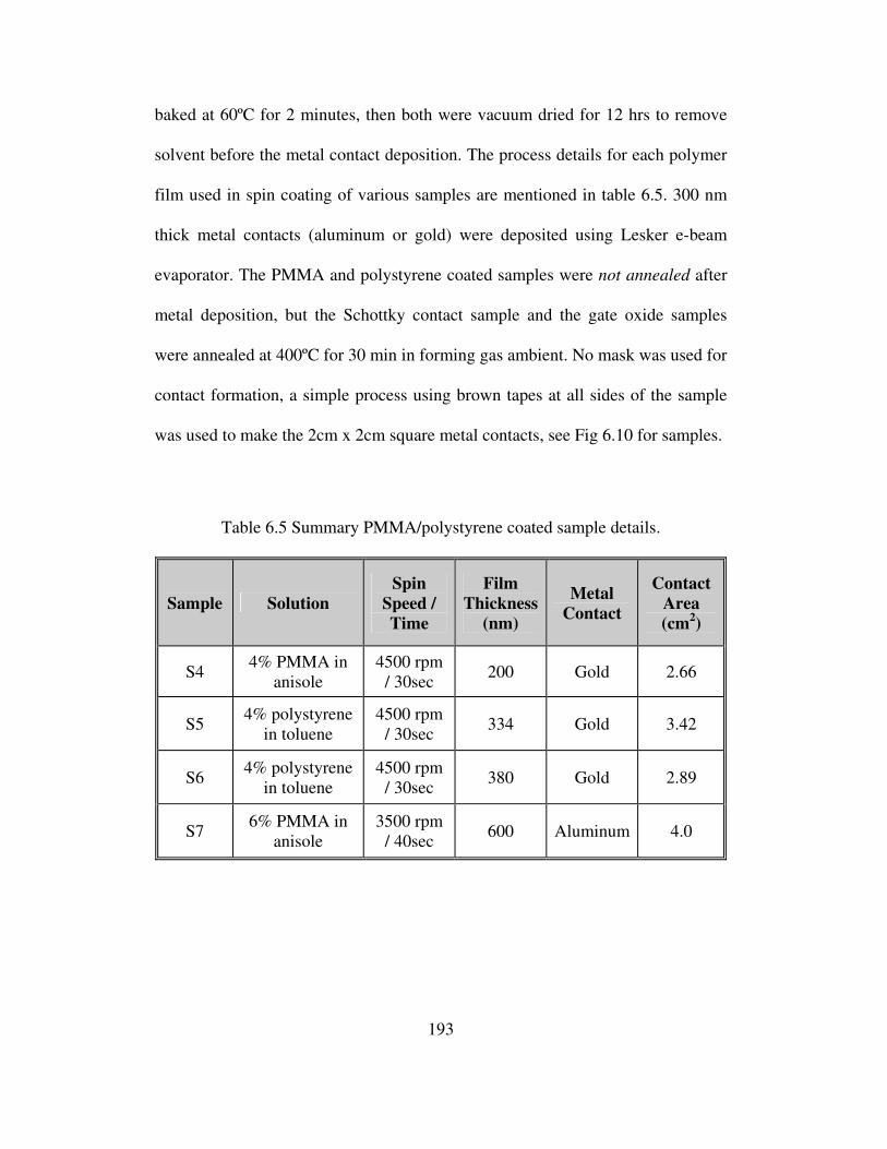
193
baked at 60ºC for 2 minutes, then both were vacuum dried for 12 hrs to remove
solvent before the metal contact deposition. The process details for each polymer
film used in spin coating of various samples are mentioned in table 6.5. 300 nm
thick metal contacts (aluminum or gold) were deposited using Lesker e-beam
evaporator. The PMMA and polystyrene coated samples were not annealed after
metal deposition, but the Schottky contact sample and the gate oxide samples
were annealed at 400ºC for 30 min in forming gas ambient. No mask was used for
contact formation, a simple process using brown tapes at all sides of the sample
was used to make the 2cm x 2cm square metal contacts, see Fig 6.10 for samples.
Table 6.5 Summary PMMA/polystyrene coated sample details.
Sample Solution
Spin
Speed /
Time
Film
Thickness
(nm)
Metal
Contact
Contact
Area
(cm2)
S4 4% PMMA in
anisole 4500 rpm
/ 30sec 200 Gold 2.66
S5 4% polystyrene
in toluene 4500 rpm
/ 30sec 334 Gold 3.42
S6 4% polystyrene
in toluene 4500 rpm
/ 30sec 380 Gold 2.89
S7 6% PMMA in
anisole 3500 rpm
/ 40sec 600 Aluminum 4.0

194
(a) (b)
Fig. 6.10. HRS substrates (a) gold contact, and (b) aluminum contact.
6.5.3. Impedance Spectroscopy – Bare HRS without Any Contacts
The first experiment was to try the easiest option that is to put the 2cm x 2cm
piece of HRS wafer between the two metal plates of the sample holder. This
forms two Schottky contacts on both sides of the wafer and can be represent by a
series arrangement of 3 parallel RC circuits Rdep1Cdep1-RsubCsub-Rdep2Cdep2 as
shown in Fig. 6.11(a) and the fitting mathematical model is given by the
impedance transfer function Z(s) in Eqn. 6.2, where Rdep1Cdep1 = parallel
combination of resistance and capacitance of the depletion layer due to the top
Schottky contact, RSubCSub = parallel combination of substrate resistance and
capacitance, and Rdep2Cdep2 = parallel combination of resistance and capacitance
of depletion layer due to the bottom Schottky contact. The mathematical model
was curve fitted to the experimental data using MEISP and MATLAB software
using CNLS algorithm, the fitted results are shown in Fig 6.11(b). After curve
fitting, the modeled parameters are Rdep1 = 8.75x10⁵ Ω, Cdep1 = 3.42x10⁻¹⁰ F, Rsub
= 2.44x10³ Ω, Csub = 2.46x10⁻¹⁰ F, Rdep2 = 4.88x10⁶ Ω, Cdep2 = 6.75x10⁻¹⁰ F.

195
Using Eqn. 6.1, for Rsub = 2.44 kΩ, thickness = 741 µm, and Area = 3.14cm2 ⇒
substrate resistivity ρsub = 103 kΩ.cm. This is a very high value compared to the
expected value of around 1 kΩ.cm. The mechanical contacts do not form a
uniform strong contact with the silicon and the contact resistance dominates,
which is believed to affect the overall measurement. Hence, only mechanical
contact on bare silicon is not suitable for resistivity extraction using Impedance
Spectroscopy.
( ) ( ) ( )sCR
R
sCR
R
sCR
RsZ
depdep
dep
subsub
sub
depdep
dep
22
2
11
1
111)(
++
++
+= (6.2)
0
50
100
150
200
-80
-60
-40
-20
0
10-1 101 103 105 107
Impedan
ce (
dB
)
Phase (
De
g)
Frequency (Hz)
Vac = 25mV
Fitted (RC-RC-RC)
Measured
ρρρρcalc = 100kΩΩΩΩ.cm
Mechanical Contact
(a) (b)
Fig. 6.11. Impedance Spectroscopy: bare Si with mechanical probe contacts only.
(a) Device structure and equivalent circuit, (b) curve fitting, measured and model.
6.5.4. Impedance Spectroscopy – HRS with Top Gate Oxide and Al Contact
The second experiment was based on a MOS capacitor structure with no
bottom contacts. The devices had 900 µm diameter aluminum gates on 112 nm

196
thick SiO2 grown on the polished side of the wafer. Silver paste was used to
contact the top gate and the back side to a sample holder having coaxial cable
connections as shown in Fig 6.12(c). The approximate contact area is 0.196 cm2
(≈ 5 mm diameter silver paste). It can be represented by a series arrangement of
Cox-RsubCsub-RdepCdep as shown in Fig. 6.12(a) and the fitting mathematical model
is given by the impedance transfer function Z(s) in Eqn. 6.3, where Cox = oxide
capacitance of the top gate oxide, RSubCSub = parallel combination of substrate
resistance and capacitance, and RdepCdep = parallel combination of resistance and
capacitance of depletion layer due to the bottom Schottky contact (silver paste on
silicon). The mathematical model was curve fitted to the experimental data using
MEISP and MATLAB software using CNLS algorithm, the fitted results are
shown in Fig 6.12(b). After curve fitting, the modeled parameters are Cox =
1.39x10⁻⁹ F, Rsub = 2.88x10³ Ω, Csub = 3.25x10⁻¹² F, Rdep = 6.57x10³ Ω, Cdep =
1.38x10⁻¹⁰ F. Using Eqn. 6.1, for Rsub = 2.88 kΩ, thickness = 760 µm, and Area =
0.196cm2 ⇒ substrate resistivity ρsub = 7.52 kΩ.cm. Though this resistivity is
high compared to the expected value of around 1 kΩ.cm, but it is not excessively
high like the mechanical contacts.
This experiment showed that avoiding direct contacts to the substrate or
making strong metal silicon contacts can yield better results. So it was decided to
use a dielectric layer that can be formed without any thermal step, has uniform
thickness without defects, and creates a strong bond with silicon. In subsequent
experiments, proper contact formation was the main focus.

197
( ) ( )sCR
R
sCR
R
sCsZ
depdep
dep
subsub
sub
ox ++
++=
111
)( (6.3)
0
50
100
150
200
-80
-60
-40
-20
0
10-1 101 103 105 107
Impedan
ce (
dB
)
Phase (
De
g)
Frequency (Hz)
Vac = 25mV
Fitted (C-RC-RC)
Measured
ρρρρcalc = 7.52kΩΩΩΩ .cm
Top Gate Oxide
(a) (b)
(c)
Fig. 6.12. Impedance Spectroscopy – Si sample with top gate oxide and Al
contact and bottom silver paste contact. (a) Device structure and equivalent
circuit, (b) curve fitting measured and model, (c) device in the sample holder.
6.5.5. Impedance Spectroscopy – Bare HRS with Teflon Sheets on Both Sides
The next experiment was to use a dielectric layer between the silicon and the
sample holder metal contacts, on both sides, to make a capacitive structure and
Devices Sample Holder
Co-axial Connectors
Silver paste connection

198
avoid the issues due to contact imperfections. So the easiest option was to use a
thin Teflon sheet (100 µm) as a dielectric on both sides of the silicon sample.
Figure 6.13 shows the device structure and the equivalent circuit in (a) and the
impedance vs. frequency in (b). But the results were inconclusive, it was mainly
dominated by the Teflon film as an insulator and no equivalent circuit could be
properly fitted to the measured data.
0
2
3
5
6
8
-80
-60
-40
-20
0
10-1 101 103 105 107
Impedan
ce (
Ohm
)
Phase (
De
g)
Frequency (Hz)
25mV
1V
tTeflon=100µµµµm
(a) (b)
Fig. 6.13. Impedance Spectroscopy – Si sample with Teflon film as top and
bottom gate dielectric and mechanical contacts. (a) Device structure and
equivalent circuit, (b) impedance vs. frequency plot - inconclusive.
6.5.6. Impedance Spectroscopy – HRS with Polystyrene and PMMA Thin
Films and Gold Contacts
In order to address the contact issue and avoid thermal oxide which may cause
resistivity changes due to thermal donor formation as we studied earlier; a new
approach using polymer film as dielectric was examined. Two types of devices

199
were fabricated, one with a thin film of PMMA or polystyrene on both top
(smooth) and bottom (rough) surfaces of HRS substrate and another with the
polymer film only on the top surface of the HRS substrate, as shown in the device
schematic in Fig. 6.14. There were 3 samples used in this experiment: (a) 334 nm
spin coated polystyrene film on both sides using 4% polystyrene solution in
toluene, (b) 380 nm spin coated polystyrene film on smooth surface only using
4% polystyrene solution in toluene, and (c) 200 nm spin coated PMMA film on
both sides using 6% PMMA in anisole. All samples had evaporated gold contacts
on both sides. All film thicknesses were measured by ellipsometry.
Fig. 6.14 Device schematics with top and bottom polymer dielectrics and the
corresponding fitted equivalent circuit.
Then the equivalent circuit and the mathematical model were derived using IS
approach as shown in Fig. 6.14 and Eqn. 6.4, respectively. It was found that all
three devices used in this experiment can be modeled as a series combination of
Rcontact-CTopGate-RsubCsub-Rfilm/depCfilm/dep. Rcontact = contact resistance, CTopGate = top
gate capacitance, RsubCsub = parallel combination of substrate resistance and

200
capacitance, and RfilmCfilm = parallel combination of leakage resistance and
capacitance of bottom dielectric, if present, and RdepCdep = parallel combination
of resistance and capacitance of depletion layer due to the bottom Schottky
contact (Gold). The mathematical model was curve fitted to the experimental data
using MEISP and MATLAB software using CNLS algorithm, the fitted plots are
shown in Fig 6.15(a, b, c). When the thin film (dielectric) is present on both sides
of the HRS substrate, the extracted resistivity is 1.13 kΩ.cm for PMMA and 1.24
kΩ.cm for polystyrene, which is very close to the desired resistivity ≈ 1 kΩ.cm.
But when the film is on the top surface only, the extracted resistivity is 2.03
kΩ.cm. It is believed, without the bottom dielectric the depletion layer due to the
Schottky contact is in series with the substrate affects the results. The results are
summarized along with the device cross sections in Fig. 6.15(d).
( ) ( )sCR
R
sCR
R
sCRsZ
depfilmdepfilm
depfilm
subsub
sub
TopGate
Contact
//
/
111
)(+
++
++= (6.4)

201
0
10
20
30
40
50
60
70
80
-80
-60
-40
-20
0
100 101 102 103 104 105 106 107
Imp
edan
ce (
dB
)
Pha
se (
De
g)
Frequency (Hz)
Polystyrene Both Sides
Fitted (R-C-RC-RC)
Measured
ρρρρcalc = 1.24kΩΩΩΩ.cm Vac = 10mV
tfilm = 334nm
0
10
20
30
40
50
60
70
80
-80
-60
-40
-20
0
101 102 103 104 105 106 107
Impe
dan
ce
(dB
)
Pha
se (
De
g)
Frequency (Hz)
Vac = 10mV
Fitted (R-C-RC-RC)
Measured
PMMA Both Sides
ρρρρcalc = 1.13kΩΩΩΩ.cm
tfilm = 200nm
(a) (b)
0
10
20
30
40
50
60
70
80
-80
-60
-40
-20
0
10-1 100 101 102 103 104 105 106 107
Imp
eda
nce
(dB
)
Pha
se
(D
eg)
Frequency (Hz)
Polystyrene on Top only
Fitted (R-C-RC-RC)
Measured
ρρρρcalc = 2.03kΩΩΩΩ.cm Vac = 10mV
tfilm = 380nm
(c) (d)
Fig. 6.15. (a, b, c) Resistivity extraction from IS using curve fitting for various
dielectrics. (d) Device cross section with extracted Si resistivity.
6.5.7. Impedance Spectroscopy – HRS with PMMA Thick Films and Al
Contacts on Both Sides
The next approach was to use a thicker polymer film and aluminum contact for
resistivity extraction to see the effect of film thickness and different contact
material types. A thicker PMMA film (600nm) using 6% PMMA in anisole was

202
spin coated on both top (smooth) and bottom (rough) surfaces of HRS substrate
as shown in the device schematic in Fig. 6.16(a). The equivalent circuit and the
mathematical model were derived using IS approach as shown in Fig. 6.16(a) and
Eqn. 6.5, respectively. The device can be modeled as a series combination of
RtopCtop-Rsub-RbotCbot. RtopCtop = parallel combination of leakage resistance and
capacitance of top PMMA film, Rsub = substrate resistance, and RbotCbot = parallel
combination of leakage resistance and capacitance of bottom PMMA film. The
substrate could have been modeled by a parallel RC circuit like previous cases
but a resistive (Rsub) circuit gives a better matching between the experiment and
the model. The mathematical model was curve fitted to the experimental data
using MEISP and MATLAB software using CNLS algorithm, the fitted plots are
shown in Fig 6.16(b). With a thicker film (dielectric) on both sides of the HRS
substrate, the extracted substrate resistivity is 1.45 kΩ.cm, close to the previous
values and the expected resistivity ≈ 1 kΩ.cm.
( ) ( )sCR
RR
sCR
RsZ
botbot
bot
sub
toptop
top
+++
+=
11)( (6.5)

203
0
20
40
60
80
100
120
-80
-60
-40
-20
0
100 101 102 103 104 105 106 107
Impe
da
nce
(dB
)
Phase
(D
eg
)
Frequency (Hz)
Vac = 5mV
PMMA Both Sides
Fitted (RC-R-RC)
Measured
ρρρρcalc = 1.45kΩΩΩΩ.cm
tfilm = 600nm
(a) (b)
Fig. 6.16. Impedance Spectroscopy – HRS sample with thick PMMA film
(600nm) on both sides and aluminum contacts. (a) Device structure and
equivalent circuit, (b) curve fitting - measured and model.
6.5.8. Impedance Spectroscopy – HRS Sample with Only Al Contacts on
Both Sides (Schottky Contacts)
It was discussed previously that the contact imperfection plays a major role in
measurement difficulties, so to address that issue it was decided to make metal
contacts by evaporating 300 nm aluminum on both surfaces of the HRS substrate
as shown in the device schematic in Fig. 6.17(a). The contacts were annealed at
450ºC in forming gas ambient for 30 minutes. The equivalent circuit and the
mathematical model were derived using IS approach as shown in Fig. 6.17(a) and
Eqn. 6.6, respectively. The device can be modeled as a series combination of
RtopCtop-Rsub-RbotCbot. RtopCtop and RbotCbot = parallel combination of leakage
resistance and capacitance of the top and bottom Schottky depletion layers
respectively, Rsub = substrate resistance. The mathematical model was curve fitted

204
to the experimental data using MEISP and MATLAB software using CNLS
algorithm, the fitted plots are shown in Fig 6.17(b). The substrate could have
been modeled by a parallel RC circuit like previous cases but only resistive (Rsub)
circuit gives a better matching between the experiment and the model. With
aluminum contacts on both sides of the HRS substrate, the extracted substrate
resistivity ρsub = 2.24 kΩ.cm higher than expected but similar to the results
obtained by one side coated polystyrene structure in section 6.5.6. The high
resistive depletion layers on both sides might be causing an increase in the
measured substrate resistivity. So the suggestion is to avoid direct contact to the
silicon surface and use a dielectric layer.
( ) ( )sCR
RR
sCR
RsZ
botbot
bot
sub
toptop
top
+++
+=
11)( (6.6)
0
20
40
60
80
100
120
-80
-60
-40
-20
0
100 101 102 103 104 105 106 107
Imp
edan
ce (
dB
)
Phase (
De
g)
Frequency (Hz)
Vac = 10mV
AL Both Sides
Fitted (RC-R-RC)
Measured
ρρρρcalc = 2.24kΩΩΩΩ.cm
(a) (b)
Fig. 6.17. Impedance Spectroscopy – HRS sample with only aluminum contacts
on both sides. (a) Device structure and equivalent circuit, (b) curve fitting -
measured and model.

205
6.5.9. Impedance Spectroscopy – HRS with Thermal Oxide and Al Contacts
on Both Sides
It was also decided to try a device with gate oxide on both sides of the HRS
substrate for Impedance Spectroscopy as it is the best dielectric on silicon even
though it involves high temperature steps which may affect HRS substrate due to
thermal donors. Thermal oxide (47 nm) was grown on both sides of the HRS
substrate and 300 nm aluminum contacts were evaporated on both sides as shown
in the device schematic in Fig. 6.18 (a). The equivalent circuit and the
mathematical model were derived using IS approach as shown in Fig. 6.18 (a)
and Eqn. 6.7, respectively. The device can be modeled as a series combination of
RC-Rsub. RC = parallel combination of leakage resistance and capacitance of top
oxide layer, Rsub = substrate resistance. This particular model is different from
previous models but it best fits the measurement for this structure in this
experiment compared to an RC-R-RC or RC-RC-RC structures as used in
previous models. The mathematical model was curve fitted to the experimental
data using MEISP and MATLAB software using CNLS algorithm, the fitted plots
are shown in Fig 6.18(b). With a gate oxide (dielectric) on both sides of the HRS
substrate, the extracted substrate resistivity ρsub = 1.46 kΩ.cm, close to the
expected value ≈ 1kΩ.cm.
subRRCs
RsZ +
+=
1)( (6.7)

206
0
20
40
60
80
100
120
-80
-60
-40
-20
0
100 101 102 103 104 105 106 107
Impedan
ce (
dB
)
Phase (
De
g)
Frequency (Hz)
Vac = 5mV
OXIDE Both Sides
Fitted (RC-R)
Measured
ρρρρcalc = 1.46kΩΩΩΩ.cm
tox = 47nm
(a) (b)
Fig. 6.18. Impedance Spectroscopy – HRS sample with thermal oxide (47nm) on
both sides and aluminum contacts. (a) Device structure and equivalent circuit, (b)
curve fitting - measured and model.
6.5.10. Impedance Spectroscopy - Summary of All Experiments
Impedance Spectroscopy analysis for all different device types are
summarized in Fig 6.19 and Table 6.6. It shows, using a dielectric layer on both
sides yields a more accurate result close to the expected value ≈ 1kΩ.cm.
Comparison of All Impedance Spectroscopy Measurements
7.52
1.13 1.24
2.031.45
2.24
1.46
0
1
2
3
4
5
6
7
8
9
10
Bare Silicon &
Mechanical
contact
Top Gate
Oxide & Silver
paste contact
PMMA thin
film both sides
& Gold
contact
Polystyrene
thin film both
sides & Gold
contact
Polystyrene
thin film one
side & Gold
contact
PMMA thick
film both sides
& AL contact
Bare Si and
AL contact
both sides
Gate Ox both
sides & AL
contact
Re
sis
tiv
ity
(k
Oh
m.c
m)
Expected Resistivity ≈ 1kΩΩΩΩ .cm
100
Fig. 6.19. Summary of all Impedance Spectroscopy measurements.

207
Table 6.6 Summary of all Impedance Spectroscopy measurements.
Device Type Fitted Equivalent Circuit Mathemati
cal Model
Resistivity
(kΩΩΩΩ.cm)
Bare silicon and mechanical contacts both sides
RC-RC-RC 100
Oxide on top and silver paste contacts both sides
C-RC-RC 7
Teflon film and mechanical contacts both sides
Did not work
Not Available
PMMA film (200 nm) both sides and gold contacts
1.13
Polystyrene film (334 nm) both sides and gold contacts
1.24
Polystyrene film (380 nm) on top and gold contacts both sides
R-C-RC-RC
2.03
PMMA film (600 nm) both sides and aluminum contacts
RC-R-RC 1.45
Bare silicon and aluminum contacts both sides
RC-R-RC 2.24
Oxide both sides (47nm) and aluminum contacts
RC-R 1.46

208
6.6. Conclusion
In this chapter, various commonly used resistivity measurement techniques
such as four-point probe, Hall measurement method, C-V characterization
technique were used to measure the resistivity of high-resistive silicon and it was
shown that it is very difficult to measure the resistivity of HRS wafers using these
techniques. The measured resistivity differed for each technique. The Schottky
nature of the contact was found to pose a major challenge in these measurements.
A novel resistivity measurement technique based on Impedance Spectroscopy
was proposed, which provided a more accurate result close to the expected value.
Various device structures were used during IS and it was found that measurement
using a mechanical contact to the substrate is not suitable. Evaporated aluminum
contacts on both sides work better but the measurement is not completely
accurate due to the Schottky nature of the contacts. Using a dielectric such as a
thermal oxide or a polymer on both sides of the HRS substrate provides a more
accurate result close to the expected value. It was shown that HRS substrate with
spin-coated polymer film such as polystyrene and PMMA along with aluminum
or gold contacts on both sides can be used as an effective test structure to extract
resistivity using IS. Using the dielectric layer only on one side of the substrate
does not yield accurate result. The polymer films avoid any thermal steps thereby
reducing the possibility of thermal donor creation in HRS wafers which are
known to change the polarity and resistivity of low doped p-type substrates. This
novel technique is simple, uses regular capacitive structure and entails very
simple and minimal processing. The samples and the contacts can be larger,

209
covering most of the sample area, unlike the Hall measurement method. So this
Impedance Spectroscopy based approach using polymer films can be used for
resistivity measurement as it takes into account the contact effects and other
device related anomalies and avoids thermal donor creations steps.

210
CHAPTER 7. CONCLUSION AND FUTURE WORK
7.1. Conclusion
High-resistivity silicon wafers are gaining importance in the modern era of
mobile technology and high-performance system-on-chip circuits due to their
ability to lower the coupling between devices and provide low-loss substrates for
high speed and system integration. This research is focused on the
characterization of high-resistivity bulk and SOI wafers to understand the C-V
behavior of these wafers, understand the coupling reduction abilities, and to
explore various ways to measure the resistivity of these wafers.
The C-V characteristics of HRSOI were studied in detail by experiments and
simulation with a metal contact directly on the film. Various factors affecting the
C-V characteristics were studied: frequency, size of the top film contact, effect of
the contact size and the substrate size, film thickness, film and substrate doping
concentrations, carrier lifetimes, contact work-function, and type of film contact
i.e., Schottky or Ohmic, radiation, light, temperature and annealing. The doping
type of HRSOI substrate can undergo a reversal from p- to n-type at low substrate
doping concentration due to the formation of oxygen thermal donors after
annealing. The C-V plots showed spreading of capacitance following an “S”
shape at a particular bias mostly where the capacitance changes from a value
proportional to the contact area to a value 5 to 10 times larger. The spreading is
mainly due to the floating body and the contact being directly on the film, and the
RC transmission line behavior of the film/BOX/substrate interface. The
capacitance spreading is not observed when there is a gate oxide on the silicon

211
film. This shape of the C-V plot is mainly due to the Schottky contact and its
work-function. The RC transmission line behavior of the film and the substrate
plays a significant role in the bias spreading and the shape of the C-V
characteristic. At higher frequencies the ac signal flows very close to the contact
due to the low-pass filter nature of the RC circuit and spreads less into the other
part of the film giving smaller capacitances than at a lower frequency.
Substrate coupling in high-resistivity SOI substrates was studied and the
effects of various factors such as: substrate resistivity, separation between
devices, buried oxide (BOX) thickness, radiation, temperature, annealing, and
light on crosstalk was studied using both experiments and simulations. Both
experiments and simulations showed that cross talk reduces as substrate
resistivity increases. HRSOI has better substrate coupling prevention capability
than LRSOI substrates but in HRSOI wafers crosstalk did not reduce significantly
beyond a certain resistivity.
A new approach to reduce crosstalk has been proposed, which uses air gaps at
the BOX/substrate interface to reduce crosstalk. Larger air gaps are more
effective in reducing crosstalk than smaller ones located only below the noisy and
the sensitive devices. Impact of air gap in reducing crosstalk is more prominent in
LRSOI than HRSOI. Another approach is to use a porous layer at the BOX-
substrate interface which can lower the coupling.
Owing to their very low doping concentrations and the presence of oxygen in
CZ wafers, HRS wafers pose a challenge in resistivity measurement using the
conventional techniques such as: four-point probe and Hall measurement. It was

212
shown with measurement that it is difficult to measure the resistivity of HRS
wafers accurately and repeatedly using the commonly used resistivity
measurement methods such as four-point probe, Hall measurement, capacitance-
voltage methods. A novel resistivity measurement technique based on Impedance
Spectroscopy was proposed and implemented, which provides a more accurate
result close to the expected value. Various device structures were used during IS
and it was found that measurement using a mechanical contact to the substrate is
not suitable. Evaporated aluminum contacts on both sides work better but the
measurement is not completely accurate due to the Schottky nature of the
contacts. Using a dielectric such as a thermal oxide or a polymer on both sides of
the HRS substrate provided a more accurate result close to the expected value. It
was shown that HRS substrate with spin-coated polymer film such as polystyrene
and PMMA along with aluminum or gold contacts on both sides can be used as
effective test structure to extract resistivity using IS. Using the film on only one
side of the substrate does not yield accurate results. These polymer films avoid
any thermal steps thereby reducing the possibility of thermal donor creation in
HRS wafer which are known to change the polarity and resistivity of low-doped
p-type substrates. This novel technique is simple, uses regular capacitive structure
and entails very simple minimal processing. So this Impedance Spectroscopy
based approach using polymer films can be used for resistivity measurement as it
takes into account the contact effects and other device related effects.

213
7.2. Future Work
The suggested crosstalk minimization technique using airgap below the BOX
can be experimentally implemented. The proposed Impedance spectroscopy
approach using polymer dielectrics can be further verified and refined to make it
an industry applicable product using HRS samples with various substrate
resistivities.

214
REFERENCES
[1] T. M. Hyltin, "Microstrip transmission on semiconductor dielectrics," IEEE Trans. Microwave Theory Tech., vol. MTT-13, pp. 777-781, November, 1965.
[2] B. W. Battershall and S. P. Emmons, "Optimization of diode structures for monolithic integrated microwave circuits," IEEE J Solid State Circuits,
vol. SC-3, pp. 107-112, June, 1968.
[3] A. Rosen, M. Caulton, P. Stabile, A. M. Gombar, W. M. Janton, P. W. Chung, J. F. Corboy and C. W. Magee, "Silicon as a millimeter-wave monolithically integrated substrate-a new look," RCA Review, vol. 42, pp. 633-660, December, 1981.
[4] K. M. Strohm, J. Buechler, P. Russer and E. Kasper, "Silicon high resistivity substrate millimeter-wave technology," in Microwave and
Millimeter-Wave Monolithic Circuits, pp. 93-97, 1986.
[5] M. H. Hanes, A. K. Agarwal, T. W. O'Keeffe, H. M. Hobgood, J. R. Szedon, T. J. Smith, R. R. Siergiej, P. G. McMullin, H. C. Nathanson, M. C. Driver and R. N. Thomas, "MICROX-an all-silicon technology for monolithic microwave integrated circuits," Electron Device Letters, IEEE,
vol. 14, pp. 219-221, 1993.
[6] A. C. Reyes, S. M. El-Ghazaly, S. Dorn, M. Dydyk, D. K. Schroder and H. Patterson, "High resistivity si as a microwave substrate," in Electronic
Components and Technology Conference, 1996. Proceedings., 46th, pp. 382-391, 1996,.
[7] K. Benaissa, Jau-Yuann Yang, D. Crenshaw, B. Williams, S. Sridhar, J. Ai, G. Boselli, S. Zhao, S. Tang, S. Ashburn, P. Madhani, T. Blythe, N. Mahalingam and H. S. Shichijo, "RF CMOS on high-resistivity substrates for system-on-chip applications," IEEE Trans. Electron Devices, vol. 50, pp. 567-576, March, 2003.
[8] C. S. Fuller, J. A. Ditzenberger, N. B. Hannay and E. Buehler, "Resistivity changes in silicon single crystals induced by heat treatment," Acta
Metallurgica, vol. 3, pp. 97-99, January, 1955.
[9] W. Kaiser, H. L. Frisch and H. Reiss, "Mechanism of the formation of donor states in heat-treated silicon," Physical Review, vol. 112, pp. 1546-1554, December, 1958.

215
[10] A. Kanamori and M. Kanamori, "Comparison of two kinds of oxygen donors in silicon by resistivity measurements," J. Appl. Phys., vol. 50, pp. 8095-101, December, 1979.
[11] D. K. Schroder, Semiconductor Material and Device Characterization.
NY: Wiley Interscience, 2006.
[12] L. J. McDaid, S. Hall and W. Eccleston, "Interpretation of capacitance-voltage characteristics on silicon-on-insulator (SOI) capacitors," Solid-
State Electronics, vol. 32, pp. 65-68, 1989.
[13] D. Flandre and d. W. Van, "A new analytical model for the two-terminal MOS capacitor on SOI substrate," IEEE Electron Device Lett., vol. 9, pp. 296-9, June, 1988.
[14] F. A. Ikraiam, R. B. Beck and A. Jakubowski, "Modeling of SOI-MOS capacitors C-V behavior: partially- and fully-depleted cases," IEEE Trans.
Electron Devices, vol. 45, pp. 1026-1032, May, 1998.
[15] D. Flandre, T. Loo, P. Verlinden and V. D. Wiele, "Interpretation of quasi-static C-V characteristics of MOSOS capacitors on SOI substrates," Electron. Lett., vol. 27, pp. 43-44, 1991.
[16] J. Colinge, Silicon-On-Insulator Technology:Materials to VLSI. Boston: Kluwer, 1991.
[17] L. D. Smith, H. R. Farmer, M. Kunesh, M. A. Massetti, D. Willmott, R. Hedman, R. Richetta and T. J. Schmerbeck, "A CMOS-based analog standard cell product family," Solid-State Circuits, IEEE Journal of, vol. 24, pp. 370-379, 1989.
[18] T. J. Schmerbeck, R. A. Richetta and L. D. Smith, "A 27MHz mixed Analog/digital magnetic recording channel DSP using partial response signalling with maximum likelihood detection," in Solid-State Circuits
Conference, 1991. Digest of Technical Papers. 38th ISSCC., 1991 IEEE
International, pp. 136-304, 1991.
[19] D. K. Su, M. J. Loinaz, S. Masui and B. A. Wooley, "Experimental results and modeling techniques for substrate noise in mixed-signal integrated circuits," IEEE J Solid State Circuits, vol. 28, pp. 420-430, April, 1993.
[20] M. Rahim, Bor-Yuan Hwang and J. Foerstner, "Comparison of SOI versus bulk silicon substrate crosstalk properties for mixed-mode IC's," in SOI
Conference, 1992. IEEE International, pp. 170-171, 1992.

216
[21] K. Joardar, J. Ford and P. Welch, "A simple approach to modeling cross-talk in integrated circuits," in Bipolar/BiCOMS Circuits and Technology
Meeting, 1993., Proceedings of the 1993, pp. 114-117i1993.
[22] A. L. Caviglia, R. C. Potter and L. J. West, "Microwave performance of SOI n-MOSFET's and coplanar waveguides," Electron Device Letters, vol. 12, pp. 26-27, 1991.
[23] J. Raskin, A. Viviani, D. Flandre and J. Colinge, "Substrate crosstalk reduction using SOI technology," IEEE Trans. Electron Devices, vol. 44, pp. 2252-2261, 1997.
[24] W. H. Mitchell, "Cryostat for measuring the electrical properties of high resistance semiconductors at low temperatures," J. Sci. Instrum., vol. 36, pp. 134; 308-136, 1959.
[25] R. J. Mattauch, "The Measurement of a High Impedance Source Having Shunt Capacitance," Rev. Sci. Instrum., vol. 41, pp. 592-593, April, 1970.
[26] G. Fischer, D. Greig and E. Mooser, "Apparatus for the Measurement of Galvanomagnetic Effects in High Resistance Semiconductors," Rev. Sci.
Instrum., vol. 32, pp. 842-846, July, 1961.
[27] J. H. Fermor and A. Kjekshus, "Servo-Controlled Measuring Bridge for Semiconductors of High Resistivity," Rev. Sci. Instrum., vol. 36, pp. 763-766, June, 1965.
[28] G. H. Heilmeier and S. E. Harrison, "Charge Transport in Copper Phthalocyanine Single Crystals," Phys. Rev., vol. 132, pp. 2010, December, 1963.
[29] I. Eisele and L. Kevan, "Double Modulation Method for Hall Effect Measurements on Photoconducting Materials," Rev. Sci. Instrum., vol. 43, pp. 189-194, February, 1972.
[30] E. E. Olson and J. E. Wertz, "A High Impedance ac Hall Effect Apparatus," Rev. Sci. Instrum., vol. 41, pp. 419-421, March, 1970.
[31] D. Colman, "High Resistivity Hall Effect Measurements," Rev. Sci.
Instrum., vol. 39, pp. 1946-1948, December, 1968.
[32] MEMC. High resistivity wafers. MEMC. Available: http://www.memc.com/assets/file/products/advanced-materials/hi-low%20res_rev10102003.pdf, 2011.
[33] ITRS. "International technology roadmap for semiconductors 2009 edition - executive summary". ITRS, USA. Available:

217
http://www.itrs.net/Links/2009ITRS/2009Chapters_2009Tables/2009_ExecSum.pdf, 2009.
[34] S. Laurent and E. Desbonnets. "RF substrate technologies for mobile communications", SOITEC, Available: http://www.soitec.com/pdf/RF_SubstratesTechnologies_2011-07-07.pdf, 2011.
[35] . Yuen, K. Laursen, D. Chu, Yi-Ching Pao, A. Chernyakov and P. Heide, "A compact flip chip single die WiFi FEM for smart phone application," in 2010 IEEE/MTT-S International Microwave Symposium - MTT 2010, pp. 1098-101, 2010.
[36] T. Henderson, J. Middleton, J. Mahoney, S. Varma, T. Rivers, C. Jordan and B. Avrit, "High-Performance BiHEMT HBT / E-D pHEMT Integration," GaAs MANTECH Digest, pp. 247-250, 2007.
[37] G. Imthurn, "The history of Silicon-on-Sapphire," Peregrine
Semiconductor, vol. 1, 2007.
[38] D. Nobbe, "RF front end integration in UltraCMOS," IMS Workshop WSA,
2009.
[39] A. Botula, A. Joseph, J. Slinkman, R. Wolf, Z. -. He, D. Ioannou, L. Wagner, M. Gordon, M. Aboukhalil, R. Phelps, M. Gautsch, W. Abadeer, D. Harmon, M. Levy, J. Benoit and J. Dunn, "A thin-film SOI 180nm CMOS RF switch technology," in 2009 9th Topical Meeting on Silicon
Monolithic Integrated Circuits in RF System, SiRF'09, January 19, 2009 -
January 21, pp. 152-155, 2009.
[40] D. C. Kerr, J. M. Gering, T. G. McKay, M. S. Carroll, C. R. Neve and J. Raskin, "Identification of RF harmonic distortion on si substrates and its reduction using a trap-rich layer," in 2008 IEEE Topical Meeting on
Silicon Monolithic Integrated Circuits in RF Systems, SiRF, January 23,
2008 - January 25, pp. 151-154, 2008.
[41] R. A. Bianchi, F. Monsieur, F. Blanchet, C. Raynaud and O. Noblanc, "High voltage devices integration into advanced CMOS technologies," in 2008 IEEE International Electron Devices Meeting, IEDM 2008,
December 15, 2008 - December 17, 2008.
[42] A. Joseph, P. Gammel, P. Rabbeni, R. Wolf and J. Dunn, "Silicon solutions for RF front-end applications," in 2011 IEEE 11th Topical
Meeting on Silicon Monolithic Integrated Circuits in RF Systems, SiRF
2011, January 16, 2011 - January 19, 2011, pp. 109-112, 2011.

218
[43] F. Gianesello, C. Durand, R. Pilard, D. Petit, J. Penard, S. Jan, D. Gloria, B. Rauber and C. Raynaud, "Integration of cellular front end modules on advanced high resistivity SOI RF CMOS technology," in 2011 IEEE
Topical Conference on Power Amplifiers for Wireless and Radio
Applications, PAWR 2011, January 16, 2011 - January 19, 2011, pp. 29-32, 2011.
[44] D. V. Van, M. Agostinelli, S. -. Choi, G. Curello, H. Deshpande, M. El-Tanani, W. Hafez, U. Jalan, L. Janbay, M. Kang, K. -. Koh, K. Komeyli, H. Lakdawala, J. Lin, N. Lindert, S. Mudanai, J. Park, K. Phoa, A. Rahman, J. Rizk, L. Rockford, G. Sacks, K. Soumyanath, H. Tashiro, S. Taylor, C. Tsai, H. Xu, J. Xu, L. Yang, I. Young, J. -. Yeh, J. Yip, P. Bai and C. -. Jan, "A 32nm low power RF CMOS SOC technology featuring high-k/metal gate," in 2010 Symposium on VLSI Technology, VLSIT 2010,
June 15, 2010 - June 17, 2010, pp. 137-138, 2010.
[45] J. Czochralski, "Ein neues Verfahren zur Messung der Kristallisationsgeschwindigheit der Metalle," Z. Phys. Chemie, vol. 92, pp. 219-221, 1918.
[46] G. Teal and J. B. Little, "Growth of Germanium Single Crystals," Phys.
Rev., vol. 78, pp. 647, 1950.
[47] F. Shimura, Ed., Oxygen in Silicon. San Diego, CA: Academic Press Inc., 1994.
[48] T. Abe, VLSI Electronics Microstructure Science. New York: Academic Press, 1985.
[49] W. C. Dash, "Silicon crystals free of dislocations," J. Appl. Phys., vol. 29, pp. 736-737, April, 1958.
[50] Wikipedia, "Czochralski Process," Wikipedia, vol. 2011, September, 2011.
[51] Olli Anttila. "Manufacture of high resistivity, low oxygen Czochralski silicon," Available: http://en.wikipedia.org/wiki/Zone_melting, pp. 39. 2005.
[52] W. G. Pfann, Zone Melting. New York: John Wiley & Sons, 1966.
[53] K. E. Benson, W. Lin and E. P. Martin, "Fundamental aspects of Czochralski silicon crystal growth for VLSI," in Semiconductor Silicon
1981, pp. 33-48, 1981.
[54] W. Lin and D. W. Hill, "Large-diameter Czochralski silicon crystal growth," in Silicon Processing, pp. 24-38, 1983.

219
[55] G. Fiegl, "Recent advances and future directions in CZ-silicon crystal growth technology," Solid State Technol., vol. 26, pp. 121-131, 1983.
[56] H. P. Utech and M. C. Flemings, "Elimination of solute banding in indium antimonide crystals by growth in magnetic field," J. Appl. Phys., vol. 37, pp. 2021-2024, 1966.
[57] S. Chandrasekhar, "On the inhibition of convection by a magnetic field," Philosophical Magazine, vol. 43, pp. 501-532, May, 1952.
[58] M. Ohwa, T. Higuchi, E. Toji and M. Watanabe, "Growth of large diameter silicon single crystal under horizontal or vertical magnetic field," in Proceedings of the Fifth International Symposium on Silicon Materials
Science and Technology: Semiconductor Silicon 1986, pp. 117-28, 1986.
[59] T. T. Braggins and R. N. Thomas, "Oxygen in axial field magnetic Czochralski silicon," Electrochem. Soc. Ext. Abstr., vol. 169, pp. 351-354, 1986.
[60] K. Hoshi, N. Isawa, T. Suzuki and Y. Ohkubo, "Czochralski silicon crystals grown in a transverse magnetic field," J. Electrochem. Soc., vol. 132, pp. 693-700, 1985.
[61] K. Hoshi, T. Suzuki, Y. Okubo and N. Isawa, "Czochralski silicon crystal grown in transverse magnetic fields," Extended Abstracts Electrochem.
Soc., vol. 157, pp. 811, 1980.
[62] T. Suzuki, N. Isawa, Y. Okubo and K. Hoshi, "CZ Silicon Crystals Grown In A Transverse Magnetic Field," Proceedings - the Electrochemical
Society, vol. 81, pp. 90-100, 1981.
[63] W. Zulehner, "Historical overview of silicon crystal pulling development," Materials Science and Engineering B: Solid-State Materials for Advanced
Technology, vol. 73, pp. 7-15, 2000.
[64] W. G. Pfann, "Principles of zone-melting," American Institute of Mining
and Metallurgical Engineers -- Journal of Metals, vol. 4, pp. 747-753, 1952.
[65] P. H. Keck and M. J. E. Golay, "Crystallization of silicon from floating liquid zone," Physical Review, vol. 89, pp. 1297, 1953.
[66] H. C. Theuerer. 23 October 1962). US Patent No. 3,060,123 , 17 December 1952.
[67] Siltronic, "200 mm Float-zone," vol. 2011, 2011.

220
[68] Wikipedia. "Zone melting," Available: http://en.wikipedia.org/wiki/Zone_melting, 2011.
[69] H. Föll. "Float zone crystal growth," Available: http://www.tf.uni-kiel.de/matwis/amat/elmat_en/kap_6/advanced/t6_1_3.html, 2011.
[70] J. Meese, Ed., Neutron Transmutation Doping in Semiconductors. New York: Plenum Press, 1979.
[71] M. Tanenbaum and A. D. Mills, "Preparation of uniform resistivity n-type silicon by nuclear transmutation," Electrochemical Society -- Journal, vol. 108, pp. 171-176, 1961.
[72] TOPSIL Semiconductor Materials A/S. "FZ-NTD silicon for high power electronics," Available: www.topsil.com/files/pdf/NTD-ApplicationNote~.pdf, pp. 12, October, 2011.
[73] S. W. Jones. "Properties of silcion," IC Knowledge LLC. Available: http://www.icknowledge.com/misc_technology/SiliconChapter.pdf, 2008.
[74] J. R. Patel and A. R. Chaudhuri, "Oxygen precipitation effects on the deformation of dislocation-free silicon," J. Appl. Phys., vol. 33, pp. 2223-2224, July, 1962.
[75] I. Yonenaga, K. Sumino and K. Hoshi, "Mechanical strength of silicon crystals as a function of the oxygen concentration," J. Appl. Phys., vol. 56, pp. 2346-2350, October, 1984.
[76] S. Takasu, H. Otsuka, N. Yoshihiro and T. Oku, "WAFER BOW AND WARPAGE," Proceedings of the Conference on Solid State Devices, pp. 25-30, 1981.
[77] B. Leroy and C. Plougonven, "WARPAGE OF SILICON WAFERS," J.
Electrochem. Soc., vol. 127, pp. 961-970, 1980.
[78] K. Sumino, I. Yonenaga and A. Yusa, "Mechanical strength of oxygen-doped float-zone silicon crystals," Japanese Journal of Applied Physics,
vol. 19, pp. 763-766, December, 1980.
[79] T. Abe, K. Kikuchi, S. Shirai and S. Murakoa, "Impurities in silicon single crystals - a current view." in Semiconductor Silicon 1981, pp. 54-71, 1981.
[80] Siliconsultant, P.O. Box 1453, Evergreen, CO 80437 USA, "Silicon info: Single-crystal ingot growth," Available: http://www.siliconsultant.com/SIcrysgr.htm, 2010.

221
[81] S. Cristoloveanu and S. Li, Electrical Characterization of Silicon on
Insulator Materials and Devices. Boston: Kluwer, 1995.
[82] G. K. Celler and S. Cristoloveanu, "Frontiers of silicon-on-insulator," J.
Appl. Phys., vol. 93, pp. 4955-78, May, 2003.
[83] K. E. Bean and W. R. Runyan, "Dielectric isolation: Comprehensive, current and future," J. Electrochem. Soc., vol. 124, pp. 5C-12, January, 1977.
[84] A. Gupta and P. K. Vasudev, "Recent advances in hetero-epitaxial silicon-on-insulator technology. I," Solid State Technol., vol. 26, pp. 104-9, February, 1983.
[85] D. Pribat, L. M. Mercandalli, J. Siejka and J. Perriere, "Interface oxidation of epitaxial silicon deposits on (100) yttria stabilized cubic zirconia," J.
Appl. Phys., vol. 58, pp. 313-20, July, 1985.
[86] H. J. Leamy, "Laser fabrication of silicon on dielectric substrates," in Proceedings of the Materials Research Society Annual Meeting, pp. 459-504, 1982.
[87] G. K. Celler, "Laser crystallization of thin Si films on amorphous insulating substrates," J. Cryst. Growth, vol. 63, pp. 429-44, October, 1983.
[88] J. C. C. Fan, B. -. Tsaur and M. W. Geis, "Graphite-strip-heater zone-melting recrystallization of Si films," J. Cryst. Growth, vol. 63, pp. 453-83, October, 1983.
[89] G. K. Celler, M. Robinson, L. E. Trimble and D. J. Lischner, "Dielectrically isolated thick Si films by lateral epitaxy from the melt," J.
Electrochem. Soc., vol. 132, pp. 211-219, January, 1985.
[90] L. Jastrzebski, "SOI by CVD: epitaxial lateral overgrowth (ELO) process-review," J. Cryst. Growth, vol. 63, pp. 493-526, October, 1983.
[91] H. Yamamoto, H. Ishiwara and S. Furukawa, "Enhancement of lateral solid phase epitaxial growth in evaporated amorphous Si films by phosphorus implantation," Appl. Phys. Lett., vol. 46, pp. 268-269, 1985.
[92] K. Imai and H. Unno, "FIPOS (Full Isolation by Porous Oxidized Silicon) technology and its application to LSIs," IEEE Trans. Electron Devices,
vol. ED-31, pp. 297-302, March, 1984.

222
[93] J. M. Phillips, "Recent progress in epitaxial fluoride growth on semiconductors," in Layered Structures, Epitaxy, and Interfaces
Symposium, pp. 143-149, 1985.
[94] K. Izumi, M. Doken and H. Ariyoshi, "C. M. O. S. devices fabricated on buried sio2 layers formed by oxygen implantation into silicon," Electron.
Lett., vol. 14, pp. 593-594, 1978.
[95] J. B. Lasky, "Waver bonding for silicon-on-insulator technologies," Appl.
Phys. Lett., vol. 48, pp. 78-80, January, 1986.
[96] M. Bruel, "Silicon on insulator material technology," Electron. Lett., vol. 31, pp. 1201-1202, 1995.
[97] T. Yonehara, K. Sakaguchi and N. Sato, "Epitaxial layer transfer by bond and etch back of porous Si," Appl. Phys. Lett., vol. 64, pp. 2108-10, April/18, 1994.
[98] M. Jurczak, T. Skotnicki, M. Paoli, B. Tormen, J. Martins, J. L. Regolini, D. Dutartre, P. Ribot, D. Lenoble, R. Pantel and S. Monfray, "Silicon-on-nothing (SON) - an innovative process for advanced CMOS," IEEE Trans.
Electron Devices, vol. 47, pp. 2179-2187, 2000.
[99] M. Watanabe and A. Tooi, "Formation of SiO2 films by oxygen-ion bombardment," Japanese Journal of Applied Physics, vol. 5, pp. 737-738, August, 1966.
[100] C. Jaussaud, J. Stoemenos, J. Margail, M. Dupuy, B. Blanchard and M. Bruel, "Microstructure of silicon implanted with high dose oxygen ions," Appl. Phys. Lett., vol. 46, pp. 1064-6, June/01, 1985.
[101] G. K. Celler, P. L. F. Hemment, K. W. West and J. M. Gibson, "High quality Si-on-SiO2 films by large dose oxygen implantation and lamp annealing," Appl. Phys. Lett., vol. 48, pp. 532-4, February, 1986.
[102] M. J. Anc, R. P. Dolan, J. Jiao and T. Nakai, "Thin-layer SIMOX for future applications," in The 25th Annual IEEE International Silicon-on-
Insulator (SOI) Conference, October 04,1999 - October 07, 1999, pp. 106-107, 1999.
[103] R. C. Frye, J. E. Griffith and Y. H. Wong, "Dielectrically isolated semiconductor devices," 4501060, 26 February 1985, 1985.
[104] M. Bruel, "US Patent 5374564 - Process for the production of thin semiconductor material films," 5374564, December/20, 1994.

223
[105] T. Ichikawa, T. Yonehara, M. Sakamoto, Y. Naruse, J. Nakayama, K. Yamagata and K. Sakaguchi, "Method for producing semiconductor articles," 5466631, November/14, 1995.
[106] S. S. Tsao, D. R. Myers, T. R. Guilinger, M. J. Kelly and A. K. Datye, "Selective porous silicon formation in buried p+ layers," J. Appl. Phys.,
vol. 62, pp. 4182-6, November/15, 1987.
[107] G. Bomchil, A. Halimaoui and R. Herino, "Porous silicon: The material and its applications in silicon-on-insulator technologies," in Second
International Conference on the Formation of Semiconductor Interfaces, pp. 604-13, 1989.
[108] T. Yonehara, K. Sakaguchi and N. Sato, "ELTRAN(R); epitaxial layer transfer [SOI]," in Proceedings of Silicon-on Insulator Technology and
Devices, pp. 111-16, 1999.
[109] H. Baumgart, F. Phillipp and G. K. Celler, "Defect structure of epitaxial films grown on porous silicon," in 3rd Oxford Conference, pp. 223-8, 1983.
[110] H. Foll, "Electronic materials - ELTRAN process," Available: http://www.tf.uni-kiel.de/matwis/amat/semitech_en/kap_6/backbone/r6_3_3.html, 2011.
[111] R. E. Chaney and C. J. Varker, "The dissolution of fused silica in molten silicon. [Source of oxygen in silicon grown using silica crucibles]," J.
Cryst. Growth, vol. 33, pp. 188-90, April, 1976.
[112] W. Kaiser and P. H. Keck, "Oxygen content of silicon single crystals," J.
Appl. Phys., vol. 28, pp. 882-887, 1957.
[113] C. S. Fuller, J. A. Ditzenberger, N. B. Hannay and E. Buehler, "Resistivity changes in silicon induced by heat treatment," Phys. Rev, vol. 96, pp. 833, 1954.
[114] W. Kaiser, P. H. Keck and C. F. Lange, "Infrared absorption and oxygen content in silicon and germanium," Physical Review, vol. 101, pp. 1264-1268, February/15, 1956.
[115] G. A. Rozgonyi, R. P. Deysher and C. W. Pearce, "Identification, annihilation, and suppression of nucleation sites responsible for silicon epitaxial stacking faults," J. Electrochem. Soc., vol. 123, pp. 1910-1915, 1976.

224
[116] L. Jastrzebski, P. Zanzucchi, D. Thebault and J. Lagowski, "Method to measure the precipitated and total oxygen concentration in silicon," J.
Electrochem. Soc., vol. 129, pp. 1638-1641, July, 1982.
[117] B. Pajot, H. J. Stein, B. Cales and C. Naud, "Quantitative spectroscopy of interstitial oxygen in silicon," J. Electrochem. Soc., vol. 132, pp. 3034-3037, December, 1985.
[118] T. Carlberg, "Calculated solubilities of oxygen in liquid and solid silicon," J. Electrochem. Soc., vol. 133, pp. 1940-1942, 1986.
[119] Y. Takano and M. Maki, "Diffusion of oxygen in silicon," Semicond
Silicon 1973, 2nd Int Symp on Silicon Mater Sci and Technol, pp. 469-481, 1973.
[120] H. J. Hrostowski and R. H. Kaiser, "Infrared absorption of oxygen in silicon," Physical Review, vol. 107, pp. 966-972, 1957.
[121] W. C. O'Mara, "Oxygen in silicon." in Proceedings of the Symposium on
Defects in Silicon, pp. 120-129, 1983.
[122] D. R. Bosomworth, W. Hayes, A. R. L. Spray and G. D. Watkins, "Absorption of oxygen in silicon in the near and the far infrared," Proceedings of the Royal Society of London, Series A (Mathematical and
Physical Sciences), vol. 317, pp. 133-52, 1970.
[123] A. Borghesi, B. Pivac, A. Sassella and A. Stella, "Oxygen precipitation in silicon," J. Appl. Phys., vol. 77, pp. 4169-4244, May/1, 1995.
[124] H. Frank S., "Theory of diffusion-limited precipitation," Journal of Physics
and Chemistry of Solids, vol. 6, pp. 335-351, September, 1958.
[125] C. S. Fuller and R. A. Logan, "Effect of heat treatment upon the electrical properties of silicon crystals," J. Appl. Phys., vol. 28, pp. 1427-1436, December, 1957.
[126] G. S. Oehrlein, J. L. Lindstrom and S. A. Cohen, "A kinetic study of oxygen-related thermal donor formation and annihilation in silicon," in Thirteenth International Conference on Defects in Semiconductors, 1985, pp. 701-708.
[127] D. Wruck and P. Gaworzewski, "Electrical and infrared spectroscopic investigation of oxygen-related donors in silicon," Physica Status Solidi A,
vol. 56, pp. 557-64, December/16, 1979.

225
[128] R. Oeder and P. Wagner, "Infrared-absorption of thermal donors in silicon," in Defects in Semiconductors II, Symposium Proceedings, pp. 171-175, 1983.
[129] B. Pajot, H. Compain, J. Lerouille and B. Clerjaud, "Spectroscopic studies of 450C thermal donors in silicon," in Proceedings of the 16th
International Conference on the Physics of Semiconductors, pp. 110-112,
1983.
[130] A. Bourret, "Oxygen aggregation in silicon," in Thirteenth International
Conference on Defects in Semiconductors, pp. 129-146, 1985.
[131] R. C. Newman, "Thermal donors in silicon: oxygen clusters or self-interstitial aggregates," Journal of Physics C (Solid State Physics), vol. 18, pp. 967-72, October/30, 1985.
[132] ITRS. "International technology roadmap for semiconductors 2007 edition - modeling and simulation. ITRS. USA. Available: http://www.itrs.net/Links/2007ITRS/2007_Chapters/2007_Modeling.pdf, 2007.
[133] D. Vasileska and S. M. Goonick, Computational Electronics. USA: Morgan & Claypool Publishers, 2006.
[134] SILVACO. ATLAS User's Manual (1st ed.) 2007.
[135] B. Rong, L. K. Nanver, J. N. Burghartz, A. B. M. Jansman, A. G. R. Evans and B. S. Rejaei, "C-V characterization of MOS capacitors on high resistivity silicon substrate," in Proceedings of the 33rd European Solid-
State Device Research - ESSDERC '03, pp. 489-92, 2003.
[136] F. Braun, "On the Current Transport in Metal Sulfides (in German)," Annal. Phys. Chem., pp. 556-563, 1874.
[137] W. Schottky, "Semiconductor Theory of the Blocking Layer (in German)," Naturwissenschaften, vol. 26, pp. 843, December. 1938.
[138] H. A. Bethe, "Theory of the boundary layers of crystal rectifiers," MIT Radiat. Lab. Rep., Cambridge, 1942.
[139] C. R. Crowell and S. M. Sze, "Current transport in metal-semiconductor barriers," Solid-State Electronics, vol. 9, pp. 1035-1048, November, 1966.
[140] S. M. Sze, Physics of Semiconductor Devices. New York: Wiley, 1981.

226
[141] E. H. Nicollian and A. Goetzberger, "Lateral AC current flow model for metal-insulator-semiconductor capacitors," Electron Devices, IEEE
Transactions on, vol. 12, pp. 108-117, 1965.
[142] D. M. Fleetwood, P. S. Winokur and J. R. Schwank, "Using laboratory X-ray and cobalt-60 irradiations to predict CMOS device response in strategic and space environments," in 1988 IEEE Annual Conference on
Nuclear and Space Radiation Effects Conference, pp. 1497-14505, 1988.
[143] J. R. Schwank, M. R. Shaneyfelt, D. M. Fleetwood, J. A. Felix, P. E. Dodd, P. Paillet and V. Ferlet-Cavrois, "Radiation effects in MOS oxides," IEEE Trans. Nucl. Sci., vol. 55, pp. 1833-1853, August, 2008.
[144] Computer History Museum, "1974 - Digital watch is first System-On-Chip integrated circuit," Available: http://www.computerhistory.org/semiconductor/timeline/1974-digital-watch-is-first-system-on-chip-integrated-circuit-52.html, 2011 .
[145] A. M. Volk, P. A. Stoll and P. Metrovich, "Recollections of early chip development at Intel," Intel Technology Journal Q1, 2001.
[146] ITRS, "International technology roadmap for semiconductors 2009 update - system drivers," ITRS. Available: http://www.computerhistory.org/semiconductor/timeline/1974-digital-watch-is-first-system-on-chip-integrated-circuit-52.html, 2009.
[147] C. Iorga, "Measurement, suppression, and prediction of digital switching noise coupling in mixed-signal system-on-chip applications," Available: http://www-tcad.stanford.edu/tcad/pubs/theses/iorga.pdf, 2007.
[148] H. Nguyen. "SoC: The force that rules all smartphones and tablets," Available: http://www.ubergizmo.com/2011/04/system-on-a-chip/.
[149] J. Briaire and K. S. Krisch, "Principles of substrate crosstalk generation in CMOS circuits," IEEE Transactions on Computer-Aided Design of
Integrated Circuits and Systems, vol. 19, pp. 645-653, 2000.
[150] K. A. Jenkins, "Substrate coupling noise issues in silicon technology," Silicon Monolithic Integrated Circuits in RF Systems, 2004. Digest of
Papers. 2004 Topical Meeting on, pp. 91-94, 2004.
[151] C. P. Wen, "Coplanar waveguide, a surface strip transmission line suitable for nonreciprocal gyromagnetic device applications," in Microwave
Symposium, 1969 G-MTT International, pp. 110-115, 1969.
[152] R. N. Simons, Coplanar Waveguide Circuits, Components, and Systems.
New York, USA.: John Wiley & Sons, Inc., 2001.

227
[153] Hewlett Packard Company, "S-parameter techniques for faster, more accurate network design," Test & Measurement Application Note 95-1. Available: http://www.hparchive.com/Application_Notes/HP-AN-95-1.pdf, 1997
[154] K. Kurokawa, "Power waves and the scattering matrix," IEEE Trans.
Microwave Theory Tech., vol. MTT-13, pp. 194-202, March, 1965.
[155] D. M. Pozar, "Microwave engineering," 3rd edition, John Wiley and Sons Inc., 2005.
[156] Cascade Microtech, "On-wafer vector network analyzer calibration and measurements," Available : http://www.home.agilent.com/upload/cmc_upload/All/ONWAFER.pdf?&cc=US&lc=eng, 2011.
[157] G. F. Engen and C. A. Hoer, "Thru-reflect-line : an improved technique for calibrating the dual six-port automatic network analyzer," IEEE Trans.
Microwave Theory Tech., vol. MTT-27, pp. 987-993, 1979.
[158] Agilent technologies, "Agilent network analysis applying the 8510 TRL calibration for non-coaxial measurements," Product Note 8510-8A, Available: http://cp.literature.agilent.com/litweb/pdf/5091-3645E.pdf, July/11, 2006.
[159] Agilent Technologies. "TRL/LRM calibration," Agilent E5070B/E5071B
ENA Series RF Network Analyzers, Available: http://www.icmicrowave.com/pdf/ENA_Multiport_TRL_LRM_manual.pdf, January, 2004.
[160] ANSYS Inc., "ANSYS HFSS - 3D full-wave electromagnetic field simulation," Available: http://www.ansoft.com/products/hf/hfss/, 2011.
[161] D. C. Montgomery, "Design and Analysis of Experiments," 7th edition, USA: John Willy & Sons, Inc., 2009.
[162] T. Liu, J. D. Carothers and W. T. Holman, "Active substrate coupling noise reduction method for ICs," Electron. Lett., vol. 35, pp. 1633-1634, 1999.
[163] H. H. Y. Chan and Z. Zilic, "Substrate coupled noise reduction and active noise suppression circuits for mixed-signal system-on-a-chip designs," in MWSCAS 2001, pp. 154-157, 2001.
[164] M. S. Peng and Hae-Seung Lee, "Study of substrate noise and techniques for minimization," IEEE J Solid State Circuits, vol. 39, pp. 2080-2086, November, 2004.

228
[165] K. Joardar, "Signal isolation in BiCMOS mixed mode integrated circuits," in Proceedings of the 1995 IEEE Bipolar/BiCMOS Circuits and
Technology Meeting, October 1, 1995 - October 3, 1995, pp. 178-181, 1995.
[166] J. S. Hamel, S. Stefanou, M. Bain, B. M. Armstrong and H. S. Gamble, "Substrate crosstalk suppression capability of silicon-on-insulator substrates with buried ground planes (GPSOI)," Microwave and Guided
Wave Letters, IEEE, vol. 10, pp. 134-135, 2000.
[167] J. T. Colvin, S. S. Bhatia and K. K. O, "Effects of substrate resistances on LNA performance and a bondpad structure for reducing the effects in a silicon bipolar technology," in 1998 Bipolar/BiCMOS Circuits and
Technology Meeting, pp. 1339-44, 1999.
[168] D. Y. C. Lie, J. Kennedy, D. Livezey, B. Yang, T. Robinson, N. Sornin, T. Beukema, L. E. Larson, A. Senior, C. Saint, J. Blonski, N. Swanberg, P. Pawlowski, D. Gonya, X. Yuan and H. Zamat, "A direct-conversion W-CDMA front-end SiGe receiver chip," in 2002 IEEE Radio Frequency
Integrated Circuits (RFIC) Symposium, June 2, 2002 - June 4, 2002, pp. 31-34, 2002.
[169] R. B. Merrill, W. M. Young and K. Brehmer, "Effect of substrate material on crosstalk in mixed analog/digital integrated circuits," in Proceedings of
the 1994 IEEE International Electron Devices Meeting, December 11,
1994 - December 14, 1994, pp. 433-436, 1994.
[170] K. Joardar, "Comparison of SOI and junction isolation for substrate crosstalk suppression in mixed mode integrated circuits," Electronics
Letters, vol. 31, pp. 1230-1231, 1995.
[171] Wen-Kuan Yeh, Shuo-Mao Chen and Yean-Kuen Fang, "Substrate noise-coupling characterization and efficient suppression in CMOS technology," Electron Devices, IEEE Transactions on, vol. 51, pp. 817-819, 2004.
[172] Y. Hiraoka, S. Matsumoto and T. Sakai, "New substrate-crosstalk reduction structure using SOI substrate [for one-chip transceiver IC]," in SOI Conference, 2001 IEEE International, 2001, pp. 107-108.
[173] J. Ankarcrona, L. Vestling, K. -. Eklund and J. Olsson, "Low resistivity SOI for substrate crosstalk reduction," Electron Devices, IEEE
Transactions on, vol. 52, pp. 1920-1922, 2005.
[174] D. D. Tang, W. C. Lin, L. S. Lai, C. H. Wang, L. P. Lee, H. M. Hsu, C. M. Wu, C. W. Chang, W. Y. Lien, C. P. Chao, C. Y. Lee, G. J. Chern, J. C. Guo, C. S. Chang, Y. C. Sun, D. S. Du, K. C. Lan and L. F. Lin, "The

229
integration of proton bombardment process into the manufacturing of mixed-signal/RF chips," in IEEE International Electron Devices Meeting,
December 8, 2003 - December 10, 2003, pp. 673-676, 2003.
[175] H. Kim, K. A. Jenkins and Y. Xie, "Effective crosstalk isolation through p+ Si substrates with semi-insulating porous Si," IEEE Electron Device
Lett., vol. 23, pp. 160-162, 2002.
[176] Han-Su Kim, Kyuchul Chong, Ya-Hong Xie and K. A. Jenkins, "The importance of distributed grounding in combination with porous Si trenches for the reduction of RF crosstalk through p- Si substrate," Electron Device Letters, IEEE, vol. 24, pp. 640-642, 2003.
[177] Han-Su Kim, Kyuchul Chong, Ya-Hong Xie, M. Devincentis, T. Itoh, A. J. Becker and K. A. Jenkins, "A porous si based novel isolation technology for mixed-signal integrated circuits," in VLSI Technology, 2002. Digest of
Technical Papers. 2002 Symposium on, 2002, pp. 160-161, 2002.
[178] C. Li, H. Liao, L. Yang and R. Huang, "High-performance integrated inductor and effective crosstalk isolation using post-CMOS selective grown porous silicon (SGPS) technique for RFIC applications," Solid-State
Electronics, vol. 51, pp. 989-994, June, 2007.
[179] C. Li, H. Liao, C. Wang, R. Huang and Y. Wang, "Effective crosstalk isolation with post-CMOS selectively grown porous silicon technique for radio frequency system-on-chip (SOC) applications," IEEE Electron
Device Lett., vol. 29, pp. 994-997, 2008.
[180] R. Dekker, K. Dessein, J. -. Fock, A. Gakis, C. Jonville, O. M. Kuijken, T. M. Michielsen, P. Mijlemans, H. Pohlmann, W. Schnitt, C. E. Timmering and A. M. H. Tombeur, "Substrate transfer: Enabling technology for RF applications," in IEEE International Electron Devices Meeting 2003, 2003, pp. 15-4.
[181] J. H. Wu, J. Scholvin, J. A. del Alamo and K. A. Jenkins, "A Faraday cage isolation structure for substrate crosstalk suppression," IEEE Microwave
and Wireless Components Letters, vol. 11, pp. 410-12, October, 2001.
[182] J. H. Wu and J. A. del Alamo, "An equivalent circuit model for a faraday cage substrate crosstalk isolation structure," in Digest of Papers, pp. 635-638, 2004.
[183] S. Stefanou, J. S. Hamel, P. Baine, M. Bain, B. M. Armstrong, H. S. Gamble, M. Kraft and H. A. Kemhadjian, "Ultralow Silicon Substrate Noise Crosstalk Using Metal Faraday Cages in an SOI Technology," IEEE
Trans. Electron Devices, vol. 51, pp. 486-491, 2004.

230
[184] H. S. Gamble, B. M. Armstrong, S. J. N. Mitchell, Y. Wu, V. F. Fusco and J. A. C. Stewart, "Low-loss CPW lines on surface stabilized high-resistivity silicon," Microwave and Guided Wave Letters, IEEE, vol. 9, pp. 395-397, 1999.
[185] P. Baine, M. Jin, H. S. Gamble, B. M. Armstrong, D. Linton and F. Mohammed, "Cross-talk suppression in SOI substrates," Solid-State
Electronics, vol. 49, pp. 1461-1465, September 2005.
[186] K. B. Ali, C. R. Neve, A. Gharsallah and J. Raskin, "Efficient polysilicon passivation layer for crosstalk reduction in high-resistivity SOI substrates," in 2010 10th Topical Meeting on Silicon Monolithic Integrated Circuits in
RF Systems, SiRF 2010, January 11, 2010 - January 13, 2010, pp. 212-215, 2010.
[187] E. Valletta, J. Van Beek, A. Den Dekker, N. Pulsford, H. F. F. Jos, L. C. N. de Vreede, L. K. Nanver and J. N. Burghartz, "Design and characterization of integrated passive elements on high ohmic silicon," in Microwave Symposium Digest, 2003 IEEE MTT-S International, vol.2, pp. 1235-1238, 2003.
[188] A. B. M. Jansman, J. T. M. van Beek, M. H. W. M. van Delden, A. L. A. M. Kemmeren, A. den Dekker and F. P. Widdershoven, "Elimination of accumulation charge effects for high-resistive silicon substrates," in European Solid-State Device Research, 2003. ESSDERC '03. 33rd
Conference on, pp. 3-6, 2003.
[189] B. Rong, J. N. Burghartz, L. K. Nanver, B. Rejaei and D. Z. Van, "Surface-passivated high-resistivity silicon substrates for RFICs," IEEE Electron
Device Lett., vol. 25, pp. 176-178, 2004.
[190] D. Lederer and J. -. Raskin, "New substrate passivation method dedicated to HR SOI wafer fabrication with increased substrate resistivity," Electron
Device Letters, IEEE, vol. 26, pp. 805-807, 2005.
[191] D. Kuylenstierna, M. Norling, A. Vorobiev, K. Reimann, D. Lederer, J. -. Raskin and S. Gevorgian, "Performance of coplanar waveguides on surface passivated highly resistive silicon covered by ferroelectric thin film," in Microwave Symposium, 2007. IEEE/MTT-S International, pp. 2055-2058, 2007.
[192] D. Lederer, B. Aspar, C. Laghae-Blanchard and J. -. Raskin, "Performance of SOI devices transferred onto passivated HR SOI substrates using a layer transfer technique," in International SOI Conference, 2006 IEEE, pp. 29-30, 2006.

231
[193] D. Lederer and J. Raskin, "RF Performance of a Commercial SOI Technology Transferred Onto a Passivated HR Silicon Substrate," IEEE
Trans. Electron Devices, vol. 55, pp. 1664-1671, July/1, 2008.
[194] C. -. Chen, R. -. Wang, Y. -. Su and T. -. Hsueh, "A Nanocrystalline Silicon Surface-Passivation Layer on an HR-Si Substrate for RFICs," Electron Device Letters, IEEE, vol. 32, pp. 369-371, 2011.
[195] R. F. Drayton, R. M. Henderson and L. P. B. Katehi, "Monolithic packaging concepts for high isolation in circuits and antennas," IEEE
Trans. Microwave Theory Tech., vol. 46, pp. 900-906, 1998.
[196] S. Subbanna, G. Freeman, D. Ahlgren, D. Greenberg, D. Harame, J. Dunn, D. Herman, B. Meyerson, Y. Greshishchev, P. Schvan, D. Thornberry, G. Sakamoto and R. Tayrani, "Integration and design issues in combining very-high-speed silicon-germanium bipolar transistors and ULSI CMOS for system-on-a-chip applications," in 1999 IEEE International Devices
Meeting (IEDM), December 5, 1999 - December 8, 1999, pp. 845-848, 1999.
[197] J. Scholvin, J. G. Fiorenza and J. A. del Alamo, "The impact of substrate surface potential on the performance of RF power LDMOSFETs on high-resistivity SOI," in Electron Devices Meeting, 2003. IEDM '03 Technical
Digest. IEEE International, pp. 15.2.1-15.2.4, 2003.
[198] A. C. Reyes, S. El-Ghazaly, S. Dorn, M. Dydyk and D. K. Schroder, "Silicon as a microwave substrate," in Proceedings of the IEEE MTT-S
International Microwave Symposium, may 23, 1994 - may 27, 1994, pp. 1759-1762, 1994.
[199] A. C. Reyes, S. El-Ghazaly, S. J. Dorn, M. Dydyk, D. K. Schroder and H. Patterson, "Coplanar waveguides and microwave inductors on silicon substrates," IEEE Trans. Microwave Theory Tech., vol. 43, pp. 2016-2021, 1995.
[200] Yunhong Wu, S. Gamble, B. M. Armstrong, V. F. Fusco and J. A. C. Stewart, "SiO2 interface layer effects on microwave loss of high-resistivity CPW line," Microwave and Guided Wave Letters, IEEE, vol. 9, pp. 10-12, 1999.
[201] D. Lederer and J. -. Raskin, "Substrate loss mechanisms for microstrip and CPW transmission lines," in Microwave Symposium Digest, 2002 IEEE
MTT-S International, pp. 685-688, 2002.
[202] J. Ankarcrona, L. Vestling, K. -. Eklund and J. Olsson, "Efficient crosstalk reduction using very low resistivity SOI substrate," in Solid-State Device

232
Research Conference, 2005. ESSDERC 2005. Proceedings of 35th
European, pp. 233-236, 2005.
[203] P. M. Hemenger, "Measurement of high resistivity semiconductors using the van der Pauw method," Rev. Sci. Instrum., vol. 44, pp. 698-700, June, 1973.
[204] F. Wenner, "A method of measuring earth resistivity," Bulletin of the
Bureau of Standard, vol. 12, pp. 469-478, May, 1915.
[205] L. B. Valdes, "Resistivity Measurements on Germanium for Transistors," Proceedings of the IRE, vol. 42, pp. 420-427, 1954.
[206] N. Chandra, V. Sharma, G. Y. Chung and D. K. Schroder, "Four-point probe characterization of 4H silicon carbide," Solid-State Electronics, vol. 64, pp. 73-7, October, 2011.
[207] P. Muzykov, Y. Khlebnikov, S. Regula, Y. Gao and T. Sudarshan, "High resistivity measurement of SiC wafers using different techniques," J
Electron Mater, vol. 32, pp. 505-510, 2003.
[208] W. R. Thurber, "Hall effect measurements," Available: http://www.nist.gov/pml/semiconductor/hall.cfm, pp. 1. 2010.
[209] E. H. Hall, "On a new action of the magnet on electric currents," Amer. J.
Math, vol. 2, pp. 287-292, 1879.
[210] L. J. van der Pauw, "A method of measuring specific resistivity and Hall effect of discs of arbitrary shape," Philips Research Reports, vol. 13, pp. 1-9, February, 1958.
[211] L. J. van der Pauw, "A method of measuring the resistivity and hall coefficient on Lamellae of arbitrary shape," Philips Technical Review, vol. 20, pp. 220-224, 1958.
[212] R. Hill, "Ohmic contacts on semiconductors using indium amalgam," Journal of Physics.D, Applied Physics, vol. 5, pp. 185; 425-187, 1972.
[213] J. R. Macdonald, "Impedance spectroscopy," Ann. Biomed. Eng., vol. 20, pp. 289-305, 1992.
[214] J. Vedde and P. Viscor, "Electrical impedance spectroscopy of high purity silicon," in Proceedings of High Purity Silicon IV (ISBN 1 56677 156 0) , pp. 500-11, 1996.
[215] P. Viscor, O. Andersen, T. Clausen, P. Ellsmore, L. Jensen and J. Schiotz, "EIS characterization of ultra high purity, float zone single crystal silicon,"

233
in High Purity Silicon 10 - 214th ECS Meeting, October 12, 2008 -
October 17, 2008, pp. 331-342, 2008.
[216] P. Viščor and J. Vedde, "Electrical impedance spectroscopy of silicon surface states," Surf. Sci., vol. 287–288, Part 1, pp. 510-513, May/10, 1993.
[217] K. -. Guenther, H. Witte, A. Krost, S. Kontermann and W. Schade, "Extracting accurate capacitance voltage curves from impedance spectroscopy," Appl. Phys. Lett., vol. 100, pp. 042101 (4 pp.), January, 2012.
[218] M. Na and S. Rhee, "Electronic characterization of Al/PMMA[poly(methyl methacrylate)]/p-Si and Al/CEP(cyanoethyl pullulan)/p-Si structures," Organic Electronics: Physics, Materials, Applications, vol. 7, pp. 205-212, 2006.
[219] D. B. Hall, P. Underhill and J. M. Torkelson, "Spin coating of thin and ultrathin polymer films," Polym. Eng. Sci., vol. 38, pp. 2039-45, December, 1998.
[220] E. Barsoukov, "MEISP," http://impedance0.tripod.com/#3, 2012.