Transceiver Modelling for High-Speed Serial Links
by
Alif Zaman
A thesis submitted in conformity with the requirementsfor the degree of Master of Applied Science
Graduate Department of Electrical and Computer EngineeringUniversity of Toronto
© Copyright 2017 by Alif Zaman
Abstract
Transceiver Modelling for High-Speed Serial Links
Alif Zaman
Master of Applied Science
Graduate Department of Electrical and Computer Engineering
University of Toronto
2017
This thesis deals with evaluating the transceiver circuitry employed in high-speed serial links. Contri-
butions from the thesis can be divided into two segments: object-oriented programming based simulation
and step response based modelling for transceiver circuitry. During the object-oriented programming
based simulation, each circuit block is treated as a circuit object with the capability to independently
simulate its behaviour facilitated through encapsulated properties and methods. The proposed object-
oriented scheme incorporates the conventional time-step based analysis into the event-driven simulation
in order to support asynchronous circuitry evaluation, while maintaining simulation speed comparable
to that of the event-driven scheme. Later, the thesis focuses on step response based on modelling for
equalizer and clock and data recovery (CDR) circuit systems to capture their circuit-level nonlinearity
during the simulation. It is demonstrated how to generate Spectre-like eye diagrams for equalizers and
to describe transistor switching transient and clocking frequency saturation effects for CDR.
ii

Acknowledgements
First of all, I would like to express my thanks to my supervisor Professor Ali Sheikheoleslami from
bottom of my heart. Because of his various assistance, encouragement, and guidance at multiple situa-
tions of my study period, I am able to graduate. Without his gracious support, I cannot think of any
easy way to reach at the current stage.
I also would like to thank Professor Tony Chan Carusone, Professor Antonio Liscidini, and Profes-
sor Raymond Kwong to serve my thesis defense committee as well as provide useful feedback. Their
thoughtful feedback have aided the enrichment of the thesis.
In addition, I would like to thank Fujitsu group, particularly Hirotaka Tamura, for their patiently
listening and consistently providing feedback during the project development phase. I cannot help but
thank to Samira and Farhad for having so much time together doing assignments, discussing circuits, and
various other activities. Along with Farhad, I also thank Josh for helping me editing thesis, sharing useful
knowledge and discussion. I also would like to thank all other graduate students, whose names are not
mentioned here, for their various useful technical discussions, suggestions, assistance, and time-to-time
encouragements during my graduate studies.
Finally, I would like to thank my family members, especially my mom, for their encouragement and
various support from Calgary during my study and to the Creator who made it happen.
iii

Contents
1 Introduction 1
1.1 Motivation . . . . . . . . . . . . . . . . . . . . . . . . . . . . . . . . . . . . . . . . . . . . 1
1.2 Thesis Objective . . . . . . . . . . . . . . . . . . . . . . . . . . . . . . . . . . . . . . . . . 2
1.3 Thesis Outline . . . . . . . . . . . . . . . . . . . . . . . . . . . . . . . . . . . . . . . . . . 3
2 Background 4
2.1 Signal Integrity Overview . . . . . . . . . . . . . . . . . . . . . . . . . . . . . . . . . . . . 4
2.2 Serial Link Transceiver Architecture . . . . . . . . . . . . . . . . . . . . . . . . . . . . . . 5
2.2.1 Equalization Overview . . . . . . . . . . . . . . . . . . . . . . . . . . . . . . . . . . 6
2.2.2 Clock Recovery Overview . . . . . . . . . . . . . . . . . . . . . . . . . . . . . . . . 7
2.3 Performance Evaluation Criteria . . . . . . . . . . . . . . . . . . . . . . . . . . . . . . . . 9
2.3.1 Bit-Error-Rate (BER) Eye Diagrams . . . . . . . . . . . . . . . . . . . . . . . . . . 9
2.3.2 Jitter Tolerance . . . . . . . . . . . . . . . . . . . . . . . . . . . . . . . . . . . . . . 11
2.4 Analog-Mixed Signal (AMS) Simulation Overview . . . . . . . . . . . . . . . . . . . . . . 12
2.4.1 Time-Step Based Simulation . . . . . . . . . . . . . . . . . . . . . . . . . . . . . . 13
2.4.2 Event-Driven Simulation . . . . . . . . . . . . . . . . . . . . . . . . . . . . . . . . . 16
2.5 Modelling for Continuous Time Component Blocks . . . . . . . . . . . . . . . . . . . . . . 17
2.5.1 Ordinary Differential Equation (ODE) Based Modelling . . . . . . . . . . . . . . . 17
2.5.2 Pulse Response Based Modelling . . . . . . . . . . . . . . . . . . . . . . . . . . . . 20
2.5.3 Step Response Based Modelling . . . . . . . . . . . . . . . . . . . . . . . . . . . . . 22
2.5.4 Symbolic Expression Based Modelling . . . . . . . . . . . . . . . . . . . . . . . . . 25
2.6 Summary . . . . . . . . . . . . . . . . . . . . . . . . . . . . . . . . . . . . . . . . . . . . . 27
3 Proposed Simulation Method for Analog-Mixed Signal Analysis 28
3.1 Object-Oriented (OO) Modelling Based Simulation . . . . . . . . . . . . . . . . . . . . . . 29
3.1.1 Abstraction for OO Simulation . . . . . . . . . . . . . . . . . . . . . . . . . . . . . 30
3.1.2 Operating Principle of OO Simulation . . . . . . . . . . . . . . . . . . . . . . . . . 30
3.2 Description of Circuit Objects . . . . . . . . . . . . . . . . . . . . . . . . . . . . . . . . . . 33
3.2.1 Properties and Methods of Circuit Objects . . . . . . . . . . . . . . . . . . . . . . . 33
3.2.2 Processed Data Formats of Circuit Objects . . . . . . . . . . . . . . . . . . . . . . 40
3.3 Performance Evaluation of OO Simulation in Case Studies . . . . . . . . . . . . . . . . . . 41
3.3.1 Example Case Study . . . . . . . . . . . . . . . . . . . . . . . . . . . . . . . . . . . 43
3.3.2 Object Order Sensitivity . . . . . . . . . . . . . . . . . . . . . . . . . . . . . . . . . 48
3.3.3 Feedback Loop Situation . . . . . . . . . . . . . . . . . . . . . . . . . . . . . . . . 50
iv

3.3.4 Incorporating Parallelism . . . . . . . . . . . . . . . . . . . . . . . . . . . . . . . . 54
3.3.5 Simulation Speed Performance . . . . . . . . . . . . . . . . . . . . . . . . . . . . . 55
3.4 Summary . . . . . . . . . . . . . . . . . . . . . . . . . . . . . . . . . . . . . . . . . . . . . 57
4 Proposed Modelling for Equalizer Circuitry 58
4.1 Feed Forward Equalizer (FFE) Modelling . . . . . . . . . . . . . . . . . . . . . . . . . . . 59
4.1.1 FFE Implementation . . . . . . . . . . . . . . . . . . . . . . . . . . . . . . . . . . . 60
4.1.2 FFE Modelling for OO Simulation . . . . . . . . . . . . . . . . . . . . . . . . . . . 62
4.1.3 FFE Modelling Testcase . . . . . . . . . . . . . . . . . . . . . . . . . . . . . . . . . 64
4.2 Continuous Time Linear Equalizer (CTLE) Modelling . . . . . . . . . . . . . . . . . . . . 66
4.2.1 CTLE Implementation . . . . . . . . . . . . . . . . . . . . . . . . . . . . . . . . . . 67
4.2.2 CTLE Modelling for OO Simulation . . . . . . . . . . . . . . . . . . . . . . . . . . 67
4.2.3 CTLE Modelling Test Cases . . . . . . . . . . . . . . . . . . . . . . . . . . . . . . . 73
4.3 Decision Feedback Equalizer (DFE) Modelling . . . . . . . . . . . . . . . . . . . . . . . . 77
4.3.1 DFE Implementation . . . . . . . . . . . . . . . . . . . . . . . . . . . . . . . . . . . 77
4.3.2 DFE Modelling for OO Simulation . . . . . . . . . . . . . . . . . . . . . . . . . . . 78
4.3.3 DFE Modelling Test Case . . . . . . . . . . . . . . . . . . . . . . . . . . . . . . . . 81
4.4 Summary . . . . . . . . . . . . . . . . . . . . . . . . . . . . . . . . . . . . . . . . . . . . . 83
5 Proposed Modelling for Clock and Data Recovery (CDR) System 84
5.1 CDR Functional Overview . . . . . . . . . . . . . . . . . . . . . . . . . . . . . . . . . . . . 85
5.2 CDR Component-level Modelling . . . . . . . . . . . . . . . . . . . . . . . . . . . . . . . . 86
5.2.1 Phase Detector (PD) Modelling . . . . . . . . . . . . . . . . . . . . . . . . . . . . . 86
5.2.2 Loop Filter (LF) and Voltage Controlled Oscillator (VCO) Modelling . . . . . . . 90
5.3 Putting it Altogether . . . . . . . . . . . . . . . . . . . . . . . . . . . . . . . . . . . . . . . 95
5.4 Performance Evaluation for the Proposed Modelling Scheme . . . . . . . . . . . . . . . . . 98
5.5 Summary . . . . . . . . . . . . . . . . . . . . . . . . . . . . . . . . . . . . . . . . . . . . . 100
6 Conclusion and Future Work 101
6.1 Thesis Contribution . . . . . . . . . . . . . . . . . . . . . . . . . . . . . . . . . . . . . . . 101
6.2 Future Work . . . . . . . . . . . . . . . . . . . . . . . . . . . . . . . . . . . . . . . . . . . 102
Bibliography 104
v

List of Figures
2.1 A schematic of a typical channel construction . . . . . . . . . . . . . . . . . . . . . . . . . 5
2.2 Generic transceiver architecture for high-speed serial links . . . . . . . . . . . . . . . . . . 6
2.3 Idealistic concept of equalization to compensate for channel attenuation. . . . . . . . . . . 7
2.4 Concept of clock recovery unit at the receiver . . . . . . . . . . . . . . . . . . . . . . . . . 8
2.5 Concept of generating a bit error rate (BER) eye diagram . . . . . . . . . . . . . . . . . . 10
2.6 Asymptotic jitter tolerance plot . . . . . . . . . . . . . . . . . . . . . . . . . . . . . . . . . 12
2.7 Comparison between constant and variable time-step based simulation schemes . . . . . . 13
2.8 Typical time-step based transient simulation flow chart [1] . . . . . . . . . . . . . . . . . . 15
2.9 Concept of event driven simulation: (a) block diagram, (b) operation [2] . . . . . . . . . . 16
2.10 Demonstration of Kirchhoff current law (KCL) . . . . . . . . . . . . . . . . . . . . . . . . 18
2.11 Continuous time waveform formation using pulse-response based modelling . . . . . . . . 21
2.12 Continuous time waveform formation using step-response based technique . . . . . . . . . 23
2.13 Symbolic expression based modelling overview [3,4] . . . . . . . . . . . . . . . . . . . . . . 26
3.1 Comparative study between calculating vti and tvc,i . . . . . . . . . . . . . . . . . . . . . 29
3.2 Analog-mixed signal system abstraction for object-oriented (OO) simulation . . . . . . . . 31
3.3 Relationship between signal time and simulation time . . . . . . . . . . . . . . . . . . . . 32
3.4 Definition of a circuit object, cktObj . . . . . . . . . . . . . . . . . . . . . . . . . . . . . . 33
3.5 Processed data format comparison for the cases of discrete time and continuous time objects 40
3.6 Simulation test case study for OO simulation . . . . . . . . . . . . . . . . . . . . . . . . . 42
3.7 Effect of circuit object placement order in activation list for OO simulation . . . . . . . . 49
3.8 Schematic of a system with a feedback loop . . . . . . . . . . . . . . . . . . . . . . . . . . 50
3.9 Effects on object placement ordering in OO simulation for system with feedback loop . . . 51
3.10 Hierarchical representation for a system with a feedback loop . . . . . . . . . . . . . . . . 52
3.11 Serial processing to parallel processing conversion for OO simulation . . . . . . . . . . . . 54
3.12 Parallel processing demonstration under restricted resource environment for OO simulation 55
3.13 Speed performance result for the OO simulation . . . . . . . . . . . . . . . . . . . . . . . 56
4.1 Architectural overview of typical channel equalization system . . . . . . . . . . . . . . . . 58
4.2 Basic architecture of a symbol-spaced feed forward equalizer (FFE) . . . . . . . . . . . . . 59
4.3 Cursor extraction from channel pulse response . . . . . . . . . . . . . . . . . . . . . . . . 60
4.4 Circuit-level overview of a 3-tap source series terminated based single-ended FFE . . . . . 62
4.5 Look-up table (LUT) based nonlinearity modelling for FFE . . . . . . . . . . . . . . . . . 62
4.6 Channel waveform construction based on FFE outputs . . . . . . . . . . . . . . . . . . . . 64
vi

4.7 FFE simulation testbench and waveform reconstruction process . . . . . . . . . . . . . . . 65
4.8 Bode plot of a channel accompanied by its ideal equalizer and realistic continuous time
linear equalizer (CTLE) . . . . . . . . . . . . . . . . . . . . . . . . . . . . . . . . . . . . . 66
4.9 Circuit-level overview of single-ended CTLE . . . . . . . . . . . . . . . . . . . . . . . . . . 68
4.10 Representing CTLE for OO simulation . . . . . . . . . . . . . . . . . . . . . . . . . . . . . 69
4.11 Plot of CTLE gain response, vOut/vIn . . . . . . . . . . . . . . . . . . . . . . . . . . . . . 69
4.12 Extracted step responses for modelling a CTLE (considering the effect of channel) . . . . 71
4.13 Step response extraction process for CTLE . . . . . . . . . . . . . . . . . . . . . . . . . . 72
4.14 Continuous time waveform formation for a CTLE (considering the effect of channel) . . . 73
4.15 CTLE modelling performance evaluation . . . . . . . . . . . . . . . . . . . . . . . . . . . . 74
4.16 CTLE modelling performance evaluation due to an FFE . . . . . . . . . . . . . . . . . . . 76
4.17 Basic architecture of a decision feedback equalizer . . . . . . . . . . . . . . . . . . . . . . 77
4.18 Pulse response due to 2-tap decision feedback equalizer (DFE) . . . . . . . . . . . . . . . 78
4.19 Circuit-level overview of differentially ended DFE . . . . . . . . . . . . . . . . . . . . . . . 79
4.20 Modifying DFE model to capture the finite adder bandwidth . . . . . . . . . . . . . . . . 81
4.21 DFE modelling performance evaluation with respect to FFE and CTLE . . . . . . . . . . 82
5.1 Architectural overview of the clock and data recovery (CDR) system . . . . . . . . . . . . 85
5.2 Modelling overview of binary phase detector (PD) . . . . . . . . . . . . . . . . . . . . . . 88
5.3 Modelling overview of linear PD . . . . . . . . . . . . . . . . . . . . . . . . . . . . . . . . 89
5.4 Modeling overview of charge pump based loop filter (LF) and voltage controlled oscillator
(VCO) . . . . . . . . . . . . . . . . . . . . . . . . . . . . . . . . . . . . . . . . . . . . . . . 92
5.5 CDR open loop step response . . . . . . . . . . . . . . . . . . . . . . . . . . . . . . . . . . 93
5.6 Demonstration of CDR clock transition calculation . . . . . . . . . . . . . . . . . . . . . . 97
5.7 Test case block diagram for linear PD based CDR . . . . . . . . . . . . . . . . . . . . . . 98
5.8 Proposed modeling measurement accuracy validation with respect to time-step based
simulation measurement . . . . . . . . . . . . . . . . . . . . . . . . . . . . . . . . . . . . . 99
vii

List of Tables
3.1 Major properties of circuit objects . . . . . . . . . . . . . . . . . . . . . . . . . . . . . . . 35
3.2 Major methods of circuit objects . . . . . . . . . . . . . . . . . . . . . . . . . . . . . . . . 37
3.3 Description of object-specific properties for the selected object-oriented simulation case . . 43
3.4 Simulation-specific properties of all objects for the selected object-oriented simulation case 44
3.5 Explanation of simulation steps for the selected object-oriented simulation case (for sim-
ulation time 0 - 4) . . . . . . . . . . . . . . . . . . . . . . . . . . . . . . . . . . . . . . . . 46
3.6 Simulation time break down for the case of 10, 000k bits (where 1k = 1, 000) . . . . . . . . 57
4.1 Eye diagram measurements for feed forward equalizer (FFE) test-case . . . . . . . . . . . 66
4.2 Eye diagram measurements for continuous time linear equalizer (CTLE) test-case . . . . . 75
4.3 Eye diagram measurements for CTLE test-case due to FFE . . . . . . . . . . . . . . . . . 75
4.4 Eye diagram measurements for decision feedback equalizer (DFE) test-case . . . . . . . . 83
viii

List of Algorithms
3.1 Pseudo-code of running the top-level object-oriented (OO) simulation . . . . . . . . . . . 32
3.2 Pseudo-code for a circuit object, cktObj . . . . . . . . . . . . . . . . . . . . . . . . . . . . 34
3.3 Hierarchical representation template for OO simulation . . . . . . . . . . . . . . . . . . . 52
3.4 Pseudo-code script to deal with feedback system in OO simulation . . . . . . . . . . . . . 53
4.1 Modelling template of feed forward equalizer for running OO simulation . . . . . . . . . . 63
4.2 Modeling template of continuous time linear equalizer for running OO simulation . . . . . 70
4.3 Modeling template of decision feedback equalizer for running OO simulation . . . . . . . . 80
5.1 Pseudo-code of binary phase detector logical functions . . . . . . . . . . . . . . . . . . . . 87
5.2 Pseudo-code of linear phase detector logical functions . . . . . . . . . . . . . . . . . . . . 90
5.3 Modeling template of clock and data recovery for running OO simulation . . . . . . . . . 96
ix

Acronyms
2D 2-dimension
3D 3-dimension
AMS analog-mixed signal
ASIC application specific integrated circuit
BER bit error rate
BERT bit error rate tester
CDF cumulative distribution function
CDR clock and data recovery
Ch channel
CID consecutive identical digits
Clk clock
CTLE continuous time linear equalizer
dB decibel
DCD duty cycle distortion
DFE decision feedback equalizer
DFF data flip-flop
EQ equalizer
FFE feed forward equalizer
FIR finite impulse response
Gbps Giga (109) bits-per-second
GUI graphical user interface
x
IC integrated chip
IoT internet of things
ISI inter-symbol interference
KCL Kirchhoff current law
LF loop filter
LPF low pass filter
LTI linear time-invariant
LUT look up table
MNA modified nodal analysis
NMOS n-type metal-oxide semiconductor
NR Newton-Raphson’s method
ODE ordinary differential equation
OO object-oriented
PAM pulse amplitude modulation
PD phase detector
PDF probability density function
PFD partial fraction decomposition
PLL phase locked loop
PMOS p-type metal-oxide semiconductor
PRBS pseudo random bit stream
PVT process-voltage-temperature
RBG random bit-stream generator
RC resistive-capacitive
Rx receiver
SE single-ended
SSC spread spectrum clocking
SST source series terminated
xi

Tx trasmitter
UI unit interval
VCO voltage controlled oscillator
xii

Chapter 1
Introduction
With the advances in computational technologies, the demand for high-speed data communication is
continuously increasing. Communication speed needs to be increased in order to cope with the demand
for day-to-day internet applications and global socio-economic progress [5, 6]. Cloud computing, online
marketing, electronic messaging, internet telephony, remote file sharing, social networking, and video
broadcasting are a few notable present-day user applications. In the near future, a greater set of appli-
cations related to the internet of things (IoT) will collectively increase further demand for high speed
communication [7]. All these newly developed applications are based on high speed data connectivity
and as such pose major challenges in operating feasibility of extant data communication systems.
Overcoming the data connectivity bottlenecks will require the clever integration of multiple innovative
engineering solutions. For instance, silicon technologies have greatly enhanced the data processing
capabilities of integrated chips (IC) inside computers and other electronic devices [8, 9]. To achieve
high productivity, the ICs must often communicate among themselves at high data rate. Over time,
semiconductor ICs have become miniaturized, but pin sizes of IC packages have remained nearly constant;
hence, data rate through each pin or serialized high speed data needs to be increased to keep up with
the chip-to-chip communication demand [10, 11]. Communication through serial links has a number of
signal integrity related issues and resolving these issues is often not cost-effective or practical without
major engineering interventions. These interventions must meet low-power budget and take into account
implementation form factors, technological feasibility, and other system design specifications [12].
1.1 Motivation
As the data rate increases through any serial link, the data quality suffers from issues associated with
signal integrity such as signal attenuation, dispersion, and reflection [13]. Due to the channel imperfec-
tions, the received signal may look quite different and not recognizable without further signal processing.
To compensate for the link imperfections, additional transceiver circuitry such as equalizers and clock
recovery units are employed. Equalizers are required to compensate for the signal attenuation and clock
recovery units are to produce a sampling clock with an optimal sampling phase so as to reduce the bit
error rate (BER).
Implementing the transceiver circuitry vastly depends on the design specifications, which are deter-
mined through analyzing the serial link or channel characteristics and system operating environment [14].
1
Chapter 1. Introduction 2
When the channel becomes heavily attenuated, the received signal level may fall below the noise level.
Under such circumstances, the equalizer design may become complicated requiring area overhead and
additional power. High-speed transceivers often are implemented using newer and faster sub-micron
device technologies in order to integrate into larger application specific integrated circuit (ASIC) sys-
tems. Designs for these newer technologies require a number of considerations to be taken into account
such as the integration of nonlinear circuit devices, random device mismatches, low supply voltage, and
simultaneous switching power supply noise [15,16]. These factors may significantly limit the transceiver
performance and may lead to product failure.
Evaluating the above situations during the transceiver design phase can help avoid potential product
failures. Transistor-level simulation tools, such as SPICE simulators, are not suitable for this evaluation
due to their indefinitely long simulation times and other issues related to computational processes [17].
Most signal integrity tools available currently can only simulate situations associated with channel im-
perfections based on linear circuit models. Tools such as event-driven simulators may be able to replicate
the transistor-level nonlinearity, but their simulation schemes are often restricted to system specific eval-
uation purposes [2–4, 18–22]. Commercial tools such as LinkLab have the capacity to replicate such
behaviour, but their models are proprietary impairing further modifications [15].
The proposed work in this thesis focuses on a computationally optimized simulation scheme, which
can be exploited to achieve SPICE-level accuracy, while completing the simulation in a reasonable
time. The proposed simulation scheme addresses the computationally intensive nature of the time-step
based SPICE simulator through identifying the underlying repetitive factors during transceiver circuitry
simulations. In addition, the proposed method demonstrates a way to integrate various types of the
transceiver circuitry such as equalizer and clock recovery, in a single integrated simulation environment.
All through the process, the proposed work keeps the number of computations as low as possible to
achieve a high simulation speed.
1.2 Thesis Objective
We present a novel object-oriented simulation scheme both for equalizers and clock recovery circuit
systems. The main objectives of the thesis are as follows:
• Investigate conventional time-step based and event-driven simulation schemes to come up with
a computationally efficient, but feature-rich simulator using an object-oriented programming ap-
proach.
• Propose equalizer models for running in an object-oriented simulation environment and generate
Spectre-like eye diagrams through capturing transistor-level nonlinearity.
• Propose a generic clock and data recovery (CDR) modelling scheme, which can be used to represent
both linear and binary phase detector based CDRs.

Chapter 1. Introduction 3
1.3 Thesis Outline
The remainder of the thesis is organized as follows.
• Chapter 2 describes the background behind serial link operation, its performance evaluation met-
rics, and its simulation strategies for high data rate transmission purposes.
• Chapter 3 describes the basics of the proposed object-oriented simulation scheme.
• Chapter 4 presents our proposed modelling schemes for equalizers to capture transistor-level non-
linearity.
• Chapter 5 presents our proposed generic modelling schemes for both linear and binary phase
detector based CDR systems.
• Chapter 6 summarizes the thesis contributions and highlights the future directions for this project.

Chapter 2
Background
Transceiver circuits recover the transmitted data at the receiver end. Usually, transceiver circuit blocks
are placed both before and after the channel used for high-speed data transmission. As the data rate
increases, various channel related imperfections affect the transmitted signal making it often unrecog-
nizable at the receiver side. The transceiver circuit blocks compensates for the effects of the channel
and attempt to make data transmission nearly seamless from the perspectives of both the trasmitter
and the receiver ends. However, due to non-ideal circuit blocks, the signal at the receiver end may
contain residual inter-symbol interference (ISI) and distortions, which in turn results in non-zero BER.
Understanding the reasons behind the errors requires a detailed analysis of the transceiver circuitry and
channel as a whole. This chapter provides a background information about transceiver architecture, its
implementation, and its modelling for validation purposes at the system-level.
The remainder of this chapter is organized as follows. A basic overview of signal integrity is provided
in Section 2.1. Section 2.2 provides a functional overview of serial link transceiver circuit architecture.
How to evaluate different parts of the transceiver circuitry is covered in Section 2.3. Once the relationship
between the analog-mixed signal (AMS) and transceiver systems are established, Section 2.4 provides an
overview of the problems associated with different kinds of AMS simulation schemes. Section 2.5 presents
a brief summary of various modelling schemes for continuous-time circuit blocks used in simulations.
Finally, Section 2.6 provides the conclusions of this chapter.
2.1 Signal Integrity Overview
Designs compatible with high data-rate communication have been made mainly from signal integrity
perspective. As the data transmission rate increases, the signal integrity of a channel is adversely
affected and consequently increase the BER. These signal integrity issues arise mostly due to the channel
frequency characteristics and semiconductor device nonlinearity.
Figure 2.1 provides a schematic view of a typical channel considered for high data-rate transmission
[15,23,24]. Anything between the process of generating the input signal (shown as signal in) and receiving
the output signal (shown as signal out) using circuit devices is considered a part of the channel. After
generating the input signal at the trasmitter chip, the signal initially needs to traverse the pad inside the
chip, then through the bond-wire and package pad before entering the metallic conductor. When the
signal is received at the chip on the other end, a process in reverse order of travelling through conductor
4
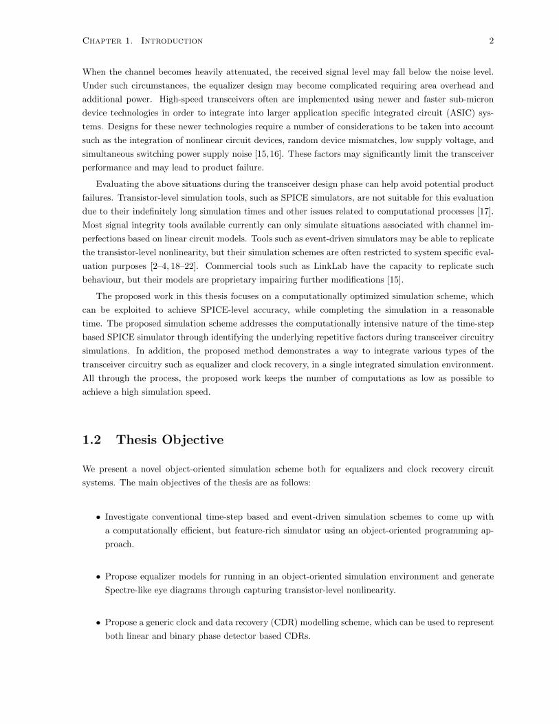
Chapter 2. Background 5
Signal
InCrosstalk
Signal
Out
Package
Chip
Pad Pad
ViaConductor
· · ·
· · · ︷︷ ︸Transmitter
︸ ︷︷ · · ·ReceiverBond-wire
Figure 2.1: A schematic of a typical channel construction
to chip pad takes place. The signal leaving the trasmitter chip often travels through several connectors,
such as vias and bond-wires. In addition, unwanted signal fragments may appear from neighbouring
data transmission lines.
The communication channel, such as the one shown above, suffers from three major problems: signal
attenuation, reflection, and cross-talk [15]. Signal attenuation occurs mostly due to conductor and
dielectric loss. Signal reflection is caused by impedance discontinuities in the channel. An impedance
discontinuity exists, whenever the signal path changes from one material layer to another, such as at the
interface between pads, bond-wires, and vias. Crosstalk occurs due to neighbouring data transmission
channels. As a product form-factor gets smaller over time, the transmission system often suffers from
crosstalk at various locations. Depending on the crosstalk location and strength, it may limit the signal
transmission speed.
Another source of signal integrity is semiconductor device nonlinearity. As the data transmission
frequency goes up, smaller sub-micron semiconductor devices are used to design transceiver circuitry
due to their higher terminal frequencies and lower power consumption. Designing transceivers in smaller
devices also allows for integration with other large compact ASIC systems such as microprocessors and
memory. Using smaller devices can cause a wide variety of other signal integrity issues, such as nonlinear
transistor characteristics, random device mismatches, process variation and power supply noise. For
instance, device-level nonlinearity, process variation, and random device mismatches affect linearity of
transceiver filter operations. Power supply noise, which is mostly due to digital system integration,
escalates noise-level during the data transmission and increases the BER.
2.2 Serial Link Transceiver Architecture
Depending on the data transmission rate and channel characteristics, the transceiver architecture must
vary in complexity to counteract the unwanted noise and interference. An objective of the transceiver
operation is to minimize the probability of data transmission error while maintaining low power consump-
tion and a small footprint. Having a low BER is certainly desirable to achieve high data transmission
efficiency. Low power consumption is important in order to keep the overall system power within the
budget.
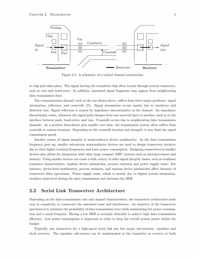
Typically, any transceiver for a high-speed serial link has two major sub-systems: equalizer and
clock recovery. The equalizer sub-system can be implemented at the trasmitter or receiver or both

Chapter 2. Background 6
Transmitter Receiver
Source TxEQ Ch RxEQ Sink
TxClk
RxClk
Clock
Recovery
Figure 2.2: Generic transceiver architecture for high-speed serial links
ends depending on the channel attenuation level. If the channel is highly attenuating, equalization is
performed at the both ends. The clock recovery, which is an essential for providing the clock in order to
sample at the optimum signal location, is implemented at the receiver.
Figure 2.2 shows a typical construction of a transceiver. The source generates data synchronized
to the clock at the trasmitter (marked by TxClk). Input data is then equalized by the equalizer at
the trasmitter (shown as TxEQ) before transmitting through the channel (shown as Ch). Once the
signal through the channel arrives at the receiver, the equalizer at the receiver (shown as RxEQ) further
equalizes the signal to prepare it for sampling. The clock recovery unit generates clock signal (marked
as RxClk) for sampling the transmitted data. It determines the optimal sampling phase by analyzing
previously detected samples from the RxEQ. It is worth mentioning that both equalizers depending on
their architectures require clocking in order to perform equalization.
Conceptual details of both equalizer and clock recovery units are described in sections 2.2.1 and 2.2.2
respectively.
2.2.1 Equalization Overview
Equalization inverts the transmitted symbol distortion caused in a channel at high frequency [25]. By
nature, any channel behaves like a passive low pass filter. For wire-line communication, the frequency
content of a transmitted bit-stream usually ranges from 0 Hz to all the way up to Nyquist frequency,
fN (i.e. fN = fBit−Rate/2). When a random bit-stream is transmitted through a channel at a high rate,
the higher frequency content of the transmitted bits get attenuated and delayed compared to those at
lower frequencies. This low pass filtering behaviour of the channel introduces ISI, because transmitted
current bits are affected by both previous and later transmitted bits. The task of an equalizer is to
reduce the amount of ISI to an acceptable minimum level so that transmitted symbols can be exactly
reconstructed after sampling.
Equalizers for any high-speed serial link can be realized using two main approaches: frequency domain
and time domain. Both approaches are shown in Figure 2.3. In all sub-figures, vertical axes represent
the amplitudes, while horizontal axis is either frequency, ω, (in sub-figure (a)) or time, t, (in sub-figure
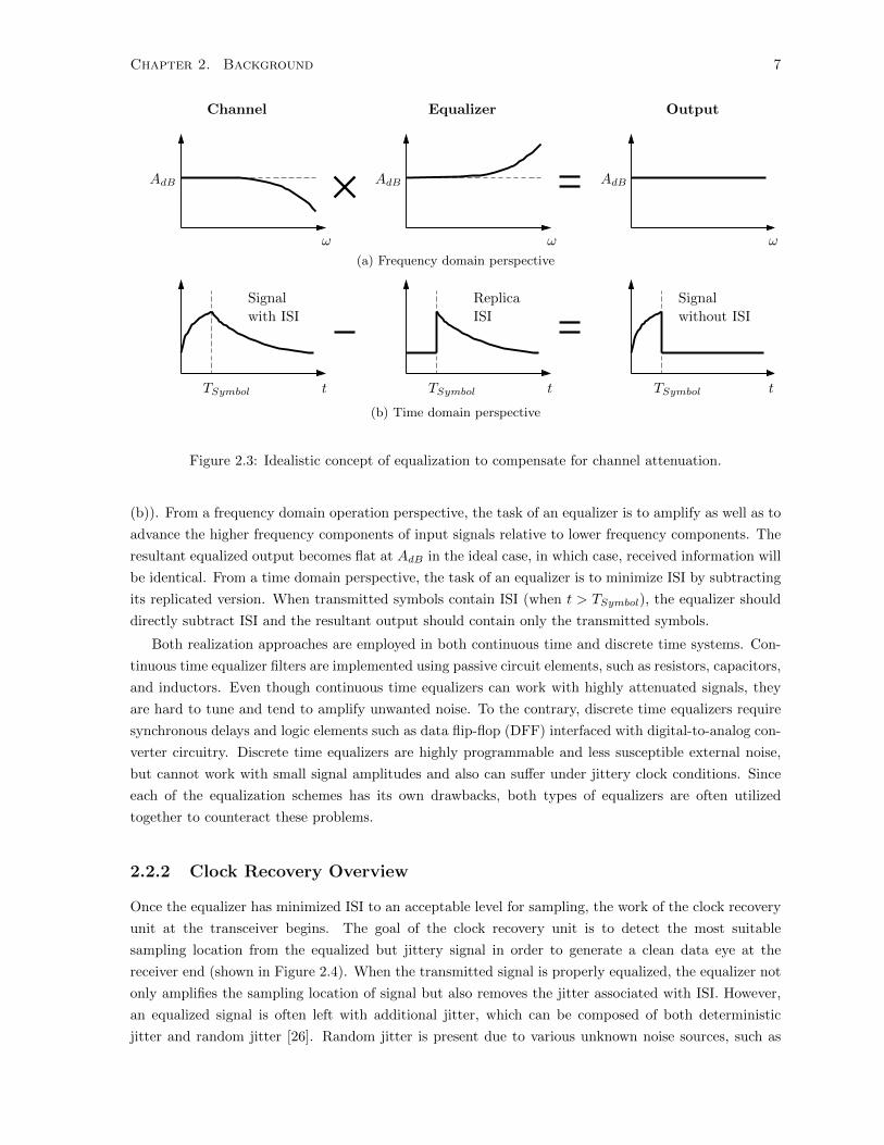
Chapter 2. Background 7
Channel Equalizer Output
ω ω ω
AdB AdB AdB
(a) Frequency domain perspective
Signal
with ISI
Replica
ISI
Signal
without ISI
t t tTSymbol TSymbol TSymbol
(b) Time domain perspective
Figure 2.3: Idealistic concept of equalization to compensate for channel attenuation.
(b)). From a frequency domain operation perspective, the task of an equalizer is to amplify as well as to
advance the higher frequency components of input signals relative to lower frequency components. The
resultant equalized output becomes flat at AdB in the ideal case, in which case, received information will
be identical. From a time domain perspective, the task of an equalizer is to minimize ISI by subtracting
its replicated version. When transmitted symbols contain ISI (when t > TSymbol), the equalizer should
directly subtract ISI and the resultant output should contain only the transmitted symbols.
Both realization approaches are employed in both continuous time and discrete time systems. Con-
tinuous time equalizer filters are implemented using passive circuit elements, such as resistors, capacitors,
and inductors. Even though continuous time equalizers can work with highly attenuated signals, they
are hard to tune and tend to amplify unwanted noise. To the contrary, discrete time equalizers require
synchronous delays and logic elements such as data flip-flop (DFF) interfaced with digital-to-analog con-
verter circuitry. Discrete time equalizers are highly programmable and less susceptible external noise,
but cannot work with small signal amplitudes and also can suffer under jittery clock conditions. Since
each of the equalization schemes has its own drawbacks, both types of equalizers are often utilized
together to counteract these problems.
2.2.2 Clock Recovery Overview
Once the equalizer has minimized ISI to an acceptable level for sampling, the work of the clock recovery
unit at the transceiver begins. The goal of the clock recovery unit is to detect the most suitable
sampling location from the equalized but jittery signal in order to generate a clean data eye at the
receiver end (shown in Figure 2.4). When the transmitted signal is properly equalized, the equalizer not
only amplifies the sampling location of signal but also removes the jitter associated with ISI. However,
an equalized signal is often left with additional jitter, which can be composed of both deterministic
jitter and random jitter [26]. Random jitter is present due to various unknown noise sources, such as
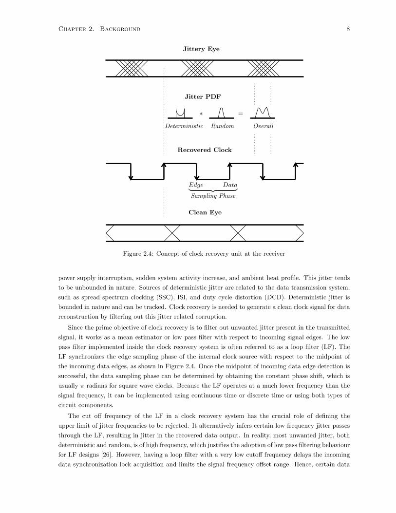
Chapter 2. Background 8
Jittery Eye
Jitter PDF
∗ =
Deterministic Random Overall
Recovered Clock
Edge Data︸ ︷︷ ︸Sampling Phase
Clean Eye
Figure 2.4: Concept of clock recovery unit at the receiver
power supply interruption, sudden system activity increase, and ambient heat profile. This jitter tends
to be unbounded in nature. Sources of deterministic jitter are related to the data transmission system,
such as spread spectrum clocking (SSC), ISI, and duty cycle distortion (DCD). Deterministic jitter is
bounded in nature and can be tracked. Clock recovery is needed to generate a clean clock signal for data
reconstruction by filtering out this jitter related corruption.
Since the prime objective of clock recovery is to filter out unwanted jitter present in the transmitted
signal, it works as a mean estimator or low pass filter with respect to incoming signal edges. The low
pass filter implemented inside the clock recovery system is often referred to as a loop filter (LF). The
LF synchronizes the edge sampling phase of the internal clock source with respect to the midpoint of
the incoming data edges, as shown in Figure 2.4. Once the midpoint of incoming data edge detection is
successful, the data sampling phase can be determined by obtaining the constant phase shift, which is
usually π radians for square wave clocks. Because the LF operates at a much lower frequency than the
signal frequency, it can be implemented using continuous time or discrete time or using both types of
circuit components.
The cut off frequency of the LF in a clock recovery system has the crucial role of defining the
upper limit of jitter frequencies to be rejected. It alternatively infers certain low frequency jitter passes
through the LF, resulting in jitter in the recovered data output. In reality, most unwanted jitter, both
deterministic and random, is of high frequency, which justifies the adoption of low pass filtering behaviour
for LF designs [26]. However, having a loop filter with a very low cutoff frequency delays the incoming
data synchronization lock acquisition and limits the signal frequency offset range. Hence, certain data
Chapter 2. Background 9
transceiver applications must be adapted for certain cutoff frequencies of the LF, depending on the
nature of the jitter probability density function (PDF) characteristics and system design specifications.
2.3 Performance Evaluation Criteria
Data transmission through a serial link is negatively affected by the error rate in the received data. A
high data transmission error rate increases activities associated with received data error management,
such as repeated data transmission, forward error correction, and a high density of parity bits [25]. A
high error rate not only increases overall system power consumption, but also can limit the effective
data transmission rate. In order to achieve a high data transmission rate while reducing the associated
operating power requirements, it is essential to maximize data transmission efficiency. Modern high data-
rate (10 Gbps or more) transmission applications therefore have stringent low bit error rate (10−12 −10−16) requirements [14].
Implementing systems to transmit at high data-rates while maintaining ultra-low BER becomes a
major engineering challenge. Fulfilling the challenge with respect to short time-frame to market as well
as high manufacturing cost for modern sub-micron devices does not permit iterative manufacturing and
testing on the laboratory environment. Instead, it is preferable to perform system-level verification tests
via simulations. Simulator-based verification facilitates the design and evaluation of multiple types of
transceiver architectures at the pre-manufacturing stage. Two popular system verification approaches,
BER eye diagram and jitter tolerance, are discussed as follows.
2.3.1 Bit-Error-Rate (BER) Eye Diagrams
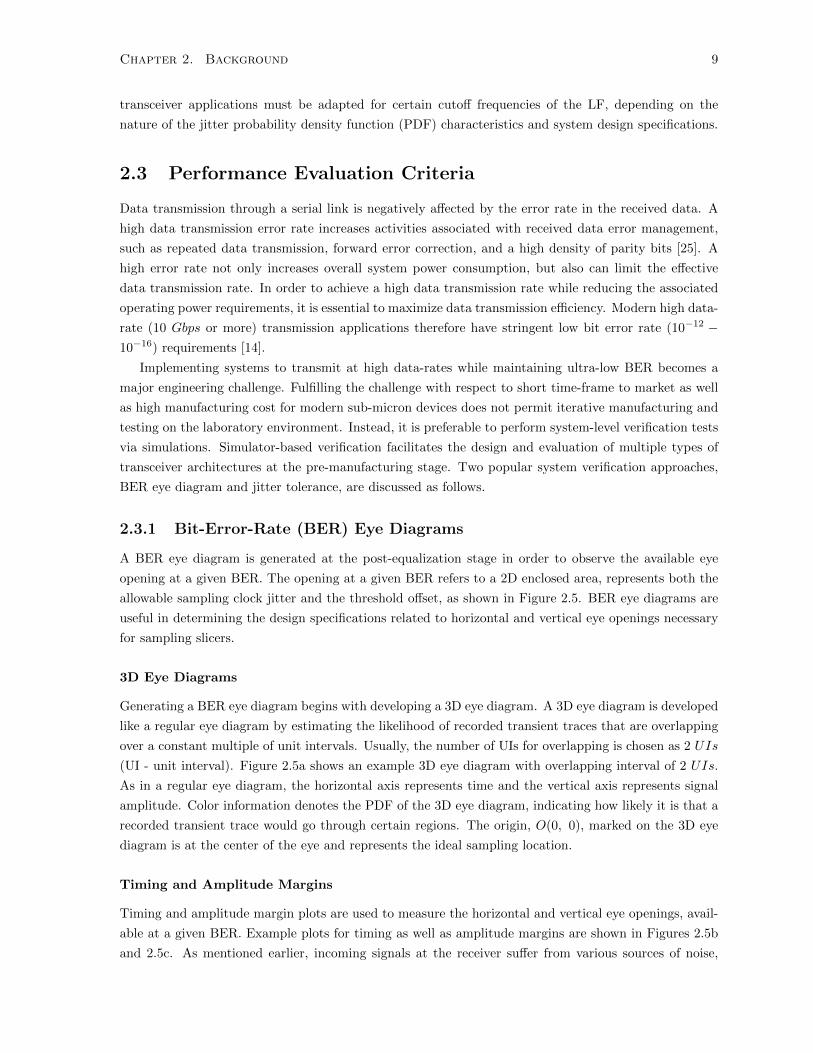
A BER eye diagram is generated at the post-equalization stage in order to observe the available eye
opening at a given BER. The opening at a given BER refers to a 2D enclosed area, represents both the
allowable sampling clock jitter and the threshold offset, as shown in Figure 2.5. BER eye diagrams are
useful in determining the design specifications related to horizontal and vertical eye openings necessary
for sampling slicers.
3D Eye Diagrams
Generating a BER eye diagram begins with developing a 3D eye diagram. A 3D eye diagram is developed
like a regular eye diagram by estimating the likelihood of recorded transient traces that are overlapping
over a constant multiple of unit intervals. Usually, the number of UIs for overlapping is chosen as 2 UIs
(UI - unit interval). Figure 2.5a shows an example 3D eye diagram with overlapping interval of 2 UIs.
As in a regular eye diagram, the horizontal axis represents time and the vertical axis represents signal
amplitude. Color information denotes the PDF of the 3D eye diagram, indicating how likely it is that a
recorded transient trace would go through certain regions. The origin, O(0, 0), marked on the 3D eye
diagram is at the center of the eye and represents the ideal sampling location.
Timing and Amplitude Margins
Timing and amplitude margin plots are used to measure the horizontal and vertical eye openings, avail-
able at a given BER. Example plots for timing as well as amplitude margins are shown in Figures 2.5b
and 2.5c. As mentioned earlier, incoming signals at the receiver suffer from various sources of noise,

Chapter 2. Background 10
3D Eye Diagram
Am
pli
tud
e
Time (UI)
O
Origin, O(0, 0)
PD
F
High
Low
(a)
Timing Margin
log10BER
Time (UI)
(b)
Amplitude Margin
Am
pli
tud
e
log10BER
(c)
3D BER Eye
Am
pli
tud
e
Time (UI)
log10BER
High
Low
(d)
BER Contour
Am
pli
tud
e
Time (UI)
High
Low
(e)
Figure 2.5: Concept of generating a bit error rate (BER) eye diagram
Chapter 2. Background 11
which can be categorized as either deterministic or random noise. Effects of both deterministic and
random noise are visible in the margin plots: deterministic noise causes flat regions, whereas random
noise leads to gradually declining margins, as the BER is reduced logarithmically. A timing margin plot
can be generated from the eye diagram by integrating the measured PDF across the zero-crossing level,
shown in Figure 2.5a, as horizontal dotted line passes through the origin. Similarly, voltage margin plots
can be obtained by integrating the PDF vertically while sampling from the origin.
Even though both timing and amplitude margin plots infer how much eye opening can be obtained
at a specific BER, they have their own drawbacks due to their underlying assumptions. Timing margin
plots assume the data being sliced exactly with respect to the zero-cross level. Similarly, amplitude
margin plots provide the amount of vertical opening under the assumption that the sampling clock (or
recovered clock) has no jitter. In reality, the data slicer and the sampling clock are never perfect, so
amplitude and timing margins cannot be considered independent from each other.
BER Eye Diagram and its Contour Map
When the 3D eye diagram is integrated over its 2D time-amplitude plane, the resultant 3D plot contains
cumulative distribution function (CDF) information of the overlapped transient traces. This 3D CDF
plot is also called a 3D BER eye (Figure 2.5d). It can be observed based on the logarithmically scaled
colour bar in Figure 2.5d: as sampling time and slicer threshold shift away from the origin, O(0, 0),
over the 2D plane, the probability of error increases. The white space located in the center of the BER
plot represents log 0 = −∞, since no transient plot passes through the region.
From the 3D BER eye plot, the BER contour can be interpolated (or extrapolated) using regional
3D slope information at a user specified BER value (Figure 2.5e). In the BER contour plot, each
contour outlines an area that represents both on acceptable sampling clock jitter and slicer threshold
variation. As expected from the figure, lower BER contours cover a smaller area. In order for the data
transmission system to meet specific BER requirements, receiver recovered clock jitter as well as slicer
threshold nonlinear variations must be jointly limited within the specified BER contour boundary. It can
be inferred from the contour properties that timing and voltage margins are not considered separately,
and therefore, it is the best way to perform serial link verification.
2.3.2 Jitter Tolerance
Even though BER eye diagrams can provide information about the best timing margins for sampling,
they can be used only to evaluate the actual allowable high frequency jitter for a clock recovery system.
Certain low frequency jitters, such as SSC-related jitter, can have a timing spread of more than 1 UI,
which can easily lead to closed eye diagrams and zero timing margins. Evaluating a serial link under
such circumstance requires the performance of a jitter tolerance test for the clock recovery unit. A jitter
tolerance test can also be used to analyze the jitter frequency characteristic of the clock recovery unit,
particularly of the LF. As explained in Section 2.2.2, the LF defines the key jitter cutoff frequency, which
is not only responsible for output jitter in recovered data but also relevant to data synchronization lock
time.
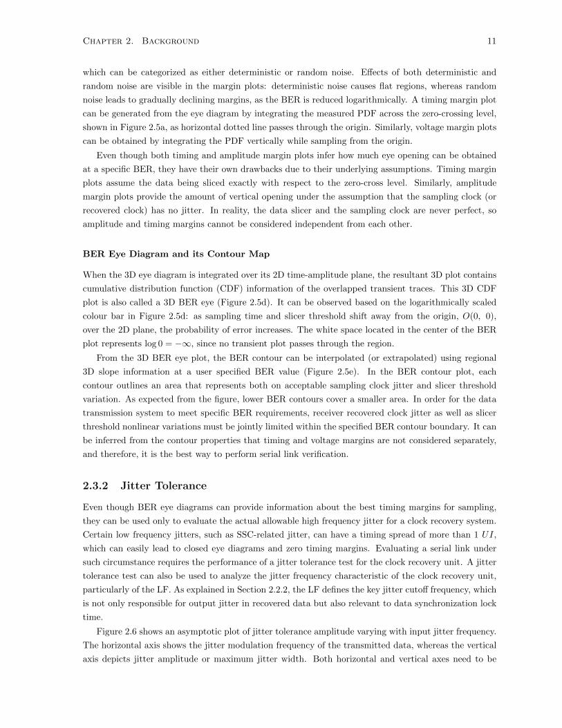
Figure 2.6 shows an asymptotic plot of jitter tolerance amplitude varying with input jitter frequency.
The horizontal axis shows the jitter modulation frequency of the transmitted data, whereas the vertical
axis depicts jitter amplitude or maximum jitter width. Both horizontal and vertical axes need to be

Chapter 2. Background 12
Jitter Tolerance
log10 Amplitude
≤ 1 UI
−40 dB/decade
0 Hz ← fj f
log10 Frequency
Figure 2.6: Asymptotic jitter tolerance plot
distributed logarithmically in order to capture wide range values. Initially, transmitted data is usually
modulated with sinusoidal jitter at a given frequency. Then the amplitude of the sinusoidal jitter is
increased in order to search for the transition amplitude, up to which point the clock recovery system
can track without making any detection error. The searching procedure needs to take into account
the initial synchronization lock acquisition period and its associated detection errors the clock recovery
system would make. As can be observed from the figure, at low input jitter frequencies (0 Hz < f < fj),
jitter amplitude tolerance for the recovery system increases, since the LF allows low frequency jitter to
pass through the system. At high input jitter frequencies (when f ≥ fj), jitter amplitude tolerance
reaches a constant limit, ≤ 1 UI, as the jitter frequency goes beyond the trackable limit of LF. At
low jitter frequencies, the jitter tolerance amplitude generally increases at a constant rate. The slope
varies depending on the clock recovery system architecture. For second-order phase tracking based clock
recovery systems, the slope is 40 dB/decade. (Details on generating a jitter tolerance plot can be found
in the Appendix A of [27].)
2.4 Analog-Mixed Signal (AMS) Simulation Overview
The objective of AMS simulation is to simulate discrete time components alongside continuous time
components. Simulating continuous time circuit components, such as resistive-capacitive filters, passive
equalizers, and amplifiers, is highly demanding of computational resources due to the sophisticated mod-
elling systems required. Performing top-level verification of a reasonably sized AMS system of current
applications is therefore usually impractical, if only continuous time models for all circuit blocks are
employed. Since analog circuitry requires careful performance evaluation due to its complex behaviour,
modelling analog circuits with continuous time modelling is justifiable. To the contrary, because sim-
ulations of digital systems are usually performed to ensure logical correctness, computationally light
discrete time modelling is sufficient. AMS simulators therefore have great significance for various top-
level verification processes.
AMS simulators are mainly used for system-level transient simulation purposes. There are two ways
Chapter 2. Background 13
to perform AMS simulations: time-step based and event-driven simulations. Working principles for
most commercial AMS simulators follow time-step based simulation due to its close resemblance to and
easy adaption of continuous time circuitry simulation schemes. Recently, event-driven simulation has
become increasingly popular in research communities due to its speed advantages over time-step based
simulation. Details for both schemes are described below.
2.4.1 Time-Step Based Simulation
Time-step based simulation is specifically designed for simulating analog circuit components to capture
their continuous time and nonlinear behaviour with high accuracy. The basic concept of time-step based
simulation is to calculate the output of the next time step based on the input as well as the output of the
current step. Time-step based simulator therefore usually employs circuit components modelled with
an ordinary differential equation (ODE) based scheme (Section 2.5.1). In time-step based simulations,
outputs of continuous-time circuit components are evaluated at discrete time-steps. Accuracy of the
continuous-time output calculations depends on the granularity of the chosen time-steps. Conducting a
simulation with smaller time-steps increases simulation time, whereas larger time-steps reduce accuracy
and leads to potential convergence instability [18, 22, 28]. Therefore, picking the right time-steps is
critical for this type of simulation scheme.
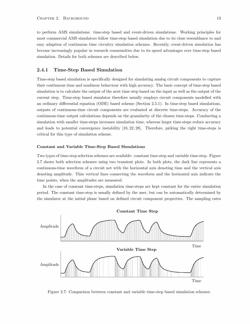
Constant and Variable Time-Step Based Simulations
Two types of time-step selection schemes are available: constant time-step and variable time-step. Figure
2.7 shows both selection schemes using two transient plots. In both plots, the dark line represents a
continuous-time waveform of a circuit net with the horizontal axis denoting time and the vertical axis
denoting amplitude. Thin vertical lines connecting the waveform and the horizontal axis indicate the
time points, when the amplitudes are measured.
In the case of constant time-steps, simulation time-steps are kept constant for the entire simulation
period. The constant time-step is usually defined by the user, but can be automatically determined by
the simulator at the initial phase based on defined circuit component properties. The sampling rates
Constant Time Step
Amplitude
TimeVariable Time Step
Amplitude
Time
Figure 2.7: Comparison between constant and variable time-step based simulation schemes
Chapter 2. Background 14
associated with the simulation time-steps must be greater than or equal to twice of the maximum circuit
system operating frequency in order to perform exact reconstruction without aliasing, according to the
Nyquist-Shannon Sampling theorem. In practice, the sampling rate should be about 10−15 times of the
maximum operating frequency, because outputs at the non-measured time points are usually interpolated
based on the neighbouring measured time points [29]. In order to maintain the expected accuracy during
the interpolation process, the suggested sampling rate is sufficient for most cases.
Having a constant time-step based simulation scheme is inefficient, since the simulator is blindly
picking time points regardless of observable activity. Variable time-step based simulations are therefore
preferable, since the simulation time-steps are picked based on circuit activity, specifically based on the
slope of the signal amplitude. Whenever the signal has steeper slopes, smaller time-steps are picked,
and whenever the signal has flatter slopes, larger time-steps are picked.
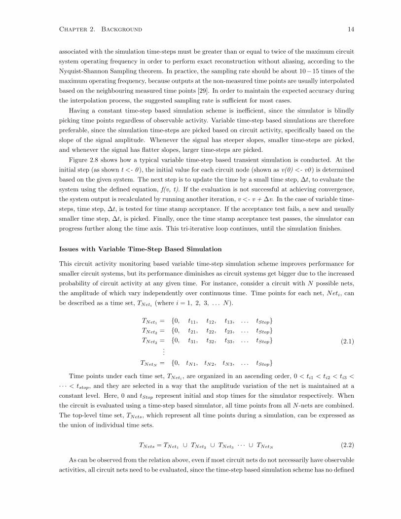
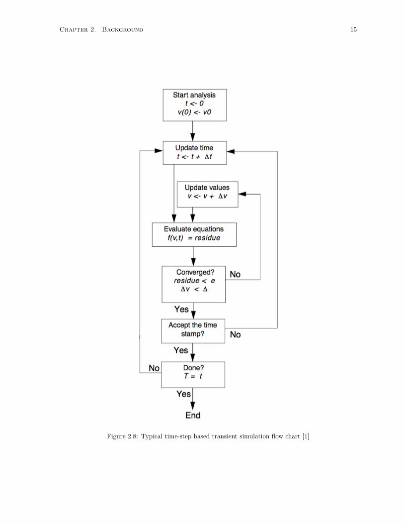
Figure 2.8 shows how a typical variable time-step based transient simulation is conducted. At the
initial step (as shown t <- 0 ), the initial value for each circuit node (shown as v(0) <- v0 ) is determined
based on the given system. The next step is to update the time by a small time step, ∆t, to evaluate the
system using the defined equation, f(v, t). If the evaluation is not successful at achieving convergence,
the system output is recalculated by running another iteration, v <- v + ∆v. In the case of variable time-
steps, time step, ∆t, is tested for time stamp acceptance. If the acceptance test fails, a new and usually
smaller time step, ∆t, is picked. Finally, once the time stamp acceptance test passes, the simulator can
progress further along the time axis. This tri-iterative loop continues, until the simulation finishes.
Issues with Variable Time-Step Based Simulation
This circuit activity monitoring based variable time-step simulation scheme improves performance for
smaller circuit systems, but its performance diminishes as circuit systems get bigger due to the increased
probability of circuit activity at any given time. For instance, consider a circuit with N possible nets,
the amplitude of which vary independently over continuous time. Time points for each net, Neti, can
be described as a time set, TNeti (where i = 1, 2, 3, . . . N).
TNet1 = 0, t11, t12, t13, . . . tStopTNet2 = 0, t21, t22, t23, . . . tStopTNet2 = 0, t31, t32, t33, . . . tStop
...
TNetN = 0, tN1, tN2, tN3, . . . tStop
(2.1)
Time points under each time set, TNeti , are organized in an ascending order, 0 < ti1 < ti2 < ti3 <
· · · < tstop, and they are selected in a way that the amplitude variation of the net is maintained at a
constant level. Here, 0 and tStop represent initial and stop times for the simulator respectively. When
the circuit is evaluated using a time-step based simulator, all time points from all N -nets are combined.
The top-level time set, TNets, which represent all time points during a simulation, can be expressed as
the union of individual time sets.
TNets = TNet1 ∪ TNet2 ∪ TNet3 · · · ∪ TNetN (2.2)
As can be observed from the relation above, even if most circuit nets do not necessarily have observable
activities, all circuit nets need to be evaluated, since the time-step based simulation scheme has no defined
Chapter 2. Background 15
Figure 2.8: Typical time-step based transient simulation flow chart [1]

Chapter 2. Background 16
way to isolate the nets without observable activities. Hence, as circuit size grows, the time point density
increases in TNets due to the increased probability of circuit activities, decreasing the benefits of variable
time-step based simulations.
2.4.2 Event-Driven Simulation
Event-driven programming was initially developed for graphical user interface (GUI) based application
software [30]. Once any GUI based application is launched, the software executes commands whenever
a user interacts with it and sleeps otherwise. This brings significant efficiency in software operation. A
similar idea was adopted for simulating digital circuit system, because digital circuitry remains at one
of its amplitude levels associated with a binary logical state of either logic 0 or 1 majority of the time,
although it is built using transistors, as in analog circuitry. Whenever any digital circuit block needs
to be evaluated, events are scheduled in the event queue and the simulator executes circuit blocks in
the ascending order of event time stamps. This type of simulator is optimized not only along the time
axis like variable time-steps, but also across system space. The time axis and system space optimization
property is referred to as spatiotemporal optimization. Due to such property, event-driven simulation
provides significant speed advantages and computational efficiency in comparison with time-step based
simulation, even for large-scale systems.
As in digital systems, any high-speed serial link communication involves a digital source at the
trasmitter and a digital sink at the receiver (Figure 2.2). The digital source, which is synchronous with
the trasmitter clock, usually generates a random discrete signal stream mimicking the properties of the
transition density of actual sources. Similarly, the digital sink, synchronized with the receiver clock,
samples the transmitted digital signal. Figure 2.9 shows an example case, where a simple transceiver
operation is simulated. In the example, the event scheduler receives the next transition events from
TX and CDR using their corresponding event routines. The task of the event scheduler is to sort out
Figure 2.9: Concept of event driven simulation: (a) block diagram, (b) operation [2]
Chapter 2. Background 17
the transition events in an ascending order and activate the circuit blocks based on that order. Only
the channel and equalizers are analog, but a number of methods have been proposed to overcome the
issue to a certain extent. As a whole, event-driven simulation is becoming nearly an ideal candidate for
system-level verification of high-speed communication over serial links.
Drawbacks of event-driven simulations arise from its requirement of predicting future events for
execution. For synchronous systems, future events can be predicted using the local clock transition
interval and clock operations are relatively independent from external effects. For instance, if a system
has a binary phase detector (PD)-based CDR, future transition events of its VCO can be calculated in
advance based on the current state of binary PD. Synchronous circuit blocks, which are connected to
such CDRs, can simply refer to the time-events of the CDR. However, this non-causal behaviour cannot
be applied to asynchronous circuit blocks, such as slicer or linear PD. Since these asynchronous circuit
blocks work based on zero-crossing detection and the zero-crossing detection requires time-step based
waveforms, events associated with zero-crossing cannot be estimated without going over the time-step
based waveforms.
2.5 Modelling for Continuous Time Component Blocks
The key challenges of conducting an AMS simulation come from modelling continuous time circuit
blocks. Modelling a continuous time circuit block is always challenging, because its output varies both
in time and amplitude. Since computation can be performed in discrete time, time points for continuous
time output calculations are determined based on the system defining properties. For example, if an
operational amplifier is tested in transient mode for continuous time input amplification, time points
should be placed as closely as possible. In that case, it is preferable to adopt a state-space based modelling
scheme in time-step based simulation environment. However, if a switch capacitor-based circuit needs to
be tested, it is usually necessary to observe outputs at each clock transition. Under such circumstances,
it is preferable to adopt a continuous time modelling scheme, which can be used to calculate output
in any given time space. Here, four popular and recently developed modelling schemes applicable for
continuous time circuitry from transceiver operation perspective are presented.
2.5.1 Ordinary Differential Equation (ODE) Based Modelling
ODE-based modelling for continuous-time circuitry is the most popular scheme implemented in major
commercial simulators due to its versatility in device-level nonlinear modelling and generalizability in
any circuit analysis. This modelling scheme is mainly adopted in time-step based simulation schemes,
as mentioned earlier in Section 2.4.1. Modelling in ODE-based schemes is usually based on modified
nodal analysis (MNA), because most nonlinear circuit devices are modelled using controlled current
sources [1, 28]. A generic form of the equation for a node can be written based on Kirchhoff’s law on
currents (KCL), as shown in Figure 2.10.
Figure 2.10 shows all possible circuit branches connected to a node. Each circuit branch contains a
two-terminal load, which is shown as a rectangular box. Current through each branch is quantified as,
in(v, t)+Kn ·dqn(v, t)
dt, where Kn represents respective gain coefficient and n denotes the branch index.
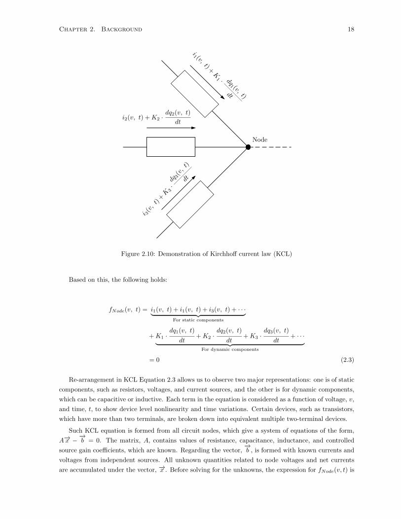
Chapter 2. Background 18
Node
i1 (v,t) +
K1 · dq
1 (v,t)dt
i2(v, t) +K2 ·dq2(v, t)
dt
i 3(v,t)
+K 3·dq
3(v,t)
dt
Figure 2.10: Demonstration of Kirchhoff current law (KCL)
Based on this, the following holds:
fNode(v, t) = i1(v, t) + i1(v, t) + i3(v, t) + · · ·︸ ︷︷ ︸For static components
+K1 ·dq1(v, t)
dt+K2 ·
dq2(v, t)
dt+K3 ·
dq3(v, t)
dt+ · · ·︸ ︷︷ ︸
For dynamic components
= 0 (2.3)
Re-arrangement in KCL Equation 2.3 allows us to observe two major representations: one is of static
components, such as resistors, voltages, and current sources, and the other is for dynamic components,
which can be capacitive or inductive. Each term in the equation is considered as a function of voltage, v,
and time, t, to show device level nonlinearity and time variations. Certain devices, such as transistors,
which have more than two terminals, are broken down into equivalent multiple two-terminal devices.
Such KCL equation is formed from all circuit nodes, which give a system of equations of the form,
A−→x −−→b = 0. The matrix, A, contains values of resistance, capacitance, inductance, and controlled
source gain coefficients, which are known. Regarding the vector,−→b , is formed with known currents and
voltages from independent sources. All unknown quantities related to node voltages and net currents
are accumulated under the vector, −→x . Before solving for the unknowns, the expression for fNode(v, t) is

Chapter 2. Background 19
further simplified by applying finite difference approximation: as in any derivative entity of y, dy/dt ≈(y(t+∆t)−y(t))/∆t, where ∆t represents appropriately selected time-steps based on system convergence
requirements. This allows us to linearize the system before solving it algebraically.
The system of equations can now be solved directly by inverting the matrix, or iteratively through
making an initial guess. Even though the direct inversion method can be adopted for smaller circuit
systems, the iterative approach is usually preferred to maximize the processing capability for solving
large circuit systems. Among various iterative solving methods, Newton-Raphson’s method (NR) is
one of the most commonly applied methods. Equation 2.4 describes the iterative approach of the NR
method:
xn+1 = xn −f(xn)
f ′(xn)(2.4)
en+1 = (xn+1 − xn) ≤MaxRelTol(xn+1), AbsTol (2.5)
As can be seen from Equation 2.4, a function, f(xn) can be solved, if there exists a non-zero first-
order derivative f ′(xn) 6= 0. Since the circuit system is usually nonlinear and dynamic in nature, its
system of equations satisfies the required conditions for the NR method. After obtaining the new value
xn+1 through applying xn, the error for the new value, en+1, can be calculated, as shown in Equation
2.5. For every new value of xn, the corresponding error en+1 is estimated, and the error value, en+1
goes down, as the number of iterations is increased. It also worth mentioning that during every new
iteration, new operating points for all nonlinear circuit components need to be obtained meaning that
the system of equations changes for every new error value, en+1.
The process of iterations continues until the error value drops below a preset simulation error limit.
The preset error limit is the maximum of relative error (referred as RelTol) and absolute error (referred
as AbsTol), as shown in the equation. Relative error is defined as a function of the new value, xn+1,
through the relation, RelTol(xn+1) = |xn+1−xn|/Minxn+1, xn. When the value is much larger than
zero (xn 0), relative error is signified during error calculation. However, without absolute tolerance,
it is not possible to achieve convergence using the NR method. For systems of equations, multiple
error values would need to be calculated for multiple circuit nodes. In such cases, the maximum of all
calculated error values is used for error limit comparison.
It can be inferred from the above discussion that the ODE based modelling scheme allows us to use
any arbitrary input signal, since the output for each circuit node is calculated at every time point. It can
also be clearly seen that the calculation scheme is significantly computationally intensive. As the system
size grows, the system of equations (which is a square matrix in order to have a unique solution set) grows
and matrix inversion complexity increases nearly exponentially. Determining the initial guess, x0, can be
troublesome, because the system needs to intelligently pick the values to ensure convergence; otherwise,
the initial guess needs to be provided manually for each circuit node by the user. Convergence failure
can also arise from not selecting the proper time step, ∆t. Like the case of larger time steps leading to
larger errors, certain continuous functions, such as tanh(x), which do not always have finite derivative,
may often cause convergence failure due to improper time point selection.
Chapter 2. Background 20
2.5.2 Pulse Response Based Modelling
Modelling continuous time circuit behaviour using pulse responses requires representing the transmitted
binary signal through a summing input pulse train multiplied by the transmitted symbols. This is one
of the continuous time component modelling techniques, whose operation principles closely resemble
the event-driven simulation scheme. The modelling scheme is also employed to generate statistical
eye diagrams, a technique which can be used to create eye diagrams with integrated statistical PDF
information without running time-consuming transient simulations [31]. The rest of the section explains
the core concept of how to generate continuous-time output waveform applying the recorded pulse
response.
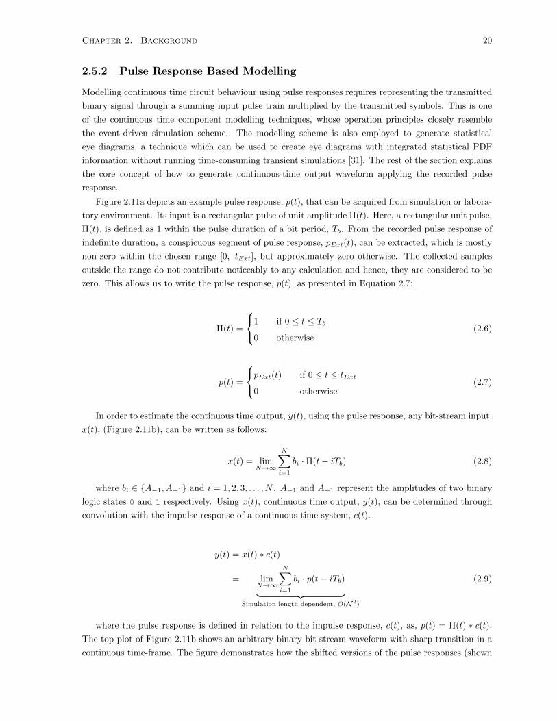
Figure 2.11a depicts an example pulse response, p(t), that can be acquired from simulation or labora-
tory environment. Its input is a rectangular pulse of unit amplitude Π(t). Here, a rectangular unit pulse,
Π(t), is defined as 1 within the pulse duration of a bit period, Tb. From the recorded pulse response of
indefinite duration, a conspicuous segment of pulse response, pExt(t), can be extracted, which is mostly
non-zero within the chosen range [0, tExt], but approximately zero otherwise. The collected samples
outside the range do not contribute noticeably to any calculation and hence, they are considered to be
zero. This allows us to write the pulse response, p(t), as presented in Equation 2.7:
Π(t) =
1 if 0 ≤ t ≤ Tb0 otherwise
(2.6)
p(t) =
pExt(t) if 0 ≤ t ≤ tExt0 otherwise
(2.7)
In order to estimate the continuous time output, y(t), using the pulse response, any bit-stream input,
x(t), (Figure 2.11b), can be written as follows:
x(t) = limN→∞
N∑i=1
bi ·Π(t− iTb) (2.8)
where bi ∈ A−1, A+1 and i = 1, 2, 3, . . . , N . A−1 and A+1 represent the amplitudes of two binary
logic states 0 and 1 respectively. Using x(t), continuous time output, y(t), can be determined through
convolution with the impulse response of a continuous time system, c(t).
y(t) = x(t) ∗ c(t)
= limN→∞
N∑i=1
bi · p(t− iTb)︸ ︷︷ ︸Simulation length dependent, O(N 2)
(2.9)
where the pulse response is defined in relation to the impulse response, c(t), as, p(t) = Π(t) ∗ c(t).The top plot of Figure 2.11b shows an arbitrary binary bit-stream waveform with sharp transition in a
continuous time-frame. The figure demonstrates how the shifted versions of the pulse responses (shown

Chapter 2. Background 21
t0 tExt
p(t)
0
1Extracted SegmentpExt(t)
(a) Pulse response extraction
Random Bit-stream, x(t)
tTb 2Tb 3Tb 4Tb · · ·
A+1
A−1
Shifted Pulse Responses, bi · pExt(t− iTb)...
t
t
t
Tb 2Tb
2Tb 3Tb
3Tb 4Tb
0
0
0
A+1
A−1
A−1
...
Summed Step Response, y(t)
t
A+1
A−1
(b) Waveform formation
Figure 2.11: Continuous time waveform formation using pulse-response based modelling

Chapter 2. Background 22
in the middle section) are summed to generate the desired output response, y(t) (shown in the bottom
section).
As can be seen in Equation 2.9, the summation must be executed for all transmitted bits throughout
the entire simulation. Due to these facts, the complexity of the implemented algorithm for an N -bit
long simulation grows with O(N 2). In other words, simulation time grows quadratically, without even
considering computational storage requirements, which is undesirable. To bring the complexity to O(N ),
the definition of pulse response, p(t), presented in Equation 2.7, is exploited to reduce the number of
transmitted bits to be summed to a constant. In that case, the equation for calculating continuous-time
output, y(t), becomes,
y(t) = limN→∞
N∑i=N−k+1
bi · pExt(t− iTb)︸ ︷︷ ︸Simulation length independent, O(N )
(2.10)
One of the major concerns regarding Equation 2.10 is that the summation needs to be executed at
every fixed bit duration, Tb. In reality, a transmitted bit-stream often contains various effects, such as
clock jitter and amplitude variation due to equalizer effects, such as feed forward equalizer (FFE), so
the system does not always behave with realizable linearity. Capturing such behaviour requires pulse
responses of various amplitudes as well as durations, and this can make the algorithm very complex.
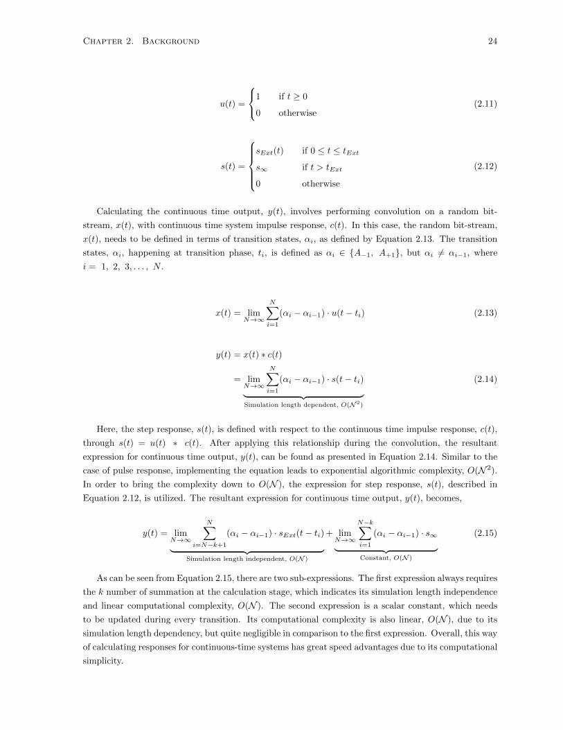
2.5.3 Step Response Based Modelling
Similar to pulse response based modelling, another continuous time modelling technique for event-driven
simulation is step response based modelling. In step response based modelling, a continuous time
waveform is estimated using the collected step response instead of the pulse response. A key advantage
of step response based modelling over pulse response based modelling is that summation needs to be
executed only when a transition occurs. Since the algorithmic summation happens during the transition
phase of transmitted bit-streams, the number of calculations is always less than or, in the worst case,
equal to that of pulse response based simulation, assuming the time vectors for both cases is of same
length. The rest of the section presents how to apply the step-response to calculate the continuous time
waveform with the aid of Figure 2.12.
The step response, s(t), is recorded for the applied unit step, u(t), as input to the continuous time
system of interest. As can be noticed from Figure 2.12a, a conspicuous segment of the step response,
sExt(t), can be extracted within the time range, [0, tExt], as in the case of pulse response, p(t). Outside
the range, the step response, s(t), is 0 at the initial stage, (when t < 0) and beyond the time range
t > tExt, s(t), it can be considered as a constant, s∞. The expression for step response, s(t), is described
in Equation 2.12.
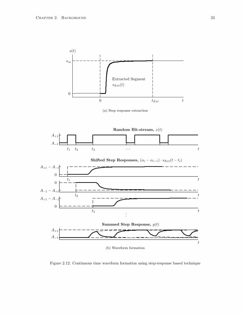
Chapter 2. Background 23
t0 tExt
s(t)
0
s∞
Extracted Segment
sExt(t)
(a) Step response extraction
Random Bit-stream, x(t)
tt1 t2 t3 · · ·
A+1
A−1
Shifted Step Responses, (αi − αi−1) · sExt(t− ti)
t
t
t
t1
t2
t3
0
0
0
A+1 −A−1
A−1 −A+1
A+1 −A−1
...
Summed Step Response, y(t)
t
A+1
A−1
(b) Waveform formation
Figure 2.12: Continuous time waveform formation using step-response based technique
Chapter 2. Background 24
u(t) =
1 if t ≥ 0
0 otherwise(2.11)
s(t) =
sExt(t) if 0 ≤ t ≤ tExts∞ if t > tExt
0 otherwise
(2.12)
Calculating the continuous time output, y(t), involves performing convolution on a random bit-
stream, x(t), with continuous time system impulse response, c(t). In this case, the random bit-stream,
x(t), needs to be defined in terms of transition states, αi, as defined by Equation 2.13. The transition
states, αi, happening at transition phase, ti, is defined as αi ∈ A−1, A+1, but αi 6= αi−1, where
i = 1, 2, 3, . . . , N .
x(t) = limN→∞
N∑i=1
(αi − αi−1) · u(t− ti) (2.13)
y(t) = x(t) ∗ c(t)
= limN→∞
N∑i=1
(αi − αi−1) · s(t− ti)︸ ︷︷ ︸Simulation length dependent, O(N 2)
(2.14)
Here, the step response, s(t), is defined with respect to the continuous time impulse response, c(t),
through s(t) = u(t) ∗ c(t). After applying this relationship during the convolution, the resultant
expression for continuous time output, y(t), can be found as presented in Equation 2.14. Similar to the
case of pulse response, implementing the equation leads to exponential algorithmic complexity, O(N 2).
In order to bring the complexity down to O(N ), the expression for step response, s(t), described in
Equation 2.12, is utilized. The resultant expression for continuous time output, y(t), becomes,
y(t) = limN→∞
N∑i=N−k+1
(αi − αi−1) · sExt(t− ti)︸ ︷︷ ︸Simulation length independent, O(N )
+ limN→∞
N−k∑i=1
(αi − αi−1) · s∞︸ ︷︷ ︸Constant, O(N )
(2.15)
As can be seen from Equation 2.15, there are two sub-expressions. The first expression always requires
the k number of summation at the calculation stage, which indicates its simulation length independence
and linear computational complexity, O(N ). The second expression is a scalar constant, which needs
to be updated during every transition. Its computational complexity is also linear, O(N ), due to its
simulation length dependency, but quite negligible in comparison to the first expression. Overall, this way
of calculating responses for continuous-time systems has great speed advantages due to its computational
simplicity.
Chapter 2. Background 25
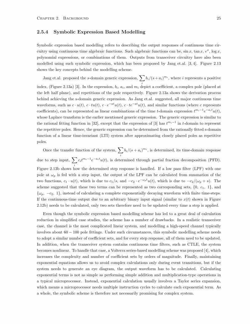
2.5.4 Symbolic Expression Based Modelling
Symbolic expression based modelling refers to describing the output responses of continuous time cir-
cuitry using continuous time algebraic functions. Such algebraic functions can be, sinx, tanx, ex, log x,
polynomial expressions, or combinations of them. Outputs from transceiver circuitry have also been
modelled using such symbolic expression, which has been proposed by Jang et.al. [3, 4]. Figure 2.13
shows the key concepts behind the modelling scheme.
Jang et.al. proposed the s-domain generic expression,∑i
bi/(s+ai)mi , where i represents a positive
index, (Figure 2.13a) [3]. In the expression, bi, ai, and mi depict a coefficient, a complex pole (placed at
the left half plane), and repetitions of the pole respectively. Figure 2.13a shows the derivation process
behind achieving the s-domain generic expression. As Jang et.al. suggested, all major continuous time
waveforms, such as c · u(t), c · tu(t), c · e−atu(t), c · te−atu(t), and similar functions (where c represents
coefficients), can be represented as linear combinations of the time t-domain expression tmi−1e−aitu(t),
whose Laplace transform is the earlier mentioned generic expression. The generic expression is similar to
the rational fitting function in [32], except that the expression of [3] has tmi−1 in t-domain to represent
the repetitive poles. Hence, the generic expression can be determined from the rationally fitted s-domain
function of a linear time-invariant (LTI) system after approximating closely placed poles as repetitive
poles.
Once the transfer function of the system,∑i
bi/(s+ ai)mi , is determined, its time-domain response
due to step input,∑i
citmi−1e−aitu(t), is determined through partial fraction decomposition (PFD).
Figure 2.13b shows how the determined step response is handled. If a low pass filter (LPF) with one
pole at ωp is fed with a step input, the output of the LPF can be calculated from summation of the
two functions, c1 · u(t), which is due to c1/s, and −c2 · e−ωptu(t), which is due to −c2/(ωp + s). The
scheme suggested that these two terms can be represented as two corresponding sets, 0, c1, 1, and
ωp, −c2, 1, instead of calculating a complete exponentially decaying waveform with finite time-steps.
If the continuous-time output due to an arbitrary binary input signal (similar to x(t) shown in Figure
2.12b) needs to be calculated, only two sets therefore need to be updated every time a step is applied.
Even though the symbolic expression based modelling scheme has led to a great deal of calculation
reduction in simplified case studies, the scheme has a number of drawbacks. In a realistic transceiver
case, the channel is the most complicated linear system, and modelling a high-speed channel typically
involves about 60− 100 pole fittings. Under such circumstances, this symbolic modelling scheme needs
to adopt a similar number of coefficient sets, and for every step response, all of them need to be updated.
In addition, when the transceiver system contains continuous time filters, such as CTLE, the system
becomes nonlinear. To handle that case, a Volterra series-based modelling scheme was proposed [4], which
increases the complexity and number of coefficient sets by orders of magnitude. Finally, maintaining
exponential equations allows us to avoid complex calculations only during event transitions, but if the
system needs to generate an eye diagram, the output waveform has to be calculated. Calculating
exponential terms is not as simple as performing simple addition and multiplication-type operations in
a typical microprocessor. Instead, exponential calculation usually involves a Taylor series expansion,
which means a microprocessor needs multiple instruction cycles to calculate each exponential term. As
a whole, the symbolic scheme is therefore not necessarily promising for complex system.
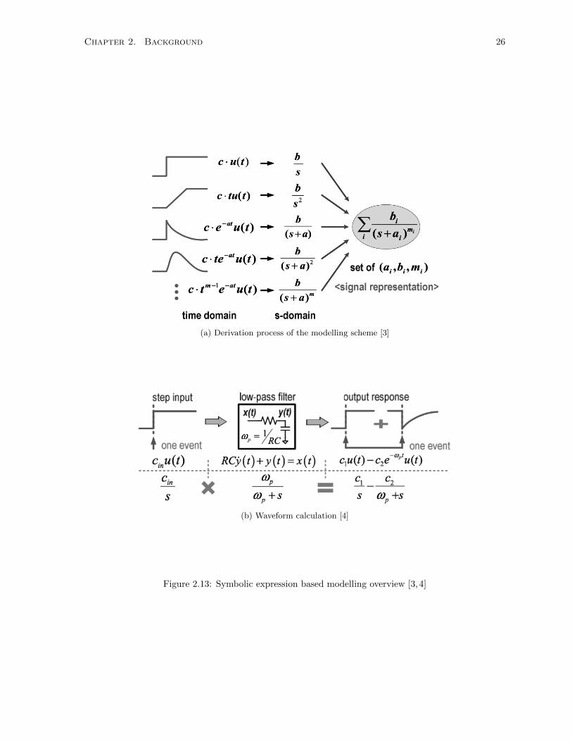
Chapter 2. Background 26
(a) Derivation process of the modelling scheme [3]
(b) Waveform calculation [4]
Figure 2.13: Symbolic expression based modelling overview [3,4]

Chapter 2. Background 27
2.6 Summary
This chapter has discussed the background necessary to proceed to the next chapters dealing with
equalizer and CDR modelling and their optimized validation procedures. Signal integrity in terms
of high-speed data transmission performance evaluations is covered from both signal attenuation and
timing uncertainty perspectives. Then, computational processing schemes applicable to transceiver
circuitry evaluation under long time simulation environments are covered. Throughout the discussion,
critical analysis creates the base for further potential developments on the topic of transceiver circuitry
modelling.
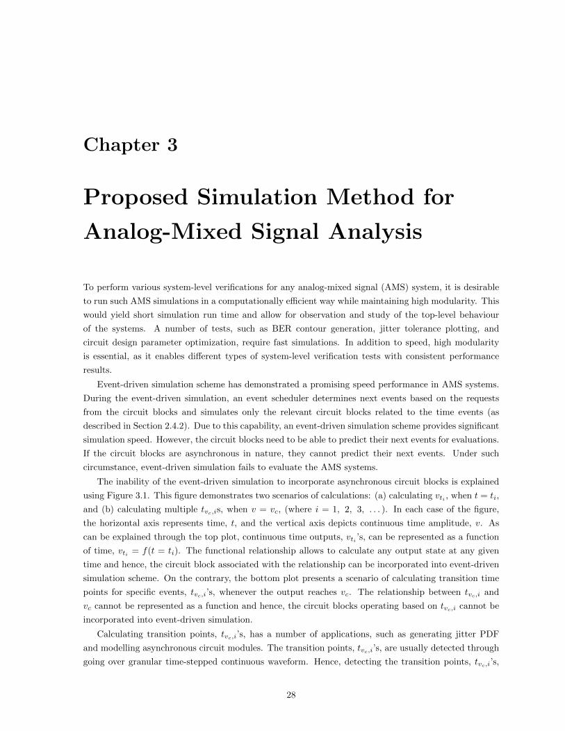
Chapter 3
Proposed Simulation Method for
Analog-Mixed Signal Analysis
To perform various system-level verifications for any analog-mixed signal (AMS) system, it is desirable
to run such AMS simulations in a computationally efficient way while maintaining high modularity. This
would yield short simulation run time and allow for observation and study of the top-level behaviour
of the systems. A number of tests, such as BER contour generation, jitter tolerance plotting, and
circuit design parameter optimization, require fast simulations. In addition to speed, high modularity
is essential, as it enables different types of system-level verification tests with consistent performance
results.
Event-driven simulation scheme has demonstrated a promising speed performance in AMS systems.
During the event-driven simulation, an event scheduler determines next events based on the requests
from the circuit blocks and simulates only the relevant circuit blocks related to the time events (as
described in Section 2.4.2). Due to this capability, an event-driven simulation scheme provides significant
simulation speed. However, the circuit blocks need to be able to predict their next events for evaluations.
If the circuit blocks are asynchronous in nature, they cannot predict their next events. Under such
circumstance, event-driven simulation fails to evaluate the AMS systems.
The inability of the event-driven simulation to incorporate asynchronous circuit blocks is explained
using Figure 3.1. This figure demonstrates two scenarios of calculations: (a) calculating vti , when t = ti,
and (b) calculating multiple tvc,is, when v = vc, (where i = 1, 2, 3, . . . ). In each case of the figure,
the horizontal axis represents time, t, and the vertical axis depicts continuous time amplitude, v. As
can be explained through the top plot, continuous time outputs, vti ’s, can be represented as a function
of time, vti = f(t = ti). The functional relationship allows to calculate any output state at any given
time and hence, the circuit block associated with the relationship can be incorporated into event-driven
simulation scheme. On the contrary, the bottom plot presents a scenario of calculating transition time
points for specific events, tvc,i’s, whenever the output reaches vc. The relationship between tvc,i and
vc cannot be represented as a function and hence, the circuit blocks operating based on tvc,i cannot be
incorporated into event-driven simulation.
Calculating transition points, tvc,i’s, has a number of applications, such as generating jitter PDF
and modelling asynchronous circuit modules. The transition points, tvc,i’s, are usually detected through
going over granular time-stepped continuous waveform. Hence, detecting the transition points, tvc,i’s,
28

Chapter 3. Proposed Simulation Method for Analog-Mixed Signal Analysis 29
t1 t2 t3 · · ·
vt1vt2
vt3
i = 1, 2, 3, . . .
(a) Calculating vti , when t = ti
v = vc
tvc,1 tvc,2 tvc,3 · · ·i = 1, 2, 3, . . .
(b) Calculating tvc,is, when v = vc
Figure 3.1: Comparative study between calculating vti and tvc,i
is currently available only in time-step based simulation scheme. In time-step based simulation, the
simulator needs to repetitively select different time-points around each tvc,i, until the simulator reaches
to that tvc,i within specified error bound (as explained in Section 2.4.1). However, the process of
detecting transition points, tvc,i’s, is usually time consuming and computationally inefficient, which is
further discussed in detail later in Section 3.3.1.
This chapter presents a new way of running AMS simulation system addressing the aforementioned
issue of calculating transition points, tvc,i’s. The new AMS simulation scheme is realizable in standard
object-oriented (OO) programming environment due to added benefits of high computation efficiency
and modularity. The rest of this chapter deals with how the proposed simulation method can be utilized
to achieve the desired benefits. Section 3.1 discusses the concept behind introducing OO simulation for
AMS system analyses. Next, Section 3.2 mentions about the key considerations for modelling such AMS
system and how the interactions occur among different varieties of circuit systems. Finally, Section 3.3
explains the detail process of operating the proposed simulation scheme and examines its performance
under various circumstances.
3.1 Object-Oriented (OO) Modelling Based Simulation
The concept of OO programming originated from the notion of imitating real-life object-to-object inter-
action [33]. In OO programming, each object can be designed to have its own properties and methods.
Properties of an object are internal fields or variables which are to store the state information of the
object for time-to-time usage without direct external intervention. Similarly, methods of an object are
internal functions, which are applied to describe object-specific algorithms or routines to perform various

Chapter 3. Proposed Simulation Method for Analog-Mixed Signal Analysis 30
activities, such as output calculation, object-to-object interaction, and output visualization. Another
noteworthy features of OO programming is that objects of new classes can be derived from other similar
or parent classes to describe their behaviour with minimal effort. These types of attributes make the
OO programming an attractive choice for modelling wide varieties of systems like AMS circuitry.
3.1.1 Abstraction for OO Simulation
Any AMS system like transceiver circuitry can be easily represented in OO programming based simula-
tion (in short OO simulation) scheme. All circuit components in an AMS system can be classified either
as discrete time or continuous time components. Output states generated by discrete time components
change only during their corresponding discrete time events, whereas outputs from continuous time cir-
cuit components vary always with respect to their input variation in time. During the proposed OO
simulation, all components regardless of their types are treated independently to calculate their outputs
using their own algorithms. Outputs are calculated based on the input information which are received
through object-to-object interactions. This allows to have individual time-steps and evaluation process
for different circuit components and it is particularly beneficial for continuous time components, which
are not directly related to each other, due to facilitating de-unionized time point selection unlike the
case of time-step based simulators.
Figure 3.2 explains how the OO simulator can be abstracted for an AMS system. Three discrete time
components, D1, D2, and D3, and two continuous time components, C1 and C2 are shown in Figure
3.2a as representative components of an AMS system. D1 and D2 work as two independent sources for
the representative AMS system, while C1 receives input from the discrete time source D1 and feeds its
output to the discrete time component D3. D3 receives inputs from C1 and D2. Lastly, C2 receives
input from D2 and D3.
The AMS system presented in Figure 3.2a can be translated for OO simulation purpose like the way
shown in Figure 3.2b. In Figure 3.2b, there are two types of blocks: circuit objects and a host platform.
Circuit components D1, D2, D3, C1, and C2 are represented as circuit objects objD1, objD2, objD3,
objC1, and objC2 respectively. Depending on the operation type of circuit objects, they can be of the
same class or different classes. All circuit objects maintain similar input-output relationship just like the
representative AMS system during the OO simulations. The solid arrow points to the direction, where
the processed outputs of circuit objects are flowing. Task of the host platform is to ensure the process
output flow between circuit objects, until the simulation is completed. Here, interaction between host
and each circuit object is shown using a dotted arrow.
3.1.2 Operating Principle of OO Simulation
In the proposed OO simulation scheme, the simulation is conducted primarily through establishing
interactions among circuit objects. All circuit objects are designed to handle their individual simulation
processes. Hence, the proposed OO simulation scheme at the top-level only needs to coordinate with
the circuit objects, until individual processing time of each circuit object arrives to the user-defined stop
time.
During the simulation, all the circuit objects are activated to process their inputs based on the
received input information from their preceding objects by the top-level simulation coordinator (or the
host platform). As indicated in the Algorithm 3.1, the OO simulation involves two phases: initialization
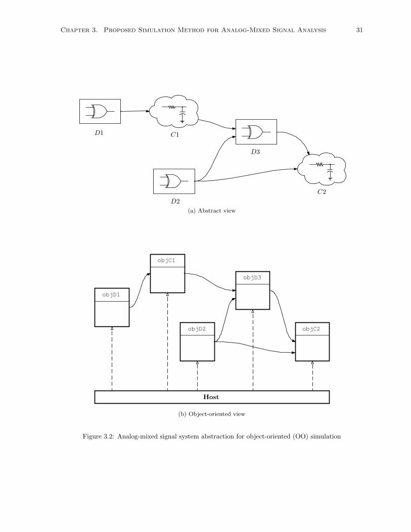
Chapter 3. Proposed Simulation Method for Analog-Mixed Signal Analysis 31
D1
D2
D3
C1
C2
(a) Abstract view
objD1
objD2
objD3
objC1
objC2
Host
(b) Object-oriented view
Figure 3.2: Analog-mixed signal system abstraction for object-oriented (OO) simulation
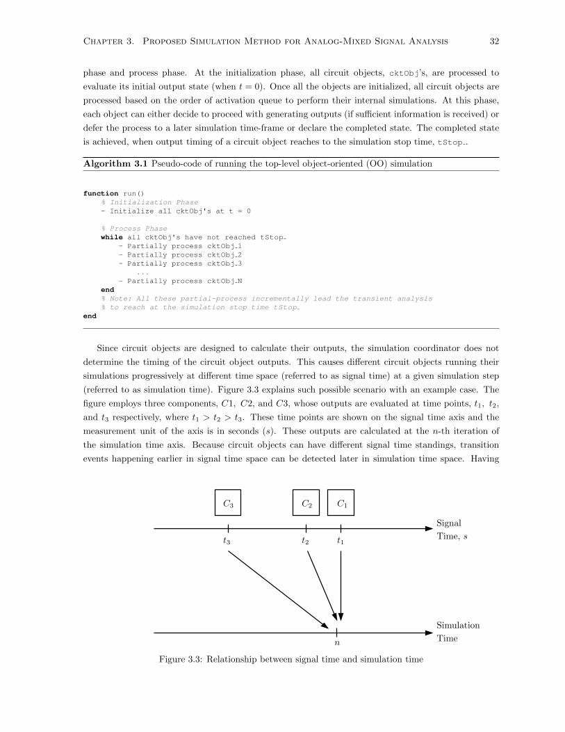
Chapter 3. Proposed Simulation Method for Analog-Mixed Signal Analysis 32
phase and process phase. At the initialization phase, all circuit objects, cktObj’s, are processed to
evaluate its initial output state (when t = 0). Once all the objects are initialized, all circuit objects are
processed based on the order of activation queue to perform their internal simulations. At this phase,
each object can either decide to proceed with generating outputs (if sufficient information is received) or
defer the process to a later simulation time-frame or declare the completed state. The completed state
is achieved, when output timing of a circuit object reaches to the simulation stop time, tStop .
Algorithm 3.1 Pseudo-code of running the top-level object-oriented (OO) simulation
function run()% Initialization Phase- Initialize all cktObj's at t = 0
% Process Phasewhile all cktObj's have not reached tStop
- Partially process cktObj 1- Partially process cktObj 2- Partially process cktObj 3
...- Partially process cktObj N
end% Note: All these partial-process incrementally lead the transient analysis% to reach at the simulation stop time tStop
end
Since circuit objects are designed to calculate their outputs, the simulation coordinator does not
determine the timing of the circuit object outputs. This causes different circuit objects running their
simulations progressively at different time space (referred to as signal time) at a given simulation step
(referred to as simulation time). Figure 3.3 explains such possible scenario with an example case. The
figure employs three components, C1, C2, and C3, whose outputs are evaluated at time points, t1, t2,
and t3 respectively, where t1 > t2 > t3. These time points are shown on the signal time axis and the
measurement unit of the axis is in seconds (s). These outputs are calculated at the n-th iteration of
the simulation time axis. Because circuit objects can have different signal time standings, transition
events happening earlier in signal time space can be detected later in simulation time space. Having
C1C2C3
t1t2t3
Signal
Time, s
n
Simulation
Time
Figure 3.3: Relationship between signal time and simulation time

Chapter 3. Proposed Simulation Method for Analog-Mixed Signal Analysis 33
this splitting flexibility of the signal time axis for circuit objects allows the OO simulation scheme to
incorporate the asynchronous circuit objects, while having the similar circuit spatiotemporal optimization
of event-driven simulation.
Due to activating circuit objects not in the ascending order of their time events, circuit objects can
be enlisted in the activation queue of simulation coordinator in any order. The random ordering in
activation queue only cause activation of circuit objects at immature state, but circuit objects have
the options to defer their processes. Also, this phenomenon of wrong activation only happens in the
initial simulation time-frame, but diminishes gradually, as the simulation progresses. In reality, the total
number of wrong activation solely depends on the enlisting order of the circuit objects and is independent
of the actual simulation stop time (see Section 3.3.2 for proof). Hence, the OO simulation performance
does not suffer from the random order of circuit objects in the activation queue.
3.2 Description of Circuit Objects
Dealing with circuit objects for simulation purposes is like managing supply chain for manufacturing
process. Each circuit object of Figure 3.2b can be visualized as a unit for processing received information
packet and then sending the processed output packet to its destination. In order to function as an
independent simulation unit, each circuit object needs to have its own internal properties and individual
methods for generating outputs.
cktObj
Properties
MethodsReceivingInputs
SendingOutputs
Input Objectsfor cktOj
Output Objectsfor cktOj
Figure 3.4: Definition of a circuit object, cktObj
Figure 3.4 depicts the definition of such a circuit object unit with the capability to run independent
simulation process. In the figure, the block marked as cktObj defines the circuit object of interest.
Any circuit object like cktObj can have multiple input sources and multiple output sinks, which are
also similar circuit objects like cktObj. Each circuit object has a number of specialized properties and
methods, which are described in Section 3.2.1. The 3D cubic boxes represent the data information
generated by circuit objects, which are described in Section 3.2.2.
3.2.1 Properties and Methods of Circuit Objects
In order to utilize the modularity of OO programming, properties and methods of circuit objects are
required to be designed in a standardized format. Standardization in function (listed under methods)
design and variable (listed under properties) naming allows to establish common interface for object-
to-object interaction as well as to develop new circuit objects through inheritance. Common interface

Chapter 3. Proposed Simulation Method for Analog-Mixed Signal Analysis 34
becomes essential, when it comes to simulating a wide variety of circuit system combinations. Inheritance
brings user-friendly attributes for modelling systems through adopting properties and methods of the
other close circuit objects for the new circuit objects.
Algorithm 3.2 presents a pseudo-code for any circuit object, cktObj. The circuit object, cktObj,
is here inherited from a parent circuit object, paretObj in order to obtain all properties and methods
without repetitive declaration inside cktObj code block. If the cktObj has no parent, its inheritance is
declared as handle – it is basically a class to create new objects in dynamic memory space and to allow
access to that exact object during assignment operation (details can be found in [34]). The pseudo-
code block has two main segment: properties and methods. The properties are used for storing various
types of information, such as intermediate processed states, received inputs, generated outputs, and
object characteristics. The methods are used for describing activities at various stages, such as object
construction stage, initialization stage, input-receiving (and output-sending) stage, and processing stage.
Due to inheritance of OO programming, certain methods can be overloaded in the situation, which is
useful in designing new circuit objects. Inside the pseudo-code, some properties and mehtods are shown
under their respective sections.
Algorithm 3.2 Pseudo-code for a circuit object, cktObj
% Pseudo-code for cktObj (inherited from parentObj)classdef cktObj < parentObj
properties% Internal properties are described here
objTypinPortlastOut <Time>lastOut <State>lastIn <Time>lastIn <State>evtHost... other properties (not mentioned here)
end
methods% Simulation related functions are described here
function cktObj(input arguments) % Constructorfunction init() % Initializerfunction receive() % Input receiverfunction isComplete() % Answerer for completenessfunction process() % Output calculator... other methods (not mentioned here)
end
end
Table 3.1 describes about key considerations of major properties.

Chapter 3. Proposed Simulation Method for Analog-Mixed Signal Analysis 35
Table 3.1: Major properties of circuit objects
Name Description
objTyp 1 It is used to describe the type of circuit objects for a number of object-
to-object interaction purposes. For example, discrete type circuit objects
generate discrete time outputs, where continuous type circuit objects
generate continuous time outputs. Other circuit objects like simulation
measurement scopes generate no output. Certain circuit objects, with
different types of output such as symbolic type, can be introduced to the
simulation scheme simply by appending as a new type of circuit object.
Using the type allows to perform compatibility check or modified actions
at the output receiving end. This property is kept as constant throughout
lifespan of the object.
% For discrete type
objTyp = ObjTyp.discrete
% For continuous type
objTyp = ObjTyp.continuous
% For measurement scope type
objTyp = ObjTyp.scope
inPort It is used to store the input information related to input circuit object
(like handle to input circuit object). Object information of input circuitry
is required for various interaction purposes, such as collecting processed
output packets, requesting to hold on to a stage (for certain object),
navigating to the other circuit objects in the system chain. This property
is defined during the circuit object initialization and once defined, it is
kept constant throughout lifespan of the object.
lastOut <Time>
and
lastOut <State>
These properties work as temporary storage for recently processed output
package. The lastOut <Time> is used for storing timing information
and the lastOut <State> is for calculated output state information.
Their length must be same at all conditions. After every process phase,
old processed outputs are replaced by the newly processed outputs and
hence they are temporary storage. Because of that, the processed outputs
need to be saved immediately after each phase at the receiving ends.
% Storage format for processed information
last <Time> = [t1, t2, t3, , tN]; % Size: N x 1
last <State> = [s1, s2, s3, , sN]; % Size: N x 1
1Properties end with a underscore ( ) at the end

Chapter 3. Proposed Simulation Method for Analog-Mixed Signal Analysis 36
Continuation of Table 3.1
Name Description
lastIn <Time>
and
lastIn <State>
These two properties work as storage for unprocessed information pack-
age received from input circuit objects. The lastIn <Time> is used
to store timing information and the lastIn <State> is for received in-
put state information. They are strictly of same size like the case of
lastOut <Time> and lastOut <State>. Whenever new input infor-
mation being received, they are appended to old input information and
after each processing phase, unwanted information are trimmed off. The
appending and trimming actions help to reduce the demand for computa-
tional memory and results in constant computational speed throughout
the simulation period. These properties are kept as protected to prevent
from potential external corruption.
% Storage format for appended received information
lastIn <Time> = [lastIn <Time>, inPort .lastOut <Time> ];
lastIn <State> = [lastIn <State>, inPort .lastOut <State>];
% |------Old------|----------New-----------|
evtHost It is used to store the object information of top-level simulation coordi-
nator. The coordinator can be considered as a host for requesting events
from circuit objects – in short, event host. Besides coordinating, it con-
tains a number of global information, such as simulation stop time and
order of pulse amplitude modulation (PAM).
% All sharable properties can be defined like this.
% For example,
evtHost .tStop % Simulation stop time
evtHost .pamOrder % Simulation PAM order
% ...
End of Table
Table 3.1 presents only the common and standard properties within the circuit objects. Besides these
properties, each circuit object can have specific properties. For instance, the circuit object PRBS has a
property called order , which represents the number of flip-flops in a PRBS, such as 3, 7, 15, and 31.
Within the circuit object, all properties can have their setter and getter methods to control their be-
haviour, such as specifying acceptable inputs, future changeability, and access restriction. This type of
controlling features or encapsulation helps to prevent unwanted circuit behaviours during simulation.
We now present the list of major methods for modelling circuit objects in Table 3.2.

Chapter 3. Proposed Simulation Method for Analog-Mixed Signal Analysis 37
Table 3.2: Major methods of circuit objects
Name Description
Constructor This method is responsible for not only creating the object itself but also
performing its first-stage initialization. It takes the name of the circuit
object it is defined for. All essential properties, like inPort and object
specific parameters, are defined at this phase. It is invoked when the ob-
ject is declared in the top-level script. Pseudo-code for the constructor
is described below.
classdef cktObj < handle
methods
function cktObj(input arguments) % Constructor
- Define input ports
- Initialize object specific parameters
end
end
end
init()2 This method is called at the initialization phase performed by the simu-
lation coordinator. This phase is the second-stage initialization and the
stage is added to reduce the top-level scripting and thereby to facilitate
user-friendly coding styles. At this phase, all remaining internal proper-
ties are defined so that the circuit object is prepared to enter into the
processing phase. Certain internal properties often have dependency on
the initial output states of the inPort . Hence, the method needs to be
invoked, once the method init() of the inPort is completed. If the
circuit object has multiple input sources, the init() of the circuit object
can be called either once or multiple times by the similar methods of the
chosen input sources. Pseudo-code for the init() is described below.
function init() % Initializer
- Initialize any remaining undefined property
- Calculate initial output (at t = 0)
end
2Methods end with brackets at the end.

Chapter 3. Proposed Simulation Method for Analog-Mixed Signal Analysis 38
Continuation of Table 3.2
Name Description
receive() This method is used for receiving processed information from the inPort
object. Every time the inPort has completed its processing, the method
is invoked to append the processed information to the previously received
information at the properties lastIn <Time> and lastIn <State>.
Hence, calling the receive() repeatedly causes the sizes of the properties
to get bigger indefinitely, which may bring undesirable effects of higher
memory resource and lower computational speed, (unless the vectors are
trimmed off through processing at the same growth rate). Pseudo-code
for the receive() is described below.
function receive() % Input receiver
- Append to the previously stored input information
end
isComplete() This method is used for providing feedback to the system coordinator
about the simulation status of the circuit object. It provides logical out-
put true, if the signal time of the circuit object exceeds the simulation
stop time, tStop ; otherwise, it raises the flag as false to indicate the
incomplete status of processing. Pseudo-code for the isComplete() is
described below.
function isComplete() % Completeness answerer
return maxlast <Time> ≥ evtHost .tStop
end
One noteworthy fact about the completion status would be mostly false
since the initial stage. Once the processing is completed, the status would
be true onward. The behaviour is more like a unit step function, which is
implementation friendly for branch prediction based computation scheme.

Chapter 3. Proposed Simulation Method for Analog-Mixed Signal Analysis 39
Continuation of Table 3.2
Name Description
process() Core functionality of the OO simulation is performed by this method.
It is invoked by the simulation coordinator either directly or through
helper circuit objects (with state holding capability). Holding on to a
state becomes necessary when the simulation process for the object can-
not be performed due to the lack of available input information. The
helper circuit object with holding state capability is developed in order
to reduce repetitive coding. Algorithm related to the circuit object is
described inside the method process(). Once the method is completed,
the processed information is saved in the fields lastOut <Time> and
lastOut <State>. Pseudo-code for the method process() is described
below.
function process() % Output calculator
- Identify next time event
if not enough input information received
- Hold on to the state
return
end
- Process input information
- Save the processed information
- Discard unnecessary input information
- Notify about process completion
end
As can be seen, the method process() trims off unnecessary input infor-
mation from the properties lastIn <Time> and lastIn <State>. This
allows to keep their sizes within manageable limits to avoid potential sim-
ulation slow speed issues (which is highlighted earlier). Once the method
process() is completed, it can either return back to the main routine
run() or initiate process()’s of other circuit objects.
End of Table
Like the case of property analysis, Table 3.2 only includes major methods for any circuit object.
These major methods are relevant to simulation interactions. As can be observed from the table, the
Constructor and init() are both called once for initialization purposes during the simulation. Because
of that, their contributions to the simulation run time is mostly negligible and hence their efficiency in
simulation speed is irrelevant. Other three methods, receive(), isComplete(), and process(), are
called numerous times. The simulation length, set by the tStop , defines how many times these methods
are called. Hence, simulation speed performance is directly affected by the efficiencies of these three
methods, because the task of the top-level simulation coordinator (which is function run(), as described
by Algorithm 3.1) has been significantly simplified. Among the three methods, the process() is the
most computationally intensive and the overall elapsed time is mostly dominated by the process()’s of

Chapter 3. Proposed Simulation Method for Analog-Mixed Signal Analysis 40
all circuit objects.
Besides these major methods, a number of other methods can be defined for various purposes. For
instance, if the output of a circuit object is enabled to save, the output can be displayed in a graphical
window using the method plot(). In this case, the plot(), specifically defined for the circuit object,
has been overloaded with other built-in plot() functions.
3.2.2 Processed Data Formats of Circuit Objects
One of the major concerns in circuit simulations is the co-simulation of the continuous time circuit
components with discrete time circuit components in event-driven mode. This section discusses the
format of the processed data, which can be used to establish the interactions among such circuit objects
(shown as 3D cubic box in Figure 3.4). Figure 3.5 presents an equivalent relationship between discrete
time and continuous time circuit objects for OO simulation purposes. Details about each processed data
format are presented in the following.
Discrete Time Objects
As explained in Section 2.4, output of a discrete time component comprises of discrete output states
at their corresponding discrete time events. Accordingly, the top part of Figure 3.5 presents how the
output of a discrete time components can be presented as two equally sized sequences: a time sequence,
TD = (ti)Ni=0, where t0 = 0, and a state sequence, SD = (si)
Ni=0. At each time event, ti, the discrete
time component generates a discrete state, si, and its initial state, s0, is defined at the time event, t0.
In the proposed OO simulation scheme, the state sequence, SD, is designed such that consecutive states
are usually not allowed to be equal, si 6= si−1, where i = 1, 2, . . . N . This is to minimize unnecessary
object-to-object interactions and achieve the speed advantages of event-driven simulation.
For Discrete Time Objects
Time, TD =(
0, t1, t2, . . . ti, . . . tN
)State, SD =
(s0, s1, s2, . . . si, . . . sN
)
For Continuous Time Objects
Time, TC =(
0,(tk,1)K1
k=1,
(tk,2)K2
k=1, . . .
(tk,i)Ki
k=1, . . .
(tk,N
)KN
k=1
)Waveform, WC =
(w0,
(wk,1
)K1
k=1,(wk,2
)K2
k=1, . . .
(wk,i
)Ki
k=1︸ ︷︷ ︸, . . .(wk,N
)KN
k=1
)i-th Wavelet, wi
here,(tk,i)Ki
k=1,= (t1,i, t2,i, . . . tKi,i), tk,i ∈ (ti−1, ti], tk,i = tk−1,i + ∆tk,i︸ ︷︷ ︸
Time Step
Figure 3.5: Processed data format comparison for the cases of discrete time and continuous time objects

Chapter 3. Proposed Simulation Method for Analog-Mixed Signal Analysis 41
Regarding the time sequence, TD, all consecutive time events, ti’s, are generated in such a way
that they can be progressively increasing, 0 < t1 < t2 < · · · < tN , during the simulation. This is in
contrast with the situation in conventional time-step based simulation, where if the operation of any
discrete time component depends on the transition points of a continuous time component as an input
source, the simulator often has to move back and forth along the time axis to find the transition points,
which causes certain calculations to be performed repetitively (see [1] for details). In the proposed
scheme, progressively increasing order of the time sequence elements, (ti − ti−1)Ni=1 > 0, is maintainable
throughout the simulation, because circuit objects can be at different signal time simultaneously at any
given simulation time.
Continuous Time Objects
For continuous time components, the continuous output waveform needs to be represented with multiple
discrete time outputs spaced at reasonable time-steps. Continuous-like discrete time output has a number
of applications in transceiver simulations, such as eye diagram generations, jitter measurements, and
asynchronous circuit block simulations. In order to support such continuous-like outputs in event-driven
simulation mode, a continuous time waveform, WC , recorded for an interval, [0, tN ], can be visualized
as multiple wavelets, which are recorded for smaller intervals, 0, (0, t1], (t1, t2], . . . (tN−1, tN ]. Figure
3.5 shows how such continuous time wavelets with relevant intervals can be aligned with their respective
discrete time outputs. Like the case of discrete time objects, the initial output, w0, for continuous time
objects recoded at t = 0, is a scalar. For the rest of the cases, any wavelet, wi, which itself is considered
as a sub-sequence, (wk,i)Ki
k=1, recorded at corresponding time sub-sequence, (tk,i)Ki
k=1, is comparable to
the respective discrete output event, si, at ti. Discrete time points for any i-th wavelet, tk,i’s, are selected
from the respective interval, (ti−1, ti]. Inside the time sub-sequence, each element, tk,i, is incremented
from the previous element, tk−1,i, by its respective time step, ∆tk,i.
Depending on the simulation requirements, time steps can be picked as constant or variable. A
constant time step can be useful for generating an eye diagram, because the generation process involves
sampling at a fixed time step. Time step, ∆ti, can be kept constant within a time sub-sequence, but
might need to be varied over entire simulation period, because all time intervals, (ti−1, ti]’s, might not
be the perfect multiples of the initially chosen time step. A variable time step can be useful for detecting
transition points like determining zero-crossings to improve simulation speed. Regardless, all time points
in (tk,i)Ki
k=1 must be selected within the given interval, (ti−1, ti], to avoid non-causality effects. This
segmentation process enables running continuous time components in event-driven mode.
3.3 Performance Evaluation of OO Simulation in Case Studies
We evaluate the performance of OO simulation through examples in this section. Section 3.3.1 is used
to study the simulation steps in detail for a simple example case. This example case is analyzed in
terms of the order of processing circuit objects for various combinations in Section 3.3.2. Later, Section
3.3.4 explains how the proposed OO simulation can be implemented for parallel processing environment.
Section 3.3.3 discusses the simulation situations, if the system has feedback.

Chapter 3. Proposed Simulation Method for Analog-Mixed Signal Analysis 42
ClockPRBS
Random Bit-stream Generator
Transmitter
Channel
Receiver
Slicer
VClk VRBG VCh VRx
(a) Block-level schematic
VClk
VRBG
VCh
VRx
-
Signal Time, t
Simulation Time: 1, 2, 3, . . .
t1 t2 t3 t4 t5
t1a t2a t3a t4a t5a
1 2 3 4 5
2 3 4 5 6
3 4 5 6 7
(b) Output waveforms with added markings
Figure 3.6: Simulation test case study for OO simulation

Chapter 3. Proposed Simulation Method for Analog-Mixed Signal Analysis 43
3.3.1 Example Case Study
Figure 3.6 shows the block-level testbench of a simple transceiver circuit used for the evaluation and its
corresponding output waveforms generated from the simulation with added markings for future reference.
The transceiver employs three major blocks: a random bit-stream generator (RBG) (at the trasmitter
side), a data transmission channel, and a slicer (at the receiver side). The RBG consists of a PRBS
generator fed by a clock producing a synchronous binary output. In the waveform plot, the horizontal
axes for all cases represent time, t. The second plot from the top shows a sample output waveform from
the RBG, VRBG, which is generated at the clock transitions (both rising and falling), VClk. The third
plot depicts the output waveform of the channel, VCh, calculated at a sample rate much higher than the
clock frequency to demonstrate its continuous nature. The task of the slicer is to produce a binary data
corresponding to its continuous input. The fourth plot shows the binary output of the slicer, VRx.
During the OO simulation, all major blocks are modelled as independent objects. Table 3.3 presents
object-specific properties, which are required during the object construction.
Table 3.3: Description of object-specific properties for the selected object-oriented simulation case
Object Property Value
RBG objTyp It is defined as ObjTyp.discrete by default, since the rep-
resentative component is of discrete type.
inPort It is kept empty, [], since the component has no input source.
clkPeriod It defines the period for the internal clock. Since the PRBS
flip-flops are configured for both edge operation, it is set to be
twice of an UI.
prbsState It defines the output binary states of the PRBS flip-flops. It is
actually a vector and its length is determined by the number
of the flip-flops. Elements in the vector are updated at every
clock phase based on the PRBS polynomial expression.
Channel objTyp It is defined as ObjTyp.continuous , because slicer operation
requires continuous time wavelets.
inPort It contains the handle information related to the object RBG.
modelInfo It is utilized to describe the channel model. Its content depends
on how the channel is modelled for simulation. For instance,
it contain step response amplitude and timing information, if
the object is modelled based on step responses.
Chapter 3. Proposed Simulation Method for Analog-Mixed Signal Analysis 44
Continuation of Table 3.3
Object Property Value
Slicer objTyp It is defined as ObjTyp.discrete , because slicer outputs only
contains transition event of the channel.
inPort It contains the handle information of the object channel.
threshold It defines the assigned threshold to make the binary decision.
Here, its value is set at the mid-point of the VClk amplitude
range.
End of Table
The above table also does not discuss about certain properties, such as evtHost , lastIn <Time>,
and lastIn <State>. These properties are discussed earlier in Table 3.1. Simulation-specific methods
(except isComplete()) for all objects are presented as follows.
Table 3.4: Simulation-specific properties of all objects for the selected object-oriented simulation case
Object Method Routine
RBG init() This method defines the properties lastOut <Time> and
lastOut <State> to represent its initial output.
receive() Since the object does not have any input source, this method
does not exist.
process() This method is responsible to generate the output. It is respon-
sible to calculate the PRBS output with respect to the clock
transitions. Its routine can be described as follows.
function process()
while no PRBS transition is detected
- Use clkPeriod to define the next clock ...
transition
- Perform the PRBS operation
- Update the prbsState
end
- Update lastOut <Time> and lastOut <State>
- Notify the Channel to receive its output
end

Chapter 3. Proposed Simulation Method for Analog-Mixed Signal Analysis 45
Continuation of Table 3.4
Object Method Routine
Channel init() It calculates the initial output at t = 0 based on the initial
state of the RBG.
receive() This method receives the processed output from the RBG ob-
ject and appends them to the properties lastIn <Time> and
lastIn <State>.
process() Its task is to calculate the continuous time output.
function process()
if no input information is available
- hold on to the state
return
end
- Calculate its continuous time output
- Store the output at lastOut <Time> and ...
lastOut <State>
- Notify the Slicer to receive its output
end
Slicer init() It defines the initial state of the slicer based on the initial
output of the channel.
receive() This method receives continuous time output from the channel
and then identifies the slicing location on the continuous time
waveform.
function receive()
- Receive continuous time output from channel
% Pre-process
- Detects the threshold-crossing locations, t i's
- Assigns output states for all t i's
- Append t i's and its states to lastOut <Time> ...
and lastOut <State>
end
Chapter 3. Proposed Simulation Method for Analog-Mixed Signal Analysis 46
Continuation of Table 3.4
Object Method Routine
process() Task of this method is to generate time events based on the
detected crossing locations.
function process()
if lastOut <Time> is empty
return
end
- Generate an time event using the first crossing
- Remove the first crossing
end
End of Table
As can be seen, the receive()’s for all objects perform the task of receiving input (if input source is
available), except for the slicer, in which case, the method also performs some pre-processing to simplify
the task of the slicer process(). It is intuitive for the slicer to save only the detected threshold-crossings
instead of entire continuous time waveform from the channel, since it reduces the memory requirement
for slicer operation.
Table 3.5 explains step-by-step how the simulation is conducted in OO mode. As mentioned in
Section 3.1.2, the enlisted object order does not matter for running OO simulation. Therefore, let us
assume the objects are enlisted in the following order: a. slicer, b. channel, and c. RBG. Based on the
Algorithm 3.1, the simulation steps are described as follows:
Table 3.5: Explanation of simulation steps for the selected object-oriented simulation case (for simulationtime 0 - 4)
Simulation Time Action
03 At the initial step, all circuit objects are initialized. Since the RBG has
no input source, its method init() perform the initialization indepen-
dently at first. Next, the channel method init() is initialized based on
the initial state of the RBG. Later, the slicer performs its initialization
similarly based on the initial output at t = 0 of the channel.
3represents the initialization phase

Chapter 3. Proposed Simulation Method for Analog-Mixed Signal Analysis 47
Continuation of Table 3.5
Simulation Time Action
1 This step progresses as follows.
a Slicer: Since no input is available for processing, its process()
declares a hold state.
b Channel: Since no input is available for processing, its process()
declares a hold state.
c RBG: Its process() generates the first output at time event, t1.
2 This step proceeds as follows.
a Slicer: Since no input is available for processing, its process()
still remains at the hold state.
b Channel: Its process() produces continuous time output se-
quence for (tk,1)K1
k=1, where tk,1 ∈ (0, t1].
c RBG: Its process() generates the output at time event, t2.
3 This step proceeds as follows.
a Slicer: Its process() goes over the received waveform recorded
at (tk,1)K1
k=1, but detects no transition at the defined threshold, and
hence no output is generated.
b Channel: Its process() produces continuous time output se-
quence for (tk,2)K2
k=1, where tk,2 ∈ (t1, t2].
c RBG: Its process() generates the output at time event, t3.
4 This step proceeds as follows.
a Slicer: Its process() detects the first transition event at t1a.
b Channel: Its process() produces continuous time output se-
quence for (tk,3)K3
k=1, where tk,3 ∈ (t2, t3].
c RBG: Its process() generates the first output at time event, t4.
End of Table
As can be observed at simulation time 4 that all circuit objects are processing their received input
information and generating outputs. This pattern of processing for all circuit objects will repeat at
all future simulation time, 5, 6, 7, . . . , until the process() methods of all the circuit objects stop
processing. When a circuit object has reached its processing to the end of the signal time, it stops
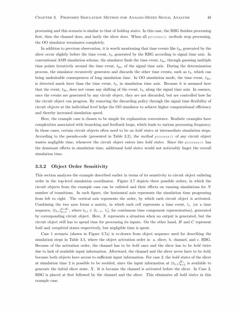
Chapter 3. Proposed Simulation Method for Analog-Mixed Signal Analysis 48
processing and this scenario is similar to that of holding states. In this case, the RBG finishes processing
first, then the channel does, and lastly the slicer does. When all process() methods stop processing,
the OO simulator terminates completely.
In addition to previous observation, it is worth mentioning that time events like t2a generated by the
slicer occur slightly before the time event, t3, generated by the RBG according to signal time axis. In
conventional AMS simulation scheme, the simulator finds the time event, t2a, through guessing multiple
time points iteratively around the time event, t2a, of the signal time axis. During the determination
process, the simulator recursively generates and discards the other time events, such as t3, which can
bring undesirable consequences of long simulation time. In OO simulation mode, the time event, t2a,
is detected much later than the time event, t3, in simulation time axis. Because it is assumed here
that the event, t2a, does not cause any shifting of the event, t3, along the signal time axis. In essence,
once the events are generated by any circuit object, they are not discarded, but are controlled how far
the circuit object can progress. By removing the discarding policy through the signal time flexibility of
circuit objects at the individual level helps the OO simulator to achieve higher computational efficiency
and thereby increased simulation speed.
Here, the example case is chosen to be simple for explanation convenience. Realistic examples have
complexities associated with branching and feedback loops, which leads to various processing frequency.
In those cases, certain circuit objects often need to be on hold states at intermediate simulation steps.
According to the pseudo-code (presented in Table 3.2), the method process() of any circuit object
wastes negligible time, whenever the circuit object enters into hold states. Since the process() has
the dominant effects in simulation time, additional hold states would not noticeably linger the overall
simulation time.
3.3.2 Object Order Sensitivity
This section analyzes the example described earlier in terms of its sensitivity to circuit object enlisting
order in the top-level simulation coordinator. Figure 3.7 depicts three possible orders, in which the
circuit objects from the example case can be enlisted and their effects on running simulations for N
number of transitions. In each figure, the horizontal axis represents the simulation time progressing
from left to right. The vertical axis represents the order, by which each circuit object is activated.
Combining the two axes forms a matrix, in which each cell represents a time event, ti, (or a time
sequence, (tk,i)k=Ki
k=1 , where tk,i ∈ (ti−1, ti], for continuous time component representation), generated
by corresponding circuit object. Here, X represents a situation when no output is generated, but the
circuit object still has to spend time for processing its inputs. On the other hand, H and C represent
hold and completed states respectively, but negligible time is spent.
Case 1 scenario (shown in Figure 3.7a) is re-drawn from object sequence used for describing the
simulation steps in Table 3.5, where the object activation order is: a. slicer, b. channel, and c. RBG.
Because of the activation order, the channel has to be held once and the slicer has to be held twice
due to lack of available input information. Afterward, the channel and the slicer never have to be held,
because both objects have access to sufficient input information. For case 2, the hold states of the slicer
at simulation time 2 is possible to be avoided, since the input information at (tk,1)K1
k=1 is available to
generate the initial slicer state, X. It is because the channel is activated before the slicer. In Case 3,
RBG is placed at first followed by the channel and the slicer. This eliminates all hold states in this
example case.

Chapter 3. Proposed Simulation Method for Analog-Mixed Signal Analysis 49
a.S
lice
rH
HX
t 1a
···
t (N−3)a
t (N−2)a
t (N−1)a
b.
Ch
ann
elH
(tk,1
)K1
k=1
(tk,2
)K2
k=1
(tk,3
)K3
k=1
···
(tk,N−1)K
N−
1
k=1
(tk,N
)KN
k=1
C
c.R
BG
t 1t 2
t 3t 4
···
t NC
C
12
34
NN
+1
N+
2−−−−−−−−−−−−−−−−−−−−−−−−−−−−−−−−→
Sim
ula
tion
Tim
e
(a)
Case
1sc
enari
o(e
xam
ple
case
)
a.C
han
nel
H(tk,1
)K1
k=1
(tk,2
)K2
k=1
(tk,3
)K3
k=1
···
(tk,N−1)K
N−
1
k=1
(tk,N
)KN
k=1
b.
Sli
cer
HX
t 1a
t 2a
···
t (N−2)a
t (N−1)a
c.R
BG
t 1t 2
t 3t 4
···
t NC
12
34
NN
+1
−−−−−−−−−−−−−−−−−−−−−−−−−−−−−−−−→
Sim
ula
tion
Tim
e
(b)
Case
2sc
enari
o
a.R
BG
t 1t 2
t 3t 4
···
t N
b.
Ch
ann
el(tk,1
)K1
k=1
(tk,2
)K2
k=1
(tk,3
)K3
k=1
(tk,4
)K4
k=1
···
(tk,N
)KN
k=1
c.S
lice
rX
t 1a
t 2a
t 3a
···
t (N−1)a
12
34
N−−−−−−−−−−−−−−−−−−−−−−−−−−−−−−−−→
Sim
ula
tion
Tim
e
Legend
H:Hold
State
C:Completed
X:NoOutput
(c)
Case
3sc
enari
o
Fig
ure
3.7:
Eff
ect
of
circ
uit
ob
ject
pla
cem
ent
ord
erin
act
ivati
on
list
for
OO
sim
ula
tion
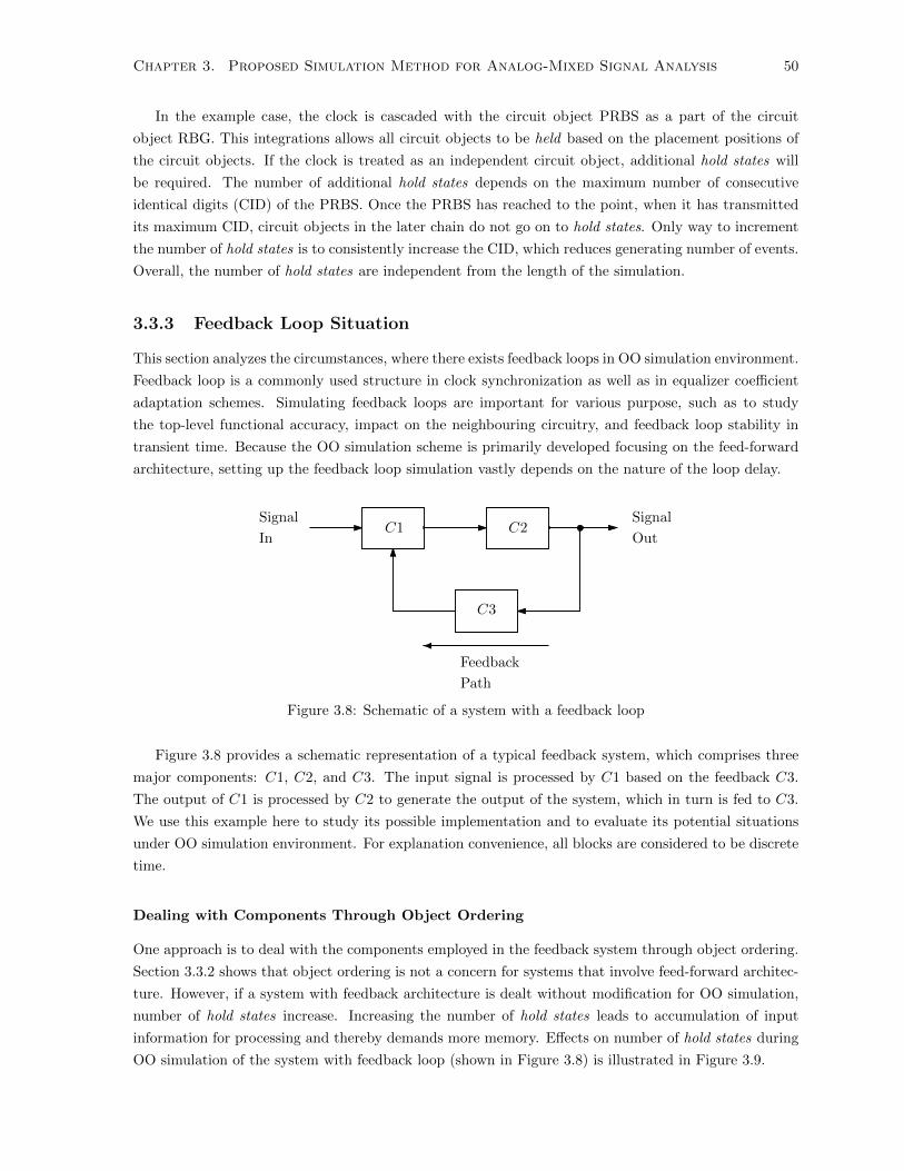
Chapter 3. Proposed Simulation Method for Analog-Mixed Signal Analysis 50
In the example case, the clock is cascaded with the circuit object PRBS as a part of the circuit
object RBG. This integrations allows all circuit objects to be held based on the placement positions of
the circuit objects. If the clock is treated as an independent circuit object, additional hold states will
be required. The number of additional hold states depends on the maximum number of consecutive
identical digits (CID) of the PRBS. Once the PRBS has reached to the point, when it has transmitted
its maximum CID, circuit objects in the later chain do not go on to hold states. Only way to increment
the number of hold states is to consistently increase the CID, which reduces generating number of events.
Overall, the number of hold states are independent from the length of the simulation.
3.3.3 Feedback Loop Situation
This section analyzes the circumstances, where there exists feedback loops in OO simulation environment.
Feedback loop is a commonly used structure in clock synchronization as well as in equalizer coefficient
adaptation schemes. Simulating feedback loops are important for various purpose, such as to study
the top-level functional accuracy, impact on the neighbouring circuitry, and feedback loop stability in
transient time. Because the OO simulation scheme is primarily developed focusing on the feed-forward
architecture, setting up the feedback loop simulation vastly depends on the nature of the loop delay.
Signal
In
Signal
Out
Feedback
Path
C1 C2
C3
Figure 3.8: Schematic of a system with a feedback loop
Figure 3.8 provides a schematic representation of a typical feedback system, which comprises three
major components: C1, C2, and C3. The input signal is processed by C1 based on the feedback C3.
The output of C1 is processed by C2 to generate the output of the system, which in turn is fed to C3.
We use this example here to study its possible implementation and to evaluate its potential situations
under OO simulation environment. For explanation convenience, all blocks are considered to be discrete
time.
Dealing with Components Through Object Ordering
One approach is to deal with the components employed in the feedback system through object ordering.
Section 3.3.2 shows that object ordering is not a concern for systems that involve feed-forward architec-
ture. However, if a system with feedback architecture is dealt without modification for OO simulation,
number of hold states increase. Increasing the number of hold states leads to accumulation of input
information for processing and thereby demands more memory. Effects on number of hold states during
OO simulation of the system with feedback loop (shown in Figure 3.8) is illustrated in Figure 3.9.
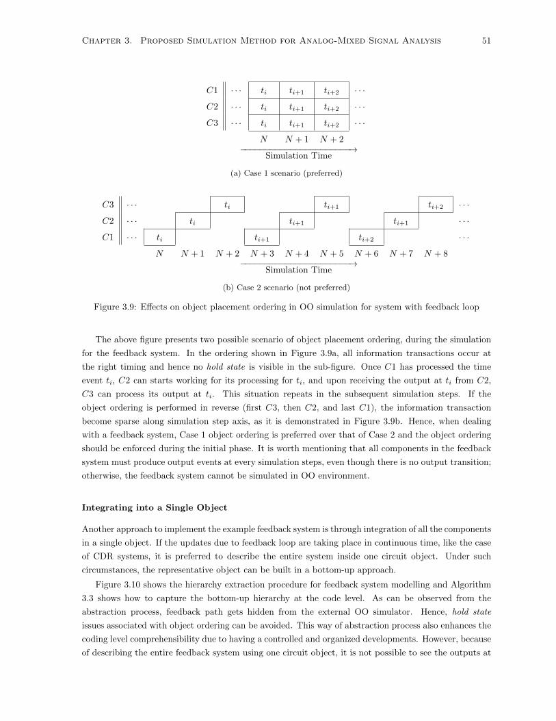
Chapter 3. Proposed Simulation Method for Analog-Mixed Signal Analysis 51
C1 · · · ti ti+1 ti+2 · · ·
C2 · · · ti ti+1 ti+2 · · ·
C3 · · · ti ti+1 ti+2 · · ·
N N + 1 N + 2−−−−−−−−−−−−−−−−−−−−−−→
Simulation Time
(a) Case 1 scenario (preferred)
C3 · · · ti ti+1 ti+2 · · ·
C2 · · · ti ti+1 ti+1 · · ·
C1 · · · ti ti+1 ti+2 · · ·
N N + 1 N + 2 N + 3 N + 4 N + 5 N + 6 N + 7 N + 8−−−−−−−−−−−−−−−−−−−−−−→
Simulation Time
(b) Case 2 scenario (not preferred)
Figure 3.9: Effects on object placement ordering in OO simulation for system with feedback loop
The above figure presents two possible scenario of object placement ordering, during the simulation
for the feedback system. In the ordering shown in Figure 3.9a, all information transactions occur at
the right timing and hence no hold state is visible in the sub-figure. Once C1 has processed the time
event ti, C2 can starts working for its processing for ti, and upon receiving the output at ti from C2,
C3 can process its output at ti. This situation repeats in the subsequent simulation steps. If the
object ordering is performed in reverse (first C3, then C2, and last C1), the information transaction
become sparse along simulation step axis, as it is demonstrated in Figure 3.9b. Hence, when dealing
with a feedback system, Case 1 object ordering is preferred over that of Case 2 and the object ordering
should be enforced during the initial phase. It is worth mentioning that all components in the feedback
system must produce output events at every simulation steps, even though there is no output transition;
otherwise, the feedback system cannot be simulated in OO environment.
Integrating into a Single Object
Another approach to implement the example feedback system is through integration of all the components
in a single object. If the updates due to feedback loop are taking place in continuous time, like the case
of CDR systems, it is preferred to describe the entire system inside one circuit object. Under such
circumstances, the representative object can be built in a bottom-up approach.
Figure 3.10 shows the hierarchy extraction procedure for feedback system modelling and Algorithm
3.3 shows how to capture the bottom-up hierarchy at the code level. As can be observed from the
abstraction process, feedback path gets hidden from the external OO simulator. Hence, hold state
issues associated with object ordering can be avoided. This way of abstraction process also enhances the
coding level comprehensibility due to having a controlled and organized developments. However, because
of describing the entire feedback system using one circuit object, it is not possible to see the outputs at

Chapter 3. Proposed Simulation Method for Analog-Mixed Signal Analysis 52
Signal
In
Signal
OutC1 C2
C3
obj C1
obj C1C2
obj C1C2C3
Figure 3.10: Hierarchical representation for a system with a feedback loop
Algorithm 3.3 Hierarchical representation template for OO simulation
% In obj C1.m fileclassdef obj C1 < handle % Starting as root
- properties and methods are described hereend
% In obj C1C2.m fileclassdef obj C1C2 < obj C1 % Inheriting from obj C1
- properties and methods that are not described in obj C1 go hereend
% In obj C1C2C3.m fileclassdef obj C1C2C3 < obj C1C2 % Inheriting from obj C1C2
- properties and methods that are described neither in obj C1nor in obj C1C2 go here
end
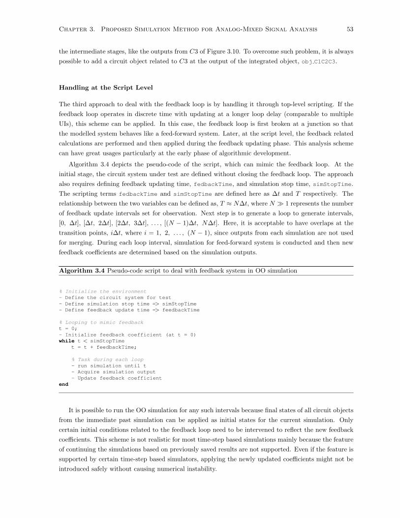
Chapter 3. Proposed Simulation Method for Analog-Mixed Signal Analysis 53
the intermediate stages, like the outputs from C3 of Figure 3.10. To overcome such problem, it is always
possible to add a circuit object related to C3 at the output of the integrated object, obj C1C2C3.
Handling at the Script Level
The third approach to deal with the feedback loop is by handling it through top-level scripting. If the
feedback loop operates in discrete time with updating at a longer loop delay (comparable to multiple
UIs), this scheme can be applied. In this case, the feedback loop is first broken at a junction so that
the modelled system behaves like a feed-forward system. Later, at the script level, the feedback related
calculations are performed and then applied during the feedback updating phase. This analysis scheme
can have great usages particularly at the early phase of algorithmic development.
Algorithm 3.4 depicts the pseudo-code of the script, which can mimic the feedback loop. At the
initial stage, the circuit system under test are defined without closing the feedback loop. The approach
also requires defining feedback updating time, fedbackTime, and simulation stop time, simStopTime.
The scripting terms fedbackTime and simStopTime are defined here as ∆t and T respectively. The
relationship between the two variables can be defined as, T ≈ N∆t, where N 1 represents the number
of feedback update intervals set for observation. Next step is to generate a loop to generate intervals,
[0, ∆t], [∆t, 2∆t], [2∆t, 3∆t], . . . , [(N − 1)∆t, N∆t]. Here, it is acceptable to have overlaps at the
transition points, i∆t, where i = 1, 2, . . . , (N − 1), since outputs from each simulation are not used
for merging. During each loop interval, simulation for feed-forward system is conducted and then new
feedback coefficients are determined based on the simulation outputs.
Algorithm 3.4 Pseudo-code script to deal with feedback system in OO simulation
% Initialize the environment- Define the circuit system for test- Define simulation stop time => simStopTime- Define feedback update time => feedbackTime
% Looping to mimic feedbackt = 0;- Initialize feedback coefficient (at t = 0)while t < simStopTime
t = t + feedbackTime;
% Task during each loop- run simulation until t- Acquire simulation output- Update feedback coefficient
end
It is possible to run the OO simulation for any such intervals because final states of all circuit objects
from the immediate past simulation can be applied as initial states for the current simulation. Only
certain initial conditions related to the feedback loop need to be intervened to reflect the new feedback
coefficients. This scheme is not realistic for most time-step based simulations mainly because the feature
of continuing the simulations based on previously saved results are not supported. Even if the feature is
supported by certain time-step based simulators, applying the newly updated coefficients might not be
introduced safely without causing numerical instability.
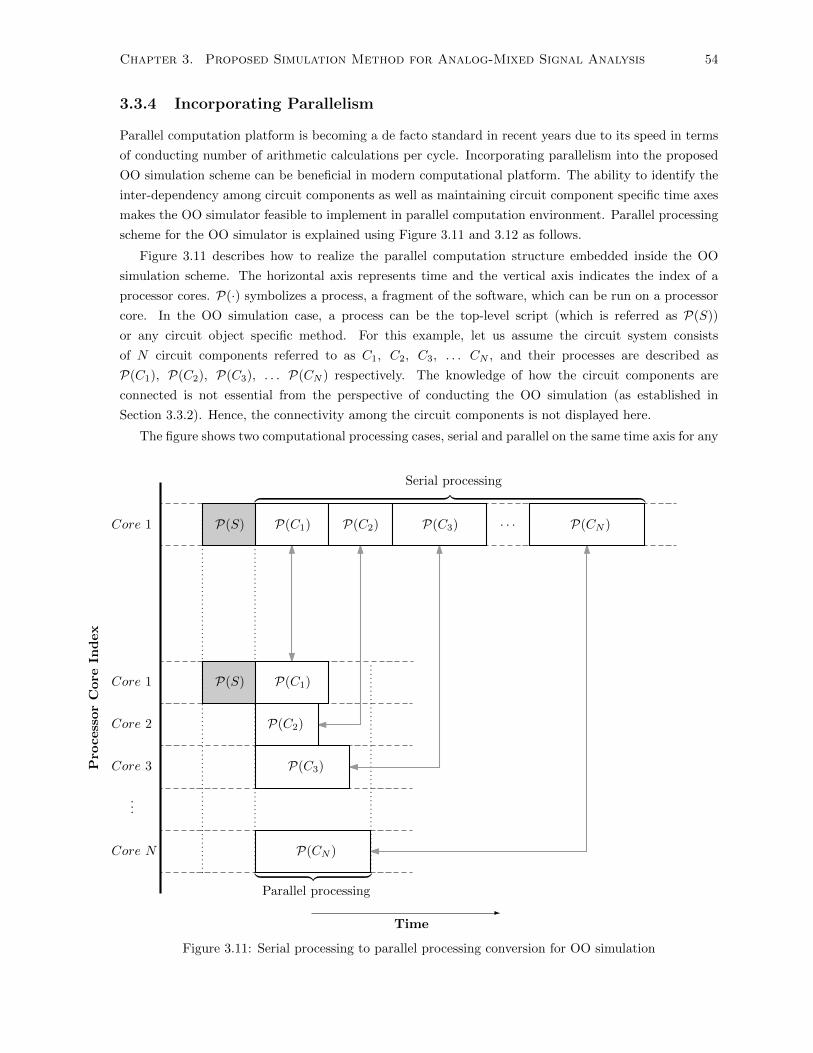
Chapter 3. Proposed Simulation Method for Analog-Mixed Signal Analysis 54
3.3.4 Incorporating Parallelism
Parallel computation platform is becoming a de facto standard in recent years due to its speed in terms
of conducting number of arithmetic calculations per cycle. Incorporating parallelism into the proposed
OO simulation scheme can be beneficial in modern computational platform. The ability to identify the
inter-dependency among circuit components as well as maintaining circuit component specific time axes
makes the OO simulator feasible to implement in parallel computation environment. Parallel processing
scheme for the OO simulator is explained using Figure 3.11 and 3.12 as follows.
Figure 3.11 describes how to realize the parallel computation structure embedded inside the OO
simulation scheme. The horizontal axis represents time and the vertical axis indicates the index of a
processor cores. P(·) symbolizes a process, a fragment of the software, which can be run on a processor
core. In the OO simulation case, a process can be the top-level script (which is referred as P(S))
or any circuit object specific method. For this example, let us assume the circuit system consists
of N circuit components referred to as C1, C2, C3, . . . CN , and their processes are described as
P(C1), P(C2), P(C3), . . . P(CN ) respectively. The knowledge of how the circuit components are
connected is not essential from the perspective of conducting the OO simulation (as established in
Section 3.3.2). Hence, the connectivity among the circuit components is not displayed here.
The figure shows two computational processing cases, serial and parallel on the same time axis for any
Serial processing︷ ︸︸ ︷
Pro
cessorCore
Index
Core 1 P(S) P(C1) P(C2) P(C3) · · · P(CN )
Core 1
Core 2
Core 3
...
Core N
P(S) P(C1)
P(C2)
P(C3)
P(CN )︸ ︷︷ ︸Parallel processing
-Time
Figure 3.11: Serial processing to parallel processing conversion for OO simulation

Chapter 3. Proposed Simulation Method for Analog-Mixed Signal Analysis 55
Pro
cessorCore
Index
Core 1
Core 2
Core 3
Core 4
P(S) P(C1)
P(C2)
P(C3)
P(C4)
P(C5)
P(C6)
P(C7)
· · ·
· · ·
· · · P(CN )
︸ ︷︷ ︸Parallel processing
-Time
Figure 3.12: Parallel processing demonstration under restricted resource environment for OO simulation
given simulation step. Top part of the figure depicts the situation, if the OO simulation is evaluated using
only one core, Core 1. First time slot is utilized to perform the process associated with top-level script,
P(S), where all processes related to circuit components, P(Ci), are launched from. If the computation
platform has access to more cores than the number of processes associated with circuit components
(number of cores ≥ N), all processes, P(Ci), can be launched at the same time upon evaluation of
process, P(S). The gray arrows in the bottom part of the figure demonstrate the parallelism performed
by N processing cores. As can be observed, incorporating parallelism with abundant processing cores is
only limited by the evaluation time of the longest process among all the processes.
Once the circuit system becomes larger, the number of processes associated with circuit components
usually increases. Under such circumstances, the number of processes is much larger than the number of
available processing cores for parallel computations and this is typically expected for current processors
in applications. Figure 3.12 depicts the case of a 4-core processor evaluating previously described N -
component circuit system, where it is assumed N 4. As can be observed from the figure, P(S), is
first performed, and then all P(Ci)’s are evaluated using the 4 cores in parallel.
3.3.5 Simulation Speed Performance
For the simulation performance analysis, we study a test case related to FFE operation as shown in
Figure 3.13. The trasmitter side consists of a RBG (shown as source) followed by an FFE and triggered
by a clock source (shown as TxClk). Once equalized by the FFE, the transmitted signal is then sent
through the attenuating channel (shown as Ch). Continuous time output from the channel is then
analyzed at the scopes to generate the eye diagram and to measure jitter. Detail modelling process of
the FFE circuitry and its various settings are described in Section 4.1.
We implement this test case in detail in C++ using a Linux computer with Intel Core i7 processor.
The source and the FFE along with their clock are implemented as one discrete time circuit object. The
channel is implemented here as a continuous time object and its maximum output time resolution is set
to 0.01 UI (or minimum 100 discrete time points per UI), because its output is fed to an eye scope to
calculate the eye diagram with exactly 0.01 UI resolution. The output of the channel is also fed to a

Chapter 3. Proposed Simulation Method for Analog-Mixed Signal Analysis 56
Transmitter Receiver
Source FFE
TxClk
Ch
Eye
Scope
Jitter
Monitor
(a) Block diagram
Simulation Time for Varying Length
Simulation
Time
1, 000s
100s
10s
1s
0.1s
0.46s
4.40s
43.85s
440.88s
Trend line
10k 100k 1, 000k 10, 000k
Number of Bits (1k = 1000)
(b) Simulation speed result
Figure 3.13: Speed performance result for the OO simulation
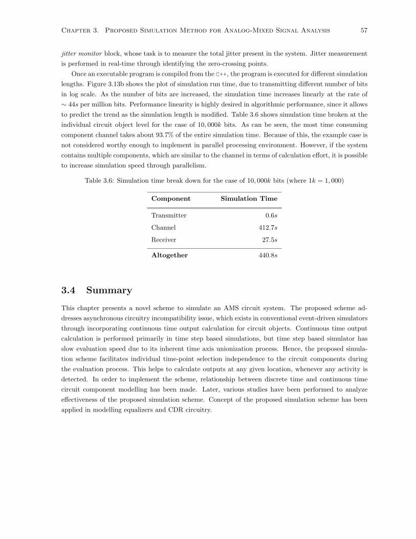
Chapter 3. Proposed Simulation Method for Analog-Mixed Signal Analysis 57
jitter monitor block, whose task is to measure the total jitter present in the system. Jitter measurement
is performed in real-time through identifying the zero-crossing points.
Once an executable program is compiled from the C++, the program is executed for different simulation
lengths. Figure 3.13b shows the plot of simulation run time, due to transmitting different number of bits
in log scale. As the number of bits are increased, the simulation time increases linearly at the rate of
∼ 44s per million bits. Performance linearity is highly desired in algorithmic performance, since it allows
to predict the trend as the simulation length is modified. Table 3.6 shows simulation time broken at the
individual circuit object level for the case of 10, 000k bits. As can be seen, the most time consuming
component channel takes about 93.7% of the entire simulation time. Because of this, the example case is
not considered worthy enough to implement in parallel processing environment. However, if the system
contains multiple components, which are similar to the channel in terms of calculation effort, it is possible
to increase simulation speed through parallelism.
Table 3.6: Simulation time break down for the case of 10, 000k bits (where 1k = 1, 000)
Component Simulation Time
Transmitter 0.6s
Channel 412.7s
Receiver 27.5s
Altogether 440.8s
3.4 Summary
This chapter presents a novel scheme to simulate an AMS circuit system. The proposed scheme ad-
dresses asynchronous circuitry incompatibility issue, which exists in conventional event-driven simulators
through incorporating continuous time output calculation for circuit objects. Continuous time output
calculation is performed primarily in time step based simulations, but time step based simulator has
slow evaluation speed due to its inherent time axis unionization process. Hence, the proposed simula-
tion scheme facilitates individual time-point selection independence to the circuit components during
the evaluation process. This helps to calculate outputs at any given location, whenever any activity is
detected. In order to implement the scheme, relationship between discrete time and continuous time
circuit component modelling has been made. Later, various studies have been performed to analyze
effectiveness of the proposed simulation scheme. Concept of the proposed simulation scheme has been
applied in modelling equalizers and CDR circuitry.

Chapter 4
Proposed Modelling for Equalizer
Circuitry
This chapter discusses the proposed modelling concept for equalizer circuitry. As explained in Section
2.2.1, the task of an equalizer is to compensate for channel attenuation. The primary purpose of proposed
modelling is to speed up the simulation process, while maintaining comparable accuracy to that of
conventional SPICE simulators. Conducting simulations at higher speed and accuracy is required in
order to perform verification analyses, such as generating BER contours (Section 2.3.1).
Three major types of equalizers are analyzed here: feed forward equalizer (FFE), continuous time
linear equalizer (CTLE), and decision feedback equalizer (DFE). Figure 4.1 represents an example ar-
chitecture consisting of these three types of equalizers: FFE at the trasmitter side, while the receiver
contains CTLE and DFE. CTLE is implemented using passive resistive-capacitive circuit elements for
continuous time operation, while FFE and DFE operate in discrete time using local clock sources.
Hence, the figure shows two clock signals, TxClk and RxClk, which are local to the trasmitter and the
receiver respectively, but have uni-directional synchronous relationship. The figure implicitly shows the
synchronous clock relationships, because the clock recovery system is not discussed in this chapter.
Performance of these equalizers often suffers from unavoidable nonlinearities, once they are imple-
mented using real-life circuit elements. The nonlinear effects of the equalizers may appear from various
Transmitter Receiver
Source FFE Ch CTLE DFE Sink
Clock
Synchronization
TxClk RxClk
Figure 4.1: Architectural overview of typical channel equalization system
58

Chapter 4. Proposed Modelling for Equalizer Circuitry 59
sources, such as nonlinear operations, finite bandwidth, mismatches, and process-voltage-temperature
(PVT) variations of transistor and other devices. These nonlinearities limit data communication speed
through transmission channel, but their effects are often not visible in the linear behavioural models of
the respective equalizers. Hence, it is required to capture such nonlinearity as realistically as possible to
increase the accuracy of transceiver performance verification analyses.
This chapter deals with how to capture nonlinear equalizer behaviour in the models. The proposed
modelling schemes for FFE, CTLE, and DFE are presented in Section 4.1, 4.2, and 4.3 respectively. Each
section begins by introducing an equivalent linear model for the corresponding equalizer, then discusses
circuit-level implementation, and finally explains the modelling procedure to capture the transistor-
level nonlinearity. Each proposed model is evaluated through generating an eye diagram (or multiple
eye diagrams depending on the case), which is then overlapped with the one generated by Spectre for
comparison purposes.
4.1 Feed Forward Equalizer (FFE) Modelling
Like any feed-forward control system, FFE equalizes the input signal directly with its pre-conceived
knowledge of the channel attenuation. An FFE can be designed to eliminate both pre-cursor and post-
cursor ISI. FFE, implemented at the trasmitter side, receives input signal from the data transmission
source, which is synchronous to the local clock.
Figure 4.2 shows a block-level architecture of an FFE with M pre-taps and N post-taps. Signal
in represents an input bit-stream, which needs to be transmitted. During the FFE operation, the
multiple delayed versions of the input bit-stream are added with the defined tap weights, wi, where
i = −M, . . . , −1, 0, 1, . . . , N . The z−1 block represents a delay that is usually set to 1 UI. All
the delayed signals and the input signal are first multiplied with their respective tap weights and then
summed up to produce the equalized output.
Signal In · · · · · ·z−1
Delay
z−1 z−1 z−1
w−M w−1 w0 w1 wN
Equalized Output
Figure 4.2: Basic architecture of a symbol-spaced feed forward equalizer (FFE)
Based on this, the FFE transfer function in z-domain, FFFE(z), can be written as follows:
FFFE(z) =
(w−M · zM + · · ·+ w−1 · z︸ ︷︷ ︸
M Pre-taps
+w0 + w1 · z−1 + · · ·+ wN · z−N︸ ︷︷ ︸N Post-taps
)· z−M (4.1)
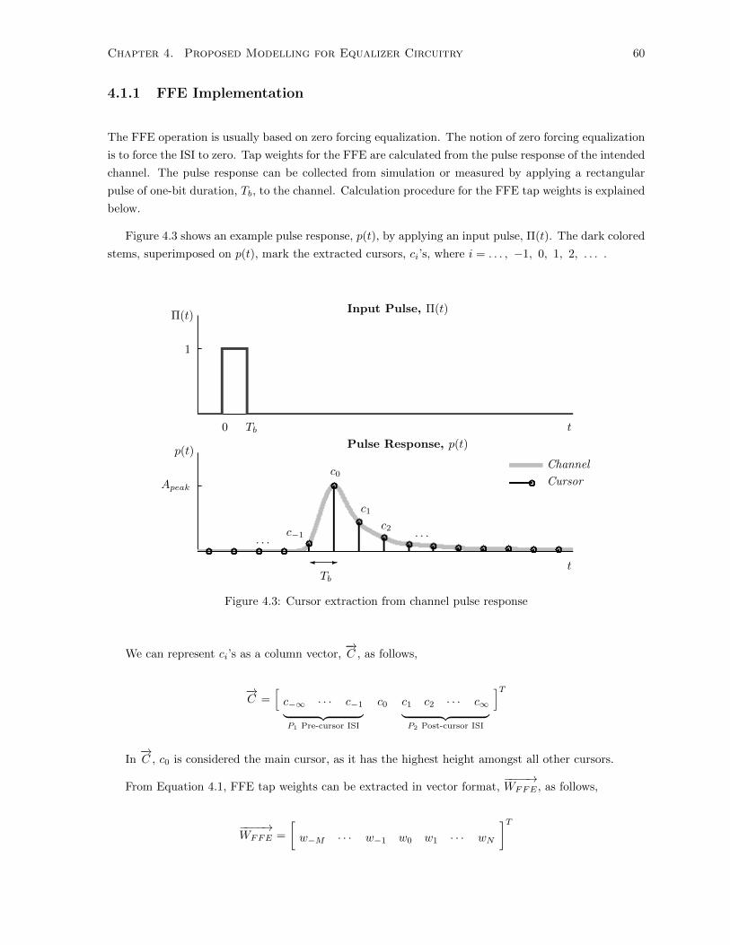
Chapter 4. Proposed Modelling for Equalizer Circuitry 60
4.1.1 FFE Implementation
The FFE operation is usually based on zero forcing equalization. The notion of zero forcing equalization
is to force the ISI to zero. Tap weights for the FFE are calculated from the pulse response of the intended
channel. The pulse response can be collected from simulation or measured by applying a rectangular
pulse of one-bit duration, Tb, to the channel. Calculation procedure for the FFE tap weights is explained
below.
Figure 4.3 shows an example pulse response, p(t), by applying an input pulse, Π(t). The dark colored
stems, superimposed on p(t), mark the extracted cursors, ci’s, where i = . . . , −1, 0, 1, 2, . . . .
Input Pulse, Π(t)Π(t)
1
t0 Tb
Pulse Response, p(t)p(t)
Apeak
t-
Tb
· · ·c−1
c0
c1
c2· · ·
Channel
Cursor
Figure 4.3: Cursor extraction from channel pulse response
We can represent ci’s as a column vector,−→C , as follows,
−→C =
[c−∞ · · · c−1︸ ︷︷ ︸P1 Pre-cursor ISI
c0 c1 c2 · · · c∞︸ ︷︷ ︸P2 Post-cursor ISI
]T
In−→C , c0 is considered the main cursor, as it has the highest height amongst all other cursors.
From Equation 4.1, FFE tap weights can be extracted in vector format,−−−−→WFFE , as follows,
−−−−→WFFE =
[w−M · · · w−1 w0 w1 · · · wN
]T

Chapter 4. Proposed Modelling for Equalizer Circuitry 61
Applying the convolution between−→C and
−−−−→WFFE , the desired channel output response with peak
amplitude, Apeak, can be formulated as follows,
−→C ∗−−−−→WFFE =
[0 0 · · · 0︸ ︷︷ ︸M + P1 zeros
Apeak 0 0 · · · 0︸ ︷︷ ︸N zeros
](4.2)
where
−→C ∗−−−−→WFFE =
... c−∞
c−1. . .
c0. . .
...
c1. . . c−1
...
c2. . . c0 c−1
...
.... . . c1 c0 c−1
. . .
. . . c2 c1 c0. . .
...
... c2 c1. . . c−1
... c2. . . c0
.... . . c1
. . . c2
c∞...
·
w−M
...
w−1
w0
w1
...
w−N
Here, the number of rows and columns for−→C ∗−−−−→WFFE is (P1 + P2 + M + N + 1) and (M + N + 1)
respectively. Solving Equation 4.2 for−−−−→WFFE yields the FFE tap weights of defined size. As for Apeak,
it is considered as 1 here for simplicity.
An example circuitry of a 3-tap FFE implemented at the trasmitter end is shown in Figure 4.4. The
example circuit is a source series terminated (SST) FFE implemented for single-ended data transmission
application. The circuit consists of two major segments: digital logic circuitry and slices of transmit
driver. The digital logic circuitry encodes the data with delay elements, such as z−1 and z−2, and
polarities for the the tap weights, sgn(wi). The task of the slices is to drive the encoded transmit signals
representing the tap weight magnitudes, |wi|. Widths of the PMOS and NMOS transistors, WPi and
WNi, are designed such that their resistances represent the respective tap weights. In order to minimize
reflection through the channel, the net impedance looking from the output of the slices toward supply or
ground should be set to characteristic impedance of the the channel. Even though the example is shown
for 3-tap case (involving 1 pre-tap and 1 post-tap), the number of taps can be extended to represent M
pre-taps and N post-taps. (Regarding detail design procedure of the transmit driver, refer to [35,36].)

Chapter 4. Proposed Modelling for Equalizer Circuitry 62
Data
In
sgn(w−1)
sgn(w0) · z−1
sgn(w1) · z−2
WP1 ∝ |w1|
WN1 ∝ |w1|RT1 ∝
1
|w1|
Slices of FFE Trasmit DriverDigital FFE Logic Circuitry
Equalized
Out
Figure 4.4: Circuit-level overview of a 3-tap source series terminated based single-ended FFE
4.1.2 FFE Modelling for OO Simulation
In OO simulation, FFE implemented at the trasmitter end, is considered as a discrete time object,
ObjTyp.discrete . Algorithm 4.1 presents the FFE template object for running OO simulation. It
has two input sources for operation: clock and RBG; both sources are discrete type. Routines of its
constructor and methods (inti(), receive(), and process()) are programmed following the criteria
described in Section 3.2.1.
In reality, a fabricated FFE behaves nonlinearly and this has various undesirable effects, such as
sampling threshold shift, jitter increase, and signal transition shape asymmetry. They can be generated
from a wide variety of sources, such as FFE implementation architecture, local clock jitter, and power
supply noise. Here, the primary focus of this section is to discuss how to capture the nonlinearity
associated with the FFE implementation architecture.
Architectural nonlinearity in the example circuit (shown in Figure 4.4) is due to the nonlinear tran-
sistor operation. Because equivalent resistance across the drain-source region depends on the volt-
age difference, tap weights realized from the equivalent resistances vary during the FFE operation.
Hence, no closed-form algebraic equation is not available. To overcome the problem, a look up ta-
ble (LUT) based calculation scheme is proposed. In general, if a FFE has n-taps, it can have 2n
. . . 0110100 . . .
Random binarybit-stream
. . . ,−1,+3,+1,−3, . . .
2-tap FFE symbolicstates (shown for 0110)
A+3A+1
A−1A−3
2-tap FFEoutput states
Figure 4.5: Look-up table (LUT) based nonlinearity modelling for FFE
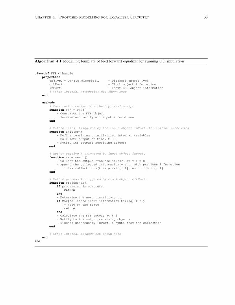
Chapter 4. Proposed Modelling for Equalizer Circuitry 63
Algorithm 4.1 Modelling template of feed forward equalizer for running OO simulation
classdef FFE < handleproperties
objTyp = ObjTyp.discrete - Discrete object TypeclkPort - Clock object informationinPort - Input RBG object information% Other internal properties not shown here
end
methods% Constructor called from the top-level scriptfunction obj = FFE()
- Construct the FFE object- Receive and verify all input information
end
% Method init() triggered by the input object inPort for initial processingfunction init(obj)
- Define remaining uninitialized internal variables- Calculate output at time, t = 0- Notify its outputs receiving objects
end
% Method receive() triggered by input object inPortfunction receive(obj)
- Collect the output from the inPort at t i > 0- Append the collected information v(t i) with previous information
- New collection v(t i) 6= v(t i-1) and t i > t i-1end
% Method process() triggered by clock object clkPortfunction process(obj)
if processing is completedreturn
end- Determine the next transition, t jif Maxcollected input information timing < t j
- Hold on the statereturn
end- Calculate the FFE output at t j- Notify to its output receiving objects- Discard unnecessary inPort outputs from the collection
end
% Other internal methods not shown hereend
end
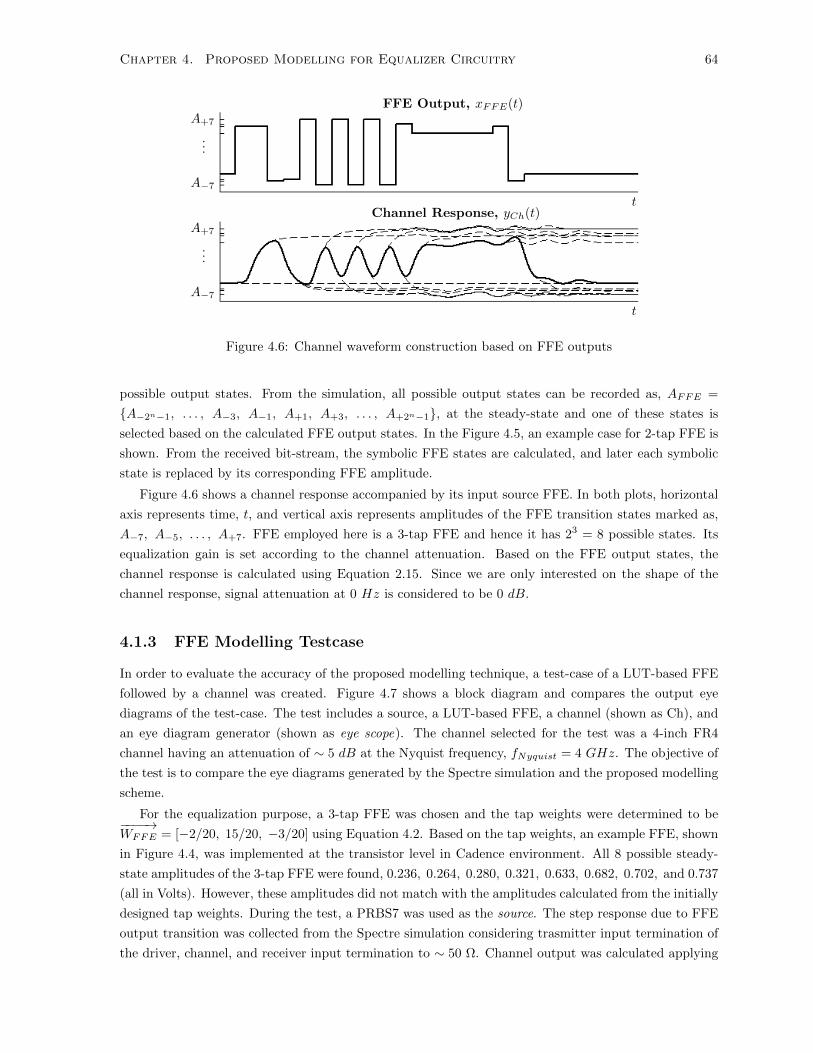
Chapter 4. Proposed Modelling for Equalizer Circuitry 64
FFE Output, xFFE(t)A+7
...
A−7
tChannel Response, yCh(t)
A+7
...
A−7
t
Figure 4.6: Channel waveform construction based on FFE outputs
possible output states. From the simulation, all possible output states can be recorded as, AFFE =
A−2n−1, . . . , A−3, A−1, A+1, A+3, . . . , A+2n−1, at the steady-state and one of these states is
selected based on the calculated FFE output states. In the Figure 4.5, an example case for 2-tap FFE is
shown. From the received bit-stream, the symbolic FFE states are calculated, and later each symbolic
state is replaced by its corresponding FFE amplitude.
Figure 4.6 shows a channel response accompanied by its input source FFE. In both plots, horizontal
axis represents time, t, and vertical axis represents amplitudes of the FFE transition states marked as,
A−7, A−5, . . . , A+7. FFE employed here is a 3-tap FFE and hence it has 23 = 8 possible states. Its
equalization gain is set according to the channel attenuation. Based on the FFE output states, the
channel response is calculated using Equation 2.15. Since we are only interested on the shape of the
channel response, signal attenuation at 0 Hz is considered to be 0 dB.
4.1.3 FFE Modelling Testcase
In order to evaluate the accuracy of the proposed modelling technique, a test-case of a LUT-based FFE
followed by a channel was created. Figure 4.7 shows a block diagram and compares the output eye
diagrams of the test-case. The test includes a source, a LUT-based FFE, a channel (shown as Ch), and
an eye diagram generator (shown as eye scope). The channel selected for the test was a 4-inch FR4
channel having an attenuation of ∼ 5 dB at the Nyquist frequency, fNyquist = 4 GHz. The objective of
the test is to compare the eye diagrams generated by the Spectre simulation and the proposed modelling
scheme.
For the equalization purpose, a 3-tap FFE was chosen and the tap weights were determined to be−−−−→WFFE = [−2/20, 15/20, −3/20] using Equation 4.2. Based on the tap weights, an example FFE, shown
in Figure 4.4, was implemented at the transistor level in Cadence environment. All 8 possible steady-
state amplitudes of the 3-tap FFE were found, 0.236, 0.264, 0.280, 0.321, 0.633, 0.682, 0.702, and 0.737
(all in Volts). However, these amplitudes did not match with the amplitudes calculated from the initially
designed tap weights. During the test, a PRBS7 was used as the source. The step response due to FFE
output transition was collected from the Spectre simulation considering trasmitter input termination of
the driver, channel, and receiver input termination to ∼ 50 Ω. Channel output was calculated applying
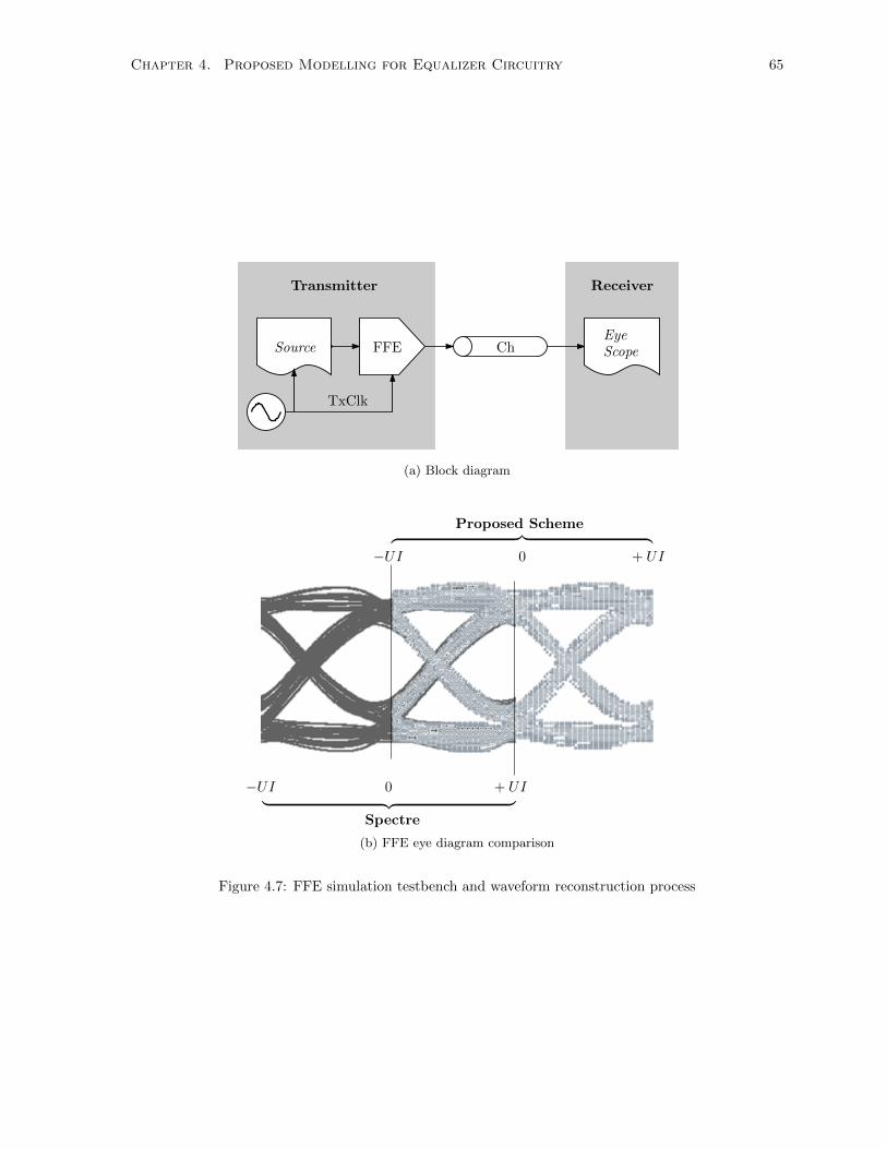
Chapter 4. Proposed Modelling for Equalizer Circuitry 65
Transmitter Receiver
Source FFE ChEyeScope
TxClk
(a) Block diagram
Proposed Scheme︷ ︸︸ ︷−UI 0 + UI
−UI 0 + UI︸ ︷︷ ︸Spectre
(b) FFE eye diagram comparison
Figure 4.7: FFE simulation testbench and waveform reconstruction process
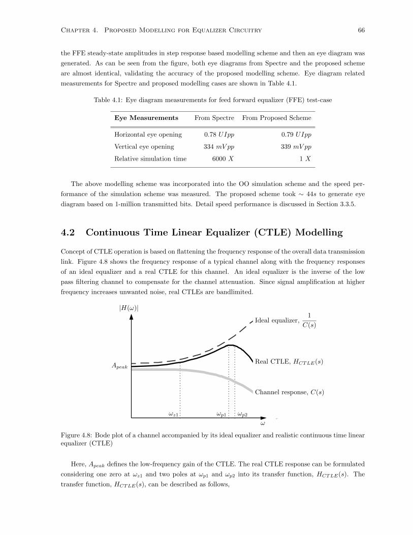
Chapter 4. Proposed Modelling for Equalizer Circuitry 66
the FFE steady-state amplitudes in step response based modelling scheme and then an eye diagram was
generated. As can be seen from the figure, both eye diagrams from Spectre and the proposed scheme
are almost identical, validating the accuracy of the proposed modelling scheme. Eye diagram related
measurements for Spectre and proposed modelling cases are shown in Table 4.1.
Table 4.1: Eye diagram measurements for feed forward equalizer (FFE) test-case
Eye Measurements From Spectre From Proposed Scheme
Horizontal eye opening 0.78 UIpp 0.79 UIpp
Vertical eye opening 334 mV pp 339 mV pp
Relative simulation time 6000 X 1 X
The above modelling scheme was incorporated into the OO simulation scheme and the speed per-
formance of the simulation scheme was measured. The proposed scheme took ∼ 44s to generate eye
diagram based on 1-million transmitted bits. Detail speed performance is discussed in Section 3.3.5.
4.2 Continuous Time Linear Equalizer (CTLE) Modelling
Concept of CTLE operation is based on flattening the frequency response of the overall data transmission
link. Figure 4.8 shows the frequency response of a typical channel along with the frequency responses
of an ideal equalizer and a real CTLE for this channel. An ideal equalizer is the inverse of the low
pass filtering channel to compensate for the channel attenuation. Since signal amplification at higher
frequency increases unwanted noise, real CTLEs are bandlimited.
ω
ωz1 ωp1 ωp2
|H(ω)|
Apeak
Ideal equalizer,1
C(s)
Real CTLE, HCTLE(s)
Channel response, C(s)
Figure 4.8: Bode plot of a channel accompanied by its ideal equalizer and realistic continuous time linearequalizer (CTLE)
Here, Apeak defines the low-frequency gain of the CTLE. The real CTLE response can be formulated
considering one zero at ωz1 and two poles at ωp1 and ωp2 into its transfer function, HCTLE(s). The
transfer function, HCTLE(s), can be described as follows,

Chapter 4. Proposed Modelling for Equalizer Circuitry 67
HCTLE(s) ≈1
C(s)
= K ·s+ ωz1
(s+ ωp1)(s+ ωp2)(4.3)
where C(s) is the channel transfer function, K is the gain factor, defined as, K = Apeak ·
∣∣∣∣∣ωp1ωp2ωz1
∣∣∣∣∣.This transfer function can provide up to 20 dB/dec between ωz1 and ωp1. To achieve higher gain and
advance equalization, more zeros and poles can be incorporated into the transfer function.
4.2.1 CTLE Implementation
For high-speed wire-line application, a CTLE usually is implemented using passive resistive-capacitive
circuit components. An example of a CTLE circuit system is shown in Figure 4.9. Each stage of
the block diagram can be represented as a generic differential buffer block with an impedance transfer
function, Z(s). Each Z(s) is defined for the specific stage according to the stage functionality. Input of
the example CTLE is single-ended, while its output is differential. Due to receiving signal-ended signal,
the input terminal, Vin−, of the gain stage is connected to a reference voltage, Vref , while other input
terminal, Vin+, is connected to the channel attenuated signal, Vin.
Task of the gain stage is to achieve high frequency gain, while the amplification stages are for
providing required amplification for sampling. The impedance transfer function, Z(s), plays a major
role in defining the output characteristics of each stage. For the amplification stages, Z(s)’s are set to
be 0 (or shorted), while for the gain stage, Z(s) is formed using a parallel combination of a resistor, Rz,
and a capacitor, Cz. Applying the definition, the zero, ωz1, and the poles, ωp1 and ωp2, can be found as,
ωz1 =1
RzCz
ωp1 =1
RzCz
1 +gm1 · gm2
gm1 + gm2·Rz
ωp2 =1
RLCL
where gm1 and gm2 represent transconductances of M1 and M2 transistors respectively.
4.2.2 CTLE Modelling for OO Simulation
Since CTLE is usually modelled to observe its eye diagram, its object type is chosen as continuous type,
ObjTyp.Continuous . It can be incorporated as an independent or as part of a cascaded continuous
time filter for OO simulation. Because the goal here is to model its nonlinearity using the step response
based scheme due to the computational speed advantages, any preceding continuous time filters need to

Chapter 4. Proposed Modelling for Equalizer Circuitry 68
Vin
Vref
Vout
Gain stage Amplifying stagesDifferential signal
Single-ended signal
(a) CTLE block diagram
Vin+ Vin−
−Vout+
RL RL
M1 M2
Z(s)
Iss2
Iss2
RL: Load resistanceIss: Tail current
(b) Generic schematic for all stages
Z(s) =
Rz
Cz
Gain stage
Amplifying
stage
(c) Definition of Z(s)
Figure 4.9: Circuit-level overview of single-ended CTLE

Chapter 4. Proposed Modelling for Equalizer Circuitry 69
be cascaded. Figure 4.10 shows such an example case, where the CTLE is cascaded with the channel
(shown as Ch). Here, the source is considered discrete type object, such as RBG and FFE, where the
sink can be any object, such as any measurement scope. Algorithm 4.2 depicts the pseudo-code for
CTLE operation under OO simulation environment.
Transmitter Receiver
Clk
Source Ch CTLE Sink
Cascading Filters
Figure 4.10: Representing CTLE for OO simulation
Even though the functionality of a CTLE is supposed to be linear, CTLE implemented at the circuit-
level shows noticeable nonlinearity. This nonlinearity mostly contributes to often deformed and asym-
metric eye diagrams, which result in high jitter as well as shifted sampling threshold reference. These can
be taken into account in the CTLE model considering the gain nonlinearity as well as system memory,
which are described as follows.
Gain Nonlinearity
Gain nonlinearity is regarded as variation in output signal gain due to different input signal amplitude.
Ideally, the output signal is considered constant for the CTLE, but the nonlinearity is observable from
its circuit-level implementation. Figure 4.11 shows the DC gain plot of a differential buffer like CTLE.
Here, the DC gain is defined as, ∆VOut/∆VIn, where ∆VIn = Vi2 − Vi1, ∆VOut = Vo2 − Vo1, and all
amplitudes, Vi1 and Vi2, can vary independently within the CTLE input signal range. As the input
signal, ∆VIn increases due to Vi1 and Vi2, the output signal, ∆VOut increases with variable gain until it
saturates.
︷ ︸︸ ︷∆VIn
Vi1 Vi2 vIn
︸︷︷
︸
∆VOut
Vo1
Vo2
vOut
Figure 4.11: Plot of CTLE gain response, vOut/vIn

Chapter 4. Proposed Modelling for Equalizer Circuitry 70
Algorithm 4.2 Modeling template of continuous time linear equalizer for running OO simulation
classdef CTLE < handleproperties
objTyp = ObjTyp.continuous - Continuous object TypeinPort - Input circuit object information% Other internal properties not shown here
end
methods% Constructor called from the top-level scriptfunction obj = CTLE
- Construct the CTLE object- Receive and verify all required inputs
end
% Method init() triggered by the input object inPortfunction init(obj)
- Define additional uninitialized internal variables- Calculate the output, y(t = 0)- Notify its outputs receiving objects for collection
end
% Method receive() triggered by the object inPortfunction receive(obj)
- Collect outputs from the input object inPort at t i+1- call its process() method
end
% Method process() called from thefunction process(obj)
- Generate time vector, (t i, t i+1]- Calculate the output, (y(t i), y(t i+1)]- Notify its output receiving objects for collection- Discard unnecessary input information
% Other internal methods not shown hereend
end
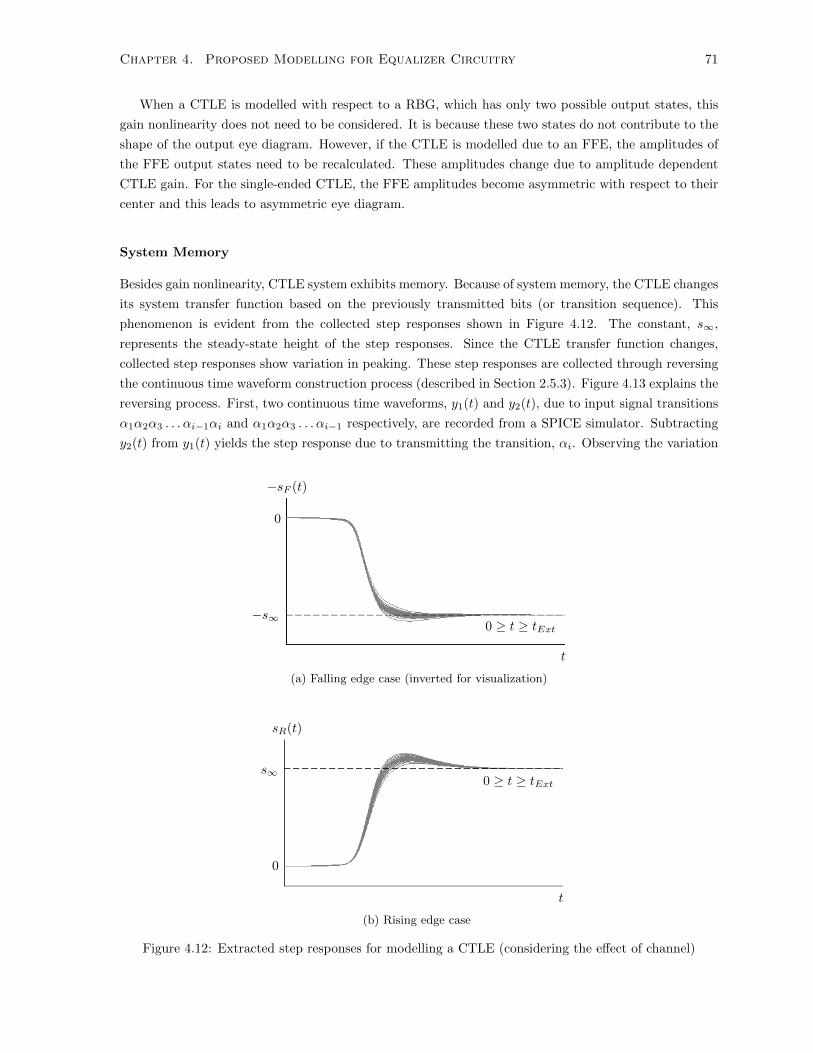
Chapter 4. Proposed Modelling for Equalizer Circuitry 71
When a CTLE is modelled with respect to a RBG, which has only two possible output states, this
gain nonlinearity does not need to be considered. It is because these two states do not contribute to the
shape of the output eye diagram. However, if the CTLE is modelled due to an FFE, the amplitudes of
the FFE output states need to be recalculated. These amplitudes change due to amplitude dependent
CTLE gain. For the single-ended CTLE, the FFE amplitudes become asymmetric with respect to their
center and this leads to asymmetric eye diagram.
System Memory
Besides gain nonlinearity, CTLE system exhibits memory. Because of system memory, the CTLE changes
its system transfer function based on the previously transmitted bits (or transition sequence). This
phenomenon is evident from the collected step responses shown in Figure 4.12. The constant, s∞,
represents the steady-state height of the step responses. Since the CTLE transfer function changes,
collected step responses show variation in peaking. These step responses are collected through reversing
the continuous time waveform construction process (described in Section 2.5.3). Figure 4.13 explains the
reversing process. First, two continuous time waveforms, y1(t) and y2(t), due to input signal transitions
α1α2α3 . . . αi−1αi and α1α2α3 . . . αi−1 respectively, are recorded from a SPICE simulator. Subtracting
y2(t) from y1(t) yields the step response due to transmitting the transition, αi. Observing the variation
−sF (t)
0
−s∞0 ≥ t ≥ tExt
t
(a) Falling edge case (inverted for visualization)
sR(t)
s∞
0
0 ≥ t ≥ tExt
t
(b) Rising edge case
Figure 4.12: Extracted step responses for modelling a CTLE (considering the effect of channel)

Chapter 4. Proposed Modelling for Equalizer Circuitry 72
Waveform Due to Transition Sequence, α1α2 . . . αi−1αi
Waveform Due to Transition Sequence, α1α2 . . . αi−1
Calculated Step Response
y1(t)
y2(t)
y1(t)− y2(t)
0 tExt︸ ︷︷ ︸Extracted region
t
Figure 4.13: Step response extraction process for CTLE
on y1(t)− y2(t), extraction region for the step response is determined.
Here, we propose modelling CTLE using step responses, sF (t) and sR(t), collected from shorter
SPICE simulations. Figure 4.14 shows the construction process of CTLE continuous time waveform,
yCTLE(t). The top plot shows a random bit-stream, x(t), which has transitions at ti (where i = 1, 2, . . . ).
For each transition at ti, a step response is determined based on the approximate output at t′i = ti+ ∆t,
where ∆t denotes a constant time offset. The approximate output at t′i does not exactly follow the CTLE
output, yCTLE(t), since it does not take into account the transitions happening after ti. ∆t is determined
during the step response extraction through observing where variations among step responses are visually
maximum. During the waveform construction, step response determination involves selecting the closest
step response among the collected ones or interpolating one.
The proposed modelling method for CTLE offers several key benefits compared to other modelling
methods. The example single-ended CTLE has asymmetric rising and falling edges leading to deformed
eye diagram. This can be easily taken into considerations in the scheme with two different set of step
responses. Another key advantage is that the nonlinearity conditions of the CTLE need to be determined
only at the transition events instead of every chosen time point. Thus, the proposed modelling scheme
avoids numerous repetitive calculations at every time step unlike the time-step based ODE modelling.
In addition, the proposed modelling scheme considers the memory effect using approximate output of
the CTLE and this provides flexibility to include frequency offset related activities, such as data-rate
variations, random and deterministic jitters. Other memory effect modelling schemes, such as bit-pattern
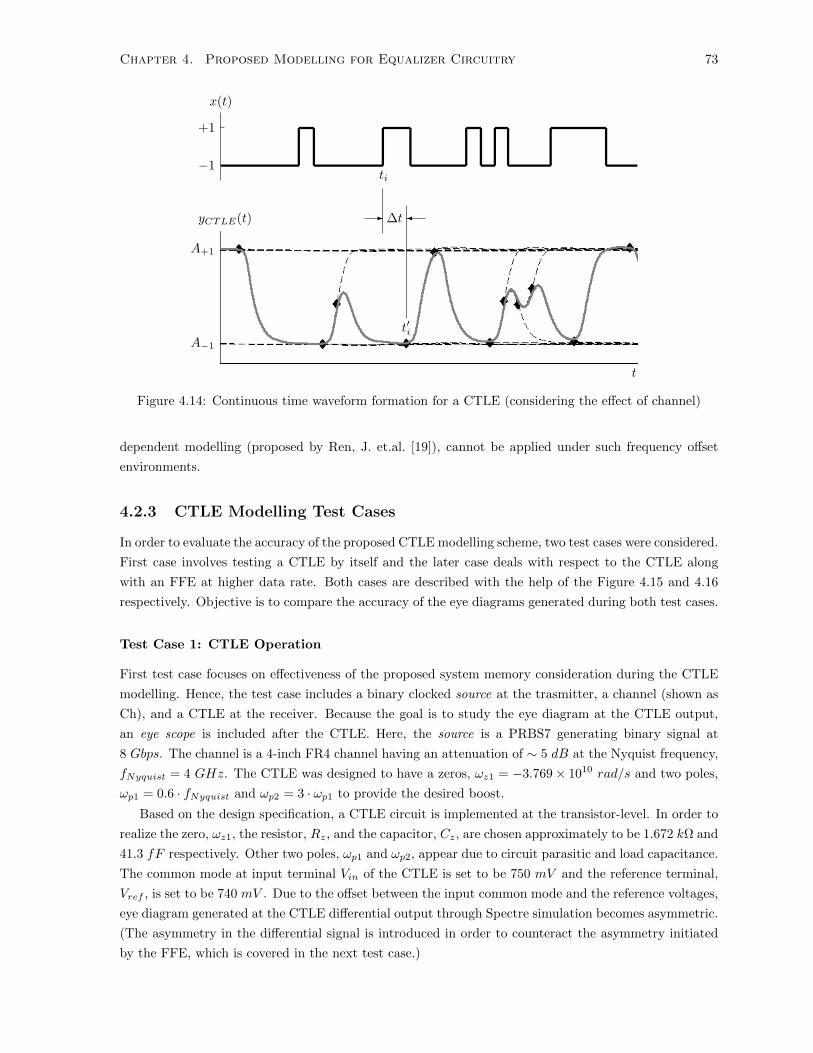
Chapter 4. Proposed Modelling for Equalizer Circuitry 73
x(t)
−1
+1
yCTLE(t)
A+1
A−1
t
ti
- ∆t
t′i
Figure 4.14: Continuous time waveform formation for a CTLE (considering the effect of channel)
dependent modelling (proposed by Ren, J. et.al. [19]), cannot be applied under such frequency offset
environments.
4.2.3 CTLE Modelling Test Cases
In order to evaluate the accuracy of the proposed CTLE modelling scheme, two test cases were considered.
First case involves testing a CTLE by itself and the later case deals with respect to the CTLE along
with an FFE at higher data rate. Both cases are described with the help of the Figure 4.15 and 4.16
respectively. Objective is to compare the accuracy of the eye diagrams generated during both test cases.
Test Case 1: CTLE Operation
First test case focuses on effectiveness of the proposed system memory consideration during the CTLE
modelling. Hence, the test case includes a binary clocked source at the trasmitter, a channel (shown as
Ch), and a CTLE at the receiver. Because the goal is to study the eye diagram at the CTLE output,
an eye scope is included after the CTLE. Here, the source is a PRBS7 generating binary signal at
8 Gbps. The channel is a 4-inch FR4 channel having an attenuation of ∼ 5 dB at the Nyquist frequency,
fNyquist = 4 GHz. The CTLE was designed to have a zeros, ωz1 = −3.769× 10¹⁰ rad/s and two poles,
ωp1 = 0.6 · fNyquist and ωp2 = 3 · ωp1 to provide the desired boost.
Based on the design specification, a CTLE circuit is implemented at the transistor-level. In order to
realize the zero, ωz1, the resistor, Rz, and the capacitor, Cz, are chosen approximately to be 1.672 kΩ and
41.3 fF respectively. Other two poles, ωp1 and ωp2, appear due to circuit parasitic and load capacitance.
The common mode at input terminal Vin of the CTLE is set to be 750 mV and the reference terminal,
Vref , is set to be 740 mV . Due to the offset between the input common mode and the reference voltages,
eye diagram generated at the CTLE differential output through Spectre simulation becomes asymmetric.
(The asymmetry in the differential signal is introduced in order to counteract the asymmetry initiated
by the FFE, which is covered in the next test case.)
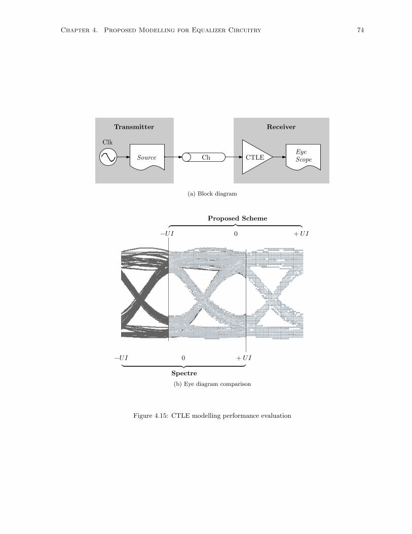
Chapter 4. Proposed Modelling for Equalizer Circuitry 74
Transmitter Receiver
Clk
Source Ch CTLEEyeScope
(a) Block diagram
Proposed Scheme︷ ︸︸ ︷−UI 0 + UI
−UI 0 + UI︸ ︷︷ ︸Spectre
(b) Eye diagram comparison
Figure 4.15: CTLE modelling performance evaluation

Chapter 4. Proposed Modelling for Equalizer Circuitry 75
Following the proposed modelling scheme, the CTLE is then modelled. During the test, since the
CTLE response is calculated due to a binary source, gain nonlinearity is not taken into account. In order
to consider the CTLE system memory, 16 different rising and falling edges are recorded from Spectre
simulations. The extracted step responses are then used to construct the continuous time waveform,
which is later overlaid on top of each other to generate the eye diagram. As can be observed from
the figure, the eye diagrams from the proposed scheme nicely have matched on top of the one from
the Spectre simulation. Table 4.2 shows eye diagram measurements for both Spectre and the proposed
modelling scheme cases.
Table 4.2: Eye diagram measurements for continuous time linear equalizer (CTLE) test-case
Eye Measurements From Spectre From Proposed Scheme
Horizontal eye opening 0.78 UI 0.78 UI
Vertical eye opening 301 mV ppd 300 mV ppd
Relative simulation time1 2000 X 1 X
Test Case 2: FFE-CTLE Joint Operation
Aim of this test case is to demonstrate how to describe the CTLE nonlinearity due to a multi-level
source, such as FFE. Figure 4.16 shows the test case block diagram and the overlapped eye diagrams
for comparison. The test-bench of this case is quite similar to that of the Test Case 1, except that the
transmitted signal being pre-equalized by an FFE. The local clock at the trasmitter (shown as TxClk)
triggers both the source and the FFE.
Here, the data transmission took place at 16 Gbps and the channel has ∼ 20 dB attenuation (at
fNyquist = 8 GHz). Before the transmission, the input bit-stream is equalized by the same 3-tap FFE
described in Section 4.1.3. However, the FFE steady-state transition levels vary from its originally
recorded values, due to the CTLE gain nonlinearity. The newly recorded FFE transition levels are,
−0.570, −0.559, −0.547, −0.483, 0.412, 0.512, 0.541, 0.570, (measurement unit in Volts). Even though
the FFE has 8 different steady states, there are only 14 possible different transitions (instead of 8× (8−1) = 56). For each transition case, 8 different CTLE step responses are considered. The step responses
are applied following the proposed scheme to generate the continuous time waveform, which is then used
to generate an eye diagram. Eye diagrams generated from both Spectre and the proposed scheme are
overlapped and as can be observed, both eye diagrams have matched and measurements related to these
diagrams are presented in Table 4.3.
Table 4.3: Eye diagram measurements for CTLE test-case due to FFE
Eye Measurements From Spectre From Proposed Scheme
Horizontal eye opening 0.71 UIpp 0.69 UIpp
Vertical eye opening 498 mV ppd 501 mV
Relative simulation time1 2000 X 1 X
1Approximated from the speed measurements of the FFE test-case, described in Section 3.3.5
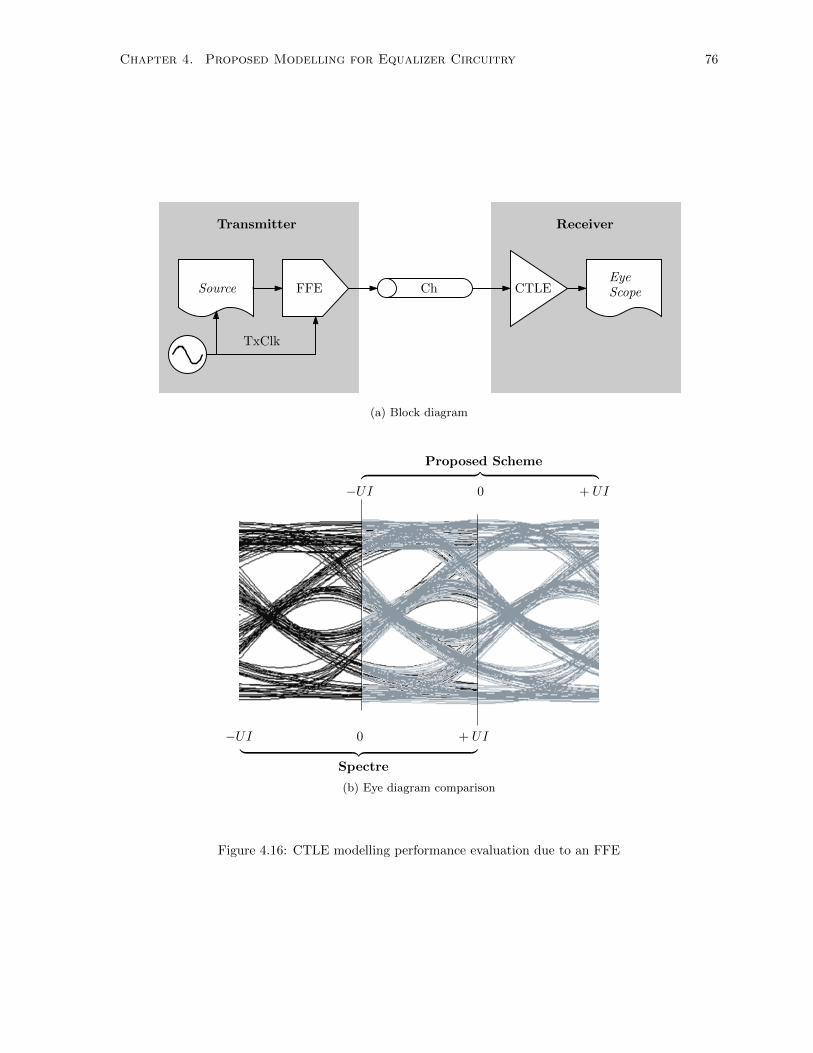
Chapter 4. Proposed Modelling for Equalizer Circuitry 76
Transmitter Receiver
TxClk
Source FFE Ch CTLEEyeScope
(a) Block diagram
Proposed Scheme︷ ︸︸ ︷−UI 0 + UI
−UI 0 + UI︸ ︷︷ ︸Spectre
(b) Eye diagram comparison
Figure 4.16: CTLE modelling performance evaluation due to an FFE

Chapter 4. Proposed Modelling for Equalizer Circuitry 77
4.3 Decision Feedback Equalizer (DFE) Modelling
The DFE operation involves subtracting residual ISI from the channel attenuated signal directly in time
domain and the equalization is usually performed right before data sampling. Residual ISI is determined
based on the previously detected bits and hence this equalizer cannot remove pre-cursor ISI like FFE.
Besides, the DFE has dependency on the local clock supply to calculate the residual ISI and hence its
performance depends on the amount of jitter present in the clock.
Figure 4.17 shows the architecture of a DFE. The DFE consists of three key components: an adder,
a slicer, and a feedback filter. Task of the adder is to subtract residual ISI, ei, calculated in discrete time
(where ei = e(t = ti) and i = 1, 2, 3, . . . ), from the continuous time input signal, x(t). The discrete
time residual ISI, ei, is held on for the bit-duration, Tb, until a new residual ISI, ei+1, is available. The
continuous time output from the adder, y(t), is then sampled by the slicer to determine the transmitted
bits, yi, with respect to an assigned threshold. yi can be any of the valid transmitted bits, yi ∈ −1,+1,for a given threshold 0. The feedback filter is there to calculate the residual ISI, ei using the previously
decided bits, yi’s, as inputs based on the defined tap weights, wi’s, where i = 1, 2, . . . , N .
Signal In,
x(t)
Equalized Output,
yDFE(t)
Decided Bits, yi
Slicer
Feedback Filter
Adder
Delay
z−1 · · · z−1 z−1
wN w2 w1
Res
idu
alIS
I,e i
Figure 4.17: Basic architecture of a decision feedback equalizer
4.3.1 DFE Implementation
Concept of residual ISI subtraction during the DFE operation is explained using Figure 4.18. The DFE
pulse response, pDFE(t), is superimposed on top of the intended channel response, c(t), which is recorded
due to the input pulse, Π(t). Here, the example DFE only cancels two ISI cursors, c1 and c2, followed
by the main cursor, c0 based on the clock sampling phase. As can be observed from pDFE(t), it contains
sharp edges, because the DFE removes the ISI only at the sampling locations due to its discrete time
feedback filter. For high-speed transceiver operation, a slicer is usually implemented using sampling
latch, which requires sufficient sampling aperture (both before and after the sampling clock edge) to
function properly. To ensure proper sampling latch operation, outputs from the filter should be made
available furthest point from the sampling phase; hence, each discontinuity in pDFE(t) appears around

Chapter 4. Proposed Modelling for Equalizer Circuitry 78
Input Pulse, Π(t)
t0 Tb
1
Channel and DFE Response
t-Tb
Apeak
c0
c1c2
Channel, c(t)
Cursor, ci
DFE, pDFE(t)
Figure 4.18: Pulse response due to 2-tap decision feedback equalizer (DFE)
at a middle point between two neighbouring cursors.
At the circuit level, a DFE employs an analog adder accompanied by a digitally clocked slicer and a
feedback FIR filter. The example DFE used for modelling study both receives and provides differentially
ended signals in order to comply with the differential output of the CTLE presented earlier. Figure 4.19
provides circuit-level overview of the DFE of interest. The DFE adder is realized using multiple gain
blocks with shared resistive load, RL, in order to perform current-mode summation. Each gain block is
a differential pair transistor, M1 and M2, biased with a current source, Iss,i, which is set proportional
to the corresponding tap weight, wi, where i = 0, 1, 2, . . . , N . The slicer is designed using a DFF with
high input sensitivity in order to achieve greater amplification for low equalized signal. Output of the
DFF is then fed to digital FIR logic to determine the polarity and delay of the gain stage, Ai. Here,
the rising edge of the clock is considered as sampling phase for the DFF and the falling edge is used for
digital FIR logic operation.
4.3.2 DFE Modelling for OO Simulation
Depending on the simulation requirements, a DFE can be considered as either a discrete time circuit
object, ObjTyp.discrete or a continuous time circuit object, ObjTyp.continuous . If the simulation
objective is only to acquire the recovered bits, modelling the DFE as a discrete time object is usually
sufficient. However, if generating eye diagrams is the ultimate goal, the DFE needs to be considered as a
continuous time circuit object. During the simulation, a DFE accepts two inputs: a clock source, which
is discrete type, and a signal source for equalization. If the DFE is modelled using an adder with linear
gain and infinite bandwidth, the signal source should be a continuous time circuit object such as channel
and CTLE. In contrast, if a realistic adder is incorporated, DFE modelling scheme becomes similar to
that of the CTLE. For step response based modelling, any continuous time filter along the signal source
path needs to be cascaded. Algorithm 4.3 presents the pseudo-code for a DFE as a continuous time

Chapter 4. Proposed Modelling for Equalizer Circuitry 79
Equalized Signal Decided Binary BitsSignal
In
Clock
RL RL
A0
A1
. . .
AN
D Q
D Q
DFF
Digital
FIR
Logic
(a) Top-level
+ +Vin IoutAi− −
Symbol View
+
Vin
−
+
Iout
−
M1 M2
Iss,i ∝ Ai
Schematic View
(b) Gain Block Description
Figure 4.19: Circuit-level overview of differentially ended DFE

Chapter 4. Proposed Modelling for Equalizer Circuitry 80
circuit object. Like an FFE, the DFE also operates synchronously with the local clock. Hence, methods
for the DFE are programmed similarly to those of the FFE.
Algorithm 4.3 Modeling template of decision feedback equalizer for running OO simulation
classdef DFE < handleproperties
objTyp = ObjTyp.continuous - Continuous object TypeclkPort - Clock object informationinPort - Data source object information% Other internal properties not shown here
end
methods% Constructor called from the top level scriptfunction obj = DFE
- Construct the circuit object DFE- Receive and verify all required input information
end
% Method init() triggered by data source object, inPortfunction init(obj)
- Define additional uninitialized internal variables- Calculate the output at t = 0- Notify its output receiving objects for initial output collection
end
% Method receive() triggered by data source object, inPortfunction receive(obj)
- Collect outputs from object pointed by inPort at (t i-1, t i]- Append the outputs to previously stored information
end
% Method process() triggered by clock object, clkPortfunction process(obj)
if processing is completedreturn
end- Get the clock transition, t jif Maxcollected output timing of inPort < t j
- Hold on to the state at t jreturn
end- Determine next processing time range, (t j-1, t j]- Calculate the output for the range- Notify its output receiving objects for output collection- Discard unnecessary input information
end
% Other internal methods not shown hereend
end
Output calculation for the DFE is similar to that of the CTLE due to algorithmic similarity. Figure
4.20 shows how to modify the DFE block diagram in order to capture the finite bandwidth property
for step response based modelling. A DFE top-level block diagram with a bandlimited adder, where
a LPF with transfer function, HAdder(s), is incorporated after the adder block. The HAdder(s) block
is shifted before the adder and it causes to have two HAdder(s) blocks: one along the signal path and
another closed to the FFIR(z) block. The HAdder(s) block along signal path needs to be cascaded with
its preceding continuous time filter blocks, such as channel and CTLE. Other HAdder(s) block is applied

Chapter 4. Proposed Modelling for Equalizer Circuitry 81
Signal
In, x(t)
Decided
Bits, yi
Bandlimited Adder
Adder
HAdder(s)
Slicer
FFIR(z)
(a) Conventional model
Signal
In, x(t)
Decided
Bits, yi
AdderSlicer
HAdder(s)
HAdder(s)
FFIR(z)
(b) Considering adder bandwidth before the addition
Figure 4.20: Modifying DFE model to capture the finite adder bandwidth
to convert the discrete time output of the feedback filter, FFIR(z). This allows to consider the adder as
an ideal summer, since its inputs are bandlimited.
Like CTLE, gain nonlinearity and system memory need to be taken into account for the DFE adder.
Initially, all DFE steady-states and their state transitions are identified due to input signal source as
well as its feedback filter as part of the gain nonlinearity modelling. In order to capture system memory,
multiple step responses are recorded with their associated intermediate output information. In the case,
one set of such information is associated with the cascaded continuous time filters along the signal path
and the other set is related to the HAdder(s) from the FFIR(z). These collected information are then
applied to construct the continuous time DFE output. Because the proposed modelling scheme for
DFE shares great similarity with that of the CTLE, the aforementioned modelling advantages are also
retained.
4.3.3 DFE Modelling Test Case
Based on the proposed DFE modelling scheme, a testcase is designed to evaluate the modelling accuracy.
Figure 4.21 depicts the testbench and the eye diagram comparison. The block diagram is quite similar
to typical top-level equalization architecture (Figure 4.1). As can be inferred from the testbench, all
equalizers (FFE, CTLE, and DFE) are considered during this test. Here, the data transmission is set at

Chapter 4. Proposed Modelling for Equalizer Circuitry 82
Transmitter Receiver
Source FFE Ch CTLE DFEEyeScope
DelayBuffer
TxClkRxClk
(a) Block diagram
Proposed Scheme︷ ︸︸ ︷−UI 0 + UI
−UI 0 + UI︸ ︷︷ ︸Spectre
(b) Eye diagram comparison
Figure 4.21: DFE modelling performance evaluation with respect to FFE and CTLE

Chapter 4. Proposed Modelling for Equalizer Circuitry 83
16 Gbps and the selected channel (show as Ch) is 4-inch FR4 with an insertion loss of ∼ 20 dB at the
Nyquist frequency, fNyquist = 8 GHz. An eye scope is added to observe the eye diagram after combined
equalization of FFE, CTLE, and DFE. The receiver clock (shown as RxClk) is created by delaying the
trasmitter clock (shown as as TxClk) instead of incorporating a clock synchronization scheme, because
the objective is only to capture the equalizer nonlinearity in the eye diagram.
In order to equalize for ∼ 20 dB channel attenuation, gains from all equalizers are distributed. For the
test, same 3-tap FFE and the first order CTLE are employed, which are described in Section 4.1.3 and
4.2.3 respectively. After the FFE-CTLE equalization, 1-tap DFE is employed to eliminate the remaining
ISI. Tap weights for the DFE is set up as−−−−→WDFE = [9/12,−3/12], which provides additional ∼ 6 dB
gain. Considering all equalizers, an eye diagram is generated using outputs from Spectre simulation.
In order to achieve the Spectre-like eye diagram, the DFE step responses and their associated pa-
rameters were extracted. Here, 3-tap FFE and 1-tap DFE together contribute to 23 × 21 = 16 possible
steady-states, which were extracted from Spectre simulation, as −0.654, −0.652, −0.650, −0.635, −0.310,
−0.309, −0.308, −0.300, 0.273, 0.300, 0.304, 0.307, 0.588, 0.638, 0.645, and 0.650 (all measured in Volts).
For 16 possible states, 22 different types of step responses are identified and for each type, 4 different step
responses were extracted. Applying step responses, a eye diagram for the DFE are constructed, which
was compared with that generated from the Spectre simulation. As can be seen from the figure, both
eye diagrams nicely overlapped with nearly all eye diagram features. Table 4.4 presents eye diagram
related measurements for both cases.
Table 4.4: Eye diagram measurements for decision feedback equalizer (DFE) test-case
Eye Measurements From Spectre From Proposed Scheme
Horizontal eye opening 0.79 UIpp 0.77 UIpp
Vertical eye opening 470 mV ppd 440 mV ppd
Relative simulation time1 3000 X 1 X
4.4 Summary
This chapter discusses modelling of three types of equalizers: FFE, CTLE, and DFE, in an integrated
environment. For each equalizer, the relationship between the linear step response based modelling and
nonlinear behaviour is established with some modifications. After the modifications, when the linear
step response based modelling has been applied on the equalizers, the proposed modelling is able to
generate eye diagrams, which matches indistinguishably with the eye diagrams generated from Spectre.
The proposed modelling method not only shows excellence in generating accurate eye diagrams but also
demonstrates potentials in simulation speed up, which has been performed on the FFE modelling case.
1Approximated from the speed measurements of the FFE test-case, described in Section 3.3.5
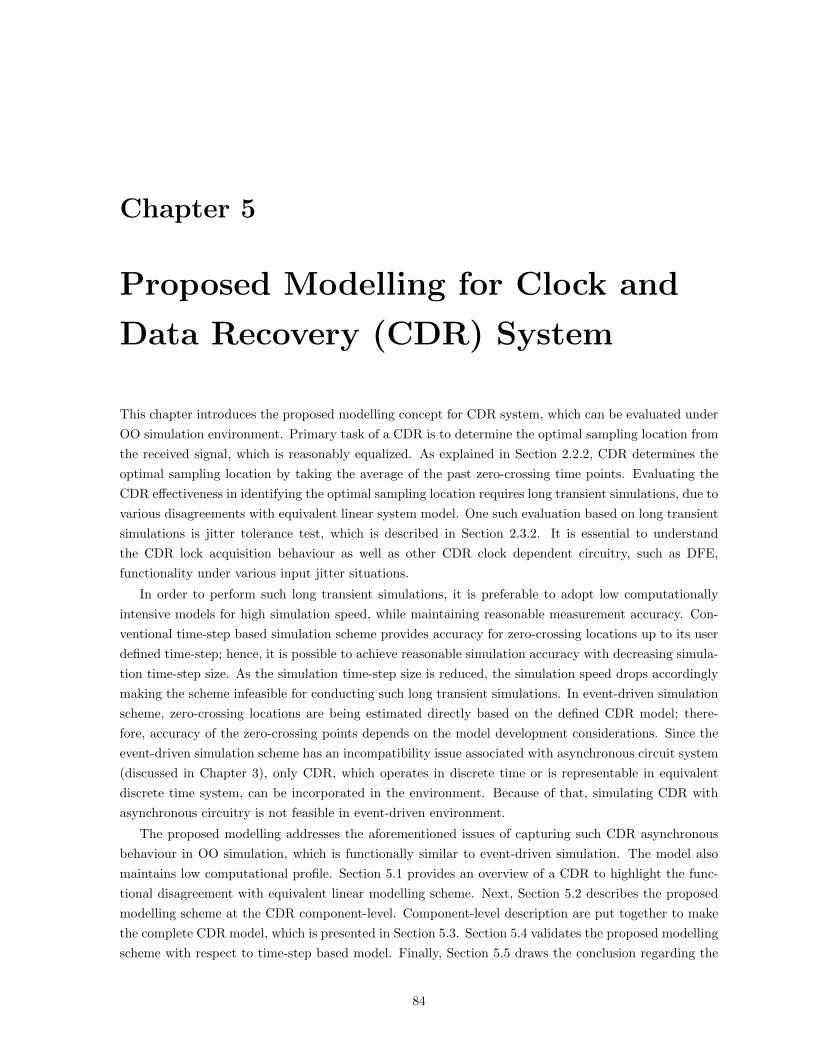
Chapter 5
Proposed Modelling for Clock and
Data Recovery (CDR) System
This chapter introduces the proposed modelling concept for CDR system, which can be evaluated under
OO simulation environment. Primary task of a CDR is to determine the optimal sampling location from
the received signal, which is reasonably equalized. As explained in Section 2.2.2, CDR determines the
optimal sampling location by taking the average of the past zero-crossing time points. Evaluating the
CDR effectiveness in identifying the optimal sampling location requires long transient simulations, due to
various disagreements with equivalent linear system model. One such evaluation based on long transient
simulations is jitter tolerance test, which is described in Section 2.3.2. It is essential to understand
the CDR lock acquisition behaviour as well as other CDR clock dependent circuitry, such as DFE,
functionality under various input jitter situations.
In order to perform such long transient simulations, it is preferable to adopt low computationally
intensive models for high simulation speed, while maintaining reasonable measurement accuracy. Con-
ventional time-step based simulation scheme provides accuracy for zero-crossing locations up to its user
defined time-step; hence, it is possible to achieve reasonable simulation accuracy with decreasing simula-
tion time-step size. As the simulation time-step size is reduced, the simulation speed drops accordingly
making the scheme infeasible for conducting such long transient simulations. In event-driven simulation
scheme, zero-crossing locations are being estimated directly based on the defined CDR model; there-
fore, accuracy of the zero-crossing points depends on the model development considerations. Since the
event-driven simulation scheme has an incompatibility issue associated with asynchronous circuit system
(discussed in Chapter 3), only CDR, which operates in discrete time or is representable in equivalent
discrete time system, can be incorporated in the environment. Because of that, simulating CDR with
asynchronous circuitry is not feasible in event-driven environment.
The proposed modelling addresses the aforementioned issues of capturing such CDR asynchronous
behaviour in OO simulation, which is functionally similar to event-driven simulation. The model also
maintains low computational profile. Section 5.1 provides an overview of a CDR to highlight the func-
tional disagreement with equivalent linear modelling scheme. Next, Section 5.2 describes the proposed
modelling scheme at the CDR component-level. Component-level description are put together to make
the complete CDR model, which is presented in Section 5.3. Section 5.4 validates the proposed modelling
scheme with respect to time-step based model. Finally, Section 5.5 draws the conclusion regarding the
84
Chapter 5. Proposed Modelling for Clock and Data Recovery (CDR) System 85
modelling concept.
5.1 CDR Functional Overview
A CDR contains three major components: phase detector (PD), loop filter (LF), and voltage controlled
oscillator (VCO). Block diagram and linear model of the CDR are shown in Figure 5.1. PD determines
if the clock edges of the CDR (referred to as recovered clock) is early or late with respect to the received
data edges (of signal in as shown in the diagram). Upon detecting a data transition, the PD raises either
early or late flag (shown as E/L referring to early or late case); otherwise, it maintains a no action state
when no adjustment should be taken place. Output of the PD (early, late, or no action), which is a
discrete time signal, is then low pass filtered using the LF to determine the average. Average of early-late
pulse modulated signal is utilized to determine whether the VCO should increase or decrease the output
clock frequency. Recovered data sampled from the input signal is also available from the PD. It is usually
Signal In
Recovered Data
Recovered Clock
PD LF VCOE/L
PD: Phase Detector
LF: Loop Filter
VCO: Voltage Controlled Oscillator
E/L: Early or Late
(a) Block diagram
Phase Detector
KPD HLF (s)KV CO
s
ΦIn(s) VPD VLF ΦOut(s)
(b) Linear model
Figure 5.1: Architectural overview of the clock and data recovery (CDR) system

Chapter 5. Proposed Modelling for Clock and Data Recovery (CDR) System 86
implemented using the data sampling DFFs.
In the linear model, the PD is viewed as a summer that calculates phase difference between the input
signal, ΦIn(s), and the recovered clock output, ΦOut(s), multiplied by a gain factor, KPD. Value of the
PD gain factor, KPD, depends on various factors, such as data transition density, PD architecture, and
ambient noise. Output of the PD, VPD, is then low pass filtered with transfer function, HLF (s), which
is a behavioural representation of the LF. Finally, the HLF (s) output, VLF , is integrated with a gain
factor of KV CO to generate the recovered clock output, Φout(s).
The linear model is employed during the initial design phase to determine parameters for various
circuit components, such as resistors, capacitors, and charge pump switches. This model essentially
helps to initiate the CDR design process based on given constraints, such as loop filter bandwidth,
feedback loop stability, and maximum transient overshoot. However, the model fails to assess the true
reality behind CDR operation, which can easily lead to an implementation failure. Typically, the PD
implemented in a CDR for high-speed application provides discrete time outputs (early, late, or no
action) at designated clock or data transitions, whereas the PD inside the linear model provides phase
difference in continuous time. Every time the PD detects a data transition, it raises a flag causing
the VCO frequency to increase or decrease by a defined constant amount. If the PD requested VCO
frequency offset is set to be so high (or low) to meet the loop filter bandwidth specification that correction
from the PD to reverse VCO frequency offset becomes late and under such circumstance, CDR adds a
wrong sample (or lost a sample). This CDR lock slipping event due to the discreteness of the PD is not
always visible with the continuous time model of the PD in the linear model case. Hence, it is essential
to perform the transient simulation of the CDR, which takes into account the discrete time behaviour
of the PD.
5.2 CDR Component-level Modelling
OO simulation scheme behaves similar to event-driven simulation to achieve speed advantage. During
the OO simulation, CDR is treated as a clock transition event generator. The resultant outputs are
discrete time clock events calculated based on the received input signal. However, the CDR architecture
has a feedback loop, which involves updating in continuous time and hence, it is modelled as one circuit
object (as explained in Section 3.3.3).
Inside the CDR circuit object, the event calculation process is divided into two major segments.
Former segment involves determining the PD output transitions, and the later one deals with LF and
VCO operations. Here, the outputs from the PD and VCO are discrete type, while the LF provides
continuous time output. Since the goal is to determine the clock transition events associated with
the CDR, the LF is cascaded with VCO in order to hide its continuous time information. Cascading
continuous time filters allows to avoid implementing ODE based algorithms, which are computationally
intensive.
5.2.1 Phase Detector (PD) Modelling
Objective of the PD is to generate information related to phase difference between incoming data transi-
tion and CDR clock edges. Usually, two types of PD are mostly found in high-speed applications. They
are: binary PD and linear PD. Detail modelling procedure accompanied by their behavioural functions
are described as follows.
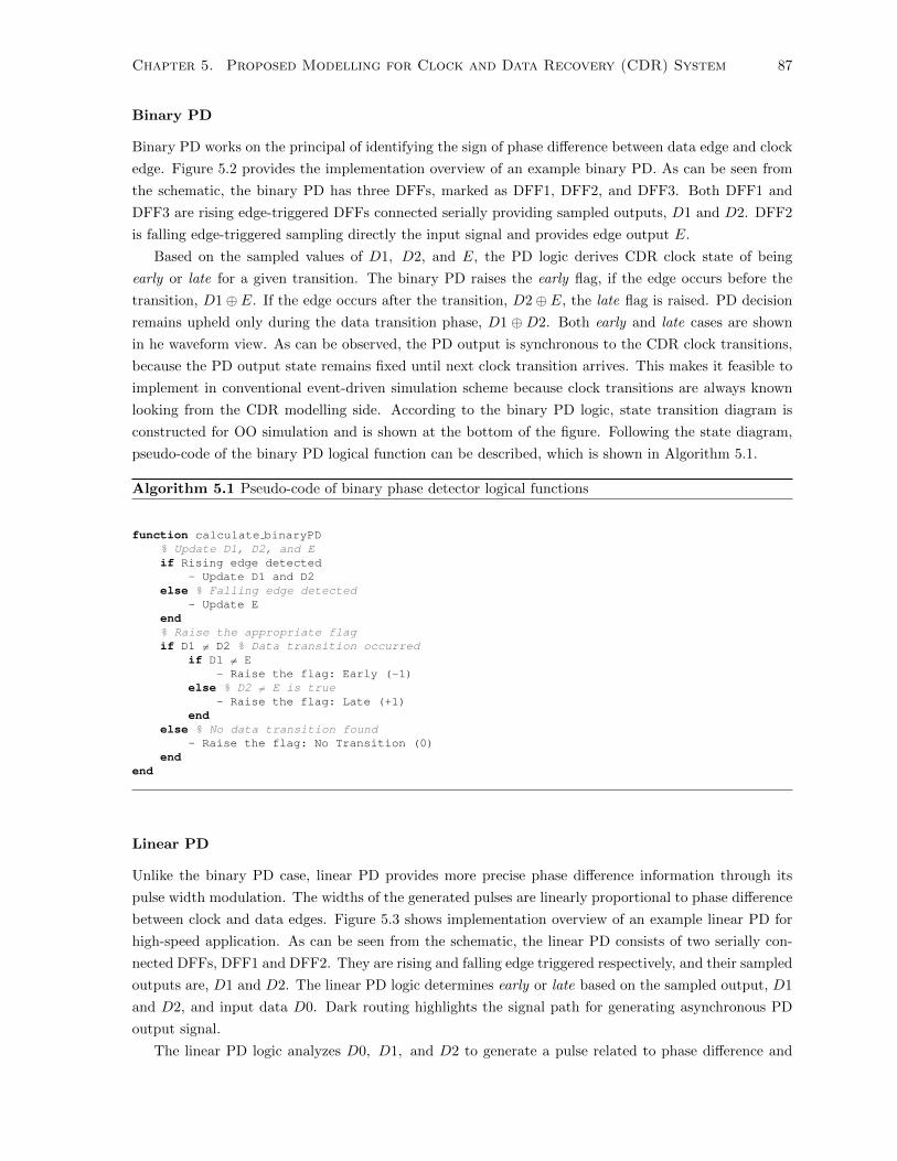
Chapter 5. Proposed Modelling for Clock and Data Recovery (CDR) System 87
Binary PD
Binary PD works on the principal of identifying the sign of phase difference between data edge and clock
edge. Figure 5.2 provides the implementation overview of an example binary PD. As can be seen from
the schematic, the binary PD has three DFFs, marked as DFF1, DFF2, and DFF3. Both DFF1 and
DFF3 are rising edge-triggered DFFs connected serially providing sampled outputs, D1 and D2. DFF2
is falling edge-triggered sampling directly the input signal and provides edge output E.
Based on the sampled values of D1, D2, and E, the PD logic derives CDR clock state of being
early or late for a given transition. The binary PD raises the early flag, if the edge occurs before the
transition, D1⊕ E. If the edge occurs after the transition, D2⊕ E, the late flag is raised. PD decision
remains upheld only during the data transition phase, D1 ⊕ D2. Both early and late cases are shown
in he waveform view. As can be observed, the PD output is synchronous to the CDR clock transitions,
because the PD output state remains fixed until next clock transition arrives. This makes it feasible to
implement in conventional event-driven simulation scheme because clock transitions are always known
looking from the CDR modelling side. According to the binary PD logic, state transition diagram is
constructed for OO simulation and is shown at the bottom of the figure. Following the state diagram,
pseudo-code of the binary PD logical function can be described, which is shown in Algorithm 5.1.
Algorithm 5.1 Pseudo-code of binary phase detector logical functions
function calculate binaryPD% Update D1, D2, and Eif Rising edge detected
- Update D1 and D2else % Falling edge detected
- Update Eend% Raise the appropriate flagif D1 6= D2 % Data transition occurred
if D1 6= E- Raise the flag: Early (-1)
else % D2 6= E is true- Raise the flag: Late (+1)
endelse % No data transition found
- Raise the flag: No Transition (0)end
end
Linear PD
Unlike the binary PD case, linear PD provides more precise phase difference information through its
pulse width modulation. The widths of the generated pulses are linearly proportional to phase difference
between clock and data edges. Figure 5.3 shows implementation overview of an example linear PD for
high-speed application. As can be seen from the schematic, the linear PD consists of two serially con-
nected DFFs, DFF1 and DFF2. They are rising and falling edge triggered respectively, and their sampled
outputs are, D1 and D2. The linear PD logic determines early or late based on the sampled output, D1
and D2, and input data D0. Dark routing highlights the signal path for generating asynchronous PD
output signal.
The linear PD logic analyzes D0, D1, and D2 to generate a pulse related to phase difference and

Chapter 5. Proposed Modelling for Clock and Data Recovery (CDR) System 88
Data In
Clock
DFF1
DFF2
DFF3
D1
D2
E BinaryPD
Logic
PDOut
(a) Schematic view
Early Case
D2 E D1
Late Case
D2 E D1
Data1
0
Clock1
0
PD+1
0−1
Early: −1, Late: +1, No Action: 0
(b) Early/late case waveform
0start
−1
+1
AB
C
B
A
C
C
A
B
A = D1⊕D2
B = (D1⊕D2) · (D1⊕ E)
C = (D1⊕D2) · (D2⊕ E)
(c) State transition
Figure 5.2: Modelling overview of binary phase detector (PD)

Chapter 5. Proposed Modelling for Clock and Data Recovery (CDR) System 89
Linear PD Logic
DFF1 DFF2
D0 D1 D2
Datain
Dataout
PDout
Clock
(a) Schematic viewEarly Case Late Case
Data1
0
Clock1
0
PD
+1
0
−1︸ ︷︷ ︸1 UI
︸ ︷︷ ︸1 UI
Early: −1, Late: +1, No Action: 0
(b) Early/late waveform view
0start
+1
−1
TT
T
T
T
T
(c) State transition
Figure 5.3: Modelling overview of linear PD
Chapter 5. Proposed Modelling for Clock and Data Recovery (CDR) System 90
a pulse of half a UI width for reference. Example PD output waveforms for both early and late cases
are shown in the middle sub-figure. Subtracting the two pulse provides both sign and magnitude of the
desired phase difference for a specific data edge. As can be seen, the early case generates net negative
pulse, whereas the late case generates net positive pulse. It is also worth mentioning from the waveform
that the linear PD output contains additional transitions related to data edges (marked with dotted
vertical lines).
In order to capture the linear PD behaviour, state transition diagram is formed. Typically, once data
transition is detected, T , the PD state transition follows, 0 → +1 → −1 → 0 → · · · path. Unexpected
data transition may take place due to large frequency offset and to cover that, two additional paths,
+1 → 0 and −1 → +1 are drawn. If no data transition is detected, T , the PD remains at the 0 state.
Based on the state transition diagram, pseudo-code for the linear PD is written in Algorithm 5.2. The
algorithm should be called whenever any transition related to data and clock occurs.
Algorithm 5.2 Pseudo-code of linear phase detector logical functions
function calculate linearPD% Update D1, D2if Data transition detected
- Update D0elseif Rising edge detected
- Update D1else % Falling edge detected
- Update D2end% Raise the appropriate flag- Determine the state using (D0 6= D1) - (D1 6= D2)
end
The asynchronous behaviour of the linear PD is due to the additional output transition related to
data edges. These transitions are not directly predictable from the CDR modelling point of view. When
the linear PD based CDR arrives at its lock position, falling edge of the clock tends to align with the
unpredictable data edges. At this phase, the CDR clock edges sometimes comes slightly earlier and other
times sightly later than the data edges. Because of this unpredictable nature of the linear PD, the system
cannot be directly simulated in event-driven simulation. [20] attempted to deal with the unpredictable
transition events for linear PD based phase locked loop (PLL) through isolating PLL related transition
from the actual event-driven simulation time axis. However, the scheme will becomes complicated, if
a similar system needs to be developed for the CDR case, since the system accepts transition events
related to random bit-stream. In order to deal with the aforementioned situation, the OO simulation
with event scheduling flexibility is proposed. Details regarding how to deal with such asynchronous
events are explained earlier in Section 3.3.1.
5.2.2 Loop Filter (LF) and Voltage Controlled Oscillator (VCO) Modelling
Based on the PD generated discrete time outputs, LF and VCO jointly estimate the desired clock
transitions for CDR. Figure 5.4 shows schematic and block diagram overview of charge pump based LF
connected to a VCO. CDR with charge pump based loop filter behaves like a type 2 PLL [37,38]. Because
CDR needs to generate clock, whose phase should be controllable for incoming data edge alignment with
respect to reasonable frequency offset, type 2 PLL mechanism is adopted to track ramp input with zero
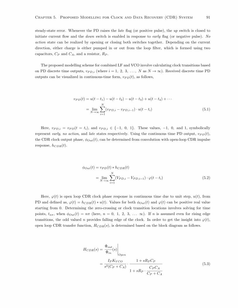
Chapter 5. Proposed Modelling for Clock and Data Recovery (CDR) System 91
steady-state error. Whenever the PD raises the late flag (or positive pulse), the up switch is closed to
initiate current flow and the down switch is enabled in response to early flag (or negative pulse). No
action state can be realized by opening or closing both switches together. Depending on the current
direction, either charge is either pumped in or out from the loop filter, which is formed using two
capacitors, CP and CA, and a resistor, RP .
The proposed modelling scheme for combined LF and VCO involve calculating clock transitions based
on PD discrete time outputs, vPD,i (where i = 1, 2, 3, . . . , N as N →∞). Received discrete time PD
outputs can be visualized in continuous-time form, vPD(t), as follows,
vPD(t) = u(t− t1)− u(t− t2)− u(t− t3) + u(t− t4) + · · ·
= limN→∞
N∑i=1
(vPD,i − vPD,i−1) · u(t− ti) (5.1)
Here, vPD,i = vPD(t = ti), and vPD,i ∈ −1, 0, 1. These values, −1, 0, and 1, symbolically
represent early, no action, and late states respectively. Using the continuous time PD output, vPD(t),
the CDR clock output phase, φOut(t), can be determined from convolution with open-loop CDR impulse
response, hCDR(t).
φOut(t) = vPD(t) ∗ hCDR(t)
= limN→∞
N∑i=1
(VPD,i − VPD,i−1) · ϕ(t− ti) (5.2)
Here, ϕ(t) is open loop CDR clock phase response in continuous time due to unit step, u(t), from
PD and defined as, ϕ(t) = hCDR(t) ∗ u(t). Values for both φOut(t) and ϕ(t) can be positive real value
starting from 0. Determining the zero-crossing or clock transition locations involves solving for time
points, tnπ, when φOut(t) = nπ (here, n = 0, 1, 2, 3, . . . ∞). If n is assumed even for rising edge
transitions, the odd valued n provides falling edge of the clock. In order to get the insight into ϕ(t),
open loop CDR transfer function, HCDR(s), is determined based on the block diagram as follows.
HCDR(s) =Φout
Φin(s)
∣∣∣∣∣Open
=IPKV CO
s2(CP + CA)·
1 + sRPCP
1 + sRP ·CPCA
CP + CA
(5.3)

Chapter 5. Proposed Modelling for Clock and Data Recovery (CDR) System 92
Up
Down
IP
IP
︸ ︷︷ ︸Chargepump
Loop filter
RP
CP
CA
VCO
(a) Schematic view
Chargepump
Up/Down IP
Loop filter
HLF (s)
VCO
KV CO
s
Clockout
HLF (s) =1
s(CP + CA)·
1 + sRPCP
1 + sRP ·CPCA
CP + CA
(b) Block diagram
Figure 5.4: Modeling overview of charge pump based loop filter (LF) and voltage controlled oscillator(VCO)
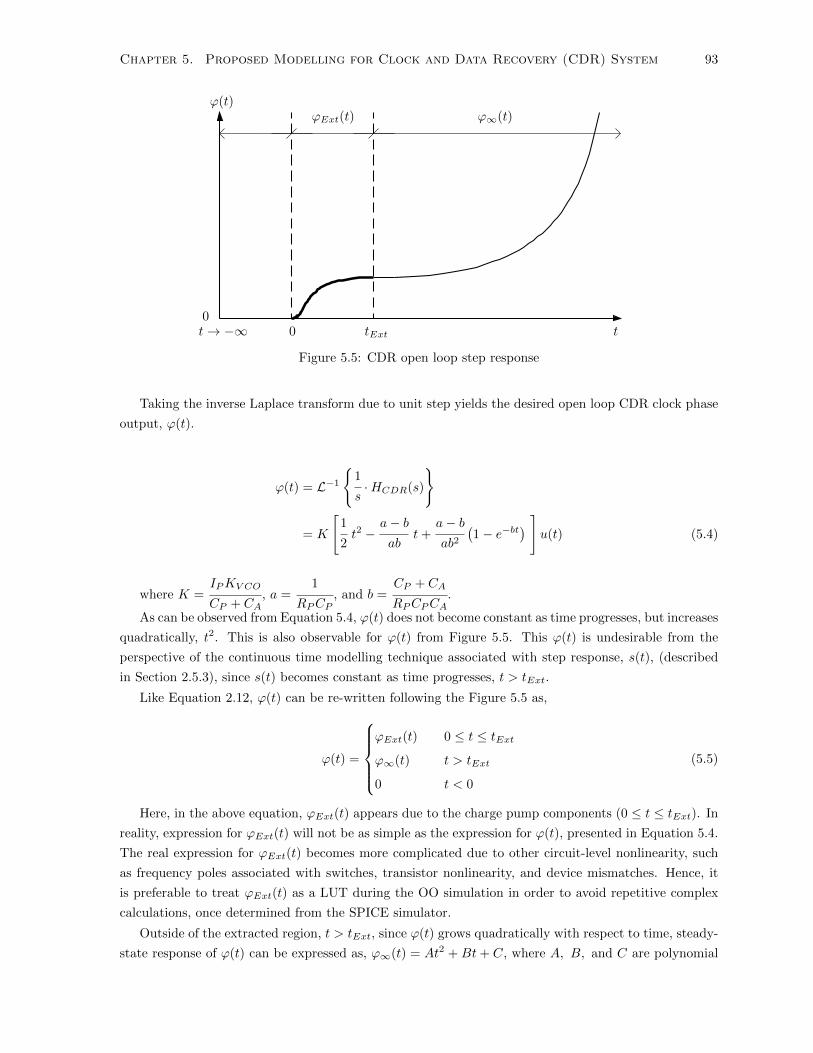
Chapter 5. Proposed Modelling for Clock and Data Recovery (CDR) System 93
ϕ(t)ϕExt(t) ϕ∞(t)
0t→ −∞ 0 tExt t
Figure 5.5: CDR open loop step response
Taking the inverse Laplace transform due to unit step yields the desired open loop CDR clock phase
output, ϕ(t).
ϕ(t) = L−1
1
s·HCDR(s)
= K
[1
2t2 −
a− bab
t+a− bab2
(1− e−bt
) ]u(t) (5.4)
where K =IPKV CO
CP + CA, a =
1
RPCP, and b =
CP + CA
RPCPCA.
As can be observed from Equation 5.4, ϕ(t) does not become constant as time progresses, but increases
quadratically, t2. This is also observable for ϕ(t) from Figure 5.5. This ϕ(t) is undesirable from the
perspective of the continuous time modelling technique associated with step response, s(t), (described
in Section 2.5.3), since s(t) becomes constant as time progresses, t > tExt.
Like Equation 2.12, ϕ(t) can be re-written following the Figure 5.5 as,
ϕ(t) =
ϕExt(t) 0 ≤ t ≤ tExtϕ∞(t) t > tExt
0 t < 0
(5.5)
Here, in the above equation, ϕExt(t) appears due to the charge pump components (0 ≤ t ≤ tExt). In
reality, expression for ϕExt(t) will not be as simple as the expression for ϕ(t), presented in Equation 5.4.
The real expression for ϕExt(t) becomes more complicated due to other circuit-level nonlinearity, such
as frequency poles associated with switches, transistor nonlinearity, and device mismatches. Hence, it
is preferable to treat ϕExt(t) as a LUT during the OO simulation in order to avoid repetitive complex
calculations, once determined from the SPICE simulator.
Outside of the extracted region, t > tExt, since ϕ(t) grows quadratically with respect to time, steady-
state response of ϕ(t) can be expressed as, ϕ∞(t) = At2 +Bt+ C, where A, B, and C are polynomial

Chapter 5. Proposed Modelling for Clock and Data Recovery (CDR) System 94
coefficients. The real VCO does not increase its oscillating frequency linearly, as its input voltage
increases. Usually, the VCO becomes saturated as the input voltage is increased and there also exists
certain amount of delay response time for the VCO to its frequency. Depending the VCO frequency
saturation capturing range, values for A, B, and C can be fitted accordingly using least-square method.
After applying the new definition of ϕ(t) (described in Equation 5.5), CDR clock phase output,
φOut(t), can be expressed as follows,
φOut(t) = limN→∞
N∑i=1
(vPD,i − vPD,i−1) · ϕ(t− ti)
= limN→∞
N∑i=N−k+1
(vPD,i − vPD,i−1) · ϕExt(t− ti) + limN→∞
N−k∑i=1
(vPD,i − vPD,i−1) · ϕ∞(t− ti)︸ ︷︷ ︸φConst(t), Simulation length dependent, O(N 2)
(5.6)
Unlike the Equation 2.15, the second segment marked as φConst(t) still remains as a function of time,
t. If this segment remains time-varying, the implemented algorithm performance will degrade as the
simulation time length increase, O(N 2), which is clearly not desirable. In order to achieve the linear
computational performance, O(N ), like that of the step response based modelling scheme, time-varying
nature of φConst(t) needs to be handled algebraically such that it can be calculated for any given time
space. Since the steady-state ϕ∞(t) can be described with a quadratic expression, ϕ∞(t) = At2+Bt+C,
plugging the expression into the φConst(t) leads as follows,
φConst(t) = limN→∞
N−k∑i=1
(vPD,i − vPD,i−1) · ϕ∞(t− ti)
= limN→∞
N−k∑i=1
(vPD,i − vPD,i−1) ·[A(t− ti)2 +B(t− ti) + C
]
= limN→∞
N−k∑i=1
(vPD,i − vPD,i−1) ·[A B C
]·
1 −2ti t2i
1 −ti
1
︸ ︷︷ ︸
3×3 Constant Matrix, O(N )
·
t2
t
1
(5.7)
As it can be observed from the new expression for φConst(t) in Equation 5.7, the summation ranging
i = 1, 2, . . . N−k, (as N →∞) only incorporates discrete time information associated with PD output
transitions, ti’s. The expression does not include the actual continuous time information, t, whose spread
can be described as, [0, tStop], where tStop indicates simulation stop time.
Like the case of the step response based modelling, first expression in Equation 5.6 involves k number
of summations, which also facilitates simulation length independence, O(N ). The second expression,
φConst(t), has been modified so that only the 3× 3 matrix comprises of ti needs to be updated. Hence,
the second expression also has the similar characteristics like that of the step response case and the
computational complexity is also O(N ).

Chapter 5. Proposed Modelling for Clock and Data Recovery (CDR) System 95
5.3 Putting it Altogether
Since task of the CDR is to generate clock transitions synchronized to optimal sampling location at
the receiver end, the CDR is modelled as a discrete time circuit object, ObjTyp.discrete in OO
simulation environment. CDR accepts only one input associated with binary input sources like RBG.
Depending on the CDR architecture and test objectives, input source for CDR can be discrete time or
continuous time circuit object. If the selected CDR architecture employs linear PD, the CDR input
source should be discrete type, since certain PD transitions are originated from the transitions of the
input source. Sometimes sampling correctness of the DFFs of the PD is important for simulation and
under such circumstance, the CDR can be modelled to accept input from a continuous time circuit object.
Algorithm 5.3 depicts a generic template for coding both linear and binary PD based CDR. Here, linear
PD based CDR operation is explained for OO simulation purpose due to its inherent asynchronous
behaviour causing incompatibility for event-driven simulation environment. Later, a brief discussion on
incorporating binary PD is also provided.
Determining the CDR clock transitions, which is performed inside the method recieve(), requires
simultaneously dealing with the PD output and LF-VCO discrete time transitions. Figure 5.6 is employed
here to explain the proposed CDR clock output transition determination scheme for linear PD based
CDR. After receiving newly processed information, ti+1, from the CDR input circuit object, the CDR
method receive() appends the information with previously received information, ti – this creates an
analysis window, [ti, ti+1), within which the CDR algorithm can determine its output transitions. Let
assume the within the analysis window, [ti, ti+1), N + 1 CDR clock transition occurs. At first, the
linear PD output is determined at the time point, ti, which is associated with the data point transition.
Taking into account the PD output transitions and previous clock transition, tj−1 (where tj−1 < ti),
the proposed scheme defines a new analysis sub-window, [ti, tj + δt). In the new analysis sub-window,
tj represents as new clock transition to be detected and δt defines a small offset necessary to determine
the new transition. Within the newly defined window, continuous time output for LF-VCO is calculated
(mostly around time tj) and from the output, the new transition, tj , is detected through interpolation
at nπ. At this point, the PD output state is updated again at tj . Similar continuous time output for
LF-VCO is performed for new sub-window, [tj , tj+1 + δt) to detect the next clock transition at tj+1.
After that, again the PD output state is updated. This PD state updating as well as new clock transition
detection continue until the final sub-window, [tj+N , ti+1), has been reached. The final sub-window,
[tj+N , ti+1), appears after detecting the last clock transition, tj+N , and analyzing the window does not
provide any new transitions. It is worth mentioning that the PD will not change its state after tj+1 time
event until ti+1 and hence the final sub-window can be selected as [tj+1, ti+1) to detect remaining the
CDR clock transitions.
As can be observed, the proposed modelling scheme take the advantage of event scheduling flexibility
from the OO simulation technique. The event scheduling flexibility has facilitated here to schedule
events, tj , tj+1, tj+2, . . . , tj+N , to take place after estimating data transition event, ti+1, even though
the data transition event, ti+1, occurs later in signal time space. Maintaining the ascending order of time
events, tj < tj+1 < tj+2 < · · · < tj+N < ti+1, is not necessary, since the data transition event, ti+1, is
not going to change due to any variation in the CDR operation. Besides, the event scheduling flexibility
has allowed to avoid inevitable repetitive the entire system calculation elimination in order to detect the
clock transitions. The proposed modelling scheme can also be applied for binary PD based CDR. In that
case, the PD outputs related to data transitions do not take place; otherwise, the modelling for both
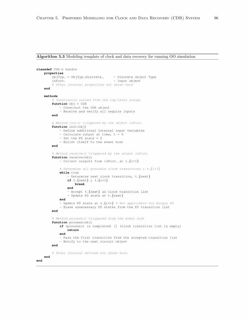
Chapter 5. Proposed Modelling for Clock and Data Recovery (CDR) System 96
Algorithm 5.3 Modeling template of clock and data recovery for running OO simulation
classdef CDR < handleproperties
objTyp = ObjTyp.discrete - Discrete object TypeinPort - Input object% Other internal properties not shown here
end
methods% Constructor called from the top-level scriptfunction obj = CDR
- Construct the CDR object- Receive and verify all require inputs
end
% Method init() triggered by the object inPortfunction init(obj)
- Define additional internal input variables- Calculate output at time, t = 0- Set the PD state = 0- Enlist itself to the event host
end
% Method receive() triggered by the object inPortfunction receive(obj)
- Collect outputs from inPort at t i+1
% Determine all possible clock transitions ≤ t i+1while true
- Determine next clock transition, t nextif t next ≥ t i+1
breakend- Accept t next as clock transition list- Update PD state at t next
end- Update PD state at t i+1 % Not applicable for Binary PD- Erase unnecessary PD states from the PD transition list
end
% Method process() triggered from the event hostfunction process(obj)
if (process() is completed) | | (clock transition list is empty)return
end- Pass the first transition from the accepted transition list- Notify to the next circuit object
end
% Other internal methods not shown hereend
end

Chapter 5. Proposed Modelling for Clock and Data Recovery (CDR) System 97
Data Eye (One or Multiple UIs)
2 consecutive transitions
Intermediate Calculation Steps
tj + δt
tj+1 + δt
. . .
Reconstructed Outputs
PDoutput· · ·Clockoutput
· · ·
ti ti+1
tj−1 tj tj+1 · · · tj+N
Figure 5.6: Demonstration of CDR clock transition calculation

Chapter 5. Proposed Modelling for Clock and Data Recovery (CDR) System 98
linear and binary PD based CDRs share the same modelling procedure. It also indicates more advanced
mixed signaling scheme can be described using the proposed CDR modelling concept.
5.4 Performance Evaluation for the Proposed Modelling Scheme
The proposed step response based modelling scheme for CDR clock transitions in OO simulation envi-
ronment is compared here with the conventional time-step based modelling scheme. The object of the
comparison test is to evaluate its modelling accuracy with the conventional scheme, before performing
additional modification to capture the CDR nonlinearity due to charge pump assisted LF-VCO sat-
uration as well as DFF regeneration effects from PD. Linear PD based CDR is selected for the test
case.
Transmitter Receiver
Clk
Source Ch CDR BERT
Figure 5.7: Test case block diagram for linear PD based CDR
Figure 5.7 shows the testbench employed here to verify the accuracy of the proposed modelling
scheme. Based on the block diagram, the trasmitter end employs only a clock (marked as Clk) syn-
chronous source, which generates PRBS7 bit-stream (marked as source) at 10 Gbps. Then the source
output is passed through the channel (shown as Ch). Here, the channel only adds controlled delay, ∆t,
without initiating any attenuation, since the test-case is not designed to include any jitter effect due to
equalizer. The receiver side comprises only with the linear PD based CDR followed by bit error rate tester
(BERT) for PRBS7. The CDR is designed here with a loop filter bandwidth, ωLF = 20π × 106 rad/s
with a phase margin of 53.1. Based on the system specification, the CDR circuit design parameters are
determined as, IP = 20 µA, CP = 156.3 pF , RP = 1.6 kΩ, CA = 15.6 pF , KV CO = 3.1416 G · rad/s−V(considering input VCO range to be 2V ), and KPD = 0.5/2π (following linear CDR model).
Using the design parameters, the testbench (shown in Figure 5.7) was set up both in time-step based
and OO simulation environments. Both types of simulations were conducted for 104 bits over a duration
of 1 µs and outputs from various circuit nets of the system were collected for comparison. Key observable
segments from the collected outputs are shown in the top figure. Outputs for both input data from the
source and CDR sampled data outputs are shown under unlocked and locked conditions. First row shows
the input bit-stream generated by the PRBS7 with the delay of 0.3 UI. Next row shows the CDR clock
transitions collected from the time-step based simulation. CDR clock transitions nicely aligns with the
tπ, t2π, t3π, t4π, t5π, . . . , marked on the calculated CDR phase output, φOut(t), using the Equations
5.6 and 5.7. PD output transitions are also shown in between two sub-plots of CDR clock and φOut(t)
to confirm unlocked and locked situations. Applying the same equations of φOut(t) for the LF output,
vLF (t), which controls the VCO frequency, can be constructed and the reconstructed output is shown in
bottom sub-figure for complete 1 µs duration. As can be seen from alignment markings on the figures,
Chapter 5. Proposed Modelling for Clock and Data Recovery (CDR) System 99
Un
lock
ed
Sit
uati
on
Dat
a1 0
CD
RC
lock
1 0
PD
+1 0 −1
φOut(t
)
Ran
ge:
t 1πt 2πt 3πt 4πt 5π···
︸︷︷
︸0−
1.02
5ns
···
···
···
···
Lock
ed
Sit
uati
on
︸︷︷
︸0.9
99µs−
1µs
(a)
Clo
cktr
ansi
tion
dem
onst
rati
on
v LF
(t)
Ste
ady-s
tate
ofth
eL
Fou
tpu
t
01µs
Tim
e,t
(b)
Calc
ula
ted
VC
Oco
ntr
ol,v LF
(t)
Fig
ure
5.8:
Pro
pos
edm
odel
ing
mea
sure
men
tacc
ura
cyva
lid
ati
on
wit
hre
spec
tto
tim
e-st
epb
ase
dsi
mu
lati
on
mea
sure
men
t

Chapter 5. Proposed Modelling for Clock and Data Recovery (CDR) System 100
outputs from both environments match without any distinguishable difference.
5.5 Summary
This chapter deals with CDR modelling on the basis of system-level nonlinearity. In the beginning,
it is presented how equivalent linear model deviates from the realistic situation of the CDR. Later, a
new step-response based CDR modelling concept has been proposed and how the modelling can be
useful in regards to capturing the nonlinearity of the CDR arising from LF-VCO saturation as well as
DFF regeneration effects from the PD. Finally, the proposed modelling has been compared with the
conventional time-step model of the CDR for its calculation accuracy. It has also been shown how
to model linear PD based CDR, which is currently not feasible to model in conventional event-driven
simulation environment. However, the proposed modeling task still needs to be verified with a realistic
CDR that is implemented with transistor-level circuitry to demonstrate its true nonlinearity capturing
capability and it is mentioned as part of the future work.

Chapter 6
Conclusion and Future Work
This chapter summarizes the overall thesis contributions as well as certain future works that need to
be completed. Section 6.1 provides the summary of all three contributions presented in Chapter 3 - 5.
Future works for each contribution are discussed in last Section 6.2.
6.1 Thesis Contribution
This thesis deals with transceiver circuitry modelling as well as simulating in a computationally efficient
environment while accurately capturing circuit-level nonlinearity. Contributions from the thesis are
summarized as follows.
• OO Simulation: The OO simulation scheme has been developed based on notion of the con-
ventional event-driven simulation platform to support operations for asynchronous circuitry. The
proposed scheme addresses the incompatibility issue through introducing event scheduling flex-
ibility. Even though asynchronous circuit operation is supported in time-step based simulation
environment, the simulation scheme is computationally inefficient, time consuming, and often un-
reliable due to convergence instability. The proposed OO simulator also improves the simulation
speed for continuous time circuitry through focusing on the system to calculate only required min-
imum time points to describe continuous time outputs. Since circuit objects used in the simulation
scheme is designed with initializing methods to calculate the initial conditions, the simulator does
not have to randomly guess or deal with incorrect user-defined initial conditions. Thus the pro-
posed system addresses the problem of convergence instability of a large circuit system through
introducing generalized initialization methods.
• Equalizer Modelling: Even though equalization is mostly based on a linear transfer function
(either in continuous or discrete time perspective), implemented equalizers in transistor-level barely
retains the exact linearity. Since performing system-level simulation in SPICE simulator with in-
depth transistor-level information is not feasible for time consuming BER related studies, the
modified step-response based modelling have been proposed to deal with the transistor related
nonlinearity. During the continuous time waveform formation, the proposed modelling technique
suggests determining step response based on the current output states and transition patterns. This
alterations in step response based modelling allows to capture a number of nonlinearity factors,
101

Chapter 6. Conclusion and Future Work 102
such as transistor transconductance, output impedance, and input capacitance variations. Having
high modelling accuracy facilitates generating Spectre-like eye diagrams at the equalizer outputs.
The modified step response based modelling not only achieves high accuracy but also maintains
high and linear simulation speed (∼ 44s for 1 million bits). Essentially, the proposed modelling
scheme eliminates numerous repetitive computationally intensive calculations through utilizing the
key transistor-level information during the simulation, while maintaining low processor memory
footprint.
• CDR Modelling: Step response based modelling success for equalizers is exploited for CDR
nonlinearity modelling, during its clock transition calculations. Conventional linear models of
a CDR suffers from modelling accuracy for the CDRs designed for high-speed application due
to assuming PD output calculation continuity. Event-driven modelling improves the modelling
accuracy through adopting clock phase-to-phase PD updates, but fails to incorporate linear PD
based CDR due to its asynchronous nature. The proposed modelling scheme addresses the issue of
the asynchronous PD through utilizing the event-scheduling flexibility offered by the OO simulator.
In addition, the modelling technique shed lights on capturing the circuit-level nonlinearity of the
CDR appearing due to charge pump based LF-VCO saturation effect as well as DFF regeneration
of the PD. The nonlinearity capture using the proposed step response based modelling technique
is not performed due to time scarcity.
6.2 Future Work
During the course of thesis work, modelling transceiver circuitry has been mainly studied to seek for
computationally efficient ways to capture the nonlinearity with reasonable accuracy. Following potential
studies can be conducted in order to further improve the circuitry simulation performance.
• OO Simulation: The OO simulation scheme has been used to demonstrate how to incorporate
asynchronous circuitry for event-driven simulation type environment using its event scheduling
flexibility. However, the proposed technique also shed lights on how to simulate multiple continuous
time circuit systems with more computational efficiency compared to conventional time-step based
simulators. This computational efficiency is possible to achieve through the de-unionizing the time
axis to select activity individual time axis for each respective continuous time component. To prove
the computation efficiency, a new example case with reasonably large circuit system, which might
involve multiple transceiver circuitry connected either serially or in parallel need to be developed.
Even though incorporating event scheduling flexibility has enabled supporting aforementioned
features, it can potentially reduce the simulation speed drastically due to excessive memory re-
quirements in long simulation cases. As indicated at the end of Section 3.3.2, if an circuit object
cannot keep up with processing with the rate it receives the input, the input information can create
overload with memory. Under such circumstances, the event scheduler can be made adaptive to
prioritize certain processing events through communicating with the respective circuit objects to
deal with the situations.
• Equalizer Modelling: Modified step response based equalizer circuitry modelling has showed
how to generate Spectre-like eye diagrams without utilizing real transistor model. The technique
Chapter 6. Conclusion and Future Work 103
also has been used to demonstrate to potentially simulation speed using the case for FFE based
modelling in C++ environment (presented as part of OO simulation performance in Section 3.3.5).
However, it is required to observe the true simulation speed for the case of CTLE and DFE cases,
although their simulation speed would provide slightly higher simulation speed due to their similar
calculation scheme but slightly complex step response scheme. Having a complete simulation speed
performance helps to establish the nobleness of the proposed method compared to other available
modelling schemes.
The proposed modelling scheme performs with excellent accuracy, when continuous time output
from the equalizer contains residual ISI. Circuit nonlinearity related to residual ISI occurs at the
high-speed operations, but circuits designed for low-speed applications do not usually have residual
ISI. This situation can be dealt with initiating data-pattern dependent step response models, which
is proposed by Ren et.al. [19]. To increase the range of operation for step response based modelling
technique, this data-pattern dependent scheme can be integrated with the proposed scheme.
• CDR Modelling: Step response based modelling for CDR has been demonstrated and compared
with the conventional model for validity. However, more works need to be performed. The next
phase of the task would be to implement a transistor-level CDR system applicable for high-speed
operation. Architecture of the CDR should be selected such that the circuit has reasonably visible
nonlinearity like the case of equalizers. The last phase would be to adopt multiple step responses
based model for a CDR to represent its nonlinearity. Similar to earlier case, the speed performance
should also be conducted in C++ environment.

Bibliography
[1] Cadence Design Systems Inc., SpectreHDL Reference.
[2] M. Van Ierssel, H. Yamaguchi, A. Sheikholeslami, H. Tamura, and W. W. Walker, “Event-driven
modeling of cdr jitter induced by power-supply noise, finite decision-circuit bandwidth, and channel
isi,” Circuits and Systems I: Regular Papers, IEEE Transactions on, vol. 55, no. 5, pp. 1306–1315,
2008.
[3] J.-E. Jang, M.-J. Park, D. Lee, and J. Kim, “True event-driven simulation of analog/mixed-signal
behaviors in systemverilog: A decision-feedback equalizing (dfe) receiver example,” in Custom In-
tegrated Circuits Conference (CICC), 2012 IEEE, pp. 1–4, IEEE, 2012.
[4] J.-E. Jang, S.-J. Yang, and J. Kim, “Event-driven simulation of volterra series models in systemver-
ilog,” in Custom Integrated Circuits Conference (CICC), 2013 IEEE, pp. 1–4, IEEE, 2013.
[5] T. Flew, New media: An introduction. Oxford University Press, 2007.
[6] A. M. Odlyzko, “Internet traffic growth: Sources and implications,” in ITCom 2003, pp. 1–15,
International Society for Optics and Photonics, 2003.
[7] L. Atzori, A. Iera, and G. Morabito, “The internet of things: A survey,” Computer networks, vol. 54,
no. 15, pp. 2787–2805, 2010.
[8] G. E. Moore, “No exponential is forever: but” forever” can be delayed![semiconductor industry],” in
Solid-State Circuits Conference, 2003. Digest of Technical Papers. ISSCC. 2003 IEEE International,
pp. 20–23, IEEE, 2003.
[9] L. Wilson, “International technology roadmap for semiconductors (itrs),” Semiconductor Industry
Association, 2013.
[10] A. Kagi, J. R. Goodman, and D. Burger, “Memory bandwidth limitations of future microproces-
sors,” in Computer Architecture, 1996 23rd Annual International Symposium on, pp. 78–78, IEEE,
1996.
[11] C. A. Palesko and E. J. Vardaman, “Cost comparison for flip chip, gold wire bond, and copper
wire bond packaging,” in 2010 Proceedings 60th Electronic Components and Technology Conference
(ECTC), pp. 10–13, IEEE, 2010.
[12] D. C. Kilper, G. Atkinson, S. K. Korotky, S. Goyal, P. Vetter, D. Suvakovic, and O. Blume, “Power
trends in communication networks,” IEEE Journal of Selected Topics in Quantum Electronics,
vol. 2, no. 17, pp. 275–284, 2011.
104
Bibliography 105
[13] J. Fan, X. Ye, J. Kim, B. Archambeault, and A. Orlandi, “Signal integrity design for high-speed
digital circuits: progress and directions,” IEEE Trans. Electromagn. Compat, vol. 52, no. 2, pp. 392–
400, 2010.
[14] T. Palkert, “A review of current standards activities for high speed physical layers,” in Fifth In-
ternational Workshop on System-on-Chip for Real-Time Applications (IWSOC’05), pp. 495–499,
IEEE, 2005.
[15] R. Kollipara, B. Chia, F. Lambrecht, C. Yuan, J. Zerbe, G. Patel, T. Cohen, and B. Kirk, “Practical
design considerations for 10 to 25 gbps copper backplane serial links,” 2006.
[16] M. P. Li, M. Shimanouchi, and H. Wu, “Advancements in high-speed link modeling and simulation
(an invited paper for cicc 2013),” in Custom Integrated Circuits Conference (CICC), 2013 IEEE,
pp. 1–8, IEEE, 2013.
[17] K. Nichols, T. Kazmierski, M. Zwolinski, and A. Brown, “Overview of spice-like circuit simulation
algorithms,” IEE Proceedings-Circuits, Devices and Systems, vol. 141, no. 4, pp. 242–250, 1994.
[18] R. Cottrell, “Event-driven behavioural simulation of analogue transfer functions,” in Proceedings of
the conference on European design automation, pp. 240–243, IEEE Computer Society Press, 1990.
[19] J. Ren and K. S. Oh, “Multiple edge responses for fast and accurate system simulations,” Advanced
Packaging, IEEE Transactions on, vol. 31, no. 4, pp. 741–748, 2008.
[20] M.-J. Park, H. Kim, M. Lee, and J. Kim, “Fast and accurate event-driven simulation of mixed-signal
systems with data supplementation,” in Custom Integrated Circuits Conference (CICC), 2011 IEEE,
pp. 1–4, IEEE, 2011.
[21] J. Jang and J. Kim, “Ppv-based modeling and event-driven simulation of injection-locked oscillators
in systemverilog,” Circuits and Systems I: Regular Papers, IEEE Transactions on, vol. 62, no. 8,
pp. 1908–1917, 2015.
[22] P. Maffezzoni, L. Codecasa, and D. D’Amore, “Event-driven time-domain simulation of closed-loop
switched circuits,” Computer-Aided Design of Integrated Circuits and Systems, IEEE Transactions
on, vol. 25, no. 11, pp. 2413–2426, 2006.
[23] G. Balamurugan, B. Casper, J. E. Jaussi, M. Mansuri, F. O’Mahony, and J. Kennedy, “Modeling
and analysis of high-speed i/o links,” IEEE transactions on advanced packaging, vol. 32, no. 2,
pp. 237–247, 2009.
[24] H.-H. Chuang, W.-D. Guo, Y.-H. Lin, H.-S. Chen, Y.-C. Lu, Y.-S. Cheng, M.-Z. Hong, C.-H. Yu,
W.-C. Cheng, Y.-P. Chou, et al., “Signal/power integrity modeling of high-speed memory modules
using chip-package-board coanalysis,” IEEE Transactions on Electromagnetic Compatibility, vol. 52,
no. 2, pp. 381–391, 2010.
[25] J. G. Proakis and M. Salehi, Digital Communications. McGraw-Hill Education, 2007.
[26] A. Kuo, T. Farahmand, N. Ou, S. Tabatabaei, and A. Ivanov, “Jitter models and measurement
methods for high-speed serial interconnects,” in Test Conference, 2004. Proceedings. ITC 2004.
International, pp. 1295–1302, IEEE, 2004.
Bibliography 106
[27] M. H. Van Ierssel, Circuit Techniques for High-Speed Serial and Backplane Signaling. PhD thesis,
University of Toronto, 2007.
[28] F. N. Najm, Circuit simulation. John Wiley & Sons, 2010.
[29] S. Joeres, H.-W. Groh, and S. Heinen, “Event driven analog modeling of rf frontends,” in Behavioral
Modeling and Simulation Workshop, 2007. BMAS 2007. IEEE International, pp. 46–51, IEEE, 2007.
[30] S. Ferg, “Event-driven programming: introduction, tutorial, history.” http://eventdrivenpgm.
sourceforge.net/, 2006. Online; accessed 10 July 2016.
[31] A. Sanders, M. Resso, and J. D’Ambrosia, “Channel compliance testing utilizing novel statistical
eye methodology,” DesignCon 2004, 2004.
[32] B. Gustavsen and A. Semlyen, “Rational approximation of frequency domain responses by vector
fitting,” IEEE Transactions on power delivery, vol. 14, no. 3, pp. 1052–1061, 1999.
[33] E. Kindler and I. Krivy, “Object-oriented simulation of systems with sophisticated control,” Inter-
national Journal of General Systems, vol. 40, no. 3, pp. 313–343, 2011.
[34] T. M. Inc., “Handle class.” http://www.mathworks.com/help/matlab/ref/handle-class.html,
2016. Accessed: 2016-07-17.
[35] M. Kossel, C. Menolfi, J. Weiss, P. Buchmann, G. Von Bueren, L. Rodoni, C. Morf, T. Toifl, and
M. Schmatz, “A t-coil-enhanced 8.5 gb/s high-swing sst transmitter in 65 nm bulk cmos with 16
db return loss over 10 ghz bandwidth,” Solid-State Circuits, IEEE Journal of, vol. 43, no. 12,
pp. 2905–2920, 2008.
[36] C. Menolfi, J. Hertle, T. Toifl, T. Morf, D. Gardellini, M. Braendli, P. Buchmann, and M. Kossel,
“A 28gb/s source-series terminated tx in 32nm cmos soi,” in Solid-State Circuits Conference Digest
of Technical Papers (ISSCC), 2012 IEEE International, pp. 334–336, IEEE, 2012.
[37] T. C. Carusone, D. A. Johns, and K. Martin, Analog integrated circuit design. John Wiley & Sons,
2012.
[38] B. Razavi, Design of analog CMOS integrated circuits. McGraw-Hill Education, 2001.