V0.1 1(12)
CE8501①②③④
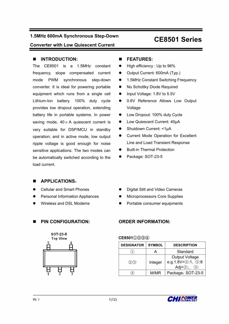
INTRODUCTION: FEATURES: The CE8501 is a 1.5MHz constant
frequency, slope compensated current
mode PWM synchronous step-down
converter. It is ideal for powering portable
equipment which runs from a single cell
Lithium-Ion battery. 100% duty cycle
provides low dropout operation, extending
battery life in portable systems. In power
saving mode, 40μA quiescent current is
very suitable for DSP/MCU in standby
operation; and in active mode, low output
ripple voltage is good enough for noise
sensitive applications. The two modes can
be automatically switched according to the
load current.
High efficiency : Up to 96%
Output Current: 600mA (Typ.) 1.5MHz Constant Switching Frequency
No Schottky Diode Required
Input Voltage: 1.8V to 5.5V
0.6V Reference Allows Low Output
Voltage
Low Dropout: 100% duty Cycle
Low Quiescent Current: 40μA
Shutdown Current: <1μA
Current Mode Operation for Excellent
Line and Load Transient Response
Built-in Thermal Protection
Package: SOT-23-5
APPLICATIONS:
Cellular and Smart Phones Personal Information Appliances Wireless and DSL Modems
Digital Still and Video Cameras Microprocessors Core Supplies Portable consumer equipments
PIN CONFIGURATION:
ORDER INFORMATION:
DESIGNATOR SYMBOL DESCRIPTION
① A Standard
②③ IntegerOutput Voltage
e.g.1.8V=②:1, ③:8Adj=②:, ③:
④ M/MR Package:SOT-23-5
1.5MHz 600mA Synchronous Step-Down
Converter with Low Quiescent Current
CE8501 Series
V0.1 2(12)
1.5MHz 600mA Synchronous Step-Down Converter with Low Quiescent Current CE8501 Series
Tabel1. Pin Description
PIN NUMBER PIN NAME FUNCTION
M MR 1 3 CE Chip Enable Pin 2 2 VSS Ground 3 5 SW External Inductor Connection Pin 4 1 VIN Power Input 5 4 VOUT/FB Output Pin/Feedback(ADJ Version)
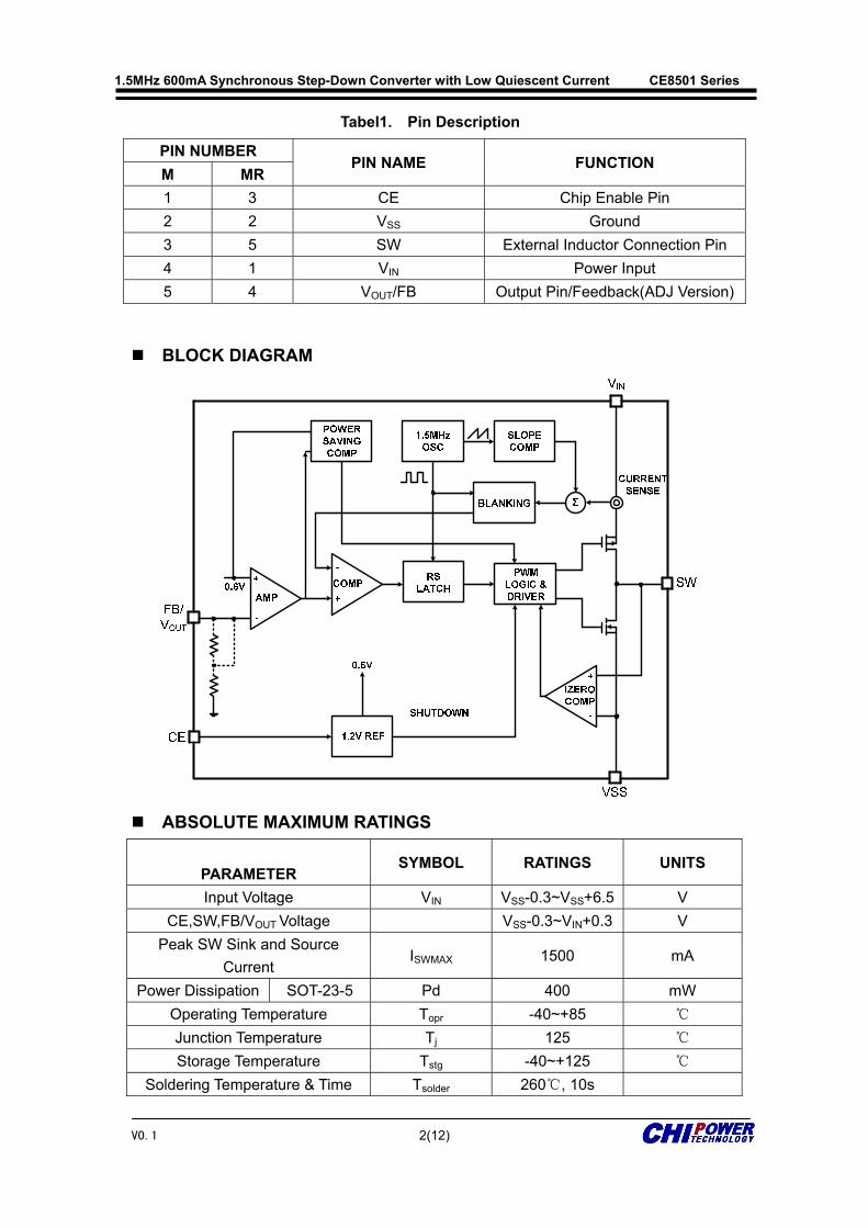
BLOCK DIAGRAM
ABSOLUTE MAXIMUM RATINGS
PARAMETER
SYMBOL RATINGS UNITS
Input Voltage VIN VSS-0.3~VSS+6.5 V CE,SW,FB/VOUT Voltage VSS-0.3~VIN+0.3 V
Peak SW Sink and Source Current
ISWMAX 1500 mA
Power Dissipation SOT-23-5 Pd 400 mW Operating Temperature Topr -40~+85 Junction Temperature Tj 125 Storage Temperature Tstg -40~+125
Soldering Temperature & Time Tsolder 260, 10s
V0.1 3(12)
1.5MHz 600mA Synchronous Step-Down Converter with Low Quiescent Current CE8501 Series
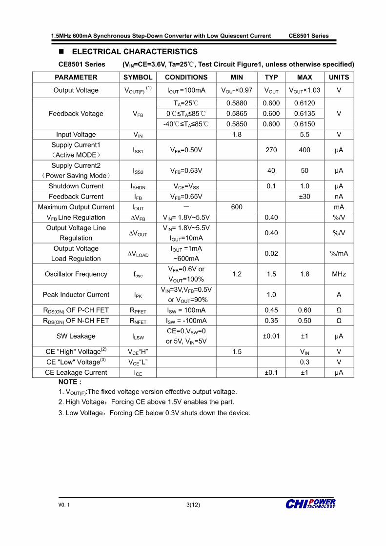
ELECTRICAL CHARACTERISTICS CE8501 Series (VIN=CE=3.6V, Ta=25, Test Circuit Figure1, unless otherwise specified)
PARAMETER SYMBOL CONDITIONS MIN TYP MAX UNITS
Output Voltage VOUT(F) (1) IOUT =100mA VOUT×0.97 VOUT VOUT×1.03 V
Feedback Voltage VFB TA=25 0.5880 0.600 0.6120
V 0≤TA≤85 0.5865 0.600 0.6135 -40≤TA≤85 0.5850 0.600 0.6150
Input Voltage VIN 1.8 5.5 V Supply Current1 (Active MODE)
ISS1 VFB=0.50V 270 400 μA
Supply Current2 (Power Saving Mode)
ISS2 VFB=0.63V 40 50 μA
Shutdown Current ISHDN VCE=VSS 0.1 1.0 μA Feedback Current IFB VFB=0.65V ±30 nA
Maximum Output Current IOUT - 600 mA VFB Line Regulation ∆VFB VIN= 1.8V~5.5V 0.40 %/V Output Voltage Line
Regulation ∆VOUT
VIN= 1.8V~5.5V IOUT=10mA
0.40 %/V
Output Voltage Load Regulation
∆VLOAD IOUT =1mA ~600mA
0.02 %/mA
Oscillator Frequency fosc VFB=0.6V or VOUT=100%
1.2 1.5 1.8 MHz
Peak Inductor Current IPK VIN=3V,VFB=0.5V
or VOUT=90% 1.0 A
RDS(ON) OF P-CH FET RPFET ISW = 100mA 0.45 0.60 Ω RDS(ON) OF N-CH FET RNFET ISW = -100mA 0.35 0.50 Ω
SW Leakage ILSW CE=0,VSW=0 or 5V, VIN=5V
±0.01 ±1 μA
CE "High" Voltage(2) VCE“H” 1.5 VIN V CE "Low" Voltage(3) VCE“L” 0.3 V CE Leakage Current ICE ±0.1 ±1 μA
NOTE : 1. VOUT(F):The fixed voltage version effective output voltage. 2. High Voltage:Forcing CE above 1.5V enables the part. 3. Low Voltage:Forcing CE below 0.3V shuts down the device.
V0.1 4(12)
1.5MHz 600mA Synchronous Step-Down Converter with Low Quiescent Current CE8501 Series
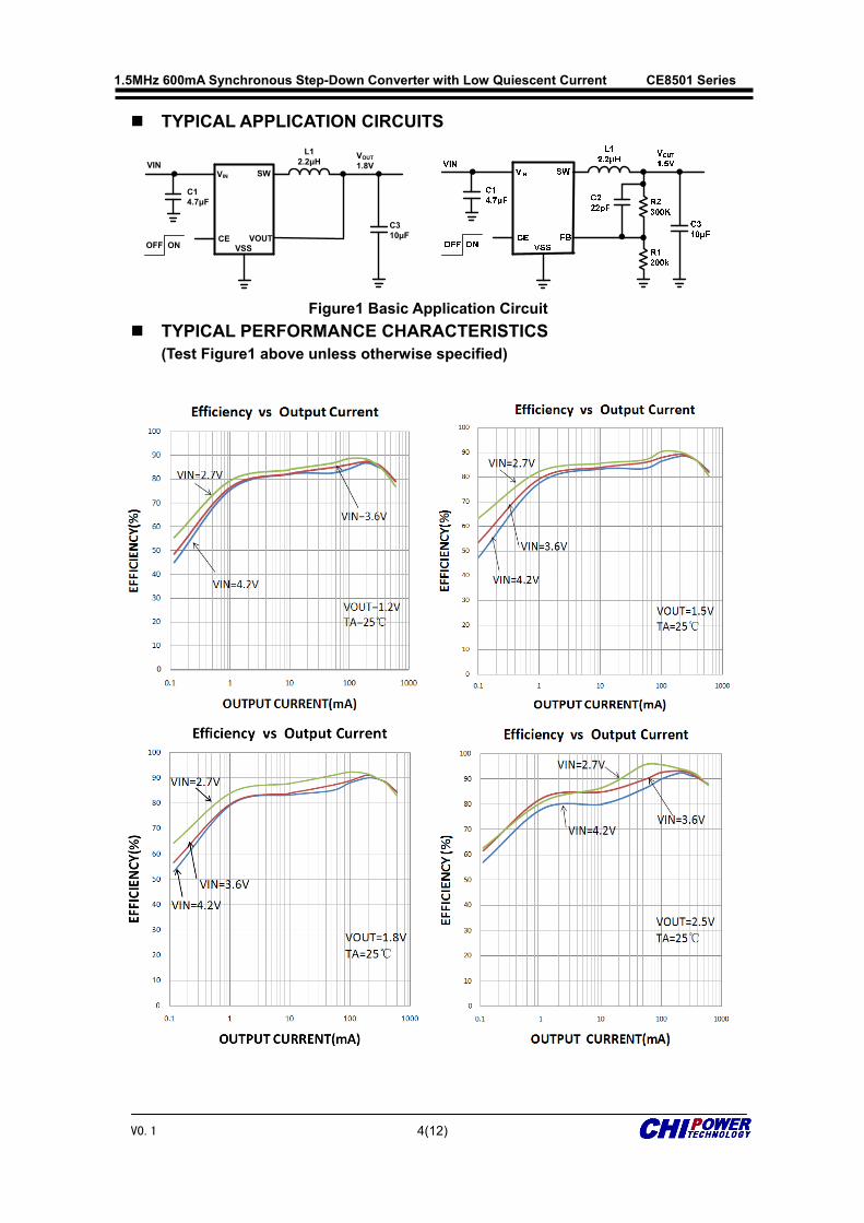
TYPICAL APPLICATION CIRCUITS
C14.7μF
L12.2μH
C310μF
VOUT1.8V
OFF ON VSSCE VOUT
SWVIN
VIN
Figure1 Basic Application Circuit
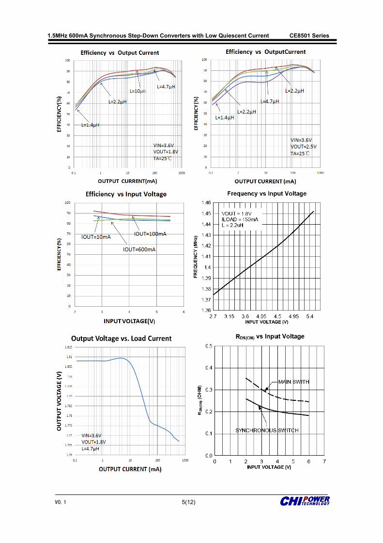
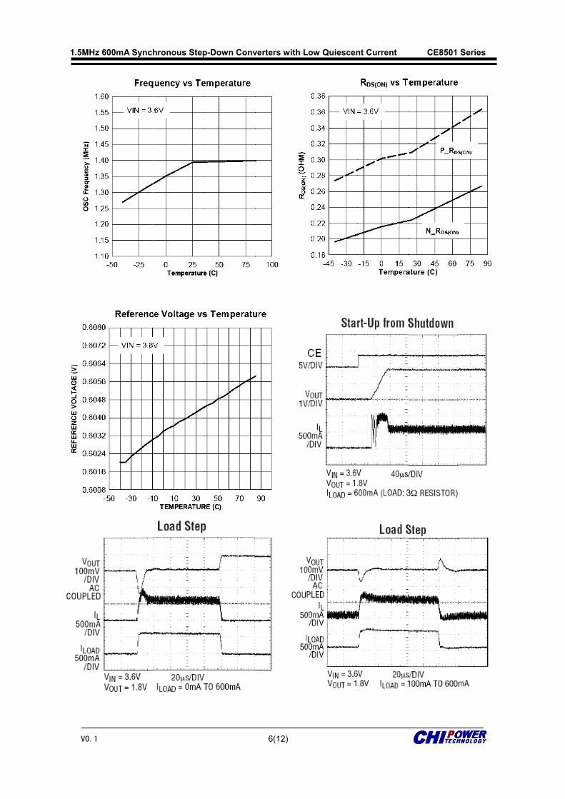
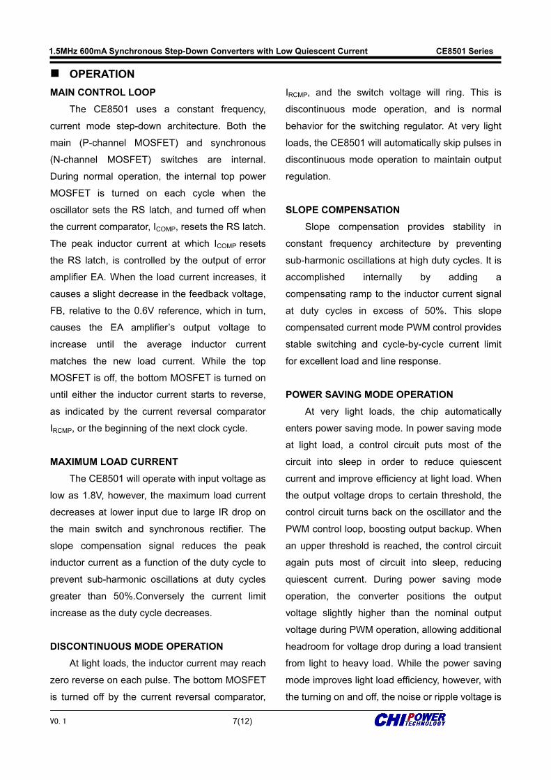
TYPICAL PERFORMANCE CHARACTERISTICS (Test Figure1 above unless otherwise specified)
V0.1
1.5MHz 6
600mA Synchhronous Stepp-Down Conv
5(12)
verters with L
Low Quiescennt Current CE8501 Series
V0.1
1.5MHz 6
600mA Synchhronous Stepp-Down Conv
6(12)
verters with L
Low Quiescennt Current CE8501 Series
V0.1 7(12)
1.5MHz 600mA Synchronous Step-Down Converters with Low Quiescent Current CE8501 Series
OPERATION MAIN CONTROL LOOP
The CE8501 uses a constant frequency,
current mode step-down architecture. Both the
main (P-channel MOSFET) and synchronous
(N-channel MOSFET) switches are internal.
During normal operation, the internal top power
MOSFET is turned on each cycle when the
oscillator sets the RS latch, and turned off when
the current comparator, ICOMP, resets the RS latch.
The peak inductor current at which ICOMP resets
the RS latch, is controlled by the output of error
amplifier EA. When the load current increases, it
causes a slight decrease in the feedback voltage,
FB, relative to the 0.6V reference, which in turn,
causes the EA amplifier’s output voltage to
increase until the average inductor current
matches the new load current. While the top
MOSFET is off, the bottom MOSFET is turned on
until either the inductor current starts to reverse,
as indicated by the current reversal comparator
IRCMP, or the beginning of the next clock cycle.
MAXIMUM LOAD CURRENT The CE8501 will operate with input voltage as
low as 1.8V, however, the maximum load current
decreases at lower input due to large IR drop on
the main switch and synchronous rectifier. The
slope compensation signal reduces the peak
inductor current as a function of the duty cycle to
prevent sub-harmonic oscillations at duty cycles
greater than 50%.Conversely the current limit
increase as the duty cycle decreases.
DISCONTINUOUS MODE OPERATION At light loads, the inductor current may reach
zero reverse on each pulse. The bottom MOSFET
is turned off by the current reversal comparator,
IRCMP, and the switch voltage will ring. This is
discontinuous mode operation, and is normal
behavior for the switching regulator. At very light
loads, the CE8501 will automatically skip pulses in
discontinuous mode operation to maintain output
regulation.
SLOPE COMPENSATION Slope compensation provides stability in
constant frequency architecture by preventing
sub-harmonic oscillations at high duty cycles. It is
accomplished internally by adding a
compensating ramp to the inductor current signal
at duty cycles in excess of 50%. This slope
compensated current mode PWM control provides
stable switching and cycle-by-cycle current limit
for excellent load and line response.
POWER SAVING MODE OPERATION At very light loads, the chip automatically
enters power saving mode. In power saving mode
at light load, a control circuit puts most of the
circuit into sleep in order to reduce quiescent
current and improve efficiency at light load. When
the output voltage drops to certain threshold, the
control circuit turns back on the oscillator and the
PWM control loop, boosting output backup. When
an upper threshold is reached, the control circuit
again puts most of circuit into sleep, reducing
quiescent current. During power saving mode
operation, the converter positions the output
voltage slightly higher than the nominal output
voltage during PWM operation, allowing additional
headroom for voltage drop during a load transient
from light to heavy load. While the power saving
mode improves light load efficiency, however, with
the turning on and off, the noise or ripple voltage is
V0.1 8(12)
1.5MHz 600mA Synchronous Step-Down Converters with Low Quiescent Current CE8501 Series
larger than that in the active Mode.
DROPOUT OPERATION As the input supply voltage decreases to a
value approaching the output voltage, the duty
cycle increases toward the maximum on-time.
Further reduction of the supply voltage forces the
main switch to remain on for more than one cycle
until reaches 100% duty cycle. The output voltage
will then be determined by the input voltage minus
the voltage drop across the P-channel MOSFET
and the inductor.
An important detail to remember is that at low
inputs supply voltages, the RDS(ON) of the
P-channel switch increases. Therefore, the user
should calculate the power dissipation when the
CE8501 is used at 100% duty cycle with low input
voltage.
APPLICATION INFORMATION The basic CE8501 application circuits are
shown in Figure 1.External component selection is
driven by the load requirement and begins with the
selection of L followed by CIN and COUT.
SETTING THE OUTPUT VOLTAGE Figure1 shows the basic application circuit
with CE8501 adjustable output version. The
external resistor sets the output voltage according
to the following equation:
VOUT 0.6V 1R2R1
Table 2.Resistor select for output voltage setting
VOUT R1 R2 1.2V 316K 316K 1.5V 316K 470K 1.8V 316K 634K 2.5V 316K 1M
INPUT CAPACITOR SELECTION
In continuous mode, the source current of the
top MOSFET is a square wave of duty cycle
VOUT/VIN. To prevent large voltage transients, a
low ESR input capacitor sized for the maximum
RMS current must be used. The maximum RMS
capacitor current is given by:
CIN required IRMS IOMAXVOUT VIN VOUT
/
VIN
This formula has a maximum at VIN = 2VOUT,
where IRMS = IOUT/2. This simple worst-case
condition is commonly used for design because
even significant deviations do not offer much relief.
Ceramic capacitors with X5R or X7R dielectrics
are highly recommended because of their low
ESR and small temperature coefficients. A 4.7μF
ceramic capacitor for most application is sufficient.
INDUCTOR SELECTION
For most applications, the value of the
inductor will fall in the range of 1μH to 4.7μH. Its
value is chosen based on the desired ripple
current. Large value inductor lower ripple current
and small value inductor result in higher ripple
currents. Higher VIN or VOUT also increases the
ripple current as shown in the following equation:
∆ILVOUT VIN VOUT
VIN L f
A reasonable starting point for setting ripple
current is I L=240mA (40% of 600mA). The DC
current rating of the inductor should be at least
equal to the maximum load current plus half the
ripple current to prevent core saturation.
Different core materials and shapes will
change the size/current and price/current
relationship of an inductor. The choice of which
V0.1 9(12)
1.5MHz 600mA Synchronous Step-Down Converters with Low Quiescent Current CE8501 Series
style inductor to use often depends more on the
price vs. size requirements and any radiated
field/EMI requirements than on what the CE8501
requires to operate. Table 3 shows some typical
surface mount inductors that work well in CE8501
applications.
Table 3.Representative Surface Mount Inductors PART
NUMBER VALUE
(μH) MAX DCR (mΩ)
MAX DC CURRENT
(A)
SIZE W×L×H
(mm3)
SumidaCDRH 3D16
2.2 3.3 4.7
75 110 162
1.20 1.10 0.90
3.8×3.8×1.8
SumidaCR43
2.2 3.3 4.7
71.2 86.2 108.7
1.75 1.44 1.15
4.5×4.0×3.5
SumidaCDRH 4D18
2.2 3.3 4.7
75 110 162
1.32 1.04 0.84
4.7×4.7×2.0
OUTPUT CAPACITOR SELECTION The selection of COUT is driven by the
required effective series resistance (ESR).
Typically, once the ESR requirement for COUT has
been met, the RMS current rating generally far
exceeds the IRIPPLE requirement. The output ripple
VOUT is determined by:
∆VOUT ∆IL ESR1
8fCOUT
Where f = operating frequency, COUT = output
capacitance and I L = ripple current in the
inductor. For a fixed output voltage, the output
ripple is highest at maximum input voltage since
I L increase with input voltage. Ceramic
capacitors with X5R or X7R dielectrics are
recommended due to their low ESR and high
ripple current.
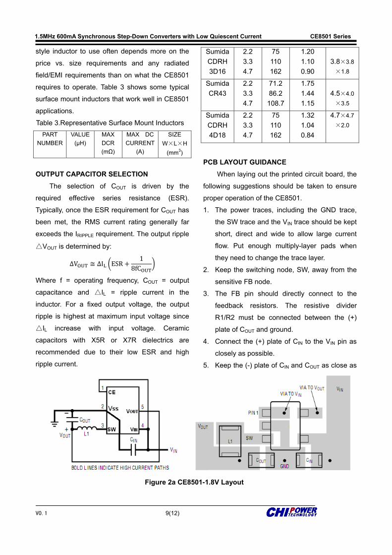
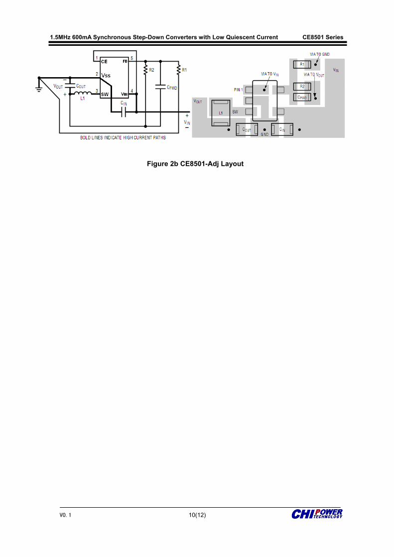
PCB LAYOUT GUIDANCE When laying out the printed circuit board, the
following suggestions should be taken to ensure
proper operation of the CE8501.
1. The power traces, including the GND trace,
the SW trace and the VIN trace should be kept
short, direct and wide to allow large current
flow. Put enough multiply-layer pads when
they need to change the trace layer.
2. Keep the switching node, SW, away from the
sensitive FB node.
3. The FB pin should directly connect to the
feedback resistors. The resistive divider
R1/R2 must be connected between the (+)
plate of COUT and ground.
4. Connect the (+) plate of CIN to the VIN pin as
closely as possible.
5. Keep the (-) plate of CIN and COUT as close as
possible.
Figure 2a CE8501-1.8V Layout
V0.1 10(12)
1.5MHz 600mA Synchronous Step-Down Converters with Low Quiescent Current CE8501 Series
Figure 2b CE8501-Adj Layout
V0.1
1.5MHz
600mA Sync
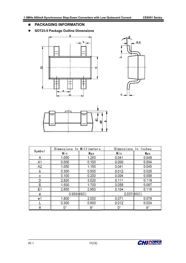
PACKAGSOT23-5 P
chronous Ste
GING INFOPackage Ou
p-Down Conv
RMATIONutline Dimen
11(12)
verters with L
N
nsions
Low Quiescent Current CE8501 Series
V0.1 12(12)
1.5MHz 600mA Synchronous Step-Down Converters with Low Quiescent Current CE8501 Series
© Nanjing Chipower Electronics Inc.
Chipower cannot assume responsibility for use of any circuitry other than circuitry entirely embodied in a
Chipower product. No circuit patent license, copyrights or other intellectual property rights are implied.
Chipower reserves the right to make changes to their products or specifications without notice.
Customers are advised to obtain the latest version of relevant information to verify, before placing orders,
that information being relied on is current and complete.