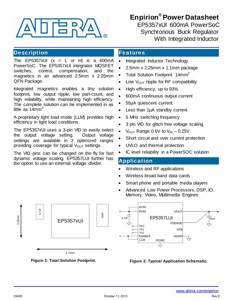
Enpirion ® Power Datasheet EP5357xUI 600mA PowerSoC Synchronous Buck Regulator With Integrated Inductor Description The EP5357xUI (x = L or H) is a 600mA PowerSoC. The EP5357xUI integrates MOSFET switches, control, compensation, and the magnetics in an advanced 2.5mm x 2.25mm QFN Package. Integrated magnetics enables a tiny solution footprint, low output ripple, low part-count, and high reliability, while maintaining high efficiency. The complete solution can be implemented in as little as 14mm 2 . A proprietary light load mode (LLM) provides high efficiency in light load conditions. The EP5357xUI uses a 3-pin VID to easily select the output voltage setting. Output voltage settings are available in 2 optimized ranges providing coverage for typical V OUT settings. The VID pins can be changed on the fly for fast dynamic voltage scaling. EP5357LUI further has the option to use an external voltage divider. EP5357xUI 4.7uF 10uF 4.75mm 2.25mm Figure 1: Total Solution Footprint. Features • Integrated Inductor Technology • 2.5mm x 2.25mm x 1.1mm package • Total Solution Footprint 14mm 2 • Low V OUT ripple for RF compatibility • High efficiency, up to 93% • 600mA continuous output current • 55μA quiescent current • Less than 1μA standby current • 5 MHz switching frequency • 3 pin VID for glitch free voltage scaling • V OUT Range 0.6V to V IN – 0.25V • Short circuit and over current protection • UVLO and thermal protection • IC level reliability in a PowerSOC solution Application • Wireless and RF applications • Wireless broad band data cards • Smart phone and portable media players • Advanced Low Power Processors, DSP, IO, Memory, Video, Multimedia Engines AVIN PVIN ENABLE VSENSE VOUT AGND PGND 10uF 4.7uF EP5357LUI VS2 VS1 VSO VFB LLM Figure 2: Typical Application Schematic. www.altera.com/enpirion 03409 October 11, 2013 Rev E

Welcome message from author
This document is posted to help you gain knowledge. Please leave a comment to let me know what you think about it! Share it to your friends and learn new things together.
Transcript
Enpirion® Power Datasheet EP5357xUI 600mA PowerSoC
Synchronous Buck Regulator With Integrated Inductor
Description The EP5357xUI (x = L or H) is a 600mA PowerSoC. The EP5357xUI integrates MOSFET switches, control, compensation, and the magnetics in an advanced 2.5mm x 2.25mm QFN Package.
Integrated magnetics enables a tiny solution footprint, low output ripple, low part-count, and high reliability, while maintaining high efficiency. The complete solution can be implemented in as little as 14mm2.
A proprietary light load mode (LLM) provides high efficiency in light load conditions.
The EP5357xUI uses a 3-pin VID to easily select the output voltage setting. Output voltage settings are available in 2 optimized ranges providing coverage for typical VOUT settings.
The VID pins can be changed on the fly for fast dynamic voltage scaling. EP5357LUI further has the option to use an external voltage divider.
EP5357xUI
4.7u
F
10uF
4.75mm
2.25
mm
Figure 1: Total Solution Footprint.
Features • Integrated Inductor Technology • 2.5mm x 2.25mm x 1.1mm package • Total Solution Footprint 14mm2 • Low VOUT ripple for RF compatibility • High efficiency, up to 93% • 600mA continuous output current • 55µA quiescent current • Less than 1µA standby current • 5 MHz switching frequency • 3 pin VID for glitch free voltage scaling • VOUT Range 0.6V to VIN – 0.25V • Short circuit and over current protection • UVLO and thermal protection • IC level reliability in a PowerSOC solution
Application • Wireless and RF applications • Wireless broad band data cards • Smart phone and portable media players • Advanced Low Power Processors, DSP, IO,
Memory, Video, Multimedia Engines
AVINPVIN
ENABLE
VSENSE
VOUT
AGNDPGND
10uF4.7uF EP5357LUI
VS2VS1VSO
VFB
LLM
Figure 2: Typical Application Schematic.
www.altera.com/enpirion 03409 October 11, 2013 Rev E

EP5357LUI/EP5357HUI
Ordering Information Part Number Comment Package
EP5357LUI LOW VID Range 16-pin QFN T&R
EP5357HUI HIGH VID Range 16-pin QFN T&R
EVB-EP5357LUI EP5357LUI Evaluation Board
EVB-EP5357HUI EP5357HUI Evaluation Board
Pin Assignments (Top View)
Figure 3: EP5357LUI Pin Out Diagram (Top View)
Figure 4: EP5357HUI Pin Out Diagram (Top View)
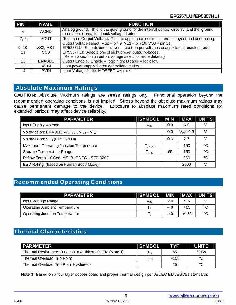
Pin Description
PIN NAME FUNCTION
1, 15, 16 NC(SW)
NO CONNECT – These pins are internally connected to the common switching node of the internal MOSFETs. NC (SW) pins are not to be electrically connected to any external signal, ground, or voltage. However, they must be soldered to the PCB. Failure to follow this guideline may result in part malfunction or damage to the device.
2 PGND Power ground. Connect this pin to the ground electrode of the Input and output filter capacitors.
3 LLM LLM (Light Load Mode – “LLM”) pin. Logic-High enables automatic LLM/PWM and logic-low places the device in fixed PWM operation. LLM pin should be connected to ENABLE, or should be disabled before ENABLE is pulled low.
4 VFB/NC EP5357LUI: Feed back pin for external divider option. EP5357HUI: No Connect
5 VSENSE Sense pin for preset output voltages. Refer to application section for proper configuration.
PVIN
AVIN
ENABLE
VS0
VS1
VS2
NC(SW)
PGND
LLM
VFB
VSENSE
AGND
VO
UT
VO
UT
NC
(SW
)
NC
(SW
)EP
5357
LUI
3
1
4
2
6
5
16 15
7 8
12
11
13
10
9
14
PVIN
AVIN
ENABLE
VS0
VS1
VS2
NC(SW)
PGND
LLM
NC
VSENSE
AGND
VO
UT
VO
UT
NC
(SW
)
NC
(SW
)EP
5357
HU
I
3
1
4
2
6
5
16 15
7 8
12
11
13
10
9
14
2 www.altera.com/enpirion 03409 October 11, 2013 Rev E
EP5357LUI/EP5357HUI
PIN NAME FUNCTION 6 AGND Analog ground. This is the quiet ground for the internal control circuitry, and the ground
return for external feedback voltage divider 7, 8 VOUT Regulated Output Voltage. Refer to application section for proper layout and decoupling.
9, 10, 11
VS2, VS1, VS0
Output voltage select. VS2 = pin 9, VS1 = pin 10, VS0 = pin 11. EP5357LUI: Selects one of seven preset output voltages or an external resistor divider. EP5357HUI: Selects one of eight preset output voltages. (Refer to section on output voltage select for more details.)
12 ENABLE Output Enable. Enable = logic high; Disable = logic low 13 AVIN Input power supply for the controller circuitry. 14 PVIN Input Voltage for the MOSFET switches.
Absolute Maximum Ratings CAUTION: Absolute Maximum ratings are stress ratings only. Functional operation beyond the recommended operating conditions is not implied. Stress beyond the absolute maximum ratings may cause permanent damage to the device. Exposure to absolute maximum rated conditions for extended periods may affect device reliability.
PARAMETER SYMBOL MIN MAX UNITS Input Supply Voltage VIN -0.3 6.0 V
Voltages on: ENABLE, VSENSE, VSO – VS2 -0.3 VIN+ 0.3 V
Voltages on: VFB (EP5357LUI) -0.3 2.7 V
Maximum Operating Junction Temperature TJ-ABS 150 °C Storage Temperature Range TSTG -65 150 °C Reflow Temp, 10 Sec, MSL3 JEDEC J-STD-020C 260 °C ESD Rating (based on Human Body Mode) 2000 V
Recommended Operating Conditions
PARAMETER SYMBOL MIN MAX UNITS Input Voltage Range VIN 2.4 5.5 V Operating Ambient Temperature TA -40 +85 °C Operating Junction Temperature TJ -40 +125 °C
Thermal Characteristics
PARAMETER SYMBOL TYP UNITS Thermal Resistance: Junction to Ambient –0 LFM (Note 1) θJA 85 °C/W Thermal Overload Trip Point TJ-TP +155 °C Thermal Overload Trip Point Hysteresis 25 °C
Note 1: Based on a four layer copper board and proper thermal design per JEDEC EIJ/JESD51 standards
3 www.altera.com/enpirion 03409 October 11, 2013 Rev E
EP5357LUI/EP5357HUI
Electrical Characteristics NOTE: TA = -40°C to +85°C unless otherwise noted. Typical values are at TA = 25°C, VIN = 3.6V. CIN = 4.7µF MLCC, COUT = 10µF MLCC
PARAMETER SYMBOL TEST CONDITIONS MIN TYP MAX UNITS Operating Input Voltage Range VIN 2.4 5.5 V
Under Voltage Lock-out – VIN Rising VUVLO_R 2.0 V
Under Voltage Lock-out – VIN Falling VUVLO_F 1.9 V
Drop Out Resistance RDO Input to Output Resistance 350 500 mΩ
Output Voltage Range VOUT EP5357LUI (VDO = ILOAD X RDO) EP5357HUI
0.6 1.8 VIN-VDO
3.3 V
Dynamic Voltage Slew Rate VSLEW
EP5357LUI (VID MODE) EP5357HUI (VID MODE) 4
8 V/mS
VID Preset VOUT Initial Accuracy ∆VOUT
TA = 25°C, VIN = 3.6V; ILOAD = 100mA ; 0.8V ≤ VOUT ≤ 3.3V
-2 +2 %
Line Regulation ∆VOUT_LINE 2.4V ≤ VIN ≤ 5.5V 0.03 %/V Load Regulation ∆VOUT_LOAD 0A ≤ ILOAD ≤ 600mA 0.48 %/A
Temperature Variation ∆VOUT_TEMPL -40°C ≤ TA ≤ +85°C 24 ppm/°C Output Current IOUT 600 mA Shut-down Current ISD Enable = Low 0.75 µA EP5357HUI Operating Quiescent Current IQ ILOAD=0; Preset Output Voltages,
LLM=High 55 µA
EP5357LUI Operating Quiescent Current IQ ILOAD=0; Preset Output Voltages,
LLM=High 65 µA
OCP Threshold ILIM 2.4V ≤ VIN ≤ 5.5V 0.6V ≤ VOUT ≤ 3.3V 1.4 A
Feedback Pin Voltage Initial Accuracy VFB
TA = 25°C, VIN = 3.6V; ILOAD = 100mA ; 0.8V ≤ VOUT ≤ 3.3V
.588 0.6 0.612 V
Feedback Pin Voltage variation over Line, Load, and Temperature
VFB -40°C ≤ TA ≤ +85°C; 2.4V ≤ VIN ≤ 5.5V 0mA ≤ ILOAD ≤ 600mA
.582 0.6 0.618. V
Feedback Pin Input Current IFB Note 1 <100 nA
VS0-VS2, Pin Logic Low VVSLO 0.0 0.3 V
VS0-VS2, Pin Logic High VVSHI 1.4 VIN V
VS0-VS2, Pin Input Current IVSX Note 1 <100 nA
Enable Pin Logic Low VENLO 0.3 V Enable Pin Logic High VENHI 1.4 V Enable Pin Current IENABLE Note 1 <100 nA
4 www.altera.com/enpirion 03409 October 11, 2013 Rev E

EP5357LUI/EP5357HUI
PARAMETER SYMBOL TEST CONDITIONS MIN TYP MAX UNITS
LLM Engage Headroom Minimum VIN-VOUT to ensure proper LLM operation 600 mV
LLM Pin Logic Low VLLMLO 0.3 V LLM Pin Logic High VLLMHI 1.4 V LLM Pin Current ILLM <100 nA Operating Frequency FOSC 5 MHz Soft Start Operation
Soft Start Slew Rate ∆VSS EP5357HUI (VID MODE) EP5357LUI (VID MODE)
8 4 V/mS
VOUT Rise Time TRISE Time to 90% VOUT (VFB MODE) 180 250 uSec
Note 1: Parameter guaranteed by design
Typical Performance Characteristics
Efficiency vs. Load Current: VIN = 5.0V, VOUT (from
top to bottom) = 3.3, 2.5, 1.8, 1.2V
Efficiency vs. Load Current: VIN = 3.7V, VOUT (from
top to bottom) = 2.5, 1.8, 1.2V
Efficiency vs. Load Current: VIN = 3.3V, VOUT (from
top to bottom) = 2.5, 1.8, 1.2V
4550556065707580859095
10 100 1000Load Current (mA)
Effic
ienc
y (%
)
4550556065707580859095
10 100 1000Load Current (mA)
Effic
ienc
y (%
)
4550556065707580859095
10 100 1000Load Current (mA)
Effic
ienc
y (%
)
LLM LLM
PWM PWM
LLM
PWM
5 www.altera.com/enpirion 03409 October 11, 2013 Rev E

EP5357LUI/EP5357HUI
Start Up Waveform: VIN = 5.0V, VOUT = 3.3V;
ILOAD = 10mA (VID MODE)
Start Up Waveform: VIN = 5.0V, VOUT = 3.3V;
ILOAD = 1000mA (VID MODE)
Shut-down Waveform: VIN = 5.0V, VOUT = 3.3V;
ILOAD = 10mA, PWM
Shut-down Waveform: VIN = 5.0V, VOUT = 3.3V;
ILOAD = 500mA, PWM
Output Ripple: VIN = 5.0V, VOUT = 1.2V, Load = 10mA
LLM enabled
Output Ripple: VIN = 5.0V, VOUT = 1.2V, Load = 500mA
50mV/Div 5mV/Div
6 www.altera.com/enpirion 03409 October 11, 2013 Rev E

EP5357LUI/EP5357HUI
Output Ripple: VIN = 5.0V, VOUT = 3.3V, Load = 10mA
LLM enabled
Output Ripple: VIN = 5.0V, VOUT = 3.3V,
Load = 500mA
Output Ripple: VIN = 3.3V, VOUT = 1.8V, Load = 10mA
LLM enabled
Output Ripple: VIN = 3.3V, VOUT = 1.8V
Load = 500mA
Output Ripple: VIN = 3.3V, VOUT = 1.2V, Load = 10mA
LLM enabled
Output Ripple: VIN = 3.3V, VOUT = 1.2V,
Load = 500mA
5mV/Div 50mV/Div
5mV/Div 50mV/Div
50mV/Div 5mV/Div
7 www.altera.com/enpirion 03409 October 11, 2013 Rev E
EP5357LUI/EP5357HUI
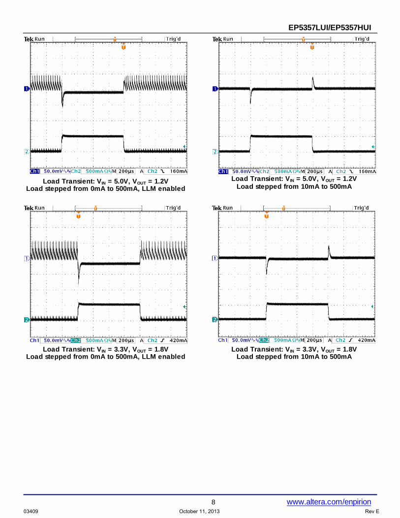
Load Transient: VIN = 5.0V, VOUT = 1.2V
Load stepped from 0mA to 500mA, LLM enabled
Load Transient: VIN = 5.0V, VOUT = 1.2V
Load stepped from 10mA to 500mA
Load Transient: VIN = 3.3V, VOUT = 1.8V
Load stepped from 0mA to 500mA, LLM enabled
Load Transient: VIN = 3.3V, VOUT = 1.8V
Load stepped from 10mA to 500mA
8 www.altera.com/enpirion 03409 October 11, 2013 Rev E

EP5357LUI/EP5357HUI
Functional Block Diagram
Figure 5: Functional Block Diagram
DAC
Switch
VREF
(+)
(-)Error Amp
VSENSE
VFB
VOUT
Package Boundry
P-Drive
N-Drive
UVLO
Thermal Limit
Current Limit
Soft Start
SawtoothGenerator
(+)
(-)PWM Comp
PVIN
ENABLE
PGND
Logic
CompensationNetwork
NC(SW)
Voltage Select
VS0 VS1AVIN VS2AGND
Mode Logic
LLM
9 www.altera.com/enpirion 03409 October 11, 2013 Rev E

EP5357LUI/EP5357HUI
Detailed Description Functional Overview The EP5357xUI requires only 2 small MLCC capacitors for a complete DC-DC converter solution. The device integrates MOSFET switches, PWM controller, Gate-drive, compensation, and inductor into a tiny 2.5mm x 2.25mm x 1.1mm QFN package. Advanced package design, along with the high level of integration, provides very low output ripple and noise. The EP5357xUI uses voltage mode control for high noise immunity and load matching to advanced ≤90nm loads. A 3-pin VID allows the user to choose from one of 8 output voltage settings. The EP5357xUI comes with two VID output voltage ranges. The EP5357HUI provides VOUT settings from 1.8V to 3.3V, the EP5357LUI provides VID settings from 0.8V to 1.5V, and also has an external resistor divider option to program output setting over the 0.6V to VIN-0.25V range. The EP5357xUI provides the industry’s highest power density of any 600mA DCDC converter solution. The key enabler of this revolutionary integration is Altera Enpirion’s proprietary power MOSFET technology. The advanced MOSFET switches are implemented in deep-submicron CMOS to supply very low switching loss at high switching frequencies and to allow a high level of integration. The semiconductor process allows seem-less integration of all switching, control, and compensation circuitry. The proprietary magnetics design provides high-density/high-value magnetics in a very small footprint. Altera Enpirion magnetics are carefully matched to the control and compensation circuitry yielding an optimal solution with assured performance over the entire operating range. Protection features include under-voltage lock-out (UVLO), over-current protection (OCP), short circuit protection, and thermal overload protection.
Integrated Inductor The EP5357xUI utilizes a proprietary low loss integrated inductor. The integration of the inductor greatly simplifies the power supply design process. The inherent shielding and compact construction of the integrated inductor reduces the conducted and radiated noise that can couple into the traces of the printed circuit board. Further, the package layout is optimized to reduce the electrical path length for the high di/dT input AC ripple currents that are a major source of radiated emissions from DC-DC converters. The integrated inductor provides the optimal solution to the complexity, output ripple, and noise that plague low power DCDC converter design.
Voltage Mode Control The EP5357xUI utilizes an integrated type III compensation network. Voltage mode control is inherently impedance matched to the sub 90nm process technology that is used in today’s advanced ICs. Voltage mode control also provides a high degree of noise immunity at light load currents so that low ripple and high accuracy are maintained over the entire load range. The very high switching frequency allows for a very wide control loop bandwidth and hence excellent transient performance.
Light Load Mode (LLM) Operation The EP5357xUI uses a proprietary light load mode to provide high efficiency in the low load operating condition. When the LLM pin is high, the device is in automatic LLM/PWM mode. When the LLM pin is low, the device is in PWM mode. In automatic LLM/PWM mode, when a light load condition is detected, the device will (1) step VOUT up by approximately 1.5% above the nominal operating output voltage setting, VNOM, and then (2) shut down unnecessary circuitry, and (3) monitor VOUT. When VOUT falls below VNOM, the device will repeat (1), (2), and (3). The voltage step up, or pre-positioning, improves transient droop when a load transient causes a transition from LLM mode to PWM mode. If a load transient occurs, causing VOUT to fall below the threshold VMIN, the device will
10 www.altera.com/enpirion 03409 October 11, 2013 Rev E

EP5357LUI/EP5357HUI
exit LLM operation and begin normal PWM operation. Figure 6 demonstrates VOUT behavior during transition into and out of LLM operation.
Figure 6: VOUT Behavior in LLM Operation
Figure 7: VOUT Droop during Periodic LLM Exit
Many multi-mode DCDC converters suffer from a condition that occurs when the load current increases only slowly so that there is no load transient driving VOUT below the VMIN threshold. In this condition, the device would never exit LLM operation. This could adversely affect efficiency and cause unwanted ripple. To prevent this from occurring, the EP5357xUI periodically exits LLM mode into PWM mode and measures the load current. If the load current is above the LLM threshold current, the device will remain in PWM mode. If the load current is below the LLM threshold, the device will re-enter LLM operation. There will be a small droop in VOUT at the point where the device exits and re-enters LLM, as shown in Figure 7.
Figure 8: Typical load current for LLM engage and disengage versus VOUT for selected input voltages
Table 1: Load current below which the device can be certain to be in LLM operation. These values are
guaranteed by design
The load current at which the device will enter LLM mode is a function of input and output voltage. Figure 8 shows the typical value at which the device will enter LLM operation. The actual load current at which the device will enter LLM operation can vary by +/-30%. Table 1 shows the minimum load current below which the device is guaranteed to be in LLM operating mode. To ensure normal LLM operation, LLM mode should be enabled/disabled with specific sequencing. For applications with explicit LLM pin control, enable LLM after VIN ramp up is complete; disable LLM before VIN ramp
VOUT
IOUT
LLM Ripple
PWM Ripple
VMAX
VNOM
VMIN
Load Step
LLM Threshold Current vs. VOUT
0
50
100
150
200
250
0.8 1.1 1.4 1.7 2.0 2.3 2.6 2.9 3.2
VOUT (V)
LLM
Thr
esho
ld (m
A)
VIN=5V (top curve)
VIN=4.2V
VIN=3.7V
VIN=3.3V (bottom curve)
3.3 3.7 4.3 5.03.30 105 1473.00 62 122 1562.90 89 126 1582.60 56 106 136 1622.50 69 111 138 1622.20 101 120 141 1602.10 105 122 141 1581.80 111 124 138 1501.50 111 120 130 1381.45 111 119 128 1361.20 105 111 117 1221.15 103 108 114 1191.10 101 106 111 1161.05 99 104 108 1130.80 87 89 92 94
VINVOUT
Device exits LLM, tests load current
11 www.altera.com/enpirion 03409 October 11, 2013 Rev E

EP5357LUI/EP5357HUI
down. For applications with ENABLE control, tie LLM to ENABLE; enable device after VIN ramp up is complete and disable device before VIN ramp down begins. For devices with ENABLE and LLM tied to VIN, contact Power Applications support for specific recommendations Increased output filter capacitance and/or increased bulk capacitance at the load will decrease the magnitude of the LLM ripple. Refer to the section on output filter capacitance for maximum values of output filter capacitance and the Soft-Start section for maximum bulk capacitance at the load. NOTE: For proper LLM operation the EP5357xUI requires a minimum difference between VIN and VOUT of 600mV. If this condition is not met, the device cannot be assured proper LLM operation. NOTE: Automatic LLM/PWM is not available when using the external resistor divider option for VOUT programming. Soft Start Internal soft start circuits limit in-rush current when the device starts up from a power down condition or when the “ENABLE” pin is asserted “high”. Digital control circuitry limits the VOUT ramp rate to levels that are safe for the Power MOSFETS and the integrated inductor. The EP5357HUI has a soft-start slew rate that is twice that of the EP5357LUI. When the EP5357LUI is configured in external resistor divider mode, the device has a fixed VOUT ramp time. Therefore, the ramp rate will vary with the output voltage setting. Output voltage ramp time is given in the Electrical Characteristics Table. Excess bulk capacitance on the output of the device can cause an over-current condition at startup. The maximum total capacitance on the output, including the output filter capacitor and bulk and decoupling capacitance, at the load, is given as: EP5357LUI: COUT_TOTAL_MAX = COUT_Filter + COUT_BULK = 200uF
EP5357HUI: COUT_TOTAL_MAX = COUT_Filter + COUT_BULK = 100uF EP5357LUI in external divider mode: COUT_TOTAL_MAX = 2.25x10⁻⁴/VOUT Farads The nominal value for COUT is 10uF. See the applications section for more details. Over Current/Short Circuit Protection The current limit function is achieved by sensing the current flowing through a sense P-MOSFET which is compared to a reference current. When this level is exceeded the P-FET is turned off and the N-FET is turned on, pulling VOUT low. This condition is maintained for approximately 0.5mS and then a normal soft start is initiated. If the over current condition still persists, this cycle will repeat. Under Voltage Lockout During initial power up an under voltage lockout circuit will hold-off the switching circuitry until the input voltage reaches a sufficient level to insure proper operation. If the voltage drops below the UVLO threshold the lockout circuitry will again disable the switching. Hysteresis is included to prevent chattering between states.
Enable The ENABLE pin provides a means to shut down the converter or enable normal operation. A logic low will disable the converter and cause it to shut down. A logic high will enable the converter into normal operation. NOTE: The ENABLE pin must not be left floating.
Thermal Shutdown When excessive power is dissipated in the chip, the junction temperature rises. Once the junction temperature exceeds the thermal shutdown temperature the thermal shutdown circuit turns off the converter output voltage thus allowing the device to cool. When the junction temperature decreases by 15C°, the device will go through the normal startup process.
12 www.altera.com/enpirion 03409 October 11, 2013 Rev E
EP5357LUI/EP5357HUI
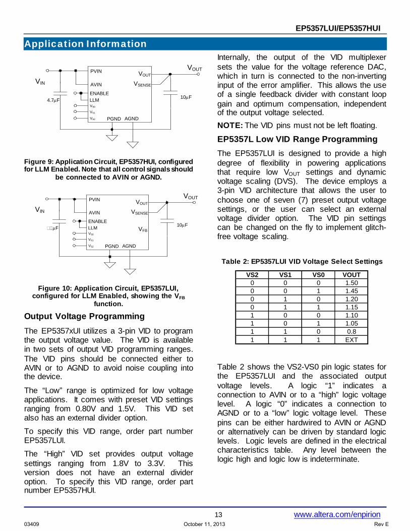
Application Information
VIN VSENSE
PVIN
VS1
VS2
VS0
10µF4.7µF
VOUTVOUT
AGND
ENABLE
PGND
AVIN
LLM
Figure 9: Application Circuit, EP5357HUI, configured for LLM Enabled. Note that all control signals should
be connected to AVIN or AGND.
VIN VSENSE
PVIN
VS1
VS2
VS0
10µFµF
VOUTVOUT
AGND
ENABLE
VFB
PGND
AVIN
LLM
Figure 10: Application Circuit, EP5357LUI, configured for LLM Enabled, showing the VFB
function. Output Voltage Programming The EP5357xUI utilizes a 3-pin VID to program the output voltage value. The VID is available in two sets of output VID programming ranges. The VID pins should be connected either to AVIN or to AGND to avoid noise coupling into the device.
The “Low” range is optimized for low voltage applications. It comes with preset VID settings ranging from 0.80V and 1.5V. This VID set also has an external divider option.
To specify this VID range, order part number EP5357LUI.
The “High” VID set provides output voltage settings ranging from 1.8V to 3.3V. This version does not have an external divider option. To specify this VID range, order part number EP5357HUI.
Internally, the output of the VID multiplexer sets the value for the voltage reference DAC, which in turn is connected to the non-inverting input of the error amplifier. This allows the use of a single feedback divider with constant loop gain and optimum compensation, independent of the output voltage selected. NOTE: The VID pins must not be left floating.
EP5357L Low VID Range Programming The EP5357LUI is designed to provide a high degree of flexibility in powering applications that require low VOUT settings and dynamic voltage scaling (DVS). The device employs a 3-pin VID architecture that allows the user to choose one of seven (7) preset output voltage settings, or the user can select an external voltage divider option. The VID pin settings can be changed on the fly to implement glitch-free voltage scaling.
Table 2: EP5357LUI VID Voltage Select Settings
Table 2 shows the VS2-VS0 pin logic states for the EP5357LUI and the associated output voltage levels. A logic “1” indicates a connection to AVIN or to a “high” logic voltage level. A logic “0” indicates a connection to AGND or to a “low” logic voltage level. These pins can be either hardwired to AVIN or AGND or alternatively can be driven by standard logic levels. Logic levels are defined in the electrical characteristics table. Any level between the logic high and logic low is indeterminate.
VS2 VS1 VS0 VOUT0 0 0 1.500 0 1 1.450 1 0 1.200 1 1 1.151 0 0 1.101 0 1 1.051 1 0 0.81 1 1 EXT
13 www.altera.com/enpirion 03409 October 11, 2013 Rev E

EP5357LUI/EP5357HUI
EP5357LUI External Voltage Divider The external divider option is chosen by connecting VID pins VS2-VS0 to VIN or a logic “1” or “high”. The EP5357LUI uses a separate feedback pin, VFB, when using the external divider. VSENSE must be connected to VOUT as indicated in Figure 11. The output voltage is selected by the following formula:
( )RbRa
OUT VV += 16.0
Ra must be chosen as 237KΩ to maintain loop gain. Then Rb is given as:
Ω−
=6.0
102.142 3
OUTb V
xR
VOUT can be programmed over the range of 0.6V to (VIN – 0.25V).
NOTE: Dynamic Voltage Scaling is not allowed between internal preset voltages and external divider.
NOTE: LLM is not functional when using the external divider option. Tie the LLM pin to AGND.
VINVSense
VS0
VS2
EP5357L
10µF4.7uF
VOUT
VOUT
AGND
ENABLE Ra
Rb
VFB
VS1
PGND
AVIN
PVIN
Figure 11: EP5357LUI using external divider
EP5357HUI High VID Range Programming The EP5357HUI VOUT settings are optimized for higher nominal voltages such as those required to power IO, RF, or IC memory. The preset voltages range from 1.8V to 3.3V. There are eight (8) preset output voltage settings. The EP5357HUI does not have an external divider option. As with the EP5357LUI, the VID pin settings can be changed while the device is enabled.
Table 3 shows the VS0-VS2 pin logic states for the EP5357HUI and the associated output voltage levels. A logic “1” indicates a
connection to AVIN or to a “high” logic voltage level. A logic “0” indicates a connection to AGND or to a “low” logic voltage level. These pins can be either hardwired to AVIN or AGND or alternatively can be driven by standard logic levels. Logic levels are defined in the electrical characteristics table. Any level between the logic high and logic low is indeterminate. These pins must not be left floating.
Table 3: EP5357HUI VID Voltage Select Settings
Power-Up/Down Sequencing During power-up, ENABLE should not be asserted before PVIN, and PVIN should not be asserted before AVIN. The PVIN should never be powered when AVIN is off. During power down, the AVIN should not be powered down before the PVIN. Tying PVIN and AVIN or all three pins (AVIN, PVIN, ENABLE) together during power up or power down meets these requirements.
Pre-Bias Start-up The EP5357xUI does not support startup into a pre-biased condition. Be sure the output capacitors are not charged or the output of the EP5357xUI is not pre-biased when the EP5357xUI is first enabled. Input Filter Capacitor For ILOAD ≤ 500mA, CIN = 2.2uF For ILOAD > 500mA CIN = 4.7uF. 0402 capacitor case size is acceptable. The input capacitor must use a X5R or X7R or equivalent dielectric formulation. Y5V or equivalent dielectric formulations lose capacitance with frequency, bias, and with
VS2 VS1 VS0 VOUT0 0 0 3.30 0 1 3.00 1 0 2.90 1 1 2.61 0 0 2.51 0 1 2.21 1 0 2.11 1 1 1.8
14 www.altera.com/enpirion 03409 October 11, 2013 Rev E
EP5357LUI/EP5357HUI
temperature, and are not suitable for switch-mode DC-DC converter input filter applications.
Output Filter Capacitor For VIN ≤ 4.3V, COUT_MIN = 10uF 0603 MLCC.
For VIN > 4.3V, COUT_MIN = 10uF 0805 MLCC.
Ripple performance can be improved by using 2x10µF 0603 MLCC capacitors (for any allowed VIN).
The maximum output filter capacitance next to the output pins of the device is 60µF low ESR MLCC capacitance. VOUT has to be sensed at the last output filter capacitor next to the EP5357xUI.
Additional bulk capacitance for decoupling and bypass can be placed at the load as long as there is sufficient separation between the VOUT Sense point and the bulk capacitance.
Excess total capacitance on the output (Output Filter + Bulk) can cause an over-current condition at startup. Refer to the section on Soft-Start for the maximum total capacitance on the output.
The output capacitor must use a X5R or X7R or equivalent dielectric formulation. Y5V or equivalent dielectric formulations lose capacitance with frequency, bias, and temperature and are not suitable for switch-mode DC-DC converter output filter applications
.
15 www.altera.com/enpirion 03409 October 11, 2013 Rev E
EP5357LUI/EP5357HUI
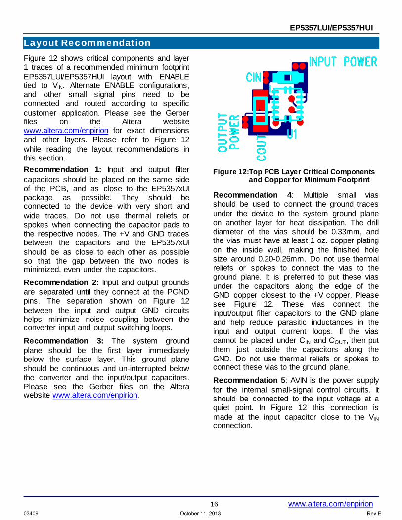
Layout Recommendation Figure 12 shows critical components and layer 1 traces of a recommended minimum footprint EP5357LUI/EP5357HUI layout with ENABLE tied to VIN. Alternate ENABLE configurations, and other small signal pins need to be connected and routed according to specific customer application. Please see the Gerber files on the Altera website www.altera.com/enpirion for exact dimensions and other layers. Please refer to Figure 12 while reading the layout recommendations in this section. Recommendation 1: Input and output filter capacitors should be placed on the same side of the PCB, and as close to the EP5357xUI package as possible. They should be connected to the device with very short and wide traces. Do not use thermal reliefs or spokes when connecting the capacitor pads to the respective nodes. The +V and GND traces between the capacitors and the EP5357xUI should be as close to each other as possible so that the gap between the two nodes is minimized, even under the capacitors.
Recommendation 2: Input and output grounds are separated until they connect at the PGND pins. The separation shown on Figure 12 between the input and output GND circuits helps minimize noise coupling between the converter input and output switching loops.
Recommendation 3: The system ground plane should be the first layer immediately below the surface layer. This ground plane should be continuous and un-interrupted below the converter and the input/output capacitors. Please see the Gerber files on the Altera website www.altera.com/enpirion.
Figure 12:Top PCB Layer Critical Components
and Copper for Minimum Footprint
Recommendation 4: Multiple small vias should be used to connect the ground traces under the device to the system ground plane on another layer for heat dissipation. The drill diameter of the vias should be 0.33mm, and the vias must have at least 1 oz. copper plating on the inside wall, making the finished hole size around 0.20-0.26mm. Do not use thermal reliefs or spokes to connect the vias to the ground plane. It is preferred to put these vias under the capacitors along the edge of the GND copper closest to the +V copper. Please see Figure 12. These vias connect the input/output filter capacitors to the GND plane and help reduce parasitic inductances in the input and output current loops. If the vias cannot be placed under CIN and COUT, then put them just outside the capacitors along the GND. Do not use thermal reliefs or spokes to connect these vias to the ground plane.
Recommendation 5: AVIN is the power supply for the internal small-signal control circuits. It should be connected to the input voltage at a quiet point. In Figure 12 this connection is made at the input capacitor close to the VIN connection.
16 www.altera.com/enpirion 03409 October 11, 2013 Rev E

EP5357LUI/EP5357HUI
Recommended PCB Footprint
Figure 13: EP5357 Package PCB Footprint
17 www.altera.com/enpirion 03409 October 11, 2013 Rev E
EP5357LUI/EP5357HUI
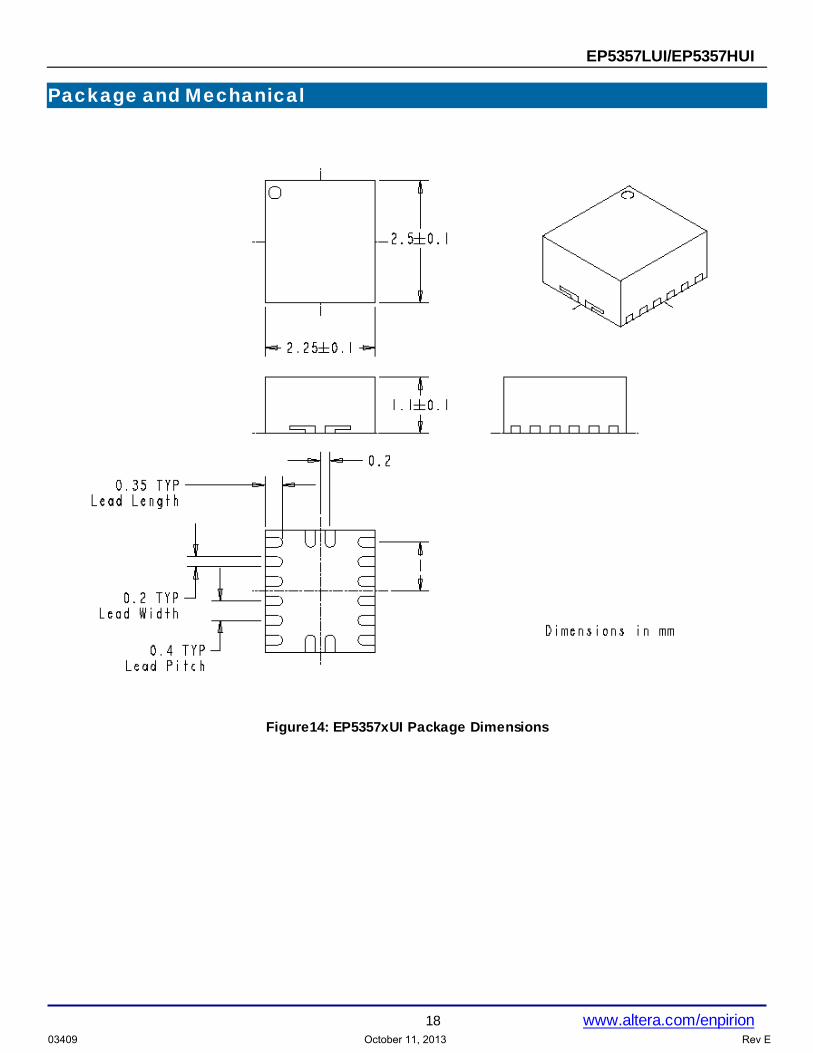
Package and Mechanical
Figure14: EP5357xUI Package Dimensions
18 www.altera.com/enpirion 03409 October 11, 2013 Rev E

EP5357LUI/EP5357HUI
Contact Information Altera Corporation 101 Innovation Drive San Jose, CA 95134 Phone: 408-544-7000 www.altera.com
© 2013 Altera Corporation—Confidential. All rights reserved. ALTERA, ARRIA, CYCLONE, ENPIRION, HARDCOPY, MAX, MEGACORE, NIOS, QUARTUS and STRATIX words and logos are trademarks of Altera Corporation and registered in the U.S. Patent and Trademark Office and in other countries. All other words and logos identified as trademarks or service marks are the property of their respective holders as described at www.altera.com/common/legal.html. Altera warrants performance of its semiconductor products to current specifications in accordance with Altera's standard warranty, but reserves the right to make changes to any products and services at any time without notice. Altera assumes no responsibil ity or l iability arising out of the application or use of any information, product, or service described herein except as expressly agreed to in writing by Altera. Altera customers are advised to obtain the latest version of device specifications before relying on any published information and before placing orders for products or services.
19 www.altera.com/enpirion 03409 October 11, 2013 Rev E
Related Documents