LTC3521 1 3521fb For more information www.linear.com/LTC3521 TYPICAL APPLICATION FEATURES APPLICATIONS DESCRIPTION 1A Buck-Boost DC/DC and Dual 600mA Buck DC/DC Converters The LTC ® 3521 combines a 1A buck-boost DC/DC converter and dual 600mA synchronous buck DC/DC converters. The 1.1MHz switching frequency minimizes the solution foot- print while maintaining high efficiency. All three converters feature soft-start and internal compensation to minimize the solution footprint and simplify the design process. The buck converters are current mode controlled and utilize an internal synchronous rectifier to improve ef- ficiency. The buck converters support 100% duty cycle operation to extend battery life. If the PWM pin is held low, the buck converters automatically transition from Burst Mode operation to PWM mode at high loads. With the PWM pin held high, the buck converters remain in low noise, 1.1MHz PWM mode. The buck-boost converter features continuous conduction operation to maximize efficiency and minimize noise. At light loads, the buck-boost converter can be operated in Burst Mode operation to improve efficiency and reduce no-load standby current. The LTC3521 provides a <2μA shutdown mode, over- temperature shutdown and current limit protection on all converters. The LTC3521 is available in a 24-pin 0.75mm × 4mm × 4mm QFN package, and a 20-pin ther- mally enhanced TSSOP package. n Three High Efficiency DC/DC Converters: Buck-Boost (V OUT : 1.8V to 5.25V, I OUT : 1A) Dual Buck (V OUT : 0.6V to V IN , I OUT : 600mA) n 1.8V to 5.5V Input Voltage Range n Pin-Selectable Burst Mode ® Operation n 30µA Total Quiescent Current in Burst Mode Operation n Independent Power Good Indicator Outputs n Integrated Soft-Start n Thermal and Overcurrent Protection n <2µA Current in Shutdown n Small 4mm × 4mm QFN and Thermally Enhanced TSSOP Packages n Bar Code Readers n Medical Instruments n Handy Terminals n PDAs, Handheld PCs n GPS Receivers + PV IN1 PV IN2 SW2 SW3 FB2 FB3 V OUT1 LTC3521 SHDN2 SHDN1 1.0M 137k 68.1k 22μF 10μF V IN 4.7μF Li-Ion 4.7μH 4.7μH V OUT1 3.3V 800mA (1A, V IN > 3.0V) V OUT2 1.8V 600mA 100k 100k 10μF 4.7μH V OUT3 1.2V 600mA V IN 2.4V TO 4.2V 221k 3521 TA01a SHDN3 PWM SW1A SW1B FB1 PGOOD2 PGOOD1 PGOOD3 PGND1A PGND2 GND PGND1B ON OFF PWM BURST V IN (V) 2.4 EFFICIENCY (%) 92 94 96 98 5.4 3521 TA01b 88 90 86 84 82 80 76 78 74 72 70 3.4 4.4 100 V OUT1 = 3.3V I OUT = 500mA V OUT2 = 1.8V I OUT = 200mA V OUT3 = 1.2V I OUT = 200mA Efficiency vs V IN L, LT, LTC, LTM, Linear Technology, Burst Mode and the Linear logo are registered trademarks and PowerPath is a trademark of Linear Technology Corporation. All other trademarks are the property of their respective owners. Protected by U. S. Patents, including 6404251, 6166527.

Welcome message from author
This document is posted to help you gain knowledge. Please leave a comment to let me know what you think about it! Share it to your friends and learn new things together.
Transcript

LTC3521
13521fb
For more information www.linear.com/LTC3521
Typical applicaTion
FeaTures
applicaTions
DescripTion
1A Buck-Boost DC/DC and Dual 600mA Buck
DC/DC Converters
The LTC®3521 combines a 1A buck-boost DC/DC converter and dual 600mA synchronous buck DC/DC converters. The 1.1MHz switching frequency minimizes the solution foot-print while maintaining high efficiency. All three converters feature soft-start and internal compensation to minimize the solution footprint and simplify the design process.
The buck converters are current mode controlled and utilize an internal synchronous rectifier to improve ef-ficiency. The buck converters support 100% duty cycle operation to extend battery life. If the PWM pin is held low, the buck converters automatically transition from Burst Mode operation to PWM mode at high loads. With the PWM pin held high, the buck converters remain in low noise, 1.1MHz PWM mode.
The buck-boost converter features continuous conduction operation to maximize efficiency and minimize noise. At light loads, the buck-boost converter can be operated in Burst Mode operation to improve efficiency and reduce no-load standby current.
The LTC3521 provides a <2μA shutdown mode, over- temperature shutdown and current limit protection on all converters. The LTC3521 is available in a 24-pin 0.75mm × 4mm × 4mm QFN package, and a 20-pin ther-mally enhanced TSSOP package.
n Three High Efficiency DC/DC Converters: Buck-Boost (VOUT: 1.8V to 5.25V, IOUT: 1A) Dual Buck (VOUT: 0.6V to VIN, IOUT: 600mA)n 1.8V to 5.5V Input Voltage Rangen Pin-Selectable Burst Mode® Operationn 30µA Total Quiescent Current in Burst Mode
Operationn Independent Power Good Indicator Outputsn Integrated Soft-Startn Thermal and Overcurrent Protectionn <2µA Current in Shutdownn Small 4mm × 4mm QFN and Thermally Enhanced
TSSOP Packages
n Bar Code Readersn Medical Instrumentsn Handy Terminalsn PDAs, Handheld PCsn GPS Receivers
+PVIN1 PVIN2
SW2
SW3
FB2
FB3
VOUT1
LTC3521
SHDN2SHDN1
1.0M
137k
68.1k22µF
10µF
VIN4.7µFLi-Ion
4.7µH 4.7µH
VOUT13.3V
800mA(1A, VIN > 3.0V)
VOUT21.8V600mA
100k
100k
10µF
4.7µH VOUT31.2V600mA
VIN2.4V TO 4.2V
221k
3521 TA01a
SHDN3PWM
SW1A
SW1B
FB1
PGOOD2PGOOD1
PGOOD3PGND1APGND2GNDPGND1B
ONOFF
PWMBURST
VIN (V)2.4
EFFI
CIEN
CY (%
)
92949698
5.4
3521 TA01b
8890
86848280
7678
747270
3.4 4.4
100
VOUT1 = 3.3VIOUT = 500mA
VOUT2 = 1.8VIOUT = 200mA
VOUT3 = 1.2VIOUT = 200mA
Efficiency vs VIN
L, LT, LTC, LTM, Linear Technology, Burst Mode and the Linear logo are registered trademarks and PowerPath is a trademark of Linear Technology Corporation. All other trademarks are the property of their respective owners. Protected by U. S. Patents, including 6404251, 6166527.
LTC3521
23521fb
For more information www.linear.com/LTC3521
pin conFiguraTion
absoluTe MaxiMuM raTingsPVIN1, PVIN2, VIN Voltage ............................. –0.3V to 6VSW1A, SW1B, SW2, SW3 Voltage DC ............................................................ –0.3V to 6V Pulsed < 100ns ............................................–1V to 7V
(Note 1)
LEAD FREE FINISH TAPE AND REEL PART MARKING* PACKAGE DESCRIPTION TEMPERATURE RANGE
LTC3521EFE#PBF LTC3521EFE#TRPBF LTC3521FE 20-Lead Plastic TSSOP –40°C to 125°C
LTC3521IFE#PBF LTC3521IFE#TRPBF LTC3521FE 20-Lead Plastic TSSOP –40°C to 125°C
LTC3521EUF#PBF LTC3521EUF#TRPBF 3521 24-Lead (4mm × 4mm) Plastic QFN –40°C to 125°C
LTC3521IUF#PBF LTC3521IUF#TRPBF 3521 24-Lead (4mm × 4mm) Plastic QFN –40°C to 125°C
Consult LTC Marketing for parts specified with wider operating temperature ranges. *The temperature grade is identified by a label on the shipping container.For more information on lead free part marking, go to: http://www.linear.com/leadfree/ For more information on tape and reel specifications, go to: http://www.linear.com/tapeandreel/
orDer inForMaTion
Voltage, All Other Pins ................................. –0.3V to 6VOperating Junction Temperature Range (Notes 2, 5) ............................................ –40°C to 125°CStorage Temperature Range .................. –65°C to 150°C
FE PACKAGE20-LEAD PLASTIC TSSOP
1
2
3
4
5
6
7
8
9
10
TOP VIEW
20
19
18
17
16
15
14
13
12
11
FB3
FB2
SHDN2
PGOOD3
PGOOD2
PGOOD1
VIN
GND
PWM
FB1
PVIN2
SW2
PGND2
SW3
VOUT1
SW1A
SW1B
PVIN1
SHDN1
SHDN3
21PGND1A
TJMAX = 150°C, θJA = 40°C/W (NOTE 4)
UNDERSIDE METAL INTERNALLY CONNECTED TO V– (PCB CONNECTION OPTIONAL)EXPOSED PAD (PIN 21) IS PGND1A AND MUST BE SOLDERED TO PCB GROUND
24 23 22 21 20 19
7 8 9
TOP VIEW
25PGND1A
UF PACKAGE24-LEAD (4mm × 4mm) PLASTIC QFN
10 11 12
6
5
4
3
2
1
13
14
15
16
17
18SHDN2
PGOOD3
PGOOD2
PGOOD1
VIN
GND
PGND2
SW3
VOUT1
SW1A
SW1B
NC
FB2
FB3
PVIN
2
PGND
1A
SW2
NC
PWM
FB1
SHDN
3
SHDN
1
PVIN
1
PGND
1B
TJMAX = 125°C, θJA = 37°C/W
EXPOSED PAD (PIN 25) IS PGND1A AND MUST BE SOLDERED TO PCB GROUND

LTC3521
33521fb
For more information www.linear.com/LTC3521
Note 1: Stresses beyond those listed under Absolute Maximum Ratings may cause permanent damage to the device. Exposure to any Absolute Maximum Rating condition for extended periods may affect device reliability and lifetime.Note 2: The LTC3521 is tested under pulsed load conditions such that TJ ≈ TA. The LTC3521E is guaranteed to meet performance specifica-
PARAMETER CONDITIONS MIN TYP MAX UNITS
Input Voltage l 1.8 5.5 V
Quiescent Current—Shutdown VSHDN1 = VSHDN2 = VSHDN3 = 0V (Note 6) l 0.01 2 µA
Burst Mode Quiescent Current VFB1 = 0.66V, VFB2 = 0.66V, VFB3 = 0.66V, VPWM = 0V 30 µA
Oscillator Frequency l 0.85 1.1 1.35 MHz
SHDN1, SHDN2, SHDN3, PWM Input High Voltage l 1.4 V
SHDN1, SHDN2, SHDN3, PWM Input Low Voltage l 0.4 V
Power Good Outputs Low Voltage IPGOOD1 = IPGOOD2 = IPGOOD3 = 1mA 0.1 0.2 V
Power Good Outputs Leakage Current VPGOOD1 = VPGOOD2 = VPGOOD3 = 5.5V 0.1 10 µA
Buck Converters
PMOS Switch Resistance 0.205 Ω
NMOS Switch Resistance 0.170 Ω
NMOS Switch Leakage Current VSW2 = VSW3 = 5.5V, VIN = 5.5V 0.1 5 µA
PMOS Switch Leakage Current VSW2 = VSW3 = 0V, VIN = 5.5V 0.1 10 µA
Feedback Voltage (Note 4) l 0.585 0.6 0.612 V
Feedback Input Current VFB2 = VFB3 = 0.6V 1 50 nA
PMOS Current Limit (Note 3) l 750 1050 mA
Maximum Duty Cycle VFB2 = VFB3 = 0.55V l 100 %
Minimum Duty Cycle VFB2 = VFB3 = 0.66V l 0 %
PGOOD Threshold VFB2,3 Falling –12 –9 –6 %
Power Good Hysteresis VFB2,3 Returning Good 2 %
Buck-Boost Converter
Output Voltage l 1.8 5.25 V
PMOS Switch Resistance 0.110 Ω
NMOS Switch Resistance 0.085 Ω
NMOS Switch Leakage Current VSW1A = VSW1B = 5.5V, VIN = 5.5V 0.1 5 µA
PMOS Switch Leakage Current VSW1A = VSW1B = 0V, VIN = 5.5V 0.1 10 µA
Feedback Voltage (Note 4) l 0.585 0.6 0.612 V
Feedback Input Current VFB1 = 0.6V 1 50 nA
Average Current Limit (Note 3) l 1.65 2.1 A
Reverse Current Limit (Note 3) 375 mA
Maximum Duty Cycle VFB1 = 0.55V l 85 94 %
Minimum Duty Cycle VFB1 = 0.66V l 0 %
PGOOD Threshold VFB1 Falling –12 –9 –6 %
Power Good Hysteresis VFB1 Returning Good 3 %
elecTrical characTerisTics The l denotes the specifications which apply over the full operating junction temperature range, otherwise specifications are at TA = 25°C (Note 2). VIN, PVIN1, PVIN2 = 3.6V, VOUT1 = 3.3V, unless otherwise noted.
tions from 0°C to 85°C. Specifications over the –40°C to 125°C operating junction temperature range are assured by design, characterization and correlation with statistical process controls. The LTC3521I is guaranteed over the full –40°C to 125°C operating junction temperature range. The maximum ambient temperature is determined by specific operating conditions in conjunction with board layout, the rated package thermal impedance and other environmental factors.

LTC3521
43521fb
For more information www.linear.com/LTC3521
Typical perForMance characTerisTics
Buck-Boost Efficiency vs Load Current, Li-Ion to 3.3V
Buck Efficiency vs Load Current, Li-Ion to 2.5V
Buck Efficiency vs Load Current, Li-Ion to 1.8V
Buck Burst Mode Current Threshold vs VIN
0.1 1 10 100 1000LOAD CURRENT (mA)
EFFI
CIEN
CY (%
)
POWER LOSS (m
W)
3521 G01
0
20
40
60
80
100
120
140
0
20
30
40
50
60
70
80
90
100
10
Burst ModeOPERATION
Burst ModePOWER LOSS
VIN = 2.7VVIN = 4.2V
PWM MODE
0.1 1 10 100 1000LOAD CURRENT (mA)
0
EFFI
CIEN
CY (%
)
POWER LOSS (m
W)
20
30
40
50
60
70
3521 G02
80
90
100
0
20
40
60
80
100
120
140
10
Burst ModeOPERATION
Burst ModePOWER LOSS
VIN = 3.6VVIN = 4.2V
PWM MODE
0.1 1 10 100 1000LOAD CURRENT (mA)
0
EFFI
CIEN
CY (%
)
POWER LOSS (m
W)
20
30
40
50
60
70
3521 G03
80
90
100
0
20
40
60
80
100
120
140
10
Burst ModeOPERATION
Burst ModePOWER LOSS
PWM MODE
VIN = 2.7VVIN = 4.2V
TA = 25°C, unless otherwise noted.
VIN (V)1.5
LOAD
CUR
RENT
(mA)
40
50
5
30
20
2.5 3.52 3 4 4.5 5.5
10
0
60
3521 G04
VOUT = 2.5V
VOUT = 1.8V
VOUT = 1.2V
elecTrical characTerisTicsNote 3: Current measurements are performed when the LTC3521 is not switching. The current limit values in operation will be somewhat higher due to the propagation delay of the comparators.Note 4: The LTC3521 is tested in a proprietary test mode that connects each FB pin to the output of the respective error amplifier.Note 5: This IC includes overtemperature protection that is intended to protect the device during momentary overload conditions. Junction
temperature will exceed 125°C when overtemperature protection is active. Continuous operation above the specified maximum operating junction temperature may impair device reliability.Note 6: Shutdown current is measured on the VIN pin and does not include PMOS switch leakage.

LTC3521
53521fb
For more information www.linear.com/LTC3521
Switching Frequency vs Temperature
Buck-Boost Feedback Voltage vs Temperature
Typical perForMance characTerisTics
Buck Feedback Voltage vs Temperature
Buck-Boost Maximum Load Current vs VIN, Burst Mode Operation
Buck-Boost Switches RDS(ON) vs Temperature
Buck Switches RDS(ON) vs Temperature
Switching Frequency vs VIN
TA = 25°C, unless otherwise noted.
Burst Mode Quiescent Current vs VIN
TEMPERATURE (°C)–40
R DS(
ON) (
mΩ
)
120
140
100
100
80
0 40–20 20 60 12080
20
0
60
160
40
3521 G05
PMOS(SWITCHES A AND D)
NMOS(SWITCHES B AND C)
VIN = 3.6VVOUT1 = 3.3V
TEMPERATURE (°C)–40
R DS(
ON) (
mΩ
)
300
100
250
200
0 40–20 20 60 12080
50
0
150
350
100
3521 G06
PMOS
NMOS
VIN = 3.6V
TEMPERATURE (°C)–50
–1.0
CHAN
GE F
ROM
25°
C (%
)
–0.8
–0.4
–0.2
0
1.0
0.4
–10 30 50
3521 G07
–0.6
0.6
0.8
0.2
–30 10 70 90 110
VIN (V)1.8
CHAN
GE F
ROM
VIN
= 3
.6V
(%)
1.0
1.5
5.3
0.5
0
2.8 3.82.3 3.3 4.3 4.8
–1.5
–2.0
–0.5
2.0
–1.0
3521 G08
TEMPERATURE (°C)–40
CHAN
GE IN
FEE
DBAC
K VO
LTAG
E FR
OM 2
5°C
(%)
0.1
100
0
–0.1
0 40–20 20 60 12080
–0.4
–0.5
–0.2
0.2
–0.3
3521 G09
TEMPERATURE (°C)
CHAN
GE IN
FEE
DBAC
K VO
LTAG
E FR
OM 2
5°C
(%)
–0.1
0
0.1
–0.2
–0.3
–0.4
–0.5
0.2
3521 G10
–50 –25 250 50 75 100 125
VIN (V)1.8
QUIE
SCEN
T CU
RREN
T (µ
A)
5.3
31
2.8 3.82.3 3.3 4.3 4.825
29
33
27
3521 G11
ALL THREE CONVERTERS ENABLED
VIN (V)1.8
MAX
IMUM
LOA
D CU
RREN
T (m
A)
60
70
80
5.3
50
40
2.8 3.82.3 3.3 4.3 4.8
10
0
30
90
20
3521 G12
VOUT = 3V
VOUT = 5V
Buck-Boost Maximum Load Current vs VIN, PWM Mode
100
500
900
1300
300
700
1100
1500
VIN (V)
LOAD
CUR
RENT
(mA)
3521 G13
VOUT = 3.3V
L = 4.7µH
VOUT = 5V
1.8 5.32.8 3.82.3 3.3 4.3 4.8
LTC3521
63521fb
For more information www.linear.com/LTC3521
Typical perForMance characTerisTics
Buck-Boost Current Limit vs Temperature
Buck Current Limitvs Temperature
TA = 25°C, unless otherwise noted.
Buck-Boost Peak Current Limit vs Temperature
TEMPERATURE (°C)
CURR
ENT
LIM
IT (m
A)
2100
2050
2000
1950
2150
3521 G19
–50 –25 250 50 75 100 125TEMPERATURE (°C)
CURR
ENT
LIM
IT (m
A)
3300
3250
3200
3350
3521 G20
–50 –25 250 50 75 100 125TEMPERATURE (°C)
CURR
ENT
LIM
IT (m
A)
1100
1050
1000
950
900
1150
3521 G21
–50 –25 250 50 75 100 125
50µs/DIV
VOUT20mV/DIV
INDUCTORCURRENT
200mA/DIV
3521 G16
VIN = 3.6VVOUT = 3.3V
L = 4.7µHCOUT = 22µF
Buck-Boost Burst Mode Operation to PWM Transition
Buck Load Step, PWM Mode, 10mA to 400mA
Buck Load Step, Burst Mode, 10mA to 400mA
100µs/DIV
VOUT100mV/DIV
INDUCTORCURRENT
200mA/DIV
3521 G17
VIN = 3.6VVOUT = 1.8V
L = 4.7µHCOUT = 10µF
100µs/DIV
VOUT100mV/DIV
INDUCTORCURRENT
200mA/DIV
3521 G18
VIN = 3.6VVOUT = 1.8V
L = 4.7µHCOUT = 10µF
No Load Quiescent Current vs VIN
100µs/DIV
VOUT100mV/DIV
INDUCTORCURRENT
500mA/DIV3521 G15
VIN = 3.6V, VOUT = 3.3VL = 4.7µHCOUT = 22µF
Buck-Boost Load Step, 0mA to 750mA
VIN (V)1.8
QUIE
SCEN
T CU
RREN
T (µ
A)
5.32.8 3.82.3 3.3 4.3 4.8
45
40
55
60
50
3521 G14
LTC3521
73521fb
For more information www.linear.com/LTC3521
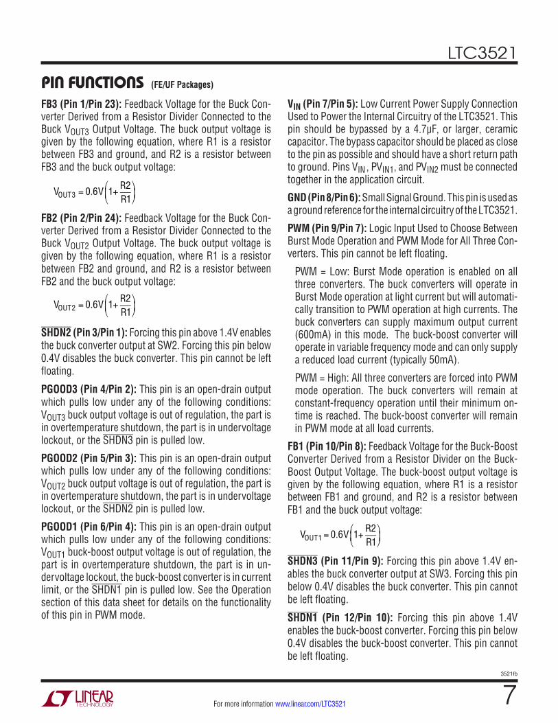
pin FuncTionsFB3 (Pin 1/Pin 23): Feedback Voltage for the Buck Con-verter Derived from a Resistor Divider Connected to the Buck VOUT3 Output Voltage. The buck output voltage is given by the following equation, where R1 is a resistor between FB3 and ground, and R2 is a resistor between FB3 and the buck output voltage:
VOUT3 = 0.6V 1+
R2R1
⎛
⎝⎜
⎞
⎠⎟
FB2 (Pin 2/Pin 24): Feedback Voltage for the Buck Con-verter Derived from a Resistor Divider Connected to the Buck VOUT2 Output Voltage. The buck output voltage is given by the following equation, where R1 is a resistor between FB2 and ground, and R2 is a resistor between FB2 and the buck output voltage:
VOUT2 = 0.6V 1+
R2R1
⎛
⎝⎜
⎞
⎠⎟
SHDN2 (Pin 3/Pin 1): Forcing this pin above 1.4V enables the buck converter output at SW2. Forcing this pin below 0.4V disables the buck converter. This pin cannot be left floating.
PGOOD3 (Pin 4/Pin 2): This pin is an open-drain output which pulls low under any of the following conditions: VOUT3 buck output voltage is out of regulation, the part is in overtemperature shutdown, the part is in undervoltage lockout, or the SHDN3 pin is pulled low.
PGOOD2 (Pin 5/Pin 3): This pin is an open-drain output which pulls low under any of the following conditions: VOUT2 buck output voltage is out of regulation, the part is in overtemperature shutdown, the part is in undervoltage lockout, or the SHDN2 pin is pulled low.
PGOOD1 (Pin 6/Pin 4): This pin is an open-drain output which pulls low under any of the following conditions: VOUT1 buck-boost output voltage is out of regulation, the part is in overtemperature shutdown, the part is in un-dervoltage lockout, the buck-boost converter is in current limit, or the SHDN1 pin is pulled low. See the Operation section of this data sheet for details on the functionality of this pin in PWM mode.
VIN (Pin 7/Pin 5): Low Current Power Supply Connection Used to Power the Internal Circuitry of the LTC3521. This pin should be bypassed by a 4.7µF, or larger, ceramic capacitor. The bypass capacitor should be placed as close to the pin as possible and should have a short return path to ground. Pins VIN , PVIN1, and PVIN2 must be connected together in the application circuit.
GND (Pin 8/Pin 6): Small Signal Ground. This pin is used as a ground reference for the internal circuitry of the LTC3521.
PWM (Pin 9/Pin 7): Logic Input Used to Choose Between Burst Mode Operation and PWM Mode for All Three Con-verters. This pin cannot be left floating.
PWM = Low: Burst Mode operation is enabled on all three converters. The buck converters will operate in Burst Mode operation at light current but will automati-cally transition to PWM operation at high currents. The buck converters can supply maximum output current (600mA) in this mode. The buck-boost converter will operate in variable frequency mode and can only supply a reduced load current (typically 50mA).
PWM = High: All three converters are forced into PWM mode operation. The buck converters will remain at constant-frequency operation until their minimum on-time is reached. The buck-boost converter will remain in PWM mode at all load currents.
FB1 (Pin 10/Pin 8): Feedback Voltage for the Buck-Boost Converter Derived from a Resistor Divider on the Buck-Boost Output Voltage. The buck-boost output voltage is given by the following equation, where R1 is a resistor between FB1 and ground, and R2 is a resistor between FB1 and the buck output voltage:
VOUT1 = 0.6V 1+
R2R1
⎛
⎝⎜
⎞
⎠⎟
SHDN3 (Pin 11/Pin 9): Forcing this pin above 1.4V en-ables the buck converter output at SW3. Forcing this pin below 0.4V disables the buck converter. This pin cannot be left floating.
SHDN1 (Pin 12/Pin 10): Forcing this pin above 1.4V enables the buck-boost converter. Forcing this pin below 0.4V disables the buck-boost converter. This pin cannot be left floating.
(FE/UF Packages)
LTC3521
83521fb
For more information www.linear.com/LTC3521
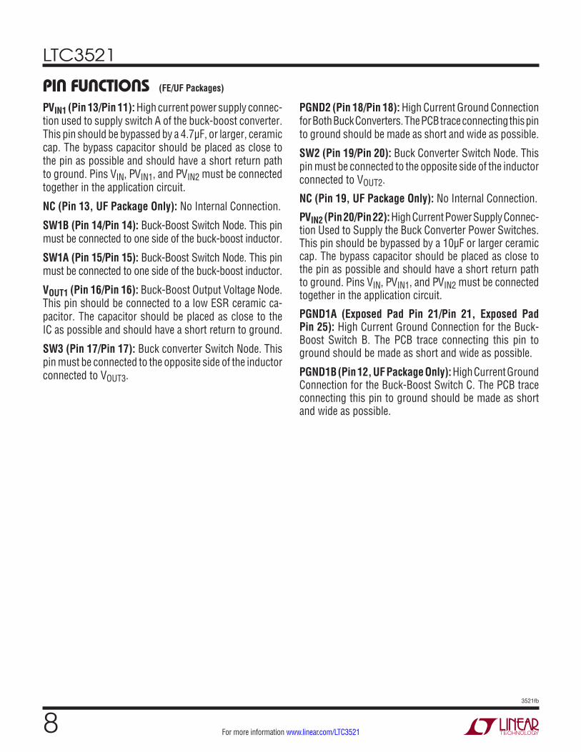
PVIN1 (Pin 13/Pin 11): High current power supply connec-tion used to supply switch A of the buck-boost converter. This pin should be bypassed by a 4.7µF, or larger, ceramic cap. The bypass capacitor should be placed as close to the pin as possible and should have a short return path to ground. Pins VIN, PVIN1, and PVIN2 must be connected together in the application circuit.
NC (Pin 13, UF Package Only): No Internal Connection.
SW1B (Pin 14/Pin 14): Buck-Boost Switch Node. This pin must be connected to one side of the buck-boost inductor.
SW1A (Pin 15/Pin 15): Buck-Boost Switch Node. This pin must be connected to one side of the buck-boost inductor.
VOUT1 (Pin 16/Pin 16): Buck-Boost Output Voltage Node. This pin should be connected to a low ESR ceramic ca-pacitor. The capacitor should be placed as close to the IC as possible and should have a short return to ground.
SW3 (Pin 17/Pin 17): Buck converter Switch Node. This pin must be connected to the opposite side of the inductor connected to VOUT3.
PGND2 (Pin 18/Pin 18): High Current Ground Connection for Both Buck Converters. The PCB trace connecting this pin to ground should be made as short and wide as possible.
SW2 (Pin 19/Pin 20): Buck Converter Switch Node. This pin must be connected to the opposite side of the inductor connected to VOUT2.
NC (Pin 19, UF Package Only): No Internal Connection.
PVIN2 (Pin 20/Pin 22): High Current Power Supply Connec-tion Used to Supply the Buck Converter Power Switches. This pin should be bypassed by a 10µF or larger ceramic cap. The bypass capacitor should be placed as close to the pin as possible and should have a short return path to ground. Pins VIN, PVIN1, and PVIN2 must be connected together in the application circuit.
PGND1A (Exposed Pad Pin 21/Pin 21, Exposed Pad Pin 25): High Current Ground Connection for the Buck-Boost Switch B. The PCB trace connecting this pin to ground should be made as short and wide as possible.
PGND1B (Pin 12, UF Package Only): High Current Ground Connection for the Buck-Boost Switch C. The PCB trace connecting this pin to ground should be made as short and wide as possible.
pin FuncTions (FE/UF Packages)
LTC3521
93521fb
For more information www.linear.com/LTC3521
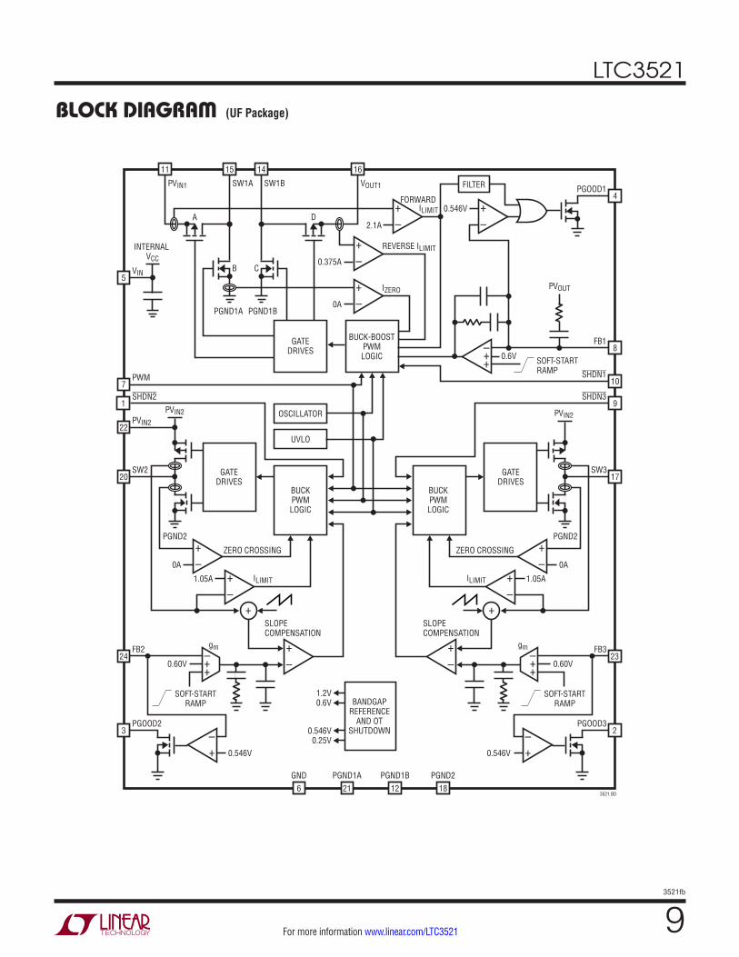
block DiagraM
+–
+–
PGOOD1
PVOUT
4
16
FB1
SHDN1
FILTER
REVERSE ILIMIT
FORWARD ILIMIT
21
0.546V
2.1A
0.375A
+–
+–0A
IZERO
BUCK-BOOSTPWMLOGIC
GATEDRIVES
GATEDRIVES
BUCKPWMLOGIC
BANDGAPREFERENCE
AND OTSHUTDOWN
OSCILLATOR
UVLO
0.6V SOFT-STARTRAMP
++–
SOFT-STARTRAMP
10
SHDN21
SHDN39
8
D
VOUT1
14
SW1B
15
SW1A
11
PVIN1
22PVIN2
CB
A
PGND1BPGND1A
PGND2
ZERO CROSSING
5VIN
7PWM
INTERNAL VCC
20SW2
FB2
+–0A
+–
+–
1.05A ILIMIT
0.546V
3521 BD
0.60V
gm
PGND1A6
GND12
PGND1B18
PGND2
SLOPECOMPENSATION
++–
24
PGOOD2
+
+–
1.2V0.6V
0.546V0.25V
3
PVIN2
GATEDRIVES
BUCKPWMLOGIC
SOFT-STARTRAMP
PGND2
ZERO CROSSING
17SW3
FB3
+– 0A
+–
+–
1.05AILIMIT
0.546V
0.60V
gm
SLOPECOMPENSATION
++–
23
PGOOD3
+
+– 2
PVIN2
(UF Package)
LTC3521
103521fb
For more information www.linear.com/LTC3521
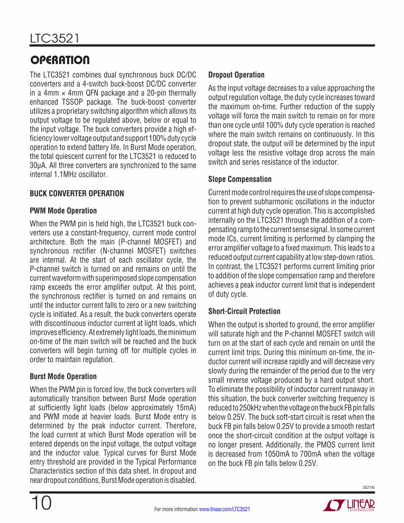
operaTionThe LTC3521 combines dual synchronous buck DC/DC converters and a 4-switch buck-boost DC/DC converter in a 4mm × 4mm QFN package and a 20-pin thermally enhanced TSSOP package. The buck-boost converter utilizes a proprietary switching algorithm which allows its output voltage to be regulated above, below or equal to the input voltage. The buck converters provide a high ef-ficiency lower voltage output and support 100% duty cycle operation to extend battery life. In Burst Mode operation, the total quiescent current for the LTC3521 is reduced to 30μA. All three converters are synchronized to the same internal 1.1MHz oscillator.
BUCK CONVERTER OPERATION
PWM Mode Operation
When the PWM pin is held high, the LTC3521 buck con-verters use a constant-frequency, current mode control architecture. Both the main (P-channel MOSFET) and synchronous rectifier (N-channel MOSFET) switches are internal. At the start of each oscillator cycle, the P-channel switch is turned on and remains on until the current waveform with superimposed slope compensation ramp exceeds the error amplifier output. At this point, the synchronous rectifier is turned on and remains on until the inductor current falls to zero or a new switching cycle is initiated. As a result, the buck converters operate with discontinuous inductor current at light loads, which improves efficiency. At extremely light loads, the minimum on-time of the main switch will be reached and the buck converters will begin turning off for multiple cycles in order to maintain regulation.
Burst Mode Operation
When the PWM pin is forced low, the buck converters will automatically transition between Burst Mode operation at sufficiently light loads (below approximately 15mA) and PWM mode at heavier loads. Burst Mode entry is determined by the peak inductor current. Therefore, the load current at which Burst Mode operation will be entered depends on the input voltage, the output voltage and the inductor value. Typical curves for Burst Mode entry threshold are provided in the Typical Performance Characteristics section of this data sheet. In dropout and near dropout conditions, Burst Mode operation is disabled.
Dropout Operation
As the input voltage decreases to a value approaching the output regulation voltage, the duty cycle increases toward the maximum on-time. Further reduction of the supply voltage will force the main switch to remain on for more than one cycle until 100% duty cycle operation is reached where the main switch remains on continuously. In this dropout state, the output will be determined by the input voltage less the resistive voltage drop across the main switch and series resistance of the inductor.
Slope Compensation
Current mode control requires the use of slope compensa-tion to prevent subharmonic oscillations in the inductor current at high duty cycle operation. This is accomplished internally on the LTC3521 through the addition of a com-pensating ramp to the current sense signal. In some current mode ICs, current limiting is performed by clamping the error amplifier voltage to a fixed maximum. This leads to a reduced output current capability at low step-down ratios. In contrast, the LTC3521 performs current limiting prior to addition of the slope compensation ramp and therefore achieves a peak inductor current limit that is independent of duty cycle.
Short-Circuit Protection
When the output is shorted to ground, the error amplifier will saturate high and the P-channel MOSFET switch will turn on at the start of each cycle and remain on until the current limit trips. During this minimum on-time, the in-ductor current will increase rapidly and will decrease very slowly during the remainder of the period due to the very small reverse voltage produced by a hard output short. To eliminate the possibility of inductor current runaway in this situation, the buck converter switching frequency is reduced to 250kHz when the voltage on the buck FB pin falls below 0.25V. The buck soft-start circuit is reset when the buck FB pin falls below 0.25V to provide a smooth restart once the short-circuit condition at the output voltage is no longer present. Additionally, the PMOS current limit is decreased from 1050mA to 700mA when the voltage on the buck FB pin falls below 0.25V.

LTC3521
113521fb
For more information www.linear.com/LTC3521
Soft-Start
The buck converters have an internal voltage mode soft-start circuit with a nominal duration of 800μs. The converters remain in regulation during soft-start and will therefore respond to output load transients which occur during this time. In addition, the output voltage rise time has minimal dependency on the size of the output capaci-tor or load current.
Error Amplifier and Compensation
The LTC3521 buck converters utilize an internal transcon-ductance error amplifier. Compensation of the feedback loop is performed internally to reduce the size of the application circuit and simplify the design process. The compensation network has been designed to allow use of a wide range of output capacitors while simultaneously ensuring rapid response to load transients.
PGOOD Comparators
The PGOOD2 and PGOOD3 pins are open-drain outputs which indicate the status of the buck converters. If the buck output voltage falls 9% below the regulation voltage, the respective PGOOD open-drain output will pull low. The output voltage must rise 2% above the falling threshold before the pull-down will turn off. In addition, there is a 60μs typical deglitching delay in the flag in order to prevent false trips due to voltage transients on load steps. The respective PGOOD output will also pull low during overtemperature shutdown, undervoltage lockout or if the respective buck con-verter SHDN pin is pulled low to indicate these fault conditions.
BUCK-BOOST CONVERTER OPERATION
PWM Mode Operation
When the PWM pin is held high, the LTC3521 buck-boost converter operates in a constant-frequency PWM mode with voltage mode control. A proprietary switching algo-rithm allows the converter to switch between buck, buck-boost and boost modes without discontinuity in inductor current or loop characteristics. The switch topology for the buck-boost converter is shown in Figure 1.
When the input voltage is significantly greater than the output voltage, the buck-boost converter operates in buck mode. Switch D turns on continuously and switch C remains off. Switches A and B are pulse width modu-lated to produce the required duty cycle to support the output regulation voltage. As the input voltage decreases, switch A remains on for a larger portion of the switching cycle. When the duty cycle reaches approximately 85%, the switch pair AC begins turning on for a small fraction of the switching period. As the input voltage decreases further, the AC switch pair remains on for longer durations and the duration of the BD phase decreases proportion-ally. As the input voltage drops below the output voltage, the AC phase will eventually increase to the point that there is no longer any BD phase. At this point, switch A remains on continuously while switch pair CD is pulse width modulated to obtain the desired output voltage. At this point, the converter is operating solely in boost mode.
This switching algorithm provides a seamless transition between operating modes and eliminates discontinuities in average inductor current, inductor current ripple and loop transfer function throughout all three operational
operaTion
L
D
PGND1BPGND1ALTC3521
A SW1A SW1B
B C
3521 F01
VOUT1PVIN1
Figure 1. Buck-Boost Switch Topology

LTC3521
123521fb
For more information www.linear.com/LTC3521
modes. These advantages result in increased efficiency and stability in comparison to the traditional 4-switch buck-boost converter.
Error Amplifier and Compensation
The buck-boost converter utilizes a voltage mode error amplifier with an internal compensation network as shown in Figure 2.
this case, the increased bandwidth created by decreasing R2 is used to counteract the reduced converter bandwidth caused by the large output capacitor.
Current Limit Operation
The buck-boost converter has two current limit circuits. The primary current limit is an average current limit circuit which injects an amount of current into the feedback node which is proportional to the extent that the switch A cur-rent exceeds the current limit value. Due to the high gain of this loop, the injected current forces the error amplifier output to decrease until the average current through switch A decreases approximately to the current limit value. The average current limit utilizes the error amplifier in an active state and thereby provides a smooth recovery with little overshoot once the current limit fault condition is removed. Since the current limit is based on the average current through switch A, the peak inductor current in current limit will have a dependency on the duty cycle (i.e., on the input and output voltages in the overcurrent condition).
The speed of the average current limit circuit is limited by the dynamics of the error amplifier. On a hard output short, it would be possible for the inductor current to increase substantially beyond current limit before the average cur-rent limit circuit would react. For this reason, there is a second current limit circuit which turns off switch A if the current ever exceeds approximately 165% of the average current limit value. This provides additional protection in the case of an instantaneous hard output short.
Reverse Current Limit
The reverse current comparator on switch D monitors the inductor current entering PVOUT. When this current exceeds 375mA (typical), switch D will be turned off for the remainder of the switching cycle.
operaTion
0.6V
GND
PVOUTLTC3521
VOUT
FB1R2
R1
3521 F02
+–
Figure 2. Buck-Boost Error Amplifier and Compensation
Notice that resistor R2 of the external resistor divider network plays an integral role in determining the frequency response of the compensation network. The ratio of R2 to R1 must be set to program the desired output voltage but this still allows the value of R2 to be adjusted to optimize the transient response of the converter. Increasing the value of R2 generally leads to greater stability at the expense of reduced transient response speed. Increasing the value of R2 can yield substantial transient response improvement in cases where the phase margin has been reduced due to the use of a small value output capacitor or a large inductance (particularly with large boost step-up ratios). Conversely, decreasing the value of R2 increases the loop bandwidth which can improve the speed of the converter’s transient response. This can be useful in improving the transient response if a large valued output capacitor is utilized. In
LTC3521
133521fb
For more information www.linear.com/LTC3521
Burst Mode Operation
With the PWM pin held low, the buck-boost converter operates utilizing a variable frequency switching algorithm designed to improve efficiency at light load and reduce the standby current at zero load. In Burst Mode operation, the inductor is charged with fixed peak amplitude current pulses. These current pulses are repeated as often as necessary to maintain the output regulation voltage. The maximum output current which can be supplied in Burst Mode operation is dependent upon the input and output voltage as given by the following formula:
IOUT(MAX),BURST =
0.1• VINVIN + VOUT
A( )
In Burst Mode operation, the error amplifier is not used but is instead placed in a low current standby mode to reduce supply current and improve light load efficiency.
Soft-Start
The buck-boost converter has an internal voltage mode soft-start circuit with a nominal duration of 600μs. The converter remains in regulation during soft-start and will therefore respond to output load transients that occur during this time. In addition, the output voltage rise time has minimal dependency on the size of the output capaci-tor or load. During soft-start, the buck-boost converter is forced into PWM operation regardless of the state of the PWM pin.
PGOOD Comparator
The PGOOD1 pin is an open-drain output which indicates the status of the buck-boost converter. In Burst Mode operation (PWM = Low), the PGOOD1 open-drain output will pull low when the feedback voltage falls 9% below the regulation voltage. There is approximately 3% hysteresis in this threshold when the output voltage is returning good. In addition, there is a 60μs typical deglitching delay to prevent false trips due to short duration voltage transients in response to load steps.
In PWM mode, operation of the PGOOD1 comparator is complicated by the fact that the feedback pin voltage is driven to the reference voltage independent of the output
operaTionvoltage through the action of the voltage mode error am-plifier. Since the soft-start is voltage mode, the feedback voltage will track the output voltage correctly during soft-start, and the PGOOD1 output will correctly indicate the point at which the buck-boost attains regulation at the end of soft-start. Therefore, the PGOOD1 output can be utilized for sequencing purposes. Once in regulation, the feedback voltage will no longer track the output voltage, and the PGOOD1 pin will not directly respond to a loss of regulation in the output. However, the only means by which a loss of regulation can occur is if the current limit has been reached, thereby preventing the buck-boost converter from delivering the required output current. In such cases, the occurrence of current limit will cause the PGOOD1 flag to fall indicating a fault state. There can be cases, however, when the buck-boost converter is continuously in current limit, causing the PGOOD1 output to pull low, while the output voltage still remains slightly above the PGOOD1 comparator trip point.
The PGOOD1 output also pulls low during overtemperature shutdown, undervoltage lockout or if the SHDN1 pin is pulled low.
COMMON FUNCTIONS
Thermal Shutdown
If the die temperature exceeds 150°C, all three converters will be disabled. All power devices will be turned off and all switch nodes will be high impedance. The soft-start circuits for all three converters are reset during thermal shutdown to provide a smooth recovery once the over-temperature condition is eliminated. All three converters will restart (if enabled) when the die temperature drops to approximately 140°C.
Undervoltage Lockout
If the supply voltage decreases below 1.7V (typical) then all three converters will be disabled and all power devices will be turned off. The soft-start circuits for all three con-verters are reset during undervoltage lockout to provide a smooth restart once the input voltage rises above the undervoltage lockout threshold.

LTC3521
143521fb
For more information www.linear.com/LTC3521
applicaTions inForMaTionThe basic LTC3521 application circuit is shown as the Typical Application on the front page of this data sheet. The external component selection is determined by the desired output voltages, output currents and ripple volt-age requirements of each particular application. Basic guidelines and considerations for the design process are provided in this section.
Buck Inductor Selection
The choice of buck inductor value influences both the ef-ficiency and the magnitude of the output voltage ripple. Larger inductance values will reduce inductor current ripple and lead to lower output voltage ripple. For a fixed DC resistance, a larger value inductor will yield higher efficiency by lowering the peak current closer to the av-erage. However, a larger inductor within the same family will generally have a greater series resistance, thereby offsetting this efficiency advantage.
Given a desired peak-to-peak current ripple, ΔIL, the required inductance can be calculated via the following expression, where f represents the switching frequency in MHz:
L =
1fΔIL
VOUT 1–VOUTVIN
⎛
⎝⎜
⎞
⎠⎟ µH( )
A reasonable choice for ripple current is ΔIL = 240mA which represents 40% of the maximum 600mA load current. The DC current rating of the inductor should be at least equal to the maximum load current, plus half the ripple current, in order to prevent core saturation and loss of efficiency during operation. To optimize efficiency, the inductor should have a low series resistance.
In particularly space-restricted applications, it may be advantageous to use a much smaller value inductor at the expense of larger ripple current. In such cases, the converter will operate in discontinuous conduction for a wider range of output loads and efficiency will be reduced. In addition, there is a minimum inductor value required to maintain stability of the current loop (given the fixed internal slope compensation). Specifically, if the buck converter is going to be utilized at duty cycles over 40%, the inductance value must be at least LMIN, as given by the following equation:
LMIN = 2.5 • VOUT (µH)
Table 1 depicts the recommended inductance for several common output voltages.
Table 1. Buck Recommended Inductance
OUTPUT VOLTAGEMINIMUM
INDUCTANCE MAXIMUM
INDUCTANCE
0.6V 1.5μH 2.2μH
1.2V 2.2μH 4.7μH
1.8V 3.3μH 6.8μH
2.5V 4.7μH 8.2μH
Buck Output Capacitor Selection
A low ESR output capacitor should be utilized at the buck output in order to minimize voltage ripple. Multilayer ce-ramic capacitors are an excellent choice as they have low ESR and are available in small footprints. In addition to controlling the ripple magnitude, the value of the output capacitor also sets the loop crossover frequency and can, therefore, impact loop stability. There is both a minimum and maximum capacitance value required to ensure stabil-ity of the loop. If the output capacitance is too small, the loop crossover frequency will increase to the point where the switching delay and the high frequency parasitic poles of the error amplifier will degrade the phase margin. In addition, the wider bandwidth produced by a small output capacitor will make the loop more susceptible to switch-ing noise. At the other extreme, if the output capacitor is too large, the crossover frequency can decrease too far below the compensation zero and lead to a degraded phase margin. Table 2 provides a guideline for the range of allowable values of low ESR output capacitors. Larger value output capacitors can be accommodated provided they have sufficient ESR to stabilize the loop.
Table 2. Buck Output Capacitor RangeVOUT CMIN CMAX
0.6V 15μF 300μF
0.8V 15μF 230μF
1.2V 10μF 150μF
1.8V 10μF 90μF
2.7V 10μF 70μF
3.3V 6.8μF 50μF

LTC3521
153521fb
For more information www.linear.com/LTC3521
Buck Input Capacitor Selection
The PVIN2 pin provides current to the buck converter power switch and is the supply pin for the IC’s internal circuitry. It is recommended that a low ESR ceramic capacitor with a value of at least 4.7µF be used to bypass this pin. The capacitor should be placed as close to the pin as possible and have a short return to ground.
Buck Output Voltage Programming
The output voltage is set by a resistive divider, according to the following formula:
VOUT2,3 = 0.6V 1+
R2R1
⎛
⎝⎜
⎞
⎠⎟
The external divider is connected to the output, as shown in Figure 3. It is recommended that a feedforward capaci-tor, CFF , be placed in parallel with resistor R2 to improve the noise immunity of the feedback node. Table 3 provides the recommended resistor and feedforward capacitor combinations for common output voltage options.
Table 3. Buck Resistor Divider ValuesVOUT R1 R2 CFF
0.6V – 0 –
0.8V 200k 69.8k 22pF
1.0V 118k 80.6k 22pF
1.2V 100k 102k 22pF
1.5V 78.7k 121k 22pF
1.8V 68.1k 137k 22pF
2.7V 63.4k 226k 33pF
3.3V 60.4k 274k 33pF
Buck-Boost Output Voltage Programming
The buck-boost output voltage is set by a resistive divider according to the following formula:
VOUT1 = 0.6V 1+
R2R1
⎛
⎝⎜
⎞
⎠⎟
The external divider is connected to the output, as shown in Figure 4. The buck-boost converter utilizes voltage mode control and the value of R2 plays an integral role in the dynamics of the feedback loop. In general, a larger value for R2 will increase stability and reduce the speed of the transient response. A smaller value of R2 will reduce stability but increase the transient response speed. A good starting point is to choose R2 = 1MΩ, then calculate the required value of R1 to set the desired output voltage ac-cording to the above formula. If a large output capacitor is used, the bandwidth of the converter is reduced. In such cases R2 can be reduced to improve the transient response. If a large inductor or small output capacitor is utilized, the loop will be less stable and the phase margin can be improved by increasing the value of R2.
Buck-Boost Inductor Selection
To achieve high efficiency, a low ESR inductor should be utilized for the buck-boost converter. The inductor must have a saturation rating greater than the worst case average inductor current plus half the ripple current. The peak-to-peak inductor current ripple will be larger in buck and boost mode than in the buck-boost region. The peak-to-peak inductor current ripple for each mode can
applicaTions inForMaTion
LTC3521
GND
0.6V ≤ VOUT3 ≤ 5.25V0.6V ≤ VOUT2 ≤ 5.25V
FB3
R1
3521 F03
R2
FB2
R1
R2
Figure 3. Setting the Buck Output Voltage
LTC3521
GND
1.8V ≤ VOUT1 ≤ 5.25V
FB1
R1
3521 F04
R2
Figure 4. Setting the Buck-Boost Output Voltage

LTC3521
163521fb
For more information www.linear.com/LTC3521
be calculated from the following formulas, where f is the frequency in MHz and L is the inductance in μH:
ΔIL,P-P,BUCK =1fL
•VOUT VIN – VOUT( )
VIN
ΔIL,P-P,BOOST =1fL
•VIN VOUT – VIN( )
VOUT
In addition to affecting output current ripple, the size of the inductor can also affect the stability of the feedback loop. In boost mode, the converter transfer function has a right half plane zero at a frequency that is inversely proportional to the value of the inductor. As a result, a large inductor can move this zero to a frequency that is low enough to degrade the phase margin of the feedback loop. It is recommended that the chosen inductor value be less than 10μH if the buck-boost converter is to be used in the boost region.
Buck-Boost Output Capacitor Selection
A low ESR output capacitor should be utilized at the buck-boost converter output in order to minimize output volt-age ripple. Multilayer ceramic capacitors are an excellent choice as they have low ESR and are available in small footprints. The capacitor should be chosen large enough to reduce the output voltage ripple to acceptable levels. Neglecting the capacitor ESR and ESL, the peak-to-peak output voltage ripple can be calculated by the following formulas, where f is the frequency in MHz, COUT is the capacitance in μF, L is the inductance in μH and ILOAD is the output current in amps:
ΔVP-P,BOOST =ILOAD VOUT – VIN( )
COUT • VOUT • f
ΔVP-P,BUCK =1
8 •L • COUT • f2 •VIN – VOUT( )VOUT
VIN
Since the output current is discontinuous in boost mode, the ripple in this mode will generally be much larger than the magnitude of the ripple in buck mode. In addition to controlling the ripple magnitude, the value of the output capacitor also affects the location of the resonant frequency in the open loop converter transfer function. If the output capacitor is too small, the bandwidth of the converter will extend high enough to degrade the phase margin. To prevent this from happening, it is recommended that a minimum value of 10μF be used for the buck-boost output capacitor.
Buck-Boost Input Capacitor Selection
The supply current to the buck-boost converter is provided by the PVIN1 pin. It is recommended that a low ESR ceramic capacitor with a value of at least 4.7μF be located as close to this pin as possible.
Inductor Style and Core Material
Different inductor core materials and styles have an impact on the size and price of an inductor at any given peak current rating. Toroid or shielded pot cores in ferrite or permalloy materials are small and reduce emissions, but generally cost more than powdered iron core induc-tors with similar electrical characteristics. The choice of inductor style depends upon the price, sizing, and EMI requirements of a particular application. Table 4 provides a sampling of inductors that are well suited to many LTC3521 application circuits.
Table 4. Representative Surface Mount InductorsMANU-FACTURER
PART NUMBER
VALUE
MAX CURRENT
DCR
HEIGHT
Taiyo Yuden NP03SB4R7M 4.7μH 1.2A 0.047Ω 1.8mm
NP03SB6R8M 6.8μH 1A 0.084Ω 1.8mm
Coilcraft MSS7341-502NL 5μH 2.3A 0.024Ω 4.1mm
DT1608C-472ML 4.7µH 1.2A 0.085Ω 2.92mm
Cooper-Bussmann
SD7030-5R0-R 5µH 2.4A 0.026Ω 3mm
SD20-6R2-R 6.2µH 1.12A 0.072Ω 2mm
Sumida CDR6D23MNNP-4R2 4.2µH 2.6A 0.052Ω 2.5mm
CDRH4D16FB/ND-6R8N
6.8µH 1A 0.081Ω 1.8mm
applicaTions inForMaTion

LTC3521
173521fb
For more information www.linear.com/LTC3521
applicaTions inForMaTionCapacitor Vendor Information
Both the input and output capacitors used with the LTC3521 must be low ESR and designed to handle the large AC cur-rents generated by switching converters. The vendors in Table 5 provide capacitors that are well suited to LTC3521 application circuits.
Table 5. Capacitor Vendor Information MANUFACTURER
WEB SITE
REPRESENTATIVE PART NUMBERS
Taiyo Yuden www.t-yuden.com JMK212BJ106K 10μF, 6.3V
JMK212BJ226K 22μF, 6.3V
TDK www.component.tdk.com
C2012X5R0J106K 10μF, 6.3V
Murata www.murata.com GRM21BR60J106K 10μF, 6.3V
GRM32ER61C226K 22μF, 16V
AVX www.avxcorp.com SM055C106KHN480 10μF
Minimizing solution size is usually a priority. Please be aware that ceramic capacitors can exhibit a significant reduction in effective capacitance when a bias is applied. The capacitors exhibiting the highest reduction are those packaged in the smallest case size.
PCB Layout Considerations
The LTC3521 switches large currents at high frequencies. Special care should be given to the PCB layout to ensure stable, noise-free operation. Figure 5 depicts the recom-mended PCB layout to be utilized for the LTC3521. A few key guidelines follow:
1. All circulating high current paths should be kept as short as possible. This can be accomplished by keeping the routes to all bold components in Figure 5 as short and as wide as possible. Capacitor ground connections should via down to the ground plane in the shortest route possible. The bypass capacitors on PVIN1 and PVIN2 should be placed as close to the IC as possible and should have the shortest possible paths to ground.
2. The small-signal ground pad (GND) should have a single point connection to the power ground. A convenient way to achieve this is to short the pin directly to the Exposed Pad as shown in Figure 5.
3. The components shown in bold, and their connections, should all be placed over a complete ground plane.
4. To prevent large circulating currents from disrupting the output voltage sensing, the ground for each resistor divider should be returned directly to the small signal ground pin (GND).
5. Use of vias in the die attach pad will enhance the ther-mal environment of the converter, especially if the vias extend to a ground plane region on the exposed bottom surface of the PCB.

LTC3521
183521fb
For more information www.linear.com/LTC3521
applicaTions inForMaTion
Figure 5. LTC3521 Recommended PCB Layout
PGND2(18)
SW3(17)
VOUT1(16)
SW1A(15)
SW1B(14)
NC(13)
SHDN2(1)
PGOOD3(2)
PGOOD2(3)
PGOOD1(4)
VIN(5)
GND(6)
BUCKVOUT
BUCKVOUT
VIA TOGROUND PLANE
3521 F05
KELVIN TOVOUT PAD
KELVIN TOVOUT PAD
BUCK-BOOSTVOUT
KELVIN TOVOUT PAD
MINIMIZETRACE
LENGTH
MINIMIZETRACE
LENGTH
MINIMIZETRACE
LENGTH
DIRECT TIEBACK TOGND PIN
UNINTERRUPTED GROUND PLANE MUST EXIST UNDER ALL COMPONENTSSHOWN IN BOLD, AND UNDER TRACES CONNECTING TO THOSE COMPONENTS
FB2
(24)
FB3
(23)
PVIN
2(2
2)
PGND
1A(9
)
SW2
(20) NC (19)
PWM
(7)
FB1
(8)
SHDN
3(9
)
SHDN
1(1
0)
PVIN
(11)
PGND
1B(1
2)

LTC3521
193521fb
For more information www.linear.com/LTC3521
Typical applicaTionDual Supercapacitor to 3.3V at 200mA, 1.8V at 50mA and 1.2V at
100mA Backup Power Supply
Converter Output Voltages Efficiency vs VIN
+PVIN1 PVIN2
SW2
SW3
FB2
FB3
VOUT1
LTC3521
SHDN2SHDN1
R11.0M
R3137k
R468.1kC1
22µF
C210µF
C44.7µF1F
+1F
L14.7µH
L24.7µH
VOUT13.3V
200mA
VOUT21.8V50mA
R5100k
R6100k
C310µF
L34.7µH VOUT3
1.2V100mA
VIN1.8V TO 5.5V
R2221k
3521 TA02a
SHDN3
PWM
SW1A
SW1B
FB1
PGOOD2PGOOD1
PGOOD3PGND2GND
ONOFF
PWMBURST
PGND1APGND1B
VIN
VIN (V)1.8
EFFI
CIEN
CY (%
)
76
84
92
2.8 3.8 4.8
100
72
80
88
96
3521 TA02c
VOUT1 = 3.3VIOUT = 200mA
VOUT2 = 1.8VIOUT = 50mA
VOUT3 = 1.2VIOUT = 100mA
50µs/DIV
VIN2V/DIV
VOUT22V/DIVVOUT3
2V/DIV
VOUT12V/DIV
3521 TA02b

LTC3521
203521fb
For more information www.linear.com/LTC3521
package DescripTionFE Package
20-Lead Plastic TSSOP (4.4mm)(Reference LTC DWG # 05-08-1663 Rev J)
Exposed Pad Variation CB
UF Package24-Lead Plastic QFN (4mm × 4mm)
(Reference LTC DWG # 05-08-1697 Rev B)
FE20 (CB) TSSOP REV J 1012
0.09 – 0.20(.0035 – .0079)
0° – 8°
0.25REF
RECOMMENDED SOLDER PAD LAYOUT
0.50 – 0.75(.020 – .030)
4.30 – 4.50*(.169 – .177)
1 3 4 5 6 7 8 9 10
111214 13
6.40 – 6.60*(.252 – .260)
3.86(.152)
2.74(.108)
20 1918 17 16 15
1.20(.047)MAX
0.05 – 0.15(.002 – .006)
0.65(.0256)
BSC0.195 – 0.30
(.0077 – .0118)TYP
2
2.74(.108)
0.45 ±0.05
0.65 BSC
4.50 ±0.10
6.60 ±0.10
1.05 ±0.10
3.86(.152)
MILLIMETERS(INCHES) *DIMENSIONS DO NOT INCLUDE MOLD FLASH. MOLD FLASH
SHALL NOT EXCEED 0.150mm (.006") PER SIDE
NOTE:1. CONTROLLING DIMENSION: MILLIMETERS
2. DIMENSIONS ARE IN
3. DRAWING NOT TO SCALE
SEE NOTE 4
4. RECOMMENDED MINIMUM PCB METAL SIZE FOR EXPOSED PAD ATTACHMENT
6.40(.252)BSC
FE Package20-Lead Plastic TSSOP (4.4mm)
(Reference LTC DWG # 05-08-1663 Rev J)Exposed Pad Variation CB
4.00 ±0.10(4 SIDES)
NOTE:1. DRAWING PROPOSED TO BE MADE A JEDEC PACKAGE OUTLINE MO-220 VARIATION (WGGD-X)—TO BE APPROVED2. DRAWING NOT TO SCALE3. ALL DIMENSIONS ARE IN MILLIMETERS4. DIMENSIONS OF EXPOSED PAD ON BOTTOM OF PACKAGE DO NOT INCLUDE MOLD FLASH. MOLD FLASH, IF PRESENT, SHALL NOT EXCEED 0.15mm ON ANY SIDE, IF PRESENT5. EXPOSED PAD SHALL BE SOLDER PLATED6. SHADED AREA IS ONLY A REFERENCE FOR PIN 1 LOCATION ON THE TOP AND BOTTOM OF PACKAGE
PIN 1TOP MARK(NOTE 6)
0.40 ±0.10
2423
1
2
BOTTOM VIEW—EXPOSED PAD
2.45 ±0.10(4-SIDES)
0.75 ±0.05 R = 0.115TYP
0.25 ±0.05
0.50 BSC
0.200 REF
0.00 – 0.05
(UF24) QFN 0105 REV B
RECOMMENDED SOLDER PAD PITCH AND DIMENSIONS
0.70 ±0.05
0.25 ±0.050.50 BSC
2.45 ±0.05(4 SIDES)3.10 ±0.05
4.50 ±0.05
PACKAGEOUTLINE
PIN 1 NOTCHR = 0.20 TYP OR 0.35 × 45° CHAMFER
UF Package24-Lead Plastic QFN (4mm × 4mm)
(Reference LTC DWG # 05-08-1697 Rev B)
LTC3521
213521fb
For more information www.linear.com/LTC3521
Information furnished by Linear Technology Corporation is believed to be accurate and reliable. However, no responsibility is assumed for its use. Linear Technology Corporation makes no representa-tion that the interconnection of its circuits as described herein will not infringe on existing patent rights.
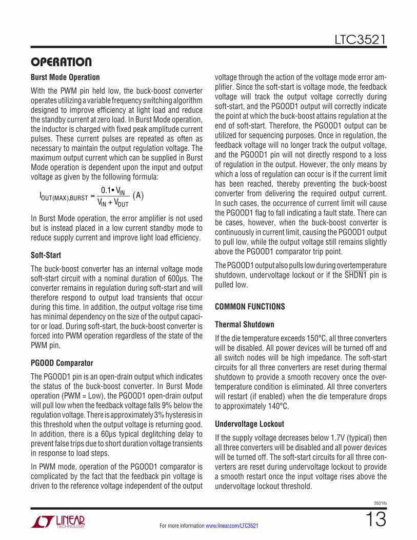
revision hisToryREV DATE DESCRIPTION PAGE NUMBER
A 11/10 Addition of PGND1A reflected throughout data sheet
Addition of VIN to Typical Applications 1, 19, 22
Revised Note 2 3
Changes to Block Diagram 9
Change to Operation Soft-Start section 11, 13
B 08/13 Corrected pin numbers on Block Diagram UF package 9
LTC3521
223521fb
For more information www.linear.com/LTC3521 LINEAR TECHNOLOGY CORPORATION 2010
LT 0813 REV B • PRINTED IN USALinear Technology Corporation1630 McCarthy Blvd., Milpitas, CA 95035-7417(408) 432-1900 ● FAX: (408) 434-0507 ● www.linear.com/LTC3521
relaTeD parTsPART NUMBER DESCRIPTION COMMENTS
LTC3100 700mA ISW, 1.5MHz, Synchronous Step-Up, 250mA Synchronous Step-Down DC/DC Converter and 100mA LDO
94% Efficiency, VIN: 0.7V to 5V, VOUT(MAX) = 5.25V, IQ = 15µA, ISD < 1µA, 3mm × 3mm QFN-16 Package
LTC3101 Wide VIN, Multioutput DC/DC Converter and PowerPath™ Controller, 800mA Buck-Boost, Dual 350mA Buck Converters, 50mA Always-On LDO
95% Efficiency, VIN: 1.8V to 5.5V, IQ = 38µA, Standby IQ = 15µA, 4mm × 4mm QFN-24 Package
LTC3409 600mA IOUT, 1.7MHz/2.6MHz, Synchronous Step-Down DC/DC Converter
96% Efficiency, VIN: 1.6V to 5.5V, VOUT(MIN) = 0.6V, IQ = 65µA, ISD < 1µA, DFN Package
LTC3441/LTC3442/LTC3443
1.2A IOUT, 2MHz, Synchronous Buck-Boost DC/DC Converter
95% Efficiency, VIN: 2.4V to 5.5V, VOUT(MIN): 2.4V to 5.25V, IQ = 50µA, ISD < 1µA, DFN Package
LTC3520 1A 2MHz, Synchronous Buck-Boost and 600mA Buck Converter
95% Efficiency, VIN: 2.2V to 5.5V, VOUT(MAX) = 5.25V, IQ = 55µA, ISD < 1µA, 4mm × 4mm QFN-24 Package
LTC3522 400mA 2MHz, Synchronous Buck-Boost and 200mA Buck Converter
95% Efficiency, VIN: 2.4V to 5.5V, VOUT(MAX) = 5.25V, IQ = 25µA, ISD < 1µA, 3mm × 3mm QFN-16 Package
LTC3531/LTC3531-3/ LTC3531-3.3
200mA IOUT, 1.5MHz, Synchronous Buck-Boost DC/DC Converter
95% Efficiency, VIN: 1.8V to 5.5V, VOUT(MIN): 2V to 5V, IQ = 16µA, ISD < 1µA, ThinSOT and DFN Packages
LTC3532 500mA IOUT, 2MHz, Synchronous Buck-Boost DC/DC Converter
95% Efficiency, VIN: 2.4V to 5.5V, VOUT(MIN): 2.4V to 5.25V, IQ = 35µA, ISD < 1µA, MS10 and DFN Packages
LTC3547 Dual 300mA IOUT, 2.25MHz, Synchronous Step-Down DC/DC Converter
95% Efficiency, VIN: 2.5V to 5.5V, VOUT(MIN) = 0.6V, IQ = 40µA, ISD < 1µA, DFN-8 Package
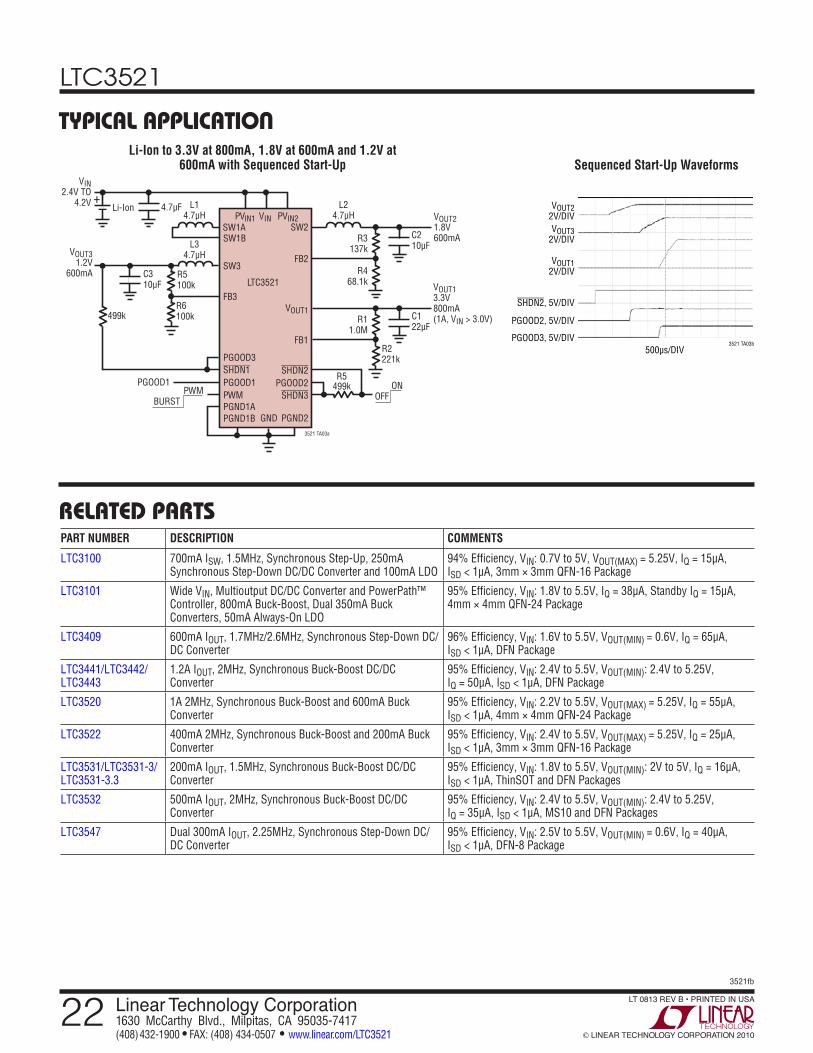
Typical applicaTionLi-Ion to 3.3V at 800mA, 1.8V at 600mA and 1.2V at
600mA with Sequenced Start-Up Sequenced Start-Up Waveforms
PVIN1 PVIN2SW2
VOUT1
FB2
FB1
SW3
LTC3521
SHDN1
R5100k
R3137k
R468.1k
C310µF
C210µF
4.7µFLi-Ion L14.7µH
L34.7µH
L24.7µH VOUT2
1.8V600mA
R11.0M
R2221k
C122µF
VOUT13.3V800mA(1A, VIN > 3.0V)
VIN2.4V TO
4.2V
R6100k499k
R5499k
3521 TA03a
PGOOD1
PGOOD3
PWM
SW1ASW1B
FB3
PGOOD2SHDN2
SHDN3PGOOD1
PGND2GND
PWMBURST
ONOFF
VOUT31.2V
600mA
+
PGND1APGND1B
VIN
500µs/DIV
VOUT22V/DIVVOUT3
2V/DIV
VOUT12V/DIV
SHDN2, 5V/DIV
PGOOD2, 5V/DIV
PGOOD3, 5V/DIV3521 TA03b
Related Documents